CN115516585A - Coil inductor and manufacturing method thereof - Google Patents
Coil inductor and manufacturing method thereofDownload PDFInfo
- Publication number
- CN115516585A CN115516585ACN202280001760.7ACN202280001760ACN115516585ACN 115516585 ACN115516585 ACN 115516585ACN 202280001760 ACN202280001760 ACN 202280001760ACN 115516585 ACN115516585 ACN 115516585A
- Authority
- CN
- China
- Prior art keywords
- conductive
- coil
- insulating film
- film
- disposed
- Prior art date
- Legal status (The legal status is an assumption and is not a legal conclusion. Google has not performed a legal analysis and makes no representation as to the accuracy of the status listed.)
- Pending
Links
Images


Classifications
- H—ELECTRICITY
- H01—ELECTRIC ELEMENTS
- H01F—MAGNETS; INDUCTANCES; TRANSFORMERS; SELECTION OF MATERIALS FOR THEIR MAGNETIC PROPERTIES
- H01F17/00—Fixed inductances of the signal type
- H01F17/0006—Printed inductances
- H01F17/0013—Printed inductances with stacked layers
- H—ELECTRICITY
- H01—ELECTRIC ELEMENTS
- H01F—MAGNETS; INDUCTANCES; TRANSFORMERS; SELECTION OF MATERIALS FOR THEIR MAGNETIC PROPERTIES
- H01F27/00—Details of transformers or inductances, in general
- H01F27/28—Coils; Windings; Conductive connections
- H01F27/32—Insulating of coils, windings, or parts thereof
- H—ELECTRICITY
- H01—ELECTRIC ELEMENTS
- H01F—MAGNETS; INDUCTANCES; TRANSFORMERS; SELECTION OF MATERIALS FOR THEIR MAGNETIC PROPERTIES
- H01F27/00—Details of transformers or inductances, in general
- H01F27/28—Coils; Windings; Conductive connections
- H01F27/30—Fastening or clamping coils, windings, or parts thereof together; Fastening or mounting coils or windings on core, casing, or other support
- H01F27/306—Fastening or mounting coils or windings on core, casing or other support
- H—ELECTRICITY
- H01—ELECTRIC ELEMENTS
- H01F—MAGNETS; INDUCTANCES; TRANSFORMERS; SELECTION OF MATERIALS FOR THEIR MAGNETIC PROPERTIES
- H01F27/00—Details of transformers or inductances, in general
- H01F27/28—Coils; Windings; Conductive connections
- H01F27/2823—Wires
- H01F27/2828—Construction of conductive connections, of leads
- H—ELECTRICITY
- H01—ELECTRIC ELEMENTS
- H01F—MAGNETS; INDUCTANCES; TRANSFORMERS; SELECTION OF MATERIALS FOR THEIR MAGNETIC PROPERTIES
- H01F27/00—Details of transformers or inductances, in general
- H01F27/28—Coils; Windings; Conductive connections
- H01F27/32—Insulating of coils, windings, or parts thereof
- H01F27/323—Insulation between winding turns, between winding layers
- H—ELECTRICITY
- H01—ELECTRIC ELEMENTS
- H01F—MAGNETS; INDUCTANCES; TRANSFORMERS; SELECTION OF MATERIALS FOR THEIR MAGNETIC PROPERTIES
- H01F17/00—Fixed inductances of the signal type
- H01F17/04—Fixed inductances of the signal type with magnetic core
- H01F2017/048—Fixed inductances of the signal type with magnetic core with encapsulating core, e.g. made of resin and magnetic powder
Landscapes
- Engineering & Computer Science (AREA)
- Power Engineering (AREA)
- Microelectronics & Electronic Packaging (AREA)
- Coils Or Transformers For Communication (AREA)
Abstract
Translated fromChinese
Description
Translated fromChinese技术领域technical field
本公开涉及线圈电感器和用于制造线圈电感器的方法。The present disclosure relates to coil inductors and methods for manufacturing coil inductors.
背景技术Background technique
线圈电感器通常用于电气应用,可分为用于信号处理的射频(RF)电感器和用于电源线的功率电感器。在RF电感器的应用中,线圈电感器可用于扼流、阻塞、衰减或过滤/平滑电路中的高频噪声。在功率电感器的应用中,功率电感器形成DC-DC转换器或其它设备中的电压转换电路的一部分。例如,在升压、降压或升压/降压电路中使用功率电感器将特定电压转换为所需电压。Coil inductors are commonly used in electrical applications and can be divided into radio frequency (RF) inductors for signal processing and power inductors for power lines. In RF inductor applications, coil inductors can be used to choke, block, attenuate, or filter/smooth high frequency noise in circuits. In power inductor applications, the power inductor forms part of a voltage conversion circuit in a DC-DC converter or other device. For example, a power inductor is used in a step-up, step-down or step-up/buck circuit to convert a specific voltage to a desired voltage.
发明内容Contents of the invention
在一个方面,公开了一种线圈电感器。线圈电感器包括第一导电线圈、第二导电线圈、第三导电线圈、第一绝缘膜和第二绝缘膜。第一绝缘膜设置在第一导电线圈上,且第一绝缘膜包括至少一个第一通孔。第二导电线圈设置在第一绝缘膜上。第二绝缘膜设置在第二导电线圈上,且第二绝缘膜包括至少一个不与第一通孔对齐的第二通孔。第三导电线圈设置在第二绝缘膜上。第一导电线圈通过设置在第一通孔中的第一触点与第二导电线圈电接触,第二导电线圈通过设置在第二通孔中的第二触点与第三导电线圈电接触。第一导电线圈、第二导电线圈和第三导电线圈的第一厚度在20微米和100微米之间。第一绝缘膜和第二绝缘膜的第二厚度在5微米和50微米之间。In one aspect, a coil inductor is disclosed. The coil inductor includes a first conductive coil, a second conductive coil, a third conductive coil, a first insulating film, and a second insulating film. The first insulating film is disposed on the first conductive coil, and the first insulating film includes at least one first through hole. The second conductive coil is disposed on the first insulating film. A second insulating film is disposed on the second conductive coil, and the second insulating film includes at least one second through hole that is not aligned with the first through hole. The third conductive coil is disposed on the second insulating film. The first conductive coil is in electrical contact with the second conductive coil through a first contact disposed in the first through hole, and the second conductive coil is in electrical contact with the third conductive coil through a second contact disposed in the second through hole. The first thickness of the first conductive coil, the second conductive coil and the third conductive coil is between 20 microns and 100 microns. The second thickness of the first insulating film and the second insulating film is between 5 microns and 50 microns.
在另一方面,公开了一种线圈电感器。线圈电感器包括第一导电线圈、设置在第一导电线圈上的第一绝缘膜、以及设置在第一绝缘膜上的第二导电线圈。第一导电线圈包括沿第一方向堆叠的多个第一导电膜。第一绝缘膜沿着垂直于第一方向的第二方向延伸,且包括至少一个通孔。第二导电线圈包括沿第一方向堆叠的多个第二导电膜。第一导电线圈通过设置在通孔中的第一触点与第二导电线圈电接触。In another aspect, a coil inductor is disclosed. The coil inductor includes a first conductive coil, a first insulating film disposed on the first conductive coil, and a second conductive coil disposed on the first insulating film. The first conductive coil includes a plurality of first conductive films stacked in a first direction. The first insulating film extends along a second direction perpendicular to the first direction, and includes at least one through hole. The second conductive coil includes a plurality of second conductive films stacked in the first direction. The first conductive coil is in electrical contact with the second conductive coil through a first contact disposed in the through hole.
在又一方面,公开了一种线圈电感器。线圈电感器包括设置在第一绝缘膜上方的第一导电膜、设置在第一绝缘膜下方的第二导电膜、设置在第二绝缘膜上方的第三导电膜和设置在第二绝缘膜下方的第四导电膜。第一导电膜和第二导电膜通过形成在第一绝缘膜中的第一触点电接触。第三导电膜和第四导电膜通过形成在第二绝缘膜中的第二触点电接触。第二导电膜附着到第三导电膜。In yet another aspect, a coil inductor is disclosed. The coil inductor includes a first conductive film provided above the first insulating film, a second conductive film provided below the first insulating film, a third conductive film provided above the second insulating film, and a second conductive film provided below the second insulating film. The fourth conductive film. The first conductive film and the second conductive film are in electrical contact through a first contact formed in the first insulating film. The third conductive film and the fourth conductive film are in electrical contact through a second contact formed in the second insulating film. The second conductive film is attached to the third conductive film.
在又一方面,公开了一种功率转换系统。所述功率转换系统包括被配置成将源电压转换成所需电压的线圈电感器,以及耦合到线圈电感器的控制器。线圈电感器包括第一导电线圈、第二导电线圈、第三导电线圈、第一绝缘膜和第二绝缘膜。第一绝缘膜设置在第一导电线圈上,且第一绝缘膜包括至少一个第一通孔。第二导电线圈设置在第一绝缘膜上。第二绝缘膜设置在第二导电线圈上,且第二绝缘膜包括至少一个不与第一通孔对齐的第二通孔。第三导电线圈设置在第二绝缘膜上。第一导电线圈通过设置在第一通孔中的第一触点与第二导电线圈电接触,第二导电线圈通过设置在第二通孔中的第二触点与第三导电线圈电接触。第一导电线圈、第二导电线圈和第三导电线圈的第一厚度在20微米和100微米之间。第一绝缘膜和第二绝缘膜的第二厚度在5微米和50微米之间。控制器耦合到线圈电感器,并被配置成控制线圈电感器的操作。In yet another aspect, a power conversion system is disclosed. The power conversion system includes a coil inductor configured to convert a source voltage to a desired voltage, and a controller coupled to the coil inductor. The coil inductor includes a first conductive coil, a second conductive coil, a third conductive coil, a first insulating film, and a second insulating film. The first insulating film is disposed on the first conductive coil, and the first insulating film includes at least one first through hole. The second conductive coil is disposed on the first insulating film. A second insulating film is disposed on the second conductive coil, and the second insulating film includes at least one second through hole that is not aligned with the first through hole. The third conductive coil is disposed on the second insulating film. The first conductive coil is in electrical contact with the second conductive coil through a first contact disposed in the first through hole, and the second conductive coil is in electrical contact with the third conductive coil through a second contact disposed in the second through hole. The first thickness of the first conductive coil, the second conductive coil and the third conductive coil is between 20 microns and 100 microns. The second thickness of the first insulating film and the second insulating film is between 5 microns and 50 microns. A controller is coupled to the coil inductor and configured to control operation of the coil inductor.
在又一方面,公开了一种功率转换系统。所述功率转换系统包括被配置成将源电压转换成所需电压的线圈电感器,以及耦合到线圈电感器的控制器。线圈电感器包括第一导电线圈、设置在第一导电线圈上的第一绝缘膜、以及设置在第一绝缘膜上的第二导电线圈。第一导电线圈包括沿第一方向堆叠的多个第一导电膜。第一绝缘膜沿着垂直于第一方向的第二方向延伸,且包括至少一个通孔。第二导电线圈包括沿第一方向堆叠的多个第二导电膜。第一导电线圈通过设置在通孔中的第一触点与第二导电线圈电接触。In yet another aspect, a power conversion system is disclosed. The power conversion system includes a coil inductor configured to convert a source voltage to a desired voltage, and a controller coupled to the coil inductor. The coil inductor includes a first conductive coil, a first insulating film disposed on the first conductive coil, and a second conductive coil disposed on the first insulating film. The first conductive coil includes a plurality of first conductive films stacked in a first direction. The first insulating film extends along a second direction perpendicular to the first direction, and includes at least one through hole. The second conductive coil includes a plurality of second conductive films stacked in the first direction. The first conductive coil is in electrical contact with the second conductive coil through a first contact disposed in the through hole.
在又一方面,公开了一种功率转换系统。所述功率转换系统包括被配置成将源电压转换成所需电压的线圈电感器,以及耦合到线圈电感器的控制器。线圈电感器包括设置在第一绝缘膜上方的第一导电膜、设置在第一绝缘膜下方的第二导电膜、设置在第二绝缘膜上方的第三导电膜和设置在第二绝缘膜下方的第四导电膜。第一导电膜和第二导电膜通过形成在第一绝缘膜中的第一触点电接触。第三导电膜和第四导电膜通过形成在第二绝缘膜中的第二触点电接触。第二导电膜附着到第三导电膜。In yet another aspect, a power conversion system is disclosed. The power conversion system includes a coil inductor configured to convert a source voltage to a desired voltage, and a controller coupled to the coil inductor. The coil inductor includes a first conductive film provided above the first insulating film, a second conductive film provided below the first insulating film, a third conductive film provided above the second insulating film, and a second conductive film provided below the second insulating film. The fourth conductive film. The first conductive film and the second conductive film are in electrical contact through a first contact formed in the first insulating film. The third conductive film and the fourth conductive film are in electrical contact through a second contact formed in the second insulating film. The second conductive film is attached to the third conductive film.
在又一方面,公开了一种用于形成线圈电感器的制造方法。堆叠多个第一导电膜以形成第一导电线圈。堆叠多个第二导电膜以形成第二导电线圈。第一导电线圈、第一绝缘膜和第二导电线圈堆叠在一起。第一导电线圈通过形成在第一绝缘膜中的第一触点与第二导电线圈电接触。In yet another aspect, a fabrication method for forming a coil inductor is disclosed. A plurality of first conductive films are stacked to form a first conductive coil. A plurality of second conductive films are stacked to form a second conductive coil. The first conductive coil, the first insulating film and the second conductive coil are stacked together. The first conductive coil is in electrical contact with the second conductive coil through a first contact formed in the first insulating film.
附图说明Description of drawings
并入本文并形成说明书的一部分的附图示出了本公开的各个方面,并与具体实施方式一起进一步用于解释本公开并使相关领域的技术人员能够制作和使用本公开。The accompanying drawings, which are incorporated in and form a part of this specification, illustrate various aspects of the disclosure and, together with the detailed description, further serve to explain the disclosure and enable those skilled in the relevant arts to make and use the disclosure.
图1示出了根据本公开的一些方面的示例性线圈电感器的横截面。FIG. 1 illustrates a cross-section of an exemplary coil inductor according to some aspects of the present disclosure.
图2-6示出了根据本公开的一些方面的示例性线圈电感器的平面图。2-6 illustrate plan views of example coil inductors according to some aspects of the present disclosure.
图7示出了根据本公开的一些方面的示例性线圈电感器的横截面。7 illustrates a cross-section of an example coil inductor according to some aspects of the present disclosure.
图8-13示出了根据本公开的一些方面的示例性线圈电感器的平面图。8-13 illustrate plan views of exemplary coil inductors according to some aspects of the present disclosure.
图14示出了根据本公开的一些方面的构造示例性线圈电感器的导电结构的横截面。14 illustrates a cross-section of a conductive structure constructing an exemplary coil inductor in accordance with aspects of the present disclosure.
图15示出了根据本公开的一些方面的示例性线圈电感器的横截面。15 illustrates a cross-section of an example coil inductor according to some aspects of the present disclosure.
图16A-16B示出了根据本公开的一些方面的示例性线圈电感器的横截面。16A-16B illustrate cross-sections of exemplary coil inductors according to some aspects of the present disclosure.
图17示出了根据本公开的一些方面的用于形成线圈电感器的示例性方法的流程图。17 shows a flowchart of an example method for forming a coil inductor in accordance with some aspects of the present disclosure.
图18示出了根据本公开的一些方面的具有线圈电感器的示例性功率转换系统的框图。18 illustrates a block diagram of an example power conversion system with coil inductors, according to some aspects of the present disclosure.
将参考附图描述本公开。The present disclosure will be described with reference to the accompanying drawings.
具体实施方式detailed description
尽管论述了具体的配置和布置,但应理解,这仅仅是为了说明的目的。这样,在不脱离本公开的范围的情况下,可以使用其它配置和布置。此外,本公开还可以用于各种其它应用。在本公开中描述的功能和结构特征可以以未在附图中具体描述的方式相互组合、调整和修改,使得这些组合、调整和修改在本公开的范围内。While specific configurations and arrangements are discussed, it should be understood that this is done for illustration purposes only. As such, other configurations and arrangements may be used without departing from the scope of the present disclosure. In addition, the present disclosure can also be used in various other applications. The functions and structural features described in the present disclosure may be combined, adjusted, and modified with each other in ways not specifically described in the drawings, so that these combinations, adjusted, and modified are within the scope of the present disclosure.
一般而言,术语可以至少部分地从上下文中的使用来理解。例如,这里使用的术语“一个或多个”,至少部分取决于上下文,可以用来描述单数意义上的任何特征、结构或特性,或者可以用来描述复数意义上的特征、结构或特性的组合。类似地,诸如“一个(a/an)”或“所述(the)”的术语同样可以被理解为传达单数用法或传达复数用法,这至少部分取决于上下文。此外,术语“基于”可以被理解为不一定意在传达一组排他的因素,而是可以允许不一定明确描述的附加因素的存在,同样,至少部分取决于上下文。In general, a term can be understood at least in part from its usage in context. For example, the term "one or more", as used herein, may be used to describe any feature, structure, or characteristic in the singular, or may be used to describe a combination of features, structures, or characteristics in the plural, depending at least in part on the context . Similarly, terms such as "a/an" or "the" may equally be read to convey singular usage or to convey plural usage, depending at least in part on context. Furthermore, the term "based on" may be understood as not necessarily intended to convey an exclusive set of factors, but rather may allow for the presence of additional factors not necessarily explicitly described, again depending, at least in part, on context.
应容易理解的是,本公开中的“上(on)”和“上方(above/over)”的含义应以最广泛的方式解释,使得“上”不仅意味着“直接在”某物上,而且还包括“在”其间具有中间特征或层的某物上的含义,且“上方”不仅意味着“在”某物上方的含义,而且还可以包括它在其间没有中间特征或层的某物“上方”的含义(即,直接在某物上)。It should be readily understood that the meanings of "on" and "above/over" in this disclosure are to be interpreted in the broadest manner such that "on" does not only mean "directly on" something, but also includes the meaning of "on" something with intermediate features or layers in between, and "above" means not only "on" something, but it can also include something that has no intermediate features or layers in between Meaning of "above" (ie, directly on something).
此外,为了便于描述,这里可以使用空间上相对的术语,例如“下面(beneath)”、“下方(below)”、“下部(lower)”、“上方(above)”、“上部(upper)”等,来描述一个元件或特征与图中所示的另一个元件或特征的关系。除了图中所示的方位之外,空间相对术语旨在涵盖使用或操作中设备的不同方位。所述装置可以以其它方式定向(旋转90度或其它方向),且这里使用的空间相对描述符同样可以相应地解释。In addition, for the convenience of description, spatially relative terms may be used here, such as "beneath", "below", "lower", "above", "upper" etc., to describe the relationship of one element or feature to another element or feature shown in the figures. Spatially relative terms are intended to encompass different orientations of the device in use or operation in addition to the orientation depicted in the figures. The device may be otherwise oriented (rotated 90 degrees or at other orientations) and the spatially relative descriptors used herein interpreted accordingly.
如本文所用,术语“层”是指包括具有厚度的区域的材料部分。一层可以在整个下层或上层结构上延伸,或者可以具有小于下层或上层结构的范围。此外,层可以是均匀或非均匀连续结构的区域,其厚度小于连续结构的厚度。例如,层可以位于连续结构的顶面和底面之间或之上的任何一对水平面之间。层可以水平、垂直和/或沿着锥形表面延伸。基底可以是一层,其中可以包括一层或多层,和/或其上、其上方和/或其下方可以具有一层或多层。一个层可以包括多个层。例如,互连层可以包括一个或多个导体和接触层(其中形成互连线和/或通孔接触)以及一个或多个介电层。As used herein, the term "layer" refers to a portion of material that includes regions having a thickness. A layer may extend across the entire underlying or superstructure, or may have a smaller extent than the underlying or superstructure. Furthermore, a layer may be a region of uniform or non-uniform continuous structure, the thickness of which is less than that of the continuous structure. For example, a layer may be located between any pair of levels between or above the top and bottom surfaces of the continuous structure. Layers may extend horizontally, vertically and/or along the tapered surface. A substrate can be one layer, can include one or more layers therein, and/or can have one or more layers thereon, above, and/or below. A layer can consist of multiple layers. For example, interconnect layers may include one or more conductor and contact layers (in which interconnect lines and/or via contacts are formed) and one or more dielectric layers.
如本文所用,术语“线圈”指代由缠绕成连续系列环的物件组成的结构。线圈的形状可以是圆形、正方形、矩形、椭圆形、三角形或任何多边形。线圈可以以螺旋路线缠绕或移动。在一些实施方式中,线圈是螺旋形电极的通称。在一些实施方式中,电感器也可以被称为线圈。电感器是一种无源双端电气元件,当电流流过时,其在磁场中储存能量。电感器通常由缠绕成线圈的绝缘线组成。As used herein, the term "coil" refers to a structure consisting of an object wound into a continuous series of loops. The shape of the coil can be circular, square, rectangular, oval, triangular or any polygon. Coils can be wound or moved in a helical course. In some embodiments, a coil is a general term for a helical electrode. In some embodiments, an inductor may also be referred to as a coil. An inductor is a passive two-terminal electrical component that stores energy in a magnetic field when current flows through it. Inductors usually consist of insulated wire wound into a coil.
电路的电感取决于电流路径的几何形状以及附近材料的磁导率。电感器可以由导线或其它导体组成,其形状可以增加通过电路的磁通量,通常为线圈或螺旋形状,具有两个端子。将电线绕成线圈增加了磁力线连接电路的次数,从而增加了磁场,进而增加了电感。匝数越多,电感越高。电感还取决于线圈的形状、线匝的间隔以及许多其它因素。通过在线圈内添加由铁等铁磁材料制成的“磁芯”,线圈的磁化场将在材料中感应磁化,增加磁通量。铁磁芯的高磁导率可以使线圈的电感比没有它时增加几千倍。The inductance of a circuit depends on the geometry of the current path and the permeability of nearby materials. An inductor can consist of wire or other conductors shaped to increase the magnetic flux through a circuit, usually in the shape of a coil or helix, with two terminals. Winding the wire into a coil increases the number of times the magnetic field lines connect the circuit, which increases the magnetic field, which in turn increases the inductance. The more turns, the higher the inductance. Inductance also depends on the shape of the coil, the spacing of the turns, and many other factors. By adding a "core" made of ferromagnetic material such as iron inside the coil, the coil's magnetizing field will induce magnetization in the material, increasing the magnetic flux. The high magnetic permeability of the ferromagnetic core can increase the inductance of the coil thousands of times over what it would be without it.
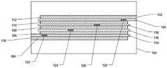
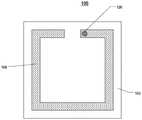
图1示出了根据本公开的一些方面的示例性线圈电感器100的横截面。图2-6示出了根据本公开的一些方面的线圈电感器100的不同层的平面图。为了更好地描述本公开,将一起论述图1和图2-6中的线圈电感器100的横截面和平面图。FIG. 1 illustrates a cross-section of an
如图1所示,线圈电感器100可以包括磁体102、多个导电线圈和设置在两个相邻导电线圈之间的多个绝缘膜。例如,第一导电线圈104和第二导电线圈106可以由第一绝缘膜114分开,第二导电线圈106和第三导电线圈108可以由第二绝缘膜116分开,第三导电线圈108和第四导电线圈110可以由第三绝缘膜118分开,第四导电线圈110和第五导电线圈112可以由第四绝缘膜120分开。应理解,图1中所示的五层导电线圈仅用于说明目的,根据不同的要求,电感器结构可以具有多于五层或少于五层的导电线圈。As shown in FIG. 1 , a
在一些实施方式中,磁体102可以由磁性合金粉末和粘合剂的混合物形成。在一些实施方式中,混合物可以是粉末或糊状物。在一些实施方式中,混合物可以包括铁氧体材料,所述铁氧体材料包含Fe、Ni、Zn和/或Cu的相应成分作为主要成分。在一些实施方式中,混合物可以包括含有镍-铜-锌基铁氧体材料、镍-铜-锌-镁基铁氧体材料和/或镍-铜基铁氧体材料的铁氧体材料。在一些实施方式中,混合物可以包括铁氧体烧结体。In some embodiments, the
在一些实施方式中,多个导电线圈和多个绝缘膜被嵌入混合物中,且混合物可以被烘焙或固化以固化形成磁体102。在一些实施方式中,在将多个导电线圈和多个绝缘膜嵌入混合物中之后,可以对混合物进行压缩处理以增强混合物的致密性,然后可以进行烘焙工艺以固化混合物。In some embodiments, a plurality of conductive coils and a plurality of insulating films are embedded in the mixture, and the mixture may be baked or cured to cure to form the
在一些实施方式中,第一导电线圈104、第二导电线圈106、第三导电线圈108、第四导电线圈110和第五导电线圈112可以由金属形成。在一些实施方式中,第一导电线圈104、第二导电线圈106、第三导电线圈108、第四导电线圈110和第五导电线圈112可以由铜膜或铜箔形成。在一些实施方式中,第一导电线圈104、第二导电线圈106、第三导电线圈108、第四导电线圈110和第五导电线圈112的厚度可以在20微米和100微米之间的范围内。In some embodiments, the first
在一些实施方式中,第一绝缘膜114、第二绝缘膜116、第三绝缘膜118和第四绝缘膜120可以由非导电材料形成。在一些实施方式中,第一绝缘膜114、第二绝缘膜116、第三绝缘膜118和第四绝缘膜120可以由聚酰亚胺膜形成。在一些实施方式中,第一绝缘膜114、第二绝缘膜116、第三绝缘膜118和第四绝缘膜120的厚度可以在5微米和50微米之间的范围内。In some embodiments, the first insulating
在一些实施方式中,第一绝缘膜114、第二绝缘膜116、第三绝缘膜118和第四绝缘膜120的厚度可以在15微米和30微米之间的范围内。In some embodiments, the thickness of the first insulating
如图1和图2-6所示,第一绝缘膜114、第二绝缘膜116、第三绝缘膜118和第四绝缘膜120中的每一个均可以包括至少一个通孔。在一些实施方式中,第一触点122可以形成在第一绝缘膜114的通孔中,第二触点124可以形成在第二绝缘膜116的通孔中,第三触点126可以形成在第三绝缘膜118的通孔中,第四触点128可以形成在第四绝缘膜120的通孔中。在一些实施方式中,第一触点122可以将第一导电线圈104与第二导电线圈106电耦合,第二触点124可以将第二导电线圈106与第三导电线圈108电耦合,第三触点126可以将第三导电线圈108与第四导电线圈110电耦合,且第四触点128可以将第四导电线圈110与第五导电线圈112电耦合。As shown in FIGS. 1 and 2-6 , each of the first insulating
在一些实施方式中,第一触点122、第二触点124、第三触点126和第四触点128可以由导电材料形成。在一些实施方式中,第一触点122、第二触点124、第三触点126和第四触点128可以由铜形成。在一些实施方式中,在线圈电感器100的侧视图中,第一触点122、第二触点124、第三触点126和第四触点128可以不对齐。换句话说,在线圈电感器100的平面图中,第一触点122、第二触点124、第三触点126和第四触点128可以彼此不重叠。In some implementations, the
线圈电感器100还可以包括第一端130和第二端132。在一些实施方式中,第一端130可以设置在导电线圈104上,第二端132可以设置在第五导电线圈112上。第一端130和第二端132可以电耦合到外部端子。在一些实施方式中,线圈电感器100中的电流路径可以从第一端130开始,如图2所示,且穿过第一导电线圈104和第一触点122进入第二导电线圈106。然后,电流路径通过第二导电线圈106和第二触点124,如图3所示,并进入第三导电线圈108。如图4所示,电流路径穿过第三导电线圈108和第三触点126,并进入第四导电线圈110。如图5所示,电流路径穿过第四导电线圈110和第四触点128,并进入第五导电线圈112。如图6所示,电流路径穿过第五导电线圈112并在第二端132输出。The
通过堆叠多层导电线圈和绝缘膜,并使用光刻操作和电镀工艺来形成相邻导电线圈之间的接触,线圈电感器100可以包括多于三个线圈层。此外,通过使用薄导电线圈和薄绝缘膜来形成线圈叠层,线圈电感器100的厚度可以进一步减小。The
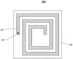
图7示出了根据本公开的一些方面的示例性线圈电感器200的横截面。图8-13示出了根据本公开的一些方面的线圈电感器200的平面图。为了更好地描述本公开,将一起论述图7和图8-13中的线圈电感器200的横截面和平面图。FIG. 7 illustrates a cross-section of an
如图7所示,线圈电感器200可以包括磁体202、多个导电线圈和设置在两个相邻导电线圈之间的多个绝缘膜。例如,第一导电线圈204和第二导电线圈206可以由第一绝缘膜216分开,第二导电线圈206和第三导电线圈208可以由第二绝缘膜218分开,第三导电线圈208和第四导电线圈210可以由第三绝缘膜220分开,第四导电线圈210和第五导电线圈212可以由第四绝缘膜222分开,且第五导电线圈212和第六导电线圈214可以由第五绝缘膜224分开。在一些实施方式中,线圈电感器200可以类似于线圈电感器100,且不同之处在于图8-13所示的触点位置、线圈层数和线圈的线圈设计。As shown in FIG. 7, the
如图8-13所示,线圈电感器200可以包括六层导电线圈,且第一导电线圈204、第二导电线圈206、第三导电线圈208、第四导电线圈210、第五导电线圈212和第六导电线圈214中的每一个可以包括多于一个线圈环。例如,第一导电线圈204、第二导电线圈206、第三导电线圈208、第四导电线圈210、第五导电线圈212和第六导电线圈214中的每一个可以包括2.5个线圈环。As shown in FIGS. 8-13, the
在一些实施方式中,第一触点226可以将第一导电线圈204与第二导电线圈206电耦合,第二触点228可以将第二导电线圈206与第三导电线圈208电耦合,第三触点230可以将第三导电线圈208与第四导电线圈210电耦合,第四触点232可以将第四导电线圈210与第五导电线圈212电耦合,且第五触点234可以将第五导电线圈212与第六导电线圈214电耦合。在一些实施方式中,在线圈电感器200的侧面,第一触点226、第三触点230和第五触点234可以彼此对齐。换句话说,在线圈电感器200的平面图中,第一触点226、第三触点230和第五触点234可以彼此重叠。在一些实施方式中,在线圈电感器200的侧面,第二触点228和第四触点232可以彼此对齐。换句话说,在线圈电感器200的平面图中,第二触点228和第四触点232可以彼此重叠。In some embodiments, the
图14示出了根据本公开的一些方面的构造示例性线圈电感器的导电结构502、504A和504B的横截面。如图14所示,导电结构502包括支撑件512和导电膜514。在一些实施方式中,支撑件512可以包括柔性膜,导电膜514可以包括铜膜。在一些实施方式中,支撑件512可以包括可剥离的材料,且可以在随后的过程中根据需要从导电膜514剥离和分离。在一些实施方式中,导电膜514可以具有5微米至120微米之间的厚度。在一些实施方式中,导电膜514可以具有5微米至100微米之间的厚度。在一些实施方式中,导电膜514可以具有5微米至50微米之间的厚度。在一些实施方式中,支撑件512可以具有50微米至200微米之间的厚度。FIG. 14 illustrates a cross-section of
在一些实施方式中,导电膜514可以形成线圈。在一些实施方式中,在导电膜514的平面图中,导电膜514可以是螺线管线圈、方形线圈、矩形线圈、椭圆形线圈、T型线圈或其它合适的形状。在一些实施方式中,导电膜514可以包括半圆形线圈。在一些实施方式中,导电膜514可以包括N圆线圈,且N大于1。In some implementations, the
如图14所示,导电结构504A可以包括绝缘膜516和设置在绝缘膜516两侧的两个导电膜518。在一些实施方式中,绝缘膜516可以包括绝缘材料,例如聚酰亚胺(PI)、聚对苯二甲酸乙二醇酯(PET)或其它合适的材料。在一些实施方式中,绝缘膜516可以具有5微米至100微米之间的厚度。在一些实施方式中,绝缘膜516可以具有5微米至50微米之间的厚度。在一些实施方式中,绝缘膜516可以具有5微米至20微米之间的厚度。每个导电膜518可以包括铜膜。在一些实施方式中,每个导电膜518可以具有5微米至120微米之间的厚度。在一些实施方式中,每个导电膜518可以具有5微米至100微米之间的厚度。在一些实施方式中,每个导电膜518可以具有5微米至50微米之间的厚度。As shown in FIG. 14 , the
如图14所示,绝缘膜516可以包括通孔,且接触520可以形成在通孔中。设置在绝缘膜516两侧的导电膜518可以通过触点520彼此电接触。在一些实施方式中,触点520可以包括与导电膜518相同的材料。在一些实施方式中,触点520可以包括铜。在一些实施方式中,触点520可以是在触点520的中心具有开口的中空结构,如图14中的导电结构504A所示。在一些实施方式中,设置在绝缘膜516两侧的导电膜518可以通过触点522彼此电接触。在一些实施方式中,触点522可以包括与导电膜518相同的材料。在一些实施方式中,触点522可以包括铜。在一些实施方式中,触点522可以是中心没有开口的实心结构,如图14中的导电结构504B所示。As shown in FIG. 14, the insulating
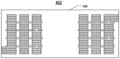
图15示出了根据本公开的一些方面的示例性线圈电感器600的横截面。线圈电感器600可以由导电结构502、导电结构504A和/或导电结构504B的任意组合形成。在一些实施方式中,通过组合导电结构502、导电结构504A和/或导电结构504B的不同数量和结构,线圈电感器600可以具有不同的变型,例如线圈电感器602、线圈电感器604或线圈电感器606,如图15所示。FIG. 15 illustrates a cross-section of an
线圈电感器602可以包括堆叠在一起的多个导电结构504B和多个导电结构502。具体地,在一些实施方式中,至少一个导电结构502可以设置在导电结构504B上,然后可以从导电结构502移除支撑件512,且导电膜514保留在导电结构504B上。导电膜514可以进一步与其它导电结构504B或其它导电膜514堆叠,以形成线圈电感器602,如图15所示。在一些实施方式中,导电膜514和导电结构504B可以通过粘合层结合或附着。在一些实施方式中,导电膜514和导电结构504B可以通过导电粘合层结合或附着。在一些实施方式中,导电膜514和导电结构504B可以通过铜结合操作来组合或附着。The
线圈电感器604可以包括多个导电结构504B。具体地,在一些实施方式中,至少两个导电结构504B堆叠在一起以形成线圈电感器604,如图15所示。在一些实施方式中,两个导电结构504B可以通过粘合层结合或附着。在一些实施方式中,两个导电结构504B可以通过导电粘合层结合或附着。在一些实施方式中,两个导电结构504B可以通过铜键合操作来组合或附着。
线圈电感器606可以包括至少一个导电结构504B和附着在导电结构504B两侧的多个导电膜514。如图15所示,导电结构504B包括在绝缘膜516两侧的两个导电膜518,且导电膜514可以附着在两个导电膜518上。在一些实施方式中,导电膜514和导电结构504B可以通过粘合层结合或附着。在一些实施方式中,导电膜514和导电结构504B可以通过导电粘合层结合或附着。在一些实施方式中,导电膜514和导电结构504B可以通过铜结合操作来组合或附着。The
图29A-29B示出了根据本公开的一些方面的线圈电感器602的横截面。在将导电膜514与导电结构504B堆叠之后,可以进一步执行切割操作以切割绝缘膜516的部分。在一些实施方式中,在线圈电感器602的平面图中,线圈电感器602的中心部分处的绝缘膜516可以被去除,如图16A所示。然后,如图16B所示,磁体608可以形成为覆盖导电线圈602。29A-29B illustrate a cross-section of a
在一些实施方式中,可以提供磁性合金混合物来完全覆盖线圈电感器602。在一些实施方式中,多个导电结构504B、多个导电膜514和绝缘膜516嵌入磁性合金混合物中。在一些实施方式中,磁性合金混合物可以包括磁性合金粉末和粘合剂。在一些实施方式中,磁性合金混合物可以是粉末或糊状物。在一些实施方式中,磁性合金混合物可以包括含有铁、镍、锌和/或铜的相应成分作为主要成分的铁氧体材料。在一些实施方式中,磁性合金混合物可以包括含有Ni-Cu-Zn基铁氧体材料、Ni-Cu-Zn-Mg基铁氧体材料和/或Ni-Cu基铁氧体材料的铁氧体材料。在一些实施方式中,磁性合金混合物可以包括铁氧体烧结体。In some implementations, a magnetic alloy mixture may be provided to completely cover the
然后,在一些实施方式中,可以通过软介质对磁性合金混合物执行压缩操作,以将磁性合金混合物压缩成磁体608。在一些实施方式中,软介质可以包围磁性合金混合物,以将磁性合金混合物压缩到磁体608。在一些实施方式中,软介质可以是液体介质。在一些实施方式中,液体介质可以包括水。Then, in some embodiments, a compression operation may be performed on the magnetic alloy mixture through a soft medium to compress the magnetic alloy mixture into
在一些实施方式中,可以进一步在磁体608的表面上执行平坦化操作。在使用软介质的压缩操作之后,磁体608的表面可能不平坦,且平坦化操作可以改善磁体608的表面的粗糙度。在一些实施方式中,平坦化操作可以包括研磨工艺。在一些实施方式中,磁体608可以被烘焙或固化以进一步固化磁体608。In some implementations, a planarization operation may further be performed on the surface of the
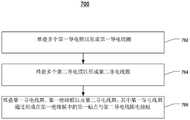
图17示出了根据本公开的一些方面的用于形成线圈电感器606的示例性方法700的流程图。在图17的操作702中,堆叠多个导电膜514以形成第一导电线圈。在图17的操作704中,堆叠多个导电膜514以形成第二导电线圈。在图17的操作706中,第一导电线圈和第二导电线圈被附着到导电结构504B的两侧。第一导电线圈通过形成在导电结构504B的绝缘膜516中的触点522与第二导电线圈电接触。FIG. 17 shows a flowchart of an
应理解,方法700中所示的操作不是穷举的,且在任何所示操作之前、之后或之间也可以执行其它操作。此外,一些操作可以同时执行,或者以不同于图17所示的顺序执行。例如,第一导电线圈和第二导电线圈可以同时形成,且同时附着到导电结构504B上。对于另一个例子,多个导电膜514可以一层一层地附着到导电结构504B。换句话说,操作702或操作704可以执行几次以形成具有所需厚度的导电线圈。It should be understood that the operations shown in
在一些实施方式中,可以堆叠更多的导电膜514以形成第三导电线圈,且第一导电线圈、导电结构504B、第二导电线圈、另一导电结构504B和第三导电线圈可以进一步堆叠在一起以形成导电线圈的附加层。In some embodiments, more
在一些实施方式中,在堆叠第一导电线圈、导电结构504B和第二导电线圈之后,可以执行切割操作以去除绝缘膜516的部分。然后,磁体可以形成为覆盖第一导电线圈、导电结构504B和第二导电线圈。In some implementations, after stacking the first conductive coil, the
通过灵活地组合导电结构502、导电结构504A和导电结构504B,可以通过堆叠导电结构502、导电结构504A和/或导电结构504B来形成具有任何所需厚度的导电线圈。由绝缘膜分开的导电线圈可以通过形成在绝缘膜中的触点彼此电接触。因此,线圈电感器可以以灵活的方式制造,以满足各种设计要求。By flexibly combining the
图18示出了根据本公开的一些方面的具有线圈电感器的示例性功率转换系统800的框图。在一些实施方式中,功率转换系统800是DC-DC转换器。在一些实施方式中,功率转换系统800可以应用于各种电源电路。例如,处理器、存储器、LED和其它设备需要许多不同的DC电压来运行,且功率转换系统800可以调节这些电压差。因此,在大多数电子设备中均需要功率转换系统800,且通常在一个设备中使用大量的功率转换系统。FIG. 18 shows a block diagram of an example
功率转换系统800可以包括控制器802、线圈电感器804和电容器806。线圈电感器804可以被配置成将源电压Vin转换成所需的电压Vout。控制器802可以耦合到线圈电感器804,且可以被配置成控制线圈电感器804的操作。线圈电感器804可以与电容器806一起工作,以起到将来自控制器802的矩形波输出整流成直流的作用。
根据本公开的一个方面,公开了一种线圈电感器。线圈电感器包括第一导电线圈、第二导电线圈、第三导电线圈、第一绝缘膜和第二绝缘膜。第一绝缘膜设置在第一导电线圈上,且第一绝缘膜包括至少一个第一通孔。第二导电线圈设置在第一绝缘膜上。第二绝缘膜设置在第二导电线圈上,且第二绝缘膜包括至少一个不与第一通孔对齐的第二通孔。第三导电线圈设置在第二绝缘膜上。第一导电线圈通过设置在第一通孔中的第一触点与第二导电线圈电接触,第二导电线圈通过设置在第二通孔中的第二触点与第三导电线圈电接触。第一导电线圈、第二导电线圈和第三导电线圈的第一厚度在20微米和100微米之间。第一绝缘膜和第二绝缘膜的第二厚度在5微米和50微米之间。According to one aspect of the present disclosure, a coil inductor is disclosed. The coil inductor includes a first conductive coil, a second conductive coil, a third conductive coil, a first insulating film, and a second insulating film. The first insulating film is disposed on the first conductive coil, and the first insulating film includes at least one first through hole. The second conductive coil is disposed on the first insulating film. A second insulating film is disposed on the second conductive coil, and the second insulating film includes at least one second through hole that is not aligned with the first through hole. The third conductive coil is disposed on the second insulating film. The first conductive coil is in electrical contact with the second conductive coil through a first contact disposed in the first through hole, and the second conductive coil is in electrical contact with the third conductive coil through a second contact disposed in the second through hole. The first thickness of the first conductive coil, the second conductive coil and the third conductive coil is between 20 microns and 100 microns. The second thickness of the first insulating film and the second insulating film is between 5 microns and 50 microns.
在一些实施方式中,线圈电感器还包括覆盖第一导电线圈、第二导电线圈、第三导电线圈、第一绝缘膜和第二绝缘膜的磁体。在一些实施方式中,第一绝缘膜和第二绝缘膜还包括聚酰亚胺膜。In some embodiments, the coil inductor further includes a magnet covering the first conductive coil, the second conductive coil, the third conductive coil, the first insulating film, and the second insulating film. In some embodiments, the first insulating film and the second insulating film further include a polyimide film.
在一些实施方式中,第一导电线圈、第二导电线圈和第三导电线圈还包括铜膜。在一些实施方式中,磁体由磁性合金粉末和粘合剂的混合物形成。In some embodiments, the first conductive coil, the second conductive coil, and the third conductive coil further include a copper film. In some embodiments, the magnet is formed from a mixture of magnetic alloy powder and a binder.
根据本公开的另一方面,公开了一种线圈电感器。线圈电感器包括第一导电线圈、设置在第一导电线圈上的第一绝缘膜、以及设置在第一绝缘膜上的第二导电线圈。第一导电线圈包括沿第一方向堆叠的多个第一导电膜。第一绝缘膜沿着垂直于第一方向的第二方向延伸,且包括至少一个通孔。第二导电线圈包括沿第一方向堆叠的多个第二导电膜。第一导电线圈通过设置在通孔中的第一触点与第二导电线圈电接触。According to another aspect of the present disclosure, a coil inductor is disclosed. The coil inductor includes a first conductive coil, a first insulating film disposed on the first conductive coil, and a second conductive coil disposed on the first insulating film. The first conductive coil includes a plurality of first conductive films stacked in a first direction. The first insulating film extends along a second direction perpendicular to the first direction, and includes at least one through hole. The second conductive coil includes a plurality of second conductive films stacked in the first direction. The first conductive coil is in electrical contact with the second conductive coil through a first contact disposed in the through hole.
在一些实施方式中,多个第一导电膜和多个第二导电膜分别通过粘合层结合。在一些实施方式中,多个第一导电膜和多个第二导电膜分别通过铜键合操作结合。In some embodiments, the plurality of first conductive films and the plurality of second conductive films are respectively bonded by an adhesive layer. In some embodiments, the plurality of first conductive films and the plurality of second conductive films are respectively bonded by a copper bonding operation.
在一些实施方式中,多个第一导电膜中的每一个具有5微米至120微米之间的厚度,多个第二导电膜中的每一个具有5微米至120微米之间的厚度。In some embodiments, each of the plurality of first conductive films has a thickness between 5 microns and 120 microns, and each of the plurality of second conductive films has a thickness of between 5 microns and 120 microns.
在一些实施方式中,第一触点包括中空结构。在一些实施方式中,第一触点包括固体结构。在一些实施方式中,第一绝缘膜的厚度在5微米和20微米之间。In some embodiments, the first contact includes a hollow structure. In some embodiments, the first contact includes a solid structure. In some embodiments, the thickness of the first insulating film is between 5 microns and 20 microns.
在一些实施方式中,线圈电感器还包括设置在第二导电线圈上的第二绝缘膜,以及设置在第二绝缘膜上的第三导电线圈。第三导电线圈包括沿第一方向堆叠的多个第三导电膜。第二导电线圈通过形成在第二绝缘膜中的第二触点与第三导电线圈电接触。In some embodiments, the coil inductor further includes a second insulating film disposed on the second conductive coil, and a third conductive coil disposed on the second insulating film. The third conductive coil includes a plurality of third conductive films stacked in the first direction. The second conductive coil is in electrical contact with the third conductive coil through a second contact formed in the second insulating film.
根据本公开的又一方面,公开了一种线圈电感器。线圈电感器包括设置在第一绝缘膜上方的第一导电膜、设置在第一绝缘膜下方的第二导电膜、设置在第二绝缘膜上方的第三导电膜和设置在第二绝缘膜下方的第四导电膜。第一导电膜和第二导电膜通过形成在第一绝缘膜中的第一触点电接触。第三导电膜和第四导电膜通过形成在第二绝缘膜中的第二触点电接触。第二导电膜附着到第三导电膜。According to yet another aspect of the present disclosure, a coil inductor is disclosed. The coil inductor includes a first conductive film provided above the first insulating film, a second conductive film provided below the first insulating film, a third conductive film provided above the second insulating film, and a second conductive film provided below the second insulating film. The fourth conductive film. The first conductive film and the second conductive film are in electrical contact through a first contact formed in the first insulating film. The third conductive film and the fourth conductive film are in electrical contact through a second contact formed in the second insulating film. The second conductive film is attached to the third conductive film.
在一些实施方式中,第一导电膜、第一绝缘膜、第二导电膜、第三绝缘膜、第二绝缘膜和第四导电膜沿着第一方向顺序堆叠。在一些实施方式中,第二导电膜与第三导电膜电接触。In some embodiments, the first conductive film, the first insulating film, the second conductive film, the third insulating film, the second insulating film, and the fourth conductive film are sequentially stacked along the first direction. In some embodiments, the second conductive film is in electrical contact with the third conductive film.
在一些实施方式中,第二导电膜通过导电粘合层附着到第三导电膜。在一些实施方式中,第二导电膜通过铜结合操作附着到第三导电膜。In some embodiments, the second conductive film is attached to the third conductive film by a conductive adhesive layer. In some embodiments, the second conductive film is attached to the third conductive film by a copper bonding operation.
在一些实施方式中,第一导电膜、第二导电膜、第三导电膜和第四导电膜中的每一个的厚度在5微米和120微米之间。在一些实施方式中,第一触点和第二触点中的每一个均包括中空结构。在一些实施方式中,第一触点和第二触点中的每一个均包括固体结构。In some embodiments, the thickness of each of the first conductive film, the second conductive film, the third conductive film, and the fourth conductive film is between 5 microns and 120 microns. In some embodiments, each of the first contact and the second contact includes a hollow structure. In some implementations, each of the first contact and the second contact includes a solid structure.
在一些实施方式中,第一绝缘膜和第二绝缘膜中的每一个的厚度在5微米和20微米之间。在一些实施方式中,线圈电感器还包括设置在第二导电膜和第三导电膜之间的至少一个第五导电膜。In some embodiments, the thickness of each of the first insulating film and the second insulating film is between 5 microns and 20 microns. In some embodiments, the coil inductor further includes at least one fifth conductive film disposed between the second conductive film and the third conductive film.
根据本公开的又一方面,公开了一种功率转换系统。所述功率转换系统包括被配置成将源电压转换成所需电压的线圈电感器,以及耦合到线圈电感器的控制器。线圈电感器包括第一导电线圈、第二导电线圈、第三导电线圈、第一绝缘膜和第二绝缘膜。第一绝缘膜设置在第一导电线圈上,且第一绝缘膜包括至少一个第一通孔。第二导电线圈设置在第一绝缘膜上。第二绝缘膜设置在第二导电线圈上,且第二绝缘膜包括至少一个不与第一通孔对齐的第二通孔。第三导电线圈设置在第二绝缘膜上。第一导电线圈通过设置在第一通孔中的第一触点与第二导电线圈电接触,第二导电线圈通过设置在第二通孔中的第二触点与第三导电线圈电接触。第一导电线圈、第二导电线圈和第三导电线圈的第一厚度在20微米和100微米之间。第一绝缘膜和第二绝缘膜的第二厚度在5微米和50微米之间。控制器耦合到线圈电感器,并被配置成控制线圈电感器的操作。According to yet another aspect of the present disclosure, a power conversion system is disclosed. The power conversion system includes a coil inductor configured to convert a source voltage to a desired voltage, and a controller coupled to the coil inductor. The coil inductor includes a first conductive coil, a second conductive coil, a third conductive coil, a first insulating film, and a second insulating film. The first insulating film is disposed on the first conductive coil, and the first insulating film includes at least one first through hole. The second conductive coil is disposed on the first insulating film. A second insulating film is disposed on the second conductive coil, and the second insulating film includes at least one second through hole that is not aligned with the first through hole. The third conductive coil is disposed on the second insulating film. The first conductive coil is in electrical contact with the second conductive coil through a first contact disposed in the first through hole, and the second conductive coil is in electrical contact with the third conductive coil through a second contact disposed in the second through hole. The first thickness of the first conductive coil, the second conductive coil and the third conductive coil is between 20 microns and 100 microns. The second thickness of the first insulating film and the second insulating film is between 5 microns and 50 microns. A controller is coupled to the coil inductor and configured to control operation of the coil inductor.
根据本公开的又一方面,公开了一种功率转换系统。所述功率转换系统包括被配置成将源电压转换成所需电压的线圈电感器,以及耦合到线圈电感器的控制器。线圈电感器包括第一导电线圈、设置在第一导电线圈上的第一绝缘膜、以及设置在第一绝缘膜上的第二导电线圈。第一导电线圈包括沿第一方向堆叠的多个第一导电膜。第一绝缘膜沿着垂直于第一方向的第二方向延伸,且包括至少一个通孔。第二导电线圈包括沿第一方向堆叠的多个第二导电膜。第一导电线圈通过设置在通孔中的第一触点与第二导电线圈电接触。According to yet another aspect of the present disclosure, a power conversion system is disclosed. The power conversion system includes a coil inductor configured to convert a source voltage to a desired voltage, and a controller coupled to the coil inductor. The coil inductor includes a first conductive coil, a first insulating film disposed on the first conductive coil, and a second conductive coil disposed on the first insulating film. The first conductive coil includes a plurality of first conductive films stacked in a first direction. The first insulating film extends along a second direction perpendicular to the first direction, and includes at least one through hole. The second conductive coil includes a plurality of second conductive films stacked in the first direction. The first conductive coil is in electrical contact with the second conductive coil through a first contact disposed in the through hole.
根据本公开的又一方面,公开了一种功率转换系统。所述功率转换系统包括被配置成将源电压转换成所需电压的线圈电感器,以及耦合到线圈电感器的控制器。线圈电感器包括设置在第一绝缘膜上方的第一导电膜、设置在第一绝缘膜下方的第二导电膜、设置在第二绝缘膜上方的第三导电膜和设置在第二绝缘膜下方的第四导电膜。第一导电膜和第二导电膜通过形成在第一绝缘膜中的第一触点电接触。第三导电膜和第四导电膜通过形成在第二绝缘膜中的第二触点电接触。第二导电膜附着到第三导电膜。According to yet another aspect of the present disclosure, a power conversion system is disclosed. The power conversion system includes a coil inductor configured to convert a source voltage to a desired voltage, and a controller coupled to the coil inductor. The coil inductor includes a first conductive film provided above the first insulating film, a second conductive film provided below the first insulating film, a third conductive film provided above the second insulating film, and a second conductive film provided below the second insulating film. The fourth conductive film. The first conductive film and the second conductive film are in electrical contact through a first contact formed in the first insulating film. The third conductive film and the fourth conductive film are in electrical contact through a second contact formed in the second insulating film. The second conductive film is attached to the third conductive film.
根据本公开的又一方面,公开了一种用于形成线圈电感器的制造方法。堆叠多个第一导电膜以形成第一导电线圈。堆叠多个第二导电膜以形成第二导电线圈。第一导电线圈、第一绝缘膜和第二导电线圈堆叠在一起。第一导电线圈通过形成在第一绝缘膜中的第一触点与第二导电线圈电接触。According to yet another aspect of the present disclosure, a manufacturing method for forming a coil inductor is disclosed. A plurality of first conductive films are stacked to form a first conductive coil. A plurality of second conductive films are stacked to form a second conductive coil. The first conductive coil, the first insulating film and the second conductive coil are stacked together. The first conductive coil is in electrical contact with the second conductive coil through a first contact formed in the first insulating film.
在一些实施方式中,堆叠多个第三导电膜以形成第三导电线圈,且堆叠第一导电线圈、第一绝缘膜、第二导电线圈、第二绝缘膜和第三导电线圈。第二导电线圈通过形成在第二绝缘膜中的第二触点与第三导电线圈电接触。In some embodiments, a plurality of third conductive films are stacked to form a third conductive coil, and the first conductive coil, the first insulating film, the second conductive coil, the second insulating film, and the third conductive coil are stacked. The second conductive coil is in electrical contact with the third conductive coil through a second contact formed in the second insulating film.
在一些实施方式中,切割第一绝缘膜。在一些实施方式中,磁体形成为覆盖第一导电线圈、第一绝缘膜和第二导电线圈。In some embodiments, the first insulating film is cut. In some embodiments, the magnet is formed to cover the first conductive coil, the first insulating film, and the second conductive coil.
特定实施方式的前述描述可以容易地被修改和/或适用于各种应用。因此,基于本文给出的教示和指导,这种适应和修改旨在处于所公开的实施方式的等效物的含义和范围内。The foregoing descriptions of specific embodiments can be readily modified and/or adapted for various applications. Therefore, such adaptations and modifications are intended to be within the meaning and range of equivalents of the disclosed embodiments, based on the teaching and guidance presented herein.
本公开的广度和范围不应受到任何上述示例性实施方式限制,而应仅根据所附权利要求书及其等效物来定义。The breadth and scope of the present disclosure should not be limited by any of the above-described exemplary embodiments, but should be defined only in accordance with the appended claims and their equivalents.
Claims (30)
Applications Claiming Priority (1)
| Application Number | Priority Date | Filing Date | Title |
|---|---|---|---|
| PCT/CN2022/083312WO2023184073A1 (en) | 2022-03-28 | 2022-03-28 | Coil inductor and method for forming the same |
Publications (1)
| Publication Number | Publication Date |
|---|---|
| CN115516585Atrue CN115516585A (en) | 2022-12-23 |
Family
ID=84514558
Family Applications (1)
| Application Number | Title | Priority Date | Filing Date |
|---|---|---|---|
| CN202280001760.7APendingCN115516585A (en) | 2022-03-28 | 2022-03-28 | Coil inductor and manufacturing method thereof |
Country Status (3)
| Country | Link |
|---|---|
| US (1) | US12437913B2 (en) |
| CN (1) | CN115516585A (en) |
| WO (1) | WO2023184073A1 (en) |
Cited By (1)
| Publication number | Priority date | Publication date | Assignee | Title |
|---|---|---|---|---|
| WO2024192722A1 (en)* | 2023-03-22 | 2024-09-26 | Inmicro Technology Ltd. | Coil inductor, power converting system, and method for forming the same |
Citations (7)
| Publication number | Priority date | Publication date | Assignee | Title |
|---|---|---|---|---|
| US20060234459A1 (en)* | 2005-04-18 | 2006-10-19 | Oki Electric Industry Co., Ltd. | Semiconductor device and method for manufacturing the same |
| CN103377795A (en)* | 2012-04-24 | 2013-10-30 | 乾坤科技股份有限公司 | Electromagnetic device and manufacturing method thereof |
| CN104347599A (en)* | 2013-07-31 | 2015-02-11 | 新光电气工业株式会社 | Coil substrate, method of manufacturing the same, and inductor |
| CN105609267A (en)* | 2014-11-14 | 2016-05-25 | 乾坤科技股份有限公司 | Substrate-less electronic component and method for manufacturing the same |
| CN108022732A (en)* | 2016-10-28 | 2018-05-11 | 三星电机株式会社 | Inductor, main body and the method for manufacturing inductor |
| CN110364336A (en)* | 2018-04-09 | 2019-10-22 | 三星电机株式会社 | Inductor |
| CN110880410A (en)* | 2018-09-05 | 2020-03-13 | 深圳市百柔新材料技术有限公司 | Method for additively manufacturing wireless charging coil and wireless charging coil |
Family Cites Families (10)
| Publication number | Priority date | Publication date | Assignee | Title |
|---|---|---|---|---|
| WO2010150602A1 (en)* | 2009-06-24 | 2010-12-29 | 株式会社村田製作所 | Electronic component and method for producing the same |
| GB2483890A (en)* | 2010-09-22 | 2012-03-28 | Tesla Engineering Ltd | MRIS gradient coil assembly with screening layers connected to respective coil layers |
| US9009951B2 (en)* | 2012-04-24 | 2015-04-21 | Cyntec Co., Ltd. | Method of fabricating an electromagnetic component |
| JPWO2017038797A1 (en)* | 2015-09-02 | 2018-06-14 | 住友電工プリントサーキット株式会社 | Flexible printed wiring board and non-contact charging system |
| JP6524980B2 (en)* | 2016-07-15 | 2019-06-05 | 株式会社村田製作所 | Laminated coil component and method of manufacturing the same |
| CN209449029U (en)* | 2016-11-28 | 2019-09-27 | 株式会社村田制作所 | The mounting structure of multilager base plate and multilager base plate to circuit substrate |
| JP7288288B2 (en)* | 2017-05-02 | 2023-06-07 | 太陽誘電株式会社 | Magnetically coupled coil parts |
| KR102029581B1 (en)* | 2018-04-12 | 2019-10-08 | 삼성전기주식회사 | Inductor and manufacturing method thereof |
| KR102064073B1 (en)* | 2018-05-18 | 2020-01-08 | 삼성전기주식회사 | Inductor |
| JP2020061410A (en)* | 2018-10-05 | 2020-04-16 | 株式会社村田製作所 | Multilayer electronic component |
- 2022
- 2022-03-28WOPCT/CN2022/083312patent/WO2023184073A1/ennot_activeCeased
- 2022-03-28CNCN202280001760.7Apatent/CN115516585A/enactivePending
- 2022-04-14USUS17/720,585patent/US12437913B2/enactiveActive
Patent Citations (7)
| Publication number | Priority date | Publication date | Assignee | Title |
|---|---|---|---|---|
| US20060234459A1 (en)* | 2005-04-18 | 2006-10-19 | Oki Electric Industry Co., Ltd. | Semiconductor device and method for manufacturing the same |
| CN103377795A (en)* | 2012-04-24 | 2013-10-30 | 乾坤科技股份有限公司 | Electromagnetic device and manufacturing method thereof |
| CN104347599A (en)* | 2013-07-31 | 2015-02-11 | 新光电气工业株式会社 | Coil substrate, method of manufacturing the same, and inductor |
| CN105609267A (en)* | 2014-11-14 | 2016-05-25 | 乾坤科技股份有限公司 | Substrate-less electronic component and method for manufacturing the same |
| CN108022732A (en)* | 2016-10-28 | 2018-05-11 | 三星电机株式会社 | Inductor, main body and the method for manufacturing inductor |
| CN110364336A (en)* | 2018-04-09 | 2019-10-22 | 三星电机株式会社 | Inductor |
| CN110880410A (en)* | 2018-09-05 | 2020-03-13 | 深圳市百柔新材料技术有限公司 | Method for additively manufacturing wireless charging coil and wireless charging coil |
Cited By (1)
| Publication number | Priority date | Publication date | Assignee | Title |
|---|---|---|---|---|
| WO2024192722A1 (en)* | 2023-03-22 | 2024-09-26 | Inmicro Technology Ltd. | Coil inductor, power converting system, and method for forming the same |
Also Published As
| Publication number | Publication date |
|---|---|
| US12437913B2 (en) | 2025-10-07 |
| US20230307174A1 (en) | 2023-09-28 |
| WO2023184073A1 (en) | 2023-10-05 |
Similar Documents
| Publication | Publication Date | Title |
|---|---|---|
| US11562848B2 (en) | Coil electronic component and method of manufacturing same | |
| US9165711B2 (en) | Method of manufacturing a multilayered chip power inductor | |
| US9660013B2 (en) | Chip inductor | |
| CN105097187B (en) | Chip electronic component and for installing the plate of the chip electronic component | |
| KR101373243B1 (en) | Layered inductor | |
| CN100517526C (en) | Inductance component and electronic device using the same | |
| US20130038417A1 (en) | Coil component and manufacturing method thereof | |
| KR101994730B1 (en) | Inductor | |
| WO2004055841A1 (en) | Multiple choke coil and electronic equipment using the same | |
| CN104766691A (en) | Chip electronic component and manufacturing method thereof | |
| US20160276096A1 (en) | Power inductor | |
| JP2013135232A (en) | Method of manufacturing inductor | |
| JP2017147321A (en) | Coil component, circuit board incorporating coil component, and power supply circuit including coil component | |
| JP2009117676A (en) | Coupled inductor | |
| KR102118489B1 (en) | Manufacturing method of chip electronic component | |
| US12437913B2 (en) | Coil inductor and method for forming the same | |
| KR101338139B1 (en) | Power inductor | |
| JP2003347124A (en) | Magnetic element and power module using the same | |
| JP6344540B2 (en) | Power conversion module | |
| JP5429649B2 (en) | Inductor built-in component and DC-DC converter using the same | |
| US20240062948A1 (en) | Coil component | |
| US20240321504A1 (en) | Coil inductor, power converting system, and method for forming the same | |
| CN112151246B (en) | A thin film power inductor | |
| JP2003133136A (en) | Magnetic part and its manufacturing method | |
| JP2005129550A (en) | Composite lc component |
Legal Events
| Date | Code | Title | Description |
|---|---|---|---|
| PB01 | Publication | ||
| PB01 | Publication | ||
| SE01 | Entry into force of request for substantive examination | ||
| SE01 | Entry into force of request for substantive examination |