CN115513365A - A kind of pressure sensor based on FBAR and preparation method thereof - Google Patents
A kind of pressure sensor based on FBAR and preparation method thereofDownload PDFInfo
- Publication number
- CN115513365A CN115513365ACN202211131706.2ACN202211131706ACN115513365ACN 115513365 ACN115513365 ACN 115513365ACN 202211131706 ACN202211131706 ACN 202211131706ACN 115513365 ACN115513365 ACN 115513365A
- Authority
- CN
- China
- Prior art keywords
- layer
- substrate
- electrode
- pressure sensor
- etching
- Prior art date
- Legal status (The legal status is an assumption and is not a legal conclusion. Google has not performed a legal analysis and makes no representation as to the accuracy of the status listed.)
- Pending
Links
Images


Landscapes
- Measuring Fluid Pressure (AREA)
Abstract
Description
Translated fromChinese技术领域technical field
本申请涉及传感器的技术领域,尤其涉及一种基于FBAR的压力传感器及其制备方法。The present application relates to the technical field of sensors, in particular to an FBAR-based pressure sensor and a preparation method thereof.
背景技术Background technique
随着半导体与微电子技术的高速发展,微机电系统(MEMS)作为一种多学科交叉的前沿学科,也得到了更好的发展与应用。其中微传感器是微机电系统领域相对成熟的领域,微传感器相对于传统的传感器具有体积小、质量轻、功耗低和可集成等优点,因而得到了广泛的应用。而微压力传感器则是微传感器的一个重要门类,主要分为微压阻式压力传感器、微电容式压力传感器和微谐振式压力传感器。其中微谐振式压力传感器利用了固体声波器件的压电特性,在收到外界压力的作用下会发生振荡并产生电信号,这类微压力传感器具有更高的灵敏度、更好的温度特性和更快的响应速度,是微压力传感器的主要发展方向。With the rapid development of semiconductor and microelectronics technology, microelectromechanical systems (MEMS), as a multidisciplinary frontier subject, has also been better developed and applied. Among them, micro-sensor is a relatively mature field in the field of micro-electromechanical systems. Compared with traditional sensors, micro-sensor has the advantages of small size, light weight, low power consumption and integration, so it has been widely used. The micro pressure sensor is an important category of micro sensors, mainly divided into micro piezoresistive pressure sensors, micro capacitive pressure sensors and micro resonant pressure sensors. Among them, the micro-resonant pressure sensor utilizes the piezoelectric characteristics of solid-state acoustic wave devices, which will oscillate and generate electrical signals under the action of external pressure. This type of micro-pressure sensor has higher sensitivity, better temperature characteristics and more Fast response speed is the main development direction of micro pressure sensors.
微谐振器主要分为两种,一种是声表面波谐振器(SAW),一种是薄膜体声波谐振器(FBAR)。其中FBAR相对于SAW具有插损小、温度系数低尺寸小、抗静电冲击能力强和可集成性等特点,更适合用作微压力传感器。FBAR主要分为硅反面刻蚀型、空气隙型和固态装配型三种构型,其中空气隙型相对硅反面刻蚀型而言机械牢度更好,相对固态装配型而言成本低、Q值更高,更适合用作微传感器。但空气隙型的FBAR由于其硅衬底太厚,会影响传感器的灵敏度,且空气隙面积太小,传感器受力面积小,也会影响灵敏度,并导致基于其的压力传感器应用场景小。Microresonators are mainly divided into two types, one is the Surface Acoustic Wave Resonator (SAW) and the other is the Film Bulk Acoustic Resonator (FBAR). Among them, compared with SAW, FBAR has the characteristics of small insertion loss, low temperature coefficient, small size, strong anti-static impact ability and integrability, and is more suitable for use as a micro pressure sensor. FBAR is mainly divided into three configurations: silicon reverse etching type, air gap type and solid assembly type. Among them, the air gap type has better mechanical fastness than the silicon reverse etching type, and the cost is lower than that of the solid state assembly type. Higher values are more suitable for use as microsensors. However, the air-gap type FBAR will affect the sensitivity of the sensor because its silicon substrate is too thick, and the air-gap area is too small, and the force-bearing area of the sensor is small, which will also affect the sensitivity, and lead to small application scenarios for pressure sensors based on it.
发明内容Contents of the invention
有鉴于此,本申请提供一种基于FBAR的压力传感器及其制备方法,能够克服相关技术中空气隙型FBAR灵敏度低的缺陷。In view of this, the present application provides an FBAR-based pressure sensor and a preparation method thereof, which can overcome the defect of low sensitivity of the air-gap FBAR in the related art.
第一方面,本申请提供一种基于FBAR的压力传感器,包括衬底,在所述衬底底部沉积有硬掩膜层并开有背腔;在衬底顶部开有凹槽,凹槽内刻蚀有硅柱;所述衬底上方沉积有种子层,与所述衬底顶部凹槽包围形成空气隙;所述种子层上设有压电振荡堆,所述压电振荡堆从下到上依次包括底电极、压电层和顶电极,其中压电层开设有通孔以将部分底电极露出,围成所述通孔处的底电极区域上和顶电极部分表面上沉积有电势连接线;所述顶电极上沉积有钝化层;在所述空气隙上方的压电层还刻蚀有释放孔。In the first aspect, the present application provides a pressure sensor based on FBAR, including a substrate, a hard mask layer is deposited on the bottom of the substrate and a back cavity is opened; a groove is opened on the top of the substrate, and a groove is carved in the groove Silicon pillars are etched; a seed layer is deposited above the substrate, forming an air gap surrounded by the top groove of the substrate; a piezoelectric oscillator stack is arranged on the seed layer, and the piezoelectric oscillator stack is arranged from bottom to top It includes a bottom electrode, a piezoelectric layer and a top electrode in sequence, wherein the piezoelectric layer is provided with a through hole to expose part of the bottom electrode, and a potential connection line is deposited on the bottom electrode area surrounding the through hole and on the surface of the top electrode part ; A passivation layer is deposited on the top electrode; a release hole is also etched in the piezoelectric layer above the air gap.
可选地,所述种子层材料为AlN,厚度应为20nm。Optionally, the material of the seed layer is AlN, and the thickness should be 20nm.
可选地,所述底电极材料为Mo,厚度应为200nm。Optionally, the material of the bottom electrode is Mo, and the thickness should be 200 nm.
可选地,所述压电层材料为AlN或ScAlN,厚度为1000nm。Optionally, the piezoelectric layer material is AlN or ScAlN with a thickness of 1000 nm.
可选地,所述顶电极材料为Mo,厚度为200nm。Optionally, the material of the top electrode is Mo with a thickness of 200 nm.
可选地,所述电势连接线材料为Au,厚度为1000nm。Optionally, the material of the potential connection line is Au with a thickness of 1000 nm.
可选地,所述钝化层材料为AlN,厚度为100nm。Optionally, the material of the passivation layer is AlN with a thickness of 100 nm.
第二方面,本申请提供一种如上述压力传感器的制备方法,包括以下步骤:In a second aspect, the present application provides a method for preparing the above-mentioned pressure sensor, comprising the following steps:
1)在衬底的顶面刻蚀出一个凹槽,在所述凹槽内部刻蚀出硅柱;1) etching a groove on the top surface of the substrate, and etching silicon pillars inside the groove;
2)在衬底顶面和所述凹槽内沉积二氧化硅层;2) depositing a silicon dioxide layer on the top surface of the substrate and in the groove;
3)刻蚀所述二氧化硅层,保留凹槽内的二氧化硅以作为牺牲层;3) etching the silicon dioxide layer, retaining the silicon dioxide in the groove as a sacrificial layer;
4)利用化学机械抛光(CMP)工艺去除由于光刻及刻蚀工艺误差所导致的衬底顶部表面残留的二氧化硅;4) Using a chemical mechanical polishing (CMP) process to remove residual silicon dioxide on the top surface of the substrate caused by photolithography and etching process errors;
5)在抛光后的衬底表面沉积AlN种子层;5) Depositing an AlN seed layer on the polished substrate surface;
6)在种子层上沉积Mo作为底电极;6) deposit Mo on the seed layer as the bottom electrode;
7)通过刻蚀将底电极图形化;7) patterning the bottom electrode by etching;
8)在底电极上一步刻蚀露出的种子层上沉积压电层;8) Depositing a piezoelectric layer on the seed layer exposed by one-step etching on the bottom electrode;
9)将压电层图形化,刻蚀出通孔,暴露出底电极;9) Patterning the piezoelectric layer, etching through holes, and exposing the bottom electrode;
10)在压电层、在底电极通孔处和通孔壁上沉积Mo作为顶电极;10) Depositing Mo as the top electrode on the piezoelectric layer, at the bottom electrode through hole and on the through hole wall;
11)通过刻蚀将顶电极图形化;11) patterning the top electrode by etching;
12)在图形化后的顶电极和露出的压电层上沉积一层钝化层,材料为AlN,并将钝化层图形化,露出两侧的电极接口;12) Deposit a passivation layer on the patterned top electrode and the exposed piezoelectric layer, the material is AlN, and pattern the passivation layer to expose the electrode interfaces on both sides;
13)利用解开-剥离工艺,在两侧露出的电极接口上沉积电势连接线;13) Depositing potential connection lines on the electrode interfaces exposed on both sides by using the unraveling-stripping process;
14)利用深反应离子刻蚀(DRIE),顶端刻蚀出一个释放孔,露出牺牲层;14) Using deep reactive ion etching (DRIE), a release hole is etched on the top to expose the sacrificial layer;
15)在晶圆背部沉积Mo层,利用Mo作为硬掩膜,先将底部Mo层刻蚀为硬掩膜板,再将底部的SOI基底刻蚀掏空,露出埋氧层,形成一个背腔;15) Deposit a Mo layer on the back of the wafer, use Mo as a hard mask, first etch the bottom Mo layer as a hard mask, and then etch the bottom SOI substrate to expose the buried oxide layer to form a back cavity ;
16)利用步骤14)刻蚀出的释放孔,注入刻蚀液将牺牲层去除,释放出空气隙,并保留空气隙内部的硅柱。16) Using the release hole etched in step 14), injecting etching solution to remove the sacrificial layer, release the air gap, and retain the silicon pillar inside the air gap.
以上提供的基于FBAR的压力传感器及其制备方法,可以通过对FBAR空气隙上方施加压力,会导致空气隙上方的压电层产生应变,改变了压电层的刚度系数,导致压电层材料的声速发生改变,进而改变了谐振器的谐振频率,该传感器可以通过谐振频率的变化来测得压力的变化。本发明相对于现有技术,由于硅柱的存在,会导致硅柱处形成应力集中,使压电层的刚度系数变化较大,压电振荡区边缘处应力值明显大于对应位置的应力值,说明硅柱的存在导致了应力集中,进而提升了该传感器的灵敏度。The above-provided FBAR-based pressure sensor and its preparation method can cause the piezoelectric layer above the air gap to generate strain by applying pressure to the FBAR air gap, which changes the stiffness coefficient of the piezoelectric layer and leads to the deformation of the piezoelectric layer material. The speed of sound changes, thereby changing the resonant frequency of the resonator, and the sensor can measure the change of pressure through the change of resonant frequency. Compared with the prior art, due to the existence of the silicon pillars, the present invention will lead to the formation of stress concentration at the silicon pillars, so that the stiffness coefficient of the piezoelectric layer changes greatly, and the stress value at the edge of the piezoelectric oscillation region is obviously greater than the stress value at the corresponding position. It shows that the presence of silicon pillars leads to stress concentration, which improves the sensitivity of the sensor.
附图说明Description of drawings
下面结合附图,通过对本申请的具体实施方式详细描述,将使本申请的技术方案及其它有益效果显而易见。The technical solutions and other beneficial effects of the present application will be apparent through the detailed description of the specific embodiments of the present application below in conjunction with the accompanying drawings.
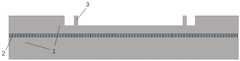
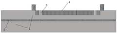
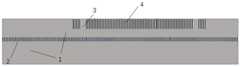
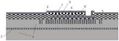
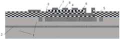
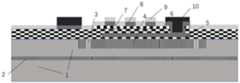
图1为基于FBAR的压力传感器制备方法流程示意图。Fig. 1 is a schematic flow chart of the FBAR-based pressure sensor preparation method.
图2为基于FBAR的压力传感器的制备步骤1)加工后的结构示意图;Fig. 2 is the structural representation after the preparation step 1) processing of the pressure sensor based on FBAR;
图3为基于FBAR的压力传感器的制备步骤2)加工后的结构示意图;Fig. 3 is the structural representation after the preparation step 2) processing of the pressure sensor based on FBAR;
图4为基于FBAR的压力传感器的制备步骤3)加工后的结构示意图;Fig. 4 is the structural schematic diagram after the preparation step 3) of the pressure sensor based on FBAR;
图5为基于FBAR的压力传感器的制备步骤4)加工后的结构示意图;Fig. 5 is the structural schematic diagram after the preparation step 4) of the pressure sensor based on FBAR;
图6为基于FBAR的压力传感器的制备步骤5)加工后的结构示意图;Fig. 6 is the structural schematic diagram after the preparation step 5) of the pressure sensor based on FBAR;
图7为基于FBAR的压力传感器的制备步骤6)加工后的结构示意图;Fig. 7 is the structural schematic diagram after the preparation step 6) of the FBAR-based pressure sensor;
图8为基于FBAR的压力传感器的制备步骤7)加工后的结构示意图;Fig. 8 is the structural representation after the preparation step 7) of the FBAR-based pressure sensor;
图9为基于FBAR的压力传感器的制备步骤8)加工后的结构示意图;FIG. 9 is a schematic structural view of the FBAR-based pressure sensor in the preparation step 8) after processing;
图10为基于FBAR的压力传感器的制备步骤9)加工后的结构示意图;FIG. 10 is a schematic structural view of the FBAR-based pressure sensor in the preparation step 9) after processing;
图11为基于FBAR的压力传感器的制备步骤10)加工后的结构示意图;FIG. 11 is a schematic structural view of the FBAR-based pressure sensor in the preparation step 10) after processing;
图12为基于FBAR的压力传感器的制备步骤11)加工后的结构示意图;FIG. 12 is a schematic structural view of the FBAR-based pressure sensor in the preparation step 11) after processing;
图13为基于FBAR的压力传感器的制备步骤12)加工后的结构示意图;FIG. 13 is a schematic structural view of the FBAR-based pressure sensor in the preparation step 12) after processing;
图14为基于FBAR的压力传感器的制备步骤13)加工后的结构示意图;FIG. 14 is a schematic structural view of the FBAR-based pressure sensor in the preparation step 13) after processing;
图15为基于FBAR的压力传感器的制备步骤14)加工后的结构示意图;FIG. 15 is a schematic structural view of the FBAR-based pressure sensor in the preparation step 14) after processing;
图16为基于FBAR的压力传感器的制备步骤15)加工后的结构示意图;FIG. 16 is a schematic structural view of the FBAR-based pressure sensor in the preparation step 15) after processing;
图17为基于FBAR的压力传感器的制备步骤16)加工后的结构示意图;FIG. 17 is a schematic structural view of the FBAR-based pressure sensor in the preparation step 16) after processing;
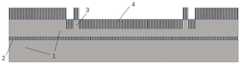
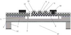
图18为基于FBAR的压力传感器的俯视结构图;Fig. 18 is a top view structural diagram of a pressure sensor based on FBAR;
图19为空气隙中无硅柱时的应力图;Figure 19 is a stress diagram when there is no silicon column in the air gap;
图20为空气隙中存在硅柱时的应力图;Figure 20 is a stress diagram when there are silicon pillars in the air gap;
其中,图中元件标识如下:Among them, the components in the figure are marked as follows:
1-衬底、2-二氧化硅绝缘层、3-硅柱、4-牺牲层、5-种子层、6-底电极、7-压电层、8-顶电极、9-钝化层、10-电势连接线、11-牺牲层释放孔、12-硬掩膜、13-背腔、14-空气隙。1-substrate, 2-silicon dioxide insulating layer, 3-silicon pillar, 4-sacrifice layer, 5-seed layer, 6-bottom electrode, 7-piezoelectric layer, 8-top electrode, 9-passivation layer, 10-potential connection line, 11-sacrificial layer release hole, 12-hard mask, 13-back cavity, 14-air gap.
具体实施方式detailed description
下面将结合本申请实施例中的附图,对本申请实施例中的技术方案进行清楚、完整地描述。显然,所描述的实施例仅仅是本申请一部分实施例,而不是全部的实施例。基于本申请中的实施例,本领域技术人员在没有作出创造性劳动前提下所获得的所有其他实施例,都属于本申请保护的范围。The technical solutions in the embodiments of the present application will be clearly and completely described below in conjunction with the drawings in the embodiments of the present application. Apparently, the described embodiments are only some of the embodiments of this application, not all of them. Based on the embodiments in this application, all other embodiments obtained by those skilled in the art without making creative efforts belong to the scope of protection of this application.
在本申请的描述中,需要理解的是,术语“第一”、“第二”仅用于描述目的,而不能理解为指示或暗示相对重要性或者隐含指明所指示的技术特征的数量。由此,限定有“第一”、“第二”的特征可以明示或者隐含地包括一个或者更多个所述特征。在本申请的描述中,“多个”的含义是两个或两个以上,除非另有明确具体的限定。In the description of the present application, it should be understood that the terms "first" and "second" are used for description purposes only, and cannot be interpreted as indicating or implying relative importance or implicitly indicating the quantity of indicated technical features. Thus, a feature defined as "first" or "second" may explicitly or implicitly include one or more of said features. In the description of the present application, "plurality" means two or more, unless otherwise specifically defined.
在本申请的描述中,需要说明的是,除非另有明确的规定和限定,术语“安装”、“相连”、“连接”应做广义理解,例如,可以是固定连接,也可以是可拆卸连接,或一体地连接;可以是机械连接,也可以是电连接或可以相互通讯;可以是直接相连,也可以通过中间媒介间接相连,可以是两个元件内部的连通或两个元件的相互作用关系。对于本领域的普通技术人员而言,可以根据具体情况理解上述术语在本申请中的具体含义。In the description of this application, it should be noted that unless otherwise specified and limited, the terms "installation", "connection", and "connection" should be understood in a broad sense, for example, it can be a fixed connection or a detachable connection. Connected, or integrally connected; it can be mechanically connected, or electrically connected, or can communicate with each other; it can be directly connected, or indirectly connected through an intermediary, and it can be the internal communication of two components or the interaction of two components relation. Those of ordinary skill in the art can understand the specific meanings of the above terms in this application according to specific situations.
下文的公开提供了许多不同的实施方式或例子用来实现本申请的不同结构。为了简化本申请的公开,下文中对特定例子的部件和设置进行描述。当然,它们仅仅为示例,并且目的不在于限制本申请。此外,本申请可以在不同例子中重复参考数字和/或参考字母,这种重复是为了简化和清楚的目的,其本身不指示所讨论各种实施方式和/或设置之间的关系。此外,本申请提供了的各种特定的工艺和材料的例子,但是本领域普通技术人员可以意识到其他工艺的应用和/或其他材料的使用。The following disclosure provides many different implementations or examples for implementing different structures of the present application. To simplify the disclosure of the present application, components and arrangements of specific examples are described below. Of course, they are examples only and are not intended to limit the application. Furthermore, the present application may repeat reference numerals and/or reference letters in various instances, such repetition is for simplicity and clarity and does not in itself indicate a relationship between the various embodiments and/or arrangements discussed. In addition, various specific process and material examples are provided herein, but one of ordinary skill in the art may recognize the use of other processes and/or the use of other materials.
实施例1Example 1
请参阅图17,本实施例中,一种基于FBAR的压力传感器,包括衬底1,该衬底1具有二氧化硅绝缘层2。在所述衬底1的底部,沉积有硬掩膜层12,并开有背腔13;在衬底顶部开有凹槽,凹槽内刻蚀有硅柱3;所述衬底上方沉积有种子层5,与所述衬底顶部凹槽包围形成空气隙14,优选地,所述种子层5材质采用AlN等,进一步的,种子层5的厚度约为200nm;所述种子层5上有压电振荡堆,所述压电振荡堆从下到上依次为底电极6、压电层7和顶电极8,所述的底电极沉积在所述种子层5上方,所述压电层7沉积在底电极6上方,所述顶电极8沉积在压电层7上方,其中压电层7中开有通孔,将部分底电极6露出,所述通孔处的底电极6区域上方和顶电极8部分区域上方沉积有电势连接线10,优选地,所述顶电极8和底电极6材质采用Mo等,进一步的,底电极6和顶电极8厚度均约为200nm,所述压电层7材质采用AlN或ScAlN,压电层厚度约为1μm,所述电势连接线10材质采用Au,厚度约为1μm;所述的压电振荡堆上方有钝化层9,所述钝化层9沉积在所述压电层7和所述顶电极8上方,所述电势连接线10上方不存在所述钝化层9,优选的,钝化层材质通常采用AlN,厚度约为100nm;在所述空气隙14上方的压电层7中,还刻蚀有释放孔11;Please refer to FIG. 17 , in this embodiment, a pressure sensor based on FBAR includes a
实施例2Example 2
请参阅图1~18,在实施例1的基础上,上述的一种基于FBAR的压力传感器的制备方法,包括刻蚀凹槽与硅柱、沉积牺牲层、去除顶部牺牲层、化学机械磨平、沉积种子层、沉积底电极、沉积压电层、制备底电极通孔、沉积顶电极、沉积钝化层、制备电势连接线、制备释放孔、沉积硬掩膜、背部凹槽释放和空气隙释放;具体包括以下步骤:Please refer to Figures 1-18. On the basis of Example 1, the above-mentioned FBAR-based pressure sensor preparation method includes etching grooves and silicon pillars, depositing a sacrificial layer, removing the top sacrificial layer, and chemical-mechanical grinding. , deposition of seed layer, deposition of bottom electrode, deposition of piezoelectric layer, preparation of via hole for bottom electrode, deposition of top electrode, deposition of passivation layer, preparation of potential connection line, preparation of release hole, deposition of hard mask, back groove relief and air gap Release; specifically include the following steps:
1)在具有二氧化硅绝缘层2的衬底1的顶面,刻蚀出一个凹槽,深度为3.5μm,凹槽内部刻蚀出多个硅柱3,硅柱高度为3.5μm;1) On the top surface of the
2)在衬底1的顶部和步骤1刻蚀出的凹槽内,沉积一层二氧化硅层,厚度为3.5μm;2) On the top of the
3)刻蚀掉SOI 1、2顶部沉积的二氧化硅,留下凹槽内的二氧化硅作为牺牲层4;3) Etching away the silicon dioxide deposited on the top of the
4)利用化学机械抛光(CMP)工艺去除由于光刻及刻蚀工艺误差所导致的SOI顶部表面残留的二氧化硅;4) Using a chemical mechanical polishing (CMP) process to remove residual silicon dioxide on the top surface of the SOI caused by photolithography and etching process errors;
5)在抛光后的衬底1的表面沉积一层厚度为0.2μm的AlN种子层5;5) Depositing an
6)在种子层上沉积一层厚度为200nm的Mo作为底电极6;6) Depositing a layer of Mo with a thickness of 200 nm on the seed layer as the
7)通过刻蚀将底电极6的图形化;7) patterning the
8)在底电极上一步刻蚀露出的种子层上沉积压电层7,压电层材料为AlN或ScAlN,厚度为1000nm;8) Depositing a
9)将压电层图形化,刻蚀出通孔,暴露出底电极6。9) Patterning the piezoelectric layer, etching through holes, and exposing the
10)在压电层上沉积一层厚度为200nm的Mo作为顶电极8,底电极通孔处和通孔壁上也需要沉积;10) Depositing a layer of Mo with a thickness of 200nm on the piezoelectric layer as the
11)通过刻蚀将顶电极8图形化;11) patterning the
12)在图形化后的顶电极8和露出的压电层7上沉积一层钝化层9,材料为AlN,并将钝化层9图形化,露出两侧的电极接口;12) Deposit a
13)利用解开-剥离工艺,在两侧露出的电极接口上沉积电势连接线10,材料为Au,厚度约为1000nm;13) Using the unraveling-stripping process, deposit
14)利用深反应离子刻蚀(DRIE),顶端刻蚀出一个释放孔11,露出牺牲层4;14) Using deep reactive ion etching (DRIE), etch a
15)在晶圆背部沉积一层Mo厚度约为200nm,利用Mo作为硬掩膜,先将底部Mo层刻蚀为硬掩膜板12,再将底部的SOI基底刻蚀掏空,露出埋氧层2,形成一个背腔13;15) Deposit a layer of Mo with a thickness of about 200nm on the back of the wafer. Using Mo as a hard mask, first etch the bottom Mo layer into a
16)利用步骤14)刻蚀出的释放孔11,注入刻蚀液将牺牲层4去除,释放出空气隙14,并保留空气隙内部的硅柱3。16) Using the
如图19与图20所示,可以明显看出,在图20压电振荡区边缘处应力值明显大于图19处对应位置的应力值,说明硅柱的存在导致了应力集中,进而提升了该传感器的灵敏度。As shown in Figure 19 and Figure 20, it can be clearly seen that the stress value at the edge of the piezoelectric oscillation area in Figure 20 is significantly greater than the stress value at the corresponding position in Figure 19, indicating that the existence of silicon pillars leads to stress concentration, thereby improving the Sensitivity of the sensor.
以上所述,仅为本申请较佳的具体实施方式,但本申请的保护范围并不局限于此,任何熟悉本技术领域的技术人员在本申请揭露的技术范围内,可轻易想到的变化或替换,都应涵盖在本申请的保护范围之内。The above is only a preferred embodiment of the present application, but the scope of protection of the present application is not limited thereto. Any person familiar with the technical field can easily conceive of changes or changes within the technical scope disclosed in this application Replacement should be covered within the protection scope of this application.
Claims (8)
Translated fromChinesePriority Applications (1)
| Application Number | Priority Date | Filing Date | Title |
|---|---|---|---|
| CN202211131706.2ACN115513365A (en) | 2022-09-16 | 2022-09-16 | A kind of pressure sensor based on FBAR and preparation method thereof |
Applications Claiming Priority (1)
| Application Number | Priority Date | Filing Date | Title |
|---|---|---|---|
| CN202211131706.2ACN115513365A (en) | 2022-09-16 | 2022-09-16 | A kind of pressure sensor based on FBAR and preparation method thereof |
Publications (1)
| Publication Number | Publication Date |
|---|---|
| CN115513365Atrue CN115513365A (en) | 2022-12-23 |
Family
ID=84525288
Family Applications (1)
| Application Number | Title | Priority Date | Filing Date |
|---|---|---|---|
| CN202211131706.2APendingCN115513365A (en) | 2022-09-16 | 2022-09-16 | A kind of pressure sensor based on FBAR and preparation method thereof |
Country Status (1)
| Country | Link |
|---|---|
| CN (1) | CN115513365A (en) |
Cited By (1)
| Publication number | Priority date | Publication date | Assignee | Title |
|---|---|---|---|---|
| CN120091753A (en)* | 2025-04-25 | 2025-06-03 | 广州市艾佛光通科技有限公司 | A BAW pressure sensor and its preparation method |
Citations (5)
| Publication number | Priority date | Publication date | Assignee | Title |
|---|---|---|---|---|
| US20030129785A1 (en)* | 2002-01-10 | 2003-07-10 | Barber Bradley Paul | Structurally supported thin film resonator and method of fabrication |
| US20100029031A1 (en)* | 2008-06-23 | 2010-02-04 | Commissariat A L'energie Atomique | Method of fabricating a mems/nems electromechanical component |
| CN108917991A (en)* | 2018-06-28 | 2018-11-30 | 武汉大学 | Highly sensitive piezoelectric mems sensor and preparation method thereof |
| CN112886939A (en)* | 2020-12-25 | 2021-06-01 | 杭州左蓝微电子技术有限公司 | Film bulk acoustic resonator, preparation method thereof and filter |
| CN114295256A (en)* | 2021-12-22 | 2022-04-08 | 苏州航凯微电子技术有限公司 | Pressure sensor based on FBAR structure and preparation method thereof |
- 2022
- 2022-09-16CNCN202211131706.2Apatent/CN115513365A/enactivePending
Patent Citations (5)
| Publication number | Priority date | Publication date | Assignee | Title |
|---|---|---|---|---|
| US20030129785A1 (en)* | 2002-01-10 | 2003-07-10 | Barber Bradley Paul | Structurally supported thin film resonator and method of fabrication |
| US20100029031A1 (en)* | 2008-06-23 | 2010-02-04 | Commissariat A L'energie Atomique | Method of fabricating a mems/nems electromechanical component |
| CN108917991A (en)* | 2018-06-28 | 2018-11-30 | 武汉大学 | Highly sensitive piezoelectric mems sensor and preparation method thereof |
| CN112886939A (en)* | 2020-12-25 | 2021-06-01 | 杭州左蓝微电子技术有限公司 | Film bulk acoustic resonator, preparation method thereof and filter |
| CN114295256A (en)* | 2021-12-22 | 2022-04-08 | 苏州航凯微电子技术有限公司 | Pressure sensor based on FBAR structure and preparation method thereof |
Non-Patent Citations (1)
| Title |
|---|
| KAMOHARA T, AKIYAMA M, UENO N, ET AL.: "Growth of highly c-axis-oriented aluminum nitride thin films on molybdenum electrodes using aluminum nitride interlayers", 1-8, vol. 275, 19 January 2005 (2005-01-19), pages 6* |
Cited By (2)
| Publication number | Priority date | Publication date | Assignee | Title |
|---|---|---|---|---|
| CN120091753A (en)* | 2025-04-25 | 2025-06-03 | 广州市艾佛光通科技有限公司 | A BAW pressure sensor and its preparation method |
| CN120091753B (en)* | 2025-04-25 | 2025-08-05 | 广州市艾佛光通科技有限公司 | A BAW pressure sensor and its preparation method |
Similar Documents
| Publication | Publication Date | Title |
|---|---|---|
| CN101449347B (en) | Capacitive micro- electro-mechanical sensors with single crystal silicon electrodes | |
| JP4144640B2 (en) | Method for manufacturing vibration sensor | |
| US8643129B2 (en) | MEMS device | |
| CN110550598B (en) | Resonant differential pressure sensor and preparation method thereof | |
| US20140016798A1 (en) | Mems device | |
| CN103234567B (en) | MEMS (micro-electromechanical systems) capacitive ultrasonic sensor on basis of anodic bonding technology | |
| CN114577370B (en) | High-precision flange plate type silicon resonance pressure sensor and manufacturing process thereof | |
| JP2007184931A (en) | Vacuum packaged single crystal silicon device | |
| JP2006205352A (en) | Method for manufacturing MEMS structure | |
| CN111491244B (en) | MEMS microphone processing method and MEMS microphone | |
| CN111174951A (en) | Piezoelectric sensor and method of making the same | |
| US6930366B2 (en) | Method for forming a cavity structure on SOI substrate and cavity structure formed on SOI substrate | |
| CN108931321A (en) | Beam-island-film integration resonant mode pressure sensor structure and manufacturing method | |
| JP2000065665A (en) | Micromachine sensor and method for manufacturing the sensor | |
| CN115513365A (en) | A kind of pressure sensor based on FBAR and preparation method thereof | |
| JP2008517523A (en) | Silicon microphone | |
| JP3536817B2 (en) | Semiconductor dynamic quantity sensor and method of manufacturing the same | |
| CN115752818B (en) | Resonant pressure sensor and manufacturing method thereof | |
| JP2008271568A (en) | Vibration sensor | |
| CN103323042A (en) | Capacitance-type ultrasonic sensor of integrated full-vibration conductive film structure and manufacturing method thereof | |
| CN116462153A (en) | Monolithic integrated MEMS pressure and acceleration composite sensor and preparation method thereof | |
| US11511990B2 (en) | Method for manufacturing a microelectronic device comprising a membrane suspended above a cavity | |
| CN210694353U (en) | A MEMS structure | |
| KR102067996B1 (en) | Silicon nanowire-based piezoresistive microphone and method of manufacturing the same | |
| CN120440830A (en) | Vacuum packaging technology for realizing planar interconnection and polycrystalline silicon-glass anode bonding |
Legal Events
| Date | Code | Title | Description |
|---|---|---|---|
| PB01 | Publication | ||
| PB01 | Publication | ||
| SE01 | Entry into force of request for substantive examination | ||
| SE01 | Entry into force of request for substantive examination |