CN115513024A - ICP etching device and using method thereof - Google Patents
ICP etching device and using method thereofDownload PDFInfo
- Publication number
- CN115513024A CN115513024ACN202110697725.0ACN202110697725ACN115513024ACN 115513024 ACN115513024 ACN 115513024ACN 202110697725 ACN202110697725 ACN 202110697725ACN 115513024 ACN115513024 ACN 115513024A
- Authority
- CN
- China
- Prior art keywords
- power supply
- plasma
- radio frequency
- bias
- excitation
- Prior art date
- Legal status (The legal status is an assumption and is not a legal conclusion. Google has not performed a legal analysis and makes no representation as to the accuracy of the status listed.)
- Pending
Links
- 238000000034methodMethods0.000titleclaimsabstractdescription32
- 238000005530etchingMethods0.000titleclaimsabstractdescription28
- 238000006243chemical reactionMethods0.000claimsabstractdescription55
- 230000005284excitationEffects0.000claimsabstractdescription47
- 238000004140cleaningMethods0.000claimsabstractdescription26
- 230000008878couplingEffects0.000claimsabstractdescription22
- 238000010168coupling processMethods0.000claimsabstractdescription22
- 238000005859coupling reactionMethods0.000claimsabstractdescription22
- 239000007795chemical reaction productSubstances0.000claimsabstractdescription10
- 230000002093peripheral effectEffects0.000claimsdescription12
- 230000001939inductive effectEffects0.000claimsdescription4
- 238000004891communicationMethods0.000claimsdescription2
- 238000005086pumpingMethods0.000claims3
- 235000012431wafersNutrition0.000claims2
- 230000005684electric fieldEffects0.000abstractdescription8
- 230000000694effectsEffects0.000abstractdescription6
- 230000008021depositionEffects0.000abstractdescription4
- 238000004519manufacturing processMethods0.000abstractdescription4
- 239000004065semiconductorSubstances0.000abstractdescription2
- 230000001965increasing effectEffects0.000description11
- 239000007789gasSubstances0.000description9
- 230000008569processEffects0.000description9
- 238000009616inductively coupled plasmaMethods0.000description8
- 239000000463materialSubstances0.000description6
- 238000011109contaminationMethods0.000description3
- 238000001312dry etchingMethods0.000description3
- MCMNRKCIXSYSNV-UHFFFAOYSA-NZirconium dioxideChemical compoundO=[Zr]=OMCMNRKCIXSYSNV-UHFFFAOYSA-N0.000description2
- 230000002708enhancing effectEffects0.000description2
- 230000006872improvementEffects0.000description2
- 239000002184metalSubstances0.000description2
- 229910052751metalInorganic materials0.000description2
- 239000002245particleSubstances0.000description2
- 229910001030Iron–nickel alloyInorganic materials0.000description1
- 230000009471actionEffects0.000description1
- PNEYBMLMFCGWSK-UHFFFAOYSA-Naluminium oxideInorganic materials[O-2].[O-2].[O-2].[Al+3].[Al+3]PNEYBMLMFCGWSK-UHFFFAOYSA-N0.000description1
- 239000003990capacitorSubstances0.000description1
- 230000008859changeEffects0.000description1
- 229910052593corundumInorganic materials0.000description1
- 239000003989dielectric materialSubstances0.000description1
- CJNBYAVZURUTKZ-UHFFFAOYSA-Nhafnium(IV) oxideInorganic materialsO=[Hf]=OCJNBYAVZURUTKZ-UHFFFAOYSA-N0.000description1
- 230000010354integrationEffects0.000description1
- 150000002500ionsChemical class0.000description1
- 229910052741iridiumInorganic materials0.000description1
- 238000009832plasma treatmentMethods0.000description1
- 229910052697platinumInorganic materials0.000description1
- 229910052707rutheniumInorganic materials0.000description1
- 238000005728strengtheningMethods0.000description1
- 229910001845yogo sapphireInorganic materials0.000description1
Images

Classifications
- H—ELECTRICITY
- H01—ELECTRIC ELEMENTS
- H01J—ELECTRIC DISCHARGE TUBES OR DISCHARGE LAMPS
- H01J37/00—Discharge tubes with provision for introducing objects or material to be exposed to the discharge, e.g. for the purpose of examination or processing thereof
- H01J37/32—Gas-filled discharge tubes
- H01J37/32431—Constructional details of the reactor
- H01J37/32798—Further details of plasma apparatus not provided for in groups H01J37/3244 - H01J37/32788; special provisions for cleaning or maintenance of the apparatus
- H01J37/32853—Hygiene
- H01J37/32862—In situ cleaning of vessels and/or internal parts
- H—ELECTRICITY
- H01—ELECTRIC ELEMENTS
- H01J—ELECTRIC DISCHARGE TUBES OR DISCHARGE LAMPS
- H01J37/00—Discharge tubes with provision for introducing objects or material to be exposed to the discharge, e.g. for the purpose of examination or processing thereof
- H01J37/32—Gas-filled discharge tubes
- H01J37/32009—Arrangements for generation of plasma specially adapted for examination or treatment of objects, e.g. plasma sources
- H01J37/32082—Radio frequency generated discharge
- H01J37/32174—Circuits specially adapted for controlling the RF discharge
- H01J37/32183—Matching circuits
- H—ELECTRICITY
- H01—ELECTRIC ELEMENTS
- H01L—SEMICONDUCTOR DEVICES NOT COVERED BY CLASS H10
- H01L21/00—Processes or apparatus adapted for the manufacture or treatment of semiconductor or solid state devices or of parts thereof
- H01L21/67—Apparatus specially adapted for handling semiconductor or electric solid state devices during manufacture or treatment thereof; Apparatus specially adapted for handling wafers during manufacture or treatment of semiconductor or electric solid state devices or components ; Apparatus not specifically provided for elsewhere
- H01L21/67005—Apparatus not specifically provided for elsewhere
- H01L21/67011—Apparatus for manufacture or treatment
- H01L21/67017—Apparatus for fluid treatment
- H01L21/67063—Apparatus for fluid treatment for etching
- H01L21/67069—Apparatus for fluid treatment for etching for drying etching
Landscapes
- Engineering & Computer Science (AREA)
- Physics & Mathematics (AREA)
- Plasma & Fusion (AREA)
- Chemical & Material Sciences (AREA)
- Analytical Chemistry (AREA)
- Epidemiology (AREA)
- Health & Medical Sciences (AREA)
- Public Health (AREA)
- Condensed Matter Physics & Semiconductors (AREA)
- General Physics & Mathematics (AREA)
- Manufacturing & Machinery (AREA)
- Computer Hardware Design (AREA)
- Microelectronics & Electronic Packaging (AREA)
- Power Engineering (AREA)
- Drying Of Semiconductors (AREA)
Abstract
Description
Translated fromChinese技术领域technical field
本发明涉及半导体芯片生产设备技术领域,尤其涉及一种ICP刻蚀装置及其使用方法。The invention relates to the technical field of semiconductor chip production equipment, in particular to an ICP etching device and a method for using the same.
背景技术Background technique
目前Pt、Ru、Ir、NiFe、Au等非挥发性材料主要通过电感耦合等离子体(ICP)进行干法刻蚀。电感耦合等离子通常由置于等离子体处理腔室外部与电介质窗相邻的线圈产生,腔室内的工艺气体被点燃后形成等离子体。在对非挥发性材料的干法刻蚀工艺过程中,由于反应产物的蒸汽压较低,难以被真空泵抽走,导致反应产物沉积在电介质窗和其他等离子体处理腔室内壁上沉积。这不仅会产生颗粒沾污,也会导致工艺随时间漂移使工艺过程的重复性下降。因此需要对等离子体处理腔室进行清洗。但是在实际使用过程中,清洗将导致工艺中断,降低等离子体处理设备的生产效率。At present, non-volatile materials such as Pt, Ru, Ir, NiFe, and Au are mainly dry-etched by inductively coupled plasma (ICP). Inductively coupled plasma is typically generated by coils placed outside the plasma processing chamber adjacent to the dielectric window, and process gases within the chamber are ignited to form the plasma. During the dry etching process of non-volatile materials, due to the low vapor pressure of the reaction product, it is difficult to be pumped away by the vacuum pump, resulting in the deposition of the reaction product on the dielectric window and other inner walls of the plasma processing chamber. This not only creates particle contamination, but also causes the process to drift over time, making the process less repeatable. Therefore, it is necessary to clean the plasma processing chamber. However, in actual use, cleaning will cause process interruption and reduce the production efficiency of plasma processing equipment.
随着近年来第三代存储器——磁存储器(MRAM)的不断发展和集成度的不断提高,对金属栅极材料(如Model、Ta等)和高k栅介质材料(如Al2O3、HfO2和ZrO2等)等新型非挥发性材料的干法刻蚀需求不断增加,解决非挥发性材料在干法刻蚀过程中产生的侧壁沉积和颗粒沾污,同时提高等离子体处理腔室的清洗工艺效率是十分必要的。With the continuous development and integration of the third generation of memory - magnetic memory (MRAM) in recent years, metal gate materials (such as Model, Ta, etc.) and high-k gate dielectric materials (such as Al2O3, HfO2 and ZrO2 etc.) The demand for dry etching of new non-volatile materials continues to increase, to solve the sidewall deposition and particle contamination of non-volatile materials during dry etching, and to improve the cleaning process efficiency of the plasma processing chamber is very necessary.
目前已有的清洗方法是在射频线圈与介质窗之间放置一个法拉第平板,通过在法拉第平板上加射频功率的方法去清洗介质窗及侧壁。当进行金属刻蚀时,射频功率经过线圈耦合入腔室进行等离子体处理。当需要清洗介质窗及侧壁时,射频功率经过法拉第平板耦合入腔室(两种模式由三通开关切换)。从而实现对介质窗及侧壁的清洗,虽热目前这种方法可以实现对介质窗及侧壁的清洗,但效率并不是很高,从而影响产能。The existing cleaning method is to place a Faraday plate between the radio frequency coil and the dielectric window, and to clean the dielectric window and the side wall by applying radio frequency power to the Faraday plate. When performing metal etching, RF power is coupled into the chamber via coils for plasma processing. When it is necessary to clean the dielectric window and the side wall, the RF power is coupled into the chamber through the Faraday plate (the two modes are switched by the three-way switch). Thereby, the cleaning of the medium window and the side wall can be realized. Although the current method can realize the cleaning of the medium window and the side wall, the efficiency is not very high, thereby affecting the production capacity.
发明内容Contents of the invention
本发明的目的是为了解决现有技术中存在的缺点,而提出一种ICP刻蚀装置及其使用方法。The purpose of the present invention is to provide an ICP etching device and its usage method in order to solve the shortcomings in the prior art.
为了实现上述目的,本发明采用了如下技术方案:In order to achieve the above object, the present invention adopts the following technical solutions:
一种ICP刻蚀装置,包括:An ICP etching device, comprising:
反应腔体,所述反应腔体限定出等离子体反应腔;a reaction chamber defining a plasma reaction chamber;
介质窗,所述介质窗被构造成所述等离子体反应腔的顶壁;a dielectric window configured as a top wall of the plasma reaction chamber;
法拉第平板和射频线圈,所述法拉第平板铺设在所述介质窗上,所述射频线圈临近所述法拉第平板的上表面设置;a Faraday plate and a radio frequency coil, the Faraday plate is laid on the dielectric window, and the radio frequency coil is arranged adjacent to the upper surface of the Faraday plate;
第一射频电源,所述第一射频电源通过第一匹配网络和所述射频线圈或法拉第平板相连,用以将通入所述等离子体反应腔内的气体电离产生等离子体;A first radio frequency power supply, the first radio frequency power supply is connected to the radio frequency coil or the Faraday plate through a first matching network, and is used to ionize the gas passing into the plasma reaction chamber to generate plasma;
电极,所述电极设在所述等离子体反应腔内,所述电极上承载有晶圆;an electrode, the electrode is arranged in the plasma reaction chamber, and a wafer is carried on the electrode;
第二射频电源,所述第二射频电源通过第二匹配网络和所述电极相连,用以将通入所述反应腔室内的气体电离产生等离子体;a second radio frequency power supply, the second radio frequency power supply is connected to the electrode through a second matching network, and is used to ionize the gas flowing into the reaction chamber to generate plasma;
在所述第一射频电源接通且在所述反应腔室内产生稳定的等离子体后,再接通所述第二射频电源,所述第一射频电源和所述第二射频电源共同作用在所述反应腔室内周壁和所述介质窗下表面上,用以对所述反应腔室内周壁和所述介质窗下表面进行清洗。After the first radio frequency power supply is turned on and a stable plasma is generated in the reaction chamber, the second radio frequency power supply is turned on, and the first radio frequency power supply and the second radio frequency power supply work together on the The inner peripheral wall of the reaction chamber and the lower surface of the medium window are used to clean the inner peripheral wall of the reaction chamber and the lower surface of the medium window.
作为更进一步的优选方案,第一射频电源为激励射频电源,所述第二射频电源为偏压射频电源。As a further preferred solution, the first RF power supply is an excitation RF power supply, and the second RF power supply is a bias RF power supply.
作为更进一步的优选方案,法拉第平板由多个形状结构呈中心对称式布置,所述多个形状结构之间具有间隙。As a further preferred solution, the Faraday plate consists of a plurality of shape structures arranged symmetrically about the center, and there are gaps between the plurality of shape structures.
作为更进一步的优选方案,抽真空装置和所述反应腔室相连通,所述抽真空装置包括压力控制阀和真空泵,所述压力控制阀连接在真空泵和所述反应腔体之间。As a further preferred solution, the vacuuming device is in communication with the reaction chamber, the vacuuming device includes a pressure control valve and a vacuum pump, and the pressure control valve is connected between the vacuum pump and the reaction chamber.
一种ICP刻蚀装置的使用方法,包括以下步骤:A method for using an ICP etching device, comprising the following steps:
步骤一:开始刻蚀时,接通所述激励射频电源和所述射频线圈,通过电感耦合的方式对通入所述等离子体反应腔内的气体电离产生等离子体,同时接通所述偏压射频电源和所述电极,用以提供偏置电压,以对所述等离子体反应腔内的晶圆进行刻蚀;Step 1: When starting etching, turn on the excitation radio frequency power supply and the radio frequency coil, ionize the gas passing into the plasma reaction chamber by inductive coupling to generate plasma, and turn on the bias voltage at the same time A radio frequency power supply and the electrodes are used to provide a bias voltage to etch the wafer in the plasma reaction chamber;
步骤二:当刻蚀完成后,断开所述激励射频电源和所述偏压射频电源;Step 2: After the etching is completed, disconnect the excitation RF power supply and the bias RF power supply;
步骤三:此时所述介质窗下表面以及所述等离子体反应腔内周壁均沉积有反应产物,需要清洗时,再次开启所述激励射频电源,经第一匹配网络给法拉第平板通电,通过电容耦合的方式产生将通入等离子体反应腔内的气体电离产生等离子体,提供鞘层电压;Step 3: At this time, reaction products are deposited on the lower surface of the dielectric window and the inner peripheral wall of the plasma reaction chamber. When cleaning is required, the excitation RF power supply is turned on again, and the Faraday plate is energized through the first matching network. Coupling produces ionization of the gas that passes into the plasma reaction chamber to generate plasma and provides sheath voltage;
步骤四:当所述等离子体反应腔内产生稳定的等离子体后,再次开启偏压射频电源,偏压射频电源经过第二匹配网络以电容耦合的方式产生等离子体,提供鞘层电压;在两种所提供的鞘层电压共同作用在所述介质窗上及所述等离子体反应腔的内周壁,进而对所述介质窗内顶壁上及所述等离子体反应腔的内侧壁上沉积反应产物进行清洗。Step 4: After stable plasma is generated in the plasma reaction chamber, the bias RF power supply is turned on again, and the bias RF power supply generates plasma in a capacitive coupling manner through the second matching network to provide the sheath voltage; The provided sheath voltage acts together on the dielectric window and the inner peripheral wall of the plasma reaction chamber, and then deposits the reaction product on the inner top wall of the dielectric window and the inner wall of the plasma reaction chamber Clean up.
作为更进一步的优选方案,步骤三和所述步骤四中,激励射频电源和偏压射频电源再次开启后的功率为从小到大逐渐开启。As a further preferred solution, in Step 3 and Step 4, after the excitation RF power supply and the bias RF power supply are turned on again, the power is gradually turned on from small to large.
作为更进一步的优选方案,激励射频电源和偏压射频电源的频率均为13.56MHz。As a further preferred solution, the frequencies of the excitation RF power supply and the bias RF power supply are both 13.56 MHz.
作为更进一步的优选方案,步骤三和所述步骤四中,清洗效率可以通过激励射频电源和偏压射频电源的相位差来进行调整,且调整范围为0°-360°;相位差调整至180°时,射频电压达到最大值,此时叠加的鞘层电场强度最高,等离子体对腔室侧壁及介质窗表面的轰击效果最强,清洗效率最高。As a further preferred solution, in step 3 and step 4, the cleaning efficiency can be adjusted by the phase difference between the excitation RF power supply and the bias RF power supply, and the adjustment range is 0°-360°; the phase difference is adjusted to 180° °, the RF voltage reaches the maximum value, at this time the superimposed sheath electric field intensity is the highest, the plasma has the strongest bombardment effect on the chamber side wall and the surface of the dielectric window, and the cleaning efficiency is the highest.
作为更进一步的优选方案,相位差调整方法可以是,固定激励射频电源的相位,调整第二偏压射频电源的相位,直至达到所需相位差。As a further preferred solution, the phase difference adjustment method may be to fix the phase of the exciting RF power supply and adjust the phase of the second bias RF power supply until the required phase difference is reached.
作为更进一步的优选方案,相位差调整方法可以是,固定偏压电源相位,调整激励电源相位至所需相位差;还可以是激励电源与偏压电源同时调整至所需相位差。As a further preferred solution, the phase difference adjustment method may be to fix the phase of the bias power supply and adjust the phase of the excitation power supply to the required phase difference; it may also be to adjust the excitation power supply and the bias power supply to the required phase difference at the same time.
本发明通过两个电容耦合结构的叠加,它们所产生的鞘层电场强度就会叠加,从而加强了等离子体对介质窗及侧壁的轰击效果,实现对沉积反应产物的清洗。In the present invention, through the superposition of two capacitive coupling structures, the electric field strength of the sheath layer generated by them will be superimposed, thereby strengthening the bombardment effect of the plasma on the dielectric window and the side wall, and realizing the cleaning of deposition reaction products.
附图说明Description of drawings
图1为本发明刻蚀装置的结构示意图;Fig. 1 is the structural representation of etching device of the present invention;
图2为激励电源与偏压电源的相位差与射频电压的关系图。Fig. 2 is a graph showing the relationship between the phase difference between the excitation power supply and the bias power supply and the radio frequency voltage.
具体实施方式detailed description
下面将结合本发明实施例中的附图,对本发明实施例中的技术方案进行清楚、完整地描述,显然,所描述的实施例仅仅是本发明一部分实施例,而不是全部的实施例。The following will clearly and completely describe the technical solutions in the embodiments of the present invention with reference to the accompanying drawings in the embodiments of the present invention. Obviously, the described embodiments are only some, not all, embodiments of the present invention.
本发明所应用的ICP刻蚀装置,包括:The ICP etching device applied in the present invention includes:
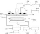
反应腔体,所述反应腔体限定出等离子体反应腔102;a reaction chamber, the reaction chamber defines a
介质窗110,所述介质窗110被构造成所述等离子体反应腔102的顶壁;a
法拉第平板160和射频线圈108,所述法拉第平板160铺设在所述介质窗110上,所述射频线圈108临近所述法拉第平板160的上表面设置;A Faraday
第一射频电源,所述第一射频电源通过第一匹配网络106和所述射频线圈108或法拉第平板160相连,用以将通入所述等离子体反应腔102内的气体电离产生等离子体112;A first radio frequency power supply, the first radio frequency power supply is connected to the
此处通过三通开关150进行调节,三通开关150安装于第一匹配网络106,可则一切换至连接射频线圈108的线路或者连接法拉第平板160的线路;The three-
电极118,所述电极118设在所述等离子体反应腔102内,所述电极118上承载有晶圆;An
第二射频电源,所述第二射频电源通过第二匹配网络116和所述电极118相连,用以将通入所述反应腔室内的气体电离产生等离子体;The second radio frequency power supply, the second radio frequency power supply is connected to the
在第一射频电源接通且在所述反应腔室内产生稳定的等离子体后,再接通第二射频电源,第一射频电源和第二射频电源共同作用在所述反应腔室内周壁和所述介质窗110下表面上,用以对所述反应腔室内周壁和所述介质窗110下表面进行清洗。After the first radio frequency power supply is turned on and a stable plasma is generated in the reaction chamber, the second radio frequency power supply is turned on, and the first radio frequency power supply and the second radio frequency power supply work together on the inner peripheral wall of the reaction chamber and the The lower surface of the
为了进一步提高MRAM材料在刻蚀过程中介质窗及侧壁沾污的清洗效率,本发明提出了一种两套射频源同频同步工作的一种清洗办法。这种方法可以增强鞘层电场强度,从而加强等离子体对介质窗及侧壁的轰击效果,实现了清洗效率的提高。两套射频源及匹配网络,一套与法拉第平板相连,与放置晶圆的电极构成电容极板的两极,实现以电容耦合的方式去加工等离子体。另一套与放置晶圆的电极相连,这时放置晶圆的电极与放置法拉第平板的介质窗构成了另一套电容结构,也实现了用电容耦合的方式去加工等离子体。两个电容耦合结构的叠加,它们所产生的鞘层电场强度就会叠加,从而加强了等离子体对介质窗及侧壁的轰击效果,这就实现了清洗效率的提高。叠加后鞘层电场强度的大小由两个同频电源的相位差决定。In order to further improve the cleaning efficiency of the dielectric window and side wall contamination of the MRAM material during the etching process, the present invention proposes a cleaning method in which two sets of radio frequency sources work synchronously at the same frequency. This method can enhance the electric field intensity of the sheath, thereby enhancing the bombardment effect of the plasma on the dielectric window and the side wall, and realizing the improvement of the cleaning efficiency. Two sets of RF sources and matching networks, one of which is connected to the Faraday plate, forms the two poles of the capacitive plate with the electrode on which the wafer is placed, and realizes plasma processing by capacitive coupling. The other set is connected to the electrode on which the wafer is placed. At this time, the electrode on which the wafer is placed and the dielectric window on which the Faraday plate is placed form another capacitive structure, which also realizes plasma processing by capacitive coupling. With the superposition of the two capacitive coupling structures, the electric field strength of the sheath layer generated by them will be superimposed, thereby enhancing the bombardment effect of the plasma on the dielectric window and the side wall, thereby improving the cleaning efficiency. The magnitude of the electric field strength of the sheath after superposition is determined by the phase difference of the two power sources with the same frequency.
具体的说,当需要刻蚀时,将激励电源功率加到线圈上通过电感耦合的方式产生等离子体,偏压电源通过电容耦合的方式为等离子体提供偏置电压,实现对晶圆的刻蚀。当需要清洗时,将激励射频电源功率加到法拉第平板上,此时法拉第平板与放置晶圆的电极构成电容的两极,经过电容耦合方式产生等离子体,在鞘层电场强度的作用下来轰击腔室侧壁及介质窗表面。偏压电源经过匹配网络与放置晶圆的电极相连,同样经过电容耦合的方式加工等离子体,为侧壁及介质窗及提供鞘层电压。两个鞘层的叠加实现了清洗效率的提高。Specifically, when etching is required, the power of the excitation power supply is added to the coil to generate plasma through inductive coupling, and the bias power supply provides a bias voltage for the plasma through capacitive coupling to realize etching of the wafer. . When cleaning is required, the power of the excitation RF power supply is added to the Faraday plate. At this time, the Faraday plate and the electrode on which the wafer are placed form the two poles of the capacitor. The plasma is generated by capacitive coupling and bombards the chamber under the action of the electric field strength of the sheath. Side walls and dielectric window surfaces. The bias power supply is connected to the electrode on which the wafer is placed through a matching network, and the plasma is also processed through capacitive coupling to provide sheath voltage for the side wall and dielectric window. The superposition of the two sheath layers realizes the improvement of cleaning efficiency.
本发明的ICP刻蚀装置的使用方法,包括以下步骤:The using method of ICP etching device of the present invention comprises the following steps:
步骤一:开始刻蚀时,接通所述激励射频电源104和所述射频线圈108,通过电感耦合的方式对通入所述等离子体反应腔102内的气体电离产生等离子体112,同时接通所述偏压射频电源114和所述电极118,用以提供偏置电压,以对所述等离子体反应腔102内的晶圆进行刻蚀;Step 1: when starting etching, turn on the excitation radio
步骤二:当刻蚀完成后,断开所述激励射频电源104和所述偏压射频电源114;Step 2: After the etching is completed, disconnect the excitation
步骤三:此时所述介质窗110下表面以及所述等离子体反应腔102内周壁均沉积有反应产物,需要清洗时,再次开启所述激励射频电源104,经第一匹配网络106给法拉第平板160通电,通过电容耦合的方式产生将通入等离子体反应腔102内的气体电离产生等离子体112,提供鞘层电压;Step 3: At this time, reaction products are deposited on the lower surface of the
步骤四:当所述等离子体反应腔102内产生稳定的等离子体112后,再次开启偏压射频电源114,偏压射频电源114经过第二匹配网络116以电容耦合的方式产生等离子体112,提供鞘层电压;在两种所提供的鞘层电压共同作用在所述介质窗110上及所述等离子体反应腔102的内周壁,进而对所述介质窗110内顶壁上及所述等离子体反应腔102的内侧壁上沉积反应产物进行清洗。Step 4: After
清洗采用容性耦合的方式进行,射频电源提供的电压越高,所对应的鞘层电压就越高,鞘层电压越高,离子轰击介质窗表面的能量就变强,从而实现更高效率的清洗。实测当激励电源与偏压相位差为180°时,射频电压达到最大值。Cleaning is carried out by capacitive coupling. The higher the voltage provided by the RF power supply, the higher the corresponding sheath voltage. The higher the sheath voltage, the stronger the energy of ions bombarding the surface of the dielectric window, thereby achieving higher efficiency. cleaning. It is measured that when the phase difference between the excitation power supply and the bias voltage is 180°, the RF voltage reaches the maximum value.
其中,激励射频电源104和偏压射频电源114再次开启后的功率为从小到大逐渐开启。激励射频电源104和偏压射频电源114的频率均为13.56MHz。Wherein, the powers of the exciting
步骤三和所述步骤四中,清洗效率可以通过激励射频电源104和偏压射频电源114的相位差来进行调整,且调整范围为0°-360°;当相位差调整至180°时,射频电压达到最大值,此时叠加的鞘层电场强度最高,等离子体对腔室侧壁及介质窗表面的轰击效果最强,清洗效率最高。具体的说,如果要实现清洗效率最大化,就需要调整两套电源相位差至180°。可以使激励源源0°相位,偏压电源180°相位。也可以是激励电源30°相位,偏压电源210°相位。也可是激励电源180°相位,偏压电源0°相位等。满足两套电源相位差180°即可In Step 3 and Step 4, the cleaning efficiency can be adjusted by the phase difference between the excitation
相位差调整方法可以是,固定激励射频电源的相位,调整第二偏压射频电源114的相位,直至达到所需相位差。相位差调整方法可以是,固定偏压电源相位,调整激励电源相位至所需相位差 ;还可以是激励电源与偏压电源同时调整至所需相位差。The phase difference adjustment method may be to fix the phase of the exciting RF power supply and adjust the phase of the second bias
需要清洗时两套电源启辉顺序可以是先用激励电源启辉,待等离子体稳定后,再开启偏压电源。也可以是先用偏压电源启辉,待等离子体稳定后,在开启激励电源。When cleaning is required, the ignition sequence of the two sets of power supplies can be to use the excitation power supply first, and then turn on the bias power supply after the plasma is stabilized. It is also possible to use the bias power to start the ignition first, and then turn on the excitation power after the plasma is stabilized.
功率升高顺序可以是射频激励源功率与偏压电源功率交替上升,也可以是先升高射频激励源功率到所需功率,再升高偏压电源功率。也可以是先升高偏压电源功率至所需功率,再升高激励电源功率。The power increasing sequence may be that the power of the radio frequency excitation source and the power of the bias power supply are increased alternately, or that the power of the radio frequency excitation source is first increased to the required power, and then the power of the bias power supply is increased. It is also possible to increase the power of the bias power supply to the required power first, and then increase the power of the excitation power supply.
一般来说等离子体处理过程中,为了防止打火,点火步功率一般较小,当小功率点起来后再进行功率提高到所需的大功率,所以就存在功率提升的过程。如果激励电源和偏压电源同时提升可能导致等离子体不稳定,甚至灭辉,所以采用了分开升高功率。功率升高顺序可以是射频激励源功率与偏压电源功率交替上升,也可以是先升高射频激励源功率到所需功率,再升高偏压电源功率。也可以是先升高偏压电源功率至所需功率,再升高激励电源功率。Generally speaking, in the process of plasma treatment, in order to prevent sparking, the power of the ignition step is generally small. After the low power is turned on, the power is increased to the required high power, so there is a process of power increase. If the excitation power supply and the bias power supply are increased at the same time, the plasma may be unstable or even extinguished, so the power is increased separately. The power increasing sequence may be that the power of the radio frequency excitation source and the power of the bias power supply are increased alternately, or that the power of the radio frequency excitation source is first increased to the required power, and then the power of the bias power supply is increased. It is also possible to increase the power of the bias power supply to the required power first, and then increase the power of the excitation power supply.
以上所述,仅为本发明较佳的具体实施方式,但本发明的保护范围并不局限于此,任何熟悉本技术领域的技术人员在本发明揭露的技术范围内,根据本发明的技术方案及其发明构思加以等同替换或改变,都应涵盖在本发明的保护范围之内。The above is only a preferred embodiment of the present invention, but the scope of protection of the present invention is not limited thereto, any person familiar with the technical field within the technical scope disclosed in the present invention, according to the technical solution of the present invention Any equivalent replacement or change of the inventive concepts thereof shall fall within the protection scope of the present invention.
Claims (10)
Priority Applications (1)
| Application Number | Priority Date | Filing Date | Title |
|---|---|---|---|
| CN202110697725.0ACN115513024A (en) | 2021-06-23 | 2021-06-23 | ICP etching device and using method thereof |
Applications Claiming Priority (1)
| Application Number | Priority Date | Filing Date | Title |
|---|---|---|---|
| CN202110697725.0ACN115513024A (en) | 2021-06-23 | 2021-06-23 | ICP etching device and using method thereof |
Publications (1)
| Publication Number | Publication Date |
|---|---|
| CN115513024Atrue CN115513024A (en) | 2022-12-23 |
Family
ID=84499994
Family Applications (1)
| Application Number | Title | Priority Date | Filing Date |
|---|---|---|---|
| CN202110697725.0APendingCN115513024A (en) | 2021-06-23 | 2021-06-23 | ICP etching device and using method thereof |
Country Status (1)
| Country | Link |
|---|---|
| CN (1) | CN115513024A (en) |
Cited By (1)
| Publication number | Priority date | Publication date | Assignee | Title |
|---|---|---|---|---|
| CN118248515A (en)* | 2024-02-26 | 2024-06-25 | 北京北方华创微电子装备有限公司 | Method for determining plasma ignition and method for controlling semiconductor processing equipment |
Citations (4)
| Publication number | Priority date | Publication date | Assignee | Title |
|---|---|---|---|---|
| US20020031617A1 (en)* | 2000-09-12 | 2002-03-14 | Masahiro Sumiya | Plasma processing apparatus and method with controlled biasing functions |
| CN102768476A (en)* | 2012-07-26 | 2012-11-07 | 中微半导体设备(上海)有限公司 | Method for removing optical resist |
| CN106298422A (en)* | 2015-06-29 | 2017-01-04 | 北京北方微电子基地设备工艺研究中心有限责任公司 | Reaction chamber and semiconductor processing equipment |
| CN211957597U (en)* | 2020-05-28 | 2020-11-17 | 北京鲁汶半导体科技有限公司 | Plasma etching system and Faraday shielding device capable of being used for heating |
- 2021
- 2021-06-23CNCN202110697725.0Apatent/CN115513024A/enactivePending
Patent Citations (4)
| Publication number | Priority date | Publication date | Assignee | Title |
|---|---|---|---|---|
| US20020031617A1 (en)* | 2000-09-12 | 2002-03-14 | Masahiro Sumiya | Plasma processing apparatus and method with controlled biasing functions |
| CN102768476A (en)* | 2012-07-26 | 2012-11-07 | 中微半导体设备(上海)有限公司 | Method for removing optical resist |
| CN106298422A (en)* | 2015-06-29 | 2017-01-04 | 北京北方微电子基地设备工艺研究中心有限责任公司 | Reaction chamber and semiconductor processing equipment |
| CN211957597U (en)* | 2020-05-28 | 2020-11-17 | 北京鲁汶半导体科技有限公司 | Plasma etching system and Faraday shielding device capable of being used for heating |
Cited By (1)
| Publication number | Priority date | Publication date | Assignee | Title |
|---|---|---|---|---|
| CN118248515A (en)* | 2024-02-26 | 2024-06-25 | 北京北方华创微电子装备有限公司 | Method for determining plasma ignition and method for controlling semiconductor processing equipment |
Similar Documents
| Publication | Publication Date | Title |
|---|---|---|
| KR100777151B1 (en) | Hybrid Plasma Reactor | |
| TWI711085B (en) | Plasma processing method and plasma processing device | |
| TWI356452B (en) | Plasma control using dual cathode frequency mixing | |
| TWI755798B (en) | Inductively coupled plasma processing system | |
| KR101286242B1 (en) | Semiconductor device fabricating method | |
| KR101387067B1 (en) | Dry etching apparatus and dry etching method | |
| KR101953148B1 (en) | Method for controlling plasma processing apparatus and plasma processing method | |
| US20080317965A1 (en) | Plasma processing apparatus and method | |
| TWI552223B (en) | Plasma processing device | |
| TW202106121A (en) | Plasma processing system with faraday shielding device | |
| US20090004873A1 (en) | Hybrid etch chamber with decoupled plasma controls | |
| CN101369518A (en) | Plasma type and uniformity control by pulsed VHF operation | |
| KR20150104043A (en) | Plasma etching method and plasma etching apparatus | |
| US10964511B2 (en) | Semiconductor manufacturing device and method of operating the same | |
| JP2010171320A (en) | Plasma etching method, plasma etching apparatus, and storage medium | |
| KR20210065045A (en) | Plasma processing method and plasma processing apparatus | |
| JP7751740B2 (en) | Ion energy control on electrodes in plasma reactors. | |
| CN118215981A (en) | Apparatus and method for delivering multiple waveform signals during plasma processing | |
| JP6808782B2 (en) | Plasma processing equipment and plasma processing method | |
| KR20250021468A (en) | Etching method and plasma treatment device | |
| Yang et al. | Modeling of dual frequency capacitively coupled plasma sources utilizing a full-wave Maxwell solver: II. Scaling with pressure, power and electronegativity | |
| CN115513024A (en) | ICP etching device and using method thereof | |
| CN107305830B (en) | Capacitively coupled plasma processing apparatus and plasma processing method | |
| JP7075540B1 (en) | Plasma processing equipment and plasma processing method | |
| TW202119467A (en) | Plasma processing device and method for processing substrate characterized by using the combination of the inductively coupled manner and the capacitively coupled manner to generate plasma more quickly and efficiently |
Legal Events
| Date | Code | Title | Description |
|---|---|---|---|
| PB01 | Publication | ||
| PB01 | Publication | ||
| SE01 | Entry into force of request for substantive examination | ||
| SE01 | Entry into force of request for substantive examination |