CN115469275A - A SiP design method for Ku/Ka dual-band TR components - Google Patents
A SiP design method for Ku/Ka dual-band TR componentsDownload PDFInfo
- Publication number
- CN115469275A CN115469275ACN202211051861.3ACN202211051861ACN115469275ACN 115469275 ACN115469275 ACN 115469275ACN 202211051861 ACN202211051861 ACN 202211051861ACN 115469275 ACN115469275 ACN 115469275A
- Authority
- CN
- China
- Prior art keywords
- band
- sip
- dual
- frequency band
- shell
- Prior art date
- Legal status (The legal status is an assumption and is not a legal conclusion. Google has not performed a legal analysis and makes no representation as to the accuracy of the status listed.)
- Pending
Links
Images


Classifications
- G—PHYSICS
- G01—MEASURING; TESTING
- G01S—RADIO DIRECTION-FINDING; RADIO NAVIGATION; DETERMINING DISTANCE OR VELOCITY BY USE OF RADIO WAVES; LOCATING OR PRESENCE-DETECTING BY USE OF THE REFLECTION OR RERADIATION OF RADIO WAVES; ANALOGOUS ARRANGEMENTS USING OTHER WAVES
- G01S7/00—Details of systems according to groups G01S13/00, G01S15/00, G01S17/00
- G01S7/02—Details of systems according to groups G01S13/00, G01S15/00, G01S17/00 of systems according to group G01S13/00
- G01S7/027—Constructional details of housings, e.g. form, type, material or ruggedness
- H—ELECTRICITY
- H03—ELECTRONIC CIRCUITRY
- H03F—AMPLIFIERS
- H03F3/00—Amplifiers with only discharge tubes or only semiconductor devices as amplifying elements
- H03F3/189—High-frequency amplifiers, e.g. radio frequency amplifiers
- H03F3/19—High-frequency amplifiers, e.g. radio frequency amplifiers with semiconductor devices only
- H03F3/195—High-frequency amplifiers, e.g. radio frequency amplifiers with semiconductor devices only in integrated circuits
- H—ELECTRICITY
- H03—ELECTRONIC CIRCUITRY
- H03F—AMPLIFIERS
- H03F3/00—Amplifiers with only discharge tubes or only semiconductor devices as amplifying elements
- H03F3/20—Power amplifiers, e.g. Class B amplifiers, Class C amplifiers
- H03F3/21—Power amplifiers, e.g. Class B amplifiers, Class C amplifiers with semiconductor devices only
- H03F3/213—Power amplifiers, e.g. Class B amplifiers, Class C amplifiers with semiconductor devices only in integrated circuits
- H—ELECTRICITY
- H03—ELECTRONIC CIRCUITRY
- H03H—IMPEDANCE NETWORKS, e.g. RESONANT CIRCUITS; RESONATORS
- H03H11/00—Networks using active elements
- H03H11/02—Multiple-port networks
- H03H11/16—Networks for phase shifting
- H—ELECTRICITY
- H03—ELECTRONIC CIRCUITRY
- H03H—IMPEDANCE NETWORKS, e.g. RESONANT CIRCUITS; RESONATORS
- H03H11/00—Networks using active elements
- H03H11/02—Multiple-port networks
- H03H11/24—Frequency-independent attenuators
- H—ELECTRICITY
- H03—ELECTRONIC CIRCUITRY
- H03F—AMPLIFIERS
- H03F2200/00—Indexing scheme relating to amplifiers
- H03F2200/294—Indexing scheme relating to amplifiers the amplifier being a low noise amplifier [LNA]
- H—ELECTRICITY
- H03—ELECTRONIC CIRCUITRY
- H03F—AMPLIFIERS
- H03F2200/00—Indexing scheme relating to amplifiers
- H03F2200/451—Indexing scheme relating to amplifiers the amplifier being a radio frequency amplifier
Landscapes
- Engineering & Computer Science (AREA)
- Computer Networks & Wireless Communication (AREA)
- Physics & Mathematics (AREA)
- General Physics & Mathematics (AREA)
- Radar, Positioning & Navigation (AREA)
- Remote Sensing (AREA)
- Microelectronics & Electronic Packaging (AREA)
- Power Engineering (AREA)
- Microwave Amplifiers (AREA)
Abstract
Translated fromChinese
Description
Translated fromChinese技术领域technical field
本发明涉及相控阵雷达射频前端领域,具体涉及一种Ku/Ka双频段TR组件SiP设计方法。The invention relates to the field of phased array radar radio frequency front ends, in particular to a design method for SiP of a Ku/Ka dual-band TR component.
背景技术Background technique
本节中的陈述仅提供与本公开相关的背景信息,并且可能不构成现有技术。The statements in this section merely provide background information related to the present disclosure and may not constitute prior art.
在卫星通信、雷达探测中,越来越多的工作于Ku和Ka频段,尤其是在雷达探测领域,为了获得更好的探测精度以及抗干扰性能,会使用多个频段的信号,由于Ka频段约等于Ku频段的2倍,这就使得Ku、Ka在多频段共口径相控阵雷达中得到广泛使用;但目前针对于Ku/Ka双频段共口径相控阵雷达中,双频段TR组件体积大、设计复杂、成本高。In satellite communication and radar detection, more and more people work in Ku and Ka frequency bands, especially in the field of radar detection. In order to obtain better detection accuracy and anti-interference performance, signals in multiple frequency bands will be used. Due to the Ka frequency band It is about twice that of the Ku frequency band, which makes Ku and Ka widely used in multi-band common-aperture phased array radars; but currently for Ku/Ka dual-band common-aperture phased array radars, the volume of dual-band TR components Large, complex design, high cost.
发明内容Contents of the invention
本发明的目的在于:针对目前在Ku/Ka双频段共口径相控阵雷达中,双频段TR组件体积大、设计复杂、成本高的问题,提供了一种Ku/Ka双频段TR组件SiP设计方法,采用高温共烧陶瓷作为基板,集成射频开关、功放、低噪放、多功能移相衰减裸芯片等,通过SiP垂直互联、三维堆叠封装技术实现包含1组Ku频段TR组件、4组Ka频段TR组件的SiP,从而解决了上述问题。The purpose of the present invention is to provide a SiP design of the Ku/Ka dual-band TR component for the problems of large volume, complex design and high cost of the dual-band TR component in the current Ku/Ka dual-band common-aperture phased array radar The method uses high-temperature co-fired ceramics as the substrate, integrates RF switches, power amplifiers, low-noise amplifiers, and multi-functional phase-shift attenuation bare chips. SiP of band TR components, thus solving the above problems.
本发明的技术方案如下:Technical scheme of the present invention is as follows:
一种Ku/Ka双频段TR组件SiP设计方法,包括:A SiP design method for Ku/Ka dual-band TR components, including:
步骤S1:根据设计要求完成Ku/Ka双频段SiP壳体、Ku频段SiP壳体、Ka频段控制器裸芯片陶瓷载板、Ku频段SiP陶瓷盖板、Ku/Ka双频段SiP顶部金属盖板订制;Step S1: Complete the Ku/Ka dual-band SiP housing, Ku-band SiP housing, Ka-band controller bare chip ceramic substrate, Ku-band SiP ceramic cover, and Ku/Ka dual-band SiP top metal cover according to the design requirements. system;
步骤S2:根据设计要求完成Ku频段功放塑封器件、Ka频段功放塑封器件订制;Step S2: Complete the customization of Ku-band power amplifier plastic-encapsulated components and Ka-band power amplifier plastic-encapsulated components according to the design requirements;
步骤S3:将Ka频段射频开关、Ka频段低噪放裸芯片、Ka频段功放塑封器件装配到Ku/Ka双频段SiP壳体内;Step S3: Assemble the Ka-band RF switch, the Ka-band low-noise amplifier bare chip, and the Ka-band power amplifier plastic-encapsulated device into the Ku/Ka dual-band SiP housing;
步骤S4:将Ka频段多功能移相衰减裸芯片和Ka频段控制器裸芯片装配到Ka频段控制器裸芯片陶瓷载板上,形成Ka频段模块;Step S4: Assembling the Ka-band multifunctional phase-shifting attenuation bare chip and the Ka-band controller bare chip on the Ka-band controller bare-chip ceramic carrier board to form a Ka-band module;
步骤S5:将Ka频段模块装配到Ku/Ka双频段SiP壳体内;Step S5: Assemble the Ka-band module into the Ku/Ka dual-band SiP housing;
步骤S6:将Ku频段射频开关、Ku频段低噪放裸芯片、Ku频段功放塑封器件装配到Ku频段SiP壳体内;Step S6: Assemble the Ku-band RF switch, the Ku-band low-noise amplifier bare chip, and the Ku-band power amplifier plastic-encapsulated device into the Ku-band SiP housing;
步骤S7:将Ku频段SiP陶瓷盖板装配到Ku频段SiP壳体上,形成Ku频段模块;Step S7: Assembling the Ku-band SiP ceramic cover plate onto the Ku-band SiP housing to form a Ku-band module;
步骤S8:将Ku频段模块装配到Ku/Ka双频段SiP壳体内;Step S8: Assembling the Ku-band module into the Ku/Ka dual-band SiP housing;
步骤S9:将Ku/Ka双频段SiP顶部金属盖板与Ku/Ka双频段SiP壳体进行焊接密封。Step S9: welding and sealing the Ku/Ka dual-band SiP top metal cover plate and the Ku/Ka dual-band SiP housing.
进一步地,所述步骤S1,包括:Further, the step S1 includes:
根据设计要求完成Ku频段SiP金属围框和Ku/Ka双频段SiP金属围框的订制;Complete the customization of Ku-band SiP metal enclosures and Ku/Ka dual-band SiP metal enclosures according to design requirements;
根据设计要求完成Ku频段SiP的HTCC高温陶瓷壳体和Ku/Ka双频段SiP的HTCC高温陶瓷壳体;Complete the HTCC high-temperature ceramic shell of Ku-band SiP and the HTCC high-temperature ceramic shell of Ku/Ka dual-band SiP according to the design requirements;
将Ku/Ka双频段SiP的HTCC高温陶瓷壳体和Ku/Ka双频段SiP金属围框通过高温烧结成一体,形成Ku/Ka双频段SiP壳体;The Ku/Ka dual-band SiP HTCC high-temperature ceramic shell and the Ku/Ka dual-band SiP metal frame are sintered at high temperature to form a Ku/Ka dual-band SiP shell;
将Ku频段SiP的HTCC高温陶瓷壳体和Ku频段SiP金属围框通过高温烧结成一体,形成Ku频段SiP壳体。The HTCC high-temperature ceramic shell of the Ku-band SiP and the metal frame of the Ku-band SiP are sintered at high temperature to form a Ku-band SiP shell.
进一步地,所述步骤S2将对应的裸芯片进行塑封,形成可进行SMT焊装的器件形式,便于装配、工艺操作及测试。Further, in the step S2, the corresponding bare chips are plastic-encapsulated to form a device form capable of SMT soldering, which is convenient for assembly, process operation and testing.
进一步地,所述步骤S3,包括:Further, the step S3 includes:
在Ku/Ka双频段SiP的HTCC高温陶瓷壳体底部组装热沉,将Ka频段射频开关、Ka频段低噪放裸芯片采用高温导电胶工艺粘接在底部热沉上,并进行焊接;A heat sink is assembled at the bottom of the HTCC high-temperature ceramic shell of Ku/Ka dual-band SiP, and the Ka-band RF switch and the Ka-band low-noise amplifier bare chip are bonded to the bottom heat sink by high-temperature conductive adhesive technology and welded;
采用微组装工艺将Ka频段功放塑封器件装配到Ku/Ka双频段SiP的HTCC高温陶瓷上。The Ka-band power amplifier plastic-encapsulated device is assembled on the HTCC high-temperature ceramic of Ku/Ka dual-band SiP by using a micro-assembly process.
进一步地,所述步骤S4,包括:Further, the step S4 includes:
将Ka频段多功能移相衰减裸芯片和Ka频段控制器裸芯片采用金丝键合工艺装配到Ka频段控制器裸芯片陶瓷载板上。The Ka-band multifunctional phase-shifting attenuation bare chip and the Ka-band controller bare chip are assembled on the Ka-band controller bare-chip ceramic carrier board by gold wire bonding.
进一步地,所述步骤S5,包括:Further, the step S5 includes:
采用微组装工艺将Ka频段模块装配到Ku/Ka双频段SiP的HTCC高温陶瓷壳体上,并用并用红胶固定焊点。The Ka-band module is assembled on the HTCC high-temperature ceramic shell of the Ku/Ka dual-band SiP using a micro-assembly process, and the solder joints are fixed with red glue.
进一步地,所述步骤S6,包括:Further, the step S6 includes:
在Ku频段SiP的HTCC高温陶瓷壳体底部组装热沉,将Ku频段低噪放裸芯片、Ku频段射频开关通过高温导电胶工艺粘接在底部热沉上,并进行焊接;A heat sink is assembled at the bottom of the HTCC high-temperature ceramic shell of the Ku-band SiP, and the Ku-band low-noise amplifier bare chip and the Ku-band RF switch are bonded to the bottom heat sink by high-temperature conductive adhesive technology and welded;
采用微组装工艺将Ku频段功放塑封器件装配到Ku频段SiP的HTCC高温陶瓷壳体上。The Ku-band power amplifier plastic-encapsulated device is assembled on the HTCC high-temperature ceramic shell of the Ku-band SiP by using a micro-assembly process.
进一步地,所述步骤S7,包括:Further, the step S7 includes:
采用微组装工艺将Ku频段SiP陶瓷盖板装配到Ku频段SiP的HTCC高温陶瓷壳体上,形成Ku频段模块。The Ku-band SiP ceramic cover plate is assembled to the HTCC high-temperature ceramic shell of the Ku-band SiP by using a micro-assembly process to form a Ku-band module.
进一步地,所述步骤S8,包括:Further, the step S8 includes:
采用微组装工艺将Ku频段模块装配到Ku/Ka双频段SiP的HTCC高温陶瓷壳体。The Ku-band module is assembled into the HTCC high-temperature ceramic housing of the Ku/Ka dual-band SiP using a micro-assembly process.
进一步地,所述步骤S9,包括:Further, the step S9 includes:
采用平行封焊工艺将Ku/Ka双频段SiP顶部金属盖板与Ku/Ka双频段SiP的HTCC高温陶瓷壳体进行焊接密封。The Ku/Ka dual-band SiP top metal cover plate and the Ku/Ka dual-band SiP HTCC high-temperature ceramic shell are welded and sealed by parallel sealing and welding process.
与现有的技术相比本发明的有益效果是:Compared with prior art, the beneficial effects of the present invention are:
1、一种Ku/Ka双频段TR组件SiP设计方法,采用SiP技术将1组Ku频段TR组件和4组Ka频段TR组件封装在一起,可以大大减小双频段TR组件的体积和重量,同时使Ku/Ka双频段相控阵设计更加简单,方便使用。1. A SiP design method for Ku/Ka dual-band TR components, using SiP technology to package 1 set of Ku-band TR components and 4 sets of Ka-band TR components together, which can greatly reduce the volume and weight of dual-band TR components, and at the same time It makes the design of Ku/Ka dual-band phased array simpler and easier to use.
2、一种Ku/Ka双频段TR组件SiP设计方法,采用微系统封装工艺将独立的裸片、器件封装一个密封的芯片中,防尘防水,提高收发链路的安全性和可靠性。2. A SiP design method for Ku/Ka dual-band TR components, using microsystem packaging technology to package independent bare chips and devices into a sealed chip, which is dustproof and waterproof, and improves the safety and reliability of the transceiver link.
3、一种Ku/Ka双频段TR组件SiP设计方法,还可以可以扩展为4组Ku频段TR组件和16组Ka频段TR组件进行封装,形成一个SiP芯片;同时,本发明提出的SiP设计方法,还可进行频段扩展,比如K波段,L波段,S波段,C波段,X波段等,只需要针对相应频段的指标要求对原芯片进行原位替换即可。3. A SiP design method for Ku/Ka dual-band TR components can also be expanded to 4 groups of Ku-band TR components and 16 groups of Ka-band TR components for packaging to form a SiP chip; meanwhile, the SiP design method proposed by the present invention , can also carry out frequency band extension, such as K-band, L-band, S-band, C-band, X-band, etc., only need to replace the original chip in situ according to the index requirements of the corresponding frequency band.
附图说明Description of drawings
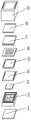
图1为一种Ku/Ka双频段TR组件SiP爆炸示意图;Figure 1 is a schematic diagram of SiP explosion of a Ku/Ka dual-band TR component;
图2为Ku频段TR组件原理框图;Figure 2 is a schematic block diagram of the Ku-band TR component;
图3为Ka频段TR组件原理框图。Figure 3 is a block diagram of the Ka-band TR components.
附图标记:1-Ku/Ka双频段SiP顶部金属盖板,2-Ku频段SiP壳体,3-Ku频段功放塑封器件,4-Ku频段SiP陶瓷盖板,5-Ka频段多功能移相衰减裸芯片,6-Ka频段控制器裸芯片,7-Ka频段控制器裸芯片陶瓷载板,8-Ka频段功放塑封器件,9-Ku/Ka双频段SiP壳体。Reference signs: 1-Ku/Ka dual-band SiP top metal cover, 2-Ku-band SiP housing, 3-Ku-band power amplifier plastic packaged device, 4-Ku-band SiP ceramic cover, 5-Ka-band multi-functional phase shifter Attenuation bare chip, 6-Ka frequency band controller bare chip, 7-Ka frequency band controller bare chip ceramic substrate, 8-Ka frequency band power amplifier plastic package device, 9-Ku/Ka dual-band SiP shell.
具体实施方式detailed description
需要说明的是,术语“第一”和“第二”等之类的关系术语仅仅用来将一个实体或者操作与另一个实体或操作区分开来,而不一定要求或者暗示这些实体或操作之间存在任何这种实际的关系或者顺序。而且,术语“包括”、“包含”或者其任何其他变体意在涵盖非排他性的包含,从而使得包括一系列要素的过程、方法、物品或者设备不仅包括那些要素,而且还包括没有明确列出的其他要素,或者是还包括为这种过程、方法、物品或者设备所固有的要素。在没有更多限制的情况下,由语句“包括一个……”限定的要素,并不排除在包括所述要素的过程、方法、物品或者设备中还存在另外的相同要素。It should be noted that relative terms such as the terms "first" and "second" are only used to distinguish one entity or operation from another entity or operation, and do not necessarily require or imply any relationship between these entities or operations. There is no such actual relationship or order between them. Furthermore, the term "comprises", "comprises" or any other variation thereof is intended to cover a non-exclusive inclusion such that a process, method, article, or apparatus comprising a set of elements includes not only those elements, but also includes elements not expressly listed. other elements of or also include elements inherent in such a process, method, article, or device. Without further limitations, an element defined by the phrase "comprising a ..." does not exclude the presence of additional identical elements in the process, method, article or apparatus comprising said element.
下面结合实施例对本发明的特征和性能作进一步的详细描述。The characteristics and performance of the present invention will be further described in detail below in conjunction with the examples.
实施例一Embodiment one
在卫星通信、雷达探测中,越来越多的工作于Ku和Ka频段,尤其是在雷达探测领域,为了获得更好的探测精度以及抗干扰性能,会使用多个频段的信号,由于Ka频段约等于Ku频段的2倍,这就使得Ku、Ka在多频段共口径相控阵雷达中得到广泛使用;但目前针对于Ku/Ka双频段共口径相控阵雷达中,双频段TR组件体积大、设计复杂、成本高。In satellite communication and radar detection, more and more people work in Ku and Ka frequency bands, especially in the field of radar detection. In order to obtain better detection accuracy and anti-interference performance, signals in multiple frequency bands will be used. Due to the Ka frequency band It is about twice that of the Ku frequency band, which makes Ku and Ka widely used in multi-band common-aperture phased array radars; but currently for Ku/Ka dual-band common-aperture phased array radars, the volume of dual-band TR components Large, complex design, high cost.
在本实施例中,针对于上述问题,提出了一种Ku/Ka双频段TR组件SiP设计方法,基于微系统技术,将1组Ku频段TR组件和4组Ka频段TR组件封装在一个SiP芯片中,实现Ku/Ka频段信号的收发以及波束控制等功能;具体采用高温共烧陶瓷作为基板,集成射频开关、功放、低噪放、多功能移相衰减裸芯片等,通过SiP垂直互联、三维堆叠封装技术实现包含1组Ku频段TR组件、4组Ka频段TR组件SiP芯片。In this embodiment, aiming at the above problems, a SiP design method for Ku/Ka dual-band TR components is proposed. Based on microsystem technology, 1 set of Ku-band TR components and 4 sets of Ka-band TR components are packaged in one SiP chip Among them, the Ku/Ka frequency band signal transmission and reception and beam control and other functions are realized; specifically, high-temperature co-fired ceramics are used as the substrate to integrate RF switches, power amplifiers, low-noise amplifiers, multi-functional phase-shifting attenuation bare chips, etc., through SiP vertical interconnection, three-dimensional Stacked packaging technology realizes SiP chips including 1 set of Ku-band TR components and 4 sets of Ka-band TR components.
需要说明的是,Ku频段TR组件原理框图如图2所示,Ka频段TR组件原理框图如图3所示。It should be noted that the functional block diagram of the TR component in the Ku-band is shown in FIG. 2 , and the functional block diagram of the TR component in the Ka-band is shown in FIG. 3 .
请参阅图1-3,一种Ku/Ka双频段TR组件SiP设计方法,具体包括如下步骤:Please refer to Figure 1-3, a SiP design method for Ku/Ka dual-band TR components, including the following steps:
步骤S1:根据设计要求完成Ku/Ka双频段SiP壳体、Ku频段SiP壳体、Ka频段控制器裸芯片陶瓷载板、Ku频段SiP陶瓷盖板、Ku/Ka双频段SiP顶部金属盖板订制;优选地,所述步骤S1,包括:Step S1: Complete the Ku/Ka dual-band SiP housing, Ku-band SiP housing, Ka-band controller bare chip ceramic substrate, Ku-band SiP ceramic cover, and Ku/Ka dual-band SiP top metal cover according to the design requirements. system; preferably, the step S1 includes:
根据设计要求完成Ku频段SiP金属围框和Ku/Ka双频段SiP金属围框的订制;Complete the customization of Ku-band SiP metal enclosures and Ku/Ka dual-band SiP metal enclosures according to design requirements;
根据设计要求完成Ku频段SiP的HTCC高温陶瓷壳体和Ku/Ka双频段SiP的HTCC高温陶瓷壳体;Complete the HTCC high-temperature ceramic shell of Ku-band SiP and the HTCC high-temperature ceramic shell of Ku/Ka dual-band SiP according to the design requirements;
将Ku/Ka双频段SiP的HTCC高温陶瓷壳体和Ku/Ka双频段SiP金属围框通过高温烧结成一体,形成Ku/Ka双频段SiP壳体;The Ku/Ka dual-band SiP HTCC high-temperature ceramic shell and the Ku/Ka dual-band SiP metal frame are sintered at high temperature to form a Ku/Ka dual-band SiP shell;
将Ku频段SiP的HTCC高温陶瓷壳体和Ku频段SiP金属围框通过高温烧结成一体,形成Ku频段SiP壳体。The HTCC high-temperature ceramic shell of the Ku-band SiP and the metal frame of the Ku-band SiP are sintered at high temperature to form a Ku-band SiP shell.
步骤S2:根据设计要求完成Ku频段功放塑封器件、Ka频段功放塑封器件订制;优选地,所述步骤S2将对应的裸芯片进行塑封,形成可进行SMT焊装的器件形式,便于装配、工艺操作及测试。Step S2: According to the design requirements, complete the customization of Ku-band power amplifier plastic-packaged devices and Ka-band power amplifier plastic-packaged devices; preferably, the step S2 plastic-packages the corresponding bare chips to form a device form that can be soldered by SMT, which is convenient for assembly and process Operation and testing.
步骤S3:将Ka频段射频开关、Ka频段低噪放裸芯片、Ka频段功放塑封器件装配到Ku/Ka双频段SiP壳体内;优选地,所述步骤S3,包括:Step S3: Assembling the Ka-band radio frequency switch, the Ka-band low-noise amplifier bare chip, and the Ka-band power amplifier plastic package into the Ku/Ka dual-band SiP housing; preferably, the step S3 includes:
在Ku/Ka双频段SiP的HTCC高温陶瓷壳体底部组装热沉,将Ka频段射频开关、Ka频段低噪放裸芯片采用高温导电胶工艺粘接在底部热沉上,并进行焊接;A heat sink is assembled at the bottom of the HTCC high-temperature ceramic shell of Ku/Ka dual-band SiP, and the Ka-band RF switch and the Ka-band low-noise amplifier bare chip are bonded to the bottom heat sink by high-temperature conductive adhesive technology and welded;
采用微组装工艺将Ka频段功放塑封器件装配到Ku/Ka双频段SiP的HTCC高温陶瓷上。The Ka-band power amplifier plastic-encapsulated device is assembled on the HTCC high-temperature ceramic of Ku/Ka dual-band SiP by using a micro-assembly process.
步骤S4:将Ka频段多功能移相衰减裸芯片和Ka频段控制器裸芯片装配到Ka频段控制器裸芯片陶瓷载板上,形成Ka频段模块;优选地,所述步骤S4,包括:Step S4: Assembling the Ka-band multifunctional phase-shifting attenuation bare chip and the Ka-band controller bare chip onto the Ka-band controller bare-chip ceramic substrate to form a Ka-band module; preferably, the step S4 includes:
将Ka频段多功能移相衰减裸芯片和Ka频段控制器裸芯片采用金丝键合工艺装配到Ka频段控制器裸芯片陶瓷载板上。The Ka-band multifunctional phase-shifting attenuation bare chip and the Ka-band controller bare chip are assembled on the Ka-band controller bare-chip ceramic carrier board by gold wire bonding.
步骤S5:将Ka频段模块装配到Ku/Ka双频段SiP壳体内;优选地,所述步骤S5,包括:Step S5: Assembling the Ka frequency-band module into the Ku/Ka dual-band SiP housing; preferably, the step S5 includes:
采用微组装工艺将Ka频段模块装配到Ku/Ka双频段SiP的HTCC高温陶瓷壳体上,并用并用红胶固定焊点。The Ka-band module is assembled on the HTCC high-temperature ceramic shell of the Ku/Ka dual-band SiP using a micro-assembly process, and the solder joints are fixed with red glue.
步骤S6:将Ku频段射频开关、Ku频段低噪放裸芯片、Ku频段功放塑封器件装配到Ku频段SiP壳体内;优选地,所述步骤S6,包括:Step S6: Assembling the Ku-band radio frequency switch, the Ku-band low-noise amplifier bare chip, and the Ku-band power amplifier plastic-encapsulated device into the Ku-band SiP housing; preferably, the step S6 includes:
在Ku频段SiP的HTCC高温陶瓷壳体底部组装热沉,将Ku频段低噪放裸芯片、Ku频段射频开关通过高温导电胶工艺粘接在底部热沉上,并进行焊接;A heat sink is assembled at the bottom of the HTCC high-temperature ceramic shell of the Ku-band SiP, and the Ku-band low-noise amplifier bare chip and the Ku-band RF switch are bonded to the bottom heat sink by high-temperature conductive adhesive technology and welded;
采用微组装工艺将Ku频段功放塑封器件装配到Ku频段SiP的HTCC高温陶瓷壳体上。The Ku-band power amplifier plastic-encapsulated device is assembled on the HTCC high-temperature ceramic shell of the Ku-band SiP by using a micro-assembly process.
步骤S7:将Ku频段SiP陶瓷盖板装配到Ku频段SiP壳体上,形成Ku频段模块;优选地,所述步骤S7,包括:Step S7: Assembling the Ku-band SiP ceramic cover plate onto the Ku-band SiP housing to form a Ku-band module; preferably, the step S7 includes:
采用微组装工艺将Ku频段SiP陶瓷盖板装配到Ku频段SiP的HTCC高温陶瓷壳体上,形成Ku频段模块。The Ku-band SiP ceramic cover plate is assembled to the HTCC high-temperature ceramic shell of the Ku-band SiP by using a micro-assembly process to form a Ku-band module.
步骤S8:将Ku频段模块装配到Ku/Ka双频段SiP壳体内;优选地,所述步骤S8,包括:Step S8: Assembling the Ku-band module into the Ku/Ka dual-band SiP housing; preferably, the step S8 includes:
采用微组装工艺将Ku频段模块装配到Ku/Ka双频段SiP的HTCC高温陶瓷壳体。The Ku-band module is assembled into the HTCC high-temperature ceramic housing of the Ku/Ka dual-band SiP using a micro-assembly process.
步骤S9:将Ku/Ka双频段SiP顶部金属盖板与Ku/Ka双频段SiP壳体进行焊接密封;优选地,所述步骤S9,包括:Step S9: welding and sealing the Ku/Ka dual-band SiP top metal cover plate and the Ku/Ka dual-band SiP housing; preferably, the step S9 includes:
采用平行封焊工艺将Ku/Ka双频段SiP顶部金属盖板与Ku/Ka双频段SiP的HTCC高温陶瓷壳体进行焊接密封。The Ku/Ka dual-band SiP top metal cover plate and the Ku/Ka dual-band SiP HTCC high-temperature ceramic shell are welded and sealed by parallel sealing and welding process.
以上所述实施例仅表达了本申请的具体实施方式,其描述较为具体和详细,但并不能因此而理解为对本申请保护范围的限制。应当指出的是,对于本领域的普通技术人员来说,在不脱离本申请技术方案构思的前提下,还可以做出若干变形和改进,这些都属于本申请的保护范围。The above-mentioned embodiments only express the specific implementation manners of the present application, and the descriptions thereof are relatively specific and detailed, but should not be construed as limiting the protection scope of the present application. It should be noted that those skilled in the art can make several modifications and improvements without departing from the concept of the technical solution of the present application, and these all belong to the protection scope of the present application.
提供本背景技术部分是为了大体上呈现本发明的上下文,当前所署名的发明人的工作、在本背景技术部分中所描述的程度上的工作以及本部分描述在申请时尚不构成现有技术的方面,既非明示地也非暗示地被承认是本发明的现有技术。This Background section is provided to generally present the context of the invention, the work of the presently named inventors, to the extent described in this Background section, and what this section describes did not constitute prior art at the time of filing. aspects, are neither expressly nor impliedly admitted to be prior art to the present invention.
Claims (10)
Priority Applications (1)
| Application Number | Priority Date | Filing Date | Title |
|---|---|---|---|
| CN202211051861.3ACN115469275A (en) | 2022-08-31 | 2022-08-31 | A SiP design method for Ku/Ka dual-band TR components |
Applications Claiming Priority (1)
| Application Number | Priority Date | Filing Date | Title |
|---|---|---|---|
| CN202211051861.3ACN115469275A (en) | 2022-08-31 | 2022-08-31 | A SiP design method for Ku/Ka dual-band TR components |
Publications (1)
| Publication Number | Publication Date |
|---|---|
| CN115469275Atrue CN115469275A (en) | 2022-12-13 |
Family
ID=84370915
Family Applications (1)
| Application Number | Title | Priority Date | Filing Date |
|---|---|---|---|
| CN202211051861.3APendingCN115469275A (en) | 2022-08-31 | 2022-08-31 | A SiP design method for Ku/Ka dual-band TR components |
Country Status (1)
| Country | Link |
|---|---|
| CN (1) | CN115469275A (en) |
Citations (6)
| Publication number | Priority date | Publication date | Assignee | Title |
|---|---|---|---|---|
| CN112635444A (en)* | 2020-12-22 | 2021-04-09 | 中国电子科技集团公司第五十五研究所 | Three-dimensional stacked microsystem packaging assembly and manufacturing method thereof |
| CN112652613A (en)* | 2020-12-22 | 2021-04-13 | 中国电子科技集团公司第五十五研究所 | Multi-channel micro-system packaging assembly with three-dimensional stacking form and manufacturing method thereof |
| CN113838845A (en)* | 2021-11-26 | 2021-12-24 | 成都雷电微力科技股份有限公司 | TR assembly based on three-dimensional stacked airtight package and assembling method |
| CN114242661A (en)* | 2021-09-28 | 2022-03-25 | 中国船舶重工集团公司第七二三研究所 | A low-warpage double-layer stacked ceramic system and packaging method |
| CN114613751A (en)* | 2022-03-01 | 2022-06-10 | 中国电子科技集团公司第十研究所 | High-power three-dimensional stacked three-dimensional integrated radio frequency front end micro-system |
| CN114852951A (en)* | 2022-03-18 | 2022-08-05 | 中国电子科技集团公司第十三研究所 | W-band multichannel transmitting and receiving system and preparation method |
- 2022
- 2022-08-31CNCN202211051861.3Apatent/CN115469275A/enactivePending
Patent Citations (6)
| Publication number | Priority date | Publication date | Assignee | Title |
|---|---|---|---|---|
| CN112635444A (en)* | 2020-12-22 | 2021-04-09 | 中国电子科技集团公司第五十五研究所 | Three-dimensional stacked microsystem packaging assembly and manufacturing method thereof |
| CN112652613A (en)* | 2020-12-22 | 2021-04-13 | 中国电子科技集团公司第五十五研究所 | Multi-channel micro-system packaging assembly with three-dimensional stacking form and manufacturing method thereof |
| CN114242661A (en)* | 2021-09-28 | 2022-03-25 | 中国船舶重工集团公司第七二三研究所 | A low-warpage double-layer stacked ceramic system and packaging method |
| CN113838845A (en)* | 2021-11-26 | 2021-12-24 | 成都雷电微力科技股份有限公司 | TR assembly based on three-dimensional stacked airtight package and assembling method |
| CN114613751A (en)* | 2022-03-01 | 2022-06-10 | 中国电子科技集团公司第十研究所 | High-power three-dimensional stacked three-dimensional integrated radio frequency front end micro-system |
| CN114852951A (en)* | 2022-03-18 | 2022-08-05 | 中国电子科技集团公司第十三研究所 | W-band multichannel transmitting and receiving system and preparation method |
Non-Patent Citations (3)
| Title |
|---|
| MING LIU: "Design and Implementation of a Compact Dual-band RF System-in-Package Module", 《ICMMT2020》, 31 December 2020 (2020-12-31), pages 1 - 3* |
| 刘晓政: "基于 CBGA 技术的双频段四通道变频SiP", 《雷达科学与技术》, vol. 20, no. 4, 30 April 2022 (2022-04-30), pages 202 - 206* |
| 张鸣一: "Ku/Ka波段双频T/R组件关键技术研究", 《中国优秀硕士学位论文全文数据库 信息科技辑》, vol. 2022, no. 3, 15 March 2022 (2022-03-15), pages 136 - 1778* |
Similar Documents
| Publication | Publication Date | Title |
|---|---|---|
| CN111048500B (en) | All-in-one packaged RF microsystem components | |
| US6995630B2 (en) | High-frequency compound switch module and communication terminal using it | |
| US5019829A (en) | Plug-in package for microwave integrated circuit having cover-mounted antenna | |
| CN105866747A (en) | Active phased array radar transmit-receive component and manufacturing method thereof | |
| CN205594153U (en) | Active phased array radar receives and dispatches subassembly | |
| EP2466638A2 (en) | High frequency module | |
| CN112005501B (en) | High-frequency module and communication device provided with same | |
| CN105281675B (en) | A kind of big instant bandwidth down conversion module of ultra wide band and its conversion method | |
| US20220278703A1 (en) | Radio frequency module and communication device | |
| CN105099484A (en) | Global frequency range RFFE module and system thereof | |
| US5376901A (en) | Hermetically sealed millimeter waveguide launch transition feedthrough | |
| US20060103003A1 (en) | Modular construction component with encapsulation | |
| JP2000031712A (en) | Microstrip line-waveguide conversion structure, high frequency signal integrated circuit package and its manufacture | |
| CN116073849A (en) | POP stacking integrated miniature broadband transceiving frequency conversion module and assembly method thereof | |
| CN111756334A (en) | A Stereo Micro-Assembled Low-Frequency Dual-Band Drive Power Amplifier | |
| KR20000029387A (en) | Module of components superimposed in one and the same package | |
| CN115469275A (en) | A SiP design method for Ku/Ka dual-band TR components | |
| US20190166694A1 (en) | Circuit module | |
| CN117393985B (en) | Airtight power synthesis device and implementation method | |
| CN104833960A (en) | T/R device | |
| CN112117238B (en) | Miniaturized optoelectronic oscillator based on SIP packaging technology | |
| CN205142138U (en) | Frequency conversion module under big instant bandwidth of ultra wide band | |
| CN115458517A (en) | A Ka-band TR module SiP chip structure and its design method | |
| Bechtold | Innovation steps towards a novel and cost efficient LTCC packaging technology for high end applications | |
| CN210536612U (en) | Three-dimensional stacking frequency source |
Legal Events
| Date | Code | Title | Description |
|---|---|---|---|
| PB01 | Publication | ||
| PB01 | Publication | ||
| SE01 | Entry into force of request for substantive examination | ||
| SE01 | Entry into force of request for substantive examination |