CN115459777A - Biasing circuit suitable for differential current steering DAC - Google Patents
Biasing circuit suitable for differential current steering DACDownload PDFInfo
- Publication number
- CN115459777A CN115459777ACN202211163528.1ACN202211163528ACN115459777ACN 115459777 ACN115459777 ACN 115459777ACN 202211163528 ACN202211163528 ACN 202211163528ACN 115459777 ACN115459777 ACN 115459777A
- Authority
- CN
- China
- Prior art keywords
- terminal
- nmos transistor
- gate
- drain
- transistor
- Prior art date
- Legal status (The legal status is an assumption and is not a legal conclusion. Google has not performed a legal analysis and makes no representation as to the accuracy of the status listed.)
- Pending
Links
Images
Classifications
- H—ELECTRICITY
- H03—ELECTRONIC CIRCUITRY
- H03M—CODING; DECODING; CODE CONVERSION IN GENERAL
- H03M1/00—Analogue/digital conversion; Digital/analogue conversion
- H03M1/66—Digital/analogue converters
- H03M1/74—Simultaneous conversion
- H03M1/742—Simultaneous conversion using current sources as quantisation value generators
- H03M1/745—Simultaneous conversion using current sources as quantisation value generators with weighted currents
Landscapes
- Engineering & Computer Science (AREA)
- Theoretical Computer Science (AREA)
- Amplifiers (AREA)
Abstract
Description
Translated fromChinese技术领域technical field
本发明涉及集成电路技术领域,特别涉及一种适用于差分电流舵DAC的偏置电路。The invention relates to the technical field of integrated circuits, in particular to a bias circuit suitable for a differential current steering DAC.
背景技术Background technique
DAC(数模转换器)是对数字电路和模拟电路之间的数据进行传输的纽带,主要作用是将数字输入量转换成模拟输出量。DAC在科技发展迅速的今天,已经成为不可缺少的重要功能模块,涉及通信技术、自动化控制技术和图像处理技术等多个领域。DAC (Digital-to-Analog Converter) is the link for data transmission between digital circuits and analog circuits, and its main function is to convert digital input into analog output. Today, with the rapid development of science and technology, DAC has become an indispensable and important functional module, involving many fields such as communication technology, automatic control technology and image processing technology.
在不同的应用场合中,对DAC的性能有着截然不同的要求。例如,视频和音频等领域的产品一般对DAC输出的线性度、尖峰毛刺、建立时间等时域特性要求较高;在通信领域中邻近信道的信号是否会对目标信道的信号产生干扰则更为关键,因此需要格外注重无杂散动态范围(Spurious Free Dynamic Range,SFDR)和带宽等频域特性的提升。近年来,为了适应数字信号处理系统的迅猛发展,高速高性能DAC的研究与设计已然成为一个重要趋势。In different applications, there are completely different requirements for the performance of the DAC. For example, products in the fields of video and audio generally have higher requirements on time-domain characteristics such as DAC output linearity, spikes, and settling time; in the field of communication, whether signals of adjacent channels will interfere with signals of the target channel is more important Therefore, it is necessary to pay special attention to the improvement of frequency domain characteristics such as spurious free dynamic range (Spurious Free Dynamic Range, SFDR) and bandwidth. In recent years, in order to adapt to the rapid development of digital signal processing systems, the research and design of high-speed and high-performance DAC has become an important trend.
电流舵DAC的转换过程是通过数字输入信号对一系列相互匹配的电流源开关进行控制来实现的,电流源阵列的匹配性影响DAC的线性度。对于二进制码电流舵型DAC电路,由于各个输入位权值的不同,电流源中存在器件失配以及时钟馈通,这些非理想效应容易产生较大的DNL以及动态误差,必须进行仔细的分析并及时做出处理。The conversion process of the current steering DAC is realized by controlling a series of matched current source switches through the digital input signal, and the matching of the current source array affects the linearity of the DAC. For the binary code current steering DAC circuit, due to the different weights of each input bit, there are device mismatches and clock feedthrough in the current source. These non-ideal effects are likely to cause large DNL and dynamic errors, which must be carefully analyzed and analyzed. Deal with it in a timely manner.
发明内容Contents of the invention
本发明的目的在于提供一种适用于差分电流舵DAC的偏置电路,以解决背景技术中的问题。The purpose of the present invention is to provide a bias circuit suitable for a differential current steering DAC, so as to solve the problems in the background technology.
为解决上述技术问题,本发明提供了一种适用于差分电流舵DAC的偏置电路,包括箝位电压产生模块和栅端偏置电压产生模块;In order to solve the above technical problems, the present invention provides a bias circuit suitable for a differential current steering DAC, including a clamp voltage generation module and a gate bias voltage generation module;
所述箝位电压产生模块通过运算跨导放大器OTA和电流镜网络产生箝位电压,作为跨阻放大器的输入,以箝位差分DAC开关电流源阵列输出端电压;The clamping voltage generation module generates the clamping voltage through the operational transconductance amplifier OTA and the current mirror network, as the input of the transimpedance amplifier, to clamp the differential DAC switching current source array output terminal voltage;
所述栅端偏置电压产生模块通过运算放大器OP和电流镜网络产生差分DAC中PMOS电流源阵列的栅端偏置电压和NMOS电流源阵列的栅端偏置电压。The gate bias voltage generation module generates the gate bias voltage of the PMOS current source array and the gate bias voltage of the NMOS current source array in the differential DAC through the operational amplifier OP and the current mirror network.
在一种实施方式中,所述箝位电压产生模块包括PMOS管MP3~MP4、NMOS管MN4~MN5和MN7~MN8、运算跨导放大器OTA、电阻R3~R6、电容C2;In one embodiment, the clamp voltage generation module includes PMOS transistors MP3-MP4, NMOS transistors MN4-MN5 and MN7-MN8, an operational transconductance amplifier OTA, resistors R3-R6, and a capacitor C2;
PMOS管MP3的源端和PMOS管MP4的源端均连接电源VDD,PMOS管MP3的栅端和PMOS管MP4的栅端连接,PMOS管MP3的漏端同时连接自身栅端和NMOS管MN4的漏端;PMOS管MP4的漏端依次通过电阻R3和电容C2接地;The source terminal of the PMOS transistor MP3 and the source terminal of the PMOS transistor MP4 are both connected to the power supply VDD, the gate terminal of the PMOS transistor MP3 is connected to the gate terminal of the PMOS transistor MP4, and the drain terminal of the PMOS transistor MP3 is connected to its own gate terminal and the drain of the NMOS transistor MN4 at the same time. end; the drain end of the PMOS transistor MP4 is grounded sequentially through the resistor R3 and the capacitor C2;
NMOS管MN8的漏端连接PMOS管MP4的漏端,栅端接电源VDD,源端接NMOS管MN7的漏端;NMOS管MN7的栅端接在电阻R3和电容C2之间,源端通过电阻R4连接运算跨导放大器OTA的输出端;NMOS管MN5的漏端连接NMOS管MN7的源端,栅端连接NMOS管MN4的栅端,源端接地;NMOS管MN4的源端接地;The drain terminal of the NMOS transistor MN8 is connected to the drain terminal of the PMOS transistor MP4, the gate terminal is connected to the power supply VDD, and the source terminal is connected to the drain terminal of the NMOS transistor MN7; the gate terminal of the NMOS transistor MN7 is connected between the resistor R3 and the capacitor C2, and the source terminal passes through the resistor R4 is connected to the output end of the operational transconductance amplifier OTA; the drain end of the NMOS transistor MN5 is connected to the source end of the NMOS transistor MN7, the gate end is connected to the gate end of the NMOS transistor MN4, and the source end is grounded; the source end of the NMOS transistor MN4 is grounded;
电阻R5的一端连接电源VDD,另一端通过电阻R6接地;运算跨导放大器OTA的正输入端连接在电阻R5和R6之间,负输入端连接自身的输出端形成反馈。One end of the resistor R5 is connected to the power supply VDD, and the other end is grounded through the resistor R6; the positive input terminal of the operational transconductance amplifier OTA is connected between the resistors R5 and R6, and the negative input terminal is connected to its own output terminal to form feedback.
在一种实施方式中,所述栅端偏置电压产生模块包括PMOS管MP1~MP2和MP5、NMOS管MN2~MN3和MN6、电阻R1~R2、电容C1和运算放大器OP;In one embodiment, the gate bias voltage generating module includes PMOS transistors MP1-MP2 and MP5, NMOS transistors MN2-MN3 and MN6, resistors R1-R2, capacitor C1 and an operational amplifier OP;
PMOS管MP1的源端和PMOS管MP2的源端均接电源VDD,PMOS管MP1的栅端连接PMOS管MP2的栅端,PMOS管MP1的漏端通过电阻R1连接NMOS管MN2的漏端;PMOS管MP2的栅端连接PMOS管MP1的漏端,PMOS管MP2的漏端连接PMOS管MP5的源端;The source end of the PMOS transistor MP1 and the source end of the PMOS transistor MP2 are both connected to the power supply VDD, the gate end of the PMOS transistor MP1 is connected to the gate end of the PMOS transistor MP2, and the drain end of the PMOS transistor MP1 is connected to the drain end of the NMOS transistor MN2 through a resistor R1; The gate end of the transistor MP2 is connected to the drain end of the PMOS transistor MP1, and the drain end of the PMOS transistor MP2 is connected to the source end of the PMOS transistor MP5;
PMOS管MP5的栅端接地,漏端连接NMOS管MN6的漏端;NMOS管MN6的栅端连接电源VDD,源端连接NMOS管MN3的漏端;NMOS管MN3的栅端连接运算放大器OP的输出端,源端接地;NMOS管MN2的栅端同时连接NMOS管MN4的栅端、NMOS管MN5的栅端,源端接地;The gate terminal of the PMOS transistor MP5 is grounded, and the drain terminal is connected to the drain terminal of the NMOS transistor MN6; the gate terminal of the NMOS transistor MN6 is connected to the power supply VDD, and the source terminal is connected to the drain terminal of the NMOS transistor MN3; the gate terminal of the NMOS transistor MN3 is connected to the output of the operational amplifier OP terminal, the source terminal is grounded; the gate terminal of the NMOS transistor MN2 is connected to the gate terminal of the NMOS transistor MN4 and the gate terminal of the NMOS transistor MN5 at the same time, and the source terminal is grounded;
电阻R2的第一端同时连接PMOS管MP5的漏端、NMOS管MN6的漏端和运算放大器OP的正输入端,第二端通过电容C1连接运算放大器OP的输出端。The first terminal of the resistor R2 is simultaneously connected to the drain terminal of the PMOS transistor MP5, the drain terminal of the NMOS transistor MN6 and the positive input terminal of the operational amplifier OP, and the second terminal is connected to the output terminal of the operational amplifier OP through the capacitor C1.
在一种实施方式中,所述适用于差分电流舵DAC的偏置电路还包括NMOS管MN1,NMOS管MN1的漏端同时连接自身栅端、NMOS管MN2的栅端、NMOS管MN4的栅端和NMOS管MN5的栅端,NMOS管MN1的源端接地。In one embodiment, the bias circuit applicable to a differential current steering DAC further includes an NMOS transistor MN1, and the drain terminal of the NMOS transistor MN1 is simultaneously connected to its own gate terminal, the gate terminal of the NMOS transistor MN2, and the gate terminal of the NMOS transistor MN4. and the gate terminal of the NMOS transistor MN5, and the source terminal of the NMOS transistor MN1 is grounded.
在本发明提供的一种适用于差分电流舵DAC的偏置电路中,包括箝位电压产生模块和栅端偏置电压产生模块。所述箝位电压产生模块通过运算跨导放大器OTA和电流镜网络产生箝位电压,作为跨阻放大器的输入,用于箝位差分DAC开关电流源阵列输出端电压,保证不同数字信号输入时,电流源阵列电流镜像管的漏端电压保持不变,提高DAC电流源阵列与参考电流源的匹配性;所述栅端偏置电压产生模块通过运算放大器OP和电流镜网络,产生差分DAC中PMOS电流源阵列的栅端偏置电压和NMOS电流源阵列的栅端偏置电压。A bias circuit suitable for a differential current steering DAC provided by the present invention includes a clamp voltage generation module and a gate bias voltage generation module. The clamping voltage generation module generates the clamping voltage through the operational transconductance amplifier OTA and the current mirror network, as the input of the transimpedance amplifier, and is used for clamping the voltage at the output terminal of the differential DAC switching current source array to ensure that when different digital signals are input, The drain terminal voltage of the current source array current mirror tube remains unchanged, which improves the matching between the DAC current source array and the reference current source; the gate bias voltage generation module generates the PMOS in the differential DAC through the operational amplifier OP and the current mirror network. The gate terminal bias voltage of the current source array and the gate terminal bias voltage of the NMOS current source array.
附图说明Description of drawings
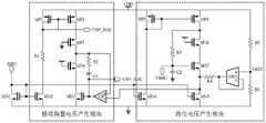
图1是本发明提供的一种适用于差分电流舵DAC的偏置电路结构示意图。FIG. 1 is a schematic structural diagram of a bias circuit suitable for a differential current steering DAC provided by the present invention.
具体实施方式detailed description
以下结合附图和具体实施例对本发明提出的一种适用于差分电流舵DAC的偏置电路作进一步详细说明。根据下面说明,本发明的优点和特征将更清楚。需说明的是,附图均采用非常简化的形式且均使用非精准的比例,仅用以方便、明晰地辅助说明本发明实施例的目的。A bias circuit suitable for a differential current steering DAC proposed by the present invention will be further described in detail below with reference to the accompanying drawings and specific embodiments. The advantages and features of the present invention will become clearer from the following description. It should be noted that all the drawings are in a very simplified form and use imprecise scales, and are only used to facilitate and clearly assist the purpose of illustrating the embodiments of the present invention.
本发明提供一种应用于差分DAC的偏置电路,其结构如图1所示,包括箝位电压产生模块和栅端偏置电压产生模块两个部分。The present invention provides a bias circuit applied to a differential DAC, the structure of which is shown in FIG. 1 , including two parts: a clamp voltage generation module and a gate bias voltage generation module.
所述箝位电压产生模块包括PMOS管MP3~MP4、NMOS管MN4~MN5和MN7~MN8、运算跨导放大器OTA、电阻R3~R6、电容C2。PMOS管MP3的源端和PMOS管MP4的源端均连接电源VDD,PMOS管MP3的栅端和PMOS管MP4的栅端连接,PMOS管MP3的漏端同时连接自身栅端和NMOS管MN4的漏端;PMOS管MP4的漏端依次通过电阻R3和电容C2接地;NMOS管MN8的漏端连接PMOS管MP4的漏端,栅端接电源VDD,源端接NMOS管MN7的漏端;NMOS管MN7的栅端接在电阻R3和电容C2之间,源端通过电阻R4连接运算跨导放大器OTA的输出端;NMOS管MN5的漏端连接NMOS管MN7的源端,栅端连接NMOS管MN4的栅端,源端接地;NMOS管MN4的源端接地;电阻R5的一端连接电源VDD,另一端通过电阻R6接地;运算跨导放大器OTA的正输入端连接在电阻R5和R6之间,负输入端连接自身的输出端形成反馈。所述适用于差分电流舵DAC的偏置电路还包括NMOS管MN1,NMOS管MN1的漏端同时连接自身栅端、NMOS管MN4的栅端和NMOS管MN5的栅端,NMOS管MN1的源端接地。The clamp voltage generating module includes PMOS transistors MP3-MP4, NMOS transistors MN4-MN5 and MN7-MN8, an operational transconductance amplifier OTA, resistors R3-R6, and a capacitor C2. The source terminal of the PMOS transistor MP3 and the source terminal of the PMOS transistor MP4 are both connected to the power supply VDD, the gate terminal of the PMOS transistor MP3 is connected to the gate terminal of the PMOS transistor MP4, and the drain terminal of the PMOS transistor MP3 is connected to its own gate terminal and the drain of the NMOS transistor MN4 at the same time. The drain end of the PMOS transistor MP4 is grounded sequentially through the resistor R3 and the capacitor C2; the drain end of the NMOS transistor MN8 is connected to the drain end of the PMOS transistor MP4, the gate end is connected to the power supply VDD, and the source end is connected to the drain end of the NMOS transistor MN7; the NMOS transistor MN7 The gate terminal of the NMOS transistor MN5 is connected to the source terminal of the NMOS transistor MN7, and the gate terminal is connected to the gate terminal of the NMOS transistor MN4 through the resistor R4. terminal, the source terminal is grounded; the source terminal of the NMOS tube MN4 is grounded; one end of the resistor R5 is connected to the power supply VDD, and the other end is grounded through the resistor R6; the positive input terminal of the operational transconductance amplifier OTA is connected between the resistors R5 and R6, and the negative input terminal Connect to its own output to form feedback. The bias circuit applicable to the differential current steering DAC also includes an NMOS transistor MN1, the drain terminal of the NMOS transistor MN1 is simultaneously connected to its own gate terminal, the gate terminal of the NMOS transistor MN4 and the gate terminal of the NMOS transistor MN5, and the source terminal of the NMOS transistor MN1 grounded.
MOS管MN1、MN4、MN5、MP3、MP4组成电流镜网络。通过控制电源电压VDD经过电阻R5和R6的分压值,电阻R4的阻值,MOS管MN4、MN5、MP3、MP4的镜像比例,保证MOS管MN5、MN7、MP4处于饱和区。MOS tubes MN1, MN4, MN5, MP3, MP4 form a current mirror network. By controlling the voltage division value of the power supply voltage VDD through the resistors R5 and R6, the resistance value of the resistor R4, and the mirror ratio of the MOS transistors MN4, MN5, MP3, and MP4, it is ensured that the MOS transistors MN5, MN7, and MP4 are in the saturation region.
所述箝位电压产生模块通过运算跨导放大器OTA的箝位功能,控制运算跨导放大器OTA输出端电压等于电源电压VDD经过电阻R5和R6的分压VREF。晶体管MN1、MN4、MN5、MP3和MP4并联MOS管个数分别为N1、N4、N5、P3和P4(N1>0、N4>0、N5>0、P3>0、P4>0)。根据MOS管电流镜像原则,流过NMOS管MN1的电流IBIN镜像到NMOS管MN5的镜像电流为


所述栅端偏置电压产生模块包括PMOS管MP1~MP2和MP5、NMOS管MN2~MN3和MN6、电阻R1~R2、电容C1和运算放大器OP。PMOS管MP1的源端和PMOS管MP2的源端均接电源VDD,PMOS管MP1的栅端连接PMOS管MP2的栅端,PMOS管MP1的漏端通过电阻R1连接NMOS管MN2的漏端;PMOS管MP2的栅端连接PMOS管MP1的漏端,PMOS管MP2的漏端连接PMOS管MP5的源端;PMOS管MP5的栅端接地,漏端连接NMOS管MN6的漏端;NMOS管MN6的栅端连接电源VDD,源端连接NMOS管MN3的漏端;NMOS管MN3的栅端连接运算放大器OP的输出端,源端接地;NMOS管MN2的栅端同时连接NMOS管MN4的栅端、NMOS管MN5的栅端,源端接地;电阻R2的第一端同时连接PMOS管MP5的漏端、NMOS管MN6的漏端和运算放大器OP的正输入端,第二端通过电容C1连接运算放大器OP的输出端。NMOS管MN1的漏端同时连接自身栅端和NMOS管MN2的栅端。The gate bias voltage generation module includes PMOS transistors MP1-MP2 and MP5, NMOS transistors MN2-MN3 and MN6, resistors R1-R2, capacitor C1 and operational amplifier OP. The source end of the PMOS transistor MP1 and the source end of the PMOS transistor MP2 are both connected to the power supply VDD, the gate end of the PMOS transistor MP1 is connected to the gate end of the PMOS transistor MP2, and the drain end of the PMOS transistor MP1 is connected to the drain end of the NMOS transistor MN2 through a resistor R1; The gate end of the tube MP2 is connected to the drain end of the PMOS transistor MP1, and the drain end of the PMOS transistor MP2 is connected to the source end of the PMOS transistor MP5; the gate end of the PMOS transistor MP5 is connected to the ground, and the drain end is connected to the drain end of the NMOS transistor MN6; the gate end of the NMOS transistor MN6 The source terminal is connected to the power supply VDD, the source terminal is connected to the drain terminal of the NMOS transistor MN3; the gate terminal of the NMOS transistor MN3 is connected to the output terminal of the operational amplifier OP, and the source terminal is grounded; the gate terminal of the NMOS transistor MN2 is simultaneously connected to the gate terminal of the NMOS transistor MN4, the NMOS transistor The gate terminal and source terminal of MN5 are grounded; the first terminal of resistor R2 is connected to the drain terminal of PMOS transistor MP5, the drain terminal of NMOS transistor MN6 and the positive input terminal of operational amplifier OP at the same time, and the second terminal is connected to the positive input terminal of operational amplifier OP through capacitor C1 output. The drain terminal of the NMOS transistor MN1 is connected to its own gate terminal and the gate terminal of the NMOS transistor MN2 at the same time.
MOS管MN1、MN2、MN3、MP1、MP2组成电流镜网络。通过控制电压VREF的大小,保证MOS管MN3、MP2处于饱和区。MOS transistors MN1, MN2, MN3, MP1, MP2 form a current mirror network. By controlling the magnitude of the voltage VREF, it is ensured that the MOS transistors MN3 and MP2 are in the saturation region.
所述栅端偏置电压产生模块通过运算放大器OP的箝位功能,控制NMOS管MN6的漏端电压等于NMOS管MN5的漏端电压。晶体管MN1、MN2、MP1和MP2并联MOS管个数分别为N1、N2、P1和P2(N1>0、N2>0、P1>0、P2>0)。根据MOS管电流镜像原则,流过NMOS管MN1的电流IBIN镜像到NMOS管MN2的镜像电流为


上述描述仅是对本发明较佳实施例的描述,并非对本发明范围的任何限定,本发明领域的普通技术人员根据上述揭示内容做的任何变更、修饰,均属于权利要求书的保护范围。The above description is only a description of the preferred embodiments of the present invention, and does not limit the scope of the present invention. Any changes and modifications made by those of ordinary skill in the field of the present invention based on the above disclosures shall fall within the protection scope of the claims.
Claims (4)
Translated fromChinesePriority Applications (1)
| Application Number | Priority Date | Filing Date | Title |
|---|---|---|---|
| CN202211163528.1ACN115459777A (en) | 2022-09-23 | 2022-09-23 | Biasing circuit suitable for differential current steering DAC |
Applications Claiming Priority (1)
| Application Number | Priority Date | Filing Date | Title |
|---|---|---|---|
| CN202211163528.1ACN115459777A (en) | 2022-09-23 | 2022-09-23 | Biasing circuit suitable for differential current steering DAC |
Publications (1)
| Publication Number | Publication Date |
|---|---|
| CN115459777Atrue CN115459777A (en) | 2022-12-09 |
Family
ID=84306523
Family Applications (1)
| Application Number | Title | Priority Date | Filing Date |
|---|---|---|---|
| CN202211163528.1APendingCN115459777A (en) | 2022-09-23 | 2022-09-23 | Biasing circuit suitable for differential current steering DAC |
Country Status (1)
| Country | Link |
|---|---|
| CN (1) | CN115459777A (en) |
Cited By (1)
| Publication number | Priority date | Publication date | Assignee | Title |
|---|---|---|---|---|
| CN117097318A (en)* | 2023-10-20 | 2023-11-21 | 中国电子科技集团公司第五十八研究所 | High-speed current rudder DAC self-adaptive switch amplitude limiting circuit |
Citations (6)
| Publication number | Priority date | Publication date | Assignee | Title |
|---|---|---|---|---|
| WO2001084705A1 (en)* | 2000-04-26 | 2001-11-08 | Maxim Integrated Products, Inc. | System and method for optimal biasing of a telescopic cascode operational transconductance amplifier (ota) |
| WO2003087855A1 (en)* | 2002-04-17 | 2003-10-23 | Danfoss Drives A/S | Method for measuring currents in a motor controller and motor controller using such method |
| US6801080B1 (en)* | 2003-04-07 | 2004-10-05 | Pericom Semiconductor Corp. | CMOS differential input buffer with source-follower input clamps |
| US20090289717A1 (en)* | 2008-05-20 | 2009-11-26 | Renesas Technology Corp. | Radio frequency (rf) power amplifier and rf power amplifier apparatus |
| CN107257947A (en)* | 2015-02-23 | 2017-10-17 | 高通股份有限公司 | Launch digital analog converter(DAC)Spuious decay |
| CN113271068A (en)* | 2021-04-02 | 2021-08-17 | 西安电子科技大学 | Low-noise amplifier with low power consumption for dual-power voltage transconductance calibration |
- 2022
- 2022-09-23CNCN202211163528.1Apatent/CN115459777A/enactivePending
Patent Citations (6)
| Publication number | Priority date | Publication date | Assignee | Title |
|---|---|---|---|---|
| WO2001084705A1 (en)* | 2000-04-26 | 2001-11-08 | Maxim Integrated Products, Inc. | System and method for optimal biasing of a telescopic cascode operational transconductance amplifier (ota) |
| WO2003087855A1 (en)* | 2002-04-17 | 2003-10-23 | Danfoss Drives A/S | Method for measuring currents in a motor controller and motor controller using such method |
| US6801080B1 (en)* | 2003-04-07 | 2004-10-05 | Pericom Semiconductor Corp. | CMOS differential input buffer with source-follower input clamps |
| US20090289717A1 (en)* | 2008-05-20 | 2009-11-26 | Renesas Technology Corp. | Radio frequency (rf) power amplifier and rf power amplifier apparatus |
| CN107257947A (en)* | 2015-02-23 | 2017-10-17 | 高通股份有限公司 | Launch digital analog converter(DAC)Spuious decay |
| CN113271068A (en)* | 2021-04-02 | 2021-08-17 | 西安电子科技大学 | Low-noise amplifier with low power consumption for dual-power voltage transconductance calibration |
Cited By (2)
| Publication number | Priority date | Publication date | Assignee | Title |
|---|---|---|---|---|
| CN117097318A (en)* | 2023-10-20 | 2023-11-21 | 中国电子科技集团公司第五十八研究所 | High-speed current rudder DAC self-adaptive switch amplitude limiting circuit |
| CN117097318B (en)* | 2023-10-20 | 2024-02-13 | 中国电子科技集团公司第五十八研究所 | A high-speed current steering DAC adaptive switching limiting circuit |
Similar Documents
| Publication | Publication Date | Title |
|---|---|---|
| CN108958345B (en) | Differential reference voltage buffer | |
| Hammerschmied et al. | Design and implementation of an untrimmed MOSFET-only 10-bit A/D converter with-79-dB THD | |
| CN101692603B (en) | Gain bootstrap type C class reverser and application circuit thereof | |
| CN202548685U (en) | Reference voltage buffer circuit | |
| US20100283527A1 (en) | Analog Switch | |
| CN109546981B (en) | Differential input circuit, amplifying circuit, and display device | |
| CN111817719B (en) | Reference level buffer suitable for pipelined ADC and pipelined ADC | |
| CN116795167B (en) | Current mirror structure circuit and method for realizing low-voltage input work | |
| CN110380699A (en) | Input buffer, differential input buffer and integrated circuit | |
| US7777655B2 (en) | Wideband switched current source | |
| Zhang et al. | An input buffer for 4 GS/s 14-b time-interleaved ADC | |
| CN107425845B (en) | Superposition operation circuit and floating voltage digital-to-analog conversion circuit | |
| CN115459777A (en) | Biasing circuit suitable for differential current steering DAC | |
| CN110460338B (en) | A sample and hold circuit | |
| CN119002614A (en) | Source follower and electronic device | |
| Elkafrawy et al. | Design and validation of a 10-bit current mode SAR ADC with 58.4 dB SFDR at 50 MS/s in 90 nm CMOS | |
| CN110350876A (en) | Preamplifier, difference preamplifier and integrated circuit | |
| CN115842550A (en) | Current steering digital-to-analog converter and high-frequency linearity improving method thereof | |
| CN116131858A (en) | Current rudder digital-to-analog conversion circuit, chip and electronic equipment | |
| CN112953420A (en) | Dynamic operational amplifier circuit with input tube in linear region | |
| Kumar et al. | A 12‐bit SC3 partially segmented current steering DAC with improved SFDR and bandwidth | |
| CN101958715B (en) | Audio digital-to-analog converter | |
| CN100539418C (en) | A kind of contactor that is used for semi digital filtering | |
| CN117517753B (en) | Current sampling circuit adopting resistance sampling and compatible with P, N type power tube | |
| CN115276575B (en) | An operational amplifier |
Legal Events
| Date | Code | Title | Description |
|---|---|---|---|
| PB01 | Publication | ||
| PB01 | Publication | ||
| SE01 | Entry into force of request for substantive examination | ||
| SE01 | Entry into force of request for substantive examination |