CN115394641A - Nitrogen-containing compounds for etching semiconductor structures - Google Patents
Nitrogen-containing compounds for etching semiconductor structuresDownload PDFInfo
- Publication number
- CN115394641A CN115394641ACN202211081337.0ACN202211081337ACN115394641ACN 115394641 ACN115394641 ACN 115394641ACN 202211081337 ACN202211081337 ACN 202211081337ACN 115394641 ACN115394641 ACN 115394641A
- Authority
- CN
- China
- Prior art keywords
- etch
- etching
- silicon
- layer
- nitrogen
- Prior art date
- Legal status (The legal status is an assumption and is not a legal conclusion. Google has not performed a legal analysis and makes no representation as to the accuracy of the status listed.)
- Pending
Links
- 238000005530etchingMethods0.000titleclaimsabstractdescription142
- QJGQUHMNIGDVPM-UHFFFAOYSA-Nnitrogen groupChemical group[N]QJGQUHMNIGDVPM-UHFFFAOYSA-N0.000titleclaimsabstractdescription95
- 239000004065semiconductorSubstances0.000titledescription12
- 239000000758substrateSubstances0.000claimsabstractdescription78
- 238000000034methodMethods0.000claimsabstractdescription73
- 229910052757nitrogenInorganic materials0.000claimsabstractdescription71
- 238000006243chemical reactionMethods0.000claimsabstractdescription66
- 229910052799carbonInorganic materials0.000claimsabstractdescription52
- 239000011261inert gasSubstances0.000claimsabstractdescription28
- KRHYYFGTRYWZRS-UHFFFAOYSA-NFluoraneChemical compoundFKRHYYFGTRYWZRS-UHFFFAOYSA-N0.000claimsabstractdescription24
- 125000000524functional groupChemical group0.000claimsabstractdescription19
- 230000003213activating effectEffects0.000claimsabstractdescription6
- 239000010410layerSubstances0.000claimsdescription210
- 238000000151depositionMethods0.000claimsdescription34
- 150000004812organic fluorine compoundsChemical class0.000claimsdescription32
- 229920000642polymerPolymers0.000claimsdescription29
- 239000012634fragmentSubstances0.000claimsdescription13
- CFPAMJZAMYOJER-UHFFFAOYSA-N2,3,3,3-tetrafluoropropanenitrileChemical compoundN#CC(F)C(F)(F)FCFPAMJZAMYOJER-UHFFFAOYSA-N0.000claimsdescription11
- DQFXLCKTFSDWHB-UHFFFAOYSA-N2,2-difluoroacetonitrileChemical compoundFC(F)C#NDQFXLCKTFSDWHB-UHFFFAOYSA-N0.000claimsdescription10
- 229910052786argonInorganic materials0.000claimsdescription10
- 238000002161passivationMethods0.000claimsdescription9
- NBVXSUQYWXRMNV-UHFFFAOYSA-NfluoromethaneChemical compoundFCNBVXSUQYWXRMNV-UHFFFAOYSA-N0.000claimsdescription7
- 229910052734heliumInorganic materials0.000claimsdescription7
- 150000002500ionsChemical class0.000claimsdescription7
- PIORIRQBACOORT-UHFFFAOYSA-N2,2,3,3-tetrafluoropropanenitrileChemical compoundFC(F)C(F)(F)C#NPIORIRQBACOORT-UHFFFAOYSA-N0.000claimsdescription6
- LHWSEFCIRYVTLZ-OWOJBTEDSA-N(e)-4,4,4-trifluorobut-2-enenitrileChemical compoundFC(F)(F)\C=C\C#NLHWSEFCIRYVTLZ-OWOJBTEDSA-N0.000claimsdescription5
- PFXBZIOMDHRUQQ-UHFFFAOYSA-N2-(1,1,1,3,3,3-hexafluoropropan-2-ylidene)propanedinitrileChemical groupFC(F)(F)C(C(F)(F)F)=C(C#N)C#NPFXBZIOMDHRUQQ-UHFFFAOYSA-N0.000claimsdescription5
- GNFVFPBRMLIKIM-UHFFFAOYSA-N2-fluoroacetonitrileChemical compoundFCC#NGNFVFPBRMLIKIM-UHFFFAOYSA-N0.000claimsdescription5
- WDGHUZCUXKJUJQ-UHFFFAOYSA-N3,3,3-trifluoropropanenitrileChemical compoundFC(F)(F)CC#NWDGHUZCUXKJUJQ-UHFFFAOYSA-N0.000claimsdescription5
- 229910052724xenonInorganic materials0.000claimsdescription5
- 229910052743kryptonInorganic materials0.000claimsdescription4
- 229910052754neonInorganic materials0.000claimsdescription4
- PZIVXXORSILYOQ-UHFFFAOYSA-N2,2,3,3,4,4,5,5-octafluorohexanedinitrileChemical compoundN#CC(F)(F)C(F)(F)C(F)(F)C(F)(F)C#NPZIVXXORSILYOQ-UHFFFAOYSA-N0.000claimsdescription3
- 239000011241protective layerSubstances0.000claimsdescription2
- SFFUEHODRAXXIA-UHFFFAOYSA-N2,2,2-trifluoroacetonitrileChemical compoundFC(F)(F)C#NSFFUEHODRAXXIA-UHFFFAOYSA-N0.000claims3
- FVBKAFXHWXBINM-UHFFFAOYSA-N2,2,3,3,4,4,5,5,5-nonafluoropentanenitrileChemical compoundFC(F)(F)C(F)(F)C(F)(F)C(F)(F)C#NFVBKAFXHWXBINM-UHFFFAOYSA-N0.000claims2
- KADDQZUTOFNHMA-UHFFFAOYSA-N2,2,3,4,4-pentafluorobut-3-enenitrileChemical compoundFC(F)=C(F)C(F)(F)C#NKADDQZUTOFNHMA-UHFFFAOYSA-N0.000claims2
- 150000001875compoundsChemical class0.000abstractdescription96
- 229910052710siliconInorganic materials0.000abstractdescription91
- 239000010703siliconSubstances0.000abstractdescription78
- XUIMIQQOPSSXEZ-UHFFFAOYSA-NSiliconChemical compound[Si]XUIMIQQOPSSXEZ-UHFFFAOYSA-N0.000abstractdescription77
- LIVNPJMFVYWSIS-UHFFFAOYSA-Nsilicon monoxideChemical compound[Si-]#[O+]LIVNPJMFVYWSIS-UHFFFAOYSA-N0.000description138
- 239000007789gasSubstances0.000description107
- VYPSYNLAJGMNEJ-UHFFFAOYSA-NSilicium dioxideChemical compoundO=[Si]=OVYPSYNLAJGMNEJ-UHFFFAOYSA-N0.000description62
- 229910052814silicon oxideInorganic materials0.000description59
- 229910052760oxygenInorganic materials0.000description53
- 239000001301oxygenSubstances0.000description52
- QVGXLLKOCUKJST-UHFFFAOYSA-Natomic oxygenChemical compound[O]QVGXLLKOCUKJST-UHFFFAOYSA-N0.000description51
- 239000000463materialSubstances0.000description48
- 210000002381plasmaAnatomy0.000description48
- 229910052581Si3N4Inorganic materials0.000description38
- HQVNEWCFYHHQES-UHFFFAOYSA-Nsilicon nitrideChemical compoundN12[Si]34N5[Si]62N3[Si]51N64HQVNEWCFYHHQES-UHFFFAOYSA-N0.000description38
- 239000000203mixtureSubstances0.000description33
- 230000008021depositionEffects0.000description31
- 230000008569processEffects0.000description31
- IJGRMHOSHXDMSA-UHFFFAOYSA-NAtomic nitrogenChemical compoundN#NIJGRMHOSHXDMSA-UHFFFAOYSA-N0.000description20
- 229920002120photoresistant polymerPolymers0.000description20
- 230000000052comparative effectEffects0.000description18
- 238000012360testing methodMethods0.000description18
- 235000012431wafersNutrition0.000description18
- QGZKDVFQNNGYKY-UHFFFAOYSA-NAmmoniaChemical compoundNQGZKDVFQNNGYKY-UHFFFAOYSA-N0.000description16
- 239000007800oxidant agentSubstances0.000description16
- -1oxygen radicalsChemical class0.000description15
- 238000001020plasma etchingMethods0.000description14
- 229910021419crystalline siliconInorganic materials0.000description10
- 229910021420polycrystalline siliconInorganic materials0.000description9
- 230000001965increasing effectEffects0.000description8
- 230000000873masking effectEffects0.000description8
- TXEYQDLBPFQVAA-UHFFFAOYSA-NtetrafluoromethaneChemical compoundFC(F)(F)FTXEYQDLBPFQVAA-UHFFFAOYSA-N0.000description8
- 230000008016vaporizationEffects0.000description8
- 238000004833X-ray photoelectron spectroscopyMethods0.000description7
- 230000000694effectsEffects0.000description7
- 239000012535impuritySubstances0.000description7
- 229910052751metalInorganic materials0.000description7
- 239000002184metalSubstances0.000description7
- 229920005591polysiliconPolymers0.000description7
- XKRFYHLGVUSROY-UHFFFAOYSA-NArgonChemical compound[Ar]XKRFYHLGVUSROY-UHFFFAOYSA-N0.000description6
- 239000011248coating agentSubstances0.000description6
- 238000000576coating methodMethods0.000description6
- 239000003989dielectric materialSubstances0.000description6
- 229910052731fluorineInorganic materials0.000description6
- 230000006870functionEffects0.000description6
- 239000007788liquidSubstances0.000description6
- 229910000069nitrogen hydrideInorganic materials0.000description6
- 238000009835boilingMethods0.000description5
- 239000012159carrier gasSubstances0.000description5
- 238000004519manufacturing processMethods0.000description5
- 230000015654memoryEffects0.000description5
- 239000002245particleSubstances0.000description5
- 150000003254radicalsChemical class0.000description5
- 229910010271silicon carbideInorganic materials0.000description5
- 229910003481amorphous carbonInorganic materials0.000description4
- 239000006117anti-reflective coatingSubstances0.000description4
- 230000005587bubblingEffects0.000description4
- 239000006227byproductSubstances0.000description4
- 239000003990capacitorSubstances0.000description4
- 230000003247decreasing effectEffects0.000description4
- 230000009977dual effectEffects0.000description4
- 230000000670limiting effectEffects0.000description4
- 238000005259measurementMethods0.000description4
- 150000004767nitridesChemical class0.000description4
- 230000036961partial effectEffects0.000description4
- HBMJWWWQQXIZIP-UHFFFAOYSA-Nsilicon carbideChemical compound[Si+]#[C-]HBMJWWWQQXIZIP-UHFFFAOYSA-N0.000description4
- 238000009834vaporizationMethods0.000description4
- 238000001039wet etchingMethods0.000description4
- VVRCKMPEMSAMST-UHFFFAOYSA-N1,1,1,3,3,3-hexafluoropropan-2-imineChemical compoundFC(F)(F)C(=N)C(F)(F)FVVRCKMPEMSAMST-UHFFFAOYSA-N0.000description3
- OKTJSMMVPCPJKN-UHFFFAOYSA-NCarbonChemical compound[C]OKTJSMMVPCPJKN-UHFFFAOYSA-N0.000description3
- KIGSGUMPYBUZFB-UHFFFAOYSA-NN,1,1,1,3,3,3-heptafluoropropan-2-amineChemical compoundFNC(C(F)(F)F)C(F)(F)FKIGSGUMPYBUZFB-UHFFFAOYSA-N0.000description3
- BOTDANWDWHJENH-UHFFFAOYSA-NTetraethyl orthosilicateChemical compoundCCO[Si](OCC)(OCC)OCCBOTDANWDWHJENH-UHFFFAOYSA-N0.000description3
- NRTOMJZYCJJWKI-UHFFFAOYSA-NTitanium nitrideChemical compound[Ti]#NNRTOMJZYCJJWKI-UHFFFAOYSA-N0.000description3
- 238000004458analytical methodMethods0.000description3
- 238000005516engineering processMethods0.000description3
- 239000011737fluorineSubstances0.000description3
- 238000013467fragmentationMethods0.000description3
- 238000006062fragmentation reactionMethods0.000description3
- 238000010438heat treatmentMethods0.000description3
- 238000002156mixingMethods0.000description3
- 230000001590oxidative effectEffects0.000description3
- 229920006254polymer filmPolymers0.000description3
- 239000000376reactantSubstances0.000description3
- 239000000377silicon dioxideSubstances0.000description3
- 235000012239silicon dioxideNutrition0.000description3
- XLYOFNOQVPJJNP-UHFFFAOYSA-NwaterSubstancesOXLYOFNOQVPJJNP-UHFFFAOYSA-N0.000description3
- LMSLTAIWOIYSGZ-XIXRPRMCSA-N(3s,4r)-1,1,2,2,3,4-hexafluorocyclobutaneChemical compoundF[C@H]1[C@@H](F)C(F)(F)C1(F)FLMSLTAIWOIYSGZ-XIXRPRMCSA-N0.000description2
- LMSLTAIWOIYSGZ-LWMBPPNESA-N(3s,4s)-1,1,2,2,3,4-hexafluorocyclobutaneChemical compoundF[C@H]1[C@H](F)C(F)(F)C1(F)FLMSLTAIWOIYSGZ-LWMBPPNESA-N0.000description2
- NLOLSXYRJFEOTA-OWOJBTEDSA-N(e)-1,1,1,4,4,4-hexafluorobut-2-eneChemical compoundFC(F)(F)\C=C\C(F)(F)FNLOLSXYRJFEOTA-OWOJBTEDSA-N0.000description2
- NLOLSXYRJFEOTA-UPHRSURJSA-N(z)-1,1,1,4,4,4-hexafluorobut-2-eneChemical compoundFC(F)(F)\C=C/C(F)(F)FNLOLSXYRJFEOTA-UPHRSURJSA-N0.000description2
- CCVRBOAAPJPHKL-UHFFFAOYSA-N1,1,2,2,3-pentafluorocyclobutaneChemical compoundFC1CC(F)(F)C1(F)FCCVRBOAAPJPHKL-UHFFFAOYSA-N0.000description2
- AKQMZZOTFNLAQJ-UHFFFAOYSA-N1,1,2,2-tetrafluorocyclobutaneChemical compoundFC1(F)CCC1(F)FAKQMZZOTFNLAQJ-UHFFFAOYSA-N0.000description2
- XTGOWLIKIQLYRG-UHFFFAOYSA-N2,3,4,5,6-pentafluoropyridineChemical compoundFC1=NC(F)=C(F)C(F)=C1FXTGOWLIKIQLYRG-UHFFFAOYSA-N0.000description2
- QMIWYOZFFSLIAK-UHFFFAOYSA-N3,3,3-trifluoro-2-(trifluoromethyl)prop-1-eneChemical compoundFC(F)(F)C(=C)C(F)(F)FQMIWYOZFFSLIAK-UHFFFAOYSA-N0.000description2
- YCKRFDGAMUMZLT-UHFFFAOYSA-NFluorine atomChemical compound[F]YCKRFDGAMUMZLT-UHFFFAOYSA-N0.000description2
- 238000005033Fourier transform infrared spectroscopyMethods0.000description2
- PXHVJJICTQNCMI-UHFFFAOYSA-NNickelChemical compound[Ni]PXHVJJICTQNCMI-UHFFFAOYSA-N0.000description2
- KDLHZDBZIXYQEI-UHFFFAOYSA-NPalladiumChemical compound[Pd]KDLHZDBZIXYQEI-UHFFFAOYSA-N0.000description2
- NBIIXXVUZAFLBC-UHFFFAOYSA-NPhosphoric acidChemical compoundOP(O)(O)=ONBIIXXVUZAFLBC-UHFFFAOYSA-N0.000description2
- ATJFFYVFTNAWJD-UHFFFAOYSA-NTinChemical compound[Sn]ATJFFYVFTNAWJD-UHFFFAOYSA-N0.000description2
- 239000000654additiveSubstances0.000description2
- 229910021529ammoniaInorganic materials0.000description2
- 229910021417amorphous siliconInorganic materials0.000description2
- 229910052785arsenicInorganic materials0.000description2
- 125000004429atomChemical group0.000description2
- 230000008901benefitEffects0.000description2
- 230000015572biosynthetic processEffects0.000description2
- 239000005380borophosphosilicate glassSubstances0.000description2
- 125000004122cyclic groupChemical group0.000description2
- 238000013461designMethods0.000description2
- RWRIWBAIICGTTQ-UHFFFAOYSA-NdifluoromethaneChemical compoundFCFRWRIWBAIICGTTQ-UHFFFAOYSA-N0.000description2
- 238000004821distillationMethods0.000description2
- 238000002474experimental methodMethods0.000description2
- 229910052739hydrogenInorganic materials0.000description2
- 125000004435hydrogen atomChemical group[H]*0.000description2
- 239000012212insulatorSubstances0.000description2
- 238000010849ion bombardmentMethods0.000description2
- 238000012986modificationMethods0.000description2
- 230000004048modificationEffects0.000description2
- 235000019407octafluorocyclobutaneNutrition0.000description2
- 230000003287optical effectEffects0.000description2
- 150000002894organic compoundsChemical class0.000description2
- 238000000059patterningMethods0.000description2
- 229910052698phosphorusInorganic materials0.000description2
- BASFCYQUMIYNBI-UHFFFAOYSA-NplatinumChemical compound[Pt]BASFCYQUMIYNBI-UHFFFAOYSA-N0.000description2
- 238000006116polymerization reactionMethods0.000description2
- 229920006395saturated elastomerPolymers0.000description2
- 238000004626scanning electron microscopyMethods0.000description2
- 238000012546transferMethods0.000description2
- WFKWXMTUELFFGS-UHFFFAOYSA-NtungstenChemical compound[W]WFKWXMTUELFFGS-UHFFFAOYSA-N0.000description2
- 239000010937tungstenSubstances0.000description2
- 229910052721tungstenInorganic materials0.000description2
- 239000006200vaporizerSubstances0.000description2
- UHEDJBIYIWUMLU-UHFFFAOYSA-N1,1,1,3,3,3-hexafluoropropan-2-amineChemical compoundFC(F)(F)C(N)C(F)(F)FUHEDJBIYIWUMLU-UHFFFAOYSA-N0.000description1
- LGPPATCNSOSOQH-UHFFFAOYSA-N1,1,2,3,4,4-hexafluorobuta-1,3-dieneChemical compoundFC(F)=C(F)C(F)=C(F)FLGPPATCNSOSOQH-UHFFFAOYSA-N0.000description1
- BCOSEZGCLGPUSL-UHFFFAOYSA-N2,3,3-trichloroprop-2-enoyl chlorideChemical compoundClC(Cl)=C(Cl)C(Cl)=OBCOSEZGCLGPUSL-UHFFFAOYSA-N0.000description1
- PBUMZWRGZRIUCF-UHFFFAOYSA-N3,3,3-trifluoro-n-(2,2,2-trifluoroethyl)propan-1-imineChemical compoundFC(F)(F)CC=NCC(F)(F)FPBUMZWRGZRIUCF-UHFFFAOYSA-N0.000description1
- ZOXJGFHDIHLPTG-UHFFFAOYSA-NBoronChemical compound[B]ZOXJGFHDIHLPTG-UHFFFAOYSA-N0.000description1
- XPDWGBQVDMORPB-UHFFFAOYSA-NFluoroformChemical compoundFC(F)FXPDWGBQVDMORPB-UHFFFAOYSA-N0.000description1
- 229910001218Gallium arsenideInorganic materials0.000description1
- 229910017855NH 4 FInorganic materials0.000description1
- 239000004341OctafluorocyclobutaneSubstances0.000description1
- 239000002033PVDF binderSubstances0.000description1
- 229910018557Si OInorganic materials0.000description1
- 229910004298SiO 2Inorganic materials0.000description1
- 229910000577Silicon-germaniumInorganic materials0.000description1
- 230000000996additive effectEffects0.000description1
- 239000003463adsorbentSubstances0.000description1
- 229910052782aluminiumInorganic materials0.000description1
- XAGFODPZIPBFFR-UHFFFAOYSA-NaluminiumChemical compound[Al]XAGFODPZIPBFFR-UHFFFAOYSA-N0.000description1
- 229910000147aluminium phosphateInorganic materials0.000description1
- 230000006399behaviorEffects0.000description1
- 238000005452bendingMethods0.000description1
- 230000009286beneficial effectEffects0.000description1
- 229910052796boronInorganic materials0.000description1
- 239000001273butaneSubstances0.000description1
- 125000004432carbon atomChemical groupC*0.000description1
- 230000015556catabolic processEffects0.000description1
- 230000008859changeEffects0.000description1
- 230000000295complement effectEffects0.000description1
- VMKJWLXVLHBJNK-UHFFFAOYSA-Ncyanuric fluorideChemical classFC1=NC(F)=NC(F)=N1VMKJWLXVLHBJNK-UHFFFAOYSA-N0.000description1
- 238000006731degradation reactionMethods0.000description1
- 239000010432diamondSubstances0.000description1
- 238000010494dissociation reactionMethods0.000description1
- 230000005593dissociationsEffects0.000description1
- 238000009826distributionMethods0.000description1
- 239000002019doping agentSubstances0.000description1
- 238000001312dry etchingMethods0.000description1
- 238000011156evaluationMethods0.000description1
- 230000005669field effectEffects0.000description1
- 239000011521glassSubstances0.000description1
- PCHJSUWPFVWCPO-UHFFFAOYSA-NgoldChemical compound[Au]PCHJSUWPFVWCPO-UHFFFAOYSA-N0.000description1
- 229910052737goldInorganic materials0.000description1
- 239000010931goldSubstances0.000description1
- 150000004820halidesChemical class0.000description1
- 229930195733hydrocarbonNatural products0.000description1
- 150000002430hydrocarbonsChemical class0.000description1
- 239000001257hydrogenSubstances0.000description1
- 238000011065in-situ storageMethods0.000description1
- 230000001939inductive effectEffects0.000description1
- 238000002955isolationMethods0.000description1
- 238000002372labellingMethods0.000description1
- 239000007791liquid phaseSubstances0.000description1
- 230000007774longtermEffects0.000description1
- 239000012528membraneSubstances0.000description1
- 229910044991metal oxideInorganic materials0.000description1
- 150000004706metal oxidesChemical class0.000description1
- 150000002739metalsChemical class0.000description1
- CSJDCSCTVDEHRN-UHFFFAOYSA-Nmethane;molecular oxygenChemical compoundC.O=OCSJDCSCTVDEHRN-UHFFFAOYSA-N0.000description1
- 239000002808molecular sieveSubstances0.000description1
- IJDNQMDRQITEOD-UHFFFAOYSA-Nn-butaneChemical compoundCCCCIJDNQMDRQITEOD-UHFFFAOYSA-N0.000description1
- OFBQJSOFQDEBGM-UHFFFAOYSA-Nn-pentaneNatural productsCCCCCOFBQJSOFQDEBGM-UHFFFAOYSA-N0.000description1
- 230000007935neutral effectEffects0.000description1
- 229910052759nickelInorganic materials0.000description1
- 125000004433nitrogen atomChemical groupN*0.000description1
- 229910000510noble metalInorganic materials0.000description1
- BCCOBQSFUDVTJQ-UHFFFAOYSA-NoctafluorocyclobutaneChemical compoundFC1(F)C(F)(F)C(F)(F)C1(F)FBCCOBQSFUDVTJQ-UHFFFAOYSA-N0.000description1
- 125000004430oxygen atomChemical groupO*0.000description1
- 229910052763palladiumInorganic materials0.000description1
- 230000000737periodic effectEffects0.000description1
- 238000009832plasma treatmentMethods0.000description1
- 229910052697platinumInorganic materials0.000description1
- 229920002493poly(chlorotrifluoroethylene)Polymers0.000description1
- 239000005023polychlorotrifluoroethylene (PCTFE) polymerSubstances0.000description1
- 239000013047polymeric layerSubstances0.000description1
- 239000004810polytetrafluoroethyleneSubstances0.000description1
- 229920001343polytetrafluoroethylenePolymers0.000description1
- 229920002981polyvinylidene fluoridePolymers0.000description1
- 239000011148porous materialSubstances0.000description1
- UAJUXJSXCLUTNU-UHFFFAOYSA-NpranlukastChemical compoundC=1C=C(OCCCCC=2C=CC=CC=2)C=CC=1C(=O)NC(C=1)=CC=C(C(C=2)=O)C=1OC=2C=1N=NNN=1UAJUXJSXCLUTNU-UHFFFAOYSA-N0.000description1
- 229960004583pranlukastDrugs0.000description1
- 238000012545processingMethods0.000description1
- 239000000047productSubstances0.000description1
- 230000001681protective effectEffects0.000description1
- 238000005086pumpingMethods0.000description1
- 238000000746purificationMethods0.000description1
- 239000012264purified productSubstances0.000description1
- 230000002829reductive effectEffects0.000description1
- 238000011160researchMethods0.000description1
- 229910052703rhodiumInorganic materials0.000description1
- 239000010948rhodiumSubstances0.000description1
- MHOVAHRLVXNVSD-UHFFFAOYSA-Nrhodium atomChemical compound[Rh]MHOVAHRLVXNVSD-UHFFFAOYSA-N0.000description1
- 230000035945sensitivityEffects0.000description1
- 238000000926separation methodMethods0.000description1
- 230000001568sexual effectEffects0.000description1
- URGAHOPLAPQHLN-UHFFFAOYSA-Nsodium aluminosilicateChemical compound[Na+].[Al+3].[O-][Si]([O-])=O.[O-][Si]([O-])=OURGAHOPLAPQHLN-UHFFFAOYSA-N0.000description1
- 239000007787solidSubstances0.000description1
- 239000002904solventSubstances0.000description1
- 238000004544sputter depositionMethods0.000description1
- 229910001220stainless steelInorganic materials0.000description1
- 239000010935stainless steelSubstances0.000description1
- 239000000126substanceSubstances0.000description1
- 238000010189synthetic methodMethods0.000description1
- 229910052715tantalumInorganic materials0.000description1
- GUVRBAGPIYLISA-UHFFFAOYSA-Ntantalum atomChemical compound[Ta]GUVRBAGPIYLISA-UHFFFAOYSA-N0.000description1
- MZLGASXMSKOWSE-UHFFFAOYSA-Ntantalum nitrideChemical compound[Ta]#NMZLGASXMSKOWSE-UHFFFAOYSA-N0.000description1
- PGOMVYSURVZIIW-UHFFFAOYSA-Ntrifluoro(nitroso)methaneChemical compoundFC(F)(F)N=OPGOMVYSURVZIIW-UHFFFAOYSA-N0.000description1
- 238000011179visual inspectionMethods0.000description1
Images


Classifications
- H—ELECTRICITY
- H01—ELECTRIC ELEMENTS
- H01L—SEMICONDUCTOR DEVICES NOT COVERED BY CLASS H10
- H01L21/00—Processes or apparatus adapted for the manufacture or treatment of semiconductor or solid state devices or of parts thereof
- H01L21/02—Manufacture or treatment of semiconductor devices or of parts thereof
- H01L21/04—Manufacture or treatment of semiconductor devices or of parts thereof the devices having potential barriers, e.g. a PN junction, depletion layer or carrier concentration layer
- H01L21/18—Manufacture or treatment of semiconductor devices or of parts thereof the devices having potential barriers, e.g. a PN junction, depletion layer or carrier concentration layer the devices having semiconductor bodies comprising elements of Group IV of the Periodic Table or AIIIBV compounds with or without impurities, e.g. doping materials
- H01L21/30—Treatment of semiconductor bodies using processes or apparatus not provided for in groups H01L21/20 - H01L21/26
- H01L21/31—Treatment of semiconductor bodies using processes or apparatus not provided for in groups H01L21/20 - H01L21/26 to form insulating layers thereon, e.g. for masking or by using photolithographic techniques; After treatment of these layers; Selection of materials for these layers
- H01L21/3105—After-treatment
- H01L21/311—Etching the insulating layers by chemical or physical means
- H01L21/31144—Etching the insulating layers by chemical or physical means using masks
- C—CHEMISTRY; METALLURGY
- C07—ORGANIC CHEMISTRY
- C07C—ACYCLIC OR CARBOCYCLIC COMPOUNDS
- C07C251/00—Compounds containing nitrogen atoms doubly-bound to a carbon skeleton
- C07C251/02—Compounds containing nitrogen atoms doubly-bound to a carbon skeleton containing imino groups
- C07C251/04—Compounds containing nitrogen atoms doubly-bound to a carbon skeleton containing imino groups having carbon atoms of imino groups bound to hydrogen atoms or to acyclic carbon atoms
- C07C251/06—Compounds containing nitrogen atoms doubly-bound to a carbon skeleton containing imino groups having carbon atoms of imino groups bound to hydrogen atoms or to acyclic carbon atoms to carbon atoms of a saturated carbon skeleton
- C07C251/08—Compounds containing nitrogen atoms doubly-bound to a carbon skeleton containing imino groups having carbon atoms of imino groups bound to hydrogen atoms or to acyclic carbon atoms to carbon atoms of a saturated carbon skeleton being acyclic
- C—CHEMISTRY; METALLURGY
- C07—ORGANIC CHEMISTRY
- C07C—ACYCLIC OR CARBOCYCLIC COMPOUNDS
- C07C251/00—Compounds containing nitrogen atoms doubly-bound to a carbon skeleton
- C07C251/02—Compounds containing nitrogen atoms doubly-bound to a carbon skeleton containing imino groups
- C07C251/26—Compounds containing nitrogen atoms doubly-bound to a carbon skeleton containing imino groups having nitrogen atoms of imino groups further bound to halogen atoms
- C—CHEMISTRY; METALLURGY
- C07—ORGANIC CHEMISTRY
- C07C—ACYCLIC OR CARBOCYCLIC COMPOUNDS
- C07C255/00—Carboxylic acid nitriles
- C07C255/01—Carboxylic acid nitriles having cyano groups bound to acyclic carbon atoms
- C07C255/10—Carboxylic acid nitriles having cyano groups bound to acyclic carbon atoms containing cyano groups and halogen atoms, or nitro or nitroso groups, bound to the same acyclic carbon skeleton
- C—CHEMISTRY; METALLURGY
- C09—DYES; PAINTS; POLISHES; NATURAL RESINS; ADHESIVES; COMPOSITIONS NOT OTHERWISE PROVIDED FOR; APPLICATIONS OF MATERIALS NOT OTHERWISE PROVIDED FOR
- C09K—MATERIALS FOR MISCELLANEOUS APPLICATIONS, NOT PROVIDED FOR ELSEWHERE
- C09K13/00—Etching, surface-brightening or pickling compositions
- H—ELECTRICITY
- H01—ELECTRIC ELEMENTS
- H01L—SEMICONDUCTOR DEVICES NOT COVERED BY CLASS H10
- H01L21/00—Processes or apparatus adapted for the manufacture or treatment of semiconductor or solid state devices or of parts thereof
- H01L21/02—Manufacture or treatment of semiconductor devices or of parts thereof
- H01L21/02104—Forming layers
- H01L21/02107—Forming insulating materials on a substrate
- H01L21/02109—Forming insulating materials on a substrate characterised by the type of layer, e.g. type of material, porous/non-porous, pre-cursors, mixtures or laminates
- H01L21/02112—Forming insulating materials on a substrate characterised by the type of layer, e.g. type of material, porous/non-porous, pre-cursors, mixtures or laminates characterised by the material of the layer
- H01L21/02118—Forming insulating materials on a substrate characterised by the type of layer, e.g. type of material, porous/non-porous, pre-cursors, mixtures or laminates characterised by the material of the layer carbon based polymeric organic or inorganic material, e.g. polyimides, poly cyclobutene or PVC
- H01L21/0212—Forming insulating materials on a substrate characterised by the type of layer, e.g. type of material, porous/non-porous, pre-cursors, mixtures or laminates characterised by the material of the layer carbon based polymeric organic or inorganic material, e.g. polyimides, poly cyclobutene or PVC the material being fluoro carbon compounds, e.g.(CFx) n, (CHxFy) n or polytetrafluoroethylene
- H—ELECTRICITY
- H01—ELECTRIC ELEMENTS
- H01L—SEMICONDUCTOR DEVICES NOT COVERED BY CLASS H10
- H01L21/00—Processes or apparatus adapted for the manufacture or treatment of semiconductor or solid state devices or of parts thereof
- H01L21/02—Manufacture or treatment of semiconductor devices or of parts thereof
- H01L21/02104—Forming layers
- H01L21/02107—Forming insulating materials on a substrate
- H01L21/02109—Forming insulating materials on a substrate characterised by the type of layer, e.g. type of material, porous/non-porous, pre-cursors, mixtures or laminates
- H01L21/02205—Forming insulating materials on a substrate characterised by the type of layer, e.g. type of material, porous/non-porous, pre-cursors, mixtures or laminates the layer being characterised by the precursor material for deposition
- H—ELECTRICITY
- H01—ELECTRIC ELEMENTS
- H01L—SEMICONDUCTOR DEVICES NOT COVERED BY CLASS H10
- H01L21/00—Processes or apparatus adapted for the manufacture or treatment of semiconductor or solid state devices or of parts thereof
- H01L21/02—Manufacture or treatment of semiconductor devices or of parts thereof
- H01L21/02104—Forming layers
- H01L21/02107—Forming insulating materials on a substrate
- H01L21/02225—Forming insulating materials on a substrate characterised by the process for the formation of the insulating layer
- H01L21/0226—Forming insulating materials on a substrate characterised by the process for the formation of the insulating layer formation by a deposition process
- H01L21/02263—Forming insulating materials on a substrate characterised by the process for the formation of the insulating layer formation by a deposition process deposition from the gas or vapour phase
- H01L21/02271—Forming insulating materials on a substrate characterised by the process for the formation of the insulating layer formation by a deposition process deposition from the gas or vapour phase deposition by decomposition or reaction of gaseous or vapour phase compounds, i.e. chemical vapour deposition
- H01L21/02274—Forming insulating materials on a substrate characterised by the process for the formation of the insulating layer formation by a deposition process deposition from the gas or vapour phase deposition by decomposition or reaction of gaseous or vapour phase compounds, i.e. chemical vapour deposition in the presence of a plasma [PECVD]
- H—ELECTRICITY
- H01—ELECTRIC ELEMENTS
- H01L—SEMICONDUCTOR DEVICES NOT COVERED BY CLASS H10
- H01L21/00—Processes or apparatus adapted for the manufacture or treatment of semiconductor or solid state devices or of parts thereof
- H01L21/02—Manufacture or treatment of semiconductor devices or of parts thereof
- H01L21/027—Making masks on semiconductor bodies for further photolithographic processing not provided for in group H01L21/18 or H01L21/34
- H01L21/0271—Making masks on semiconductor bodies for further photolithographic processing not provided for in group H01L21/18 or H01L21/34 comprising organic layers
- H—ELECTRICITY
- H01—ELECTRIC ELEMENTS
- H01L—SEMICONDUCTOR DEVICES NOT COVERED BY CLASS H10
- H01L21/00—Processes or apparatus adapted for the manufacture or treatment of semiconductor or solid state devices or of parts thereof
- H01L21/02—Manufacture or treatment of semiconductor devices or of parts thereof
- H01L21/04—Manufacture or treatment of semiconductor devices or of parts thereof the devices having potential barriers, e.g. a PN junction, depletion layer or carrier concentration layer
- H01L21/18—Manufacture or treatment of semiconductor devices or of parts thereof the devices having potential barriers, e.g. a PN junction, depletion layer or carrier concentration layer the devices having semiconductor bodies comprising elements of Group IV of the Periodic Table or AIIIBV compounds with or without impurities, e.g. doping materials
- H01L21/30—Treatment of semiconductor bodies using processes or apparatus not provided for in groups H01L21/20 - H01L21/26
- H01L21/31—Treatment of semiconductor bodies using processes or apparatus not provided for in groups H01L21/20 - H01L21/26 to form insulating layers thereon, e.g. for masking or by using photolithographic techniques; After treatment of these layers; Selection of materials for these layers
- H01L21/3105—After-treatment
- H01L21/311—Etching the insulating layers by chemical or physical means
- H01L21/31105—Etching inorganic layers
- H01L21/31111—Etching inorganic layers by chemical means
- H01L21/31116—Etching inorganic layers by chemical means by dry-etching
- H—ELECTRICITY
- H01—ELECTRIC ELEMENTS
- H01L—SEMICONDUCTOR DEVICES NOT COVERED BY CLASS H10
- H01L21/00—Processes or apparatus adapted for the manufacture or treatment of semiconductor or solid state devices or of parts thereof
- H01L21/02—Manufacture or treatment of semiconductor devices or of parts thereof
- H01L21/04—Manufacture or treatment of semiconductor devices or of parts thereof the devices having potential barriers, e.g. a PN junction, depletion layer or carrier concentration layer
- H01L21/18—Manufacture or treatment of semiconductor devices or of parts thereof the devices having potential barriers, e.g. a PN junction, depletion layer or carrier concentration layer the devices having semiconductor bodies comprising elements of Group IV of the Periodic Table or AIIIBV compounds with or without impurities, e.g. doping materials
- H01L21/30—Treatment of semiconductor bodies using processes or apparatus not provided for in groups H01L21/20 - H01L21/26
- H01L21/31—Treatment of semiconductor bodies using processes or apparatus not provided for in groups H01L21/20 - H01L21/26 to form insulating layers thereon, e.g. for masking or by using photolithographic techniques; After treatment of these layers; Selection of materials for these layers
- H01L21/3105—After-treatment
- H01L21/311—Etching the insulating layers by chemical or physical means
- H01L21/31127—Etching organic layers
- H01L21/31133—Etching organic layers by chemical means
- H01L21/31138—Etching organic layers by chemical means by dry-etching
- H—ELECTRICITY
- H10—SEMICONDUCTOR DEVICES; ELECTRIC SOLID-STATE DEVICES NOT OTHERWISE PROVIDED FOR
- H10B—ELECTRONIC MEMORY DEVICES
- H10B12/00—Dynamic random access memory [DRAM] devices
- H10B12/01—Manufacture or treatment
- H10B12/02—Manufacture or treatment for one transistor one-capacitor [1T-1C] memory cells
- H10B12/03—Making the capacitor or connections thereto
- H10B12/033—Making the capacitor or connections thereto the capacitor extending over the transistor
- H10B12/0335—Making a connection between the transistor and the capacitor, e.g. plug
- H—ELECTRICITY
- H10—SEMICONDUCTOR DEVICES; ELECTRIC SOLID-STATE DEVICES NOT OTHERWISE PROVIDED FOR
- H10B—ELECTRONIC MEMORY DEVICES
- H10B69/00—Erasable-and-programmable ROM [EPROM] devices not provided for in groups H10B41/00 - H10B63/00, e.g. ultraviolet erasable-and-programmable ROM [UVEPROM] devices
Landscapes
- Chemical & Material Sciences (AREA)
- Engineering & Computer Science (AREA)
- Organic Chemistry (AREA)
- Physics & Mathematics (AREA)
- Manufacturing & Machinery (AREA)
- Computer Hardware Design (AREA)
- Microelectronics & Electronic Packaging (AREA)
- Power Engineering (AREA)
- General Physics & Mathematics (AREA)
- Condensed Matter Physics & Semiconductors (AREA)
- Chemical Kinetics & Catalysis (AREA)
- General Chemical & Material Sciences (AREA)
- Inorganic Chemistry (AREA)
- Materials Engineering (AREA)
- Plasma & Fusion (AREA)
- Drying Of Semiconductors (AREA)
- Formation Of Insulating Films (AREA)
- Semiconductor Memories (AREA)
- Internal Circuitry In Semiconductor Integrated Circuit Devices (AREA)
Abstract
Description
Translated fromChinese本申请是申请日为2016年8月30日、申请号为201680048436.5、国际申请号为PCT/US2016/049479的名称为“用于蚀刻半导体结构的含氮化合物”的中国发明专利申请的分案申请。This application is a divisional application of a Chinese invention patent application titled "Nitrogen-containing compounds for etching semiconductor structures" with an application date of August 30, 2016, application number 201680048436.5, and international application number PCT/US2016/049479 .
相关申请的交叉引用Cross References to Related Applications
本申请要求于2015年8月31日提交的美国申请序列号14/841,271的权益,出于所有的目的将所述申请通过引用以其全文结合在此。This application claims the benefit of US Application Serial No. 14/841,271, filed August 31, 2015, which is hereby incorporated by reference in its entirety for all purposes.
技术领域technical field
披露了一种用于蚀刻含硅膜的方法。该方法包括以下步骤:将含氮蚀刻化合物的蒸气引入基板上含有含硅膜的反应腔室中,其中该含氮蚀刻化合物是含有至少一个C≡N或C=N官能团的有机氟化合物;将惰性气体引入该反应腔室中;并且活化等离子体以产生能够从该基板蚀刻该含硅膜的经活化的含氮蚀刻化合物。A method for etching a silicon-containing film is disclosed. The method comprises the steps of: introducing a vapor of a nitrogen-containing etching compound into a reaction chamber containing a silicon-containing film on a substrate, wherein the nitrogen-containing etching compound is an organofluorine compound containing at least one C≡N or C=N functional group; An inert gas is introduced into the reaction chamber; and the plasma is activated to produce an activated nitrogen-containing etch compound capable of etching the silicon-containing film from the substrate.
背景技术Background technique
在半导体工业中的存储器应用中,诸如DRAM和2D NAND,等离子体蚀刻从半导体基板中移除含硅膜,诸如SiO或SiN层。对于3D NAND(例如,参见授予三星电子有限公司(Samsung Electronics Co.,Ltd.)的US 2011/0180941),对多个SiO/SiN或SiO/多晶硅(p-Si)层的堆叠进行蚀刻是关键的。在掩模与正被蚀刻的层之间具有高选择性的蚀刻剂是必不可少的。此外,经蚀刻的结构应该具有直的垂直轮廓而无弯曲以及低的LER(线蚀刻粗糙度)。In memory applications in the semiconductor industry, such as DRAM and 2D NAND, plasma etching removes silicon-containing films, such as SiO or SiN layers, from semiconductor substrates. For 3D NAND (see, for example, US 2011/0180941 to Samsung Electronics Co., Ltd.), etching of stacks of multiple SiO/SiN or SiO/polysilicon (p-Si) layers is key of. An etchant with high selectivity between the mask and the layer being etched is essential. Furthermore, etched structures should have straight vertical profiles without bows and low LER (Line Etch Roughness).
传统的蚀刻气体包括八氟环丁烷(cC4F8)、六氟-1,3-丁二烯(C4F6)、CF4、CH2F2、CH3F、和/或CHF3。众所周知的是选择性和聚合物沉积速率随着C:F的比率增加而增加(即C4F6>C4F8>CF4)。参见例如,授予Hung等人的US6387287。Traditional etching gases include octafluorocyclobutane (cC4 F8 ), hexafluoro-1,3-butadiene (C4 F6 ), CF4 , CH2 F2 , CH3 F, and/or CHF3 . It is well known that selectivity and polymer deposition rate increase with increasing C:F ratio (ie C4 F6 >C4 F8 >CF4 ). See, eg, US6387287 to Hung et al.
然而,至少由于在等离子体蚀刻工艺期间在侧壁上不足够的抗蚀刻聚合物沉积,传统的蚀刻化学过程可能不能够提供高于20:1的纵横比(其在较新的应用(例如3D NAND)中是必要的)。侧壁上的-CxFy-聚合物可能易于蚀刻,其中x在从0.01至1的范围内并且y在从0.01至4的范围内。其结果是,经蚀刻的图案可能不是垂直的,并且蚀刻结构可能示出弯曲、尺寸变化、图案坍塌和/或增加的粗糙度。However, conventional etch chemistries may not be able to provide aspect ratios higher than 20:1 (which is useful in newer applications such as 3D NAND) is necessary).-CxFy- polymers on sidewalls where x ranges from 0.01 to 1 and y ranges from 0.01 to 4 may be easily etched. As a result, etched patterns may not be vertical, and etched structures may show bowing, dimensional changes, pattern collapse, and/or increased roughness.
弯曲可能由掩模层的侧壁蚀刻产生,该掩模层可经常是无定形碳(a-C)材料。a-C材料可能被等离子体中的氧自由基蚀刻,这可能引起增加的掩模开口并导致弯曲状、或成角的/曲线的蚀刻结构。Bending may result from sidewall etching of the masking layer, which may often be an amorphous carbon (a-C) material. The a-C material may be etched by oxygen radicals in the plasma, which may cause increased mask opening and lead to curved, or angled/curved etched structures.
Ji等人(US 5,814,563)披露了使用氟代烃、碳-氧和产生NH3的气体的混合物来实现电介质(诸如SiO和SiN)对p-Si层的高选择性。Shane(US 2003/0162395)披露了将含氮气体添加到氟碳化合物中以将聚合物沉积在掩模上以改进选择性,同时蚀刻二氧化硅层。Nemani等人(US 2014/0199851)披露了使用等离子体工艺(通过使NF3和NH3流动来移除氮化硅层的改性部分进行)来图案化氮化硅介电膜。Hamrah等人(US 5,242,538)披露了使用CF4和NH3蚀刻气体,并且观察到最高达100:1的氧化硅选择性比多晶硅选择性。Pu等人(US 5,843,847)还披露了将附加的氮气添加到氟化的蚀刻气体中以辅助特征尺寸控制。Ji et al. (US 5,814,563) disclose the use of a mixture of fluorocarbons, carbon-oxygen, andNH3 -generating gases to achieve high selectivity of dielectrics such as SiO and SiN to p-Si layers. Shane (US 2003/0162395) discloses the addition of a nitrogen-containing gas to a fluorocarbon to deposit a polymer on a mask to improve selectivity while etching a silicon dioxide layer. Nemani et al. (US 2014/0199851 ) disclose patterning silicon nitride dielectric films using a plasma process by flowing NF3 and NH3 to remove the modified portion of the silicon nitride layer. Hamrah et al. (US 5,242,538) disclosed the use ofCF4 andNH3 etch gases and observed selectivities of up to 100:1 for silicon oxide to polysilicon. Pu et al. (US 5,843,847) also disclose adding additional nitrogen to the fluorinated etch gas to aid in feature size control.
含氮化合物已被用作蚀刻气体。例如,Khandelwal等人(“Dry removaltechnology for advanced CMOS devices[用于先进的CMOS器件的干式移除技术]”,Nanochip Tech.J.[纳米芯片技术杂志],第11卷,第2期,2013,第17-19页)披露了使用NH4F作为蚀刻剂的原位干式移除工艺。Garg等人(US 2006/0062914)披露了处理基板的表面的经活化的反应性气体。Garg等人在段落[0019]中描述了经活化的反应性气体可以包括各种各样的含氟气体,包括C3F3N3,氟胺诸如CF5N,氟腈诸如C2F3N、C3F6N以及CF3NO。Felker等人(US 6,508,948)披露了全氟化的杂芳香族的胺蚀刻化合物,包括氰尿酰氟化合物。一种披露的氰尿酰氟化合物是五氟吡啶C5F5N。Nitrogen-containing compounds have been used as etching gases. For example, Khandelwal et al. (“Dry removaltechnology for advanced CMOS devices [for advanced CMOS devices dry removal technology]”, Nanochip Tech.J. [Nanochip Technology Journal], Vol. 11, No. 2, 2013 , pp. 17-19) discloses an in-situ dry removal process using NH4 F as etchant. Garg et al. (US 2006/0062914) disclose activated reactive gases for treating the surface of a substrate. Garg et al. describe in paragraph[ 0019] that activated reactivegases can includea wide variety of fluorine-containing gases, includingC3F3N3 , fluoroamines such asCF5N , fluoronitriles such asC2F3 N,C3F6NandCF3NO . Felker et al. (US 6,508,948) disclose perfluorinated heteroaromatic amine etching compounds, including cyanuric fluoride compounds. One disclosed cyanuric fluoride compound is pentafluoropyridineC5F5N.
重要的是使弯曲最小化并实现当前应用(例如,接触蚀刻或3D NAND)需要的高纵横比(即,最高达200:1)。此外,现今的蚀刻尚未受限于对光致抗蚀剂掩模的选择性。同样重要的是在其他材料诸如a-C、SiN、p-Si、SiC或其他形式的SiaCbOcHdNe材料(其中a>0;b、c、d和e≥0)之中获得高选择性。It is important to minimize bowing and achieve the high aspect ratios (ie, up to 200:1) required by current applications (eg, contact etch or 3D NAND). Furthermore, today's etch has not been limited in its selectivity to photoresist masks. Also important in other materials such as aC, SiN, p-Si, SiC or other forms of Sia Cb Oc HdNe materials (where a >0; b, c, d and e ≥ 0) Get high selectivity.
因此,依然需要用于等离子体蚀刻应用中的新的蚀刻气体组合物,这些组合物可以维持对于宽范围的工艺条件的选择性和高纵横比。Accordingly, there remains a need for new etch gas compositions for use in plasma etch applications that can maintain selectivity and high aspect ratios over a wide range of process conditions.
发明内容Contents of the invention
披露了用于等离子体蚀刻含硅膜的方法。这些方法包括以下步骤:将含氮蚀刻化合物的蒸气引入基板上含有含硅膜的反应腔室中,其中该含氮蚀刻化合物包含含有C≡N或C=N官能团的有机氟化合物;将惰性气体引入该反应腔室中;并且活化等离子体以产生能够从该基板蚀刻该含硅膜的经活化的含氮蚀刻化合物。所披露的方法可以包括以下方面中的一项或多项:Methods for plasma etching silicon-containing films are disclosed. These methods include the steps of: introducing a vapor of a nitrogen-containing etching compound comprising an organofluorine compound containing C≡N or C=N functional groups into a reaction chamber containing a silicon-containing film on a substrate; applying an inert gas introduced into the reaction chamber; and activating a plasma to generate an activated nitrogen-containing etch compound capable of etching the silicon-containing film from the substrate. The disclosed methods may include one or more of the following:
·该有机氟化合物含有C≡N官能团;The organic fluorine compound contains C≡N functional group;
·该有机氟化合物具有式N≡C-R1,其中R1具有式HaFbCc并且a=1-11,b=1-11,并且c=1-5;· the organofluorine compound has the formula N≡CR1 , wherein R1 has the formula Ha Fb Cc and a = 1-11, b = 1-11, and c = 1-5;
·该有机氟化合物是具有式
·该有机氟化合物是具有式
·该有机氟化合物是具有式
·该有机氟化合物是具有式
·该有机氟化合物是具有式
·该有机氟化合物是具有式
·该有机氟化合物具有式(N≡C-)-(R2)-(-C≡N),其中R2独立地具有式HaFbCc,其中a=0,b=1-11,并且c=1-5;· The organofluorine compound has the formula (N≡C-)-(R2 )-(-C≡N), wherein R2 independently has the formula Ha Fb Cc , where a=0, b=1-11 , and c=1-5;
·该有机氟化合物是具有式
·该有机氟化合物是具有式
·该有机氟化合物具有式(N≡C-)-(R2)-(-C≡N),其中R2具有式HaFbCc,其中a=1-11,b=1-11,并且c=1-5;· The organofluorine compound has the formula (N≡C-)-(R2 )-(-C≡N), wherein R2 has the formula Ha Fb Cc , where a=1-11, b=1-11 , and c=1-5;
·该有机氟化合物是具有式
·该有机氟化合物含有C=N官能团;The organic fluorine compound contains a C=N functional group;
·该有机氟化合物具有式R1x[-C=N(R2z)]y,其中x=1-2,y=1-2,z=0-1,x+z=1-3,并且每个R1和R2独立地具有式HaFbCc,其中a=0,b=1-11,并且c=0-5;· The organofluorine compound has the formula R1x [-C=N(R2z )]y , wherein x=1-2, y=1-2, z=0-1, x+z=1-3, and each R1 and R2 independently has the formula Ha Fb Cc , wherein a=0, b=1-11, and c=0-5;
·该有机氟化合物是具有式
·该有机氟化合物具有式R1x[-C=N(R3z)]y,其中x=1-2,y=1-2,z=0-1,x+z=1-3,并且每个R1和R3独立地具有式HaFbCc,其中a=1-11,b=0-11,并且c=0-5;· The organofluorine compound has the formula R1x [-C=N(R3z )]y , wherein x=1-2, y=1-2, z=0-1, x+z=1-3, and each R1 and R3 independently has the formula Ha Fb Cc , wherein a=1-11, b=0-11, and c=0-5;
·该有机氟化合物是具有式
·该有机氟化合物是具有式
·该经活化的含氮蚀刻化合物与该含硅膜反应以形成挥发性副产物;- the activated nitrogen-containing etch compound reacts with the silicon-containing film to form volatile by-products;
·将这些挥发性副产物从该反应腔室中移除;- removing the volatile by-products from the reaction chamber;
·该惰性气体选自由He、Ar、Xe、Kr和Ne组成的组;the inert gas is selected from the group consisting of He, Ar, Xe, Kr and Ne;
·该惰性气体是Ar;The inert gas is Ar;
·在引入该反应腔室中之前将该含氮蚀刻化合物的蒸气和该惰性气体混合以产生混合物;· mixing the vapor of the nitrogen-containing etching compound and the inert gas to produce a mixture prior to introduction into the reaction chamber;
·将该含氮蚀刻化合物的蒸气与该惰性气体分开地引入该反应腔室中;introducing the vapor of the nitrogen-containing etching compound into the reaction chamber separately from the inert gas;
·将该惰性气体连续地引入该反应腔室中并且将该含氮蚀刻化合物的蒸气以脉冲形式引入该反应腔室中;introducing the inert gas continuously into the reaction chamber and the nitrogen-containing etching compound vapor into the reaction chamber in pulses;
·该惰性气体占引入该反应腔室中的该含氮蚀刻化合物的蒸气和惰性气体的总体积的大约0.01%v/v至大约99.9%v/v;the inert gas comprises from about 0.01% v/v to about 99.9% v/v of the total volume of the nitrogen-containing etch compound vapor and inert gas introduced into the reaction chamber;
·该惰性气体占引入该反应腔室中的该含氮蚀刻化合物的蒸气和惰性气体的总体积的大约90%v/v至大约99%v/v;the inert gas comprises from about 90% v/v to about 99% v/v of the total volume of the nitrogen-containing etch compound vapor and inert gas introduced into the reaction chamber;
·将氧化剂引入该反应腔室中;introducing an oxidizing agent into the reaction chamber;
·不将氧化剂引入该反应腔室中;- no oxidizing agent is introduced into the reaction chamber;
·该氧化剂选自由O2、CO、CO2、NO、N2O、以及NO2组成的组;· the oxidizing agent is selected from the group consisting ofO2 , CO,CO2 , NO,N2O , andNO2 ;
·该氧化剂是O2;· The oxidizing agent isO2 ;
·在引入该反应腔室中之前将该含氮蚀刻化合物的蒸气和该氧化剂混合;· mixing the vapor of the nitrogen-containing etching compound and the oxidizing agent prior to introduction into the reaction chamber;
·将该含氮蚀刻化合物的蒸气与该氧化剂分开地引入该反应腔室中;introducing the vapor of the nitrogen-containing etching compound into the reaction chamber separately from the oxidizing agent;
·将该氧化剂连续地引入该反应腔室中并且将该含氮蚀刻化合物的蒸气以脉冲形式引入该反应腔室中;introducing the oxidizing agent continuously into the reaction chamber and the nitrogen-containing etching compound vapor into the reaction chamber in pulses;
·该氧化剂占引入该反应腔室中的该含氮蚀刻化合物的蒸气和氧化剂的总体积的大约0.01%v/v至大约99.9%v/v;the oxidizing agent comprises from about 0.01% v/v to about 99.9% v/v of the total volume of the nitrogen-containing etching compound vapor and oxidizing agent introduced into the reaction chamber;
·该氧化剂占引入该反应腔室中的该含氮蚀刻化合物的蒸气和氧化剂的总体积的大约0.01%v/v至大约10%v/v;the oxidizing agent comprises from about 0.01% v/v to about 10% v/v of the total volume of the nitrogen-containing etching compound vapor and oxidizing agent introduced into the reaction chamber;
·该含硅膜包含以下项的层:氧化硅、氮化硅、多晶硅、结晶硅、SiON、SiOCH、SiaObCcNdHe(其中a>0;b、c、d和e≥0)或其组合;The silicon-containing film comprises layers of: silicon oxide, silicon nitride, polysilicon, crystalline silicon, SiON, SiOCH, Sia Ob Cc NdHe (where a >0; b, c, d and e ≥0) or a combination thereof;
·该含硅膜包含氧原子、氮原子、碳原子、氢原子或其组合;the silicon-containing film comprises oxygen atoms, nitrogen atoms, carbon atoms, hydrogen atoms, or combinations thereof;
·该含硅膜包含碳化硅;the silicon-containing film comprises silicon carbide;
·该含硅膜被选择性地从a-C层蚀刻;The silicon-containing film is selectively etched from layers a-c;
·该含硅膜被选择性地从光致抗蚀剂层蚀刻;The silicon-containing film is selectively etched from the photoresist layer;
·该含硅膜被选择性地从氮化硅层蚀刻;the silicon-containing film is selectively etched from the silicon nitride layer;
·该含硅膜被选择性地从多晶硅层蚀刻;the silicon-containing film is selectively etched from the polysilicon layer;
·该含硅膜被选择性地从结晶硅层蚀刻;the silicon-containing film is selectively etched from the crystalline silicon layer;
·该含硅膜被选择性地从金属接触层蚀刻;The silicon-containing film is selectively etched from the metal contact layer;
·该含硅膜被选择性地从氮化钛层蚀刻;the silicon-containing film is selectively etched from the titanium nitride layer;
·该含硅膜被选择性地从钽层蚀刻;the silicon-containing film is selectively etched from the tantalum layer;
·该含硅膜是氧化硅层;the silicon-containing film is a silicon oxide layer;
·从a-C层选择性地蚀刻该氧化硅层;- selectively etching the silicon oxide layer from layers a-c;
·从光致抗蚀剂层选择性地蚀刻该氧化硅层;- selectively etching the silicon oxide layer from the photoresist layer;
·从p-Si层选择性地蚀刻该氧化硅层;- selectively etching the silicon oxide layer from the p-Si layer;
·从结晶硅层选择性地蚀刻该氧化硅层;- selectively etching the silicon oxide layer from the crystalline silicon layer;
·从金属接触层选择性地蚀刻该氧化硅层;- selectively etching the silicon oxide layer from the metal contact layer;
·从SiN层选择性地蚀刻该氧化硅层;- selectively etching the silicon oxide layer from the SiN layer;
·该含硅膜是氮化硅层;the silicon-containing film is a silicon nitride layer;
·从a-C层选择性地蚀刻该氮化硅层;- selectively etching the silicon nitride layer from layers a-c;
·从图案化的光致抗蚀剂层选择性地蚀刻该氮化硅层;- selectively etching the silicon nitride layer from the patterned photoresist layer;
·从p-Si层选择性地蚀刻该氮化硅层;- selectively etching the silicon nitride layer from the p-Si layer;
·从结晶硅层选择性地蚀刻该氮化硅层;- selectively etching the silicon nitride layer from the crystalline silicon layer;
·从金属接触层选择性地蚀刻该氮化硅层;- selectively etching the silicon nitride layer from the metal contact layer;
·从氧化硅层选择性地蚀刻该氮化硅层;- selectively etching the silicon nitride layer from the silicon oxide layer;
·该含硅膜是SiON层;the silicon-containing film is a SiON layer;
·从光致抗蚀剂层选择性地蚀刻该SiON层;- selectively etching the SiON layer from the photoresist layer;
·该含硅膜是SiCOH层;The silicon-containing film is a SiCOH layer;
·从氮化钛层选择性地蚀刻该SiCOH层;- selectively etching the SiCOH layer from the titanium nitride layer;
·从a-C层选择性地蚀刻该SiCOH层;· Selectively etch the SiCOH layer from the a-C layer;
·从光致抗蚀剂层选择性蚀刻该SiCOH层;Selective etching of the SiCOH layer from the photoresist layer;
·该含硅膜是交替的氧化硅和氮化硅层;· The silicon-containing film is alternating layers of silicon oxide and silicon nitride;
·以类似的蚀刻速率蚀刻氧化硅和氮化硅层两者;Etching both silicon oxide and silicon nitride layers at similar etch rates;
·从硅层选择性地蚀刻氧化硅和氮化硅层两者;Selectively etch both silicon oxide and silicon nitride layers from the silicon layer;
·从p-Si层选择性地蚀刻氧化硅和氮化硅层两者;Selectively etch both silicon oxide and silicon nitride layers from the p-Si layer;
·从结晶硅层选择性地蚀刻氧化硅和氮化硅层两者;- selectively etching both silicon oxide and silicon nitride layers from the crystalline silicon layer;
·从a-C层选择性地蚀刻氧化硅和氮化硅层两者;Selectively etch both silicon oxide and silicon nitride layers from the a-C layers;
·该含硅膜是交替的氧化硅和p-Si层;· The silicon-containing film is alternating layers of silicon oxide and p-Si;
·以类似的蚀刻速率蚀刻氧化硅和p-Si层两者;• Etching both silicon oxide and p-Si layers at similar etch rates;
·从a-C层选择性地蚀刻氧化硅和p-Si层两者;· Selectively etch both silicon oxide and p-Si layers from the a-C layer;
·从氮化硅层选择性地蚀刻氧化硅和p-Si层两者;Selectively etch both silicon oxide and p-Si layers from the silicon nitride layer;
·在该含硅膜中产生具有在大约10:1与大约200:1之间的纵横比的孔(aperture);creating apertures in the silicon-containing film with an aspect ratio between about 10:1 and about 200:1;
·产生栅极沟槽;Create gate trenches;
·产生阶梯式接点;· Generate stepped contacts;
·产生通道孔洞(channel hole);Create a channel hole;
·产生具有在大约60:1与大约100:1之间的纵横比的通道孔洞;creating channel holes with an aspect ratio between about 60:1 and about 100:1;
·产生具有在从大约5nm至大约100nm的范围内的直径的通道孔洞;creating channel holes with diameters in the range from about 5 nm to about 100 nm;
·产生具有在从大约10nm至大约50nm的范围内的直径的通道孔洞;creating channel holes with diameters in the range from about 10 nm to about 50 nm;
·通过将蚀刻气体引入该反应腔室中来改进选择性;Improved selectivity by introducing etching gas into the reaction chamber;
·该蚀刻气体选自下组,该组由以下各项组成:cC4F8、C4F8、C4F6、CF4、CH3F、CF3H、CH2F2、COS、CF3I、C2F3I、C2F5I、F-C≡N、CS2、SO2、反式-1,1,1,4,4,4-六氟-2-丁烯(反式-C4H2F6)、顺式-1,1,1,4,4,4-六氟-2-丁烯(顺式-C4H2F6)、六氟异丁烯(C4H2F6)、反式-1,1,2,2,3,4-六氟环丁烷(反式-C4H2F6)、1,1,2,2,3-五氟环丁烷(C4H3F5)、1,1,2,2-四氟环丁烷(C4H4F4)、或顺式-1,1,2,2,3,4-六氟环丁烷(顺式-C4H2F6);· The etching gas is selected from the group consisting of cC4 F8 , C4 F8 , C4 F6 , CF4 , CH3 F, CF3 H, CH2 F2 , COS, CF3 I, C2 F3 I, C2 F5 I, FC≡N, CS2 , SO2 , trans-1,1,1,4,4,4-hexafluoro-2-butene (trans Formula-C4 H2 F6 ), cis-1,1,1,4,4,4-hexafluoro-2-butene (cis-C4 H2 F6 ), hexafluoroisobutene (C4 H2 F6 ), trans-1,1,2,2,3,4-hexafluorocyclobutane (trans-C4 H2 F6 ), 1,1,2,2,3-pentafluoro Cyclobutane (C4 H3 F5 ), 1,1,2,2-tetrafluorocyclobutane (C4 H4 F4 ), or cis-1,1,2,2,3,4- Hexafluorocyclobutane (cis-C4 H2 F6 );
·该蚀刻气体是cC5F8;· The etching gas is cC5 F8 ;
·该蚀刻气体是cC4F8;· The etching gas is cC4 F8 ;
·该蚀刻气体是C4F6;· The etching gas is C4 F6 ;
·在引入该反应腔室中之前将该含氮蚀刻化合物的蒸气和该蚀刻气体混合;mixing the vapor of the nitrogen-containing etching compound with the etching gas prior to introduction into the reaction chamber;
·将该含氮蚀刻化合物的蒸气与该蚀刻气体分开地引入该反应腔室中;introducing the vapor of the nitrogen-containing etching compound into the reaction chamber separately from the etching gas;
·将大约0.01%v/v至大约99.99%v/v的该蚀刻气体引入该反应腔室中;introducing about 0.01% v/v to about 99.99% v/v of the etching gas into the reaction chamber;
·通过施加RF功率活化该等离子体;Activating the plasma by applying RF power;
·通过在从大约25W至大约10,000W的范围内的RF功率活化该等离子体;- activating the plasma by RF power in the range from about 25W to about 10,000W;
·该反应腔室具有在从大约1毫托至大约10托的范围内的压力;· the reaction chamber has a pressure in the range from about 1 mTorr to about 10 Torr;
·以从大约0.1sccm至大约1slm范围内的流速将该含氮蚀刻化合物的蒸气引入该反应腔室中;· introducing the vapor of the nitrogen-containing etching compound into the reaction chamber at a flow rate ranging from about 0.1 sccm to about 1 slm;
·将该基板维持在从大约-196℃至大约500℃的范围内的温度下;maintaining the substrate at a temperature ranging from about -196°C to about 500°C;
·将该基板维持在从大约-120℃至大约300℃的范围内的温度下;maintaining the substrate at a temperature ranging from about -120°C to about 300°C;
·将该基板维持在从大约-100℃至大约50℃的范围内的温度下;maintaining the substrate at a temperature ranging from about -100°C to about 50°C;
·将该基板维持在从大约-10℃至大约40℃的范围内的温度下;并且maintaining the substrate at a temperature ranging from about -10°C to about 40°C; and
·通过四极质谱仪、光学发射光谱仪、FTIR或其他自由基/离子测量工具来测量该经活化的含氮蚀刻化合物。• Measure the activated nitrogen-containing etch compound by quadrupole mass spectrometer, optical emission spectrometer, FTIR or other free radical/ion measurement tool.
还披露了包含具有C≡N或C=N官能团的有机氟化合物的含氮蚀刻化合物。所披露的含氮蚀刻化合物包括以下方面中的一项或多项:Nitrogen-containing etch compounds comprising organofluorine compounds having C≡N or C=N functional groups are also disclosed. The disclosed nitrogen-containing etch compounds include one or more of the following:
·该有机氟化合物含有C≡N官能团;The organic fluorine compound contains C≡N functional group;
·该有机氟化合物具有式N≡C–R1,其中R1具有式HaFbCc并且a=1-11,b=1-11,并且c=1-5;The organofluorine compound has the formula N≡C-R1 , wherein R1 has the formula Ha Fb Cc and a=1-11, b=1-11, and c=1-5;
·该有机氟化合物是具有式
·该有机氟化合物是具有式
·该有机氟化合物是具有式
·该有机氟化合物是具有式
·该有机氟化合物是具有式
·该有机氟化合物是具有式
·该有机氟化合物具有式(N≡C-)-(R2)-(-C≡N),其中R2具有式HaFbCc,其中a=0,b=1-11,并且c=1-5;the organofluorine compound has the formula (N≡C-)-(R2 )-(-C≡N), wherein R2 has the formula Ha Fb Cc , where a=0, b=1-11, and c=1-5;
·该有机氟化合物是具有式
·该有机氟化合物是具有式
·该有机氟化合物具有式(N≡C-)-(R2)-(-C≡N),其中R2具有式HaFbCc,其中a=1-11,b=1-11,并且c=1-5;· The organofluorine compound has the formula (N≡C-)-(R2 )-(-C≡N), wherein R2 has the formula Ha Fb Cc , where a=1-11, b=1-11 , and c=1-5;
·该有机氟化合物是具有式
·该有机氟化合物含有C=N官能团;The organic fluorine compound contains a C=N functional group;
·该有机氟化合物具有式R1x[-C=N(R2z)]y,其中x=1-2,y=1-2,z=0-1,x+z=1-3,并且每个R1和R2独立地具有式HaFbCc,其中a=0,b=0-11,并且c=0-5;· The organofluorine compound has the formula R1x [-C=N(R2z )]y , wherein x=1-2, y=1-2, z=0-1, x+z=1-3, and each R1 and R2 independently has the formula Ha Fb Cc , wherein a=0, b=0-11, and c=0-5;
·该有机氟化合物是具有式
·该有机氟化合物具有式R1x[-C=N(R2z)]y,其中x=1-2,y=1-2,z=0-1,x+z=1-3,并且每个R1和R2独立地具有式HaFbCc,其中a=1-11,b=0-11,并且c=0-5;· The organofluorine compound has the formula R1x [-C=N(R2z )]y , wherein x=1-2, y=1-2, z=0-1, x+z=1-3, and each R1 and R2 independently has the formula Ha Fb Cc , wherein a=1-11, b=0-11, and c=0-5;
·该有机氟化合物是具有式
·该有机氟化合物是具有式
·具有在按体积计从大约95%至大约99.999%的范围内的纯度;· have a purity in the range of from about 95% to about 99.999% by volume;
·包含按体积计在大约万亿分之10至大约5%之间的痕量气体杂质;Contains trace gaseous impurities between about 10 parts per trillion and about 5 percent by volume;
·这些痕量气体杂质包含水;· These trace gaseous impurities contain water;
·这些痕量气体杂质包含CO2;· These trace gaseous impurities containCO2 ;
·这些痕量气体杂质包含N2;以及· These trace gaseous impurities containN2 ; and
·该含氮蚀刻化合物具有小于20ppmw的水含量。• The nitrogen-containing etch compound has a water content of less than 20 ppmw.
标记和命名Labeling and Naming
以下详细说明和权利要求书利用了本领域中通常众所周知的许多缩写、符号和术语。虽然定义典型地与每个首字母缩略词的第一个例子一起提供,但是为了方便,表1提供了所使用的缩写、符号和术语连同它们各自的定义的列表。The following detailed description and claims utilize a number of abbreviations, symbols and terms that are commonly known in the art. While definitions are typically provided along with the first example of each acronym, for convenience, Table 1 provides a list of the abbreviations, symbols and terms used along with their respective definitions.
表1Table 1


如在此所使用,术语“蚀刻(etch或etching)”指的是一种等离子体蚀刻工艺(即,干式蚀刻工艺),其中离子轰击使垂直方向上的化学反应加速,使得沿着掩蔽特征的边缘以与基板成直角形成垂直侧壁(Manos和Flamm,等离子体蚀刻导论(Plasma Etching AnIntroduction),学术出版社公司(Academic Press,Inc.),1989,第12-13页)。该蚀刻工艺在基板中产生孔,诸如通孔、沟槽、通道孔洞、栅极沟槽、阶梯式接点、电容器孔洞、接触孔洞等。As used herein, the term "etch" or "etching" refers to a plasma etch process (i.e., a dry etch process) in which ion bombardment accelerates chemical reactions in the vertical direction such that along masking features The edges of the substrate form vertical sidewalls at right angles to the substrate (Manos and Flamm, Plasma Etching An Introduction, Academic Press, Inc., 1989, pp. 12-13). The etching process creates holes in the substrate, such as vias, trenches, via holes, gate trenches, stepped contacts, capacitor holes, contact holes, and the like.
术语“图案蚀刻”或“图案化蚀刻”是指蚀刻非平面结构,诸如在含硅膜的堆叠上的图案化掩模层。The term "pattern etching" or "patterned etching" refers to the etching of non-planar structures, such as a patterned masking layer on a stack of silicon-containing films.
术语“掩模(mask)”指的是抵抗蚀刻的层。该掩模层可位于待蚀刻的层的上方。The term "mask" refers to a layer that resists etching. The masking layer may be located over the layer to be etched.
术语“蚀刻终止”是指在待蚀刻的层的下方保护下面的层的层。The term "etch stop" refers to a layer beneath a layer to be etched that protects underlying layers.
术语“器件通道”是指是实际器件的一部分的层,并且对其的任何损害将影响器件性能。The term "device channel" refers to a layer that is part of the actual device and any damage to it will affect device performance.
术语“纵横比”是指沟槽(或通孔)的高度与沟槽的宽度(或通孔的直径)的比率。The term "aspect ratio" refers to the ratio of the height of a trench (or via) to the width of the trench (or diameter of the via).
术语“选择性”意指一种材料的蚀刻速率与另一种材料的蚀刻速率的比率。术语“选择性的蚀刻(se1ective etch)”或“选择性地蚀刻(selectively etch)”意指蚀刻一种材料多于另一种材料,或换言之,在两种材料之间具有大于或小于1:1的蚀刻选择性。The term "selectivity" means the ratio of the etch rate of one material to the etch rate of another material. The term "selective etch" or "selectively etch" means to etch one material more than the other, or in other words, between the two materials with greater or less than 1: 1 etch selectivity.
当被用于描述R基团的上下文中时,术语“独立地”应理解为表示对象R基团不仅相对于带有相同或不同下标或上标的其他R基团独立地选择,而且相对于同样的R基团的任何附加种类独立地选择。例如,在式MR1x(NR2R3)(4-x)中,其中M是原子,x是2或3,两个或三个R1基团可以但是不必是彼此相同的或与R2或与R3相同的。进一步地,应理解,除非另外确切地指明,当用于不同式中时,R基团的值彼此独立。When used in the context of describing R groups, the term "independently" is understood to mean that the subject R group is not only independently selected with respect to other R groups bearing the same or different subscripts or superscripts, but also with respect to Any additional species of the same R groups are independently selected. For example, in the formula MR1x (NR2 R3 )(4-x) , where M is an atom and x is 2 or 3, two or three R1 groups may, but need not, be identical to each other or to R2 or the same as R3 . Further, it is to be understood that the values of the R groups when used in different formulas are independent of each other unless expressly stated otherwise.
注意,在此,术语“膜”和“层”可以互换使用。应理解的是,膜可以对应于层或者与层相关,并且该层可以是指该膜。此外,本领域普通技术人员将认识到,在此使用的术语“膜”或“层”是指在表面上所铺或散布的某种材料的厚度并且该表面可在从与整个晶圆一样大至与沟槽或线一样小的范围内。Note that the terms "film" and "layer" are used interchangeably herein. It should be understood that a film may correspond to or be related to a layer and that the layer may refer to the film. Additionally, those of ordinary skill in the art will recognize that the terms "film" or "layer" as used herein refer to the thickness of a material laid down or spread over a surface and that the surface can be as large as the entire wafer To within as small a range as a trench or line.
注意,在此,术语“蚀刻化合物”和“蚀刻气体”可以互换使用。应理解的是,蚀刻化合物可以对应于蚀刻气体或者与蚀刻气体相关,并且该蚀刻气体可以是指该蚀刻化合物。Note that the terms "etching compound" and "etching gas" are used interchangeably herein. It should be understood that the etching compound may correspond to or be related to an etching gas and that the etching gas may refer to the etching compound.
如在此使用的,缩写“NAND”是指“与非(“Negated AND”或“Not AND”)”门;缩写“2D”是指平面基板上的二维栅极结构;缩写“3D”是指三维或垂直的栅极结构,其中栅极结构在垂直方向上堆叠。As used herein, the abbreviation "NAND" refers to a "Negated AND" or "Not AND" gate; the abbreviation "2D" refers to a two-dimensional gate structure on a planar substrate; the abbreviation "3D" is Refers to a three-dimensional or vertical gate structure in which gate structures are stacked in a vertical direction.
在此使用来自元素周期表的元素的标准缩写。应理解,可通过这些缩写提及元素(例如,Si是指硅,N是指氮,O是指氧,C是指碳,H是指氢,F是指氟等)。Standard abbreviations for elements from the Periodic Table of the Elements are used here. It is understood that elements may be referred to by these abbreviations (eg, Si for silicon, N for nitrogen, O for oxygen, C for carbon, H for hydrogen, F for fluorine, etc.).
提供了由化学文摘服务指定的唯一的CAS登记号(即“CAS”)以帮助更好地识别所披露的分子。A unique CAS Registry Number (ie, "CAS") assigned by Chemical Abstracts Services is provided to aid in better identification of the disclosed molecules.
请注意,含硅膜,诸如SiN和SiO,遍及本说明书和权利要求书列出,而不提及其恰当的化学计量学。这些含硅膜可包括纯硅(Si)层,诸如结晶Si、多晶硅(p-Si或多晶Si),或非晶硅;氮化硅(SikNl)层;或氧化硅(SinOm)层;或其混合物,其中k、I、m、和n在从0.1至6(包括0.1和6)的范围内。优选地,氮化硅为SikNl,其中k和I各自在从0.5至1.5的范围内。更优选地,氮化硅为Si3N4。优选地,氧化硅为SinOm,其中n在从0.5至1.5的范围内并且m在从1.5至3.5的范围内。更优选地,氧化硅是SiO2。在此,以下描述中的SiO可以用于表示含SinOm的层。该含硅膜还可能是基于氧化硅的介电材料,诸如基于有机物或基于氧化硅的低k介电材料,诸如应用材料公司(Applied Materials,Inc.)的BlackDiamond II或III材料(具有式SiOCH)。含硅膜还可以包括SiaObNc,其中a、b、c在从0.1至6的范围内。这些含硅膜还可包括掺杂剂,诸如B、C、P、As和/或Ge。Note that silicon-containing films, such as SiN and SiO, are listed throughout this specification and claims without reference to their proper stoichiometry. These silicon-containing films may include pure silicon (Si) layers such as crystalline Si, polycrystalline silicon (p-Si or polycrystalline Si), oramorphous silicon; silicon nitride (SikNl ) layers; or silicon oxide (Sin (0m ) layer; or a mixture thereof, wherein k, I, m, and n are in the range from 0.1 to 6 inclusive. Preferably, the silicon nitride is Sik Nl , where k and I are each in the range from 0.5 to 1.5. More preferably, silicon nitride is Si3 N4 . Preferably, the silicon oxide is Sin Om , where n is in the range from 0.5 to 1.5 and m is in the range from 1.5 to 3.5. More preferably, the silicon oxide is SiO2 . Here, SiO in the following description may be used to represent a Sin Om -containing layer. The silicon-containing film may also be a silicon oxide-based dielectric material, such as an organic-based or silicon oxide-based low-k dielectric material, such as Applied Materials, Inc.'s BlackDiamond II or III material (having the formula SiOCH ). The silicon-containing film may also include Sia Ob Nc , where a, b, c range from 0.1 to 6. These silicon-containing films may also include dopants such as B, C, P, As and/or Ge.
附图说明Description of drawings
为了进一步理解本发明的本质和目的,应结合附图来参考以下详细说明,在所述附图中相似元件给予相同或类似的参考号,并且其中:For a further understanding of the nature and purpose of the present invention, reference should be made to the following detailed description taken in conjunction with the accompanying drawings in which like elements are given the same or similar reference numerals, and in which:
图1a是3D NAND堆叠中的示例性层的截面侧视图;Figure 1a is a cross-sectional side view of an exemplary layer in a 3D NAND stack;
图1b是3D NAND堆叠中的示例性层的截面侧视图,示出了在3DNAND堆叠的蚀刻期间沉积在侧壁上的聚合物;Figure 1b is a cross-sectional side view of exemplary layers in a 3D NAND stack showing polymer deposited on the sidewalls during etching of the 3D NAND stack;
图1c是3D NAND堆叠中的示例性层的截面侧视图,示出了在3DNAND堆叠的交替SiO/SiN层蚀刻期间产生的颗粒;Figure 1c is a cross-sectional side view of exemplary layers in a 3D NAND stack showing particles generated during etching of alternating SiO/SiN layers of the 3D NAND stack;
图1d是3D NAND堆叠中的示例性层的截面侧视图,示出了在3DNAND堆叠中的侧壁上暴露的SiN的选择性蚀刻;Figure 1d is a cross-sectional side view of an exemplary layer in a 3D NAND stack showing selective etching of exposed SiN on sidewalls in the 3D NAND stack;
图2是DRAM堆叠的示例性层的截面侧视图;2 is a cross-sectional side view of exemplary layers of a DRAM stack;
图3a是示例性层的截面侧视图,示出了在围绕典型的晶体管器件区域的SiO绝缘层之上的产生晶体管结构的光致抗蚀剂图案;Figure 3a is a cross-sectional side view of exemplary layers showing a photoresist pattern creating transistor structures over a SiO insulating layer surrounding a typical transistor device region;
图3b是在蚀刻该SiO绝缘层之后的图3a的示例性层的截面侧视图;Figure 3b is a cross-sectional side view of the exemplary layer of Figure 3a after etching the SiO insulating layer;
图4是在示例性沉积和蚀刻测试中应用的示例性反应器系统的截面侧视图;Figure 4 is a cross-sectional side view of an exemplary reactor system employed in exemplary deposition and etch tests;
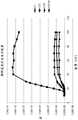
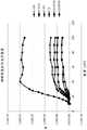
图5是表明C3HF4N的电子碰撞电离能对比物种浓度的曲线图;Figure 5is a graph showing electron impact ionization energy versus species concentration forC3HF4N ;
图6是表明C2HF2N的电子碰撞电离能对比物种浓度的曲线图;Figure 6is a graph showing electron impact ionization energy versus species concentration forC2HF2N ;
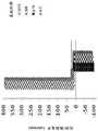
图7是表明从C3HF4N沉积的聚合膜的元素含量的X射线光电子光谱曲线图;Figure 7 isa graph of X-ray photoelectron spectroscopy showing the elemental content of polymeric films deposited fromC3HF4N ;
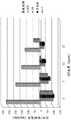
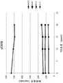
图8是表明使用C2HF2N和O2的随氧气流速变化的SiO、SiN、p-Si和a-C膜的沉积或蚀刻速率的曲线图;Figure 8is a graph showing deposition or etch rates of SiO, SiN, p-Si andaC films as a function of oxygen flow rate usingC2HF2N and O2;
图9是表明使用C3HF4N和O2的随氧气流速变化的SiO、SiN、p-Si和a-C膜的沉积或蚀刻速率的曲线图;Figure 9 is a graph showingdeposition or etch rates of SiO, SiN, p-Si and aC films as a function of oxygen flow rate usingC3HF4N andO2 ;
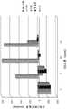
图10是表明使用C3HF4N和CF4的随氧气流速变化的SiO、SiN、p-Si和a-C膜的蚀刻速率的曲线图;Figure 10 isa graph showing etch rates of SiO, SiN, p-Si and aC films as a function of oxygen flow rate usingC3HF4N andCF4 ;
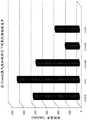
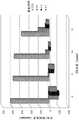
图11是比较了没有氧气添加的情况下的C3HF4N、C2HF2N、C5F5N、C2F3N、cC4F8、以及C4F6的氧化硅沉积和蚀刻速率的曲线图;Figure 11 compares the silicon oxide deposition of C3 HF4 N, C2 HF2 N, C5 F5 N, C2 F3 N, cC4 F8 , and C4 F6 without oxygen addition and etch rate graphs;
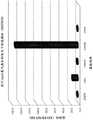
图12是比较了没有氧气添加的情况下的C3HF4N、C2HF2N、C5F5N、C2F3N、cC4F8、以及C4F6的氧化硅比氮化硅的选择性的曲线图;Figure 12 compares the silicon oxide ratio of C3 HF4 N, C2 HF2 N, C5 F5 N, C2 F3 N, cC4 F8 , and C4 F6 without oxygen addition A graph of the selectivity of silicon nitride;
图13是比较了在5sccm氧气添加的情况下的C3HF4N、C2HF2N、C5F5N、C2F3N、cC4F8、以及C4F6的氧化硅蚀刻速率的曲线图;Figure 13 is a comparison of C3 HF4 N, C2 HF2 N, C5 F5 N, C2 F3 N, cC4 F8 , and C4 F6 silicon oxide in the case of 5 sccm oxygen addition Graph of etch rate;
图14是比较了在5sccm氧气添加的情况下的C3HF4N、C2HF2N、C5F5N、C2F3N、cC4F8、以及C4F6的氧化硅比氮化硅的选择性的曲线图;Figure 14 compares the silicon oxides of C3 HF4 N, C2 HF2 N, C5 F5 N, C2 F3 N, cC4 F8 , and C4 F6 in the case of 5 sccm oxygen addition A graph of the selectivity to silicon nitride;
图15是比较了在10sccm氧气添加的情况下的C3HF4N、C2HF2N、C5F5N、C2F3N、cC4F8、以及C4F6的氧化硅蚀刻速率的曲线图;Figure 15 compares the silicon oxides of C3 HF4 N, C2 HF2 N, C5 F5 N, C2 F3 N, cC4 F8 , and C4 F6 in the case of 10 sccm oxygen addition Graph of etch rate;
图16是比较了在10sccm氧气添加的情况下的C3HF4N、C2HF2N、C5F5N、C2F3N、cC4F8、以及C4F6的氧化硅比氮化硅的选择性的曲线图;Figure 16 compares the silicon oxides of C3 HF4 N, C2 HF2 N, C5 F5 N, C2 F3 N, cC4 F8 , and C4 F6 in the case of 10 sccm oxygen addition A graph of the selectivity to silicon nitride;
图17是比较了在15sccm氧气添加的情况下的C3HF4N、C2HF2N、C2F3N、cC4F8、以及C4F6的氧化硅蚀刻速率的曲线图;Figure 17 isa graph comparing silicon oxide etch ratesofC3HF4N ,C2HF2N ,C2F3N, cC4F8, andC4F6 with15 seem oxygen addition;
图18是比较了在15sccm氧气添加的情况下的C3HF4N、C2HF2N、C2F3N、cC4F8、以及C4F6的氧化硅比氮化硅的选择性的曲线图;Figure 18 compares the choice of silicon oxide to silicon nitride for C3 HF4 N, C2 HF2 N, C2 F3 N, cC4 F8 , and C4 F6 in the case of 15 sccm oxygen addition Sexual graphs;
图19是表明添加N2对不同基板材料的cC4F8和O2蚀刻速率的影响的曲线图;Figure 19 is a graph showing the effectofN addition oncC4F8 andO2 etch rates for different substrate materials;
图20是表明将O2添加到cC4F8和NH3中对不同基板材料的沉积和蚀刻速率的影响的曲线图;Figure 20 is a graph showing the effect of addingO2 tocC4F8 andNH3 on the deposition and etch rates of different substrate materials;
图21是表明C2F3N的电子碰撞电离能对比物种浓度的曲线图;Figure 21 is a graph showing electron impact ionization energy versus species concentration forC2F3N;
图22是表明使用C2F3N和O2的随氧气流速变化的SiO、SiN、p-Si和a-C膜的蚀刻速率的曲线图;Figure 22is a graph showing etch rates of SiO, SiN, p-Si and aC films as a function of oxygen flow rate usingC2F3N andO2 ;
图23是表明C3H3F6N的电子碰撞电离数据对比能量的曲线图;并且Figure 23is a graph showing electron impact ionization data versus energy forC3H3F6N ;and
图24是表明在不同的基板材料上没有氧气添加的情况下的C3H3F6N的沉积和蚀刻速率的曲线图。Figure 24 is a graph showing deposition and etch ratesofC3H3F6N on various substrate materials without oxygen addition.
具体实施方式Detailed ways
披露了用于在含硅膜中等离子体蚀刻半导体结构(诸如通道孔洞、栅极沟槽、阶梯式接点、电容器孔洞、接触孔洞等)的方法。所披露的方法包括以下步骤:i)将含氮蚀刻化合物的蒸气引入基板上含有含硅膜的反应腔室中,其中该含氮蚀刻化合物是含有至少一个C≡N或C=N官能团的有机氟化合物;ii)将惰性气体引入该反应腔室中;并且iii)活化等离子体以产生能够从该基板蚀刻该含硅膜的经活化的含氮蚀刻化合物。在此,这些有机氟化合物是含有碳-氟(C-F)键的有机化合物。Methods for plasma etching semiconductor structures, such as via holes, gate trenches, stepped contacts, capacitor holes, contact holes, etc., in silicon-containing films are disclosed. The disclosed method comprises the steps of: i) introducing a vapor of a nitrogen-containing etching compound into a reaction chamber containing a silicon-containing film on a substrate, wherein the nitrogen-containing etching compound is an organic compound containing at least one C≡N or C=N functional group fluorine compound; ii) introducing an inert gas into the reaction chamber; and iii) activating a plasma to produce an activated nitrogen-containing etch compound capable of etching the silicon-containing film from the substrate. Here, these organic fluorine compounds are organic compounds containing carbon-fluorine (C-F) bonds.
所披露的包含至少一个C≡N官能团的有机氟化合物具有以下通式:The disclosed organofluorine compounds comprising at least one C≡N functional group have the general formula:
N≡C-R1 (I)N≡CR1 (I)
(N≡C-)(R2)(-C≡N) (II)(N≡C-)(R2 )(-C≡N) (II)
其中R1是具有式HaFbCc的官能团,其中a=1-11,b=1-11,并且c=0-5,并且R2是具有式HaFbCc的官能团,其中a=0-11,b=1-11,并且c=0-5。该HaFbCc官能团可以是直链的、支链的或环状的并且饱和的或不饱和的。申请人相信,与CxFy聚合物(其中x在从0.01至1的范围内并且y在从0.01至4的范围内)相比,C≡N官能度可以提供改进的抗蚀刻聚合物沉积益处。当该有机氟化合物包括至少一个H时,可以在维持对掩模层的高选择性的同时提高SiN的蚀刻速率。whereinR is a functional group having the formula Ha Fb Cc , wherein a = 1-11, b = 1-11, and c = 0-5, andR is a functional group having the formula Ha Fb Cc , where a=0-11, b=1-11, and c=0-5. The Ha Fb Cc functional group may be linear, branched or cyclic and saturated or unsaturated. Applicants believe that C≡N functionality can provide improved etch resistant polymer deposition compared toCxFy polymers (where x ranges from 0.01 to 1 and y ranges from0.01 to 4) benefit. When the organic fluorine compound includes at least one H, the etching rate of SiN can be increased while maintaining high selectivity to the mask layer.
所披露的包含至少一个C=N官能团的有机氟化合物具有以下通式:The disclosed organofluorine compounds comprising at least one C=N functional group have the general formula:
R1x[-C=N(R2z)]y (III)R1x [-C=N(R2z )]y (III)
其中x=1-2,y=1-2,z=0-1,x+z=1-3,并且每个R1和R2独立地具有式HaFbCc,其中a=0-11,b=0-11,并且c=0-5。该HaFbCc官能团可以是直链的、支链的或环状的并且饱和的或不饱和的。申请人相信,与CxFy聚合物(其中x在从0.01至1的范围内并且y在从0.01至4的范围内)相比,C=N官能度可以提供改进的在硅层之间的选择性。当该有机氟化合物包括至少一个H时,并且优选地当R2是H时,可以在维持对掩模层的高选择性的同时提高SiN的蚀刻速率。where x=1-2, y=1-2, z=0-1, x+z=1-3, and each R1 and R2 independently has the formula Ha Fb Cc where a=0 -11, b=0-11, and c=0-5. The Ha Fb Cc functional group may be linear, branched or cyclic and saturated or unsaturated. Applicants believe that the C=N functionality can provide improved in- between silicon layers compared toCxFy polymers (where x ranges from 0.01 to 1 and y ranges from 0.01 to 4). selectivity. When the organofluorine compound includes at least one H, and preferably whenR2 is H, the etch rate of SiN can be increased while maintaining high selectivity to the mask layer.
所披露的有机氟化合物可以是含有至少一个C≡N或C=N官能团的氢氟烃(CxHyFz)或氟碳化合物(CmFn),或含有至少一个C≡N或C=N官能团的杂氢氟烃(CxHyFz)或杂氟碳化合物(CmFn),其中m、n、x、y和z是整数。The disclosed organofluorine compounds may be hydrofluorocarbons (Cx Hy Fz ) or fluorocarbons (Cm Fn ) containing at least one C≡N or C=N functional group, or containing at least one C≡N or Heterohydrofluorocarbons (CxHyFz ) or heterofluorocarbons (CmFn ) with C=N functional groups,wherem , n, x, y and z are integers.
所披露的含氮蚀刻化合物包括:二氟乙腈(C2HF2N)、2,3,3,3-四氟丙腈(C3HF4N)、2,2,3,3-四氟丙腈(C3HF4N)或六氟丙酮亚胺(C3HF6N),其在表2中列出。这些分子是可商购的,并且它们的结构式、CAS编号和沸点也包括在表2中。The disclosed nitrogen-containing etching compounds include: difluoroacetonitrile (C2 HF2 N), 2,3,3,3-tetrafluoropropionitrile (C3 HF4 N), 2,2,3,3-tetrafluoro Propionitrile (C3 HF4 N) or hexafluoroacetonimine (C3 HF6 N), which are listed in Table 2. These molecules are commercially available and their structural formulas, CAS numbers and boiling points are also included in Table 2.
表2.可商购的蚀刻化合物Table 2. Commercially Available Etching Compounds


所披露的含氮蚀刻化合物还可以包括4,4,4-三氟巴豆腈(C4H2F3N);3,3,3-三氟丙腈(C3H2F3N);氟乙腈(C2H2FN);八氟己烷-1,6-二腈(C6F8N2);1,1-双(三氟甲基)-2,2-二氰基乙烯(C6F6N2);N,1,1,1,3,3,3-七氟-丙胺(C3F7N);1,1,1,6,6,6-六氟-3-氮杂己-3-烯(C5H5F6N)。它们的结构式、CAS编号和沸点或预测的沸点也包括在表2中。本领域普通技术人员将认识到,可以使用所提供的CAS编号获得这些化合物的合成方法。The disclosed nitrogen-containing etching compounds may also include 4,4,4-trifluorocrotononitrile (C4 H2 F3 N); 3,3,3-trifluoropropionitrile (C3 H2 F3 N); Fluoroacetonitrile (C2 H2 FN); Octafluorohexane-1,6-dinitrile (C6 F8 N2 ); 1,1-bis(trifluoromethyl)-2,2-dicyanoethylene (C6 F6 N2 ); N,1,1,1,3,3,3-heptafluoro-propylamine (C3 F7 N); 1,1,1,6,6,6-hexafluoro- 3-Azahex-3-ene (C5 H5 F6 N). Their structural formulas, CAS numbers and boiling points or predicted boiling points are also included in Table 2. Those of ordinary skill in the art will recognize that synthetic methods for these compounds can be obtained using the provided CAS numbers.
所披露的含氮蚀刻化合物可以在高纵横比结构(诸如具有在从10:1至200:1范围内的纵横比的那些,诸如DRAM和3D NAND应用)中提供对于掩模层、蚀刻终止层和器件通道材料的高选择性并且没有轮廓变形。可替代地,所披露的含氮蚀刻化合物还可以在接触蚀刻应用中提供对于掩模层或氮化硅,诸如具有在从1:1至50:1的范围内的纵横比的那些,的高选择性。The disclosed nitrogen-containing etch compounds can provide for masking layers, etch stop layers in high aspect ratio structures such as those having aspect ratios ranging from 10:1 to 200:1, such as DRAM and 3D NAND applications. and high selectivity of device channel materials without profile distortion. Alternatively, the disclosed nitrogen-containing etch compounds can also provide high sensitivity to mask layers or silicon nitride, such as those having aspect ratios ranging from 1:1 to 50:1, in contact etch applications. selective.
所披露的含氮蚀刻化合物可提供对于宽的蚀刻工艺条件的无限选择性。在此,选择性是指两个不同层的蚀刻速率比。例如,SiO层对比a-C层的选择性是SiO的蚀刻速率除以a-C层的蚀刻速率。所披露的含氮蚀刻化合物可以在图案高纵横比结构中提供在这些含硅膜与掩模材料之间的改进的选择性、对通道区域的较小损害以及减少的弯曲。所披露的含氮蚀刻化合物还可以蚀刻穿过p-Si、SiO和/或SiN的交替层,导致垂直蚀刻轮廓(即,表明在交替层之间的在从2:1至1:2的范围内的选择性)。The disclosed nitrogen-containing etch compounds can provide unlimited selectivity over a wide range of etch process conditions. Here, selectivity refers to the ratio of etching rates of two different layers. For example, the selectivity of the SiO layer over the a-C layer is the etch rate of SiO divided by the etch rate of the a-C layer. The disclosed nitrogen-containing etch compounds can provide improved selectivity between these silicon-containing films and mask materials, less damage to channel regions, and reduced bowing in patterned high aspect ratio structures. The disclosed nitrogen-containing etch compounds can also etch through alternating layers of p-Si, SiO, and/or SiN, resulting in a vertical etch profile (i.e., indicating a range from 2:1 to 1:2 between alternating layers). selectivity within).
所披露的含氮蚀刻化合物以大于95%v/v纯度、优选以大于99.99%v/v纯度、并且更优选以大于99.999%v/v纯度提供。所披露的含氮蚀刻化合物含有按体积计小于5%的痕量气体杂质,其中按体积计小于150ppm的杂质气体,诸如N2和/或H2O和/或CO2,包含在所述痕量气态杂质中。优选地,该等离子体蚀刻气体中的水含量是按重量计小于20ppmw。可通过蒸馏和/或使气体或液体通过适合的吸附剂(诸如4A分子筛)产生经纯化的产物。The disclosed nitrogen-containing etch compounds are provided in greater than 95% v/v purity, preferably greater than 99.99% v/v purity, and more preferably greater than 99.999% v/v purity. The disclosed nitrogen-containing etch compounds contain less than 5% by volume of trace gas impurities, wherein less than 150 ppm by volume of impurity gases, such asN2 and/orH2O and/orCO2 , are contained in the traces amount of gaseous impurities. Preferably, the water content in the plasma etching gas is less than 20 ppmw by weight. Purified products can be produced by distillation and/or passing a gas or liquid through a suitable adsorbent, such as 4A molecular sieves.
所披露的含氮蚀刻化合物含有小于10%v/v、优选地小于1%v/v、更优选小于0.1%v/v、并且甚至更优选地小于0.01%v/v的任何其异构体,其可以通过蒸馏气体或液体以移除异构体来纯化并且可以提供更好的工艺可重复性。The disclosed nitrogen-containing etch compounds contain less than 10% v/v, preferably less than 1% v/v, more preferably less than 0.1% v/v, and even more preferably less than 0.01% v/v of any of its isomers , which can be purified by distillation of gas or liquid to remove isomers and can provide better process reproducibility.
可替代地,所披露的含氮蚀刻化合物可含有在5%v/v与50%v/v之间的其异构体,特别地当该异构体混合物提供改进的工艺参数或如果目标异构体的分离过于困难或昂贵时。例如,所披露的含氮蚀刻化合物可包含在大约50%v/v与大约75%v/v之间的2,3,3,3-四氟丙腈以及在大约25%v/v与大约50%v/v之间的2,2,3,3-四氟丙腈。该异构体混合物可减少对于两个或更多个通向该反应腔室的气体管线的需要。Alternatively, the disclosed nitrogen-containing etch compounds may contain between 5% v/v and 50% v/v of their isomers, particularly when the isomer mixture provides improved process parameters or if the target isomer When the separation of the conformers is too difficult or expensive. For example, the disclosed nitrogen-containing etch compounds may comprise between about 50% v/v and about 75% v/v 2,3,3,3-tetrafluoropropionitrile and between about 25% v/v and about Between 50% v/v 2,2,3,3-tetrafluoropropionitrile. The isomer mixture can reduce the need for two or more gas lines to the reaction chamber.
一些披露的含氮蚀刻化合物在室温和大气压力下是气态的。对于非气态(即液体或固体)化合物,可通过经由常规的汽化步骤,诸如直接汽化或通过用惰性气体(N2、Ar、He)鼓泡使这些化合物汽化来产生它们的气体形式。这些非气态化合物可在引入反应器中之前以液态进料到汽化器中,在该汽化器中使其汽化。Some of the disclosed nitrogen-containing etch compounds are gaseous at room temperature and atmospheric pressure. For non-gaseous (ie liquid or solid) compounds, their gaseous form can be produced by vaporizing these compounds via conventional vaporization procedures, such as direct vaporization or by bubbling these compounds with inert gases (N2, Ar, He). These non-gaseous compounds may be fed in liquid state to a vaporizer where they are vaporized prior to introduction into the reactor.
所披露的含氮蚀刻化合物适合于在这些含硅膜中等离子体蚀刻半导体结构(诸如通道孔洞、栅极沟槽、阶梯式接点、电容器孔洞、接触孔洞等)。所披露的含氮蚀刻化合物不仅与当前可获得的掩模材料相容,而且与未来几代掩模材料相容,因为所披露的含氮蚀刻化合物对掩模连同高纵横比结构的良好轮廓引起极少损害或没有损害。换句话说,所披露的含氮蚀刻化合物可产生具有最小至没有弯曲、图案坍塌或粗糙度的垂直的蚀刻图案。为了实现这些特性,所披露的含氮蚀刻化合物可以在蚀刻期间沉积抗蚀刻聚合物层,以帮助减少在该蚀刻工艺期间的氧和氟自由基的直接影响。所披露的含氮蚀刻化合物还可以减少在蚀刻期间对p-Si或结晶Si通道结构的损害。优选地,披露的含氮蚀刻化合物在用于递送到该反应器/腔室中的蚀刻工艺期间是适合地挥发性的且稳定的。The disclosed nitrogen-containing etch compounds are suitable for plasma etching semiconductor structures (such as via holes, gate trenches, stepped contacts, capacitor holes, contact holes, etc.) in these silicon-containing films. The disclosed nitrogen-containing etch compounds are compatible not only with currently available mask materials, but also with future generations of mask materials because the disclosed nitrogen-containing etch compounds induce good profile of the mask as well as high aspect ratio structures. Little or no damage. In other words, the disclosed nitrogen-containing etch compounds can produce vertical etch patterns with minimal to no bowing, pattern collapse, or roughness. To achieve these properties, the disclosed nitrogen-containing etch compounds can deposit an etch-resistant polymer layer during etching to help reduce the direct impact of oxygen and fluorine radicals during the etching process. The disclosed nitrogen-containing etch compounds can also reduce damage to p-Si or crystalline Si channel structures during etching. Preferably, the disclosed nitrogen-containing etch compounds are suitably volatile and stable during the etch process for delivery into the reactor/chamber.
材料相容性测试对于确定是否任何所披露的含氮蚀刻化合物将与腔室材料反应并且降低具有短期或长期用途的腔室的性能是重要的。在腔室、阀等的部件中涉及的关键材料包括不锈钢、铝、镍、PCTFE、PVDF、PTFE和其他金属和聚合物。有时,这些材料暴露于高温(例如高于20℃)和高压(例如高于1atm),这可增强其降解。计量方法可以包括目视检查、重量测量、测量扫描电子显微术(SEM)中的纳米尺度变化、拉伸强度、硬度等。Material compatibility testing is important to determine if any of the disclosed nitrogen-containing etch compounds will react with chamber materials and degrade chamber performance for short or long term use. Key materials involved in components of chambers, valves, etc. include stainless steel, aluminum, nickel, PCTFE, PVDF, PTFE, and other metals and polymers. Sometimes these materials are exposed to high temperature (eg, above 20°C) and high pressure (eg, above 1 atm), which can enhance their degradation. Metrology methods may include visual inspection, gravimetric measurements, measuring nanoscale changes in scanning electron microscopy (SEM), tensile strength, hardness, and the like.
所披露的含氮蚀刻化合物可用于等离子体蚀刻在基板上的含硅膜。所披露的等离子体蚀刻方法可以在制造半导体器件,诸如NAND或3D NAND门或者闪存或DRAM存储器或晶体管,诸如鳍形场效应晶体管(FinFET),块状互补金属氧化物半导体(块状CMOS),完全耗尽型绝缘体上硅(FD-SOI)结构上是有用的。所披露的含氮蚀刻化合物可用于其他应用领域,诸如不同的前段制程(FEOL)和后段制程(BEOL)蚀刻应用。此外,所披露的含氮蚀刻化合物还可以用于在3D硅通孔(TSV)蚀刻应用中蚀刻Si用于将存储器与在基板上的逻辑电路互相连接。The disclosed nitrogen-containing etch compounds are useful for plasma etching silicon-containing films on substrates. The disclosed plasma etching method can be used in the fabrication of semiconductor devices such as NAND or 3D NAND gates or flash memory or DRAM memories or transistors such as fin field effect transistors (FinFETs), bulk complementary metal oxide semiconductors (bulk CMOS), Fully depleted silicon-on-insulator (FD-SOI) is structurally useful. The disclosed nitrogen-containing etch compounds can be used in other application areas, such as various front-end-of-line (FEOL) and back-end-of-line (BEOL) etch applications. In addition, the disclosed nitrogen-containing etch compounds can also be used to etch Si in 3D through-silicon via (TSV) etch applications for interconnecting memory with logic circuitry on a substrate.
该等离子体蚀刻方法包括提供具有基板安置在其中的反应腔室。该反应腔室可以是其中进行蚀刻方法的器件内的任何附件或腔室,诸如并且不限于反应性离子蚀刻(RIE)、具有单一或多个频率RF源的电容耦合等离子体(CCP)、电感耦合等离子体(ICP)、或微波等离子体反应器,或能够选择性地移除含硅膜的一部分或产生活性物种的其他类型的蚀刻系统。本领域普通技术人员将认识到,不同的等离子体反应腔室设计提供不同的电子温度控制。合适的可商购的等离子体反应腔室包括但不限于以商标eMAXTM出售的应用材料公司(Applied Materials)磁增强的反应性离子蚀刻器或以商标
可替代地,等离子体处理过的反应物可以在反应腔室外产生。MKS仪器公司的
该反应腔室可含有一个或多于一个基板。例如,该反应腔室可含有从1至200个具有从25.4mm至450mm的直径的硅晶圆。基板可为任何适用于制造半导体、光伏材料、平板或LCD-TFT器件的基板。合适的基板的实例包括晶圆,如硅、二氧化硅、玻璃、或GaAs晶圆。从先前的制造步骤,该晶圆将具有在其上的多个膜或层,包括含硅膜或层。这些层可以是图案化的或可以不是图案化的。合适的层的实例包括但不限于硅(诸如非晶硅、p-Si、结晶硅、其中的任何一种可以进一步用B、C、P、As、和/或Ge进行p掺杂或n掺杂)、二氧化硅、氮化硅、氧化硅、氮氧化硅、SiaObHcCdNe(其中a>0;b、c、d、e≥0)、掩模层材料(诸如无定形碳、减反射涂层、光致抗蚀剂材料、钨、氮化钛、氮化钽或其组合)、蚀刻终止层材料(诸如氮化硅、多晶硅、结晶硅、碳化硅、SiCN或其组合)、器件通道材料(诸如结晶硅、外延硅、掺杂硅、SiaObHcCdNe(其中a>0;b、c、d、e≥0)或其组合)。该氧化硅层可以形成介电材料,诸如基于有机物或基于氧化硅的低k介电材料(例如,多孔SiCOH膜)。示例性的低k介电材料以商品名Black DiamondII或III由应用材料公司出售。此外,可以使用包含钨或贵金属(例如铂、钯、铑或金)的层。此外,这些含硅膜的实例可以是SiaObHcCdNe(其中a>0;b、c、d、e≥0)。贯穿本说明书和权利要求书,晶圆和其上的任何相关层称为基板。The reaction chamber may contain one or more than one substrate. For example, the reaction chamber may contain from 1 to 200 silicon wafers having a diameter of from 25.4 mm to 450 mm. The substrate can be any substrate suitable for use in the manufacture of semiconductor, photovoltaic, flat panel or LCD-TFT devices. Examples of suitable substrates include wafers, such as silicon, silicon dioxide, glass, or GaAs wafers. From previous fabrication steps, the wafer will have a plurality of films or layers thereon, including silicon-containing films or layers. These layers may or may not be patterned. Examples of suitable layers include, but are not limited to, silicon (such as amorphous silicon, p-Si, crystalline silicon, any of which can be further p-doped or n-doped with B, C, P, As, and/or Ge). heterogeneous), silicon dioxide, silicon nitride, silicon oxide, silicon oxynitride, Sia Ob Hc CdNe (where a>0; b, c, d, e≥0), mask layer material ( materials such as amorphous carbon, antireflective coatings, photoresist materials, tungsten, titanium nitride, tantalum nitride or combinations thereof), etch stop layer materials such as silicon nitride, polysilicon, crystalline silicon, silicon carbide, SiCN or a combination thereof), device channel materials (such as crystalline silicon, epitaxial silicon, doped silicon, Sia Ob Hc CdNe (where a>0; b, c, d, e≥0) or a combination thereof) . The silicon oxide layer may form a dielectric material, such as an organic-based or silicon oxide-based low-k dielectric material (eg, a porous SiCOH film). Exemplary low-k dielectric materials are sold by Applied Materials under the trade designation Black Diamond II or III. Furthermore, layers comprising tungsten or noble metals such as platinum, palladium, rhodium or gold may be used. Furthermore, examples of these silicon-containing films may be Sia Ob Hc CdNe (where a>0; b, c, d, e≥0). Throughout this specification and claims, a wafer and any associated layers thereon are referred to as a substrate.
以下是可以将所披露的含氮蚀刻化合物施加在其上进行蚀刻的基板的示例性实施例。The following are exemplary examples of substrates on which the disclosed nitrogen-containing etch compounds may be applied for etching.
在一个实施例中,基板100可以包括多个层的堆叠,如图1a中示出的。图1a是产生3D NAND门的3D NAND堆叠中的示例性层的截面侧视图。在图1a中,七个交替的SiO/SiN(即,104a/104b)层的堆叠104位于硅晶圆102的顶部上(即,ONON或TCAT技术)。本领域的普通技术人员将认识到一些技术用p-Si层替换SiN层104a(例如,SiO/p-Si或P-BICS技术)。无定形碳(a-C)掩模层106位于七个SiO/SiN层104的顶部上。a-C掩模层106可以含有C和H以及其他元素诸如硼、氮等,以改进在SiO/SiN层蚀刻期间的抗蚀刻性。减反射涂层108位于a-C掩模层106的顶部上。图案化的光致抗蚀剂层110位于减反射涂层108的顶部上。在此,在减反射涂层108与a-C掩模层106之间可以存在SiON层(未示出),以将光致抗蚀剂层110中的图案转移到a-C层106。本领域的普通技术人员将认识到,图1a中的基板100中的层的堆叠仅出于示例性目的而提供,并且所披露的含氮蚀刻化合物可用于蚀刻其他类型的层的堆叠。此外,本领域的普通技术人员将认识到,基板100的堆叠中的交替的SiO/SiN或SiO/p-Si层104的数目可以变化(即,可以包括多于或少于所描绘的七个SiO/SiN(104a/104b)层)。In one embodiment, the
图1b是3D NAND堆叠中的示例性层的截面侧视图,示出了在蚀刻期间沉积在侧壁上的聚合物。所披露的含氮化合物可以在等离子体工艺期间产生适合于各向异性蚀刻含硅膜104并且在正蚀刻的结构的侧壁上沉积含N聚合物钝化层212两者的碎片,如图1b中示出的。在图1b与图1a之间的差异是,在图1b中,通孔214通过使用所披露的含氮蚀刻化合物的等离子体蚀刻而在基板100中形成,这些化合物还将聚合物钝化层212沉积在通孔214的侧壁上。聚合物钝化层212还在通孔214的底部处提供了更平滑的侧壁、较少的弯曲和较少的变形。然而,聚合物钝化层212可以通过本领域已知的干或湿蚀刻化学过程容易地移除或清洁。Figure 1b is a cross-sectional side view of exemplary layers in a 3D NAND stack showing polymer deposited on the sidewalls during etching. The disclosed nitrogen-containing compounds can generate fragments during a plasma process suitable for both anisotropically etching the silicon-containing
图1c是3D NAND堆叠中的示例性层的截面侧视图,示出了在3D NAND堆叠中的交替SiO/SiN层蚀刻期间产生的颗粒316。如图1c中示出的,在交替的SiO/SiN(即,104a/104b)层104的侧壁上产生的颗粒316可以通过使用所披露的含氮化合物来最小化。在图1c与图1b之间的差异是,在图1c中,交替的SiO/SiN暴露的侧壁具有在等离子体蚀刻期间产生的颗粒316。申请人不认为所披露的含氮化合物将产生图1c中示出的颗粒316。Figure 1c is a cross-sectional side view of exemplary layers in a 3D NAND
图1d是3D NAND堆叠中的示例性层的截面侧视图,示出了在蚀刻之后在3D NAND堆叠的侧壁上暴露的SiN的选择性蚀刻。堆叠100中的SiN暴露的侧壁可以通过以下方式选择性地蚀刻,如图1d中示出的:使用所披露的含氮化合物来选择性地破坏SiN层104b中的Si-N键(相比于SiO层104a中的Si-O键),在通孔214中的SiO/SiN层104的堆叠上形成选择性侧壁SiN蚀刻418。在图1d与图1b之间的差异是,在图1d中,通过所披露的含氮化合物来选择性地蚀刻交替的SiO/SiN侧壁上暴露的SiN,形成选择性侧壁SiN蚀刻418。典型地,选择性侧壁SiN蚀刻418通过使用与磷酸的混合物的湿法蚀刻来进行。已知用干式等离子体蚀刻工艺替换湿式蚀刻工艺来大大改进半导体器件制造工艺的经济性,因为湿式蚀刻要求将基板移动至不同的湿式蚀刻设备。用所披露的方法,可以在一个蚀刻设备中进行包括选择性侧壁SiN蚀刻的所有蚀刻,这可以减少半导体制造的成本。Figure Id is a cross-sectional side view of exemplary layers in a 3D NAND stack showing selective etching of exposed SiN on sidewalls of the 3D NAND stack after etching. The exposed sidewalls of the SiN in the
在替代实施例中,基板100可以包括在其上的多个层的堆叠,如图2中示出的。图2是产生DRAM存储器的DRAM堆叠中的示例性层的截面侧视图。在图2中,四层的堆叠位于硅晶圆102的顶部上。a-C掩模层106位于大SiO层104a的顶部上。减反射涂层108位于a-C掩模106的顶部上。图案光致抗蚀剂层110位于减反射涂层108的顶部上。在此,在减反射涂层108与a-C掩模层106之间可以存在SiON层(未示出),以将光致抗蚀剂层110中的图案转移到a-C层106。本领域的普通技术人员将认识到,图2中的层的堆叠仅出于示例性目的而提供,并且所披露的含氮蚀刻化合物可用于蚀刻其他层的堆叠,例如,对于其中用TiN层替换a-C掩模层106的堆叠。此外,本领域的普通技术人员将认识到,该堆叠中的层数可以变化(即,可以包括多于或少于所描绘的层)。In alternative embodiments, the
图3a是示例性层的截面侧视图,示出了在围绕典型的晶体管器件区域的SiO绝缘层上的产生晶体管结构的光致抗蚀剂图案。如图3a中示出的,基板600可以包括围绕支撑在硅晶圆602上的晶体管栅极电极区域的四层的堆叠。图3a中示出的晶体管区域包括充当源极和漏极的两个掺杂的硅区域606。晶体管栅极电介质614存在于栅极电极616下面。整个晶体管(即,晶体管栅极电介质614和栅极电极616)被薄的SiN层608围绕,该SiN层可以稍后在接触蚀刻期间充当蚀刻终止层。每个晶体管器件区域616/606被硅晶圆602中的SiO隔离区域604分开以使电干扰最小化。本领域的普通技术人员将认识到,层602可以位于绝缘体上硅(SOI)晶圆的氧化硅层的顶部上。另一个SiO层610被沉积在晶体管上并用于使金属接点与晶体管器件区域606绝缘。使用光致抗蚀剂掩模612来图案化SiO层610。在等离子体环境中使用所披露的含氮蚀刻化合物进行蚀刻。在此,光致抗蚀剂充当蚀刻SiO层610的掩模,并且在SiN层608上停止蚀刻,如图3b中示出的。Figure 3a is a cross-sectional side view of exemplary layers showing a photoresist pattern on a SiO insulating layer surrounding a typical transistor device region to create a transistor structure. As shown in FIG. 3 a , the
图3b是在蚀刻该SiO绝缘层之后的图3a的示例性层的截面侧视图。在图3b与图3a之间的差异是,在图3b中,通过经由所披露的含氮化合物的蚀刻在SiO层610中形成通孔718。SiO层610可以用光致抗蚀剂层612作为掩模层进行蚀刻。该掩模层可以是任何合适的光致抗蚀剂掩模材料,诸如TiN、a-C等。可以在下面的SiN层608处停止该蚀刻。Figure 3b is a cross-sectional side view of the exemplary layer of Figure 3a after etching the SiO insulating layer. The difference between FIG. 3b and FIG. 3a is that in FIG. 3b vias 718 are formed in
所披露的含氮蚀刻化合物还可以用于用不同的等离子体条件和不同的混合物来蚀刻SiN层608。本领域的普通技术人员将认识到,图3a和图3b中的层的堆叠和几何形状仅出于示例性目的而提供,并且所披露的含氮蚀刻化合物可用于蚀刻其他类型的层的堆叠。此外,本领域的普通技术人员将认识到,该堆叠中的层数可以变化(即,可以包括多于或少于所描绘的四个层)。The disclosed nitrogen-containing etch compounds can also be used to etch
将所披露的含氮蚀刻化合物的蒸气引入含有该基板和含硅膜的反应腔室中。可以以在从大约0.1sccm至大约1slm范围内的流速将该蒸气引入该腔室中。例如,对于200mm晶圆尺寸,可以以在从大约5sccm至大约50sccm范围内的流速将该蒸气引入该腔室中。可替代地,对于450mm晶圆尺寸,可以以在从大约25sccm至大约250sccm范围内的流速将该蒸气引入该腔室中。本领域普通技术人员将认识到,流速可以随工具不同而不同。A vapor of the disclosed nitrogen-containing etch compound is introduced into a reaction chamber containing the substrate and silicon-containing film. The vapor may be introduced into the chamber at a flow rate ranging from about 0.1 sccm to about 1 slm. For example, for a 200mm wafer size, the vapor may be introduced into the chamber at a flow rate ranging from about 5 seem to about 50 seem. Alternatively, for a 450mm wafer size, the vapor may be introduced into the chamber at a flow rate ranging from about 25 seem to about 250 seem. Those of ordinary skill in the art will recognize that flow rates can vary from tool to tool.
所披露的含氮蚀刻化合物可以以纯净形式或与惰性气体(诸如N2、Ar、He、Xe等)或溶剂的共混物供应。所披露的含氮蚀刻化合物可以是以变化浓度存在于该共混物中。对于液体含氮化合物,可通过经由常规的汽化步骤,诸如直接汽化或通过鼓泡使纯净的或共混的含氮蚀刻化合物溶液汽化来产生这些含氮蚀刻化合物的蒸气形式。这些纯净的或共混的含氮蚀刻化合物可在引入反应器中之前以液态进料到汽化器中,在该汽化器中使其汽化。The disclosed nitrogen-containing etch compounds may be supplied in neat form or in blends with inert gases (such asN2 , Ar, He, Xe, etc.) or solvents. The disclosed nitrogen-containing etch compounds can be present in the blend in varying concentrations. For liquid nitrogen-containing compounds, vaporized forms of these nitrogen-containing etch compounds can be produced by vaporizing neat or blended nitrogen-containing etch compound solutions by conventional vaporization procedures, such as direct vaporization or by bubbling. These nitrogen-containing etch compounds, neat or blended, may be fed in liquid state to a vaporizer where they are vaporized prior to introduction into the reactor.
可替代地,可通过将载气传送至含有所披露的含氮蚀刻化合物的容器内或通过将载气鼓泡进所披露的含氮化合物内使这些纯净的或共混的含氮蚀刻化合物汽化。该载气可包括但不限于Ar、He、N2及其混合物。用载气鼓泡还可移除这些纯净的或共混的含氮蚀刻化合物溶液中存在的任何溶解氧。该载气和所披露的含氮蚀刻化合物然后作为蒸气被引入反应器中。Alternatively, these nitrogen-containing etch compounds, neat or blended, can be vaporized by delivering a carrier gas into a vessel containing the disclosed nitrogen-containing etch compounds or by bubbling a carrier gas into the disclosed nitrogen-containing compounds . The carrier gas may include, but is not limited to, Ar, He,N2 , and mixtures thereof. Bubbling with a carrier gas also removes any dissolved oxygen present in these neat or blended nitrogen-containing etch compound solutions. The carrier gas and the disclosed nitrogen-containing etch compound are then introduced into the reactor as a vapor.
必要时,含有所披露的含氮蚀刻化合物的容器可以被加热到允许这些含氮蚀刻化合物处于液相并且具有用于递送到蚀刻工具中的足够的蒸气压的温度。可将该容器维持在例如大约0℃至大约150℃、优选地从大约25℃至大约100℃、更优选从大约25℃至大约50℃的范围内的温度下。更优选地,将该容器维持在室温(大约25℃)下以便避免加热到蚀刻工具的管线。本领域技术人员认识到可以按已知方式调节该容器的温度以控制气化的含氮化合物的量。If necessary, vessels containing the disclosed nitrogen-containing etch compounds can be heated to a temperature that allows these nitrogen-containing etch compounds to be in the liquid phase and have sufficient vapor pressure for delivery into the etch tool. The vessel may be maintained at a temperature in the range of, for example, about 0°C to about 150°C, preferably from about 25°C to about 100°C, more preferably from about 25°C to about 50°C. More preferably, the vessel is maintained at room temperature (approximately 25°C) in order to avoid heating of the lines to the etch tool. Those skilled in the art recognize that the temperature of the vessel can be adjusted in a known manner to control the amount of nitrogen-containing compound vaporized.
此外,这些含氮蚀刻化合物以在按体积计从95%至99.999%的范围内的纯度递送,并且可以用移除CO、CO2、N2、H2O、HF、H2S、SO2、卤化物和其他烃或氢卤烃的已知的标准纯化技术来纯化。Furthermore, these nitrogen-containing etch compounds are delivered in purities ranging from 95% to 99.999% by volume and can be used to remove CO,CO2 ,N2 ,H2O , HF,H2S ,SO2 , halides and other hydrocarbons or hydrohalocarbons by known standard purification techniques.
还将惰性气体引入该反应腔室中以便维持该等离子体。该惰性气体可为He、Ar、Xe、Kr、Ne、N2或其组合。在引入该腔室中之前,可以混合该蚀刻气体和该惰性气体,其中该惰性气体占所得混合物的在大约0.01%v/v与大约99.9%v/v之间。可替代地,可将该惰性气体连续地引入该腔室中,而以脉冲形式将该蚀刻气体引入该腔室中。An inert gas is also introduced into the reaction chamber in order to maintain the plasma. The inert gas can be He, Ar, Xe, Kr, Ne,N2 or a combination thereof. The etching gas and the inert gas may be mixed prior to introduction into the chamber, wherein the inert gas comprises between about 0.01% v/v and about 99.9% v/v of the resulting mixture. Alternatively, the inert gas may be continuously introduced into the chamber while the etching gas is introduced into the chamber in pulses.
所披露的蚀刻气体的蒸气和惰性气体被等离子体活化以产生经活化的蚀刻气体。该等离子体将该蚀刻气体分解成自由基形式(即,经活化的蚀刻气体)。等离子体可通过施加RF或DC功率产生。等离子体可用在从约25W至约10,000W范围内的RF功率产生。等离子体可以远程地或在反应器本身内产生。等离子体可以以双重CCP或ICP模式在两个电极处施加的RF下产生。等离子体的RF频率可在从200KHz至1GHz的范围内。可在同一电极处耦合且施加不同频率的不同RF源。等离子体RF脉冲可进一步用于控制基板处的分子碎片和反应。本领域技术人员将认识到适用于此种等离子体处理的方法及装置。A vapor of the disclosed etching gas and an inert gas are activated by a plasma to produce an activated etching gas. The plasma decomposes the etch gas into free radical form (ie, activated etch gas). Plasma can be generated by applying RF or DC power. Plasma can be generated at RF power ranging from about 25W to about 10,000W. Plasma can be generated remotely or within the reactor itself. Plasma can be generated under RF applied at both electrodes in dual CCP or ICP mode. The RF frequency of the plasma can range from 200 KHz to 1 GHz. Different RF sources of different frequencies can be coupled at the same electrode and applied. Plasma RF pulses can further be used to control molecular fragmentation and reactions at the substrate. Those skilled in the art will recognize methods and apparatus suitable for such plasma treatment.
四极质谱仪(QMS)、光学发射光谱仪、FTIR或其他自由基/离子测量工具可测量来自腔室排气的经活化的蚀刻气体以确定所产生的物种的类型和数目。必要时,可调节蚀刻气体和/或惰性气体的流速以增加或减少所产生的自由基物种的数量。A quadrupole mass spectrometer (QMS), optical emission spectrometer, FTIR or other radical/ion measurement tool can measure the activated etch gas from the chamber exhaust to determine the type and number of species produced. If necessary, the flow rate of etch gas and/or inert gas can be adjusted to increase or decrease the amount of free radical species generated.
所披露的蚀刻气体可在引入反应腔室中之前或在该反应腔室内与其他气体混合。优选地,可以在引入该腔室中之前将这些气体混合,以便提供均匀浓度的进入气体。The disclosed etching gases may be mixed with other gases prior to introduction into the reaction chamber or within the reaction chamber. Preferably, the gases may be mixed prior to introduction into the chamber in order to provide a uniform concentration of the incoming gas.
在另一个替代方案中,可以将该含氮化合物的蒸气独立于其他气体引入该腔室中,诸如当两种或更多种气体反应时。In another alternative, the vapor of the nitrogen-containing compound may be introduced into the chamber independently of other gases, such as when two or more gases react.
在另一个替代方案中,该蚀刻气体和该惰性气体是在蚀刻工艺期间使用的唯一的两种气体。In another alternative, the etching gas and the inert gas are the only two gases used during the etching process.
示例性其他气体包括但不限于氧化剂诸如O2、O3、CO、CO2、NO、N2O、NO2及其组合。所披露的蚀刻气体和氧化剂可在引入反应腔室中之前混合在一起。Exemplary other gases include, but are not limited to, oxidants such asO2 ,O3 , CO,CO2 , NO,N2O ,NO2, and combinations thereof. The disclosed etching gas and oxidizing agent can be mixed together prior to introduction into the reaction chamber.
可替代地,可向该腔室中连续地引入氧化剂且向该腔室中以脉冲形式引入蚀刻气体。该氧化剂可占引入腔室中的混合物的在大约0.01%v/v至大约99.99%v/v之间(其中99.99%v/v表示针对连续引入替代方案的几乎纯氧化剂的引入)。Alternatively, the oxidant may be continuously introduced into the chamber and the etching gas introduced into the chamber in pulses. The oxidant may comprise between about 0.01% v/v to about 99.99% v/v of the mixture introduced into the chamber (where 99.99% v/v represents the introduction of nearly pure oxidant for the continuous introduction alternative).
可以与该蚀刻气体混合的其他示例性气体包括附加的蚀刻气体,诸如cC4F8、C4F8、C4F6、CF4、CH3F、CF3H、CH2F2、COS、CS2、CF3I、C2F3I、C2F5I、SO2、反式-1,1,1,4,4,4-六氟-2-丁烯(反式-C4H2F6)、顺式-1,1,1,4,4,4-六氟-2-丁烯(顺式-C4H2F6)、六氟异丁烯(C4H2F6)、反式-1,1,2,2,3,4-六氟环丁烷(反式-C4H2F6)、1,1,2,2,3-五氟环丁烷(C4H3F5)、1,1,2,2-四氟环丁烷(C4H4F4)、或顺式-1,1,2,2,3,4-六氟环丁烷(顺式-C4H2F6)。Other exemplary gases that may be mixedwiththe etching gas include additional etching gases such as cC4F8, C4F8,C4F6,CF4,CH3F ,CF3H ,CH2F2, COS , CS2 , CF3 I, C2 F3 I, C2 F5 I, SO2 , trans-1,1,1,4,4,4-hexafluoro-2-butene (trans-C4 H2 F6 ), cis-1,1,1,4,4,4-hexafluoro-2-butene (cis-C4 H2 F6 ), hexafluoroisobutene (C4 H2 F6 ), trans-1,1,2,2,3,4-hexafluorocyclobutane (trans-C4 H2 F6 ), 1,1,2,2,3-pentafluorocyclobutane (C4 H3 F5 ), 1,1,2,2-tetrafluorocyclobutane (C4 H4 F4 ), or cis-1,1,2,2,3,4-hexafluorocyclobutane Butane (cis-C4H2F6).
在引入该反应腔室之前可以混合该蚀刻气体的蒸气和附加的气体。该附加的蚀刻气体可占引入腔室中的混合物的在大约0.01%v/v至大约99.99%v/v之间。Vapors of the etching gas and additional gases may be mixed prior to introduction into the reaction chamber. The additional etching gas may comprise between about 0.01% v/v to about 99.99% v/v of the mixture introduced into the chamber.
在一种非限制性示例性等离子体蚀刻工艺中,使用受控制的气流器件将2,3,3,3-四氟丙腈的蒸气引入200mm的双重CCP等离子体蚀刻工具中。该受控制的气流器件可以是质量流量控制器或者鼓泡器设计,其中惰性气体流递送所希望的分子的蒸气。在高沸点分子的情况下,可以使用来自布鲁克斯自动化公司(Brooks Automation)(编号GF120XSD)、MKS仪器公司(MKS Instruments)等的特定的低压降质量流量控制器。将该反应腔室的压力设定在大约30毫托下。因为在室温下2,3,3,3-四氟丙腈的蒸气压是大约498托,所以不需要气体源加热。将在两个CCP电极之间的距离保持在1.35cm且将顶部电极RF功率固定在750W。改变底部电极RF功率以分析分子的性能。该反应腔室含有在其上具有含硅膜的基板,类似于图1a中示出的那些。通过氟碳化合物(例如CF4和CH2F2)和含氧气体(例如O2)对减反射涂层108进行图案化/蚀刻。无定形碳掩模层通过含氧气体被图案化/蚀刻。通过所披露的含氮有机氟化合物(例如2,3,3,3-四氟丙腈)和氩气的等离子体对SiO和SiN层104进行图案化。将氩气以250sccm的流速独立地引入该腔室中。将2,3,3,3-四氟丙腈以15sccm独立地引入该腔室中。将O2独立地引入该腔室中并且从0sccm变化到20sccm以确定最佳的蚀刻条件。产生了具有等于或大于30:1的纵横比的孔,其可以用作垂直NAND中的通道孔洞。对于如图2和图3a中示出的其他堆叠层,可以使用类似的实例。In one non-limiting exemplary plasma etch process, a vapor of 2,3,3,3-tetrafluoropropionitrile was introduced into a 200 mm dual CCP plasma etch tool using a controlled gas flow device. The controlled gas flow device can be a mass flow controller or a bubbler design in which the flow of inert gas delivers the vapor of the desired molecule. In the case of high boiling molecules, specific low pressure drop mass flow controllers from Brooks Automation (Code GF120XSD), MKS Instruments, etc. can be used. The reaction chamber pressure was set at approximately 30 mTorr. Since the vapor pressure of 2,3,3,3-tetrafluoropropionitrile is about 498 Torr at room temperature, no gas source heating is required. The distance between the two CCP electrodes was kept at 1.35 cm and the top electrode RF power was fixed at 750W. The bottom electrode RF power was varied to analyze the properties of the molecules. The reaction chamber contains a substrate with a silicon-containing membrane thereon, similar to that shown in Figure 1a. The
在另一种非限制性示例性等离子体蚀刻工艺中,使用受控制的气流器件将二氟乙腈引入200mm的双重CCP等离子体蚀刻工具中。该受控制的气流器件可以是质量流量控制器。在高沸点分子的情况下,可以使用来自布鲁克斯自动化公司(BrooksAutomation)(编号GF120XSD)、MKS仪器公司(MKS Instruments)等的特定的低压降质量流量控制器。将该反应腔室的压力设定在大约30毫托下。因为在20℃下二氟乙腈的蒸气压是大约900托,所以不需要气体源加热。将在两个CCP电极之间的距离保持在1.35cm且将顶部电极RF功率固定在750W。改变底部电极RF功率以分析二氟乙腈的性能。该反应腔室含有在其上具有厚SiO层104a的基板100,类似于图2中示出的层。在此工艺之前,通过氟碳化合物(例如CF4)和含氧气体(例如O2)移除减反射涂层108,并且通过含氧气体移除A-c掩模层106。将氩气以250sccm的流速独立地引入该腔室中。将二氟乙腈以15sccm独立地引入该腔室中。将O2以0-20sccm独立地引入该腔室中以确定最佳的蚀刻条件。产生了具有等于或大于10:1的纵横比的孔,其可以用作DRAM中的接触孔洞。对于如图1a和图3a中示出的其他堆叠层可以使用类似的实例。In another non-limiting exemplary plasma etch process, difluoroacetonitrile was introduced into a 200 mm dual CCP plasma etch tool using a controlled gas flow device. The controlled air flow device may be a mass flow controller. In the case of high boiling molecules, specific low pressure drop mass flow controllers from Brooks Automation (Code GF120XSD), MKS Instruments, etc. can be used. The reaction chamber pressure was set at approximately 30 mTorr. Since the vapor pressure of difluoroacetonitrile is approximately 900 Torr at 20°C, no gas source heating is required. The distance between the two CCP electrodes was kept at 1.35 cm and the top electrode RF power was fixed at 750W. The bottom electrode RF power was varied to analyze the performance of difluoroacetonitrile. The reaction chamber contains a
含硅膜和经活化的蚀刻气体反应以形成挥发性副产物,将这些副产物从反应腔室中移除。该a-C掩模、减反射涂层和光致抗蚀剂层与经活化的蚀刻气体的反应性较小。因此,该经活化的蚀刻气体选择性地与含硅膜反应以形成挥发性副产物。The silicon-containing film reacts with the activated etch gas to form volatile by-products, which are removed from the reaction chamber. The a-C mask, anti-reflection coating and photoresist layer are less reactive with activated etching gases. Thus, the activated etch gas selectively reacts with silicon-containing films to form volatile byproducts.
使反应腔室内的温度和压力保持在适用于含硅膜与经活化的蚀刻气体反应的条件下。例如,根据蚀刻参数,可使腔室中的压力保持在大约0.1毫托与大约1000托之间、优选在大约1毫托与大约10托之间、更优选在大约10毫托与大约1托之间、并且更优选在大约10毫托与大约100毫托之间。同样地,该腔室中的基板温度可在约大约-196℃至大约500℃之间、优选地在大约-120℃至大约300℃之间、更优选地在大约-100℃至大约50℃之间、并且更优选地在大约-10℃至大约40℃之间的范围内。腔室壁温度可取决于工艺要求在从大约-196℃至大约300℃的范围内。The temperature and pressure within the reaction chamber are maintained under conditions suitable for the reaction of the silicon-containing film with the activated etch gas. For example, depending on the etch parameters, the pressure in the chamber can be maintained between about 0.1 mTorr and about 1000 Torr, preferably between about 1 mTorr and about 10 Torr, more preferably between about 10 mTorr and about 1 Torr Between, and more preferably between about 10 mTorr and about 100 mTorr. Likewise, the temperature of the substrate in the chamber may be between about -196°C and about 500°C, preferably between about -120°C and about 300°C, more preferably between about -100°C and about 50°C between, and more preferably between about -10°C and about 40°C. The chamber wall temperature may range from about -196°C to about 300°C depending on process requirements.
在含硅膜与经活化的蚀刻气体之间的反应导致从基板各向异性移除含硅膜。氮、氧和/或碳的原子也可存在于该含硅膜中。移除归因于由等离子体离子物理溅射含硅膜(通过等离子体加速)和/或通过等离子体物种的化学反应将Si转化成挥发性物种,诸如SiFx,其中x在从1-4的范围内。The reaction between the silicon-containing film and the activated etch gas results in anisotropic removal of the silicon-containing film from the substrate. Atoms of nitrogen, oxygen and/or carbon may also be present in the silicon-containing film. The removal is due to the physical sputtering of silicon-containing films by plasma ions (accelerated by the plasma) and/or the conversion of Si to volatile species such as SiFx , where x ranges from 1-4 In the range.
所披露的含氮蚀刻化合物的等离子体活化的蒸气优选地表现出对掩模的高选择性并且蚀刻穿过SiO和SiN的交替层,导致垂直的蚀刻轮廓,而没有弯曲或粗糙度,这对于3DNAND应用是重要的。此外,等离子体活化的蒸气将聚合物沉积在侧壁上以使特征轮廓变形最小化。对于其他应用,诸如DRAM和2D NAND,例如,在不同工艺条件下的等离子体活化的蚀刻气体可以从SiN选择性地蚀刻SiO。等离子体活化的蚀刻气体可以选择性地从掩模层(诸如a-C、光致抗蚀剂、p-Si或碳化硅)或者从金属接触层(诸如Cu)或从由SiGe组成的通道区域或多晶硅区域蚀刻SiO和/或SiN。Plasma-activated vapors of the disclosed nitrogen-containing etch compounds preferably exhibit high selectivity to the mask and etch through alternating layers of SiO and SiN, resulting in vertical etch profiles without curvature or roughness, which is important for 3DNA NAND applications are important. Additionally, the plasma-activated vapor deposits polymer on the sidewalls to minimize feature profile distortion. For other applications, such as DRAM and 2D NAND, for example, plasma-activated etching gases under different process conditions can selectively etch SiO from SiN. The plasma-activated etch gas can be selectively drawn from a mask layer such as a-C, photoresist, p-Si or silicon carbide, or from a metal contact layer such as Cu, or from a channel region composed of SiGe or polysilicon Area etch SiO and/or SiN.
所披露的使用所披露的含氮蚀刻化合物作为蚀刻气体的蚀刻工艺在这些含硅膜中产生了通道孔洞、栅极沟槽、阶梯式接点、电容器孔洞、接触孔洞等。所得孔可具有在从大约10:1至大约200:1范围内的纵横比和在从大约5nm至大约50nm范围内的直径。例如,本领域的普通技术人员将认识到,通道孔洞蚀刻在含硅膜中产生具有大于60:1的纵横比的孔。The disclosed etch process using the disclosed nitrogen-containing etch compound as the etch gas produces channel holes, gate trenches, stepped contacts, capacitor holes, contact holes, etc. in these silicon-containing films. The resulting pores may have an aspect ratio ranging from about 10:1 to about 200:1 and a diameter ranging from about 5 nm to about 50 nm. For example, those of ordinary skill in the art will recognize that channel hole etching produces holes in silicon-containing films with aspect ratios greater than 60:1.
需要被蚀刻的典型材料可以是SiO。蚀刻SiO的工艺可能与在硼磷硅酸盐玻璃(BPSG)、原硅酸四乙基酯(TEOS)或低沉积速率TEOS(LDTEOS)中的蚀刻沟槽有关。蚀刻终止层可以是氮化硅或氮氧化硅(SiON)或多晶硅。所使用的掩模材料可以是a-C、p-Si或光致抗蚀剂材料。在此,所披露的含氮蚀刻化合物被施加以蚀刻SiO、SiN、p-Si和/或a-C基板膜。A typical material that needs to be etched would be SiO. The process of etching SiO may be associated with etching trenches in borophosphosilicate glass (BPSG), tetraethyl orthosilicate (TEOS), or low deposition rate TEOS (LDTEOS). The etch stop layer may be silicon nitride or silicon oxynitride (SiON) or polysilicon. The mask material used can be a-C, p-Si or photoresist material. Here, the disclosed nitrogen-containing etch compounds are applied to etch SiO, SiN, p-Si and/or a-C substrate films.
实例example
提供以下非限制性实例以进一步说明本发明的实施例。然而,这些实例并不旨在包括所有情况并且并不旨在限制在此所描述的发明的范围。The following non-limiting examples are provided to further illustrate embodiments of the invention. These examples, however, are not intended to be all-inclusive and are not intended to limit the scope of the inventions described herein.
在以下实例中,对C2HF2N和C3HF4N含氮化合物的蚀刻性能进行评估并且将其与C5F5N(CAS 700-16-3)、C2F3N、以及标准气体像cC4F8和C4F6进行比较。结果示出了,C2HF2N和C3HF4N含氮蚀刻化合物提供了侧壁保护并能够用于蚀刻半导体结构,诸如接触蚀刻。In the following examples, the etch performance of C2 HF2 N and C3 HF4 N nitrogen-containing compounds was evaluated and compared to C5 F5 N (CAS 700-16-3), C2 F3 N, and Standard gases like cC4 F8 and C4 F6 are compared. The results show that C2 HF2 N and C3 HF4 N nitrogen-containing etch compounds provide sidewall protection and can be used to etch semiconductor structures, such as contact etching.
在此,对于用于接触蚀刻的蚀刻剂或蚀刻气体的目标蚀刻要求是:Here, the target etching requirements for the etchant or etching gas used for contact etching are:
1.氧化物(即SiO)的蚀刻速率必须是高的;1. The etch rate of oxide (ie SiO) must be high;
2.SiO比其他材料(典型地SiN)的选择性应该是高的;2. The selectivity of SiO over other materials (typically SiN) should be high;
3.SiO比其他材料(典型地p-Si或a-C)的选择性应该是高的。3. The selectivity of SiO over other materials (typically p-Si or a-C) should be high.
如将要示出的,化合物C3HF4N和C2HF2N的结果示出了更大的希望,因为它们满足对于接触蚀刻应用的所有要求的蚀刻目标。As will be shown, the results for compounds C3 HF4 N and C2 HF2 N show greater promise as they meet all the required etch targets for contact etch applications.
在具有四种不同基板材料(包括SiO、SiN、p-Si和a-C)的四个1x 1cm2试样上进行蚀刻实验。使用椭偏仪和/或SEM通过测量作为蚀刻时间的函数的蚀刻厚度的变化来测量沉积和/或蚀刻速率。将试样放置在200mm直径的载体晶圆上,并通过使用从2spi制造商获得的双面碳带保持接触。可替代地,热膏可以用于将试样粘贴在载体晶圆上。Etching experiments were performed on four 1 x 1cm2 coupons with four different substrate materials including SiO, SiN, p-Si and aC. Deposition and/or etch rates are measured using ellipsometer and/or SEM by measuring the change in etch thickness as a function of etch time. The coupons were placed on a 200 mm diameter carrier wafer and kept in contact by using double-sided carbon tape obtained from the 2spi manufacturer. Alternatively, thermal paste can be used to stick the specimen on the carrier wafer.
沉积测试在30毫托和750W(27MHz)的源功率下在1x 1cm2Si试样上进行,在基板处没有偏压功率。工艺进料混合物含有250sccm的Ar和15sccm的蚀刻气体。然后将沉积测试样品送去X射线光电子光谱(XPS)分析以研究在基板上形成的聚合膜的类型。Deposition tests were performed on 1 x 1 cm2 Si coupons at 30 mTorr and a source power of 750 W (27 MHz), with no bias power at the substrate. The process feed mixture contained 250 seem of Ar and 15 seem of etch gas. The deposited test samples were then sent for X-ray Photoelectron Spectroscopy (XPS) analysis to study the type of polymeric film formed on the substrate.
蚀刻测试也在30毫托、750W(27MHz)的源功率、以及1500W(2MHz)的偏压功率下进行。进料混合物含有250sccm的Ar、15sccm的蚀刻气体,而O2在0至15sccm范围内变化。Etch tests were also performed at 30 mTorr, a source power of 750 W (27 MHz), and a bias power of 1500 W (2 MHz). The feed mixture contained 250 sccm of Ar, 15 sccm of etch gas, andO ranging from 0 to 15 sccm.
图4是在沉积和蚀刻测试中应用的示例性反应器系统的示例性截面侧视图。如示出的,反应器800包括反应腔室802。在反应腔室802的内部,被附接在底部电极804的顶部上的晶圆806可以被放置在反应腔室802的底部部分中,并且硅顶部电极喷头808可以被放置在反应腔室802的顶部部分上。底部电极804可以是具有对其施加的偏压功率的静电卡盘。例如,2MHz RF偏压功率可以施加到底部电极804上。晶圆806可以具有需要被蚀刻的多个层。硅顶部电极喷头808在该喷头中具有多个孔洞810,气体通过这些孔洞。气体可以通过气体入口812引入反应腔室802中,并且然后通过喷头808中的孔洞810用于均匀气体分布。源功率可以被施加到硅顶部电极喷头808上。例如,可以将27MHz RF源功率施加到硅顶部电极喷头808上。在硅顶部电极喷头808与底部电极804之间是等离子体区域。通过喷头808中的孔洞810的气体可以在该等离子体区域中电离,并且然后在晶圆806上进行蚀刻。气体可以通过将这些气体从出口814抽出反应腔室802而被移除。4 is an exemplary cross-sectional side view of an exemplary reactor system employed in deposition and etch testing. As shown,
此外,可以使用质谱仪来研究蚀刻气体的电子碰撞电离。对于该测试,允许蚀刻气体流过质谱仪腔室,并使用四极质谱仪(希登分析公司(Hiden Analytical Inc.))检测器来研究作为电子能量的函数的来自蚀刻气体的碎片。In addition, electron impact ionization of etching gases can be studied using a mass spectrometer. For this test, etch gas was allowed to flow through the mass spectrometer chamber, and a quadrupole mass spectrometer (Hiden Analytical Inc.) detector was used to study fragmentation from the etch gas as a function of electron energy.
实例1Example 1
图5是表明C3HF4N的电子碰撞电离数据的曲线图。在图5中,x轴表示电子能量并且y轴表示碎片物种的分压。图5示出了对于C3HF4N的主要碎片是CF3和C2HFN。C2HFN碎片具有1:2的F/C比并且可以在到达基板时容易地聚合。Figure 5 is a graph showing electron impact ionization data forC3HF4N . In FIG. 5, the x-axis represents electron energy and the y-axis represents partial pressure of fragment species. Figure 5 shows thatthe main fragments forC3HF4N areCF3 andC2HFN . C2 HFN fragments have a F/C ratio of 1:2 and can readily polymerize upon reaching the substrate.
实例2Example 2
图6是表明C2HF2N的电子碰撞电离数据的曲线图。在图6中,x轴表示电子能量并且y轴表示碎片物种的分压。图6示出了C2HF2N的主要碎片是CF2和C2F2N。C2F2N碎片具有低的F/C比,并到达基板时将容易地聚合。Figure 6is a graph showing electron impact ionization data forC2HF2N . In FIG. 6, the x-axis represents the electron energy and the y-axis represents the partial pressure of the fragment species. Figure 6 shows that the main fragmentsofC2HF2N areCF2 andC2F2N.C2F2N fragments have a low F/C ratio and will readily polymerize upon reachingthe substrate.
实例3Example 3
沉积测试是在空白1x 1cm2Si试样上进行的实验,其中施加源功率(750W,在27MHz下),而没有偏压功率。由于不存在偏压功率,到达基板的离子可能不具有足够的能量来蚀刻。另外,到达表面的中性物种和活性物种基于其粘贴系数粘贴到表面上,并沉积薄的聚合物层。这个薄的聚合物层可能是经常提供选择性的侧壁钝化的原因。沉积测试实验条件帮助模拟在表面或侧壁上的等离子体加工图案期间形成的聚合物层。Deposition tests were experiments performed on blank 1 x 1 cm2 Si coupons with source power (750 W at 27 MHz) applied without bias power. Ions reaching the substrate may not have sufficient energy to etch due to the absence of bias power. In addition, neutral and active species reaching the surface stick to the surface based on their sticking coefficient and deposit a thin polymer layer. This thin polymer layer may be the reason why selective sidewall passivation is often provided. The deposition test experimental conditions help simulate the polymer layer formed during plasma processing patterning on the surface or sidewall.
当沉积测试已经进行持续60sec时,在30毫托压力下,用含有250sccm的Ar和15sccm的C2F3N的工艺气体混合物,在Si上沉积260nm的聚合物膜。C2F3N的沉积速率因此是260nm/min。When the depositiontest had been performed for 60 sec, a 260 nm polymer film was deposited on Si at a pressure of 30 mTorr with a process gas mixture containing 250 seem of Ar and 15 seem ofC2F3N . The deposition rate of C2 F3 N is thus 260 nm/min.
对于相同的沉积测试条件,发现C2HF2N产生了150nm/min的沉积速率,并且C3HF4N产生了190nm/min的沉积速率。对于C5F5N,沉积测试已经进行持续60sec,在30毫托压力下,用含有250sccm的Ar和5sccm的C5F5N的工艺气体混合物,并且它产生了120nm/min的沉积速率。For the same deposition test conditions, it was found that C2 HF2 N produced a deposition rate of 150 nm/min and C3 HF4 N produced a deposition rate of 190 nm/min. ForC5F5N , deposition tests have been performedfor 60 sec at 30 mTorr pressure with a process gas mixture containing 250 sccm of Ar and5 sccm ofC5F5N , and it resulted in a deposition rate of 120 nm/min.
进一步将样品送去XPS分析,其中研究了聚合层的性质。图7是提供了在沉积测试期间用C3HF4N形成的聚合膜的XPS数据的曲线图。来自图7的来自XPS分析的宽元素扫描清楚地示出了C、F、O和N峰的存在,这示出了聚合膜中存在的氮的证据。因此,氮存在于聚合膜中,并且其可以充当更好的侧壁钝化层并且帮助在高纵横比蚀刻期间产生垂直轮廓。The samples were further sent for XPS analysis, where the properties of the polymeric layer were investigated. Figure 7 is a graph providing XPS data for polymeric films formed withC3HF4N duringdeposition testing. The broad elemental scan from XPS analysis from Figure 7 clearly shows the presence of C, F, O and N peaks, which shows evidence of nitrogen present in the polymeric film. Thus, nitrogen is present in the polymeric film and it can act as a better sidewall passivation layer and help create vertical profiles during high aspect ratio etch.
实例4Example 4
图8是表明用C2HF2N和O2的SiO、SiN、p-Si和a-C的蚀刻速率的曲线图。在图8中,正y轴表示蚀刻速率而负y轴表示沉积速率;x轴是以sccm计的O2流速;将C2HF2N流速固定在15sccm下,而O2流速从0变化至15sccm。Figure 8is a graph showing the etch rates of SiO, SiN, p-Si and aC withC2HF2N andO2 . In Figure 8, the positive y-axis represents the etch rate and the negative y-axis represents the deposition rate; the x-axis is theO2 flow rate insccm ; theC2HF2N flow rate is fixed at 15 sccm while theO2 flow rate varies from 0 to 15 sccm.
如示出的,当不添加氧气(0sccm的O2条件)时,C2HF2N容易蚀刻氧化硅,但不蚀刻其他基板。这是非常重要的结果,因为C2HF2N蚀刻氧化硅并保护其他基板材料,提供了无限的氧化物比其他基板材料的选择性。在蚀刻气体开始保护其他基板材料之前,预期由于等离子体离子轰击的几纳米的小损害。这种损害不是特征性的,并且在选择性测量中没有考虑。当向混合物中添加5sccm的氧气时,与0sccm的氧气条件相比,氧化硅的蚀刻速率下降,但是C2HF2N仍然沉积在所有其他基板上,保留了氧化物比其他基板材料的选择性。当向混合物中添加10sccm的氧气时,氧化硅的蚀刻速率继续下降,但是C2HF2N仍然沉积在所有其他基板上,保留了氧化硅比其他基板材料的选择性。当向混合物中添加15sccm的氧气时,虽然氧化硅的蚀刻速率再一次下降,但是C2HF2N仍然沉积在氮化物和p-Si上,并且保留了氧化硅比氮化硅和p-Si的选择性。在15sccm的O2测试条件下,在a-C上观察到蚀刻,并且氧化硅比a-C的选择性从无限大大幅度地下降到约2(即SiO的蚀刻速率/a-C的蚀刻速率)。总的来说,C2HF2N提供了最广泛可能的工艺条件范围,这些条件给出了对氮化硅和p-Si基板的无限的选择性。氧化硅的蚀刻速率低于标准cC4F8气体(其超过550nm/min),但可通过添加添加剂气体(像CF4、C3F8、cC4F8或C4F6)容易地增加。As shown, when no oxygen is added (O2 condition of 0 seem), C2 HF2 N readily etches silicon oxide but not other substrates. Thisis a very important result becauseC2HF2N etches silicon oxide and protects other substrate materials, providing unlimited selectivity of oxide over other substrate materials. A small damage of a few nanometers due to plasma ion bombardment is expected before the etching gas begins to protect other substrate materials. This damage is not characteristic and is not considered in selective measurements. When 5 sccm oxygen was added to the mixture, the etch rate of silicon oxide decreased compared to the 0 sccm oxygen condition, butC2HF2N was still deposited on all other substrates, preserving the selectivityof oxide over other substrate materials . When 10 sccm of oxygen was added to the mixture, the etch rate of silicon oxide continued to decrease, butC2HF2N was still deposited on all other substrates, preserving the selectivityof silicon oxide over other substrate materials. When 15 sccm of oxygen was added to the mixture, although the etch rate of silicon oxide decreased again,C2HF2N still deposited on nitride and p-Si, and the ratioof silicon oxide to silicon nitride and p-Si remained selectivity. Under theO2 test conditions of 15 sccm, etching was observed on aC, and the selectivity of silicon oxide to aC dropped drastically from infinity to about 2 (ie, etch rate of SiO/etch rate of aC). Overall,C2HF2N offers the broadest possible rangeof process conditions that give unlimited selectivity to silicon nitride and p-Si substrates. The etch rate of silicon oxide is lower than standard cC4 F8 gas (which exceeds 550nm/min), but can be easily increased by adding additive gases like CF4 , C3 F8 , cC4 F8 or C4 F6 .
实例5Example 5
图9是表明用C3HF4N和O2的SiO、SiN、p-Si和a-C的蚀刻速率的曲线图。在图9中,正y轴表示蚀刻速率而负y轴表示沉积速率;x轴是以sccm计的O2流速;将C3HF4N流速固定在15sccm下,而O2流速从0变化至15sccm。Figure 9 is a graph showing the etch rates of SiO, SiN, p-Si andaC withC3HF4N andO2 . In Figure 9, the positive y-axis represents the etch rate and the negative y-axis represents the deposition rate; the x-axis is theO2 flow rate in sccm; theC3HF4N flow rate is fixed at 15 sccm while theO2 flow ratevaries from 0 to 15 sccm.
如示出的,当不添加氧气(0sccm的O2条件)时,C3HF4N沉积在所有基板上。当向混合物中添加5sccm的氧气时,C3HF4N开始蚀刻氧化硅,但是沉积在所有其他基板材料上,提供了氧化硅比其他基板材料的无限的选择性。在10sccm的O2下看到类似的行为。当添加15sccm的氧气时,C3HF4N开始蚀刻氮化硅,并且对氮化硅的选择性下降至约3(即SiO的蚀刻速率/SiN的蚀刻速率),同时仍维持约40的对a-C的高选择性。As shown, C3 HF4 N was deposited on all substrates when no oxygen was added (O2 condition of 0 seem). When 5 sccm of oxygen is added to the mixture,C3HF4N starts to etch silicon oxide, but deposits on all other substrate materials, providing infinite selectivityof silicon oxide over other substrate materials. Similar behavior was seen under 10 sccm ofO2 . When 15 sccm of oxygen is added, C3 HF4 N begins to etch silicon nitride, and the selectivity to silicon nitride drops to about 3 (ie, etch rate of SiO/etch rate of SiN), while still maintaining a selectivity of about 40 for High selectivity of aC.
实例6Example 6
图10是表明用C3HF4N和CF4的SiO、SiN、p-Si和a-C的蚀刻速率的曲线图。在图10中,y轴表示蚀刻速率,并且x轴是以sccm计的CF4流量。将C3HF4N流速固定在15sccm下,O2流速固定在5sccm下,而CF4流速从10变化至15sccm。Figure 10 is a graph showing the etch rates of SiO, SiN, p-Si andaC withC3HF4N andCF4 . In Figure 10, the y-axis represents the etch rate, and the x-axis is theCF4 flow in sccm. The C3 HF4 N flow rate was fixed at 15 seem, the O2 flow rate was fixed at 5 seem, and the CF4 flow rate was varied from 10 to 15 seem.
为了提高SiO的蚀刻速率,与cC4F8的性能可比较的(参见下面的对比实例),将CF4添加到250sccm的Ar和15sccm的C3HF4N的蚀刻气体混合物中。图10是曲线图,表明了通过将CF4添加到工艺气体混合物中,在维持对p-Si和a-C的良好选择性的同时,SiO的蚀刻速率已经增加至最高达500nm/min。可以将添加剂(像CxF2x+2(x=1至5)、CxF2x(x=3至5)、CxF2x-2(x=4至5))添加到混合物以提高氧化物蚀刻速率。To increase the etching rate of SiO, comparable to the performance ofcC4F8 (see comparative example below),CF4 was added to an
对比实例1Comparative example 1
图11是表明了C3HF4N、C2HF2N、C5F5N、C2F3N、cC4F8、以及C4F6蚀刻气体的氧化硅蚀刻速率的对比曲线图。在图11中,正y轴表示蚀刻速率而负y轴表示沉积速率;x轴表示待比较的化合物。图11示出了含氮化合物C2HF2N和C2F3N具有比C3HF4N和C5F5N的蚀刻速率更高的蚀刻速率。Figure 11 is a comparative graph showing silicon oxide etching rates of C3 HF4 N, C2 HF2 N, C5 F5 N, C2 F3 N, cC4 F8 , and C4 F6 etching gases . In Figure 11, the positive y-axis represents the etch rate and the negative y-axis represents the deposition rate; the x-axis represents the compounds being compared. FIG. 11 shows that nitrogen-containing compounds C2 HF2 N and C2 F3 N have higher etch rates than C3 HF4 N and C5 F5 N.
对比实例2Comparative example 2
图12是表明了没有氧气添加的情况下的用C3HF4N、C2HF2N、C5F5N、C2F3N、cC4F8、以及C4F6蚀刻气体的氧化硅比氮化硅的选择性的对比曲线图。在图12中,y轴表示SiO:SiN选择性;x轴表示所比较的化合物。图12示出了在0sccm氧气添加的情况下的C2HF2N和C5F5N具有氧化硅比氮化硅的无限的选择性(表示为150)。Figure 12 is a graph showing the results of etching gases with C3 HF4 N, C2 HF2 N, C5 F5 N, C2 F3 N, cC4 F8 , and C4 F6 without oxygen addition. A graph comparing the selectivity of silicon oxide to silicon nitride. In Figure 12, the y-axis represents the SiO:SiN selectivity; the x-axis represents the compounds compared. FIG. 12 shows that C2 HF2 N and C5 F5 N with 0 seem oxygen addition have infinite selectivity of silicon oxide over silicon nitride (denoted as 150 ).
对比实例3Comparative example 3
图13是表明了包括5sccm的氧气添加的C3HF4N、C2HF2N、C5F5N、C2F3N、cC4F8、以及C4F6蚀刻气体的氧化硅蚀刻速率的对比曲线图。在图13中,y轴表示蚀刻速率,并且x轴表示比较的化合物。如图13中示出的,在5sccm氧气添加的情况下的蚀刻速率的排序是cC4F8>C2F3N>C3HF4N>C2HF2N>C4F6>C5F5N。Figure 13 is a graph showing the addition of 5 sccm of oxygen for silicon oxide of C3 HF4 N, C2 HF2 N, C5 F5 N, C2 F3 N, cC4 F8 , and C4 F6 etch gases. Comparison graph of etch rate. In FIG. 13, the y-axis represents the etch rate, and the x-axis represents the compared compounds.As shown in Figure 13, the orderof etch rateswith 5sccm oxygen additioniscC4F8 >C2F3N >C3HF4N >C2HF2N >C4F6 >C5 F5 N.
对比实例4Comparative example 4
图14是表明了在5sccm氧气添加的情况下的C3HF4N、C2HF2N、C5F5N、C2F3N、cC4F8、以及C4F6蚀刻气体的选择性(SiO/SiN)的对比曲线图。在图14中,y轴表示SiO:SiN选择性,并且x轴表示比较的化合物。图14示出了在5sccm氧气添加的情况下,C3HF4N、C2HF2N以及C5F5N具有氧化物比氮化物的无限的选择性,被表示为150。Figure 14 is a graph showing the C3 HF4 N, C2 HF2 N, C5 F5 N, C2 F3 N, cC4 F8 , and C4 F6 etching gases in the case of 5 sccm oxygen addition. Comparative graph of selectivity (SiO/SiN). In Figure 14, the y-axis represents the SiO:SiN selectivity and the x-axis represents the compared compounds. FIG. 14 shows that C3 HF4 N , C2 HF2 N and C5 F5 N have an infinite selectivity of oxide to nitride, denoted as 150, with 5 seem oxygen addition.
对比实例5Comparative example 5
图15是表明了在10sccm氧气添加的情况下的C3HF4N、C2HF2N、C5F5N、C2F3N、cC4F8、以及C4F6蚀刻气体的氧化硅蚀刻速率的对比曲线图。在图15中,y轴表示蚀刻速率,并且x轴表示比较的化合物。如图15中示出的,在10sccm氧气添加的情况下的蚀刻速率的排序是cC4F8>C4F6>C3HF4N>C2F3N>C2HF2N>C5F5N。Figure 15 is a graph showing the C3 HF4 N, C2 HF2 N, C5 F5 N, C2 F3 N, cC4 F8 , and C4 F6 etching gases in the case of 10 sccm oxygen addition. Comparison graph of silicon oxide etch rates. In FIG. 15, the y-axis represents the etch rate, and the x-axis represents the compared compounds. As shown in Figure15 , the order ofetch rates with10 sccm oxygenaddition is cC4F8>C4F6>C3HF4N>C2F3N>C2HF2N >C5 F5 N.
对比实例6Comparative example 6
图16是表明了在10sccm氧气添加的情况下的C3HF4N、C2HF2N、C5F5N、C2F3N、cC4F8、以及C4F6蚀刻气体的选择性(SiO/SiN)的对比曲线图。在图16中,y轴表示SiO:SiN选择性,并且x轴表示比较的化合物。图16示出了在10sccm氧气添加的情况下,C3HF4N、C2HF2N以及C5F5N具有氧化物比氮化物的无限的选择性,被表示为150。Figure 16 is a graph showing the C3 HF4 N, C2 HF2 N, C5 F5 N, C2 F3 N, cC4 F8 , and C4 F6 etching gases in the case of 10 sccm oxygen addition. Comparative graph of selectivity (SiO/SiN). In Figure 16, the y-axis represents the SiO:SiN selectivity and the x-axis represents the compared compounds. FIG. 16 shows that C3 HF4 N , C2 HF2 N and C5 F5 N have an infinite selectivity of oxide to nitride, denoted as 150, with 10 seem oxygen addition.
对比实例7Comparative example 7
图17是表明了在15sccm氧气添加的情况下的C3HF4N、C2HF2N、C2F3N、cC4F8、以及C4F6蚀刻气体的氧化硅蚀刻速率的对比曲线图。在图17中,y轴表示蚀刻速率,并且x轴表示比较的化合物。如图17中示出的,在15sccm氧气添加的情况下的蚀刻速率的排序是C4F6>cC4F8>C3HF4N>C2F3N>C2HF2N。Figure 17 isa comparison of silicon oxideetch rates forC3HF4N ,C2HF2N,C2F3N,cC4F8 , andC4F6 etching gases with 15 sccmoxygen addition Graph. In FIG. 17, the y-axis represents the etch rate, and the x-axis represents the compared compounds. As shown in FIG. 17 , the order of etch rates with 15 seem oxygen addition is C4 F6 >cC4 F8 >C3 HF4 N >C2 F3 N >C2 HF2 N.
对比实例8Comparative example 8
图18是表明了在15sccm氧气添加的情况下的C3HF4N、C2HF2N、C2F3N、cC4F8、以及C4F6蚀刻气体的选择性(SiO/SiN)的对比曲线图。在图18中,y轴表示蚀刻速率,并且x轴表示比较的化合物。图18示出了在15sccm氧气添加的情况下,仅仅C2HF2N具有氧化物比氮化物的无限的选择性,被表示为150。Figure 18 shows the selectivity of C3 HF4 N, C2 HF2 N, C2 F3 N, cC4 F8 , and C4 F6 etching gases (SiO/SiN ) comparison curve. In FIG. 18, the y-axis represents the etch rate, and the x-axis represents the compared compounds. Figure 18 shows that onlyC2HF2N has an infinite selectivityof oxide to nitride, denoted as 150, with 15 seem oxygen addition.
对比实例9Comparative example 9
将N2添加到蚀刻气体混合物(包括cC4F8)中以看出N2对蚀刻速率和选择性的影响。蚀刻测试在30毫托、750W(27MHz)的源功率、以及1500W(2MHz)的偏压功率下进行。进料混合物含有250sccm的Ar、15sccm的cC4F8、10sccm的O2,而N2已经以0sccm至20sccm的量变化。图19是表明添加N2对不同基板材料的蚀刻速率的影响的曲线图。在图19中,y轴表示蚀刻速率,并且x轴表示N2流速。N2 was added tothe etch gas mixture (includingcC4F8 ) to see the effect ofN2 on etch rate and selectivity. Etch tests were performed at 30 mTorr, a source power of 750 W (27 MHz), and a bias power of 1500 W (2 MHz). The feed mixture contained Ar at 250 seem,cC4F8 at 15 seem,O2 at 10 seem, andN2 had been varied in
如示出的,对于每种基板(SiO、SiN、p-Si或a-C),与不添加氮气(0sccm)时的蚀刻速率相比,蚀刻速率变化小于10%。因此,基于图19中示出的结果,氮气添加对不同基板材料的蚀刻速率具有最小的影响。As shown, for each substrate (SiO, SiN, p-Si or a-C), the etch rate changes by less than 10% compared to the etch rate without nitrogen addition (0 seem). Therefore, based on the results shown in FIG. 19, nitrogen addition had minimal effect on the etch rates of the different substrate materials.
对比实例10Comparative Example 10
将NH3添加到蚀刻气体混合物中以看出氮对蚀刻速率和选择性的影响。蚀刻测试在30毫托、750W(27MHz)的源功率、以及1500W(2MHz)的偏压功率下进行。进料混合物含有250sccm的Ar、15sccm的cC4F8、15sccm的NH3,而O2在0sccm至15sccm变化。图20是表明添加O2对不同基板材料的蚀刻速率的影响的曲线图。在图20中,正y轴表示蚀刻速率而负y轴表示沉积速率;x轴表示O2流量。NH3 was added to the etching gas mixture to see the effect of nitrogen on etch rate and selectivity. Etch tests were performed at 30 mTorr, a source power of 750 W (27 MHz), and a bias power of 1500 W (2 MHz). The feed mixturecontained Ar at 250 seem,cC4F8 at 15 seem,NH3 at 15 seem, andO2 varied from 0 seem to 15 seem. Figure 20 is a graph showing the effect of addingO2 on the etch rate of different substrate materials. In Figure 20, the positive y-axis represents etch rate and the negative y-axis represents deposition rate; the x-axis representsO2 flow.
如示出的,当不添加氧气时,获得了氧化硅比氮化硅的无限的选择性。但是,这种条件导致过量的聚合,导致蚀刻终止。As shown, when no oxygen is added, an infinite selectivity of silicon oxide over silicon nitride is obtained. However, such conditions lead to excessive polymerization, leading to etch stop.
如以上在图1b中描述的,在蚀刻期间聚合物可以沉积在侧壁上。为了获得深的直的蚀刻轮廓,聚合物沉积的量应该被非常好地控制。如果存在过度聚合,则其可能导致被称为蚀刻终止现象的情况。为了防止蚀刻终止,经常将氧气添加到蚀刻气体混合物中。但是,过量的氧气可能导致选择性的损失。因此,在蚀刻终止与选择性之间存在权衡。As described above in Figure Ib, polymer may be deposited on the sidewalls during etching. In order to obtain deep straight etch profiles, the amount of polymer deposition should be very well controlled. If there is excessive polymerization, it can lead to what is known as the etch stop phenomenon. Oxygen is often added to the etching gas mixture in order to prevent etch termination. However, excess oxygen may result in loss of selectivity. Therefore, there is a tradeoff between etch stop and selectivity.
如图20中示出的,随着氧气添加,选择性降低。相比于通过将氨添加到cC4F8中以及在5sccm至15sccm之间变化氧气流速(参考图8和图9),含氮有机氟化合物的SiO比其他材料的选择性显著更好。此外,在混合物中另一种主要有机氟化合物对氨的需要使其难以用于商业应用。As shown in Figure 20, selectivity decreased with oxygen addition. Nitrogen-containing organofluorine compounds, SiO, were significantly more selective than other materials compared to the addition of ammonia tocC4F8 and varying the oxygen flow rate between 5 sccm and 15 sccm (cf. Figures 8 and 9). Furthermore, the need for ammonia, another major organofluorine compound, in the mixture makes it difficult to use commercially.
沉积测试在30毫托和750W(27MHz)的源功率下在1x 1cm2Si试样上进行,没有偏压功率。工艺进料混合物含有250sccm的Ar、15sccm的cC4F8以及15sccm的NH3。对于这些条件,发现沉积速率是180nm/min。Deposition tests were performed on 1 x 1 cm2 Si coupons at 30 mTorr and a source power of 750 W (27 MHz), with no bias power. The process feed mixture contained 250 seem of Ar,15 seem ofcC4F8 and 15 seem ofNH3 . For these conditions, the deposition rate was found to be 180 nm/min.
对比实例11Comparative example 11
图21是表明C2F3N的电子碰撞电离数据的曲线图。在图21中,x轴表示电子能量并且y轴表示碎片物种的分压。图21示出了对于C2F3N的主要碎片是CF3和C2F2N。C2F2N碎片具有低的F/C比,并到达基板时将容易地聚合。Figure 21 is a graph showing electron impactionization data forC2F3N . In FIG. 21 , the x-axis represents electron energy and the y-axis represents partial pressure of fragment species.Figure 21 shows that the main fragments forC2F3N areCF3 andC2F2N.C2F2N fragments have a low F/C ratio and will readily polymerize upon reachingthe substrate.
对比实例12Comparative Example 12
图22是表明用C2F3N和O2的SiO、SiN、p-Si和a-C的蚀刻速率的曲线图。在图22中,正y轴表示蚀刻速率而负y轴表示沉积速率;x轴是以sccm计的O2流量。将C2F3N流量固定在15sccm下,而O2流量从0变化至15sccm。Figure 22is a graph showing the etch rates of SiO, SiN, p-Si and aC withC2F3N andO2 . In Figure 22, the positive y-axis represents etch rate and the negative y-axis represents deposition rate; the x-axis isO2 flow in sccm.TheC2F3N flow was fixed at 15 seem, while theO2 flow was varied from 0 to 15 seem.
如示出的,当不添加氧气(0sccm的O2条件)时,C2F3N容易蚀刻氧化硅,但以非常慢的速率蚀刻其他基板。这导致约40的氧化硅比氮化硅的非常高的选择性,以及约30的氧化硅比a-C的选择性以及对p-Si的无限的选择性。然而,当氧气流速增加到5sccm以及超过5sccm时,选择性慢慢下降。As shown, when no oxygen is added (O2 condition of 0 seem), C2 F3 N easily etches silicon oxide, but etches other substrates at a very slow rate. This leads to a very high selectivity of silicon oxide to silicon nitride of about 40, and a selectivity of silicon oxide to aC of about 30 and an infinite selectivity to p-Si. However, when the oxygen flow rate was increased to 5 sccm and beyond, the selectivity slowly decreased.
对比实例13Comparative Example 13
图23是表明C3H3F6N(1,1,1,3,3,3-六氟异丙胺,
对比实例14Comparative Example 14
图24是表明在不同的基板材料上没有氧气添加的情况下的C3H3F6N的蚀刻速率的结果的曲线图。对于沉积测试条件,其以210nm/min沉积并且因此可以提供侧壁保护。该分子提供了对p-Si和a-C的良好选择性,但即使没有任何氧气添加的情况下,失去了对SiN膜的选择性。Figure 24 is a graph showing the results of etch ratesofC3H3F6N without oxygen addition on different substrate materials. For deposition test conditions, it was deposited at 210 nm/min and thus could provide sidewall protection. This molecule provides good selectivity to p-Si and aC, but loses selectivity to SiN films even without any oxygen addition.
总之,用含氮有机氟化合物等离子体干蚀刻SiO、SiN、p-Si和a-C膜的评估示出了,与现有技术的氟碳化合物相比,含氮HFC产生了氧化硅比氮化硅和p-Si的最高(一直到无限)的选择性。高选择性的原因可能归因于在蚀刻气体的等离子体离解期间形成低F/C含氮碎片,这导致在基板上形成保护性聚合物膜。当用XPS分析时,该聚合物膜示出了C、F和N的证据。所得膜具有式CFxNy,其中x,y=0.01至5。与标准cC4F8气体(其中仅形成CFx类型聚合物,其中x=0.01至5)相比,聚合膜中氮的存在提供了额外的保护层。在此呈现的蚀刻气体结果示出了,它们不仅准备用于接触蚀刻工艺,而且可能对于在含硅或含金属的基板上的其他蚀刻工艺是有益的。In summary, evaluations of dry etching of SiO, SiN, p-Si and aC films with nitrogen-containing organofluorine compound plasmas show that nitrogen-containing HFCs produce a higher percentage of silicon oxide than silicon nitride compared to state-of-the-art fluorocarbons. and the highest (up to infinity) selectivity for p-Si. The reason for the high selectivity may be attributed to the formation of low F/C nitrogen-containing fragments during the plasma dissociation of the etching gas, which leads to the formation of a protective polymer film on the substrate. The polymer film showed evidence of C, F and N when analyzed by XPS. The resulting film has the formula CFx Ny , where x, y = 0.01 to 5. The presence of nitrogen in the polymeric film providesan additional protective layer compared to standardcC4F8 gas (where onlyCFx -type polymers are formed, where x = 0.01 to 5). The etch gas results presented here show that they are not only ready for use in contact etch processes, but may be beneficial for other etch processes on silicon- or metal-containing substrates.
尽管已示出且描述了本发明的实施例,但本领域技术人员可在不脱离本发明的精神或传授内容的情况下对其进行修改。在此描述的实施例只是示例性的且是非限制性的。组成和方法的许多变化和修改是可能的且在本发明的范围内。因此,保护范围不限于在此所描述的实施例,而仅受随后的权利要求所限定,其范围应包括这些权利要求的主题的所有等效物。While embodiments of the present invention have been shown and described, modifications can be made by those skilled in the art without departing from the spirit or teaching of the invention. The embodiments described herein are exemplary only and non-limiting. Many variations and modifications in composition and method are possible and within the scope of the invention. Accordingly, the scope of protection is not limited to the embodiments described herein, but is only limited by the claims that follow, the scope of which shall include all equivalents of the subject matter of these claims.
Claims (20)
Translated fromChineseApplications Claiming Priority (4)
| Application Number | Priority Date | Filing Date | Title |
|---|---|---|---|
| US14/841,271 | 2015-08-31 | ||
| US14/841,271US9659788B2 (en) | 2015-08-31 | 2015-08-31 | Nitrogen-containing compounds for etching semiconductor structures |
| CN201680048436.5ACN107924842B (en) | 2015-08-31 | 2016-08-30 | Nitrogen-containing compounds for etching semiconductor structures |
| PCT/US2016/049479WO2017040518A1 (en) | 2015-08-31 | 2016-08-30 | Nitrogen-containing compounds for etching semiconductor structures |
Related Parent Applications (1)
| Application Number | Title | Priority Date | Filing Date |
|---|---|---|---|
| CN201680048436.5ADivisionCN107924842B (en) | 2015-08-31 | 2016-08-30 | Nitrogen-containing compounds for etching semiconductor structures |
Publications (1)
| Publication Number | Publication Date |
|---|---|
| CN115394641Atrue CN115394641A (en) | 2022-11-25 |
Family
ID=54870307
Family Applications (2)
| Application Number | Title | Priority Date | Filing Date |
|---|---|---|---|
| CN202211081337.0APendingCN115394641A (en) | 2015-08-31 | 2016-08-30 | Nitrogen-containing compounds for etching semiconductor structures |
| CN201680048436.5AActiveCN107924842B (en) | 2015-08-31 | 2016-08-30 | Nitrogen-containing compounds for etching semiconductor structures |
Family Applications After (1)
| Application Number | Title | Priority Date | Filing Date |
|---|---|---|---|
| CN201680048436.5AActiveCN107924842B (en) | 2015-08-31 | 2016-08-30 | Nitrogen-containing compounds for etching semiconductor structures |
Country Status (7)
| Country | Link |
|---|---|
| US (2) | US9659788B2 (en) |
| EP (1) | EP3345211A1 (en) |
| JP (2) | JP6871233B2 (en) |
| KR (2) | KR102861231B1 (en) |
| CN (2) | CN115394641A (en) |
| TW (2) | TWI716443B (en) |
| WO (1) | WO2017040518A1 (en) |
Families Citing this family (87)
| Publication number | Priority date | Publication date | Assignee | Title |
|---|---|---|---|---|
| US9132436B2 (en) | 2012-09-21 | 2015-09-15 | Applied Materials, Inc. | Chemical control features in wafer process equipment |
| US10256079B2 (en) | 2013-02-08 | 2019-04-09 | Applied Materials, Inc. | Semiconductor processing systems having multiple plasma configurations |
| US20180277387A1 (en)* | 2014-08-06 | 2018-09-27 | American Air Liquide, Inc. | Gases for low damage selective silicon nitride etching |
| US9406535B2 (en) | 2014-08-29 | 2016-08-02 | Lam Research Corporation | Ion injector and lens system for ion beam milling |
| US10825652B2 (en) | 2014-08-29 | 2020-11-03 | Lam Research Corporation | Ion beam etch without need for wafer tilt or rotation |
| US11637002B2 (en) | 2014-11-26 | 2023-04-25 | Applied Materials, Inc. | Methods and systems to enhance process uniformity |
| US20160225652A1 (en) | 2015-02-03 | 2016-08-04 | Applied Materials, Inc. | Low temperature chuck for plasma processing systems |
| US9741593B2 (en) | 2015-08-06 | 2017-08-22 | Applied Materials, Inc. | Thermal management systems and methods for wafer processing systems |
| US10504700B2 (en) | 2015-08-27 | 2019-12-10 | Applied Materials, Inc. | Plasma etching systems and methods with secondary plasma injection |
| US9659788B2 (en) | 2015-08-31 | 2017-05-23 | American Air Liquide, Inc. | Nitrogen-containing compounds for etching semiconductor structures |
| US9917097B2 (en)* | 2016-01-07 | 2018-03-13 | Toshiba Memory Corporation | Method of manufacturing semiconductor device |
| US9779955B2 (en) | 2016-02-25 | 2017-10-03 | Lam Research Corporation | Ion beam etching utilizing cryogenic wafer temperatures |
| US10515820B2 (en) | 2016-03-30 | 2019-12-24 | Tokyo Electron Limited | Process and apparatus for processing a nitride structure without silica deposition |
| US10325779B2 (en)* | 2016-03-30 | 2019-06-18 | Tokyo Electron Limited | Colloidal silica growth inhibitor and associated method and system |
| US10504754B2 (en) | 2016-05-19 | 2019-12-10 | Applied Materials, Inc. | Systems and methods for improved semiconductor etching and component protection |
| US9865484B1 (en) | 2016-06-29 | 2018-01-09 | Applied Materials, Inc. | Selective etch using material modification and RF pulsing |
| US10546729B2 (en) | 2016-10-04 | 2020-01-28 | Applied Materials, Inc. | Dual-channel showerhead with improved profile |
| DE102016220248A1 (en)* | 2016-10-17 | 2018-04-19 | Fraunhofer-Gesellschaft zur Förderung der angewandten Forschung e.V. | APPARATUS AND METHOD FOR ANISOTROPIC DRY EQUIPMENT FLUORESCENT MIXING |
| US10692880B2 (en)* | 2016-12-27 | 2020-06-23 | Applied Materials, Inc. | 3D NAND high aspect ratio structure etch |
| US10607850B2 (en)* | 2016-12-30 | 2020-03-31 | American Air Liquide, Inc. | Iodine-containing compounds for etching semiconductor structures |
| US20170110336A1 (en)* | 2016-12-31 | 2017-04-20 | L'Air Liquide, Société Anonyme pour l'Etude et l'Exploitation des Procédés Georges CLuadeq | Methods for minimizing sidewall damage during low k etch processes |
| US10347498B2 (en) | 2016-12-31 | 2019-07-09 | L'air Liquide, Societe Anonyme Pour L'etude Et L'exploitation Des Procedes Georges Claude | Methods of minimizing plasma-induced sidewall damage during low K etch processes |
| US10431429B2 (en) | 2017-02-03 | 2019-10-01 | Applied Materials, Inc. | Systems and methods for radial and azimuthal control of plasma uniformity |
| JP6875152B2 (en)* | 2017-03-03 | 2021-05-19 | レール・リキード−ソシエテ・アノニム・プール・レテュード・エ・レクスプロワタシオン・デ・プロセデ・ジョルジュ・クロード | Porous membrane sealing method and material for porous membrane sealing |
| US10943834B2 (en) | 2017-03-13 | 2021-03-09 | Applied Materials, Inc. | Replacement contact process |
| US11437244B2 (en)* | 2017-04-06 | 2022-09-06 | Kanto Denka Kogyo Co., Ltd. | Dry etching gas composition and dry etching method |
| US11276559B2 (en) | 2017-05-17 | 2022-03-15 | Applied Materials, Inc. | Semiconductor processing chamber for multiple precursor flow |
| US11276590B2 (en) | 2017-05-17 | 2022-03-15 | Applied Materials, Inc. | Multi-zone semiconductor substrate supports |
| JP7176860B6 (en) | 2017-05-17 | 2022-12-16 | アプライド マテリアルズ インコーポレイテッド | Semiconductor processing chamber to improve precursor flow |
| US10242883B2 (en)* | 2017-06-23 | 2019-03-26 | Lam Research Corporation | High aspect ratio etch of oxide metal oxide metal stack |
| TW201909264A (en) | 2017-07-17 | 2019-03-01 | 美商應用材料股份有限公司 | Controlled etch of nitride features |
| US10297458B2 (en) | 2017-08-07 | 2019-05-21 | Applied Materials, Inc. | Process window widening using coated parts in plasma etch processes |
| US10586710B2 (en)* | 2017-09-01 | 2020-03-10 | Tokyo Electron Limited | Etching method |
| JP6883495B2 (en)* | 2017-09-04 | 2021-06-09 | 東京エレクトロン株式会社 | Etching method |
| US10847374B2 (en)* | 2017-10-31 | 2020-11-24 | Lam Research Corporation | Method for etching features in a stack |
| US10410878B2 (en)* | 2017-10-31 | 2019-09-10 | American Air Liquide, Inc. | Hydrofluorocarbons containing —NH2 functional group for 3D NAND and DRAM applications |
| CN107833842B (en)* | 2017-11-01 | 2019-03-29 | 长江存储科技有限责任公司 | A kind of thin film layer thickness measurement method of the stepped construction of 3D nand memory |
| CN111418046B (en)* | 2017-11-30 | 2025-08-08 | 朗姆研究公司 | Silicon oxide silicon nitride stack step etch |
| US10903054B2 (en) | 2017-12-19 | 2021-01-26 | Applied Materials, Inc. | Multi-zone gas distribution systems and methods |
| US11328909B2 (en) | 2017-12-22 | 2022-05-10 | Applied Materials, Inc. | Chamber conditioning and removal processes |
| CN110010464B (en) | 2017-12-25 | 2023-07-14 | 东京毅力科创株式会社 | Method for processing substrate |
| JP7067424B2 (en)* | 2017-12-27 | 2022-05-16 | 東京エレクトロン株式会社 | Etching method and etching equipment |
| US10529581B2 (en)* | 2017-12-29 | 2020-01-07 | L'Air Liquide, Société Anonyme pour l'Etude et l'Exploitation des Procédés Georges Claude | SiN selective etch to SiO2 with non-plasma dry process for 3D NAND device applications |
| US10903109B2 (en) | 2017-12-29 | 2021-01-26 | Micron Technology, Inc. | Methods of forming high aspect ratio openings and methods of forming high aspect ratio features |
| US10854426B2 (en) | 2018-01-08 | 2020-12-01 | Applied Materials, Inc. | Metal recess for semiconductor structures |
| US10964512B2 (en) | 2018-02-15 | 2021-03-30 | Applied Materials, Inc. | Semiconductor processing chamber multistage mixing apparatus and methods |
| US10361092B1 (en) | 2018-02-23 | 2019-07-23 | Lam Research Corporation | Etching features using metal passivation |
| US10319600B1 (en) | 2018-03-12 | 2019-06-11 | Applied Materials, Inc. | Thermal silicon etch |
| US11387111B2 (en)* | 2018-04-13 | 2022-07-12 | Mattson Technology, Inc. | Processing of workpieces with reactive species generated using alkyl halide |
| US10886137B2 (en) | 2018-04-30 | 2021-01-05 | Applied Materials, Inc. | Selective nitride removal |
| KR102695385B1 (en) | 2018-05-21 | 2024-08-19 | 삼성전자주식회사 | Three-dimensional semiconductor memory devices and methods for forming the same |
| US11011351B2 (en)* | 2018-07-13 | 2021-05-18 | Lam Research Corporation | Monoenergetic ion generation for controlled etch |
| CN112514051A (en)* | 2018-07-27 | 2021-03-16 | 应用材料公司 | 3D NAND etching |
| KR102272823B1 (en) | 2018-07-30 | 2021-07-02 | 도쿄엘렉트론가부시키가이샤 | Etching method and etching apparatus |
| WO2020051063A2 (en)* | 2018-09-05 | 2020-03-12 | Tokyo Electron Limited | Surface modification process |
| US10892198B2 (en) | 2018-09-14 | 2021-01-12 | Applied Materials, Inc. | Systems and methods for improved performance in semiconductor processing |
| US11049755B2 (en) | 2018-09-14 | 2021-06-29 | Applied Materials, Inc. | Semiconductor substrate supports with embedded RF shield |
| US11062887B2 (en) | 2018-09-17 | 2021-07-13 | Applied Materials, Inc. | High temperature RF heater pedestals |
| US11417534B2 (en)* | 2018-09-21 | 2022-08-16 | Applied Materials, Inc. | Selective material removal |
| CN111048415B (en)* | 2018-10-11 | 2023-03-14 | 上海新阳半导体材料股份有限公司 | Selective etching liquid composition and preparation method and application thereof |
| US11682560B2 (en) | 2018-10-11 | 2023-06-20 | Applied Materials, Inc. | Systems and methods for hafnium-containing film removal |
| US11121002B2 (en) | 2018-10-24 | 2021-09-14 | Applied Materials, Inc. | Systems and methods for etching metals and metal derivatives |
| US11437242B2 (en) | 2018-11-27 | 2022-09-06 | Applied Materials, Inc. | Selective removal of silicon-containing materials |
| US11721527B2 (en) | 2019-01-07 | 2023-08-08 | Applied Materials, Inc. | Processing chamber mixing systems |
| US10920319B2 (en) | 2019-01-11 | 2021-02-16 | Applied Materials, Inc. | Ceramic showerheads with conductive electrodes |
| JP7174634B2 (en) | 2019-01-18 | 2022-11-17 | 東京エレクトロン株式会社 | Method for etching a film |
| WO2020153066A1 (en)* | 2019-01-23 | 2020-07-30 | セントラル硝子株式会社 | Dry etching method, and dry etching agent and storage container therefor |
| KR20250011246A (en) | 2019-02-28 | 2025-01-21 | 램 리써치 코포레이션 | Ion beam etching with sidewall cleaning |
| JP7190940B2 (en)* | 2019-03-01 | 2022-12-16 | 東京エレクトロン株式会社 | Substrate processing method and substrate processing apparatus |
| KR102712036B1 (en) | 2019-04-30 | 2024-10-02 | 삼성전자주식회사 | Semiconductor memory device and method of fabricating the same |
| KR102675057B1 (en)* | 2019-10-29 | 2024-06-12 | 오씨아이 주식회사 | Etching solution for silicon nitride layer and method for preparing semiconductor device using the same |
| KR102338512B1 (en)* | 2019-10-30 | 2021-12-10 | 세메스 주식회사 | Substrate processing apparatus and substrate processing method |
| CN114787999A (en)* | 2019-11-08 | 2022-07-22 | 应用材料公司 | 3D NAND gate stack enhancement |
| CN113035694B (en)* | 2019-12-25 | 2024-09-10 | 中微半导体设备(上海)股份有限公司 | Etching method |
| JP7403314B2 (en)* | 2019-12-26 | 2023-12-22 | 東京エレクトロン株式会社 | Etching method and etching device |
| US11024511B1 (en)* | 2020-04-21 | 2021-06-01 | Winbond Electronics Corp. | Patterning method |
| US11329064B2 (en) | 2020-06-16 | 2022-05-10 | Micron Technology, Inc. | Integrated assemblies and methods of forming integrated assemblies |
| US11195723B1 (en)* | 2020-12-11 | 2021-12-07 | Tokyo Electron Limited | Non-atomic layer deposition (ALD) method of forming sidewall passivation layer during high aspect ratio carbon layer etch |
| CN112635475B (en)* | 2020-12-18 | 2024-05-24 | 长江存储科技有限责任公司 | Stacked structure and preparation method thereof |
| US12300467B2 (en)* | 2021-05-20 | 2025-05-13 | Tokyo Electron Limited | Plasma processing method and plasma processing apparatus |
| CN113506817A (en)* | 2021-07-27 | 2021-10-15 | 厦门强力巨彩光电科技有限公司 | LED display device and manufacturing method thereof |
| US12188123B2 (en)* | 2021-12-17 | 2025-01-07 | American Air Liquide, Inc. | Deposition of iodine-containing carbon films |
| US12272562B2 (en) | 2021-12-17 | 2025-04-08 | L'Aire Liquide, Société Anonyme pour l'Etude et l'Exploitation des Procédés Georges Claude | Oxygen and iodine-containing hydrofluorocarbon compound for etching semiconductor structures |
| JP2023170855A (en)* | 2022-05-20 | 2023-12-01 | 東京エレクトロン株式会社 | Etching method and plasma processing equipment |
| US20240096640A1 (en)* | 2022-09-20 | 2024-03-21 | Tokyo Electron Limited | High Aspect Ratio Contact (HARC) Etch |
| US20240242971A1 (en)* | 2022-12-30 | 2024-07-18 | American Air Liquide, Inc. | Nitrogen-containing aromatic or ring structure molecules for plasma etch and deposition |
| WO2025069863A1 (en)* | 2023-09-28 | 2025-04-03 | 東京エレクトロン株式会社 | Etching method and plasma processing device |
Citations (4)
| Publication number | Priority date | Publication date | Assignee | Title |
|---|---|---|---|---|
| US20020190027A1 (en)* | 2001-06-13 | 2002-12-19 | Felker Brian Scott | Cyanuric fluoride and related compounds for anisotropic etching |
| US20030162395A1 (en)* | 2000-08-31 | 2003-08-28 | Micron Technology, Inc. | Method to eliminate striations and surface roughness caused by dry etch |
| CN1486449A (en)* | 2000-11-29 | 2004-03-31 | 纳幕尔杜邦公司 | Multilayer elements containing photoresist compositions and their use in microlithography |
| WO2015035381A1 (en)* | 2013-09-09 | 2015-03-12 | L'air Liquide, Societe Anonyme Pour L'etude Et L'exploitation Des Procedes Georges Claude | Method of etching semiconductor structures with etch gases |
Family Cites Families (36)
| Publication number | Priority date | Publication date | Assignee | Title |
|---|---|---|---|---|
| US2730543A (en) | 1950-05-20 | 1956-01-10 | Minnesota Mining & Mfg | Fluorinated nitriles |
| US2704769A (en) | 1951-05-31 | 1955-03-22 | Minnesota Mining & Mfg | Preparation of alpha-hydroperfluoronitriles |
| US3585218A (en)* | 1967-05-24 | 1971-06-15 | Minnesota Mining & Mfg | Preparation of difluoramines by oxidation with 1,1-bis(fluoroxy)perfluoroalkane |
| US3671509A (en) | 1971-03-22 | 1972-06-20 | Du Pont | Copolymers of fluoroketone imines with polymerizable unsaturated compounds |
| JPH0597478A (en)* | 1991-10-04 | 1993-04-20 | Nippon Sheet Glass Co Ltd | Water repellent glass article and its production |
| US5242538A (en) | 1992-01-29 | 1993-09-07 | Applied Materials, Inc. | Reactive ion etch process including hydrogen radicals |
| US5814563A (en) | 1996-04-29 | 1998-09-29 | Applied Materials, Inc. | Method for etching dielectric using fluorohydrocarbon gas, NH3 -generating gas, and carbon-oxygen gas |
| US5843847A (en) | 1996-04-29 | 1998-12-01 | Applied Materials, Inc. | Method for etching dielectric layers with high selectivity and low microloading |
| US6387287B1 (en) | 1998-03-27 | 2002-05-14 | Applied Materials, Inc. | Process for etching oxide using a hexafluorobutadiene and manifesting a wide process window |
| US20020121500A1 (en) | 2000-12-22 | 2002-09-05 | Rao Annapragada | Method of etching with NH3 and fluorine chemistries |
| US6413877B1 (en) | 2000-12-22 | 2002-07-02 | Lam Research Corporation | Method of preventing damage to organo-silicate-glass materials during resist stripping |
| JP5589984B2 (en) | 2001-02-02 | 2014-09-17 | ダイキン工業株式会社 | Electrode surface film forming agent |
| US6777344B2 (en) | 2001-02-12 | 2004-08-17 | Lam Research Corporation | Post-etch photoresist strip with O2 and NH3 for organosilicate glass low-K dielectric etch applications |
| US7311852B2 (en) | 2001-03-30 | 2007-12-25 | Lam Research Corporation | Method of plasma etching low-k dielectric materials |
| JP2002319551A (en)* | 2001-04-23 | 2002-10-31 | Nec Corp | Semiconductor device and manufacturing method thereof |
| US7279239B2 (en)* | 2002-08-07 | 2007-10-09 | Kabushiki Kaisha Toyota Chuo Kenkyusho | Laminating product including adhesion layer and laminate product including protective film |
| JP2004158534A (en) | 2002-11-05 | 2004-06-03 | Kobe Steel Ltd | Method for cleaning microscopic structure |
| US6693047B1 (en) | 2002-12-19 | 2004-02-17 | Taiwan Semiconductor Manufacturing Co. Ltd. | Method for recycling semiconductor wafers having carbon doped low-k dielectric layers |
| JP2005116801A (en)* | 2003-10-08 | 2005-04-28 | Toshiba Corp | Manufacturing method of semiconductor device |
| JP4889199B2 (en) | 2003-11-05 | 2012-03-07 | 株式会社アルバック | Dry etching method for low dielectric constant interlayer insulating film |
| US7695590B2 (en)* | 2004-03-26 | 2010-04-13 | Applied Materials, Inc. | Chemical vapor deposition plasma reactor having plural ion shower grids |
| EP1586674A1 (en) | 2004-04-14 | 2005-10-19 | Nederlandse Organisatie voor Toegepast-Natuuurwetenschappelijk Onderzoek TNO | Coatings, and methods and devices for the manufacture thereof |
| US20060062914A1 (en)* | 2004-09-21 | 2006-03-23 | Diwakar Garg | Apparatus and process for surface treatment of substrate using an activated reactive gas |
| US20060183055A1 (en)* | 2005-02-15 | 2006-08-17 | O'neill Mark L | Method for defining a feature on a substrate |
| KR100683400B1 (en) | 2005-12-28 | 2007-02-15 | 동부일렉트로닉스 주식회사 | How to measure low dielectric material |
| US7540971B2 (en)* | 2006-04-28 | 2009-06-02 | Applied Materials, Inc. | Plasma etch process using polymerizing etch gases across a wafer surface and additional polymer managing or controlling gases in independently fed gas zones with time and spatial modulation of gas content |
| CN101379608A (en)* | 2007-03-15 | 2009-03-04 | 乔治洛德方法研究和开发液化空气有限公司 | Copper interconnection for fabricating flat-panel display |
| US20100105595A1 (en) | 2008-10-29 | 2010-04-29 | Wai Mun Lee | Composition comprising chelating agents containing amidoxime compounds |
| KR101660488B1 (en) | 2010-01-22 | 2016-09-28 | 삼성전자주식회사 | Three Dimensional Semiconductor Memory Device And Method Of Fabricating The Same |
| JP5698558B2 (en)* | 2011-02-21 | 2015-04-08 | 東京エレクトロン株式会社 | Substrate processing method and storage medium |
| FR2972452B1 (en)* | 2011-03-09 | 2013-03-15 | Rhodia Operations | PROCESS FOR THE PREPARATION OF DIFLUOROACETONITRILE AND ITS DERIVATIVES |
| GB201107737D0 (en) | 2011-05-09 | 2011-06-22 | Univ Birmingham | Extraction from cells |
| KR101276258B1 (en)* | 2011-11-21 | 2013-06-20 | 피에스케이 주식회사 | Apparatus and method for manufacturing semiconductor devices |
| US9093389B2 (en) | 2013-01-16 | 2015-07-28 | Applied Materials, Inc. | Method of patterning a silicon nitride dielectric film |
| CN104752307B (en)* | 2013-12-25 | 2018-03-20 | 中芯国际集成电路制造(上海)有限公司 | A kind of fleet plough groove isolation structure and its manufacture method |
| US9659788B2 (en) | 2015-08-31 | 2017-05-23 | American Air Liquide, Inc. | Nitrogen-containing compounds for etching semiconductor structures |
- 2015
- 2015-08-31USUS14/841,271patent/US9659788B2/enactiveActive
- 2016
- 2016-08-30KRKR1020247001077Apatent/KR102861231B1/enactiveActive
- 2016-08-30TWTW105127842Apatent/TWI716443B/enactive
- 2016-08-30WOPCT/US2016/049479patent/WO2017040518A1/ennot_activeCeased
- 2016-08-30TWTW109146301Apatent/TWI745202B/enactive
- 2016-08-30EPEP16770815.5Apatent/EP3345211A1/enactivePending
- 2016-08-30KRKR1020187006602Apatent/KR102625367B1/enactiveActive
- 2016-08-30CNCN202211081337.0Apatent/CN115394641A/enactivePending
- 2016-08-30JPJP2018505026Apatent/JP6871233B2/enactiveActive
- 2016-08-30CNCN201680048436.5Apatent/CN107924842B/enactiveActive
- 2017
- 2017-04-26USUS15/497,393patent/US10256109B2/enactiveActive
- 2021
- 2021-04-15JPJP2021069197Apatent/JP7079872B2/enactiveActive
Patent Citations (4)
| Publication number | Priority date | Publication date | Assignee | Title |
|---|---|---|---|---|
| US20030162395A1 (en)* | 2000-08-31 | 2003-08-28 | Micron Technology, Inc. | Method to eliminate striations and surface roughness caused by dry etch |
| CN1486449A (en)* | 2000-11-29 | 2004-03-31 | 纳幕尔杜邦公司 | Multilayer elements containing photoresist compositions and their use in microlithography |
| US20020190027A1 (en)* | 2001-06-13 | 2002-12-19 | Felker Brian Scott | Cyanuric fluoride and related compounds for anisotropic etching |
| WO2015035381A1 (en)* | 2013-09-09 | 2015-03-12 | L'air Liquide, Societe Anonyme Pour L'etude Et L'exploitation Des Procedes Georges Claude | Method of etching semiconductor structures with etch gases |
Also Published As
| Publication number | Publication date |
|---|---|
| KR102861231B1 (en) | 2025-09-17 |
| KR20180048689A (en) | 2018-05-10 |
| EP3345211A1 (en) | 2018-07-11 |
| CN107924842B (en) | 2022-09-06 |
| WO2017040518A1 (en) | 2017-03-09 |
| US9659788B2 (en) | 2017-05-23 |
| TW201714873A (en) | 2017-05-01 |
| TWI716443B (en) | 2021-01-21 |
| US10256109B2 (en) | 2019-04-09 |
| JP7079872B2 (en) | 2022-06-02 |
| TW202124361A (en) | 2021-07-01 |
| US20150371869A1 (en) | 2015-12-24 |
| US20170229316A1 (en) | 2017-08-10 |
| KR20240011245A (en) | 2024-01-25 |
| JP6871233B2 (en) | 2021-05-12 |
| TWI745202B (en) | 2021-11-01 |
| KR102625367B1 (en) | 2024-01-15 |
| JP2018529225A (en) | 2018-10-04 |
| JP2021108391A (en) | 2021-07-29 |
| CN107924842A (en) | 2018-04-17 |
Similar Documents
| Publication | Publication Date | Title |
|---|---|---|
| JP7079872B2 (en) | A method of depositing a nitrogen-containing compound on a semiconductor structure | |
| TWI887536B (en) | Iodine-containing compounds for etching semiconductor structures | |
| CN107275206B (en) | Fluorocarbon molecules for high aspect ratio oxide etch | |
| TWI884281B (en) | Methods for forming a patterned structure, method of reinforcing and/or strengthening and/or minimizing damage of a patterned mask layer while forming a patterned structure in a substrate, and method of increasing etch resistance of a patterned mask layer in a process of forming a patterned structure in a substrate | |
| KR102546860B1 (en) | How to minimize sidewall damage during low-k etch process | |
| CN105580116A (en) | Method of etching semiconductor structure using etching gas | |
| TWI846218B (en) | Oxygen and iodine-containing hydrofluorocarbon compound for etching semiconductor structures |
Legal Events
| Date | Code | Title | Description |
|---|---|---|---|
| PB01 | Publication | ||
| PB01 | Publication | ||
| SE01 | Entry into force of request for substantive examination | ||
| SE01 | Entry into force of request for substantive examination |