CN115347782A - Voltage multiplier circuit - Google Patents
Voltage multiplier circuitDownload PDFInfo
- Publication number
- CN115347782A CN115347782ACN202210517047.XACN202210517047ACN115347782ACN 115347782 ACN115347782 ACN 115347782ACN 202210517047 ACN202210517047 ACN 202210517047ACN 115347782 ACN115347782 ACN 115347782A
- Authority
- CN
- China
- Prior art keywords
- node
- intermediate voltage
- ordered
- ordered sequence
- coupled
- Prior art date
- Legal status (The legal status is an assumption and is not a legal conclusion. Google has not performed a legal analysis and makes no representation as to the accuracy of the status listed.)
- Pending
Links
Images


Classifications
- H—ELECTRICITY
- H02—GENERATION; CONVERSION OR DISTRIBUTION OF ELECTRIC POWER
- H02M—APPARATUS FOR CONVERSION BETWEEN AC AND AC, BETWEEN AC AND DC, OR BETWEEN DC AND DC, AND FOR USE WITH MAINS OR SIMILAR POWER SUPPLY SYSTEMS; CONVERSION OF DC OR AC INPUT POWER INTO SURGE OUTPUT POWER; CONTROL OR REGULATION THEREOF
- H02M3/00—Conversion of DC power input into DC power output
- H02M3/02—Conversion of DC power input into DC power output without intermediate conversion into AC
- H02M3/04—Conversion of DC power input into DC power output without intermediate conversion into AC by static converters
- H02M3/06—Conversion of DC power input into DC power output without intermediate conversion into AC by static converters using resistors or capacitors, e.g. potential divider
- H02M3/07—Conversion of DC power input into DC power output without intermediate conversion into AC by static converters using resistors or capacitors, e.g. potential divider using capacitors charged and discharged alternately by semiconductor devices with control electrode, e.g. charge pumps
- H—ELECTRICITY
- H02—GENERATION; CONVERSION OR DISTRIBUTION OF ELECTRIC POWER
- H02M—APPARATUS FOR CONVERSION BETWEEN AC AND AC, BETWEEN AC AND DC, OR BETWEEN DC AND DC, AND FOR USE WITH MAINS OR SIMILAR POWER SUPPLY SYSTEMS; CONVERSION OF DC OR AC INPUT POWER INTO SURGE OUTPUT POWER; CONTROL OR REGULATION THEREOF
- H02M7/00—Conversion of AC power input into DC power output; Conversion of DC power input into AC power output
- H02M7/02—Conversion of AC power input into DC power output without possibility of reversal
- H02M7/04—Conversion of AC power input into DC power output without possibility of reversal by static converters
- H02M7/06—Conversion of AC power input into DC power output without possibility of reversal by static converters using discharge tubes without control electrode or semiconductor devices without control electrode
- H02M7/10—Conversion of AC power input into DC power output without possibility of reversal by static converters using discharge tubes without control electrode or semiconductor devices without control electrode arranged for operation in series, e.g. for multiplication of voltage
- H02M7/103—Containing passive elements (capacitively coupled) which are ordered in cascade on one source
- H—ELECTRICITY
- H02—GENERATION; CONVERSION OR DISTRIBUTION OF ELECTRIC POWER
- H02M—APPARATUS FOR CONVERSION BETWEEN AC AND AC, BETWEEN AC AND DC, OR BETWEEN DC AND DC, AND FOR USE WITH MAINS OR SIMILAR POWER SUPPLY SYSTEMS; CONVERSION OF DC OR AC INPUT POWER INTO SURGE OUTPUT POWER; CONTROL OR REGULATION THEREOF
- H02M3/00—Conversion of DC power input into DC power output
- H02M3/02—Conversion of DC power input into DC power output without intermediate conversion into AC
- H02M3/04—Conversion of DC power input into DC power output without intermediate conversion into AC by static converters
- H02M3/08—Conversion of DC power input into DC power output without intermediate conversion into AC by static converters using discharge tubes without control electrode or semiconductor devices without control electrode
Landscapes
- Engineering & Computer Science (AREA)
- Power Engineering (AREA)
- Dc-Dc Converters (AREA)
- Rectifiers (AREA)
Abstract
Translated fromChinese
Description
Translated fromChinese相关申请的交叉引用Cross References to Related Applications
本申请要求于2021年5月12日提交的题为“Voltage Multiplier Circuit”的意大利专利申请号102021000012167的优先权,该专利申请通过引用并入本文。This application claims priority to Italian Patent Application No. 102021000012167, filed May 12, 2021, entitled "Voltage Multiplier Circuit", which is incorporated herein by reference.
技术领域technical field
本公开总体上涉及电子系统和方法,并且在特定实施例中,涉及电压倍增器电路。The present disclosure relates generally to electronic systems and methods, and in particular embodiments, to voltage multiplier circuits.
背景技术Background technique
电压倍增器电路在本领域中是已知的并且已成为例如通过以下参考文件列表中引用的文件所公开的广泛工作的主题:Voltage multiplier circuits are known in the art and have been the subject of extensive work disclosed, for example, by the documents cited in the following reference list:
[Schenkel]M.Schenkel,“Eine neue schaltung fur die erzeugung holdergleichspannungen,”Elektrotechnische Zeitschrift,vol.40,no.28,pp.333-335,July1919;[Schenkel] M. Schenkel, "Eine neue schaltung fur die erzeugung holdergleichspannungen," Elektrotechnische Zeitschrift, vol.40, no.28, pp.333-335, July1919;
[Cockcroft]J.D.Cockcroft以及E.T.Walton,“Experiments with HighVelocity Positive Ions.-(I)Further Developments in the Method of ObtainingHigh Velocity Positive Ions,”Proc.Roy.Soc.,A,vol.136,pp.619-630,1932;[Cockcroft] J.D. Cockcroft and E.T. Walton, "Experiments with High Velocity Positive Ions.-(I) Further Developments in the Method of Obtaining High Velocity Positive Ions," Proc. Roy. Soc., A, vol.136, pp. 619-630 ,1932;
[Luscher]J.Luscher,“Arrangements for biasing the substrate of anintegrated circuit,”U.S.Patent 3 845 331,1974;[Luscher] J. Luscher, "Arrangements for biasing the substrate of an integrated circuit," U.S.
[Dickson]J.F.Dickson,“On-chip high-voltage generation in MNOSintegrated circuits using an improved voltage multiplier technique,”IEEEJ.Solid-State Circuits,vol.SC-11,pp.374-378,6月1976;[Dickson] J.F. Dickson, "On-chip high-voltage generation in MNOS integrated circuits using an improved voltage multiplier technique," IEEE J. Solid-State Circuits, vol. SC-11, pp.374-378, June 1976;
[Storti]S.Storti,F.Consiglieri and M.Paparo,“A 30-A 30-V motorcontroller and driver,”IEEE J.Solid-State Circuits,vol.23,no.6,pp.1394-1401,Dec.1988;[Storti] S.Storti, F.Consiglieri and M.Paparo, "A 30-A 30-V motorcontroller and driver," IEEE J.Solid-State Circuits, vol.23, no.6, pp.1394-1401, Dec.1988;
[Hobrecht]S.Hobrecht,“An intelligent BiCMOS/DMOS quad 1-A high-sideswitch,”IEEE J.Solid-State Circuits,vol.25,no.6,pp.1395-1402,Dec.1990;[Hobrecht] S. Hobrecht, "An intelligent BiCMOS/DMOS quad 1-A high-sideswitch," IEEE J.Solid-State Circuits, vol.25, no.6, pp.1395-1402, Dec.1990;
[Wong]S.L.Wong,S.Venkitasubrahmanian,M.J.Kim以及J.C.Young,“Design ofa 60-V 10-A intelligent power switch using standard cells,”IEEE J.Solid-StateCircuits,vol.27,no.3,pp.429-432,3月1992;[Wong] S.L.Wong, S.Venkitasubrahmanian, M.J.Kim, and J.C.Young, "Design of a 60-V 10-A intelligent power switch using standard cells," IEEE J.Solid-State Circuits, vol.27, no.3, pp. 429-432, March 1992;
[Gariboldi 94]R.Gariboldi and F.Pulvirenti,“A monolithic quad linedriver for industrial applications,”IEEE J.Solid-State Circuits,vol.29,no.8,pp.957-962,8月1994;[Gariboldi 94] R. Gariboldi and F. Pulvirenti, "A monolithic quad linedriver for industrial applications," IEEE J. Solid-State Circuits, vol.29, no.8, pp.957-962, August 1994;
[Gariboldi 96]R.Gariboldi以及F.Pulvirenti,“A 70mohm intelligent highside switch with full diagnostics,”IEEE J.Solid-State Circuits,vol.31,no.7,pp.915-923,7月1996;[Gariboldi 96] R. Gariboldi and F. Pulvirenti, "A 70mohm intelligent highside switch with full diagnostics," IEEE J.Solid-State Circuits, vol.31, no.7, pp.915-923, July 1996;
[Baveno]F.Pulvirenti,P.Milazzo以及R.Ursino,“Charger power switch formobile phones,”in Proc.2nd IEEE-CAS R8 Workshop,1997,pp.97-100;[Baveno] F. Pulvirenti, P. Milazzo and R. Ursino, "Charger power switch formobile phones," in Proc.2nd IEEE-CAS R8 Workshop, 1997, pp.97-100;
[Gerber]B.Gerber,J.C.Martin以及J.Fellrath,“A 1.5V single-supply one-transistor CMOS EEPROM,”IEEE J.Solid-State Circuits,vol.SC-16,no.3,pp.195-200,6月1981;[Gerber] B.Gerber, J.C.Martin and J.Fellrath, "A 1.5V single-supply one-transistor CMOS EEPROM," IEEE J.Solid-State Circuits, vol.SC-16, no.3, pp.195- 200, June 1981;
[Witters]J.S.Witters,G.Groeseneken以及H.E.Maes,“Analysis and modelingof on-chip high voltage generator circuits for use in EEPROM circuits,”IEEEJ.Solid-State Circuits,vol.24,no.5,pp.1342-1380,十月1989;[Witters] J.S.Witters, G.Groeseneken and H.E.Maes, "Analysis and modeling of on-chip high voltage generator circuits for use in EEPROM circuits," IEEEJ.Solid-State Circuits, vol.24, no.5, pp.1342- 1380, October 1989;
[Umezawa]A.Umezawa等人“A 5-V-only operation 0.6-um flash EEPROM withrow decoder scheme in triple-well structure,”IEEE J.Solid-State Circuits,vol.27,no.11,pp.1540-1546,11月1992;[Umezawa] A. Umezawa et al. "A 5-V-only operation 0.6-um flash EEPROM with row decoder scheme in triple-well structure," IEEE J.Solid-State Circuits, vol.27, no.11, pp.1540 -1546, November 1992;
[Jinbo]T.Jinbo等人“A 5-V-only 16-Mb flash memory with sector erasemode,”IEEE J.Solid-State Circuits,vol.27,no.11,pp.1547-1554,11月1992;[Jinbo] T.Jinbo et al. "A 5-V-only 16-Mb flash memory with sector erasemode," IEEE J.Solid-State Circuits, vol.27, no.11, pp.1547-1554, November 1992 ;
[Atsumi]S.Atsumi等人“A 16-Mb flash EEPROM with new self-data-refreshscheme for a sector erase operation,”IEEE J.Solid-State Circuits,vol.29,no.4,pp.461-469,4月1994;[Atsumi] S. Atsumi et al. "A 16-Mb flash EEPROM with new self-data-refresh scheme for a sector erase operation," IEEE J.Solid-State Circuits, vol.29, no.4, pp.461-469 , April 1994;
[Calligaro 1]C.Calligaro,P.Malcovati以及G.Torrelli,“Voltagemultiplier with output stabilization,”in Proc.2nd IEEE-CAS R8 Workshop,1997,pp.97-100;[Calligaro 1] C. Calligaro, P. Malcovati, and G. Torrelli, “Voltagemultiplier with output stabilization,” in Proc.2nd IEEE-CAS R8 Workshop, 1997, pp.97-100;
[Calligaro 2]C.Calligaro等人“Positive and negative CMOS voltagemultiplier for 5-V-only flash memories,”in Proc.2nd IEEE-CAS R8 Workshop,1997,pp.97-100;[Calligaro 2] C. Calligaro et al. "Positive and negative CMOS voltage multiplier for 5-V-only flash memories," in Proc.2nd IEEE-CAS R8 Workshop, 1997, pp.97-100;
[Monna]G.L.E.Monna et al,“Charge pump for optimal dynamic rangefilters,”in Proc.Iscas’94,1994,pp.747-750;[Monna] G.L.E.Monna et al, "Charge pump for optimal dynamic rangefilters," in Proc.Iscas'94, 1994, pp.747-750;
[Berkhout]M.Berkhout,G.van Steenwijk and A.J.M.van Tuijl,“A low-ripple chargepump circuit for high voltage applications,”in Proc.ESSCIRC’93,1993,pp.290-293;[Berkhout] M. Berkhout, G. van Steenwijk and A.J.M. van Tuijl, “A low-ripple chargepump circuit for high voltage applications,” in Proc.ESSCIRC’93, 1993, pp.290-293;
[Wang]C.C.Wang以及J.C.Wu,“Efficiency improvement in charge pumpcircuits,”IEEE J.Solid-State Circuits,vol.32,no.6,pp.852-860,6月1997;[Wang] C.C.Wang and J.C.Wu, "Efficiency improvement in charge pump circuits," IEEE J.Solid-State Circuits, vol.32, no.6, pp.852-860, June 1997;
[Steenwijk]G.van Steenwijk,K.Hoen以及Hans Wallinga,“Analysis anddesign of a charge pump circuit for high output current applications,”inProc.ESSCIRC’93,1993,pp.118-121;[Steenwijk] G. van Steenwijk, K. Hoen and Hans Wallinga, "Analysis and design of a charge pump circuit for high output current applications," in Proc.ESSCIRC'93, 1993, pp.118-121;
[Gasparini]F.Gasparini以及G.Zingales,“Sul funzionamento deimoltiplicatori di tensione a raddrizzatori e condensatori,”L’Elettrotecnica,vol.46,no.11,pp.742-753,11月1959;[Gasparini] F. Gasparini and G. Zingales, "Sul funzionamento deimoltiplicatori di tensione a raddrizzatori e condensatori," L'Elettrotecnica, vol.46, no.11, pp.742-753, November 1959;
[Weiner]M.M.Weiner,“Analysis of Cockcroft-Walton voltage multiplierswith an arbitrary number of stages,”The Review of Scientific Instruments,vol.40,no.2,pp.330-333,2月1969;[Weiner] M.M. Weiner, "Analysis of Cockcroft-Walton voltage multipliers with an arbitrary number of stages," The Review of Scientific Instruments, vol.40, no.2, pp.330-333, February 1969;
[Brugler]J.S.Brugler,“Theoretical performance of voltage multipliercircuits,”IEEE J.Solid-State Circuits,pp.132-135,6月1971;[Brugler] J.S. Brugler, "Theoretical performance of voltage multiplier circuits," IEEE J. Solid-State Circuits, pp.132-135, June 1971;
[Lin]P.M.Lin以及L.O.Chua,“Topological generation and analysis ofvoltage multipliers circuits,”IEEE Trans.Circuits Syst.,vol.cas-24,no.10,pp.517-530,10月1977;以及[Lin] P.M. Lin and L.O. Chua, "Topological generation and analysis of voltage multipliers circuits," IEEE Trans. Circuits Syst., vol. cas-24, no. 10, pp. 517-530, October 1977; and
[Pulvirenti]F.Pulvirenti以及R.Gariboldi,“Voltage elevator on thecharge pump type,”European Patent 0 696 839.[Pulvirenti] F. Pulvirenti and R. Gariboldi, "Voltage elevator on the charge pump type,"
具体地,文献[Schenkel]公开了具有分立电容器和阀二极管的电压倍增器。In particular, the document [Schenkel] discloses a voltage multiplier with discrete capacitors and valve diodes.
文献[Cockcroft]公开了用于使用具有较低操作范围的电容器生成比文献[Schenkel]所公开的电路所能获得的电压更高的高达几百万伏电压的电压倍增器。然而,在文献[Cockcroft]公开的应用中,耦合电容器可以制造得足够大来实现有效的倍增和足够的电流容量,而片上电容器具有几百pF的值和相对较高的杂散电容值。因此,文献[Cockcroft]所公开的电压倍增器,通常被称为Cockcroft-Walton电压倍增器,因为它对杂散电容敏感,在集成电路中没有大量使用。Document [Cockcroft] discloses a voltage multiplier for generating voltages of up to several million volts higher than achievable by the circuit disclosed in document [Schenkel] using capacitors with a lower operating range. However, in the application disclosed in [Cockcroft], the coupling capacitor can be made large enough to achieve effective multiplication and sufficient current capacity, while the on-chip capacitor has a value of several hundred pF and a relatively high value of stray capacitance. Therefore, the voltage doubler disclosed in the document [Cockcroft], often referred to as the Cockcroft-Walton voltage doubler, is not widely used in integrated circuits because of its sensitivity to stray capacitance.
文献[Luscher]公开了基于Schenkel拓扑的电压倍增器,它对寄生电容非常不敏感,通过使用MOS二极管替换阀以单片形式实现。在文献[Dickson]中也公开了这样的电压倍增器电路并且它通常被称为Dickson倍增器。Document [Luscher] discloses a voltage multiplier based on the Schenkel topology, which is very insensitive to parasitic capacitances, realized in monolithic form by replacing the valve with a MOS diode. Such a voltage multiplier circuit is also disclosed in the document [Dickson] and it is generally called a Dickson multiplier.
基于Dickson架构的片上电压倍增器被用于智能功率集成电路中,用于驱动例如文献[Storti]、[Hobrecht]、[Wong]、[Gariboldi 94]和[Baveno]所公开的输出功率晶体管;例如文献[Gerber]、[Witters]、[Umezawa]、[Jinbo]、[Atsumi]、[Calligaro 1]和[Calligaro 2]所公开的,它们在非易失性存储器电路中用于对存储单元进行编程和擦除;并且例如文献[Monna]所公开的,它们用于低压应用中来优化动态电压范围。On-chip voltage multipliers based on the Dickson architecture are used in smart power integrated circuits to drive output power transistors such as those disclosed in [Storti], [Hobrecht], [Wong], [Gariboldi 94] and [Baveno]; e.g. Documents [Gerber], [Witters], [Umezawa], [Jinbo], [Atsumi], [Calligaro 1] and [Calligaro 2] for use in programming memory cells in non-volatile memory circuits and erasure; and they are used in low voltage applications to optimize the dynamic voltage range, as disclosed in [Monna].
例如文献[Storti]、[Hobrecht]、[Gerber]、[Monna]和[Berkhout]所公开的,基于Dickson架构的片上电压倍增器利用由二极管互连并与两个反相时钟信号并联耦合的电容器。这些具有实现二极管功能的MOS晶体管的电路的实现方式例如在文献[Witters]、[Wong]、[Calligaro 1]和[Calligaro 2]中公开。On-chip voltage doublers based on the Dickson architecture, as disclosed in [Storti], [Hobrecht], [Gerber], [Monna] and [Berkhout], utilize capacitors interconnected by diodes and coupled in parallel with two anti-phase clock signals . Realizations of these circuits with MOS transistors implementing the diode function are disclosed, for example, in the documents [Witters], [Wong], [Calligaro 1] and [Calligaro 2].
例如由文献[Umezawa]、[Jinbo]、[Atsumi]、[Gariboldi 94]、[Gariboldi 96]和[Wang]所公开的,具有类似开关一样使用的MOS晶体管的电压倍增器在本领域中也是已知的,其特别是用于如文献[Baveno]和[Steenwijk]所公开的低电压应用。Voltage multipliers with MOS transistors used like switches are also known in the art, eg as disclosed by documents [Umezawa], [Jinbo], [Atsumi], [Gariboldi 94], [Gariboldi 96] and [Wang]. It is known especially for low voltage applications as disclosed in documents [Baveno] and [Steenwijk].
Cockcroft-Walton电压倍增器中使用的电荷泵电路的示例由文献[Gasparini]、[Weiner]、[Brugler]和[Lin]公开。Examples of charge pump circuits used in Cockcroft-Walton voltage doublers are disclosed by documents [Gasparini], [Weiner], [Brugler] and [Lin].
发明内容Contents of the invention
尽管该领域有广泛的活动,但已知的片上全集成电压倍增器可能仍然具有占用大硅面积的缺点。Despite the extensive activity in this field, known on-chip fully integrated voltage multipliers may still have the disadvantage of occupying a large silicon area.
因此,本领域需要提供针对具有集成电容器的高倍增因子和低硅面积占用而构思的改进的电压倍增器电路。Therefore, there is a need in the art to provide improved voltage multiplier circuits conceived for high multiplication factor and low silicon area footprint with integrated capacitors.
一些实施例有助于提供这样的改进的电压倍增器电路。Some embodiments help to provide such an improved voltage multiplier circuit.
根据一个或多个实施例,这样的改进的电压倍增器电路可以通过具有所附权利要求中阐述的特征的电路来实现。According to one or more embodiments, such an improved voltage multiplier circuit may be achieved by a circuit having the features set forth in the appended claims.
权利要求是本文提供的关于实施例的技术教导的组成部分。The claims are an integral part of the technical teaching provided herein regarding the embodiments.
一些实施例涉及包括电荷泵架构的电压倍增器电路。Some embodiments relate to voltage multiplier circuits including charge pump architectures.
一个或多个实施例可以被应用于智能功率集成电路、存储器集成电路、低压应用、用于微机电系统(MEMS)的控制器和驱动器等。One or more embodiments may be applied to smart power integrated circuits, memory integrated circuits, low voltage applications, controllers and drivers for microelectromechanical systems (MEMS), and the like.
在一个实施例中,电压倍增器包括输入节点、输出节点以及用于接收限定两个换向状态的第一和第二时钟信号的第一和第二控制节点。中间节点的有序序列被耦合在输入和输出节点之间并且包括两个有序子序列。电容器被耦合在:第一子序列中的每个奇数中间节点与第一控制节点之间;第一子序列中的每个偶数中间节点与第二控制节点之间;第二子序列中的每个奇数中间节点与第一子序列中对应的奇数中间节点之间;以及第二子序列中的每个偶数中间节点与第一子序列中对应的偶数中间节点之间。电路包括与中间节点耦合的选择性导电电子组件。在第一换向状态下,电子组件在每个偶数中间节点和相应的下一奇数中间节点之间、在输入节点和第一中间节点之间、以及在最后一个中间节点和输出节点之间提供导电路径。在第二换向状态中,电子组件在每个奇数中间节点和相应的下一偶数中间节点之间提供导电路径。In one embodiment, a voltage doubler includes an input node, an output node, and first and second control nodes for receiving first and second clock signals defining two commutation states. An ordered sequence of intermediate nodes is coupled between the input and output nodes and includes two ordered subsequences. Capacitors are coupled: between each odd intermediate node in the first subsequence and the first control node; between each even intermediate node in the first subsequence and the second control node; between each odd-numbered intermediate node and the corresponding odd-numbered intermediate node in the first subsequence; and between each even-numbered intermediate node in the second subsequence and the corresponding even-numbered intermediate node in the first subsequence. The circuit includes selectively conductive electronic components coupled to intermediate nodes. In the first commutation state, the electronic assembly provides between each even intermediate node and the corresponding next odd intermediate node, between the input node and the first intermediate node, and between the last intermediate node and the output node conductive path. In the second commutation state, the electronic assembly provides a conductive path between each odd intermediate node and the corresponding next even intermediate node.
在一个或多个实施例中,电压倍增器电路可以包括第一输入节点和第二输入节点,其被配置为在它们之间接收来自电压源的输入电压。电压倍增器电路可以包括第一输出节点和第二输出节点,其被配置为耦合到输出电容器,以跨输出电容器产生输出电压。电压倍增器电路可以包括被配置为接收第一时钟信号的第一输入控制节点和被配置为接收第二时钟信号的第二输入控制节点,第二时钟信号与第一时钟信号反相。电压倍增器电路因此可以根据第一时钟信号和第二时钟信号的值,在第一换向状态和第二换向状态之间切换。电压倍增器电路可以包括在第一输入节点和第一输出节点之间布置的中间电压节点的有序序列。有序序列可以包括中间电压节点的第一有序子序列和中间电压节点的第二有序子序列(例如,至少两个有序子序列)。每个有序子序列可以包括相同数目的中间电压节点。例如,数目可以是偶数。例如,数目可以等于或大于四。电压倍增器电路可以包括在有序序列的第一有序子序列中的每个奇数中间电压节点和第一输入控制节点之间连接的相应电容器。第一有序子序列中的第一中间电压节点可以被选择性地耦合到第一输入节点。电压倍增器电路可以包括在有序序列的第一有序子序列中的每个偶数中间电压节点与第二输入控制节点之间连接的相应电容器。电压倍增器电路可以包括在有序序列的第二有序子序列中的每个奇数中间电压节点和有序序列的第一有序子序列中的对应奇数中间电压节点之间连接的相应电容器。电压倍增器电路可以包括在有序序列的第二有序子序列中的每个偶数中间电压节点和有序序列的第一有序子序列中的对应偶数中间电压节点之间连接的相应电容器。电压倍增器电路可以包括与有序序列的中间电压节点耦合的第一多个选择性导电电子组件。在电压倍增器电路的第一换向状态中,电子组件可以被配置为在有序序列的偶数中间电压节点中的每个偶数中间电压节点与有序序列的相应下一奇数中间电压节点之间提供导电路径,在第一输入节点和有序序列的第一中间电压节点之间提供导电路径,以及在有序序列的最后一个中间电压节点和第一输出节点之间提供导电路径。在电压倍增器电路的第二换向状态中,电子组件可以被配置为在有序序列的奇数中间电压节点中的每个奇数中间电压节点与有序序列的相应下一个偶数中间电压节点之间提供导电路径。In one or more embodiments, a voltage doubler circuit may include a first input node and a second input node configured to receive an input voltage therebetween from a voltage source. The voltage multiplier circuit may include a first output node and a second output node configured to be coupled to the output capacitor to generate an output voltage across the output capacitor. The voltage multiplier circuit may include a first input control node configured to receive a first clock signal and a second input control node configured to receive a second clock signal, the second clock signal being an inversion of the first clock signal. The voltage multiplier circuit can thus switch between the first commutation state and the second commutation state depending on the values of the first clock signal and the second clock signal. The voltage multiplier circuit may include an ordered sequence of intermediate voltage nodes arranged between the first input node and the first output node. The ordered sequence may include a first ordered subsequence of intermediate voltage nodes and a second ordered subsequence of intermediate voltage nodes (eg, at least two ordered subsequences). Each ordered subsequence may include the same number of intermediate voltage nodes. For example, the number may be an even number. For example, the number may be equal to or greater than four. The voltage multiplier circuit may include a respective capacitor connected between each odd intermediate voltage node in the first ordered subsequence of the ordered sequence and the first input control node. A first intermediate voltage node in the first ordered subsequence may be selectively coupled to the first input node. The voltage multiplier circuit may comprise a respective capacitor connected between each even intermediate voltage node in the first ordered subsequence of the ordered sequence and the second input control node. The voltage multiplier circuit may include a respective capacitor connected between each odd intermediate voltage node in the second ordered subsequence of the ordered sequence and a corresponding odd intermediate voltage node in the first ordered subsequence of the ordered sequence. The voltage multiplier circuit may comprise a respective capacitor connected between each even intermediate voltage node in the second ordered subsequence of the ordered sequence and a corresponding even intermediate voltage node in the first ordered subsequence of the ordered sequence. The voltage multiplier circuit may include a first plurality of selectively conductive electronic components coupled to the ordered sequence of intermediate voltage nodes. In a first commutation state of the voltage multiplier circuit, the electronic assembly may be arranged between each of the even intermediate voltage nodes in the ordered sequence and the corresponding next odd intermediate voltage node in the ordered sequence A conductive path is provided between the first input node and the first intermediate voltage node of the ordered sequence, and a conductive path is provided between the last intermediate voltage node of the ordered sequence and the first output node. In a second commutation state of the voltage doubler circuit, the electronic assembly may be arranged between each odd intermediate voltage node in the ordered sequence of odd intermediate voltage nodes and the corresponding next even intermediate voltage node in the ordered sequence Provides a conductive path.
在一个或多个实施例中,电压倍增器电路可以包括在第一输入节点和第一输出节点之间布置的中间电压节点的其他有序序列。其他有序序列可以包括中间电压节点的相应第一有序子序列和中间电压节点的相应第二有序子序列(例如,至少两个有序子序列)。每个有序子序列可以包括相同数目的中间电压节点。例如,数目可以是偶数。例如,数目可以等于或大于四。电压倍增器电路可以包括在其他有序序列的第一有序子序列中的每个奇数中间电压节点和第二输入控制节点之间连接的相应电容器。其他有序序列的第一有序子序列中的第一中间电压节点可以被选择性地耦合到第一输入节点。电压倍增器电路可以包括在其他有序序列的第一有序子序列中的每个偶数中间电压节点与第一输入控制节点之间连接的相应电容器。电压倍增器电路可以包括在其他有序序列的第二有序子序列中的每个奇数中间电压节点和其他有序序列的第一有序子序列中的对应奇数中间电压节点之间连接的相应电容器。电压倍增器电路可以包括在其他有序序列的第二有序子序列中的每个偶数中间电压节点和其他有序序列的第一有序子序列中的对应偶数中间电压节点之间连接的相应电容器。电压倍增器电路可以包括与其他有序序列的中间电压节点耦合的其他多个选择性导电电子组件。在电压倍增器电路的第一换向状态中,其他电子组件可以被配置为在其他有序序列的奇数中间电压节点中的每个奇数中间电压节点与其他有序序列的相应下一个偶数中间电压节点之间提供导电路径。在电压倍增器电路的第二换向状态中,其他电子组件可以被配置为在其他有序序列的偶数中间电压节点中的每个偶数中间电压节点与其他有序序列的相应下一个奇数中间电压节点之间提供导电路径,在第一输入节点和其他有序序列的第一中间电压节点之间提供导电路径,以及在其他有序序列的最后一个中间电压节点和第一输出节点之间提供导电路径。In one or more embodiments, the voltage doubler circuit may include other ordered sequences of intermediate voltage nodes arranged between the first input node and the first output node. Other ordered sequences may include respective first ordered subsequences of intermediate voltage nodes and respective second ordered subsequences of intermediate voltage nodes (eg, at least two ordered subsequences). Each ordered subsequence may include the same number of intermediate voltage nodes. For example, the number may be an even number. For example, the number may be equal to or greater than four. The voltage multiplier circuit may comprise a respective capacitor connected between each odd intermediate voltage node in the first ordered subsequence of the further ordered sequence and the second input control node. The first intermediate voltage node in the first ordered subsequence of the other ordered sequence may be selectively coupled to the first input node. The voltage multiplier circuit may comprise a respective capacitor connected between each even intermediate voltage node in the first ordered subsequence of the further ordered sequence and the first input control node. The voltage multiplier circuit may include a corresponding odd intermediate voltage node connected between each odd intermediate voltage node in the second ordered subsequence of the other ordered sequence and a corresponding odd intermediate voltage node in the first ordered subsequence of the other ordered sequence. capacitor. The voltage multiplier circuit may include a corresponding even intermediate voltage node connected between each even intermediate voltage node in the second ordered subsequence of the other ordered sequence and a corresponding even intermediate voltage node in the first ordered subsequence of the other ordered sequence. capacitor. The voltage multiplier circuit may include other multiple selectively conductive electronic components coupled to other ordered sequences of intermediate voltage nodes. In the first commutation state of the voltage doubler circuit, other electronic components may be configured such that each odd intermediate voltage node of the other ordered sequence of odd intermediate voltage nodes is connected to the corresponding next even intermediate voltage of the other ordered sequence Conductive paths are provided between the nodes. In the second commutation state of the voltage doubler circuit, other electronic components may be configured such that each of the even intermediate voltage nodes of the other ordered sequence is connected to the corresponding next odd intermediate voltage node of the other ordered sequence Provides a conductive path between nodes, provides a conductive path between the first input node and the first intermediate voltage node of the other ordered sequence, and provides a conductive path between the last intermediate voltage node of the other ordered sequence and the first output node path.
在一个或多个实施例中,中间电压节点的有序序列和中间电压节点的其他有序序列可以包括中间电压节点的至少一个相应的第三有序子序列。每个有序子序列可以包括相同数目的中间电压节点。例如,数目可以是偶数。例如,数目可以等于或大于四。In one or more embodiments, the ordered sequence of intermediate voltage nodes and the other ordered sequence of intermediate voltage nodes may include at least one respective third ordered subsequence of intermediate voltage nodes. Each ordered subsequence may include the same number of intermediate voltage nodes. For example, the number may be an even number. For example, the number may be equal to or greater than four.
一个或多个实施例因此可以有助于减少电压倍增器电路的硅面积占用。One or more embodiments may thus help reduce the silicon area footprint of voltage multiplier circuits.
附图说明Description of drawings
现在将参考附图,仅作为示例来描述一个或多个实施例,其中:One or more embodiments will now be described, by way of example only, with reference to the accompanying drawings, in which:
图1是根据Cockcroft-Walton架构的常规N级电压倍增器电路的示例电路图;1 is an example circuit diagram of a conventional N-stage voltage multiplier circuit according to the Cockcroft-Walton architecture;
图2是根据Dickson架构的常规N级电压倍增器的示例电路图;Figure 2 is an example circuit diagram of a conventional N-stage voltage multiplier according to the Dickson architecture;
图3是电压倍增器电路的等效电路的示例性电路图;3 is an exemplary circuit diagram of an equivalent circuit of a voltage multiplier circuit;
图4是根据本说明书的一个或多个实施例的具有用于生成正电压的单分支架构的电压倍增器电路的示例性电路图;4 is an exemplary circuit diagram of a voltage multiplier circuit having a single-branch architecture for generating positive voltages in accordance with one or more embodiments of the present specification;
图5和图6是根据图4的电压倍增器电路的示例性操作的电路图;5 and 6 are circuit diagrams according to exemplary operations of the voltage multiplier circuit of FIG. 4;
图7是根据本说明书的一个或多个实施例的具有用于生成正电压的双分支架构的电压倍增器电路的示例性电路图;7 is an exemplary circuit diagram of a voltage multiplier circuit having a dual-branch architecture for generating positive voltages in accordance with one or more embodiments of the present specification;
图8是根据本说明书的一个或多个实施例的具有单分支架构的电压倍增器电路的示例性电路图;FIG. 8 is an exemplary circuit diagram of a voltage multiplier circuit having a single-branch architecture according to one or more embodiments of the present specification;
图9和图10是根据图8的电压倍增器电路的示例性操作的电路图;9 and 10 are circuit diagrams according to exemplary operation of the voltage multiplier circuit of FIG. 8;
图11是根据本说明书的一个或多个实施例的具有双分支架构的电压倍增器电路的示例性电路图;11 is an exemplary circuit diagram of a voltage multiplier circuit with a dual-branch architecture according to one or more embodiments of the present specification;
图12是根据本说明书的一个或多个实施例的具有用于生成正电压的双分支架构的电压倍增器电路的示例性电路图;12 is an exemplary circuit diagram of a voltage multiplier circuit having a dual-branch architecture for generating positive voltages in accordance with one or more embodiments of the present specification;
图13和图14是根据图12的电压倍增器电路的实现细节的示例性电路图;13 and 14 are exemplary circuit diagrams of implementation details of the voltage multiplier circuit according to FIG. 12;
图15是根据本说明书的一个或多个实施例的具有用于生成负电压的单分支架构的电压倍增器电路的示例性电路图;15 is an exemplary circuit diagram of a voltage multiplier circuit having a single-branch architecture for generating negative voltages in accordance with one or more embodiments of the present specification;
图16是根据本说明书的一个或多个实施例的具有用于生成负电压的双分支架构的电压倍增器电路的示例性电路图;以及16 is an exemplary circuit diagram of a voltage multiplier circuit having a dual-branch architecture for generating negative voltages in accordance with one or more embodiments of the present specification; and
图17是根据本说明书的一个或多个实施例的具有用于生成负电压的双分支架构的电压倍增器电路的示例性电路图。FIG. 17 is an exemplary circuit diagram of a voltage multiplier circuit with a two-branch architecture for generating negative voltages, according to one or more embodiments of the present specification.
具体实施方式Detailed ways
在随后的描述中,图示了一个或多个具体细节,旨在提供对本描述的实施例的示例的深入理解。实施例可以在没有一个或多个具体细节的情况下获得,或者利用其他方法、组件、材料等来获得。在其他情况下,未详细图示或描述已知结构、材料或操作,以使得实施例的某些方面将不被遮蔽。In the ensuing description, one or more specific details are illustrated in order to provide an in-depth understanding of examples of the described embodiments. Embodiments may be obtained without one or more of the specific details, or with other methods, components, materials, etc. In other instances, known structures, materials, or operations are not shown or described in detail so that certain aspects of the embodiments are not obscured.
在本说明书的框架中对“实施例”或“一个实施例”的引用意在指示关于该实施例所描述的特定配置、结构或特性被包括在至少一个实施例中。因此,可能出现在本说明书的一个或多个点中的诸如“在实施例中”或“在一个实施例中”的短语不一定指代同一实施例。此外,特定构造、结构或特性可以在一个或多个实施例中以任何适当的方式组合。References to "an embodiment" or "one embodiment" in the framework of this specification are intended to indicate that a particular configuration, structure or characteristic described with respect to the embodiment is included in at least one embodiment. Thus, phrases such as "in an embodiment" or "in one embodiment," which may appear at one or more points in this specification, are not necessarily referring to the same embodiment. Furthermore, particular configurations, structures or characteristics may be combined in any suitable manner in one or more embodiments.
本文中使用的标题/附图标记仅是为了方便而提供的,因此不限定保护范围或实施例的范围。Headings/reference numbers used herein are provided for convenience only and thus do not limit the scope of protection or the scope of the embodiments.
贯穿本文所附附图,除非上下文另有说明,否则相同的部分或元素使用相同的附图标记/数字表示并且为了简洁将不重复对应的描述。Throughout the drawings attached herein, unless the context dictates otherwise, the same parts or elements are denoted by the same reference numerals/numbers and the corresponding description will not be repeated for brevity.
通过对示例性实施例的详细描述的介绍,可以首先参考图1、图2和图3。By way of introduction to a detailed description of exemplary embodiments, reference may first be made to FIGS. 1 , 2 and 3 .
图1是根据Cockcroft-Walton架构的常规N级电压倍增器10的示例性电路图。电压倍增器电路10包括被配置为从电压源12接收输入电压VIN的输入节点10a、被配置为跨存储电容器COUT产生输出电压VOUT的输出节点10b、以及在输入节点10a和输出节点10b之间耦合(例如,串联)并且从输入节点10a向输出节点10b导电的包括N+1个二极管D1,...,DN+1的链(或串)。例如,第一二极管D1具有与输入节点10a耦合的阳极端子以及与第二二极管D2的阳极端子耦合的阴极端子,中间二极管D2,...,DN中的每个二极管具有与前一个二极管的阴极端子耦合的相应阳极端子以及与下一个(后续)二极管的阳极端子耦合的相应阴极端子,并且最后一个二极管DN+1具有与倒数第二个二极管DN的阴极端子耦合的阳极端子以及与输出节点10b耦合的阴极端子。电压倍增器电路10包括被配置为接收第一驱动时钟信号vCK的第一驱动输入节点14a和被配置为接收与第一驱动时钟信号vCK反相的第二驱动时钟信号

图2是根据Dickson架构的常规N级电压倍增器20的示例电路图。基本上以与图1所示相同的方式,电压倍增器电路20包括被配置为从电压源22接收输入电压VIN的输入节点20a、被配置为跨存储电容器COUT产生输出电压VOUT的输出节点20b、以及在输入节点20a和输出节点20b之间耦合(例如,串联)并且从输入节点20a向输出节点20b导电的包括N+1个二极管D1,...,DN+1的链(或串)。电压倍增器电路20包括被配置为接收第一驱动时钟信号vCK的第一驱动输入节点24a和被配置为接收与第一驱动时钟信号vCK反相的第二驱动时钟信号

在图1和图2中例示的两个电路中,存储电容器COUT被配置为存储电荷并提供稳定的输出电压VOUT,N个泵浦电容器CP被配置为泵送电荷,并且二极管被配置为仅在从输入节点到输出节点的一个方向上传输电荷。如图1和图2中例示的倍增器电路的操作是本领域技术人员已知的:由与电压振幅VCK反相的两个时钟信号驱动的泵浦电容器CP在时钟信号的每个半周期交替充电和放电,使得电荷“包”沿拉高输出电压VOUT的二极管链泵送。In the two circuits illustrated in Figure 1 and Figure 2, the storage capacitor COUT is configured to store charge and provide a stable output voltage VOUT , N pumping capacitors CP are configured to pump the charge, and the diodes are configured To transfer charge in only one direction from the input node to the output node. The operation of a multiplier circuit as exemplified in Figures 1 and 2 is known to those skilled in the art: a pumping capacitor Cdriven by two clock signals of opposite phase to the voltage amplitude VCK is at each half of the clock signal The cycle alternates charging and discharging, so that charge "packets" are pumped along the diode chain that pulls up the output voltage,VOUT .
图3是电压倍增器电路10和20的等效电路的示例性电路图,其中VO是在负载开路条件下由倍增器电路生成的电压,并且ROUT是等效输出电阻。根据图3中例示的等效电路,输出电压VOUT可以根据以下等式(1)来计算:3 is an exemplary circuit diagram of an equivalent circuit of
VOUT=VO-ROUT·IOUT (1)VOUT =VO -ROUT IOUT (1)
考虑到杂散电容,在文献[Dickson]中报告了电压倍增器电路10和20的开路负载电压VO和输出电阻ROUT。如果时钟周期远长于时间常数RDCP(其中RD是二极管电阻),则定义输出电阻ROUT的等式有效。结果总结在以下等式(2)到(4)中,其中等式(2)对两个倍增器均有效,等式(3)对Dickson倍增器20有效,并且等式(4)对Cockcroft-Walton倍增器10有效:The open-circuit load voltage VO and the output resistance ROUT of the
VO=VIN-(N+1)·VD+N·VCK (2)VO =VIN -(N+1)·VD +N·VCK (2)


其中VIN是倍增器电路的输入电压,VCK是时钟信号的摆幅电压,VD是二极管的正向压降,并且f是时钟频率。whereVIN is the input voltage of the multiplier circuit,VCK is the swing voltage of the clock signal,VD is the forward voltage drop of the diode, and f is the clock frequency.
应注意,Cockcroft-Walton倍增器10具有两个主要限制:只有当泵浦电容器远大于杂散电容器时才能发生有效的电压倍增,并且输出阻抗随着倍增级的数目而迅速增加。Cockcroft-Walton倍增器10在单片集成电路中实现时的另一个限制是,如果两个电路均被设计为具有相同的输出阻抗,则与Dickson倍增器20相比,硅尺寸随着倍增级数的增加而迅速增加。It should be noted that the Cockcroft-
另一方面,由于片上电容器的电压限制,在单片集成电路中实现的Dickson倍增器不能达到高输出电压。On the other hand, Dickson multipliers implemented in monolithic ICs cannot achieve high output voltages due to the voltage limitation of on-chip capacitors.
例如,在电压倍增器电路使用操作电压为12V的泵浦电容器,从输入电压VIN=3.3V开始产生输出电压VOUT=70V的情况下,Dickson倍增器将不会适合由于电容器的电压限制,而根据以下比较等式(3)和(4a)给出的ROUT值而获得的等式(5),具有相同输出阻抗的Cockcroft-Walton倍增器将具有更大的尺寸:For example, in the case of a voltage doubler circuit using a pumping capacitor operating at 12V to produce an output voltageVOUT = 70V from an input voltageVIN = 3.3V, a Dickson multiplier would not be suitable due to the voltage limitation of the capacitor, Whereas, a Cockcroft-Walton multiplier with the sameoutput impedance will have a larger size according to equation (5), obtained by comparing the R values given by equations (3) and (4a):

因此,本领域需要提供依赖于片上电容器的最大电压能力,同时减少硅面积占用的改进的电压倍增器电路。Accordingly, there is a need in the art for improved voltage multiplier circuits that provide maximum voltage capability that relies on on-chip capacitors while reducing silicon area footprint.
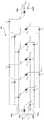
一个或多个实施例因此可以涉及如图4中例示的电压倍增器电路40。图4是具有用于生成正电压的单个分支架构的电压倍增器电路40的示例性电路图。One or more embodiments may thus involve a
如图4中所例示的,电压倍增器电路40包括在输入节点40a和输出节点40b之间布置的二极管D1,…,DN+1的链,基本上如参考图1和图2所讨论的,输入节点40a被配置为从电压源42接收输入电压VIN,输出节点40b被配置为产生输出电压VOUT。二极管链在输入节点40a和输出节点40b之间提供中间电压节点A1,...,AN的有序序列(例如,通用节点Ax对应于通用二极管Dx的阴极端子)。As illustrated in FIG. 4, the
电压倍增器电路40包括被配置为接收第一驱动时钟信号vCK的第一驱动输入节点44a和被配置为接收与第一驱动时钟信号vCK反相的第二驱动时钟信号
第一泵浦电容器组包括M个泵浦电容器CP,其第一端子被耦合到从1至2M编号(即,A1,…,A2M)的2M个中间电压节点的第一子序列中的奇数中间电压节点A1,A3,…,A2M-1(例如,第一节点和第三节点),并且其第二端子被耦合到第一驱动输入节点44a来接收第一驱动时钟信号vCK。第二泵浦电容器组包括M个泵浦电容器CP,其第一端子被耦合到2M个中间电压节点的第一子序列中的偶数中间电压节点A2,A4,…,A2M(例如,第二节点和第四节点),并且第二端子被耦合到第二驱动输入节点44b来接收第二驱动时钟信号
第三泵浦电容器组包括M个泵浦电容器CP,其第一端子被耦合到从2M+1至4M编号(图4中不可见)的2M个中间电压节点的第二子序列中的奇数中间电压节点A2M+1,A2M+3,…,A4M-1(例如,第一节点和第三节点),并且第二端子被耦合到从1至2M编号的2M个中间电压节点的第一子序列中的对应奇数中间电压节点A1,A3,…,A2M-1(例如,第一节点和第三节点)。换言之,第三组的泵浦电容器与第一组的泵浦电容器堆叠在一起,类似于Cockcroft-Walton架构。第四泵浦电容器组包括M个泵浦电容器CP,其第一端子被耦合到从2M+1至4M编号(图4中不可见)的2M个中间电压节点的第二子序列中的偶数中间电压节点A2M+2,A2M+4,…,A4M(例如,第二节点和第四节点),并且第二端子被耦合到从1至2M编号的2M个中间电压节点的第一子序列中的对应奇数中间电压节点A2,A4,…,A2M(例如,第二节点和第四节点)。换言之,第四组的泵浦电容器与第二组的泵浦电容器堆叠在一起,类似于Cockcroft-Walton架构。The third pump capacitor bank comprises M pump capacitors CP , the first terminals of which are coupled to an odd number in a second subsequence of 2M intermediate voltage nodes numbered from 2M+1 to 4M (not visible in FIG. 4 ). intermediate voltage nodes A2M+1 , A2M+3 , . Corresponding odd-numbered intermediate voltage nodes A1 , A3 , . . . , A2M-1 (eg, the first node and the third node) in the first subsequence. In other words, the pumping capacitors of the third bank are stacked with the pumping capacitors of the first bank, similar to the Cockcroft-Walton architecture. The fourth pump capacitor bank comprises M pump capacitors CP whose first terminals are coupled to even numbers in a second subsequence of 2M intermediate voltage nodes numbered from 2M+1 to 4M (not visible in FIG. 4 ). The intermediate voltage nodes A2M+2 , A2M+4 , . Corresponding odd-numbered intermediate voltage nodes A2 , A4 , . . . , A2M (eg, the second node and the fourth node) in the subsequence. In other words, the pumping capacitors of the fourth bank are stacked with the pumping capacitors of the second bank, similar to the Cockcroft-Walton architecture.
在本说明书中,当两个不同子序列的两个中间电压节点在相应有序子序列中占据相同位置(例如,第1位置、第2位置等)时,它们被称为“对应”。In this specification, two intermediate voltage nodes of two different subsequences are said to "correspond" when they occupy the same position (eg, 1st position, 2nd position, etc.) in the corresponding ordered subsequence.
泵浦电容器组的数目与电压倍增器的级数N和每组中电容器的数目M相关。一般而言,倒数第二泵浦电容器组包括M个泵浦电容器CP,其第一端子被耦合至从N-2M+1至N编号的2M个中间电压节点的最后子序列中的奇数中间电压节点AN-2M+1,AN-2M+3,…,AN-1,并且第二端子被耦合到从N-4M+1至N-2M编号(图4中不可见)的中间电压节点的倒数第二子序列中的对应奇数中间电压节点AN-4M+1,AN-4M+3,…,AN-2M-1。换言之,倒数第二组的泵浦电容器与倒数第四组的泵浦电容器堆叠在一起,类似于Cockcroft-Walton架构。最后一个泵浦电容器组包括M个泵浦电容器CP,其第一端子被耦合到从N-2M+1至N编号的2M个中间电压节点的最后子序列中的偶数中间电压节点AN-2M+2,AN-2M+4,…,AN,并且第二端子被耦合到从N-4M+1至N-2M编号(图4中不可见)的中间电压节点的倒数第二子序列中的对应偶数中间电压节点AN-4M+2,AN-4M+4,…,AN-2M。换言之,最后一组的泵浦电容器与倒数第三组的泵浦电容器堆叠在一起,类似于Cockcroft-Walton架构。The number of pump capacitor banks is related to the number N of voltage multiplier stages and the number M of capacitors in each bank. In general, the penultimate pump capacitor bank consists of M pump capacitors CP , the first terminals of which are coupled to the odd middle Voltage nodes AN-2M+1 , AN-2M+3 , ..., AN-1 , and second terminals are coupled to the middle of the nodes numbered from N-
因此,在如图4所例示的电压倍增器电路40中,前两组泵浦电容器CP基本上按照Dickson架构布置,而其余(中间和最后)组泵浦电容器CP堆叠到先前那些泵浦电容器,类似于Cockcroft-Walton倍增器(例如,它们的较低端子连接到前两组电容器中电容器的较高端子,较高端子连接到二极管链,逐渐朝向输出)。简而言之,属于同一组的泵浦电容器类似于Dickson电荷泵“并联”布置,而不同泵浦电容器组彼此堆叠,类似于Cockcroft-Walton电荷泵。Thus, in the
参考图5和图6解释图4中例示的电压倍增器电路40的操作。图5是在特别是当vCK=0(低值)和


在前半个时钟周期中,当vCK为低且


在由信号vCK驱动的第一组M个泵浦电容器中,第一泵浦电容器(耦合在节点44a和节点A1之间)以VIN-VD充电,第三泵浦电容器(耦合在节点44a和节点A3之间)以VIN+2VCK-3VD充电,第五泵浦电容器(耦合在节点44a和节点A5之间)以VIN+4VCK-5VD充电,依此类推,直到第(2M-1)泵浦电容器(耦合在节点44a和节点A2M-1之间)以VIN+(2M-2)·VCK-(2M-1)·VD充电。在由
注意,电压倍增器电路40的等效输出电阻可以根据以下等式(6)被计算为2M级Dickson倍增器和N/2M级Cockcroft-Walton倍增器的组合,假设时钟周期比时间常数RDCP长得多,其中RD是二极管电阻:Note that the equivalent output resistance of the

关于硅尺寸,比较用于计算ROUT的等式(3)和(6),注意,如图4中的架构(以下也称为“混合”架构)的尺寸可以被表示为:With respect to silicon size, compare Equations (3) and (6) for calculating ROUT , noting that the size of the architecture in Figure 4 (hereinafter also referred to as “hybrid” architecture) can be expressed as:

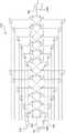
一个或多个实施例可以涉及如图7中例示的电压倍增器电路70。图7是基于参考图4、图5和图6所讨论的相同概念,具有用于生成正电压的双分支架构的电压倍增器电路70的示例性电路图。One or more embodiments may involve a
如图7所示,电压倍增器电路70包括:在输入节点40a和输出节点40b之间布置的N+1个二极管的第一链,输入节点40a和输出节点40b限定基本上如参考图4所讨论的中间节点A1,…,AN;以及在输入节点40a和输出节点40b之间布置的N+1个二极管的第二链,同样基本上如参考图4所讨论的,输入节点40a和输出节点40b限定中间电压节点B1,...,BN的另一集合。电压倍增器电路70包括2N个泵浦(或耦合)电容器CP/2。如图7所示,2N个泵浦电容器CP/2被布置在两个子集中,每个子集包括数目K=N/M的组(例如,集群),每个组包括M个电容器。第一子集包括由时钟信号vCK驱动(例如,耦合到节点44a)的泵浦电容器,而第二子集包括由时钟信号
泵浦电容器的第一子集的第一组包括泵浦电容器CP/2,其第一端子被耦合到第一电压节点集合A1,…,AN中从1至M编号的M个中间电压节点的第一子序列中的奇数中间电压节点A1,A3,…,AM-1(例如,第一节点和第三节点),并且第二端子被耦合到第一驱动输入节点44a来接收第一驱动时钟信号vCK。泵浦电容器的第一子集的第一组还包括泵浦电容器CP/2,其第一端子被耦合到第二电压节点集合B1,…,BN中从1至M编号的M个中间电压节点的第一子序列中的偶数中间电压节点B2,B4,…,BM(例如,第二节点和第四节点),并且第二端子被耦合到第一驱动输入节点44a来接收第一驱动时钟信号vCK。The first group of the first subset of pumping capacitors comprises pumping capacitors CP /2 whose first terminals are coupled to M middle ones numbered from 1 to M of the first set of voltage nodes A1 , . . . , AN Odd- numbered intermediate voltage nodes A1 , A3 , . to receive the first driving clock signal vCK . The first set of the first subset of pumping capacitors also includes pumping capacitors CP /2 whose first terminals are coupled to M of the second set of voltage nodes B1 ,...,BN numbered from 1 to M Even intermediate voltage nodes B2 ,B4 , . Receive the first driving clock signal vCK .
泵浦电容器的第二子集的第一组包括泵浦电容器CP/2,其第一端子被耦合到第一电压节点集合A1,…,AN中从1至M编号的M个中间电压节点的第一子序列中的偶数中间电压节点A2,A4,…,AM(例如,第二节点和第四节点),并且第二端子被耦合到第二驱动输入节点44b来接收第二驱动时钟信号

泵浦电容器的第一子集的第二组包括泵浦电容器CP/2,其第一端子被耦合到第一电压节点集合A1,…,AN中从M+1至2M编号的M个中间电压节点的第二子序列中的奇数中间电压节点AM+1,AM+3,…,A2M-1(例如,第一节点和第三节点),并且第二端子被耦合到第一电压节点集合A1,…,AN中从1至M编号的M个中间电压节点的第一子序列中的对应奇数中间电压节点A1,A3,…,AM-1(例如,第一节点和第三节点)。泵浦电容器的第二子集的第二组还包括泵浦电容器CP/2,其第一端子被耦合到第二电压节点集合B1,…,BN中从M+1至2M编号的M个中间电压节点的第二子序列中的偶数中间电压节点BM+2,BM+4,…,B2M(例如,第二节点和第四节点),并且第二端子被耦合到第二电压节点集合B1,…,BN中从1至M编号的M个中间电压节点的第一子序列中的对应偶数中间电压节点B2,B4,…,BM(例如,第二节点和第四节点)。The second set of the first subset of pumping capacitors includes pumping capacitors CP /2 whose first terminals are coupled to M of the first set of voltage nodes A1 ,..., AN numbered from M+1 to 2M Odd-numbered intermediate voltage nodes AM+1 , AM+3 , ..., A2M-1 (for example, the first node and the third node) in the second subsequence of intermediate voltage nodes, and the second terminal is coupled to Corresponding odd-numbered intermediate voltage nodes A1 , A3 ,..., AM-1 in the first subsequence of M intermediate voltage nodes numbered from 1 to M in the first voltage node set A1 ,...,AN (for example , the first node and the third node). The second set of the second subset of pumping capacitors also includes pumping capacitors CP /2 whose first terminals are coupled to the second set of voltage nodes B1 ,...,BN numbered from M+1 to 2M The even-numbered intermediate voltage nodes BM+2 , BM+4 , ..., B2M (for example, the second node and the fourth node) in the second subsequence of M intermediate voltage nodes, and the second terminal is coupled to the second node Corresponding even-numbered intermediate voltage nodes B2 , B4 ,..., BM in the first subsequence of M intermediate voltage nodes numbered from 1 to M in the two-voltage node set B1 ,...,BN (for example, the second node and the fourth node).
泵浦电容器的第二子集的第二组包括泵浦电容器CP/2,其第一端子被耦合到第一电压节点集合A1,…,AN中从M+1至2M编号的M个中间电压节点的第二子序列中的偶数中间电压节点AM+2,AM+4,…,A2M(例如,第二节点和第四节点),并且第二端子被耦合到第一电压节点集合A1,…,AN中从1至M编号的M个中间电压节点的第一子序列中的对应偶数中间电压节点A2,A4,…,AM(例如,第二节点和第四节点)。泵浦电容器的第二子集的第二组还包括泵浦电容器CP/2,其第一端子被耦合到第二电压节点集合B1,…,BN中从M+1至2M编号的M个中间电压节点的第二子序列中的奇数中间电压节点BM+1,BM+3,…,B2M-1(例如,第一节点和第三节点),并且第二端子被耦合到第二电压节点集合B1,…,BN中从1至M编号的M个中间电压节点的第一子序列中的对应奇数中间电压节点B1,B3,…,BM-1(例如,第一节点和第三节点)。The second group of the second subset of pumping capacitors comprises pumping capacitors CP /2 whose first terminals are coupled to M of the first set of voltage nodes A1 ,..., AN numbered from M+1 to 2M The even-numbered intermediate voltage nodes AM+2 , AM+4 , ..., A2M (for example, the second node and the fourth node) in the second subsequence of intermediate voltage nodes, and the second terminal is coupled to the first Corresponding even-numbered intermediate voltage nodes A2 ,A 4, ..., AM( for example, the second node and fourth node). The second set of the second subset of pumping capacitors also includes pumping capacitors CP /2 whose first terminals are coupled to the second set of voltage nodes B1 ,...,BN numbered from M+1 to 2M Odd-numbered intermediate voltage nodes BM+1 , BM+3 , ..., B2M-1 (for example, the first node and the third node) in the second subsequence of M intermediate voltage nodes, and the second terminal is coupled To the corresponding odd-numbered intermediate voltage nodes B1 , B3 ,..., BM-1( For example, first node and third node).
通常,泵浦电容器的第一子集的最后一组包括泵浦电容器CP/2,其第一端子被耦合到第一电压节点集合A1,…,AN中从N-M+1至N编号的M个中间电压节点的最后子序列中的奇数中间电压节点AN-M+1,AN-M+3,…,AN-1(例如,第一节点和第三节点),并且第二端子被耦合到第一电压节点集合A1,…,AN中从N-2M+1至N-M编号的M个中间电压节点的倒数第二子序列中的对应奇数中间电压节点AN-2M+1,AN-2M+3,…,AN-M-1(例如,第一节点和第三节点)。泵浦电容器的第一子集的最后一组还包括泵浦电容器CP/2,其第一端子被耦合到第二电压节点集合B1,…,BN中从N-M+1至N编号的M个中间电压节点的最后子序列中的偶数中间电压节点BN-M+2,BN-M+4,…,BN(例如,第二节点和第四节点),并且第二端子被耦合到第二电压节点集合B1,…,BN中从N-2M+1至N-M编号的M个中间电压节点的倒数第二子序列中的对应偶数中间电压节点BN-2M+2,BN-2M+4,…,BN-M(例如,第二节点和第四节点)。Typically, the last set of the first subset of pumping capacitors comprises pumping capacitors CP /2 whose first terminals are coupled to a first set of voltage nodes A1 ,..., AN from N-M+1 to Odd-numbered intermediate voltage nodesAN-M+1 ,AN-M+3 ,...,AN-1 (for example, the first node and the third node) in the last subsequence of N numbered M intermediate voltage nodes, And the second terminal is coupled to the corresponding odd-numbered intermediate voltage node AN in the penultimate subsequence of M intermediate voltage nodes numbered fromN -
通常,泵浦电容器的第二子集的最后一组包括泵浦电容器CP/2,其第一端子被耦合到第一电压节点集合A1,…,AN中从N-M+1至N编号的M个中间电压节点的最后子序列中的偶数中间电压节点AN-M+2,AN-M+4,…,AN(例如,第二节点和第四节点),并且第二端子被耦合到第一电压节点集合A1,…,AN中从N-2M+1至N-M编号的M个中间电压节点的倒数第二子序列中的对应偶数中间电压节点AN-2M+2,AN-2M+4,…,AN-M(例如,第二节点和第四节点)。泵浦电容器的第二子集的最后一组还包括泵浦电容器CP/2,其第一端子被耦合到第二电压节点集合B1,…,BN中从N-M+1至N编号的M个中间电压节点的最后子序列中的奇数中间电压节点BN-M+1,BN-M+3,…,BN-1(例如,第一节点和第三节点),并且第二端子被耦合到第二电压节点集合B1,…,BN中从N-2M+1至N-M编号的M个中间电压节点的倒数第二子序列中的对应奇数中间电压节点BN-2M+1,BN-2M+3,…,BN-M-1(例如,第一节点和第三节点)。Typically, the last set of the second subset of pumping capacitors comprises pumping capacitors CP /2 whose first terminals are coupled to the first set of voltage nodes A1 ,..., AN from N-M+1 to Even-numbered intermediate voltage nodes AN-M+2 , AN-M+4 ,..., AN (for example, the second node and the fourth node) in the last subsequence of N numbered M intermediate voltage nodes, and the The two terminals are coupled to the corresponding even-numbered intermediate voltage node AN-2M in the penultimate subsequence of the M intermediate voltage nodes numbered from N-
注意,虽然图7的架构已具体参考每个子集中的第一组、第二组和最后一组泵浦电容器进行了描述,但泵浦电容器组的数目(即,数目K=N/M)可以根据设计规范而变化,每个组“堆叠”到前一组上(例如,参见图7中与节点Ai+1,Bi+2,Ai+3,Bi+M和Bi+1,Ai+2,Bi+3,Ai+M耦合的中间电容器组)。Note that while the architecture of FIG. 7 has been described with specific reference to the first, second, and last sets of pump capacitors in each subset, the number of pump capacitor banks (i.e., number K=N/M) may Depending on the design specification, each group "stacks" on top of the previous group (see, for example, Figure 7 with nodes Ai+1 , Bi+2 , Ai+3 , Bi+M and Bi+1 , Ai+2 , Bi+3 , Ai+M coupled middle capacitor bank).
如果每个泵浦电容器CP/2的电容值是单分支架构的泵浦电容器CP的电容值的一半,则电压倍增器电路70的开路负载电压VO与等式(2)中报告的相同。单分支和双分支架构之间的电容总量没有变化,双分支架构包括2N*CP/2个电容器,而单分支架构包括N*CP个电容器。就倍增器输出上的电压纹波以及电容器和二极管中的电流峰值而言,图7中例示的双分支架构可能是有利的,相对于单分支架构减半。If the capacitance value of each pumping capacitor CP /2 is half that of the pumping capacitor CP of the single-branch architecture, the open-circuit load voltage VO of the
双分支电压倍增器70的操作类似于单分支架构的操作,其中跨泵浦电容器的电压减半,因为图7的架构对称并且对于给定的N级倍增器,泵浦电容器的数目是双倍的。The operation of the two-
在第一子集的第一泵浦电容器组中(直接连接到节点44a并且由信号vCK驱动)以及在第二子集的第一泵浦电容器组中(直接连接到节点44b并且由信号
注意,电压倍增器电路70的等效输出电阻可以根据以下等式(8)被计算为M级Dickson倍增器和N/M级Cockcroft-Walton倍增器的组合,假设时钟周期比时间常数RDCP长得多,其中RD是二极管电阻:Note that the equivalent output resistance of the

关于硅尺寸,比较用于计算ROUT的等式(3)和(8),注意,如图7中的架构(以下也称为“混合双”架构)的尺寸可以被表示为:With respect to silicon size, compare Equations (3) and (8) for computing ROUT , noting that the size of the architecture in Figure 7 (also referred to below as a “hybrid dual” architecture) can be expressed as:

在一个或多个实施例中(例如,在片上实现方式中),二极管D1,…,DN+1可以由图8中例示的MOS晶体管代替。应当注意,图8的电压倍增器电路80基本上对应于图4的架构,其中二极管D1,…,DN+1被MOS晶体管M1,…,MN+1替换。MOS晶体管可以是n沟道和/或p沟道,只要它们根据时钟信号vCK和
参考图9和图10解释图8中例示的电压倍增器电路80的操作。图9是在特别是当vCK=0(低值)且


在前半个时钟周期中,当vCK为低且


在直接连接到节点44a并由信号vCK驱动的第一泵浦电容器组中,第一泵浦电容器(耦合在节点44a和节点A1之间)以VIN充电,第三泵浦电容器(耦合在节点44a和节点A3之间)以VIN+2VCK充电,第五泵浦电容器(耦合在节点44a和节点A5之间)以VIN+4VCK充电,依此类推,直到第(2M-1)泵浦电容器(耦合在节点44a和节点A5之间)以VIN+(2M-2)·VCK充电。在直接连接到节点44b并由信号
VO=VIN+N·VCK (10)VO =VIN +N·VCK (10)
注意,如图8所示的电压倍增器电路80的等效输出电阻与等式(6)中定义的相同,假设时钟周期比时间常数RMCP长得多,其中RM是MOS晶体管电阻。Note that the equivalent output resistance of the
在一个或多个实施例中,如图11中所例示的,MOS晶体管也可以被用于在双分支架构中替换二极管。应注意,图11的电压倍增器电路110基本上对应于图7的架构,其中使用MOS晶体管替换二极管。MOS晶体管可以是n沟道和/或p沟道,只要它们被适当地驱动(例如,根据参考图9和图10讨论的驱动方案,如果正输出电压被生成)。In one or more embodiments, as illustrated in FIG. 11 , MOS transistors may also be used to replace diodes in a two-branch architecture. It should be noted that the
注意,如图11中例示的电压倍增器电路110的等效输出电阻与等式(8)中定义的相同,假设时钟周期远长于时间常数RMCP,其中RM为MOS晶体管电阻。此外,如图11中例示的电压倍增器电路110的开路负载电压VO与等式(10)中定义的相同。就倍增器输出上的电压纹波以及电容器和MOS晶体管中的电流峰值而言,如图11中例示的双分支MOS架构可能是有利的,相对于单分支MOS架构减半。Note that the equivalent output resistance of the
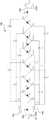
通常,用于生成正电压的双分支电压倍增器电路可以被实现为如图12的电路图所示。Generally, a two-branch voltage multiplier circuit for generating positive voltages can be implemented as shown in the circuit diagram of FIG. 12 .
如图12中所例示的,电压倍增器电路120包括在输入节点40a和输出节点40b之间布置的N个电荷转移电路块130的链。如图13所示,每个电荷转移电路块130具有输入端子Vd、输出端子Vu、第一控制端子和第二控制端子。电荷转移电路块130包括电子组件(例如,二极管和/或晶体管),电子组件被布置为使得当两个反相的切换信号被施加到第一和第二控制端子时,电荷从输入端子Vd转移到输出端子Vu。具体地,根据在两个控制端子处接收的控制信号的值,电路块130可以在两种不同的换向状态下操作:在第一状态中,输入端子Vd被耦合到第一控制端子并且输出端子Vu被耦合到第二控制端子;在第二状态下,输入端子Vd被耦合到第二控制端子,并且输出端子Vu被耦合到第一控制端子。As illustrated in FIG. 12, the
如图12中所例示的,每个电荷转移电路块130的第一控制端子和第二控制端子被配置为经由相应的泵浦电容器CP/2接收互补控制信号(例如,vCK和
在块130的第一子链中,每个块130的第一控制端子经由相应的泵浦电容器CP/2耦合到第一驱动输入节点44a,并且每个块130的第二控制端子经由相应的泵浦电容器CP/2被耦合到第二驱动输入节点44b。在块130的第二子链中,每个块130的第一控制端子经由相应的泵浦电容器CP/2而被耦合到第一子链中对应块130的第一控制端子,并且每个块130的第二控制端子经由相应的泵浦电容器CP/2而被耦合到第一子链中对应块130的第二控制端子。换言之,与第二子链中的块130耦合的泵浦电容器被堆叠至与第一子链中的块130耦合的泵浦电容器。In the first sub-chain of
子链的数目K与级数N和每个子链中的块的数目M相关。通常,在块130的第j子链中,每个块130的第一控制端子经由相应的泵浦电容器CP/2而被耦合到第(j-1)子链中对应块130的第一控制端子,并且每个块130的第二控制端子经由相应的泵浦电容器CP/2而被耦合到第(j-1)子链中对应块130的第二控制端子。The number K of sub-chains is related to the number of stages N and the number M of blocks in each sub-chain. Typically, in the jth subchain of
例如,在一个或多个实施例中,每个电荷转移电路块130可以包括如图14中例示的布置。布置包括:第一n沟道晶体管Nl,其具有在输入端子Vd和第一控制端子之间的电流路径;第二n沟道晶体管N2,其具有在输入端子Vd和第二控制端子之间的电流路径;第一p沟道晶体管P1,其具有在输出端子Vu和第一控制端子之间的电流路径;以及第二p沟道晶体管P2,其具有在输出端子Vu和第二控制端子之间的电流路径。第一n沟道晶体管N1和第一p沟道晶体管P1的栅极端子被耦合到第二控制端子,并且第二n沟道晶体管N2和第二p沟道晶体管P2的栅极端子被耦合到第一控制端子。For example, in one or more embodiments, each charge
在文献[Pulvirenti]和[Gariboldi 96]中公开了在锁存电荷泵中使用的这样的布置的操作,并且因此为了简洁起见,在此不再重复。The operation of such an arrangement used in latching charge pumps is disclosed in documents [Pulvirenti] and [Gariboldi 96] and is therefore not repeated here for the sake of brevity.
一个或多个实施例可以被用于生成负电压。如图17的电路图所示,这可以例如通过如图15和图16的电路图中分别例示的反转图4和图7架构中的二极管的极性来获得,或者反转图8和图11的架构中的MOS晶体管的激活信号的极性来获得,或者反转(例如,翻转)图12的架构中的电荷转移电路块130的方向(例如,交换端子Vu和Vd)来获得。One or more embodiments may be used to generate negative voltages. This can be obtained, for example, by reversing the polarity of the diodes in the architectures of FIGS. 4 and 7, as illustrated in the circuit diagrams of FIGS. 15 and 16, respectively, or by reversing the The polarity of the activation signal of the MOS transistor in the architecture is obtained, or the direction of the charge
图15中例示的单分支负电压倍增器电路150的操作类似于图4中例示的单分支正电压倍增器电路40的操作,因此以下仅通过示例方式进行讨论。在前半个时钟周期中,当vCK为低且


第一泵浦电容器(耦合在节点44a和节点A1之间)以VIN-VCK+VD充电,第二泵浦电容器(耦合在节点44b和节点A2之间)以VIN-2VCK+2VD充电,第三泵浦电容器(耦合在节点44a和节点A3之间)以VIN-3VCK+3VD充电,依此类推。在单分支架构中,从2M到N的泵浦电容均以-2M·(VCK-VD)充电;在双分支架构中,从M到N的泵浦电容器均以-M·(VCK-VD)充电。开路负载输出电压VO在以下的等式(11)中报告:Thefirst pump capacitor (coupled between
VO=VIN-N·VCK+(N+1)·VD (11)VO =VIN -N·VCK +(N+1)·VD (11)
注意,电压倍增器电路150的等效输出电阻与等式(6)中报告的相同。Note that the equivalent output resistance of the
还应注意,将第一二极管连接到接地而不是连接到VIN,输出电压变得更负。Note also that by connecting the first diode to ground instead of VIN , the output voltage becomes more negative.
如图16中例示的双分支负电压倍增器160的操作类似于单分支负架构的操作,其中跨泵浦电容器的电压减半,并且为了简洁,本文中将不再描述。The operation of the dual-branch
如图8中例示的基于MOS晶体管架构的负电压倍增器电路的操作可以通过反转先前参考图9和图10解释的操作来获得,即,反转MOS晶体管相对于时钟信号的两个半周期的激活阶段。在这种情况下,在前半个时钟周期中,当vCK为低且


第一泵浦电容器(耦合在节点44a和节点A1之间)以VIN-VCK充电,第二泵浦电容器(耦合在节点44b和节点A2之间)以VIN-2VCK下充电,第三泵浦电容器(耦合在节点44a和节点A3之间)以VIN-3VCK下充电,依此类推。在单分支架构中,从2M到N的泵浦电容均以-2M·VCK充电;在双分支架构中,从M到N的泵浦电容器均以-M·VCK下充电。开路负载输出电压VO在以下等式(12)中报告:Thefirst pump capacitor (coupled between
VO=VIN-N·VCK (12)VO =VIN -N·VCK (12)
等效输出电阻与等式(6)中定义的相同。The equivalent output resistance is the same as defined in equation (6).
具有MOS晶体管的双分支负电压倍增器的操作与单分支的操作类似,因此为简洁起见不再进一步描述。The operation of the dual-branch negative voltage multiplier with MOS transistors is similar to that of the single-branch and thus will not be described further for brevity.
在描述末尾处提供的表I和II总结了本文讨论的电压倍增器电路的开路负载电压VO、输出电阻ROUT和总电容量CTOT的公式。Tables I and II provided at the end of the description summarize the formulas for the open-circuit load voltage VO , the output resistance ROUT and the total capacitance CTOT for the voltage doubler circuits discussed herein.
一个或多个实施例可以仅作为示例应用于针对MEMS(微机电系统)开关的单片八进制驱动器,其中驱动器的供电轨VOUT=70V从电源VDD=3.3V开始生成。例如,一个或多个实施例可以使用诸如SOI-BCD6s技术的绝缘体上硅(SOI)技术和具有12V操作电压的泵浦电容器来实现。考虑到3.0V的稳压电源,这样的示例性倍增器可以具有几乎N=24个级。此外,假设VIN=VCK=3.0V,M可以被选择来将泵浦电容器的操作电压(例如,12V)除以稳压电源(例如,3.0V)。到目前为止,M可以等于4,因为泵浦电容器上的最大电压不会超过12V的操作值。根据等式(9),当M=1时,24个N级Cockcroft-Walton倍增器将比Dickson大204倍,而根据M=4的等式(9),根据一个或多个实施例的具有24个N级和4个M级的倍增器将比Dickson大15.2倍并且比Cockcroft-Walton小13.4倍。One or more embodiments may be applied by way of example only to a monolithic octal driver for MEMS (Micro-Electro-Mechanical System) switches, where the driver's supply rail VOUT =70V is generated from a supply VDD =3.3V. For example, one or more embodiments may be implemented using silicon-on-insulator (SOI) technology such as SOI-BCD6s technology and a pump capacitor with a 12V operating voltage. Considering a regulated supply of 3.0V, such an exemplary multiplier may have almost N=24 stages. Furthermore, assuming VIN =VCK =3.0V, M can be chosen to divide the operating voltage of the pump capacitor (eg, 12V) by the regulated power supply (eg, 3.0V). So far, M can be equal to 4, because the maximum voltage on the pump capacitor will not exceed the operating value of 12V. According to equation (9), when M = 1, 24 N-stage Cockcroft-Walton multipliers will be 204 times larger than Dickson, while according to equation (9) with M = 4, according to one or more embodiments with A multiplier of 24 N-levels and 4 M-levels would be 15.2 times larger than Dickson and 13.4 times smaller than Cockcroft-Walton.
一个或多个实施例因此可以提供具有减小的硅面积占用的集成电压倍增器电路。One or more embodiments may thus provide an integrated voltage multiplier circuit with a reduced silicon area footprint.
在不损害基本原理的情况下,在不脱离保护范围的情况下,细节和实施例可以相对于仅以示例方式描述的内容变化甚至显著变化。The details and embodiments may vary, even significantly, from what has been described by way of example only, without prejudice to the underlying principles, and without departing from the scope of protection.
保护范围由所附权利要求确定。The scope of protection is determined by the appended claims.
表1Table 1
表2Table 2

Claims (20)
Applications Claiming Priority (4)
| Application Number | Priority Date | Filing Date | Title |
|---|---|---|---|
| IT202100012167 | 2021-05-12 | ||
| IT102021000012167 | 2021-05-12 | ||
| US17/732,281 | 2022-04-28 | ||
| US17/732,281US11929674B2 (en) | 2021-05-12 | 2022-04-28 | Voltage multiplier circuit |
Publications (1)
| Publication Number | Publication Date |
|---|---|
| CN115347782Atrue CN115347782A (en) | 2022-11-15 |
Family
ID=83949042
Family Applications (1)
| Application Number | Title | Priority Date | Filing Date |
|---|---|---|---|
| CN202210517047.XAPendingCN115347782A (en) | 2021-05-12 | 2022-05-11 | Voltage multiplier circuit |
Country Status (2)
| Country | Link |
|---|---|
| US (1) | US12368376B2 (en) |
| CN (1) | CN115347782A (en) |
Families Citing this family (2)
| Publication number | Priority date | Publication date | Assignee | Title |
|---|---|---|---|---|
| JP7519442B2 (en)* | 2020-07-22 | 2024-07-19 | 株式会社日立ハイテク | DC high voltage power supply and charged particle beam device |
| KR102607469B1 (en)* | 2022-11-30 | 2023-11-29 | 덕산네오룩스 주식회사 | Method for preparing pixel define layer |
Citations (5)
| Publication number | Priority date | Publication date | Assignee | Title |
|---|---|---|---|---|
| EP1199788A1 (en)* | 2000-10-17 | 2002-04-24 | STMicroelectronics S.r.l. | Inductive DC-to-DC switching converter |
| CN101669026A (en)* | 2006-12-14 | 2010-03-10 | 离子流系统有限公司 | Utilize the method and apparatus of large-scale F ET array measurement analyte |
| CN104871108A (en)* | 2012-11-26 | 2015-08-26 | 北极砂技术有限公司 | Pump capacitor configuration for switched capacitor circuits |
| CN110352559A (en)* | 2017-03-03 | 2019-10-18 | 株式会社半导体能源研究所 | Semiconductor device and driving method of semiconductor device |
| US20190393776A1 (en)* | 2018-06-25 | 2019-12-26 | Psemi Corporation | Start-up of step-up power converter with switched-capacitor network |
Family Cites Families (11)
| Publication number | Priority date | Publication date | Assignee | Title |
|---|---|---|---|---|
| CH553481A (en) | 1972-06-27 | 1974-08-30 | Battelle Memorial Institute | SET TO POLARIZE THE SUBSTRATE OF AN INTEGRATED CIRCUIT. |
| EP0696839B1 (en) | 1994-08-12 | 1998-02-25 | Co.Ri.M.Me. Consorzio Per La Ricerca Sulla Microelettronica Nel Mezzogiorno | Voltage elevator of the charge pump type |
| US20030184360A1 (en) | 2002-03-29 | 2003-10-02 | Yi-Ti Wang | Charge pump for flash memory with serially connected capacitors for preventing breakdown |
| TWI233617B (en)* | 2004-01-02 | 2005-06-01 | Univ Nat Chiao Tung | Charge pump circuit suitable for low voltage process |
| US7239194B2 (en)* | 2004-03-25 | 2007-07-03 | Integral Wave Technologies, Inc. | Trench capacitor power supply system and method |
| US7855591B2 (en) | 2006-06-07 | 2010-12-21 | Atmel Corporation | Method and system for providing a charge pump very low voltage applications |
| US9203299B2 (en)* | 2013-03-15 | 2015-12-01 | Artic Sand Technologies, Inc. | Controller-driven reconfiguration of switched-capacitor power converter |
| EP3355459B1 (en) | 2017-01-30 | 2020-01-29 | ams AG | Voltage converter and method for voltage conversion |
| US10461635B1 (en)* | 2018-05-15 | 2019-10-29 | Analog Devices Global Unlimited Company | Low VIN high efficiency chargepump |
| US11589447B2 (en)* | 2021-04-07 | 2023-02-21 | Energy Resources International Co., Ltd. | Driving device for driving a high-voltage X ray tube and method thereof driving the same |
| US11929674B2 (en) | 2021-05-12 | 2024-03-12 | Stmicroelectronics S.R.L. | Voltage multiplier circuit |
- 2022
- 2022-05-11CNCN202210517047.XApatent/CN115347782A/enactivePending
- 2024
- 2024-02-05USUS18/432,576patent/US12368376B2/enactiveActive
Patent Citations (5)
| Publication number | Priority date | Publication date | Assignee | Title |
|---|---|---|---|---|
| EP1199788A1 (en)* | 2000-10-17 | 2002-04-24 | STMicroelectronics S.r.l. | Inductive DC-to-DC switching converter |
| CN101669026A (en)* | 2006-12-14 | 2010-03-10 | 离子流系统有限公司 | Utilize the method and apparatus of large-scale F ET array measurement analyte |
| CN104871108A (en)* | 2012-11-26 | 2015-08-26 | 北极砂技术有限公司 | Pump capacitor configuration for switched capacitor circuits |
| CN110352559A (en)* | 2017-03-03 | 2019-10-18 | 株式会社半导体能源研究所 | Semiconductor device and driving method of semiconductor device |
| US20190393776A1 (en)* | 2018-06-25 | 2019-12-26 | Psemi Corporation | Start-up of step-up power converter with switched-capacitor network |
Also Published As
| Publication number | Publication date |
|---|---|
| US20240195294A1 (en) | 2024-06-13 |
| US12368376B2 (en) | 2025-07-22 |
Similar Documents
| Publication | Publication Date | Title |
|---|---|---|
| US11929674B2 (en) | Voltage multiplier circuit | |
| JP3488587B2 (en) | Boost circuit and IC card having the same | |
| CN103270682B (en) | Due to the charge pump system of the shared poor efficiency minimizing of the electric charge between electric capacity | |
| US8018270B2 (en) | Charge pump circuit | |
| US7605640B2 (en) | N-stage exponential charge pumps, charging stages therefor and methods of operation thereof | |
| US5748032A (en) | Charge pumping circuit for generating a high output voltage | |
| US7215179B2 (en) | Booster circuit | |
| US12368376B2 (en) | Voltage multiple circuit | |
| US7652522B2 (en) | High efficiency low cost bi-directional charge pump circuit for very low voltage applications | |
| US20070285150A1 (en) | Method and system for providing a charge pump very low voltage applications | |
| CN101373927A (en) | Charge pump circuit, method of operating the same, and semiconductor device | |
| CN101159412A (en) | Electronic device including boosting circuit | |
| JP2004274861A (en) | Boost circuit | |
| US6385065B1 (en) | Low voltage charge pump employing distributed charge boosting | |
| US7714636B2 (en) | Charge pump circuit and cell thereof | |
| US20090302930A1 (en) | Charge Pump with Vt Cancellation Through Parallel Structure | |
| CN1477773B (en) | Charge Pump Circuit Based on Coupling Capacitor Sharing | |
| KR100636508B1 (en) | Charge Pump Circuit and DC Converter Using the Same | |
| US6605985B2 (en) | High-efficiency power charge pump supplying high DC output currents | |
| JP2008253031A (en) | Charge pump circuit | |
| CN115622389A (en) | Charge Pump Circuitry and Memory | |
| TW466495B (en) | Charge pump circuit | |
| CN100481687C (en) | Voltage converter for converting an input voltage to an output voltage and driving circuit and method thereof | |
| Mohammad et al. | Switched positive/negative charge pump design using standard CMOS transistors | |
| US7095268B2 (en) | Single-stage and modular multi-stage clock-booster |
Legal Events
| Date | Code | Title | Description |
|---|---|---|---|
| PB01 | Publication | ||
| PB01 | Publication | ||
| SE01 | Entry into force of request for substantive examination | ||
| SE01 | Entry into force of request for substantive examination |