CN115346488A - Organic Light Emitting Display Devices - Google Patents
Organic Light Emitting Display DevicesDownload PDFInfo
- Publication number
- CN115346488A CN115346488ACN202211110273.2ACN202211110273ACN115346488ACN 115346488 ACN115346488 ACN 115346488ACN 202211110273 ACN202211110273 ACN 202211110273ACN 115346488 ACN115346488 ACN 115346488A
- Authority
- CN
- China
- Prior art keywords
- node
- transistor
- period
- coupled
- scan
- Prior art date
- Legal status (The legal status is an assumption and is not a legal conclusion. Google has not performed a legal analysis and makes no representation as to the accuracy of the status listed.)
- Granted
Links
- 239000003990capacitorSubstances0.000claimsabstractdescription75
- 241000820057IthoneSpecies0.000claims6
- 230000003247decreasing effectEffects0.000claims1
- 238000000034methodMethods0.000description28
- 239000010410layerSubstances0.000description13
- 238000010586diagramMethods0.000description10
- 230000008878couplingEffects0.000description8
- 238000010168coupling processMethods0.000description8
- 238000005859coupling reactionMethods0.000description8
- 230000007423decreaseEffects0.000description3
- 230000007274generation of a signal involved in cell-cell signalingEffects0.000description3
- 239000000758substrateSubstances0.000description2
- 238000003491arrayMethods0.000description1
- 230000015572biosynthetic processEffects0.000description1
- 239000004973liquid crystal related substanceSubstances0.000description1
- 239000012044organic layerSubstances0.000description1
- 230000001360synchronised effectEffects0.000description1
Images


Classifications
- G—PHYSICS
- G09—EDUCATION; CRYPTOGRAPHY; DISPLAY; ADVERTISING; SEALS
- G09G—ARRANGEMENTS OR CIRCUITS FOR CONTROL OF INDICATING DEVICES USING STATIC MEANS TO PRESENT VARIABLE INFORMATION
- G09G3/00—Control arrangements or circuits, of interest only in connection with visual indicators other than cathode-ray tubes
- G09G3/20—Control arrangements or circuits, of interest only in connection with visual indicators other than cathode-ray tubes for presentation of an assembly of a number of characters, e.g. a page, by composing the assembly by combination of individual elements arranged in a matrix no fixed position being assigned to or needed to be assigned to the individual characters or partial characters
- G09G3/22—Control arrangements or circuits, of interest only in connection with visual indicators other than cathode-ray tubes for presentation of an assembly of a number of characters, e.g. a page, by composing the assembly by combination of individual elements arranged in a matrix no fixed position being assigned to or needed to be assigned to the individual characters or partial characters using controlled light sources
- G09G3/30—Control arrangements or circuits, of interest only in connection with visual indicators other than cathode-ray tubes for presentation of an assembly of a number of characters, e.g. a page, by composing the assembly by combination of individual elements arranged in a matrix no fixed position being assigned to or needed to be assigned to the individual characters or partial characters using controlled light sources using electroluminescent panels
- G09G3/32—Control arrangements or circuits, of interest only in connection with visual indicators other than cathode-ray tubes for presentation of an assembly of a number of characters, e.g. a page, by composing the assembly by combination of individual elements arranged in a matrix no fixed position being assigned to or needed to be assigned to the individual characters or partial characters using controlled light sources using electroluminescent panels semiconductive, e.g. using light-emitting diodes [LED]
- G09G3/3208—Control arrangements or circuits, of interest only in connection with visual indicators other than cathode-ray tubes for presentation of an assembly of a number of characters, e.g. a page, by composing the assembly by combination of individual elements arranged in a matrix no fixed position being assigned to or needed to be assigned to the individual characters or partial characters using controlled light sources using electroluminescent panels semiconductive, e.g. using light-emitting diodes [LED] organic, e.g. using organic light-emitting diodes [OLED]
- G09G3/3266—Details of drivers for scan electrodes
- G—PHYSICS
- G09—EDUCATION; CRYPTOGRAPHY; DISPLAY; ADVERTISING; SEALS
- G09G—ARRANGEMENTS OR CIRCUITS FOR CONTROL OF INDICATING DEVICES USING STATIC MEANS TO PRESENT VARIABLE INFORMATION
- G09G3/00—Control arrangements or circuits, of interest only in connection with visual indicators other than cathode-ray tubes
- G09G3/20—Control arrangements or circuits, of interest only in connection with visual indicators other than cathode-ray tubes for presentation of an assembly of a number of characters, e.g. a page, by composing the assembly by combination of individual elements arranged in a matrix no fixed position being assigned to or needed to be assigned to the individual characters or partial characters
- G09G3/22—Control arrangements or circuits, of interest only in connection with visual indicators other than cathode-ray tubes for presentation of an assembly of a number of characters, e.g. a page, by composing the assembly by combination of individual elements arranged in a matrix no fixed position being assigned to or needed to be assigned to the individual characters or partial characters using controlled light sources
- G09G3/30—Control arrangements or circuits, of interest only in connection with visual indicators other than cathode-ray tubes for presentation of an assembly of a number of characters, e.g. a page, by composing the assembly by combination of individual elements arranged in a matrix no fixed position being assigned to or needed to be assigned to the individual characters or partial characters using controlled light sources using electroluminescent panels
- G09G3/32—Control arrangements or circuits, of interest only in connection with visual indicators other than cathode-ray tubes for presentation of an assembly of a number of characters, e.g. a page, by composing the assembly by combination of individual elements arranged in a matrix no fixed position being assigned to or needed to be assigned to the individual characters or partial characters using controlled light sources using electroluminescent panels semiconductive, e.g. using light-emitting diodes [LED]
- G09G3/3208—Control arrangements or circuits, of interest only in connection with visual indicators other than cathode-ray tubes for presentation of an assembly of a number of characters, e.g. a page, by composing the assembly by combination of individual elements arranged in a matrix no fixed position being assigned to or needed to be assigned to the individual characters or partial characters using controlled light sources using electroluminescent panels semiconductive, e.g. using light-emitting diodes [LED] organic, e.g. using organic light-emitting diodes [OLED]
- G09G3/3225—Control arrangements or circuits, of interest only in connection with visual indicators other than cathode-ray tubes for presentation of an assembly of a number of characters, e.g. a page, by composing the assembly by combination of individual elements arranged in a matrix no fixed position being assigned to or needed to be assigned to the individual characters or partial characters using controlled light sources using electroluminescent panels semiconductive, e.g. using light-emitting diodes [LED] organic, e.g. using organic light-emitting diodes [OLED] using an active matrix
- G09G3/3233—Control arrangements or circuits, of interest only in connection with visual indicators other than cathode-ray tubes for presentation of an assembly of a number of characters, e.g. a page, by composing the assembly by combination of individual elements arranged in a matrix no fixed position being assigned to or needed to be assigned to the individual characters or partial characters using controlled light sources using electroluminescent panels semiconductive, e.g. using light-emitting diodes [LED] organic, e.g. using organic light-emitting diodes [OLED] using an active matrix with pixel circuitry controlling the current through the light-emitting element
- G—PHYSICS
- G09—EDUCATION; CRYPTOGRAPHY; DISPLAY; ADVERTISING; SEALS
- G09G—ARRANGEMENTS OR CIRCUITS FOR CONTROL OF INDICATING DEVICES USING STATIC MEANS TO PRESENT VARIABLE INFORMATION
- G09G2230/00—Details of flat display driving waveforms
- G—PHYSICS
- G09—EDUCATION; CRYPTOGRAPHY; DISPLAY; ADVERTISING; SEALS
- G09G—ARRANGEMENTS OR CIRCUITS FOR CONTROL OF INDICATING DEVICES USING STATIC MEANS TO PRESENT VARIABLE INFORMATION
- G09G2300/00—Aspects of the constitution of display devices
- G09G2300/04—Structural and physical details of display devices
- G09G2300/0421—Structural details of the set of electrodes
- G09G2300/043—Compensation electrodes or other additional electrodes in matrix displays related to distortions or compensation signals, e.g. for modifying TFT threshold voltage in column driver
- G—PHYSICS
- G09—EDUCATION; CRYPTOGRAPHY; DISPLAY; ADVERTISING; SEALS
- G09G—ARRANGEMENTS OR CIRCUITS FOR CONTROL OF INDICATING DEVICES USING STATIC MEANS TO PRESENT VARIABLE INFORMATION
- G09G2300/00—Aspects of the constitution of display devices
- G09G2300/08—Active matrix structure, i.e. with use of active elements, inclusive of non-linear two terminal elements, in the pixels together with light emitting or modulating elements
- G09G2300/0809—Several active elements per pixel in active matrix panels
- G09G2300/0814—Several active elements per pixel in active matrix panels used for selection purposes, e.g. logical AND for partial update
- G—PHYSICS
- G09—EDUCATION; CRYPTOGRAPHY; DISPLAY; ADVERTISING; SEALS
- G09G—ARRANGEMENTS OR CIRCUITS FOR CONTROL OF INDICATING DEVICES USING STATIC MEANS TO PRESENT VARIABLE INFORMATION
- G09G2300/00—Aspects of the constitution of display devices
- G09G2300/08—Active matrix structure, i.e. with use of active elements, inclusive of non-linear two terminal elements, in the pixels together with light emitting or modulating elements
- G09G2300/0809—Several active elements per pixel in active matrix panels
- G09G2300/0819—Several active elements per pixel in active matrix panels used for counteracting undesired variations, e.g. feedback or autozeroing
- G—PHYSICS
- G09—EDUCATION; CRYPTOGRAPHY; DISPLAY; ADVERTISING; SEALS
- G09G—ARRANGEMENTS OR CIRCUITS FOR CONTROL OF INDICATING DEVICES USING STATIC MEANS TO PRESENT VARIABLE INFORMATION
- G09G2300/00—Aspects of the constitution of display devices
- G09G2300/08—Active matrix structure, i.e. with use of active elements, inclusive of non-linear two terminal elements, in the pixels together with light emitting or modulating elements
- G09G2300/0809—Several active elements per pixel in active matrix panels
- G09G2300/0842—Several active elements per pixel in active matrix panels forming a memory circuit, e.g. a dynamic memory with one capacitor
- G09G2300/0847—Several active elements per pixel in active matrix panels forming a memory circuit, e.g. a dynamic memory with one capacitor being a dynamic memory without any storage capacitor, i.e. with use of parasitic capacitances as storage elements
- G—PHYSICS
- G09—EDUCATION; CRYPTOGRAPHY; DISPLAY; ADVERTISING; SEALS
- G09G—ARRANGEMENTS OR CIRCUITS FOR CONTROL OF INDICATING DEVICES USING STATIC MEANS TO PRESENT VARIABLE INFORMATION
- G09G2300/00—Aspects of the constitution of display devices
- G09G2300/08—Active matrix structure, i.e. with use of active elements, inclusive of non-linear two terminal elements, in the pixels together with light emitting or modulating elements
- G09G2300/0809—Several active elements per pixel in active matrix panels
- G09G2300/0842—Several active elements per pixel in active matrix panels forming a memory circuit, e.g. a dynamic memory with one capacitor
- G09G2300/0852—Several active elements per pixel in active matrix panels forming a memory circuit, e.g. a dynamic memory with one capacitor being a dynamic memory with more than one capacitor
- G—PHYSICS
- G09—EDUCATION; CRYPTOGRAPHY; DISPLAY; ADVERTISING; SEALS
- G09G—ARRANGEMENTS OR CIRCUITS FOR CONTROL OF INDICATING DEVICES USING STATIC MEANS TO PRESENT VARIABLE INFORMATION
- G09G2300/00—Aspects of the constitution of display devices
- G09G2300/08—Active matrix structure, i.e. with use of active elements, inclusive of non-linear two terminal elements, in the pixels together with light emitting or modulating elements
- G09G2300/0809—Several active elements per pixel in active matrix panels
- G09G2300/0842—Several active elements per pixel in active matrix panels forming a memory circuit, e.g. a dynamic memory with one capacitor
- G09G2300/0861—Several active elements per pixel in active matrix panels forming a memory circuit, e.g. a dynamic memory with one capacitor with additional control of the display period without amending the charge stored in a pixel memory, e.g. by means of additional select electrodes
- G09G2300/0866—Several active elements per pixel in active matrix panels forming a memory circuit, e.g. a dynamic memory with one capacitor with additional control of the display period without amending the charge stored in a pixel memory, e.g. by means of additional select electrodes by means of changes in the pixel supply voltage
- G—PHYSICS
- G09—EDUCATION; CRYPTOGRAPHY; DISPLAY; ADVERTISING; SEALS
- G09G—ARRANGEMENTS OR CIRCUITS FOR CONTROL OF INDICATING DEVICES USING STATIC MEANS TO PRESENT VARIABLE INFORMATION
- G09G2310/00—Command of the display device
- G09G2310/02—Addressing, scanning or driving the display screen or processing steps related thereto
- G09G2310/0202—Addressing of scan or signal lines
- G09G2310/0205—Simultaneous scanning of several lines in flat panels
- G—PHYSICS
- G09—EDUCATION; CRYPTOGRAPHY; DISPLAY; ADVERTISING; SEALS
- G09G—ARRANGEMENTS OR CIRCUITS FOR CONTROL OF INDICATING DEVICES USING STATIC MEANS TO PRESENT VARIABLE INFORMATION
- G09G2310/00—Command of the display device
- G09G2310/02—Addressing, scanning or driving the display screen or processing steps related thereto
- G09G2310/0243—Details of the generation of driving signals
- G09G2310/0251—Precharge or discharge of pixel before applying new pixel voltage
- G—PHYSICS
- G09—EDUCATION; CRYPTOGRAPHY; DISPLAY; ADVERTISING; SEALS
- G09G—ARRANGEMENTS OR CIRCUITS FOR CONTROL OF INDICATING DEVICES USING STATIC MEANS TO PRESENT VARIABLE INFORMATION
- G09G2310/00—Command of the display device
- G09G2310/02—Addressing, scanning or driving the display screen or processing steps related thereto
- G09G2310/0262—The addressing of the pixel, in a display other than an active matrix LCD, involving the control of two or more scan electrodes or two or more data electrodes, e.g. pixel voltage dependent on signals of two data electrodes
- G—PHYSICS
- G09—EDUCATION; CRYPTOGRAPHY; DISPLAY; ADVERTISING; SEALS
- G09G—ARRANGEMENTS OR CIRCUITS FOR CONTROL OF INDICATING DEVICES USING STATIC MEANS TO PRESENT VARIABLE INFORMATION
- G09G2320/00—Control of display operating conditions
- G09G2320/04—Maintaining the quality of display appearance
- G09G2320/043—Preventing or counteracting the effects of ageing
- G09G2320/045—Compensation of drifts in the characteristics of light emitting or modulating elements
- G—PHYSICS
- G09—EDUCATION; CRYPTOGRAPHY; DISPLAY; ADVERTISING; SEALS
- G09G—ARRANGEMENTS OR CIRCUITS FOR CONTROL OF INDICATING DEVICES USING STATIC MEANS TO PRESENT VARIABLE INFORMATION
- G09G2330/00—Aspects of power supply; Aspects of display protection and defect management
- G09G2330/02—Details of power systems and of start or stop of display operation
- G09G2330/028—Generation of voltages supplied to electrode drivers in a matrix display other than LCD
Landscapes
- Engineering & Computer Science (AREA)
- Physics & Mathematics (AREA)
- Computer Hardware Design (AREA)
- General Physics & Mathematics (AREA)
- Theoretical Computer Science (AREA)
- Control Of El Displays (AREA)
- Control Of Indicators Other Than Cathode Ray Tubes (AREA)
Abstract
Translated fromChinese
Description
Translated fromChinese本申请是申请日为2018年7月11日、申请号为201810755776.2且名称为“有机发光显示设备及其驱动方法”的发明的分案申请。This application is a divisional application of an invention with an application date of July 11, 2018, an application number of 201810755776.2, and an invention titled "Organic Light-Emitting Display Device and Its Driving Method".
相关申请的交叉引用Cross References to Related Applications
2017年7月26日提交的标题为“有机发光显示设备及其驱动方法(Organic LightEmitting Display Device and Driving Method Thereof)”的韩国专利申请第10-2017-0094817号通过引用整体并入本文。Korean Patent Application No. 10-2017-0094817, filed on July 26, 2017, entitled "Organic Light Emitting Display Device and Driving Method Thereof," is hereby incorporated by reference in its entirety.
技术领域technical field
本文所描述的一个或多个实施例涉及有机发光显示设备以及用于驱动有机发光显示设备的方法。One or more embodiments described herein relate to an organic light emitting display device and a method for driving the organic light emitting display device.
背景技术Background technique
已经开发出各种显示器。示例包括液晶显示器和有机发光显示器。有机发光显示器基于从包括有机发光二极管的像素发射的光生成图像。每个有机发光二极管基于有机层中的电子和空穴的复合发射。Various displays have been developed. Examples include liquid crystal displays and organic light emitting displays. Organic light emitting displays generate images based on light emitted from pixels including organic light emitting diodes. Each organic light emitting diode is based on the recombined emission of electrons and holes in an organic layer.
除了前述特征之外,每个像素电路耦接到数据线和扫描线,并且包括用于控制流过相关联的有机发光二极管的电流的量的驱动晶体管。基于数据信号控制电流的量,并且基于电流的量发射预定亮度的光。In addition to the foregoing features, each pixel circuit is coupled to a data line and a scan line, and includes a drive transistor for controlling the amount of current flowing through the associated organic light emitting diode. The amount of current is controlled based on the data signal, and light of predetermined brightness is emitted based on the amount of current.
每个像素电路也可以包括用于补偿驱动晶体管的阈值电压变化的若干晶体管和电容器。可以在补偿驱动晶体管的阈值电压的同时,以水平行为单位驱动像素。然而,随着显示器的分辨率增大,水平周期变得较短。结果是,可能难以充分地补偿驱动晶体管的阈值电压变化。Each pixel circuit may also include several transistors and capacitors for compensating for threshold voltage variations of the drive transistors. Pixels can be driven in units of horizontal rows while compensating for threshold voltages of driving transistors. However, as the resolution of the display increases, the horizontal period becomes shorter. As a result, it may be difficult to adequately compensate for threshold voltage variations of drive transistors.
发明内容Contents of the invention
根据一个或多个实施例,有机发光显示设备包括:多个像素,包括位于第i(i为自然数)水平行上的像素,位于第i水平行上的像素包括:耦接在第一电源与第一节点之间的第一晶体管,第一晶体管具有耦接到第二节点的栅电极;耦接在第一节点与第二电源之间的有机发光二极管;耦接在第二节点与第三节点之间的至少一个第二晶体管,至少一个第二晶体管在第一扫描信号被供给到第一扫描线中的第i条第一扫描线时被导通;耦接在第三节点与第一节点之间的至少一个第三晶体管;耦接在控制线中的第i控制线与第二节点之间的第一电容器;以及耦接在第三节点与数据线之间的第二电容器,其中像素在帧周期的第一时段、第二时段和第三时段期间同时被驱动,并且在帧周期的第四时段期间依次被驱动。According to one or more embodiments, the organic light-emitting display device includes: a plurality of pixels, including pixels located on the i-th (i is a natural number) horizontal row, and the pixels on the i-th horizontal row include: a first power supply coupled to A first transistor between the first nodes, the first transistor has a gate electrode coupled to the second node; an organic light emitting diode coupled between the first node and the second power supply; coupled between the second node and the third At least one second transistor between the nodes, at least one second transistor is turned on when the first scan signal is supplied to the i-th first scan line among the first scan lines; coupled between the third node and the first at least one third transistor between the nodes; a first capacitor coupled between the i-th control line among the control lines and the second node; and a second capacitor coupled between the third node and the data line, wherein The pixels are simultaneously driven during the first period, the second period, and the third period of the frame period, and are sequentially driven during the fourth period of the frame period.
至少一个第三晶体管可以在第一扫描信号被供给到第(i+1)条第一扫描线时被导通。显示设备可以包括:第一扫描驱动器,在第二时段和第三时段期间将第一扫描信号同时供给到第一扫描线,并且在第四时段期间将第一扫描信号依次供给到第一扫描线。At least one third transistor may be turned on when the first scan signal is supplied to the (i+1)th first scan line. The display device may include: a first scan driver to simultaneously supply the first scan signals to the first scan lines during the second period and the third period, and sequentially supply the first scan signals to the first scan lines during the fourth period .
显示设备可以包括:第一电力驱动器,在第一时段和第二时段期间供给具有第一电压的第一电源,在第三时段期间供给具有小于第一电压的第二电压的第一电源,以及在第四时段期间供给具有大于第一电压的第三电压的第一电源。第一电压可以等于或小于第二电源的电压,并且第三电压可以使像素发光。The display device may include: a first power driver supplying a first power supply having a first voltage during a first period and a second period, supplying a first power supply having a second voltage smaller than the first voltage during a third period, and The first power supply having a third voltage greater than the first voltage is supplied during the fourth period. The first voltage may be equal to or less than the voltage of the second power supply, and the third voltage may cause the pixel to emit light.
显示设备可以包括:控制驱动器,在第一时段和第二时段期间将控制信号同时供给到控制线,并且在第四时段期间将控制信号依次供给到控制线。控制驱动器可以在第四时段期间在第一扫描信号被供给到第i条第一扫描线之后将控制信号供给到第i控制线。第一晶体管、至少一个第二晶体管和至少一个第三晶体管可以是N型晶体管,并且第二节点的电压在控制信号被供给到第i控制线时可以增大。The display device may include a control driver to simultaneously supply control signals to the control lines during the first period and the second period, and sequentially supply the control signals to the control lines during the fourth period. The control driver may supply the control signal to the i th control line after the first scan signal is supplied to the i th first scan line during the fourth period. The first transistor, at least one second transistor, and at least one third transistor may be N-type transistors, and the voltage of the second node may increase when the control signal is supplied to the i-th control line.
至少一个第二晶体管可以包括串联耦接的多个第二晶体管。至少一个第三晶体管可以包括串联耦接的多个第三晶体管。显示设备可以包括:第二扫描线,共同地耦接到像素中的相应像素中的至少一个第三晶体管的栅电极。显示设备可以包括:第二扫描驱动器,在第二时段和第三时段期间将第二扫描信号供给到第二扫描线。位于第i水平行上的像素可以包括耦接在第一节点与第i控制线之间的第四晶体管,并且第四晶体管可以具有耦接到第三扫描线的栅电极,第三扫描线共同地耦接到像素。The at least one second transistor may include a plurality of second transistors coupled in series. The at least one third transistor may include a plurality of third transistors coupled in series. The display device may include: second scan lines commonly coupled to gate electrodes of at least one third transistor in corresponding ones of the pixels. The display device may include a second scan driver supplying a second scan signal to the second scan line during the second period and the third period. A pixel on the i-th horizontal row may include a fourth transistor coupled between the first node and the i-th control line, and the fourth transistor may have a gate electrode coupled to a third scan line, which has a common Ground is coupled to the pixel.
显示设备可以包括:第三扫描驱动器,在第一时段和第二时段期间将第三扫描信号供给到第三扫描线。显示设备可以包括:第一电力驱动器,在第三时段期间供给具有第二电压的第一电源,并且在其余时段期间供给具有大于第二电压的第三电压的第一电源。显示设备可以包括:控制驱动器,在第四时段期间将控制信号依次供给到控制线。The display device may include a third scan driver supplying a third scan signal to the third scan line during the first period and the second period. The display device may include a first power driver supplying the first power having the second voltage during the third period, and supplying the first power having a third voltage greater than the second voltage during the remaining periods. The display device may include a control driver sequentially supplying control signals to the control lines during the fourth period.
根据一个或多个其他实施例,有机发光显示设备包括:多个块,均包括至少两个水平行;多个像素,包括位于第k个块的第i水平行上的像素,k和i为自然数;与水平行中的相应水平行相对应的第一扫描线;与块中的相应块相对应的控制线;以及用于驱动控制线的控制驱动器。According to one or more other embodiments, an organic light-emitting display device includes: a plurality of blocks each including at least two horizontal rows; a plurality of pixels including pixels located on the i-th horizontal row of the k-th block, where k and i are a natural number; a first scan line corresponding to a corresponding one of the horizontal lines; a control line corresponding to a corresponding one of the blocks; and a control driver for driving the control line.
位于第k个块的第i水平行上的像素包括:耦接在第一电源与第一节点之间的第一晶体管,第一晶体管具有耦接到第二节点的栅电极;耦接在第一节点与第二电源之间的有机发光二极管;耦接在第二节点与第三节点之间的第二晶体管,第二晶体管在第一扫描信号被供给到第i条第一扫描线时被导通;耦接在第三节点与第一节点之间的第三晶体管,第三晶体管在第一扫描信号被供给到第(i+1)条第一扫描线时被导通;耦接在第k控制线与第二节点之间的第一电容器;以及耦接在第三节点与数据线之间的第二电容器,其中像素在帧周期的第一时段、第二时段和第三时段期间同时被驱动,并且在帧周期的第四时段期间依次被驱动。The pixels on the i-th horizontal row of the k-th block include: a first transistor coupled between the first power supply and the first node, the first transistor having a gate electrode coupled to the second node; an organic light emitting diode between a node and the second power supply; a second transistor coupled between the second node and the third node, and the second transistor is activated when the first scan signal is supplied to the ith first scan line conduction; the third transistor coupled between the third node and the first node, the third transistor is turned on when the first scan signal is supplied to the (i+1)th first scan line; coupled to a first capacitor between the kth control line and the second node; and a second capacitor coupled between the third node and the data line, wherein the pixel is during the first period, the second period and the third period of the frame period are driven at the same time, and are sequentially driven during the fourth period of the frame period.
控制驱动器可以在第一时段和第二时段期间将控制信号同时供给到控制线,并且可以在第四时段期间将控制信号依次供给到控制线。第一晶体管、第二晶体管和第三晶体管可以是N型晶体管,并且第二节点的电压在控制信号被供给到第k控制线时可以增大。控制驱动器可以在第四时段期间在第一扫描信号被供给到第k个块中的第一扫描线之后,将控制信号供给到第k控制线。The control driver may simultaneously supply control signals to the control lines during the first period and the second period, and may sequentially supply the control signals to the control lines during the fourth period. The first transistor, the second transistor, and the third transistor may be N-type transistors, and the voltage of the second node may increase when the control signal is supplied to the kth control line. The control driver may supply the control signal to the k th control line after the first scan signal is supplied to the first scan line in the k th block during the fourth period.
显示设备可以包括:第一扫描驱动器,在第二时段和第三时段期间将第一扫描信号同时供给到第一扫描线,并且在第四时段期间将第一扫描信号依次供给到第一扫描线。显示设备可以包括:第一电力驱动器,在第一时段和第二时段期间供给具有第一电压的第一电源,在第三时段期间供给具有小于第一电压的第二电压的第一电源,以及在第四时段期间供给具有大于第一电压的第三电压的第一电源。The display device may include: a first scan driver to simultaneously supply the first scan signals to the first scan lines during the second period and the third period, and sequentially supply the first scan signals to the first scan lines during the fourth period . The display device may include: a first power driver supplying a first power supply having a first voltage during a first period and a second period, supplying a first power supply having a second voltage smaller than the first voltage during a third period, and The first power supply having a third voltage greater than the first voltage is supplied during the fourth period.
根据一个或多个其他实施例,有机发光显示设备包括:多个像素,包括位于第i(i为自然数)水平行上的像素,该像素包括:耦接在第一电源与第一节点之间的第一晶体管,第一晶体管具有耦接到第二节点的栅电极;耦接在第一节点与第二电源之间的有机发光二极管;耦接在第二节点与第三节点之间的第二晶体管,第二晶体管在第一扫描信号被供给到第一扫描线中的第i条第一扫描线时被导通;耦接在第三节点与第一节点之间的第三晶体管,第三晶体管在第一扫描信号被供给到第(i+1)条第一扫描线时被导通;耦接在第一电源与第一晶体管之间的第四晶体管,第四晶体管在发射控制信号被供给到发射控制线中的第i发射控制线时被导通;耦接在控制线与第二节点之间的第一电容器,控制线共同地耦接到像素;以及耦接在第三节点与数据线之间的第二电容器,其中像素在帧周期的第一时段、第二时段和第三时段期间同时被驱动,并且在帧周期的第四时段期间依次被驱动。According to one or more other embodiments, an organic light-emitting display device includes: a plurality of pixels, including a pixel located on an i-th (i is a natural number) horizontal row, and the pixel includes: a pixel coupled between a first power supply and a first node The first transistor has a gate electrode coupled to the second node; an organic light emitting diode coupled between the first node and the second power supply; a second node coupled between the second node and the third node Two transistors, the second transistor is turned on when the first scan signal is supplied to the ith first scan line of the first scan lines; the third transistor coupled between the third node and the first node, the second transistor is The three transistors are turned on when the first scan signal is supplied to the (i+1)th first scan line; the fourth transistor coupled between the first power supply and the first transistor, the fourth transistor transmits the control signal is turned on when supplied to the i-th emission control line among the emission control lines; the first capacitor coupled between the control line and the second node, the control line being commonly coupled to the pixels; and coupled at the third node and the second capacitor between the data line, wherein the pixels are simultaneously driven during the first period, the second period and the third period of the frame period, and are sequentially driven during the fourth period of the frame period.
显示设备可以包括:控制驱动器,在第一时段和第二时段期间将控制信号供给到控制线。第一晶体管、第二晶体管、第三晶体管和第四晶体管可以是P型晶体管,并且第二节点的电压可以在控制信号被供给到控制线时减小。The display device may include a control driver supplying a control signal to the control line during the first period and the second period. The first transistor, the second transistor, the third transistor and the fourth transistor may be P-type transistors, and the voltage of the second node may decrease when the control signal is supplied to the control line.
显示设备可以包括:发射驱动器,在第一时段、第二时段和第三时段期间将发射控制信号同时供给到发射控制线,以及在第四时段期间将发射控制信号依次供给到发射控制线。发射驱动器可以在第四时段期间在第一扫描信号被供给到第i条第一扫描线之后,将发射控制信号供给到第i发射控制线。The display device may include an emission driver to simultaneously supply emission control signals to the emission control lines during the first period, the second period, and the third period, and sequentially supply the emission control signals to the emission control lines during the fourth period. The emission driver may supply the emission control signal to the i-th emission control line after the first scan signal is supplied to the i-th first scan line during the fourth period.
显示设备可以包括:第一扫描驱动器,在第二时段和第三时段期间将第一扫描信号同时供给到第一扫描线,并且在第四时段期间将第一扫描信号依次供给到第一扫描线。显示设备可以包括:第一电力驱动器,在第一时段和第二时段期间供给具有第一电压的第一电源,并且在第四时段期间供给具有大于第一电压的第二电压的第一电源,使得像素发光。The display device may include: a first scan driver to simultaneously supply the first scan signals to the first scan lines during the second period and the third period, and sequentially supply the first scan signals to the first scan lines during the fourth period . The display device may include: a first power driver supplying a first power supply having a first voltage during a first period and a second period, and supplying a first power supply having a second voltage greater than the first voltage during a fourth period, Make the pixel glow.
显示设备可以包括:第二电力驱动器,在第一时段、第二时段和第三时段期间供给具有第三电压的第二电源,使得像素不发光,并且在第四时段期间供给具有小于第三电压的第四电压的第二电源,使得像素发光。The display device may include: a second power driver supplying a second power supply having a third voltage during the first period, a second period, and a third period so that the pixels do not emit light, and supplying a power supply having a voltage less than the third voltage during the fourth period. The second power supply of the fourth voltage makes the pixel emit light.
根据一个或多个其他实施例,一种基于帧周期驱动有机发光显示设备的方法,帧周期被划分为第一时段、第二时段、第三时段和第四时段。该方法包括:在第一时段期间,将像素中的每个像素中的有机发光二极管的阳极初始化为特定电压;在第二时段期间,将像素中的每个像素中的驱动晶体管的栅电极初始化为特定电压;在第三时段期间,将与驱动晶体管的阈值电压相对应的电压存储在像素中的每个像素中的第一电容器中;以及在第四时段期间,以水平行为单位将数据信号依次供给到像素,并且允许像素基于数据信号中的对应的数据信号依次发光。According to one or more other embodiments, a method of driving an organic light emitting display device based on a frame period divided into a first period, a second period, a third period and a fourth period. The method includes: during a first period, initializing an anode of an organic light emitting diode in each of the pixels to a specific voltage; during a second period, initializing a gate electrode of a driving transistor in each of the pixels is a specific voltage; during the third period, a voltage corresponding to the threshold voltage of the drive transistor is stored in the first capacitor in each of the pixels; and during the fourth period, the data signal is stored in units of horizontal rows are sequentially supplied to the pixels, and allow the pixels to sequentially emit light based on corresponding ones of the data signals.
附图说明Description of drawings
通过参考附图具体描述示例性实施例,特征对于本领域技术人员来说将变得显而易见,附图中:Features will become apparent to those skilled in the art by describing in detail exemplary embodiments with reference to the accompanying drawings, in which:
图1图示了有机发光显示设备的实施例;FIG. 1 illustrates an embodiment of an organic light emitting display device;
图2图示了有机发光显示设备的另一实施例;FIG. 2 illustrates another embodiment of an organic light emitting display device;
图3图示了像素的实施例;Figure 3 illustrates an embodiment of a pixel;
图4图示了与用于驱动有机发光显示设备的方法的实施例相对应的波形图;4 illustrates a waveform diagram corresponding to an embodiment of a method for driving an organic light emitting display device;
图5图示了用于驱动方法的一个帧周期的实施例;FIG. 5 illustrates an embodiment of a frame period for a driving method;
图6图示了像素的另一实施例;Figure 6 illustrates another embodiment of a pixel;
图7图示了有机发光显示设备的另一实施例;FIG. 7 illustrates another embodiment of an organic light emitting display device;
图8图示了像素的另一实施例;Figure 8 illustrates another embodiment of a pixel;
图9图示了与用于驱动有机发光显示设备的方法的另一实施例相对应的波形图;FIG. 9 illustrates a waveform diagram corresponding to another embodiment of a method for driving an organic light emitting display device;
图10图示了有机发光显示设备的另一实施例;FIG. 10 illustrates another embodiment of an organic light emitting display device;
图11图示了像素的另一实施例;Figure 11 illustrates another embodiment of a pixel;
图12图示了与用于驱动有机发光显示设备的方法的另一实施例相对应的波形图;FIG. 12 illustrates waveform diagrams corresponding to another embodiment of a method for driving an organic light emitting display device;
图13图示了有机发光显示设备的另一实施例;FIG. 13 illustrates another embodiment of an organic light emitting display device;
图14图示了像素的另一实施例;Figure 14 illustrates another embodiment of a pixel;
图15图示了用于驱动有机发光显示设备的方法的另一实施例的波形图;15 illustrates a waveform diagram of another embodiment of a method for driving an organic light emitting display device;
图16图示了有机发光显示设备的另一实施例;FIG. 16 illustrates another embodiment of an organic light emitting display device;
图17图示了像素的另一实施例;并且Figure 17 illustrates another embodiment of a pixel; and
图18图示了与用于驱动有机发光显示设备的方法的另一实施例相对应的波形图。FIG. 18 illustrates waveform diagrams corresponding to another embodiment of a method for driving an organic light emitting display device.
具体实施方式Detailed ways
参考附图描述示例实施例,然而,这些实施例可以以不同的形式体现,并且不应当被解释为限于本文所提出的实施例。相反,提供这些实施例是为了使得本公开充分和完整,并且向本领域技术人员传达示例性实施方式。实施例(或其部分)可以被组合,以形成另外的实施例。Example embodiments are described with reference to the drawings, however, these embodiments may be embodied in different forms and should not be construed as limited to the embodiments set forth herein. Rather, these embodiments are provided so that this disclosure will be thorough and complete, and will convey exemplary implementations to those skilled in the art. Embodiments (or portions thereof) may be combined to form further embodiments.
在附图中,为了例示清楚,层和区域的尺寸可能被夸大。还将理解的是,当层或要素被称为在另一层或基板“上”时,其可以直接在另一层或基板上,或者也可以存在中间层。此外,将理解的是,当层被称为在另一层“下”时,其可以直接在下方,或者也可以存在一个或多个中间层。另外,还将理解,当层被称为在两个层“之间”时,其可以是这两个层之间的唯一层,或者也可以存在一个或多个中间层。贯穿全文,相同的附图标记指代相同的要素。In the drawings, the dimensions of layers and regions may be exaggerated for clarity of illustration. It will also be understood that when a layer or element is referred to as being "on" another layer or substrate, it can be directly on the other layer or substrate, or intervening layers may also be present. Further, it will be understood that when a layer is referred to as being 'under' another layer, it can be directly under, and one or more intervening layers may also be present. In addition, it will also be understood that when a layer is referred to as being "between" two layers, it can be the only layer between the two layers, or one or more intervening layers may also be present. Like reference numerals refer to like elements throughout.
当一要素被称为“连接”或“耦接”到另一要素时,其可直接连接或耦接到另一要素,或间接连接或耦接到另一要素,其中一个或多个中间要素置于它们之间。另外,当一要素被称为“包括”一组件时,这指示该要素可进一步包括另一组件而不排除另一组件,除非有不同的公开。When an element is referred to as being "connected" or "coupled" to another element, it may be directly connected or coupled to the other element, or indirectly connected or coupled to the other element, with one or more intervening elements placed between them. In addition, when an element is said to "comprise" a component, it indicates that the element may further include another component without excluding the other component unless there is a different disclosure.
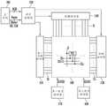
图1图示了有机发光显示设备的实施例,该有机发光显示设备包括像素单元100、第一扫描驱动器110、第二扫描驱动器120、控制驱动器130、数据驱动器140、时序控制器150、主系统160、第一电力驱动器170和第二电力驱动器180。在实施例中,用于驱动有机发光显示设备的一个帧周期1F被划分为第一时段T1、第二时段T2、第三时段T3和第四时段T4,例如,如图4所示。1 illustrates an embodiment of an organic light emitting display device, which includes a
第一时段T1至第三时段T3用于初始化像素PXL,并且像素PXL中的全部在第一时段T1至第三时段T3中同时被驱动。第四时段T4为像素PXL发光的时段。像素PXL可以在第四时段T4中以水平行为单位依次被驱动。The first to third periods T1 to T3 are used to initialize the pixels PXL, and all of the pixels PXL are simultaneously driven in the first to third periods T1 to T3. The fourth period T4 is a period in which the pixel PXL emits light. The pixels PXL may be sequentially driven in units of horizontal rows in the fourth period T4.
数据驱动器140基于来自时序控制器150的图像数据生成数据信号。在第四时段T4期间,由数据驱动器140生成的数据信号被供给到数据线D,并且与依次供给到第一扫描线S1的第一扫描信号同步。数据驱动器140可以在数据信号之间供给恒定电压。恒定电压可以是例如用于初始化数据线D的预设的预定电压。The
第一扫描驱动器110将第一扫描信号供给到第一扫描线S1。例如,第一扫描驱动器110可以在第二时段T2和第三时段T3期间将第一扫描信号同时供给到第一扫描线S1,并且可以在第四时段T4期间将第一扫描信号依次供给到第一扫描线S1。当第一扫描信号被供给到第一扫描线S1时,像素PXL中的每一个中的晶体管被导通。第一扫描信号可以被设置为栅极导通电压(例如,高电压),以使像素PXL中的每一个中的晶体管导通。The
第二扫描驱动器120将第二扫描信号供给到第二扫描线S2。例如,第二扫描驱动器120可以在第二时段T2和第三时段T3期间将第二扫描信号同时供给到第二扫描线S2。当第二扫描信号被供给到第二扫描线S2时,像素PXL中的每一个中的晶体管被导通。第二扫描信号被设置为栅极导通电压(例如,高电压),以使像素PXL中的每一个中的晶体管导通。The
控制驱动器130将控制信号(例如,高电压)供给到控制线CL。例如,控制驱动器130可以在第一时段T1和第二时段T2期间将控制信号同时供给到控制线CL,并且可以在第四时段T4期间将控制信号依次供给到控制线CL。在第四时段T4期间,对应于供给到控制线CL的控制信号来控制像素PXL的发射时间。The
另外,控制驱动器130在第一时段T1和第二时段T2期间将具有第一宽度W1的控制信号同时供给到控制线CL。控制驱动器130还在第四时段T4期间将具有第二宽度W2的控制信号依次供给到控制线CL。第二宽度W2可以大于第一宽度W1。In addition, the
时序控制器150基于来自主系统160的时序信号,控制驱动器110、120、130、140、170和180。从主系统160输出的时序信号和其他信号的示例包括图像数据RGB、垂直同步信号Vsync、水平同步信号Hsync、数据使能信号DE和时钟信号CLK。The
主系统160通过预定接口将图像数据RGB供给到时序控制器150。主系统160将时序信号Vsync、Hsync、DE和CLK供给到时序控制器150。The
第一电力驱动器170将第一电源ELVDD供给到像素PXL。第一电力驱动器170在第一时段T1和第二时段T2期间供给具有第一电压V1的第一电源ELVDD,并且在第三时段T3期间供给具有第二电压V2的第一电源ELVDD。第一电力驱动器170在第四时段T4期间供给具有第三电压V3的第一电源ELVDD。第一电压V1可以等于或小于第二电源ELVSS的电压。第二电压V2可以小于第一电压V1。第三电压V3可以大于第一电压V1,例如,像素PXL发光的电压。The
第二电力驱动器180将第二电源ELVSS供给到像素PXL。第二电源ELVSS可以在一个帧周期1F期间保持恒定电压。The
像素单元100包括耦接到数据线D、第一扫描线S1、第二扫描线S2和控制线CL的多个像素PXL。每个像素PXL发射具有与数据信号中的相应一个数据信号相对应的预定亮度的光。The
耦接到第i(i为自然数)水平行上的像素PXL的第二扫描线S2i可以被设置为第(i+1)条第一扫描线S1i+1。在一个实施例中,第二扫描驱动器120和第二扫描线S2可以被移除,如图2所示。The second scan line S2i coupled to the pixel PXL on the i-th (i is a natural number) horizontal row may be set as the (i+1)th first scan
图3图示了像素的实施例,该像素例如可以代表图2所示的像素PXL。在图3中,为了便于描述,图示了第i水平行上的像素PXL。另外,假定耦接到第i水平行上的像素PXL的第二扫描线S2i被设置为第(i+1)条第一扫描线S1i+1。FIG. 3 illustrates an embodiment of a pixel, which may represent, for example, the pixel PXL shown in FIG. 2 . In FIG. 3 , for convenience of description, the pixel PXL on the i-th horizontal row is illustrated. Also, assume that the second scan line S2i coupled to the pixel PXL on the i-th horizontal row is set as the (i+1)th first scan
参考图3,像素PXL包括有机发光二极管OLED和像素电路210,像素电路210用于控制供给到有机发光二极管OLED的电流的量。有机发光二极管OLED具有耦接到像素电路210的阳极和耦接到第二电源ELVSS的阴极。有机发光二极管OLED产生具有与从像素电路210供给的电流的量相对应的预定亮度的光。像素电路210基于数据信号控制供给到有机发光二极管OLED的电流的量。Referring to FIG. 3 , the pixel PXL includes an organic light emitting diode OLED and a
像素电路210包括第一晶体管M1、第二晶体管M2、第三晶体管M3、第一电容器C1和第二电容器C2。第一晶体管(或驱动晶体管)M1耦接在第一电源ELVDD与第一节点N1之间。第一节点N1电耦接到有机发光二极管OLED的阳极。第一晶体管M1的栅电极耦接到第二节点N2。第一晶体管M1基于第二节点N2的电压,控制经由有机发光二极管OLED从第一电源ELVDD流到第二电源ELVSS的电流的量。The
第二晶体管M2耦接在第二节点N2与第三节点N3之间。第二晶体管M2的栅电极耦接到第i条第一扫描线S1i。当第一扫描信号被供给到第i条第一扫描线S1i时,第二晶体管M2被导通,以便允许第二节点N2和第三节点N3彼此电耦接。The second transistor M2 is coupled between the second node N2 and the third node N3. The gate electrode of the second transistor M2 is coupled to the i-th first scan line S1i. When the first scan signal is supplied to the i-th first scan line S1i, the second transistor M2 is turned on so as to allow the second node N2 and the third node N3 to be electrically coupled to each other.
第三晶体管M3耦接在第三节点N3与第一节点N1之间。第三晶体管M3的栅电极耦接到第(i+1)条第一扫描线S1i+1(或第i条第二扫描线S2i)。当第一扫描信号被供给到第(i+1)条第一扫描线S1i+1时,第三晶体管M3被导通,以便允许第三节点N3和第一节点N1彼此电耦接。在一个实施例中,第一晶体管M1至第三晶体管M3可以是N型晶体管(例如,NMOS晶体管)。The third transistor M3 is coupled between the third node N3 and the first node N1. The gate electrode of the third transistor M3 is coupled to the (i+1)th first scan line S1i+1 (or the i-th second scan line S2i). When the first scan signal is supplied to the (i+1)th first scan line S1i+1, the third transistor M3 is turned on so as to allow the third node N3 and the first node N1 to be electrically coupled to each other. In one embodiment, the first transistor M1 to the third transistor M3 may be N-type transistors (eg, NMOS transistors).
第一电容器C1耦接在第i控制线CLi与第二节点N2之间。第一电容器C1基于供给到第i控制线CLi的控制信号,控制第二节点N2的电压。当晶体管M1至M3为N型晶体管时,控制信号被设置成增大第二节点N2的电压。The first capacitor C1 is coupled between the i-th control line CLi and the second node N2. The first capacitor C1 controls the voltage of the second node N2 based on the control signal supplied to the i-th control line CLi. When the transistors M1 to M3 are N-type transistors, the control signal is set to increase the voltage of the second node N2.
第二电容器C2耦接在数据线Dm与第三节点N3之间。第二电容器C2对应于供给到数据线Dm的数据信号的电压,控制第三节点N3的电压。The second capacitor C2 is coupled between the data line Dm and the third node N3. The second capacitor C2 controls the voltage of the third node N3 corresponding to the voltage of the data signal supplied to the data line Dm.
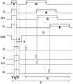
图4图示了用于驱动图3所示的像素的方法的实施例的波形图。参考图4,首先,控制信号在一个帧周期1F中的第一时段T1和第二时段T2期间被供给到控制线CL1至CLn。此外,第一电源ELVDD的电压在第一时段T1和第二时段T2期间下降到第一电压V1。FIG. 4 illustrates a waveform diagram of an embodiment of a method for driving the pixel shown in FIG. 3 . Referring to FIG. 4 , first, a control signal is supplied to the control lines CL1 to CLn during a first period T1 and a second period T2 in one
当控制信号被供给到第i控制线CLi时,第i控制线CLi的电压增大。因此,第二节点N2的电压增大。当第二节点N2的电压增大时,第一晶体管M1被导通。控制信号的电压可以被设置成使第一晶体管M1导通,而不管在前一帧周期中施加的第二节点N2的电压。When the control signal is supplied to the i-th control line CLi, the voltage of the i-th control line CLi increases. Accordingly, the voltage of the second node N2 increases. When the voltage of the second node N2 increases, the first transistor M1 is turned on. The voltage of the control signal may be set to turn on the first transistor M1 regardless of the voltage of the second node N2 applied in the previous frame period.
当第一晶体管M1被导通时,第一电源ELVDD电耦接到有机发光二极管OLED的阳极。此时,第一电源ELVDD被设置成等于或小于第二电源ELVSS的电压的电压。因此,在有机发光二极管OLED中等效形成的有机电容器Coled放电。结果是,有机发光二极管OLED的阳极在第一时段T1期间被初始化成近似第一电压V1。When the first transistor M1 is turned on, the first power source ELVDD is electrically coupled to the anode of the organic light emitting diode OLED. At this time, the first power source ELVDD is set to a voltage equal to or lower than the voltage of the second power source ELVSS. Accordingly, the organic capacitor Coled, which is equivalently formed in the organic light emitting diode OLED, is discharged. As a result, the anode of the organic light emitting diode OLED is initialized to approximately the first voltage V1 during the first period T1.
第一扫描信号在第二时段T2和第三时段T3期间同时被供给到第一扫描线S11至S1n。当第一扫描信号被供给到第i条第一扫描线S1i和第(i+1)条第一扫描线S1i+1时,第二晶体管M2和第三晶体管M3被导通。The first scan signal is simultaneously supplied to the first scan lines S11 to S1n during the second period T2 and the third period T3. When the first scan signal is supplied to the i-th first scan line S1i and the (i+1)-th first scan line S1i+1, the second transistor M2 and the third transistor M3 are turned on.
当第二晶体管M2和第三晶体管M3被导通时,第二节点N2和第一节点N1彼此电耦接。于是,第二节点N2通过有机电容器Coled的电压被初始化成近似第一电压V1。When the second transistor M2 and the third transistor M3 are turned on, the second node N2 and the first node N1 are electrically coupled to each other. Then, the voltage of the second node N2 is initialized to approximately the first voltage V1 through the organic capacitor Coled.
在第三时段T3中停止控制信号到控制线CL1至CLn的供给。另外,第一电源ELVDD的电压下降到小于第一电压V1的第二电压V2。第二电压V2被设置,使得第一晶体管M1能够保持导通状态,而不管控制信号的供给是否停止。The supply of the control signal to the control lines CL1 to CLn is stopped in the third period T3. In addition, the voltage of the first power source ELVDD drops to a second voltage V2 that is lower than the first voltage V1. The second voltage V2 is set such that the first transistor M1 can maintain a turn-on state regardless of whether the supply of the control signal is stopped.
当第一晶体管M1被设置成导通状态时,预定电流经由二极管耦接的第一晶体管M1从第二节点N2被供给到第一电源ELVDD。在此情形下,与第一晶体管M1的阈值电压相对应的电压被施加到第二节点N2。When the first transistor M1 is set to a turn-on state, a predetermined current is supplied from the second node N2 to the first power source ELVDD via the diode-coupled first transistor M1. In this case, a voltage corresponding to the threshold voltage of the first transistor M1 is applied to the second node N2.
第一电容器C1在第三时段T3期间存储第i控制线CLi与第二节点N2之间的电压。也就是说,与第一晶体管M1的阈值电压相对应的电压在第三时段T3期间被存储在第一电容器C1中。The first capacitor C1 stores a voltage between the i-th control line CLi and the second node N2 during the third period T3. That is, a voltage corresponding to the threshold voltage of the first transistor M1 is stored in the first capacitor C1 during the third period T3.
像素PXL中的全部在第一时段T1至第三时段T3期间同时被驱动。因此,与第一晶体管M1的阈值电压相对应的电压在第一时段T1至第三时段T3期间被存储在像素PXL中的每一个中的第一电容器C1中。All of the pixels PXL are simultaneously driven during the first to third periods T1 to T3. Accordingly, a voltage corresponding to the threshold voltage of the first transistor M1 is stored in the first capacitor C1 in each of the pixels PXL during the first to third periods T1 to T3.
此外,像素PXL在第一时段T1至第三时段T3期间同时被驱动。因此,可以将足够的时间分配给第一时段T1至第三时段T3,以允许稳定地补偿像素PXL的阈值电压。这可以允许形成具有高分辨率面板的显示设备。In addition, the pixels PXL are simultaneously driven during the first period T1 to the third period T3. Therefore, sufficient time may be allocated to the first period T1 to the third period T3 to allow the threshold voltage of the pixel PXL to be stably compensated. This may allow the formation of display devices with high resolution panels.
第一电源ELVDD在第四时段T4期间被设置成大于第一电压V1的第三电压V3。第三电压V3被设置使得像素PXL基于对应的数据信号发光。The first power supply ELVDD is set to a third voltage V3 greater than the first voltage V1 during the fourth period T4. The third voltage V3 is set such that the pixel PXL emits light based on the corresponding data signal.
第一扫描信号在第四时段T4期间依次被供给到第一扫描线S11至S1n。当第一扫描信号被供给到第i条第一扫描线S1i时,第二晶体管M2被导通。当第二晶体管M2被导通时,第二节点N2和第三节点N3彼此电耦接。The first scan signal is sequentially supplied to the first scan lines S11 to S1n during the fourth period T4. When the first scan signal is supplied to the i-th first scan line S1i, the second transistor M2 is turned on. When the second transistor M2 is turned on, the second node N2 and the third node N3 are electrically coupled to each other.
同时,数据信号被供给到数据线Dm,以同步于被供给到第i条第一扫描线S1i的第一扫描信号。当数据信号被供给到数据线Dm时,第三节点N3的电压和第二节点N2的电压由于第二电容器C2的耦合而改变。在此情形下,对应于供给到数据线Dm的数据信号的电压,而确定第二节点N2的电压变化。因此,与数据信号相对应的电压被附加地存储在第一电容器C1中。Meanwhile, the data signal is supplied to the data line Dm in synchronization with the first scan signal supplied to the i-th first scan line S1i. When the data signal is supplied to the data line Dm, the voltage of the third node N3 and the voltage of the second node N2 are changed due to the coupling of the second capacitor C2. In this case, the voltage variation of the second node N2 is determined corresponding to the voltage of the data signal supplied to the data line Dm. Accordingly, a voltage corresponding to the data signal is additionally stored in the first capacitor C1.
在与数据信号相对应的电压被存储在第一电容器C1中之后,第三晶体管M3基于供给到第(i+1)条第一扫描线S1i+1的第一扫描信号被导通。此时,由于第二晶体管M2保持截止状态,因此第二节点N2的电压不会对应于供给到数据线Dm的数据信号而改变。因此,第一电容器C1可以稳定地保持在前一个时段中存储的数据信号的电压。After the voltage corresponding to the data signal is stored in the first capacitor C1, the third transistor M3 is turned on based on the first scan signal supplied to the (i+1)th first scan
在与数据信号相对应的电压被存储在第一电容器C1中之后,控制信号被供给到第i控制线CLi。当控制信号被供给到第i控制线CLi时,第二节点N2的电压增大。此时,第一晶体管M1将与第二节点N2的电压相对应的电流供给到有机发光二极管OLED。因此,有机发光二极管OLED产生具有预定亮度的光。当与黑色数据信号相对应的电压被存储在第一电容器C1中时,第一晶体管M1保持截止状态,而不管控制信号是否被供给。After the voltage corresponding to the data signal is stored in the first capacitor C1, the control signal is supplied to the i-th control line CLi. When the control signal is supplied to the i-th control line CLi, the voltage of the second node N2 increases. At this time, the first transistor M1 supplies a current corresponding to the voltage of the second node N2 to the organic light emitting diode OLED. Accordingly, the organic light emitting diode OLED generates light with a predetermined brightness. When the voltage corresponding to the black data signal is stored in the first capacitor C1, the first transistor M1 maintains an off state regardless of whether the control signal is supplied.
同时,供给到第i控制线CLi的控制信号被设置成第二宽度W2。因此,在第i水平行上的像素PXL在第四时段T4期间被设置成发射状态。更具体地,像素PXL以水平行为单位存储与数据信号相对应的电压,并且对应于控制信号而依次发光。Meanwhile, the control signal supplied to the i-th control line CLi is set to the second width W2. Accordingly, the pixels PXL on the i-th horizontal row are set to an emission state during the fourth period T4. More specifically, the pixels PXL store voltages corresponding to data signals in units of horizontal rows, and sequentially emit light corresponding to control signals.
图5图示了一个帧周期的实施例,帧周期例如可以与图4的驱动方法相对应。在图5中,图示了像素PXL中的全部发射与数据信号相对应的光的情形。FIG. 5 illustrates an embodiment of a frame period, which may correspond to, for example, the driving method of FIG. 4 . In FIG. 5 , a case where all of the pixels PXL emit light corresponding to a data signal is illustrated.
参考图5,像素PXL在第一时段T1至第三时段T3期间同时被驱动。此时,与像素PXL中的每一个中的第一晶体管M1的阈值电压相对应的电压在整个第一时段T1至第三时段T3期间被存储在相关联的第一电容器C1中。Referring to FIG. 5 , the pixels PXL are simultaneously driven during the first period T1 to the third period T3 . At this time, a voltage corresponding to the threshold voltage of the first transistor M1 in each of the pixels PXL is stored in the associated first capacitor C1 throughout the first to third periods T1 to T3.
另外,像素PXL在第四时段T4期间依次被驱动。此时,对应数据信号的电压在第四时段T4期间以水平行为单位被存储在像素PXL中。在数据信号的电压被存储在像素PXL中之后,像素PXL以水平行为单位依次发光。此时,像素PXL的发射时间被设置成彼此相等,而不管水平行的位置。In addition, the pixels PXL are sequentially driven during the fourth period T4. At this time, the voltage corresponding to the data signal is stored in the pixel PXL in units of horizontal rows during the fourth period T4. After the voltage of the data signal is stored in the pixel PXL, the pixel PXL sequentially emits light in units of horizontal rows. At this time, the emission times of the pixels PXL are set to be equal to each other regardless of the position of the horizontal line.
图6图示了图2所示的像素的另一实施例。在图6中,与图3的组件相同的组件由相同的附图标记指定。FIG. 6 illustrates another embodiment of the pixel shown in FIG. 2 . In FIG. 6, the same components as those of FIG. 3 are designated by the same reference numerals.
参考图6,像素PXL包括有机发光二极管OLED和像素电路212,像素电路212用于控制供给到有机发光二极管OLED的电流的量。Referring to FIG. 6, the pixel PXL includes an organic light emitting diode OLED and a
有机发光二极管OLED具有耦接到像素电路212的阳极和耦接到第二电源ELVSS的阴极。有机发光二极管OLED产生具有与从像素电路212供给的电流的量相对应的预定亮度的光。像素电路212基于数据信号,控制供给到有机发光二极管OLED的电流的量。The organic light emitting diode OLED has an anode coupled to the
像素电路212包括第一晶体管M1、第二晶体管M2_1和M2_2、第三晶体管M3_1和M3_2、第一电容器C1和第二电容器C2。第二晶体管M2_1和M2_2串联耦接在第二节点N2与第三节点N3之间。第二晶体管M2_1和M2_2的栅电极耦接到第i条第一扫描线S1i。当第一扫描信号被供给到第i条第一扫描线S1i时,第二晶体管M2_1和M2_2被导通,以允许第二节点N2和第三节点N3彼此电耦接。The
另外,将第二晶体管M2_1和M2_2串联耦接在第二节点N2与第三节点N3之间可以允许第二节点N2与第三节点N3之间的漏电流降低或最小化。这可以改善驱动稳定性。In addition, coupling the second transistors M2_1 and M2_2 in series between the second node N2 and the third node N3 may allow the leakage current between the second node N2 and the third node N3 to be reduced or minimized. This can improve drive stability.
第三晶体管M3_1和M3_2串联耦接在第三节点N3与第一节点N1之间。第三晶体管M3_1和M3_2的栅电极耦接到第(i+1)条第一扫描线S1i+1。当第一扫描信号被供给到第(i+1)条第一扫描线S1i+1时,第三晶体管M3_1和M3_2被导通,以允许第三节点N3和第一节点N1彼此电耦接。The third transistors M3_1 and M3_2 are coupled in series between the third node N3 and the first node N1. Gate electrodes of the third transistors M3_1 and M3_2 are coupled to the (i+1)th first scan
另外,将第三晶体管M3_1和M3_2串联耦接在第三节点N3与第一节点N1之间可以允许第三节点N3与第一节点N1之间的漏电流降低或最小化。这可以改善驱动稳定性。In addition, coupling the third transistors M3_1 and M3_2 in series between the third node N3 and the first node N1 may allow a leakage current between the third node N3 and the first node N1 to be reduced or minimized. This can improve drive stability.
除了像素电路212具有多个第二晶体管M2_1和M2_2以及多个第三晶体管M3_1和M3_2之外,用于操作本实施例中的像素PXL的过程可以与用于操作图3的像素PXL的过程基本相同。The process for operating the pixel PXL in this embodiment can be basically the same as the process for operating the pixel PXL in FIG. same.
此外,在图6中,提供了两个第二晶体管M2_1和M2_2以及两个第三晶体管M3_1和M3_2。在另一实施例中,可以串联耦接多于两个第二晶体管M2_1和M2_2和/或多于两个第三晶体管M3_1和M3_2。Furthermore, in FIG. 6 , two second transistors M2_1 and M2_2 and two third transistors M3_1 and M3_2 are provided. In another embodiment, more than two second transistors M2_1 and M2_2 and/or more than two third transistors M3_1 and M3_2 may be coupled in series.
图7图示了有机发光显示设备的另一实施例。在图7中,与图1的组件相同的组件由相同的附图标记指定。FIG. 7 illustrates another embodiment of an organic light emitting display device. In FIG. 7, the same components as those of FIG. 1 are designated by the same reference numerals.
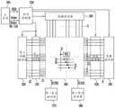
参考图7,有机发光显示设备包括像素单元100'、第一扫描驱动器110、第二扫描驱动器120、控制驱动器130'、数据驱动器140、时序控制器150、主系统160、第一电力驱动器170和第二电力驱动器180。Referring to FIG. 7, an organic light emitting display device includes a pixel unit 100', a
像素单元100'被划分为多个块BL1至BLj。每个块BL包括设置在至少两个水平行上的像素PXL。在同一个块BL中的像素PXL耦接到同一条控制线CL。在其他块BL中的像素PXL耦接到其他控制线CL。例如,在第一个块BL1中的像素PXL可以共同地耦接到第一控制线CL1,并且第k(k为自然数)个块BLk中的像素PXL可以共同地耦接到第k控制线CLk。在此情形下,像素PXL的发射时间以块BL为单位被控制。例如,像素PXL可以以块BL为单位依次发光。The pixel unit 100' is divided into a plurality of blocks BL1 to BLj. Each block BL includes pixels PXL arranged on at least two horizontal lines. Pixels PXL in the same block BL are coupled to the same control line CL. Pixels PXL in other blocks BL are coupled to other control lines CL. For example, the pixels PXL in the first block BL1 may be commonly coupled to the first control line CL1, and the pixels PXL in the kth (k is a natural number) block BLk may be commonly coupled to the kth control line CLk. . In this case, the emission time of the pixel PXL is controlled in units of blocks BL. For example, the pixels PXL may sequentially emit light in units of blocks BL.
图8的像素PXL中的每个包括可以与图3的像素电路210基本相同的像素电路210'。耦接到第i条第一扫描线S1i的像素PXL可以耦接到第k控制线CLk。Each of the pixels PXL of FIG. 8 includes a
图9图示了用于驱动图8的像素的方法的另一实施例的波形图。在图8中,假定第i条第一扫描线S1i、第(i+1)条第一扫描线S1i+1和第(i+2)条第一扫描线S1i+2在同一个块中。FIG. 9 illustrates a waveform diagram of another embodiment of a method for driving the pixel of FIG. 8 . In FIG. 8 , it is assumed that the i-th first scan line S1i, the (i+1)-th first scan line S1i+1, and the (i+2)-th first scan line S1i+2 are in the same block.
参考图9,首先,控制信号在一个帧周期1F中的第十一时段T11和第十二时段T12期间被供给到控制线CL1至CLj。另外,第一电源ELVDD的电压在第十一时段T11和第十二时段T12期间下降到第一电压V1。Referring to FIG. 9 , first, control signals are supplied to the control lines CL1 to CLj during the eleventh period T11 and the twelfth period T12 in one
当控制信号被供给到第k控制线CLk时,第k控制线CLk的电压增大。因此,第二节点N2的电压增大。当第二节点N2的电压增大时,第一晶体管M1被导通。When the control signal is supplied to the kth control line CLk, the voltage of the kth control line CLk increases. Accordingly, the voltage of the second node N2 increases. When the voltage of the second node N2 increases, the first transistor M1 is turned on.
当第一晶体管M1被导通时,第一电源ELVDD和有机发光二极管OLED的阳极彼此电耦接。此时,第一电源ELVDD被设置成等于或小于第二电源ELVSS的电压的第一电压V1。因此,有机电容器Coled放电。When the first transistor M1 is turned on, the first power source ELVDD and the anode of the organic light emitting diode OLED are electrically coupled to each other. At this time, the first power source ELVDD is set to a first voltage V1 equal to or lower than the voltage of the second power source ELVSS. Therefore, the organic capacitor Coled is discharged.
第一扫描信号在第十二时段T12和第十三时段T13期间同时被供给到第一扫描线S11至S1n。当第一扫描信号被供给到第i条第一扫描线S1i和第(i+1)条第一扫描线S1i+1时,第二晶体管M2和第三晶体管M3被导通。The first scan signal is simultaneously supplied to the first scan lines S11 to S1n during the twelfth period T12 and the thirteenth period T13. When the first scan signal is supplied to the i-th first scan line S1i and the (i+1)-th first scan line S1i+1, the second transistor M2 and the third transistor M3 are turned on.
当第二晶体管M2和第三晶体管M3被导通时,第二节点N2和第一节点N1彼此电耦接。于是,第二节点N2通过有机电容器Coled的电压而被初始化成近似第一电压V1。When the second transistor M2 and the third transistor M3 are turned on, the second node N2 and the first node N1 are electrically coupled to each other. Then, the second node N2 is initialized to approximately the first voltage V1 by the voltage of the organic capacitor Coled.
在第十三时段T13中停止控制信号到控制线CL1至CLj的供给。另外,第一电源ELVDD的电压在第十三时段T13中下降到小于第一电压V1的第二电压V2。于是,预定电流经由二极管耦接的第一晶体管M1从第二节点N2被供给到第一电源ELVDD。在此情形下,与第一晶体管M1的阈值电压相对应的电压被施加到第二节点N2。The supply of the control signal to the control lines CL1 to CLj is stopped in the thirteenth period T13. In addition, the voltage of the first power source ELVDD drops to the second voltage V2 which is lower than the first voltage V1 in the thirteenth period T13. Accordingly, a predetermined current is supplied from the second node N2 to the first power source ELVDD via the diode-coupled first transistor M1. In this case, a voltage corresponding to the threshold voltage of the first transistor M1 is applied to the second node N2.
第一电容器C1在第十三时段T13期间存储第k控制线CLk与第二节点N2之间的电压,例如,与第一晶体管M1的阈值电压相对应的电压在第十三时段T13期间被存储在第一电容器C1中。The first capacitor C1 stores a voltage between the kth control line CLk and the second node N2 during the thirteenth period T13, for example, a voltage corresponding to the threshold voltage of the first transistor M1 is stored during the thirteenth period T13. in the first capacitor C1.
像素PXL中的全部在第十一时段T11至第十三时段T13期间同时被驱动。因此,与第一晶体管M1的阈值电压相对应的电压在第十一时段T11至第十三时段T13期间被存储在像素PXL中的每一个中的第一电容器C1中。All of the pixels PXL are simultaneously driven during the eleventh period T11 to the thirteenth period T13. Accordingly, a voltage corresponding to the threshold voltage of the first transistor M1 is stored in the first capacitor C1 in each of the pixels PXL during the eleventh period T11 to the thirteenth period T13 .
第一电源ELVDD在第十四时段T14期间被设置成大于第一电压V1的第三电压V3。第三电压V3可以被设置使得像素PXL对应于数据信号而发光。The first power supply ELVDD is set to a third voltage V3 greater than the first voltage V1 during the fourteenth period T14. The third voltage V3 may be set such that the pixel PXL emits light corresponding to the data signal.
第一扫描信号在第十四时段T14期间依次被供给到第一扫描线S11至S1n。当第一扫描信号被供给到第i条第一扫描线S1i时,第二晶体管M2被导通。当第二晶体管M2被导通时,第二节点N2电耦接到第三节点N3。The first scan signal is sequentially supplied to the first scan lines S11 to S1n during the fourteenth period T14. When the first scan signal is supplied to the i-th first scan line S1i, the second transistor M2 is turned on. When the second transistor M2 is turned on, the second node N2 is electrically coupled to the third node N3.
数据信号被供给到数据线Dm,以同步于被供给到第i条第一扫描线S1i的第一扫描信号。当数据信号被供给到数据线Dm时,第三节点N3的电压和第二节点N2的电压由于第二电容器C2的耦合而改变。在此情形下,对应于供给到数据线Dm的数据信号的电压,来确定第二节点N2的电压变化。因此,与数据信号相对应的电压被附加地存储在第一电容器C1中。The data signal is supplied to the data line Dm in synchronization with the first scan signal supplied to the i-th first scan line S1i. When the data signal is supplied to the data line Dm, the voltage of the third node N3 and the voltage of the second node N2 are changed due to the coupling of the second capacitor C2. In this case, the voltage variation of the second node N2 is determined corresponding to the voltage of the data signal supplied to the data line Dm. Accordingly, a voltage corresponding to the data signal is additionally stored in the first capacitor C1.
在第一扫描信号被供给到第i条第一扫描线S1i之后,第一扫描信号被供给到第(i+1)条第一扫描线S1i+1。当第一扫描信号被供给到第(i+1)条第一扫描线S1i+1时,第(i+1)条水平行上的像素PXL存储与数据信号相对应的电压。After the first scan signal is supplied to the i-th first scan line S1i, the first scan signal is supplied to the (i+1)-th first scan
在第一扫描信号被供给到第(i+1)条第一扫描线S1i+1之后,第一扫描信号被供给到第(i+2)条第一扫描线S1i+2。当第一扫描信号被供给到第(i+2)条第一扫描线S1i+2时,第(i+2)水平行上的像素PXL存储与数据信号相对应的电压。After the first scan signal is supplied to the (i+1)th first scan line S1i+1, the first scan signal is supplied to the (i+2)th first scan
在第一扫描信号被供给到同一个块BL中的第i条第一扫描线S1i、第(i+1)条第一扫描线S1i+1和第(i+2)条第一扫描线S1i+2之后,控制信号被供给到电耦接到同一个块BL中的像素PXL的第k控制线CLk。When the first scan signal is supplied to the i-th first scan line S1i, the (i+1)-th first scan line S1i+1, and the (i+2)-th first scan line S1i in the same block BL After +2, the control signal is supplied to the kth control line CLk electrically coupled to the pixel PXL in the same block BL.
当控制信号被供给到第k控制线CLk时,耦接到第i条第一扫描线S1i、第(i+1)条第一扫描线S1i+1和第(i+2)条第一扫描线S1i+2的像素PXL中的每一个中的第二节点N2的电压增大。此时,第一晶体管M1将与第二节点N2的电压相对应的电流供给到有机发光二极管OLED。因此,有机发光二极管OLED产生具有预定亮度的光。When the control signal is supplied to the k-th control line CLk, it is coupled to the i-th first scan line S1i, the (i+1)-th first scan line S1i+1, and the (i+2)-th first scan line The voltage of the second node N2 in each of the pixels PXL of the line S1i+2 increases. At this time, the first transistor M1 supplies a current corresponding to the voltage of the second node N2 to the organic light emitting diode OLED. Accordingly, the organic light emitting diode OLED generates light with a predetermined brightness.
因此,在本实施例中,同一个块BL中的像素PXL同时发光或同时不发光。另外,像素PXL以块BL为单位依次发光。另外,在第十四时段T14期间供给到控制线CL1至CLj的控制信号的宽度彼此相等。因此,像素PXL的发射时间彼此相等,而不管块BL的位置。Therefore, in this embodiment, the pixels PXL in the same block BL emit light at the same time or do not emit light at the same time. In addition, the pixels PXL sequentially emit light in units of blocks BL. In addition, the widths of the control signals supplied to the control lines CL1 to CLj during the fourteenth period T14 are equal to each other. Therefore, the emission times of the pixels PXL are equal to each other regardless of the position of the block BL.
图10图示了有机发光显示设备的另一实施例。在图10中,与图1的组件相同的组件由相同的附图标记指定。FIG. 10 illustrates another embodiment of an organic light emitting display device. In FIG. 10 , the same components as those of FIG. 1 are designated by the same reference numerals.
参考图10,有机发光显示设备包括像素单元100、第一扫描驱动器110、第二扫描驱动器120'、控制驱动器130、数据驱动器140、时序控制器150、主系统160、第一电力驱动器170和第二电力驱动器180。Referring to FIG. 10 , an organic light emitting display device includes a
第二扫描线S2共同耦接到像素PXL,并且供给来自第二扫描驱动器120'的第二扫描信号。第二扫描驱动器120'将第二扫描信号供给到第二扫描线S2。例如,第二扫描驱动器120'可以在一个帧周期1F中的第二十二时段T22和第二十三时段T23期间将第二扫描信号供给到第二扫描线S2,例如如图12所示。第二扫描信号被设置为栅极导通电压,以使像素PXL中的每一个中的晶体管导通。The second scan line S2 is commonly coupled to the pixels PXL, and supplies the second scan signal from the second scan driver 120'. The second scan driver 120' supplies the second scan signal to the second scan line S2. For example, the second scan driver 120' may supply the second scan signal to the second scan line S2 during the twenty-second period T22 and the twenty-third period T23 in one
图11图示了像素的另一实施例,该像素例如可以是图10的像素PXL的例示。在图11中,与图3的组件相同的组件由相同的附图标记指定。FIG. 11 illustrates another embodiment of a pixel, which may be, for example, an instance of pixel PXL of FIG. 10 . In FIG. 11 , the same components as those of FIG. 3 are designated by the same reference numerals.
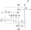
参考图11,像素PXL包括有机发光二极管OLED和像素电路214,像素电路214用于控制供给到有机发光二极管OLED的电流的量。有机发光二极管OLED具有耦接到像素电路214的阳极和耦接到第二电源ELVSS的阴极。有机发光二极管OLED产生具有与从像素电路214供给的电流的量相对应的预定亮度的光。像素电路214根据数据信号,控制供给到有机发光二极管OLED的电流的量。Referring to FIG. 11 , the pixel PXL includes an organic light emitting diode OLED and a
像素电路214包括第一晶体管M1、第二晶体管M2、第三晶体管M3'、第一电容器C1和第二电容器C2。第三晶体管M3'耦接在第三节点N3与第一节点N1之间。第三晶体管M3'的栅电极耦接到第二扫描线S2。当第二扫描信号被供给到第二扫描线S2时,第三晶体管M3'被导通,以允许第三节点N3和第一节点N1彼此电耦接。The
图12图示了用于驱动像素(其例如可以是图11的像素)的方法的另一实施例的波形图。FIG. 12 illustrates a waveform diagram of another embodiment of a method for driving a pixel (which may be, for example, the pixel of FIG. 11 ).
参考图12,首先,控制信号在一个帧周期1F中的第二十一时段T21和第二十二时段T22期间被供给到控制线CL1至CLn。第一电源ELVDD的电压在第二十一时段T21和第二十二时段T22期间下降到第一电压V1。Referring to FIG. 12 , first, control signals are supplied to the control lines CL1 to CLn during the twenty-first period T21 and the twenty-second period T22 in one
当控制信号被供给到第i控制线CLi时,第i控制线CLi的电压增大。因此,第二节点N2的电压增大。当第二节点N2的电压增大时,第一晶体管M1被导通。When the control signal is supplied to the i-th control line CLi, the voltage of the i-th control line CLi increases. Accordingly, the voltage of the second node N2 increases. When the voltage of the second node N2 increases, the first transistor M1 is turned on.
当第一晶体管M1被导通时,第一电源ELVDD和有机发光二极管OLED的阳极彼此电耦接。因此,有机电容器Coled放电。When the first transistor M1 is turned on, the first power source ELVDD and the anode of the organic light emitting diode OLED are electrically coupled to each other. Therefore, the organic capacitor Coled is discharged.
第一扫描信号在第二十二时段T22和第二十三时段T23期间同时被供给到第一扫描线S11至S1n。第二扫描信号在第二十二时段T22和第二十三时段T23期间被供给到第二扫描线S2。当第一扫描信号被供给到第一扫描线S11至S1n时,像素PXL中的每一个中的第二晶体管M2被导通。当第二扫描信号被供给到第二扫描线S2时,像素PXL中的每一个中的第三晶体管M3'被导通。The first scan signal is simultaneously supplied to the first scan lines S11 to S1n during the twenty-second period T22 and the twenty-third period T23. The second scan signal is supplied to the second scan line S2 during the twenty-second period T22 and the twenty-third period T23. When the first scan signal is supplied to the first scan lines S11 to S1n, the second transistor M2 in each of the pixels PXL is turned on. When the second scan signal is supplied to the second scan line S2, the third transistor M3' in each of the pixels PXL is turned on.
当第二晶体管M2和第三晶体管M3'被导通时,第二节点N2和第一节点N1彼此电耦接。于是,第二节点N2通过有机电容器Coled的电压被初始化成近似第一电压V1。When the second transistor M2 and the third transistor M3' are turned on, the second node N2 and the first node N1 are electrically coupled to each other. Then, the voltage of the second node N2 is initialized to approximately the first voltage V1 through the organic capacitor Coled.
在第二十三时段T23中停止控制信号到控制线CL1至CLn的供给。另外,第一电源ELVDD的电压在第二十三时段T23中下降到小于第一电压V1的第二电压V2。于是,预定电流经由二极管耦接的第一晶体管M1从第二节点N2被供给到第一电源ELVDD。在此情形下,与第一晶体管M1的阈值电压相对应的电压被施加到第二节点N2。The supply of the control signal to the control lines CL1 to CLn is stopped in the twenty-third period T23. In addition, the voltage of the first power source ELVDD drops to a second voltage V2 that is less than the first voltage V1 in the twenty-third period T23. Accordingly, a predetermined current is supplied from the second node N2 to the first power source ELVDD via the diode-coupled first transistor M1. In this case, a voltage corresponding to the threshold voltage of the first transistor M1 is applied to the second node N2.
第一电容器C1在第二十三时段T23期间存储第i控制线CLi与第二节点N2之间的电压,例如,与第一晶体管M1的阈值电压相对应的电压在第二十三时段T23期间被存储在第一电容器C1中。The first capacitor C1 stores a voltage between the i-th control line CLi and the second node N2 during the twenty-third period T23, for example, a voltage corresponding to the threshold voltage of the first transistor M1 during the twenty-third period T23. is stored in the first capacitor C1.
像素PXL中的全部在第二十一时段T21至第二十三时段T23期间同时被驱动。因此,与第一晶体管M1的阈值电压相对应的电压在第二十一时段T21至第二十三时段T23期间被存储在像素PXL中的每一个中的第一电容器C1中。All of the pixels PXL are simultaneously driven during the twenty-first period T21 to the twenty-third period T23. Accordingly, a voltage corresponding to the threshold voltage of the first transistor M1 is stored in the first capacitor C1 in each of the pixels PXL during the twenty-first period T21 to the twenty-third period T23 .
第一电源ELVDD在第二十四时段T24期间被设置成大于第一电压V1的第三电压V3。此外,第一扫描信号在第二十四时段T24期间依次被供给到第一扫描线S11至S1n。当第一扫描信号被供给到第i条第一扫描线S1i时,第二晶体管M2被导通。当第二晶体管M2被导通时,第二节点N2和第三节点N3彼此电耦接。The first power supply ELVDD is set to a third voltage V3 greater than the first voltage V1 during the twenty-fourth period T24. In addition, the first scan signal is sequentially supplied to the first scan lines S11 to S1n during the twenty-fourth period T24. When the first scan signal is supplied to the i-th first scan line S1i, the second transistor M2 is turned on. When the second transistor M2 is turned on, the second node N2 and the third node N3 are electrically coupled to each other.
同时,同步于被供给到第i条第一扫描线S1i的第一扫描信号,将数据信号供给到数据线Dm。当数据信号被供给到数据线Dm时,第三节点N3的电压和第二节点N2的电压由于第二电容器C2的耦合而改变。在此情形下,对应于供给到数据线Dm的数据信号的电压,而确定第二节点N2的电压变化。因此,与数据信号相对应的电压被附加地存储在第一电容器C1中。Meanwhile, the data signal is supplied to the data line Dm in synchronization with the first scan signal supplied to the i-th first scan line S1i. When the data signal is supplied to the data line Dm, the voltage of the third node N3 and the voltage of the second node N2 are changed due to the coupling of the second capacitor C2. In this case, the voltage variation of the second node N2 is determined corresponding to the voltage of the data signal supplied to the data line Dm. Accordingly, a voltage corresponding to the data signal is additionally stored in the first capacitor C1.
在与数据信号相对应的电压被存储在第一电容器C1中之后,控制信号被供给到第i控制线CLi。当控制信号被供给到第i控制线CLi时,第二节点N2的电压增大。此时,第一晶体管M1将与第二节点N2的电压相对应的电流供给到有机发光二极管OLED。因此,有机发光二极管OLED产生具有预定亮度的光。After the voltage corresponding to the data signal is stored in the first capacitor C1, the control signal is supplied to the i-th control line CLi. When the control signal is supplied to the i-th control line CLi, the voltage of the second node N2 increases. At this time, the first transistor M1 supplies a current corresponding to the voltage of the second node N2 to the organic light emitting diode OLED. Accordingly, the organic light emitting diode OLED generates light with a predetermined brightness.
图13图示了有机发光显示设备的另一实施例。在图13中,与图10的组件相同的组件由相同的附图标记指定。FIG. 13 illustrates another embodiment of an organic light emitting display device. In FIG. 13 , the same components as those of FIG. 10 are designated by the same reference numerals.
参考图13,有机发光显示设备包括像素单元100、第一扫描驱动器110、第二扫描驱动器120'、第三扫描驱动器190、控制驱动器130'、数据驱动器140、时序控制器150、主系统160、第一电力驱动器170'和第二电力驱动器180。Referring to FIG. 13 , an organic light emitting display device includes a
控制驱动器130'将控制信号供给到控制线CL。例如,控制驱动器130'可以在一个帧周期1F中的第三十四时段T34期间将控制信号依次供给到控制线CL,例如如图15所示。The control driver 130' supplies a control signal to the control line CL. For example, the control driver 130' may sequentially supply control signals to the control lines CL during a thirty-fourth period T34 in one
第三扫描线S3共同耦接到像素PXL,并且供给来自第三扫描驱动器190的第三扫描信号。第三扫描驱动器190将第三扫描信号供给到第三扫描线S3。例如,第三扫描驱动器190可以在第三十一时段T31和第三十二时段T32期间将第三扫描信号供给到第三扫描线S3。第三扫描信号被设置为栅极导通电压,以使像素PXL中的每一个中的晶体管导通。The third scan line S3 is commonly coupled to the pixels PXL, and supplies a third scan signal from the
第一电力驱动器170'将第一电源ELVDD供给到像素PXL。第一电力驱动器170'在第三十三时段T33期间供给具有第二电压V2的第一电源ELVDD,并且在第三十四时段T34期间供给具有第三电压V3的第一电源ELVDD。The first power driver 170' supplies the first power ELVDD to the pixel PXL. The first power driver 170' supplies the first power ELVDD having the second voltage V2 during the thirty-third period T33, and supplies the first power ELVDD having the third voltage V3 during the thirty-fourth period T34.
图14图示了像素的另一实施例,该像素可以是图13的像素PXL的例示。在图14中,与图11的组件相同的组件由相同的附图标记指定。FIG. 14 illustrates another embodiment of a pixel, which may be an instantiation of the pixel PXL of FIG. 13 . In FIG. 14, the same components as those of FIG. 11 are designated by the same reference numerals.
参考图14,像素PXL包括有机发光二极管OLED和像素电路216,像素电路216用于控制供给到有机发光二极管OLED的电流的量。有机发光二极管OLED具有耦接到像素电路216的阳极和耦接到第二电源ELVSS的阴极。有机发光二极管OLED产生具有与从像素电路216供给的电流的量相对应的预定亮度的光。Referring to FIG. 14, the pixel PXL includes an organic light emitting diode OLED and a
像素电路216根据数据信号,控制供给到有机发光二极管OLED的电流的量。像素电路216包括第一晶体管M1、第二晶体管M2、第三晶体管M3'、第四晶体管M4、第一电容器C1和第二电容器C2。第四晶体管M4耦接在第一节点N1与第i控制线CLi之间。第四晶体管M4的栅电极耦接到第三扫描线S3。当第三扫描信号被供给到第三扫描线S3时,第四晶体管M4被导通,以允许第一节点N1和第i控制线CLi彼此电耦接。The
图15图示了用于驱动像素(其例如可以是图14的像素)的方法的另一实施例的波形图。FIG. 15 illustrates a waveform diagram of another embodiment of a method for driving a pixel (which may be, for example, the pixel of FIG. 14 ).
参考图15,首先,第三扫描信号在一个帧周期1F中的第三十一时段T31和第三十二时段T32期间被供给到第三扫描线S3。当第三扫描信号被供给到第三扫描线S3时,第四晶体管M4被导通。当第四晶体管M4被导通时,第i控制线CLi和有机发光二极管OLED的阳极彼此电耦接。此时,由于低电压(例如,等于第一电压V1的电压)被供给到第i控制线CLi,因此有机电容器Coled放电。Referring to FIG. 15 , first, a third scan signal is supplied to the third scan line S3 during a thirty-first period T31 and a thirty-second period T32 in one
第一扫描信号在第三十二时段T32和第三十三时段T33期间同时被供给到第一扫描线S11至S1n。另外,第二扫描信号在第三十二时段T32和第三十三时段T33期间被供给到第二扫描线S2。当第一扫描信号被供给到第一扫描线S11至S1n时,包含在像素PXL中的每一个中的第二晶体管M2被导通。当第二扫描信号被供给到第二扫描线S2时,像素PXL中的每一个中的第三晶体管M3'被导通。The first scan signal is simultaneously supplied to the first scan lines S11 to S1n during the thirty-second period T32 and the thirty-third period T33. In addition, the second scan signal is supplied to the second scan line S2 during the thirty-second period T32 and the thirty-third period T33. When the first scan signal is supplied to the first scan lines S11 to S1n, the second transistor M2 included in each of the pixels PXL is turned on. When the second scan signal is supplied to the second scan line S2, the third transistor M3' in each of the pixels PXL is turned on.
当第二晶体管M2和第三晶体管M3'被导通时,第二节点N2和第一节点N1彼此电耦接。于是,第二节点N2通过从第i控制线CLi供给的低电压被初始化。When the second transistor M2 and the third transistor M3' are turned on, the second node N2 and the first node N1 are electrically coupled to each other. Then, the second node N2 is initialized by the low voltage supplied from the i-th control line CLi.
在第三十三时段T33中停止第三扫描信号到第三扫描线S3的供给。当第三扫描信号到第三扫描线S3的供给被停止时,第四晶体管M4被截止。另外,第一电源ELVDD在第三十三时段T33中下降到第二电压V2。第二电压V2被设置为足以使第一晶体管M1导通的电平。The supply of the third scan signal to the third scan line S3 is stopped in the thirty-third period T33. When the supply of the third scan signal to the third scan line S3 is stopped, the fourth transistor M4 is turned off. In addition, the first power supply ELVDD drops to the second voltage V2 in the thirty-third period T33. The second voltage V2 is set to a level sufficient to turn on the first transistor M1.
当第一晶体管M1被导通时,预定电流经由二极管耦接的第一晶体管M1从第二节点N2被供给到第一电源ELVDD。在此情形下,与第一晶体管M1的阈值电压相对应的电压被施加到第二节点N2。于是,第一电容器C1在第三十三时段T33期间存储与第一晶体管M1的阈值电压相对应的电压。When the first transistor M1 is turned on, a predetermined current is supplied from the second node N2 to the first power source ELVDD via the diode-coupled first transistor M1. In this case, a voltage corresponding to the threshold voltage of the first transistor M1 is applied to the second node N2. Accordingly, the first capacitor C1 stores a voltage corresponding to the threshold voltage of the first transistor M1 during the thirty-third period T33.
同时,像素PXL中的全部在第三十一时段T31至第三十三时段T33期间同时被驱动。因此,与第一晶体管M1的阈值电压相对应的电压在第三十一时段T31至第三十三时段T33期间被存储在像素PXL中的每一个中的第一电容器C1中。Meanwhile, all of the pixels PXL are simultaneously driven during the thirty-first period T31 to the thirty-third period T33. Accordingly, a voltage corresponding to the threshold voltage of the first transistor M1 is stored in the first capacitor C1 in each of the pixels PXL during the thirty-first period T31 to the thirty-third period T33 .
第一电源ELVDD在第三十四时段T34期间被设置成大于第二电压V2的第三电压V3。第三电压V3被设置使得像素PXL基于对应的数据信号发光。The first power supply ELVDD is set to a third voltage V3 greater than the second voltage V2 during the thirty-fourth period T34. The third voltage V3 is set such that the pixel PXL emits light based on the corresponding data signal.
第一扫描信号在第三十四时段T34期间依次被供给到第一扫描线S11至S1n。当第一扫描信号被供给到第i条第一扫描线S1i时,第二晶体管M2被导通。当第二晶体管M2被导通时,第二节点N2电耦接到第三节点N3。The first scan signal is sequentially supplied to the first scan lines S11 to S1n during the thirty-fourth period T34. When the first scan signal is supplied to the i-th first scan line S1i, the second transistor M2 is turned on. When the second transistor M2 is turned on, the second node N2 is electrically coupled to the third node N3.
同时,同步于被供给到第i条第一扫描线S1i的第一扫描信号,将数据信号供给到数据线Dm。当数据信号被供给到数据线Dm时,第三节点N3的电压和第二节点N2的电压由于第二电容器C2的耦合而改变。在此情形下,对应于供给到数据线Dm的数据信号的电压,而确定第二节点N2的电压变化。因此,与数据信号相对应的电压被附加地存储在第一电容器C1中。Meanwhile, the data signal is supplied to the data line Dm in synchronization with the first scan signal supplied to the i-th first scan line S1i. When the data signal is supplied to the data line Dm, the voltage of the third node N3 and the voltage of the second node N2 are changed due to the coupling of the second capacitor C2. In this case, the voltage variation of the second node N2 is determined corresponding to the voltage of the data signal supplied to the data line Dm. Accordingly, a voltage corresponding to the data signal is additionally stored in the first capacitor C1.
在与数据信号相对应的电压被存储在第一电容器C1中之后,控制信号被供给到第i控制线CLi。当控制信号被供给到第i控制线CLi时,第二节点N2的电压增大。此时,第一晶体管M1将与第二节点N2的电压相对应的电流供给到有机发光二极管OLED。因此,有机发光二极管OLED产生具有预定亮度的光。After the voltage corresponding to the data signal is stored in the first capacitor C1, the control signal is supplied to the i-th control line CLi. When the control signal is supplied to the i-th control line CLi, the voltage of the second node N2 increases. At this time, the first transistor M1 supplies a current corresponding to the voltage of the second node N2 to the organic light emitting diode OLED. Accordingly, the organic light emitting diode OLED generates light with a predetermined brightness.
同时,如上所述,第四晶体管M4被添加到图14的像素电路216,使得控制线CL1至CLn的电压可以在第三十一时段T31和第三十二时段T32期间保持在相对低的电压。另外,当第四晶体管M4被添加时,第一电源ELVDD的电压可以在第三十一时段T31和第三十二时段T32期间保持为第三电压V3。Meanwhile, as described above, the fourth transistor M4 is added to the
当第四晶体管M4被添加时,控制线CL1至CLn的电压变化以及第一电源ELVDD的电压变化可以被降低或最小化。因此,功耗可以被降低或最小化。When the fourth transistor M4 is added, voltage variations of the control lines CL1 to CLn and voltage variations of the first power supply ELVDD may be reduced or minimized. Therefore, power consumption can be reduced or minimized.
图16图示了有机发光显示设备的另一实施例。参考图16,有机发光显示设备包括像素单元300、第一扫描驱动器310、第二扫描驱动器320、控制驱动器330、数据驱动器340、时序控制器350、主系统360、第一电力驱动器370、第二电力驱动器380和发射驱动器390。FIG. 16 illustrates another embodiment of an organic light emitting display device. Referring to FIG. 16, an organic light emitting display device includes a
在实施例中,一个帧周期1F被划分为第四十一时段T41、第四十二时段T42、第四十三时段T43和第四十四时段T44,例如,如图18所示。In an embodiment, one
第四十一时段T41至第四十三时段T43是用于初始化像素PXL的时段,并且像素PXL中的全部在第四十一时段T41至第四十三时段T43中同时被驱动。第四十四时段T44是像素PXL发光的时段,并且像素PXL在第四十四时段T44中依次被驱动。The forty-first period T41 to the forty-third period T43 are periods for initializing the pixels PXL, and all of the pixels PXL are simultaneously driven in the forty-first period T41 to the forty-third period T43 . The forty-fourth period T44 is a period in which the pixels PXL emit light, and the pixels PXL are sequentially driven in the forty-fourth period T44.
数据驱动器340使用从时序控制器350输入的图像数据生成数据信号。在第四十四时段T44期间,同步于依次被供给到第一扫描线S1的第一扫描信号,由数据驱动器340生成的数据信号被供给到数据线D。另外,数据驱动器340可以在数据信号之间供给恒定电压。恒定电压是指预设的预定电压,并且可以被用来初始化数据线D。The
第一扫描驱动器310将第一扫描信号供给到第一扫描线S1。例如,第一扫描驱动器310可以在第四十二时段T42和第四十三时段T43期间将第一扫描信号同时供给到第一扫描线S1,并且在第四十四时段T44期间将第一扫描信号依次供给到第一扫描线S1。当第一扫描信号被供给到第一扫描线S1时,像素PXL中的每一个中的晶体管被导通。第一扫描信号被设置为栅极导通电压(例如,低电压),以使像素PXL中的每一个中的晶体管导通。The
第二扫描驱动器320将第二扫描信号供给到第二扫描线S2。例如,第二扫描驱动器320可以在第四十二时段T42和第四十三时段T43期间将第二扫描信号同时供给到第二扫描线S2。当第二扫描信号被供给到第二扫描线S2时,像素PXL中的每一个中的晶体管被导通。第二扫描信号被设置为栅极导通电压(例如,较低的电压),以使像素PXL中的每一个中的晶体管导通。The
控制驱动器330将控制信号(例如,低电压)供给到控制线CL。控制线CL共同耦接到像素PXL。控制驱动器330在第四十一时段T41和第四十二时段T42期间将控制信号供给到控制线CL。The
时序控制器350基于从主系统360输出的时序信号和其他信号,控制驱动器310、320、330、340、370、380和390。这些信号的示例包括图像数据RGB、垂直同步信号Vsync、水平同步信号Hsync、数据使能信号DE和时钟信号CLK。The
主系统360通过预定接口将图像数据RGB供给到时序控制器350。此外,主系统360将时序信号Vsync、Hsync、DE和CLK供给到时序控制器350。The
第一电力驱动器370将第一电源ELVDD供给到像素PXL。例如,第一电力驱动器370可以在第四十一时段T41和第四十二时段T42期间供给具有第十一电压V11的第一电源ELVDD,并且在第四十三时段T43和第四十四时段T44期间供给具有第十二电压V12的第一电源ELVDD。第十一电压V11可以被设置为等于或小于第二电源ELVSS的第十四电压V14的电压。另外,第十二电压V12被设置为大于第十一电压V11的电压,使得像素PXL发光。The
第二电力驱动器380将第二电源ELVSS供给到像素PXL。例如,第二电力驱动器380可以在第四十一时段T41至第四十三时段T43期间供给具有第十三电压V13的第二电源ELVSS,并且在第四十四时段T44期间供给具有第十四电压V14的第二电源ELVSS。第十三电压V13被设置使得像素PXL不发光,并且第十四电压V14被设置为小于第十三电压V13。The
发射驱动器390将发射控制信号供给到发射控制线E。例如,发射驱动器390可以在第四十一时段T41至第四十三时段T43期间将发射控制信号同时供给到发射控制线E。此外,发射驱动器390可以在第四十四时段T44期间将发射控制信号依次供给到发射控制线E。发射控制信号被设置为栅极导通电压(例如,低电压),以使像素PXL中的每一个中的晶体管导通。The
像素单元300包括耦接到数据线D、第一扫描线S1、第二扫描线S2、控制线CL和发射控制线E的多个像素PXL。像素PXL中的每一个基于对应的数据信号发射具有预定亮度的光。在一个实施例中,耦接到第i水平行上的像素PXL的第二扫描线S2i可以被设置为第(i+1)条第一扫描线S1i+1。在一个实施例中,第二扫描驱动器320和第二扫描线S2可以被移除。The
图17图示了像素的另一实施例,该像素例如可以是图16的像素。在图17中,为了便于描述,图示了位于第i水平行上的像素PXL。另外,假定耦接到设置在第i水平行上的像素PXL的第二扫描线S2i被设置为第(i+1)条第一扫描线S1i+1。FIG. 17 illustrates another embodiment of a pixel, which may be, for example, the pixel of FIG. 16 . In FIG. 17 , for convenience of description, the pixel PXL located on the i-th horizontal row is illustrated. Also, assume that the second scan line S2i coupled to the pixel PXL disposed on the i-th horizontal row is set as the (i+1)th first scan
参考图17,像素PXL包括有机发光二极管OLED和像素电路302,像素电路302用于控制供给到有机发光二极管OLED的电流的量。有机发光二极管OLED具有耦接到像素电路302的第十一节点N11的阳极和耦接到第二电源ELVSS的阴极。有机发光二极管OLED产生具有与从像素电路302供给的电流的量相对应的预定亮度的光。像素电路302控制供给到有机发光二极管OLED的电流的量。Referring to FIG. 17 , the pixel PXL includes an organic light emitting diode OLED and a
像素电路302包括第十一晶体管M11、第十二晶体管M12、第十三晶体管M13、第十四晶体管M14、第十一电容器C11和第十二电容器C12。第十一晶体管M11耦接在第十四晶体管M14与第十一节点N11之间。第十一晶体管M11的栅电极耦接到第十二节点N12。第十一晶体管M11对应于第十二节点N12的电压而控制经由有机发光二极管OLED从第一电源ELVDD供给到第二电源ELVSS的电流的量。The
第十二晶体管M12耦接在第十二节点N12与第十三节点N13之间。第十二晶体管M12的栅电极耦接到第i条第一扫描线S1i。当第一扫描信号被供给到第i条第一扫描线S1i时,第十二晶体管M12被导通,以允许第十二节点N12和第十三节点N13彼此电耦接。The twelfth transistor M12 is coupled between the twelfth node N12 and the thirteenth node N13. The gate electrode of the twelfth transistor M12 is coupled to the i-th first scan line S1i. When the first scan signal is supplied to the i-th first scan line S1i, the twelfth transistor M12 is turned on to allow the twelfth node N12 and the thirteenth node N13 to be electrically coupled to each other.
第十三晶体管M13耦接在第十三节点N13与第十一节点N11之间。第十三晶体管M13的栅电极耦接到第(i+1)条第一扫描线S1i+1。当第一扫描信号被供给到第(i+1)条第一扫描线S1i+1时,第十三晶体管M13被导通,以允许第十三节点N13和第十一节点N11彼此电耦接。The thirteenth transistor M13 is coupled between the thirteenth node N13 and the eleventh node N11. The gate electrode of the thirteenth transistor M13 is coupled to the (i+1)th first scan
第十四晶体管M14耦接在第一电源ELVDD与第十一晶体管M11之间。第十四晶体管M14的栅电极耦接到第i发射控制线Ei。当发射控制信号被供给到第i发射控制线Ei时,第十四晶体管M14被导通,以允许第一电源ELVDD和第十一晶体管M11彼此电耦接。在一个实施例中,第十一晶体管M11至第十四晶体管M14可以被形成为P型晶体管(例如,PMOS晶体管)。The fourteenth transistor M14 is coupled between the first power ELVDD and the eleventh transistor M11. The gate electrode of the fourteenth transistor M14 is coupled to the i-th emission control line Ei. When the emission control signal is supplied to the i-th emission control line Ei, the fourteenth transistor M14 is turned on to allow the first power source ELVDD and the eleventh transistor M11 to be electrically coupled to each other. In one embodiment, the eleventh transistor M11 to the fourteenth transistor M14 may be formed as P-type transistors (eg, PMOS transistors).
第十一电容器C11耦接在控制线CL与第十二节点N12之间。第十一电容器C1基于供给到控制线CL的控制信号,控制第十二节点N12的电压。当晶体管M11至M14为P型晶体管时,控制信号被设置使得第十二节点N12的电压下降。第十二电容器C12耦接在数据线Dm与第十三节点N13之间,并且基于供给到数据线Dm的对应数据信号的电压来控制第十三节点N13的电压。The eleventh capacitor C11 is coupled between the control line CL and the twelfth node N12. The eleventh capacitor C1 controls the voltage of the twelfth node N12 based on the control signal supplied to the control line CL. When the transistors M11 to M14 are P-type transistors, the control signal is set such that the voltage of the twelfth node N12 drops. The twelfth capacitor C12 is coupled between the data line Dm and the thirteenth node N13, and controls the voltage of the thirteenth node N13 based on the voltage of the corresponding data signal supplied to the data line Dm.
图18图示了用于驱动像素(其例如可以是图17的像素)的方法的另一实施例的波形图。FIG. 18 illustrates a waveform diagram of another embodiment of a method for driving a pixel (which may be, for example, the pixel of FIG. 17 ).
参考图18,首先,第二电源ELVSS在一个帧周期1F中的第四十一时段T41至第四十三时段T43期间被设置为第十三电压V13。当第二电源ELVSS被设置为第十三电压V13时,像素PXL被设置为非发射状态。Referring to FIG. 18 , first, the second power source ELVSS is set to the thirteenth voltage V13 during the forty-first period T41 to the forty-third period T43 in one
另外,发射控制信号在一个帧周期1F中的第四十一时段T41至第四十三时段T43期间被供给到发射控制线E1至En。当发射控制信号被供给到发射控制线E1至En时,像素PXL中的每一个中的第十四晶体管M14被导通。当第十四晶体管M14被导通时,第一电源ELVDD和第十一晶体管M11彼此电耦接。In addition, the emission control signal is supplied to the emission control lines E1 to En during the forty-first period T41 to the forty-third period T43 in one
另外,控制信号在一个帧周期1F中的第四十一时段T41和第四十二时段T42期间被供给到控制线CL。第一电源ELVDD的电压在第四十一时段T41和第四十二时段T42期间下降到第十一电压V11。In addition, a control signal is supplied to the control line CL during the forty-first period T41 and the forty-second period T42 in one
当控制信号被供给到控制线CL时,第十二节点N12的电压由于像素PXL中的每一个中的第十一电容器C11的耦合而减小。当第十二节点N12的电压减小时,第十一晶体管M11被导通。控制信号的电压在第四十一时段T41期间使第十一晶体管M11导通。When the control signal is supplied to the control line CL, the voltage of the twelfth node N12 decreases due to the coupling of the eleventh capacitor C11 in each of the pixels PXL. When the voltage of the twelfth node N12 decreases, the eleventh transistor M11 is turned on. The voltage of the control signal turns on the eleventh transistor M11 during the forty-first period T41.
当第十一晶体管M11被导通时,第一电源ELVDD和有机发光二极管OLED的阳极彼此电耦接。此时,第一电源ELVDD被设置为第十一电压V11。因此,有机电容器Coled放电。When the eleventh transistor M11 is turned on, the first power source ELVDD and the anode of the organic light emitting diode OLED are electrically coupled to each other. At this time, the first power source ELVDD is set to the eleventh voltage V11. Therefore, the organic capacitor Coled is discharged.
第一扫描信号在第四十二时段T42和第四十三时段T43期间同时被供给到第一扫描线S11至S1n。当第一扫描信号同时被供给到第一扫描线S11至S1n时,第十二晶体管M12和第十三晶体管M13被导通。The first scan signal is simultaneously supplied to the first scan lines S11 to S1n during the forty-second period T42 and the forty-third period T43. When the first scan signal is simultaneously supplied to the first scan lines S11 to S1n, the twelfth transistor M12 and the thirteenth transistor M13 are turned on.
当第十二晶体管M12和第十三晶体管M13被导通时,第十二节点N12和第十一节点N11彼此电耦接。于是,第十二节点N12被初始化为近似第十一电压V11。When the twelfth transistor M12 and the thirteenth transistor M13 are turned on, the twelfth node N12 and the eleventh node N11 are electrically coupled to each other. Accordingly, the twelfth node N12 is initialized to approximately the eleventh voltage V11.
在第四十三时段T43中停止控制信号到控制线CL的供给。另外,第一电源ELVDD的电压增大到大于第十一电压V11的第十二电压V12。第十二电压V12被设置为将第十一晶体管M11保持在导通状态,而不管控制信号的供给是否停止。The supply of the control signal to the control line CL is stopped in the forty-third period T43. In addition, the voltage of the first power source ELVDD increases to a twelfth voltage V12 greater than the eleventh voltage V11. The twelfth voltage V12 is set to maintain the eleventh transistor M11 in a turned-on state regardless of whether the supply of the control signal is stopped.
由于第十二晶体管M12和第十三晶体管M13在第四十三时段T43期间被设置为导通状态,因此第十一晶体管M11为二极管耦接。因此,与第十一晶体管M11的阈值电压相对应的电压在第四十三时段T43期间被施加到第十二节点N12。因此,与第十一晶体管M11的阈值电压相对应的电压被存储在第十一电容器C11中。Since the twelfth transistor M12 and the thirteenth transistor M13 are set to a turn-on state during the forty-third period T43, the eleventh transistor M11 is diode-coupled. Accordingly, a voltage corresponding to the threshold voltage of the eleventh transistor M11 is applied to the twelfth node N12 during the forty-third period T43. Accordingly, a voltage corresponding to the threshold voltage of the eleventh transistor M11 is stored in the eleventh capacitor C11.
像素PXL中的全部在第四十一时段T41至第四十三时段T43期间同时被驱动。因此,与第十一晶体管M11的阈值电压相对应的电压在第四十一时段T41至第四十三时段T43期间被存储在像素PXL中的每一个中的第十一电容器C11中。All of the pixels PXL are simultaneously driven during the forty-first period T41 to the forty-third period T43. Accordingly, a voltage corresponding to the threshold voltage of the eleventh transistor M11 is stored in the eleventh capacitor C11 in each of the pixels PXL during the forty-first period T41 to the forty-third period T43 .
另外,第四十一时段T41至第四十三时段T43是像素PXL同时被驱动的时段,并且可以将足够的时间分配到第四十一时段T41至第四十三时段T43。结果是,可以稳定地补偿像素PXL的阈值电压,使得像素PXL适合用于高分辨率面板。In addition, the forty-first period T41 to the forty-third period T43 are periods in which the pixels PXL are simultaneously driven, and sufficient time can be allocated to the forty-first period T41 to the forty-third period T43. As a result, the threshold voltage of the pixel PXL can be stably compensated, making the pixel PXL suitable for use in a high-resolution panel.
在第四十四时段T44之前停止发射控制信号到发射控制线E1至En的供给。当发射控制信号到发射控制线E1至En的供给被停止时,像素PXL中的每一个中的第十四晶体管M14被截止。The supply of the emission control signal to the emission control lines E1 to En is stopped before the forty-fourth period T44. When the supply of the emission control signal to the emission control lines E1 to En is stopped, the fourteenth transistor M14 in each of the pixels PXL is turned off.
另外,第二电源ELVSS的电压在第四十四时段T44期间被设置为小于第十三电压V13的第十四电压V14。第一扫描信号在第四十四时段T44期间依次被供给到第一扫描线S11至S1n。当第一扫描信号被供给到第i条第一扫描线S1i时,第十二晶体管M12被导通。当第十二晶体管M12被导通时,第十二节点N12电耦接到第十三节点N13。In addition, the voltage of the second power source ELVSS is set to a fourteenth voltage V14 that is less than the thirteenth voltage V13 during the forty-fourth period T44. The first scan signal is sequentially supplied to the first scan lines S11 to S1n during the forty-fourth period T44. When the first scan signal is supplied to the i-th first scan line S1i, the twelfth transistor M12 is turned on. When the twelfth transistor M12 is turned on, the twelfth node N12 is electrically coupled to the thirteenth node N13.
同步于供给到第i条第一扫描线S1i的第一扫描信号,将数据信号供给到数据线Dm。当数据信号被供给到数据线Dm时,第十三节点N13的电压和第十二节点N12的电压由于第十二电容器C12的耦合而改变。在此情形下,基于供给到数据线Dm的对应数据信号的电压,确定第十二节点N12的电压变化。因此,与数据信号相对应的电压被附加地存储在第十一电容器C11中。In synchronization with the first scan signal supplied to the i-th first scan line S1i, the data signal is supplied to the data line Dm. When the data signal is supplied to the data line Dm, the voltage of the thirteenth node N13 and the voltage of the twelfth node N12 vary due to the coupling of the twelfth capacitor C12. In this case, the voltage variation of the twelfth node N12 is determined based on the voltage of the corresponding data signal supplied to the data line Dm. Accordingly, a voltage corresponding to the data signal is additionally stored in the eleventh capacitor C11.
在与数据信号相对应的电压被存储在第十一电容器C11中之后,发射控制信号被供给到第i发射控制线Ei。当发射控制信号被供给到第i发射控制线Ei时,第十四晶体管M14被导通。当第十四晶体管M14被导通时,第一电源ELVDD和第十一晶体管M11彼此电耦接。此时,第十一晶体管M11基于第十二节点N12的电压,控制经由有机发光二极管OLED从第一电源ELVDD流到第二电源ELVSS的电流的量。After the voltage corresponding to the data signal is stored in the eleventh capacitor C11, the emission control signal is supplied to the i-th emission control line Ei. When the emission control signal is supplied to the i-th emission control line Ei, the fourteenth transistor M14 is turned on. When the fourteenth transistor M14 is turned on, the first power source ELVDD and the eleventh transistor M11 are electrically coupled to each other. At this time, the eleventh transistor M11 controls the amount of current flowing from the first power source ELVDD to the second power source ELVSS via the organic light emitting diode OLED based on the voltage of the twelfth node N12.
像素PXL在第四十四时段T44期间以水平行为单位依次被供给对应的数据信号。像素PXL的发射时间彼此相等,并且与具有第二宽度W2的发射控制信号相对应。因此,像素PXL以水平行为单位依次发光,并且像素PXL的发射时间彼此相等。The pixels PXL are sequentially supplied with corresponding data signals in units of horizontal rows during the forty-fourth period T44. The emission times of the pixels PXL are equal to each other and correspond to the emission control signal having the second width W2. Therefore, the pixels PXL sequentially emit light in units of horizontal rows, and the emission times of the pixels PXL are equal to each other.
本文所描述的方法、工艺和/或操作可以通过将由计算机、处理器、控制器或其他信号处理设备执行的代码或指令来完成。计算机、处理器、控制器或其他信号处理设备可以是如本文所述的要素,或者是除了本文所述的要素之外的要素。因为详细描述了形成方法(或计算机、处理器、控制器或其他信号处理设备的操作)的基础的算法,因此用于实施该方法实施例的操作的代码或指令可以将计算机、处理器、控制器或其他信号处理设备转换成用于执行本文中所描述的方法的专用处理器。The methods, processes and/or operations described herein may be implemented by code or instructions to be executed by a computer, processor, controller or other signal processing devices. A computer, processor, controller, or other signal processing device may be an element as described herein, or an element in addition to the elements described herein. Since the algorithm forming the basis of the method (or the operation of a computer, processor, controller, or other signal processing device) is described in detail, the code or instructions for carrying out the operations of an embodiment of the method may convert the computer, processor, controller, or processor or other signal processing device into a special purpose processor for performing the methods described herein.
所公开的实施例的驱动器、控制器以及其他信号发生和信号处理特征可以在例如可以包括硬件、软件或二者的逻辑中实现。当至少部分地以硬件实现时,驱动器、控制器以及其他信号发生和信号处理特征可以是例如各种集成电路中的任意一种,集成电路包括但不限于专用集成电路、现场可编程门阵列、逻辑门的组合、片上系统、微处理器或另一类型的处理或控制电路。The drivers, controllers, and other signal generation and signal processing features of the disclosed embodiments may be implemented in, for example, logic that may include hardware, software, or both. When implemented at least partially in hardware, the drivers, controllers, and other signal generation and signal processing features can be, for example, any of a variety of integrated circuits including, but not limited to, application specific integrated circuits, field programmable gate arrays, A combination of logic gates, a system on a chip, a microprocessor, or another type of processing or control circuit.
当至少部分地以软件实现时,驱动器、控制器以及其他信号发生和信号处理特征可以包括例如用于存储要例如由计算机、处理器、微处理器、控制器或其他信号处理设备执行的代码或指令的存储器或其他存储设备。计算机、处理器、微处理器、控制器或其他信号处理设备可以是如本文所述的要素,或者是除了本文所述的要素之外的要素。因为详细描述了形成方法(或计算机、处理器、微处理器、控制器或其他信号处理设备的操作)的基础的算法,因此用于实施该方法实施例的操作的代码或指令可以将计算机、处理器、控制器或其他信号处理设备转换成用于执行本文中所描述的方法的专用处理器。When implemented at least in part in software, drivers, controllers, and other signal generation and signal processing features may include, for example, memory for storing code or memory or other storage device for instructions. A computer, processor, microprocessor, controller or other signal processing device may be an element as described herein, or an element in addition to those described herein. Since the algorithm forming the basis of the method (or the operation of a computer, processor, microprocessor, controller, or other signal processing device) is described in detail, the code or instructions for carrying out the operations of an embodiment of the method may be used to convert a computer, A processor, controller, or other signal processing device translates into a special purpose processor for carrying out the methods described herein.
根据一个或多个上述实施例,像素中的驱动晶体管的阈值电压同时被补偿。因此,可以在阈值电压被补偿的时段中提供足够的时间。因此,可以稳定地补偿驱动晶体管的阈值电压,使得有机发光显示设备适合用于提供高分辨率的面板。According to one or more of the above-described embodiments, the threshold voltages of the driving transistors in the pixels are compensated at the same time. Therefore, sufficient time can be provided in the period in which the threshold voltage is compensated. Therefore, the threshold voltage of the driving transistor can be stably compensated, so that the organic light emitting display device is suitable for providing a high-resolution panel.
在本文中已经公开了示例实施例,尽管使用了特定的术语,但它们仅以一般和描述性的意思被使用和解释,而不是为了限制的目的。在一些情况下,如在递交本申请时对本领域技术人员来说将是显而易见的那样,结合特定实施例描述的特征、特性和/或要素可以单独使用,或可以与结合其他实施例描述的特征、特性和/或要素组合使用,除非另有说明。因此,可在不脱离权利要求书中提出的实施例的精神和范围的情况下对形式和细节进行各种改变。Example embodiments have been disclosed herein, and although specific terms have been employed, they have been used and interpreted in a generic and descriptive sense only and not for purposes of limitation. In some cases, features, characteristics, and/or elements described in connection with a particular embodiment may be used alone or in combination with features described in other embodiments, as will be apparent to those skilled in the art at the time of filing this application. , characteristics and/or combinations of elements unless otherwise stated. Accordingly, various changes in form and details may be made without departing from the spirit and scope of the embodiments set forth in the claims.
Claims (15)
Priority Applications (1)
| Application Number | Priority Date | Filing Date | Title |
|---|---|---|---|
| CN202211110273.2ACN115346488B (en) | 2017-07-26 | 2018-07-11 | Organic light emitting display device |
Applications Claiming Priority (4)
| Application Number | Priority Date | Filing Date | Title |
|---|---|---|---|
| KR1020170094817AKR102367752B1 (en) | 2017-07-26 | 2017-07-26 | Organic Light Emitting Display Device and Driving Method Thereof |
| KR10-2017-0094817 | 2017-07-26 | ||
| CN201810755776.2ACN109308876B (en) | 2017-07-26 | 2018-07-11 | Organic light emitting display device and driving method thereof |
| CN202211110273.2ACN115346488B (en) | 2017-07-26 | 2018-07-11 | Organic light emitting display device |
Related Parent Applications (1)
| Application Number | Title | Priority Date | Filing Date |
|---|---|---|---|
| CN201810755776.2ADivisionCN109308876B (en) | 2017-07-26 | 2018-07-11 | Organic light emitting display device and driving method thereof |
Publications (2)
| Publication Number | Publication Date |
|---|---|
| CN115346488Atrue CN115346488A (en) | 2022-11-15 |
| CN115346488B CN115346488B (en) | 2024-11-01 |
Family
ID=65138309
Family Applications (2)
| Application Number | Title | Priority Date | Filing Date |
|---|---|---|---|
| CN201810755776.2AActiveCN109308876B (en) | 2017-07-26 | 2018-07-11 | Organic light emitting display device and driving method thereof |
| CN202211110273.2AActiveCN115346488B (en) | 2017-07-26 | 2018-07-11 | Organic light emitting display device |
Family Applications Before (1)
| Application Number | Title | Priority Date | Filing Date |
|---|---|---|---|
| CN201810755776.2AActiveCN109308876B (en) | 2017-07-26 | 2018-07-11 | Organic light emitting display device and driving method thereof |
Country Status (3)
| Country | Link |
|---|---|
| US (1) | US11081056B2 (en) |
| KR (1) | KR102367752B1 (en) |
| CN (2) | CN109308876B (en) |
Families Citing this family (15)
| Publication number | Priority date | Publication date | Assignee | Title |
|---|---|---|---|---|
| KR102542980B1 (en) | 2017-11-21 | 2023-06-15 | 삼성디스플레이 주식회사 | Organic Light Emitting Display Device and Driving Method Thereof |
| KR102528519B1 (en)* | 2018-08-23 | 2023-05-03 | 삼성디스플레이 주식회사 | Display device |
| US10839757B2 (en) | 2018-09-17 | 2020-11-17 | Samsung Display Co., Ltd. | Display device |
| CN110189705B (en)* | 2019-06-19 | 2021-02-05 | 京东方科技集团股份有限公司 | Pixel circuit, display panel and display device |
| KR102591507B1 (en)* | 2019-07-22 | 2023-10-23 | 삼성디스플레이 주식회사 | Pixel and display device having the same |
| KR102731318B1 (en) | 2019-08-16 | 2024-11-19 | 삼성디스플레이 주식회사 | Pixel circuit |
| KR102599715B1 (en) | 2019-08-21 | 2023-11-09 | 삼성디스플레이 주식회사 | Pixel circuit |
| KR102760596B1 (en)* | 2019-10-23 | 2025-02-04 | 삼성디스플레이 주식회사 | Display device and driving method thereof |
| KR102761331B1 (en) | 2019-10-24 | 2025-02-04 | 삼성디스플레이 주식회사 | Pixel circuit and display apparatus including the same |
| KR102688476B1 (en)* | 2019-11-04 | 2024-07-26 | 삼성디스플레이 주식회사 | Display device |
| KR102715313B1 (en) | 2019-11-18 | 2024-10-14 | 삼성디스플레이 주식회사 | Display panel |
| KR102769430B1 (en)* | 2020-02-26 | 2025-02-21 | 삼성디스플레이 주식회사 | Display device and driving method thereof |
| KR102765774B1 (en)* | 2020-06-02 | 2025-02-13 | 삼성디스플레이 주식회사 | Display device |
| CN114911101A (en)* | 2021-02-08 | 2022-08-16 | 京东方科技集团股份有限公司 | Pixel driving circuit, array substrate and display panel |
| KR20240065459A (en) | 2022-10-28 | 2024-05-14 | 삼성디스플레이 주식회사 | Display apparatus |
Citations (9)
| Publication number | Priority date | Publication date | Assignee | Title |
|---|---|---|---|---|
| US20070268210A1 (en)* | 2006-05-22 | 2007-11-22 | Sony Corporation | Display apparatus and method of driving same |
| CN101989403A (en)* | 2009-08-03 | 2011-03-23 | 三星移动显示器株式会社 | Organic light emitting display and driving method thereof |
| US20110109531A1 (en)* | 2009-11-06 | 2011-05-12 | Sang-Moo Choi | Pixel and organic light emitting display device using the same |
| CN103050082A (en)* | 2011-10-14 | 2013-04-17 | 乐金显示有限公司 | Light emitting display device |
| KR20140025781A (en)* | 2012-08-22 | 2014-03-05 | 엘지디스플레이 주식회사 | Organic light emitting display device |
| KR20140056697A (en)* | 2012-10-31 | 2014-05-12 | 엘지디스플레이 주식회사 | Organic light emitting diode display and method of driving the same |
| CN103971630A (en)* | 2013-01-29 | 2014-08-06 | 三星显示有限公司 | Pixel, organic light emitting display including the pixel, and method of driving the same |
| US20140333515A1 (en)* | 2013-05-08 | 2014-11-13 | Samsung Display Co., Ltd. | Pixel and organic light emitting display using the same |
| US20160148569A1 (en)* | 2014-11-26 | 2016-05-26 | Samsung Display Co., Ltd. | Organic light emitting display and method for driving the same |
Family Cites Families (8)
| Publication number | Priority date | Publication date | Assignee | Title |
|---|---|---|---|---|
| JP4498669B2 (en)* | 2001-10-30 | 2010-07-07 | 株式会社半導体エネルギー研究所 | Semiconductor device, display device, and electronic device including the same |
| KR101875123B1 (en)* | 2012-02-28 | 2018-07-09 | 삼성디스플레이 주식회사 | Pixel and Organic Light Emitting Display Device |
| KR101964768B1 (en)* | 2012-09-10 | 2019-04-03 | 삼성디스플레이 주식회사 | Pixel, display device comprising the same and driving method thereof |
| KR102307500B1 (en) | 2015-03-20 | 2021-10-01 | 삼성디스플레이 주식회사 | Pixel Circuit for Display Apparatus and Display Apparatus including Thereof |
| KR102485572B1 (en) | 2016-05-18 | 2023-01-09 | 삼성디스플레이 주식회사 | Display apparatus and method of driving the same |
| KR102547079B1 (en) | 2016-12-13 | 2023-06-26 | 삼성디스플레이 주식회사 | Display apparatus and method of driving the same |
| KR102583838B1 (en)* | 2017-01-17 | 2023-10-05 | 삼성디스플레이 주식회사 | Pixel and Organic Light Emitting Display Device Using the same |
| KR102440973B1 (en)* | 2018-02-01 | 2022-09-08 | 삼성디스플레이 주식회사 | Organic light emitting display device and driving method thereof |
- 2017
- 2017-07-26KRKR1020170094817Apatent/KR102367752B1/enactiveActive
- 2018
- 2018-05-25USUS15/989,673patent/US11081056B2/enactiveActive
- 2018-07-11CNCN201810755776.2Apatent/CN109308876B/enactiveActive
- 2018-07-11CNCN202211110273.2Apatent/CN115346488B/enactiveActive
Patent Citations (9)
| Publication number | Priority date | Publication date | Assignee | Title |
|---|---|---|---|---|
| US20070268210A1 (en)* | 2006-05-22 | 2007-11-22 | Sony Corporation | Display apparatus and method of driving same |
| CN101989403A (en)* | 2009-08-03 | 2011-03-23 | 三星移动显示器株式会社 | Organic light emitting display and driving method thereof |
| US20110109531A1 (en)* | 2009-11-06 | 2011-05-12 | Sang-Moo Choi | Pixel and organic light emitting display device using the same |
| CN103050082A (en)* | 2011-10-14 | 2013-04-17 | 乐金显示有限公司 | Light emitting display device |
| KR20140025781A (en)* | 2012-08-22 | 2014-03-05 | 엘지디스플레이 주식회사 | Organic light emitting display device |
| KR20140056697A (en)* | 2012-10-31 | 2014-05-12 | 엘지디스플레이 주식회사 | Organic light emitting diode display and method of driving the same |
| CN103971630A (en)* | 2013-01-29 | 2014-08-06 | 三星显示有限公司 | Pixel, organic light emitting display including the pixel, and method of driving the same |
| US20140333515A1 (en)* | 2013-05-08 | 2014-11-13 | Samsung Display Co., Ltd. | Pixel and organic light emitting display using the same |
| US20160148569A1 (en)* | 2014-11-26 | 2016-05-26 | Samsung Display Co., Ltd. | Organic light emitting display and method for driving the same |
Also Published As
| Publication number | Publication date |
|---|---|
| KR102367752B1 (en) | 2022-03-02 |
| CN109308876B (en) | 2022-09-30 |
| US20190035336A1 (en) | 2019-01-31 |
| CN115346488B (en) | 2024-11-01 |
| US11081056B2 (en) | 2021-08-03 |
| CN109308876A (en) | 2019-02-05 |
| KR20190012303A (en) | 2019-02-11 |
Similar Documents
| Publication | Publication Date | Title |
|---|---|---|
| CN109308876B (en) | Organic light emitting display device and driving method thereof | |
| US12315439B2 (en) | Stage and organic light emitting display device using the same | |
| US12223911B2 (en) | Pixel, organic light emitting display device using the same, and method of driving the organic light emitting display device | |
| TWI806283B (en) | Pixel, stage circuit and organic light emitting display device having the pixel and the stage circuit | |
| CN108694905B (en) | Organic light emitting display device and driving method thereof | |
| CN107808637B (en) | Display device and driving method thereof | |
| CN100551183C (en) | The organic light-emitting display device of pixel and this pixel of use | |
| KR102030632B1 (en) | Organic Light Emitting Display and Driving Method Thereof | |
| CN107564468A (en) | Pixel, level circuit and the organic light-emitting display device with the pixel and level circuit | |
| CN110634446B (en) | Pixel and organic light emitting display device including the same | |
| EP2806421A1 (en) | Pixel and organic light emitting display using the same | |
| TWI625713B (en) | Organic light emitting display device | |
| KR101719187B1 (en) | Emission driver and organic light emitting display using the same | |
| US9269296B2 (en) | Pixel and organic light emitting display device using the same |
Legal Events
| Date | Code | Title | Description |
|---|---|---|---|
| PB01 | Publication | ||
| PB01 | Publication | ||
| SE01 | Entry into force of request for substantive examination | ||
| SE01 | Entry into force of request for substantive examination | ||
| GR01 | Patent grant | ||
| GR01 | Patent grant |