CN115315061A - Printed circuit board - Google Patents
Printed circuit boardDownload PDFInfo
- Publication number
- CN115315061A CN115315061ACN202111318642.2ACN202111318642ACN115315061ACN 115315061 ACN115315061 ACN 115315061ACN 202111318642 ACN202111318642 ACN 202111318642ACN 115315061 ACN115315061 ACN 115315061A
- Authority
- CN
- China
- Prior art keywords
- layer
- opening
- circuit board
- printed circuit
- width
- Prior art date
- Legal status (The legal status is an assumption and is not a legal conclusion. Google has not performed a legal analysis and makes no representation as to the accuracy of the status listed.)
- Pending
Links
- 230000002787reinforcementEffects0.000claimsabstractdescription68
- 229910052751metalInorganic materials0.000claimsdescription61
- 239000002184metalSubstances0.000claimsdescription61
- 238000002161passivationMethods0.000claimsdescription49
- 230000003014reinforcing effectEffects0.000claimsdescription15
- 229920005989resinPolymers0.000claimsdescription12
- 239000011347resinSubstances0.000claimsdescription12
- 239000012779reinforcing materialSubstances0.000claimsdescription6
- 238000009413insulationMethods0.000claimsdescription2
- 239000010410layerSubstances0.000description308
- 239000000463materialSubstances0.000description25
- 238000000034methodMethods0.000description25
- RYGMFSIKBFXOCR-UHFFFAOYSA-NCopperChemical compound[Cu]RYGMFSIKBFXOCR-UHFFFAOYSA-N0.000description12
- PXHVJJICTQNCMI-UHFFFAOYSA-NNickelChemical compound[Ni]PXHVJJICTQNCMI-UHFFFAOYSA-N0.000description12
- 239000011810insulating materialSubstances0.000description11
- 239000007769metal materialSubstances0.000description11
- 239000000758substrateSubstances0.000description11
- 239000010949copperSubstances0.000description9
- 239000000470constituentSubstances0.000description8
- 239000010931goldSubstances0.000description8
- 238000012986modificationMethods0.000description8
- 230000004048modificationEffects0.000description8
- 239000011241protective layerSubstances0.000description8
- ATJFFYVFTNAWJD-UHFFFAOYSA-NTinChemical compound[Sn]ATJFFYVFTNAWJD-UHFFFAOYSA-N0.000description7
- 239000011889copper foilSubstances0.000description7
- 238000007747platingMethods0.000description7
- 238000005488sandblastingMethods0.000description7
- 229920005992thermoplastic resinPolymers0.000description7
- 229920001187thermosetting polymerPolymers0.000description7
- VYPSYNLAJGMNEJ-UHFFFAOYSA-NSilicium dioxideChemical compoundO=[Si]=OVYPSYNLAJGMNEJ-UHFFFAOYSA-N0.000description6
- 230000000694effectsEffects0.000description6
- 230000006870functionEffects0.000description6
- 238000012545processingMethods0.000description6
- 239000002335surface treatment layerSubstances0.000description6
- 239000010936titaniumSubstances0.000description6
- 229910045601alloyInorganic materials0.000description5
- 239000000956alloySubstances0.000description5
- 229910052802copperInorganic materials0.000description5
- 238000013461designMethods0.000description5
- 230000003252repetitive effectEffects0.000description5
- 229910052782aluminiumInorganic materials0.000description4
- XAGFODPZIPBFFR-UHFFFAOYSA-NaluminiumChemical compound[Al]XAGFODPZIPBFFR-UHFFFAOYSA-N0.000description4
- 239000011888foilSubstances0.000description4
- 239000003365glass fiberSubstances0.000description4
- PCHJSUWPFVWCPO-UHFFFAOYSA-NgoldChemical compound[Au]PCHJSUWPFVWCPO-UHFFFAOYSA-N0.000description4
- 229910052737goldInorganic materials0.000description4
- 239000011256inorganic fillerSubstances0.000description4
- 229910003475inorganic fillerInorganic materials0.000description4
- 229910052759nickelInorganic materials0.000description4
- 229910000679solderInorganic materials0.000description4
- 239000000126substanceSubstances0.000description4
- BQCADISMDOOEFD-UHFFFAOYSA-NSilverChemical compound[Ag]BQCADISMDOOEFD-UHFFFAOYSA-N0.000description3
- RTAQQCXQSZGOHL-UHFFFAOYSA-NTitaniumChemical compound[Ti]RTAQQCXQSZGOHL-UHFFFAOYSA-N0.000description3
- 239000012790adhesive layerSubstances0.000description3
- 238000005422blastingMethods0.000description3
- 238000009713electroplatingMethods0.000description3
- 239000003822epoxy resinSubstances0.000description3
- 238000004519manufacturing processMethods0.000description3
- 230000000149penetrating effectEffects0.000description3
- 229920000647polyepoxidePolymers0.000description3
- 229920001721polyimidePolymers0.000description3
- 239000009719polyimide resinSubstances0.000description3
- 239000000377silicon dioxideSubstances0.000description3
- 229910052709silverInorganic materials0.000description3
- 239000004332silverSubstances0.000description3
- 229910052719titaniumInorganic materials0.000description3
- 239000000654additiveSubstances0.000description2
- 230000000996additive effectEffects0.000description2
- 230000008901benefitEffects0.000description2
- 238000011161developmentMethods0.000description2
- 238000010586diagramMethods0.000description2
- 238000005553drillingMethods0.000description2
- 230000002708enhancing effectEffects0.000description2
- 238000005530etchingMethods0.000description2
- 229910000859α-FeInorganic materials0.000description2
- 238000004873anchoringMethods0.000description1
- 239000011324beadSubstances0.000description1
- 230000009286beneficial effectEffects0.000description1
- 230000015572biosynthetic processEffects0.000description1
- 239000003990capacitorSubstances0.000description1
- 239000000919ceramicSubstances0.000description1
- 239000003985ceramic capacitorSubstances0.000description1
- 238000007772electroless platingMethods0.000description1
- LNEPOXFFQSENCJ-UHFFFAOYSA-NhaloperidolChemical compoundC1CC(O)(C=2C=CC(Cl)=CC=2)CCN1CCCC(=O)C1=CC=C(F)C=C1LNEPOXFFQSENCJ-UHFFFAOYSA-N0.000description1
- 230000007774longtermEffects0.000description1
- 150000002739metalsChemical class0.000description1
- 238000010295mobile communicationMethods0.000description1
- 230000003647oxidationEffects0.000description1
- 238000007254oxidation reactionMethods0.000description1
- -1polyimide resinsChemical compound0.000description1
- 239000003755preservative agentSubstances0.000description1
- 230000002335preservative effectEffects0.000description1
- 238000000926separation methodMethods0.000description1
- 230000008054signal transmissionEffects0.000description1
- 238000003860storageMethods0.000description1
Images


Classifications
- H—ELECTRICITY
- H05—ELECTRIC TECHNIQUES NOT OTHERWISE PROVIDED FOR
- H05K—PRINTED CIRCUITS; CASINGS OR CONSTRUCTIONAL DETAILS OF ELECTRIC APPARATUS; MANUFACTURE OF ASSEMBLAGES OF ELECTRICAL COMPONENTS
- H05K1/00—Printed circuits
- H05K1/02—Details
- H05K1/0271—Arrangements for reducing stress or warp in rigid printed circuit boards, e.g. caused by loads, vibrations or differences in thermal expansion
- H—ELECTRICITY
- H05—ELECTRIC TECHNIQUES NOT OTHERWISE PROVIDED FOR
- H05K—PRINTED CIRCUITS; CASINGS OR CONSTRUCTIONAL DETAILS OF ELECTRIC APPARATUS; MANUFACTURE OF ASSEMBLAGES OF ELECTRICAL COMPONENTS
- H05K1/00—Printed circuits
- H05K1/02—Details
- H05K1/0296—Conductive pattern lay-out details not covered by sub groups H05K1/02 - H05K1/0295
- H05K1/0298—Multilayer circuits
- H—ELECTRICITY
- H01—ELECTRIC ELEMENTS
- H01L—SEMICONDUCTOR DEVICES NOT COVERED BY CLASS H10
- H01L21/00—Processes or apparatus adapted for the manufacture or treatment of semiconductor or solid state devices or of parts thereof
- H01L21/02—Manufacture or treatment of semiconductor devices or of parts thereof
- H01L21/04—Manufacture or treatment of semiconductor devices or of parts thereof the devices having potential barriers, e.g. a PN junction, depletion layer or carrier concentration layer
- H01L21/48—Manufacture or treatment of parts, e.g. containers, prior to assembly of the devices, using processes not provided for in a single one of the groups H01L21/18 - H01L21/326 or H10D48/04 - H10D48/07
- H01L21/4814—Conductive parts
- H01L21/4846—Leads on or in insulating or insulated substrates, e.g. metallisation
- H01L21/4857—Multilayer substrates
- H—ELECTRICITY
- H01—ELECTRIC ELEMENTS
- H01L—SEMICONDUCTOR DEVICES NOT COVERED BY CLASS H10
- H01L23/00—Details of semiconductor or other solid state devices
- H01L23/12—Mountings, e.g. non-detachable insulating substrates
- H—ELECTRICITY
- H01—ELECTRIC ELEMENTS
- H01L—SEMICONDUCTOR DEVICES NOT COVERED BY CLASS H10
- H01L23/00—Details of semiconductor or other solid state devices
- H01L23/12—Mountings, e.g. non-detachable insulating substrates
- H01L23/13—Mountings, e.g. non-detachable insulating substrates characterised by the shape
- H—ELECTRICITY
- H01—ELECTRIC ELEMENTS
- H01L—SEMICONDUCTOR DEVICES NOT COVERED BY CLASS H10
- H01L23/00—Details of semiconductor or other solid state devices
- H01L23/48—Arrangements for conducting electric current to or from the solid state body in operation, e.g. leads, terminal arrangements ; Selection of materials therefor
- H01L23/488—Arrangements for conducting electric current to or from the solid state body in operation, e.g. leads, terminal arrangements ; Selection of materials therefor consisting of soldered or bonded constructions
- H01L23/498—Leads, i.e. metallisations or lead-frames on insulating substrates, e.g. chip carriers
- H01L23/49811—Additional leads joined to the metallisation on the insulating substrate, e.g. pins, bumps, wires, flat leads
- H01L23/49816—Spherical bumps on the substrate for external connection, e.g. ball grid arrays [BGA]
- H—ELECTRICITY
- H01—ELECTRIC ELEMENTS
- H01L—SEMICONDUCTOR DEVICES NOT COVERED BY CLASS H10
- H01L23/00—Details of semiconductor or other solid state devices
- H01L23/48—Arrangements for conducting electric current to or from the solid state body in operation, e.g. leads, terminal arrangements ; Selection of materials therefor
- H01L23/488—Arrangements for conducting electric current to or from the solid state body in operation, e.g. leads, terminal arrangements ; Selection of materials therefor consisting of soldered or bonded constructions
- H01L23/498—Leads, i.e. metallisations or lead-frames on insulating substrates, e.g. chip carriers
- H01L23/49822—Multilayer substrates
- H—ELECTRICITY
- H05—ELECTRIC TECHNIQUES NOT OTHERWISE PROVIDED FOR
- H05K—PRINTED CIRCUITS; CASINGS OR CONSTRUCTIONAL DETAILS OF ELECTRIC APPARATUS; MANUFACTURE OF ASSEMBLAGES OF ELECTRICAL COMPONENTS
- H05K1/00—Printed circuits
- H05K1/02—Details
- H05K1/0277—Bendability or stretchability details
- H05K1/0278—Rigid circuit boards or rigid supports of circuit boards locally made bendable, e.g. by removal or replacement of material
- H—ELECTRICITY
- H05—ELECTRIC TECHNIQUES NOT OTHERWISE PROVIDED FOR
- H05K—PRINTED CIRCUITS; CASINGS OR CONSTRUCTIONAL DETAILS OF ELECTRIC APPARATUS; MANUFACTURE OF ASSEMBLAGES OF ELECTRICAL COMPONENTS
- H05K1/00—Printed circuits
- H05K1/18—Printed circuits structurally associated with non-printed electric components
- H05K1/181—Printed circuits structurally associated with non-printed electric components associated with surface mounted components
- H—ELECTRICITY
- H05—ELECTRIC TECHNIQUES NOT OTHERWISE PROVIDED FOR
- H05K—PRINTED CIRCUITS; CASINGS OR CONSTRUCTIONAL DETAILS OF ELECTRIC APPARATUS; MANUFACTURE OF ASSEMBLAGES OF ELECTRICAL COMPONENTS
- H05K1/00—Printed circuits
- H05K1/18—Printed circuits structurally associated with non-printed electric components
- H05K1/182—Printed circuits structurally associated with non-printed electric components associated with components mounted in the printed circuit board, e.g. insert mounted components [IMC]
- H05K1/185—Components encapsulated in the insulating substrate of the printed circuit or incorporated in internal layers of a multilayer circuit
- H—ELECTRICITY
- H05—ELECTRIC TECHNIQUES NOT OTHERWISE PROVIDED FOR
- H05K—PRINTED CIRCUITS; CASINGS OR CONSTRUCTIONAL DETAILS OF ELECTRIC APPARATUS; MANUFACTURE OF ASSEMBLAGES OF ELECTRICAL COMPONENTS
- H05K3/00—Apparatus or processes for manufacturing printed circuits
- H05K3/46—Manufacturing multilayer circuits
- H05K3/4697—Manufacturing multilayer circuits having cavities, e.g. for mounting components
- H—ELECTRICITY
- H05—ELECTRIC TECHNIQUES NOT OTHERWISE PROVIDED FOR
- H05K—PRINTED CIRCUITS; CASINGS OR CONSTRUCTIONAL DETAILS OF ELECTRIC APPARATUS; MANUFACTURE OF ASSEMBLAGES OF ELECTRICAL COMPONENTS
- H05K2201/00—Indexing scheme relating to printed circuits covered by H05K1/00
- H05K2201/09—Shape and layout
- H05K2201/09818—Shape or layout details not covered by a single group of H05K2201/09009 - H05K2201/09809
- H05K2201/09845—Stepped hole, via, edge, bump or conductor
- H—ELECTRICITY
- H05—ELECTRIC TECHNIQUES NOT OTHERWISE PROVIDED FOR
- H05K—PRINTED CIRCUITS; CASINGS OR CONSTRUCTIONAL DETAILS OF ELECTRIC APPARATUS; MANUFACTURE OF ASSEMBLAGES OF ELECTRICAL COMPONENTS
- H05K2201/00—Indexing scheme relating to printed circuits covered by H05K1/00
- H05K2201/10—Details of components or other objects attached to or integrated in a printed circuit board
- H05K2201/10227—Other objects, e.g. metallic pieces
- H05K2201/10287—Metal wires as connectors or conductors
- H—ELECTRICITY
- H05—ELECTRIC TECHNIQUES NOT OTHERWISE PROVIDED FOR
- H05K—PRINTED CIRCUITS; CASINGS OR CONSTRUCTIONAL DETAILS OF ELECTRIC APPARATUS; MANUFACTURE OF ASSEMBLAGES OF ELECTRICAL COMPONENTS
- H05K2201/00—Indexing scheme relating to printed circuits covered by H05K1/00
- H05K2201/20—Details of printed circuits not provided for in H05K2201/01 - H05K2201/10
- H05K2201/2009—Reinforced areas, e.g. for a specific part of a flexible printed circuit
- H—ELECTRICITY
- H05—ELECTRIC TECHNIQUES NOT OTHERWISE PROVIDED FOR
- H05K—PRINTED CIRCUITS; CASINGS OR CONSTRUCTIONAL DETAILS OF ELECTRIC APPARATUS; MANUFACTURE OF ASSEMBLAGES OF ELECTRICAL COMPONENTS
- H05K3/00—Apparatus or processes for manufacturing printed circuits
- H05K3/40—Forming printed elements for providing electric connections to or between printed circuits
- H05K3/4007—Surface contacts, e.g. bumps
Landscapes
- Engineering & Computer Science (AREA)
- Microelectronics & Electronic Packaging (AREA)
- Physics & Mathematics (AREA)
- Condensed Matter Physics & Semiconductors (AREA)
- General Physics & Mathematics (AREA)
- Computer Hardware Design (AREA)
- Power Engineering (AREA)
- Manufacturing & Machinery (AREA)
- Ceramic Engineering (AREA)
- Structure Of Printed Boards (AREA)
- Production Of Multi-Layered Print Wiring Board (AREA)
Abstract
Translated fromChinese
Description
Translated fromChinese本申请要求于2021年5月6日在韩国知识产权局提交的第10-2021-0058672号韩国专利申请的优先权的权益,该韩国专利申请的公开内容通过引用被全部包含于此。This application claims the benefit of priority from Korean Patent Application No. 10-2021-0058672 filed with the Korean Intellectual Property Office on May 6, 2021, the disclosure of which is hereby incorporated by reference in its entirety.
技术领域technical field
本公开涉及一种印刷电路板,特别地,涉及一种包括增强层的印刷电路板。The present disclosure relates to a printed circuit board, and in particular, to a printed circuit board including a reinforcement layer.
背景技术Background technique
在需要超薄基板(例如存储器封装基板)的基板应用领域的情况下,由于用于驱动基板的刚性问题,在纤薄化方面存在限制。为了补偿这一点,开发了一种通过嵌入式迹线基板(ETS)方法制造的印刷电路板,其中电路层嵌在安装有电子组件的表面中,同时通过制造执行增强刚度的功能的增强层来确保驱动板所需的刚度。In the case of a substrate application field requiring an ultra-thin substrate such as a memory package substrate, there is a limit in slimming due to a problem of rigidity for driving the substrate. To compensate for this, a printed circuit board manufactured by the Embedded Trace Substrate (ETS) method has been developed, in which the circuit layer is embedded in the surface on which the electronic components are mounted, and at the same time by manufacturing a reinforcement layer that performs the function of enhancing the stiffness. Ensure the required stiffness of the driver plate.
发明内容Contents of the invention
本公开的一方面在于提供一种具有增强的刚性的印刷电路板。An aspect of the present disclosure is to provide a printed circuit board having enhanced rigidity.
本公开的另一方面在于提供一种包括其中形成具有不同宽度的多个开口的增强层的印刷电路板。Another aspect of the present disclosure is to provide a printed circuit board including a reinforcement layer in which a plurality of openings having different widths are formed.
本公开的另一方面在于提供一种其上堆叠有多个增强层的印刷电路板。Another aspect of the present disclosure is to provide a printed circuit board on which a plurality of reinforcement layers are stacked.
根据本公开的一方面,一种印刷电路板可包括:多个绝缘层;多个电路层,设置在所述多个绝缘层的内部和外部中的至少一者上;以及增强层,设置在所述多个绝缘层的一个表面上,并且具有第一开口和第二开口,所述第一开口具有第一宽度,所述第二开口具有不同于所述第一宽度的第二宽度。According to an aspect of the present disclosure, a printed circuit board may include: a plurality of insulating layers; a plurality of circuit layers disposed on at least one of inside and outside of the plurality of insulating layers; and a reinforcing layer disposed on the plurality of insulating layers. The plurality of insulating layers are on one surface and have a first opening and a second opening, the first opening has a first width, and the second opening has a second width different from the first width.
根据本公开的一方面,一种印刷电路板可包括:多个绝缘层;多个电路层,设置在所述多个绝缘层的内部和外部中的至少一者上;第一增强层,设置在所述多个绝缘层的一个表面上;第二增强层,设置在所述第一增强层的与所述第一增强层与所述多个绝缘层接触的表面相对的表面上;第一开口,具有第一宽度并且穿过所述第一增强层和所述第二增强层中的每个的至少一部分;以及第二开口,具有不同于所述第一宽度的第二宽度,并且穿过所述第一增强层的至少一部分。According to an aspect of the present disclosure, a printed circuit board may include: a plurality of insulating layers; a plurality of circuit layers disposed on at least one of inside and outside of the plurality of insulating layers; a first reinforcement layer disposed On one surface of the plurality of insulating layers; a second reinforcement layer disposed on a surface of the first reinforcement layer opposite to a surface of the first reinforcement layer in contact with the plurality of insulation layers; a first an opening having a first width and passing through at least a portion of each of the first reinforcement layer and the second reinforcement layer; and a second opening having a second width different from the first width and passing through through at least a portion of the first enhancement layer.
附图说明Description of drawings
通过结合附图以及以下具体实施方式,本公开的以上和其他方面、特征及优点将被更清楚地理解,在附图中:The above and other aspects, features and advantages of the present disclosure will be more clearly understood by referring to the accompanying drawings and the following detailed description, in the accompanying drawings:
图1是示意性地示出电子装置系统的示例的框图;1 is a block diagram schematically illustrating an example of an electronic device system;
图2是示意性地示出电子装置的示例的立体图;2 is a perspective view schematically showing an example of an electronic device;
图3是示意性地示出印刷电路板的示例的截面图;3 is a cross-sectional view schematically showing an example of a printed circuit board;
图4是示意性地示出图3的印刷电路板的变型示例的截面图;4 is a cross-sectional view schematically showing a modified example of the printed circuit board of FIG. 3;
图5是示意性地示出图3的印刷电路板的另一变型示例的截面图;5 is a cross-sectional view schematically showing another modified example of the printed circuit board of FIG. 3;
图6是示意性地示出图3的印刷电路板的另一变型示例的截面图;6 is a cross-sectional view schematically showing another modified example of the printed circuit board of FIG. 3;
图7是示意性地示出印刷电路板的另一示例的截面图;7 is a cross-sectional view schematically showing another example of a printed circuit board;
图8是示意性地示出图7的印刷电路板的变型示例的截面图;8 is a cross-sectional view schematically showing a modified example of the printed circuit board of FIG. 7;
图9是示意性地示出图7的印刷电路板的另一变型示例的截面图;9 is a cross-sectional view schematically showing another modified example of the printed circuit board of FIG. 7;
图10是示意性地示出图7的印刷电路板的另一变型示例的截面图;以及10 is a cross-sectional view schematically showing another modified example of the printed circuit board of FIG. 7; and
图11至图17是示意性地示出制造图3的印刷电路板的示例的截面图。11 to 17 are cross-sectional views schematically showing an example of manufacturing the printed circuit board of FIG. 3 .
具体实施方式Detailed ways
在下文中,将参照附图描述本公开。为了更清楚地描述,附图中的元件的形状和尺寸可能被夸大或缩小。Hereinafter, the present disclosure will be described with reference to the accompanying drawings. The shapes and sizes of elements in the drawings may be exaggerated or reduced for clearer description.
图1是示意性地示出电子装置系统的示例的框图。FIG. 1 is a block diagram schematically showing an example of an electronic device system.
参照图1,电子装置1000可容纳主板1010。主板1010可包括与其物理或电连接的芯片相关组件1020、网络相关组件1030、其他组件1040等。这些组件可通过各种信号线1090连接到下面将要描述的其他电子组件。Referring to FIG. 1 , an
芯片相关组件1020可包括存储器芯片(诸如易失性存储器(例如,动态随机存取存储器(DRAM))、非易失性存储器(例如,只读存储器(ROM))、闪存等)、应用处理器芯片(诸如中央处理器(例如,中央处理单元(CPU))、图形处理器(例如,图形处理单元(GPU))、数字信号处理器、密码处理器、微处理器、微控制器等)、以及逻辑芯片(诸如模数转换器、专用集成电路(ASIC)等)等。然而,芯片相关组件1020不限于此,并且还可包括其他类型的芯片相关组件。另外,芯片相关组件1020可彼此组合。Chip-
网络相关组件1030可包括与诸如以下协议兼容或者根据诸如以下协议操作的组件:无线保真(Wi-Fi)(电气与电子工程师协会(IEEE)802.11族等)、全球微波接入互操作性(WiMAX)(IEEE 802.16族等)、IEEE802.20、长期演进(LTE)、演进仅数据(Ev-DO)、高速分组接入+(HSPA+)、高速下行链路分组接入+(HSDPA+)、高速上行链路分组接入+(HSUPA+)、增强型数据GSM环境(EDGE)、全球移动通信系统(GSM)、全球定位系统(GPS)、通用分组无线业务(GPRS)、码分多址(CDMA)、时分多址(TDMA)、数字增强型无绳电信(DECT)、
其他组件1040可包括高频电感器、铁氧体电感器、功率电感器、铁氧体磁珠、低温共烧陶瓷(LTCC)组件、电磁干扰(EMI)滤波器、多层陶瓷电容器(MLCC)等。然而,其他组件1040不限于此,而是还可包括用于各种其他目的的无源组件等。另外,其他组件1040可与上述芯片相关组件1020或网络相关组件1030一起彼此组合。
根据电子装置1000的类型,电子装置1000包括可物理连接或电连接到主板1010或者可不物理连接或不电连接到主板1010的其他电子组件。这些其他电子组件可包括例如相机1050、天线1060、显示器1070、电池1080、音频编码解码器(未示出)、视频编码解码器(未示出)、功率放大器(未示出)、指南针(未示出)、加速度计(未示出)、陀螺仪(未示出)、扬声器(未示出)、大容量存储单元(例如,硬盘驱动器)(未示出)、光盘(CD)驱动器(未示出)、数字通用光盘(DVD)驱动器(未示出)等。然而,这些其他电子组件不限于此,而是还可根据电子装置1000的类型等包括用于各种目的的其他电子组件。The
电子装置1000可以为智能电话、个人数字助理(PDA)、数字摄像机、数码相机、网络系统、计算机、监视器、平板PC、膝上型PC、上网本PC、电视、视频游戏机、智能手表、汽车组件等。然而,电子装置1000不限于此,而是可以是能够处理数据的任意其他电子装置。The
图2是示意性地示出电子装置的示例的立体图。FIG. 2 is a perspective view schematically showing an example of an electronic device.
参照图2,电子装置可以是例如智能电话1100。母板1110容纳在智能电话1100中,并且各种电子组件1120可物理连接或电连接到母板1110。另外,相机模块1130和/或扬声器1140等可容纳在智能电话1100中。电子组件1120中的一些可以是上述芯片相关组件,例如电子组件嵌入式基板,但不限于此。电子组件嵌入式基板1121可具有电子组件被嵌在多层电子组件嵌入式基板中的形式,但是构造类型不限于此。另一方面,电子装置不必然局限于智能电话1100,而是可以是如上所述的其他电子装置。Referring to FIG. 2 , the electronic device may be, for example, a
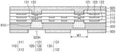
图3是示出印刷电路板的示例的截面图。FIG. 3 is a cross-sectional view showing an example of a printed circuit board.
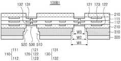
参照图3,根据示例的印刷电路板100A1包括:多个绝缘层110;多个电路层120,设置在多个绝缘层110的内部和外部中的至少一者上;多个过孔层130,穿透多个绝缘层110的至少一部分并连接多个电路层120之间的空间;第一钝化层210,设置在多个绝缘层110的一个表面和另一表面上;以及增强层300,设置在多个绝缘层110的一个表面上并且具有第一开口510和第二开口520,第一开口510具有第一宽度W1,第二开口520具有不同于第一宽度W1的第二宽度W2。Referring to FIG. 3 , a printed circuit board 100A1 according to an example includes: a plurality of
例如,在根据示例的印刷电路板100A1中,如在稍后将描述的工艺中,增强层300堆叠在多个绝缘层110的一个表面上,并且可增强印刷电路板100A1的刚度,这有利于控制印刷电路板100A1的翘曲。For example, in the printed circuit board 100A1 according to the example, as in a process to be described later, the
此外,根据示例的印刷电路板100A1可使用稍后将描述的分离载体膜(DCF)来制造。因此,多个电路层120中的第一电路层121可嵌入印刷电路板100A1的另一表面中。因此,可将第一电路层121实现为更精细的电路层。因此,可使第一电路层121的电路图案之间的节距和线宽小于常规电路层的节距和线宽,其中,节距可指将相邻电路图案的中心彼此连接的最短距离的平均值,并且线宽可指电路图案的水平宽度的平均值。In addition, the printed circuit board 100A1 according to the example may be manufactured using a separation carrier film (DCF) which will be described later. Accordingly, the
此外,根据示例,可在印刷电路板100A1的增强层300中形成具有不同宽度的开口。例如,可形成具有第一宽度W1的第一开口510和具有第二宽度W2的第二开口520,并且由于第一开口510和第二开口520的宽度不同,因此增强层300的内壁可具有台阶。由于第一开口510和第二开口520的宽度彼此不同,因此当稍后将描述的电连接金属设置在第一开口510和第二开口520中时,可进一步增强可靠性和粘附性。Also, according to an example, openings having different widths may be formed in the
在下文中,将参照附图更详细地描述根据示例的印刷电路板100A1的组件。Hereinafter, components of the printed circuit board 100A1 according to the example will be described in more detail with reference to the accompanying drawings.
多个绝缘层110包括顺序地堆叠的第一绝缘层111和第二绝缘层112。可使用绝缘材料作为多个绝缘层110的材料,并且可使用诸如环氧树脂的热固性树脂或诸如聚酰亚胺树脂的热塑性树脂作为绝缘材料。The plurality of insulating
此外,可使用在热固性树脂或热塑性树脂中包含无机填料(诸如二氧化硅)和增强材料(诸如玻璃纤维)的材料作为绝缘材料。例如,可使用半固化片,但不限于此,并且可使用不包含诸如玻璃纤维的增强材料的材料,即在热固性树脂或热塑性树脂中包含无机填料(诸如二氧化硅)的材料,例如,味之素堆积膜(Ajinomoto Build-up Film,ABF)等。ABF可以以树脂涂覆铜(RCC)的形式提供,但不限于此。如果需要,可使用诸如PID(感光电介质)的感光材料。在图3的情况下,仅示出了第一绝缘层111和第二绝缘层112,但是多个绝缘层110可根据需要和设计包括更多数量的绝缘层。In addition, a material containing an inorganic filler such as silica and a reinforcing material such as glass fiber in a thermosetting resin or a thermoplastic resin may be used as the insulating material. For example, a prepreg can be used, but not limited thereto, and a material that does not contain a reinforcing material such as glass fiber, that is, a material that contains an inorganic filler such as silica in a thermosetting resin or a thermoplastic resin, for example, Ajinomoto Build-up film (Ajinomoto Build-up Film, ABF) and the like. ABF can be provided in the form of resin coated copper (RCC), but is not limited to this. A photosensitive material such as PID (Photosensitive Dielectric) may be used if necessary. In the case of FIG. 3 , only the first insulating
多个电路层120可设置在多个绝缘层110的内部和外部中的至少一者上。多个电路层120可包括从多个绝缘层110的一个表面突出的第二电路层122、从多个绝缘层110的另一表面嵌入的第一电路层121以及设置在多个绝缘层110内部的内电路层123。以图3的印刷电路板100A1为例,多个电路层120可包括嵌入第一绝缘层111的上表面中的第一电路层121、嵌入第二绝缘层112的上表面中的内电路层123、以及设置成在第二绝缘层112的下表面上突出的第二电路层122。作为多个电路层120的材料,可使用金属材料。作为金属材料,可使用铜(Cu)、铝(Al)、银(Ag)、锡(Sn)、金(Au)、镍(Ni)、铅(Pb)、钛(Ti)或它们的合金。多个电路层120可根据设计执行各种功能。例如,多个电路层120可包括接地图案、电力图案、信号图案等。这些图案中的每个可具有线、面或焊盘形状。多个电路层120可通过镀覆工艺(诸如,加成工艺(AP)、半AP(SAP)、改进的SAP(MSAP)、封孔(TT)等)形成,并且因此可包括种子层(无电镀层)和基于种子层形成的电解镀层。当以RCC形式提供多个绝缘层110时,多个电路层120还可包括诸如铜箔的金属箔,并且如果需要,可在金属箔的表面上存在底漆树脂。在图3的情况下,仅示出了第一电路层121和第二电路层122以及内电路层123,但是多个电路层120可根据需要和设计包括更多数量的电路层。在这种情况下,内电路层123可包括更多数量的电路层。The plurality of circuit layers 120 may be disposed on at least one of inside and outside of the plurality of insulating
多个过孔层130可包括穿透第一绝缘层111并使第一电路层121和内电路层123电连接的第一过孔层131,以及穿透第二绝缘层112并使内电路层123和第二电路层122电连接的第二过孔层132。作为多个过孔层130的材料,可使用金属材料。作为金属材料,可使用铜(Cu)、铝(Al)、银(Ag)、锡(Sn)、金(Au)、镍(Ni)、铅(Pb)、钛(Ti)或它们的合金。根据设计,多个过孔层130可包括信号过孔、接地过孔、电力过孔等。多个过孔层130的各个过孔可通过使用金属材料完全填充通路孔来形成,或者可使用金属材料沿着通路孔的壁表面形成。多个过孔层130也可通过镀覆工艺(诸如,加成工艺(AP)、半AP(SAP)、改进的SAP(MSAP)、封孔(TT)等)形成,并且因此可包括种子层(无电镀层)和基于种子层形成的电解镀层。多个过孔层130的各个过孔可具有其中一个表面的宽度大于另一表面的宽度的锥形形状。具体地,多个过孔层130中的各个过孔可具有其宽度在从多个绝缘层110的一个表面(例如,下表面)到另一表面(例如,上表面)的方向上变窄的锥形形状。在图3的情况下,仅示出了第一过孔层131和第二过孔层132,但是根据设计的必要性,多个过孔层130可包括更多数量的过孔层。The plurality of via
第一钝化层210可保护内部构造免受外部物理和化学损坏等。第一钝化层210可设置在多个绝缘层110的一个表面和另一表面上,并且可分别具有多个第三开口530。第三开口530可形成在其至少一部分与稍后将描述的增强层300的第一开口510和第二开口520在堆叠方向上重叠的位置,并且可向外暴露最外面的电路层。例如,设置在多个绝缘层110的一个表面上的第一钝化层210的第三开口530可向外暴露第二电路层122的至少一部分,并且设置在多个绝缘层110的另一表面上的第一钝化层210的第三开口530可向外暴露第一电路层121的至少一部分。The
第一钝化层210的第三开口530的宽度可大于或小于第一电路层121和第二电路层122(其至少一部分暴露于第三开口530)的线宽。参照图3的实施例,公开了其中第三开口530的宽度与第一电路层121和第二电路层122的线宽相同的结构,但是第三开口530的宽度可小于第一电路层121和第二电路层122中的每个的线宽,或者可大于第一电路层121和第二电路层122中的每个的线宽。The width of the
作为第一钝化层210的材料,可使用绝缘材料。在这种情况下,作为绝缘材料,可使用诸如环氧树脂的热固性树脂、诸如聚酰亚胺树脂的热塑性树脂,或者可使用其中热固性树脂或热塑性树脂与无机填料混合的材料,例如,ABF,但不限于此。可使用诸如感光电介质(PID)的感光绝缘材料。As a material of the
尽管未示出,但是表面处理层可设置在第一电路层121和第二电路层122的由第一钝化层210的第三开口530暴露的区域中。通过表面处理层,可防止由第三开口530暴露的第一电路层121和第二电路层122的氧化,并且可确保稍后设置的电连接金属的可靠性。作为表面处理层,可使用镍(Ni)镀层、金(Au)镀层或有机可焊性保护(OSP)表面处理层,但不限于此。Although not shown, a surface treatment layer may be disposed in regions of the
增强层300可执行加强印刷电路板100A1的刚性的功能。增强层300可设置在多个绝缘层110的一个表面上,例如,可设置于设置在多个绝缘层110的一个表面上的第一钝化层210上。增强层300需要具有一定的厚度,以便确保印刷电路板100A1的刚性。因此,增强层300可比多个绝缘层110中的第一绝缘层111和第二绝缘层112中的每个厚。另外,增强层300可比第一钝化层210厚。The reinforcing
第一开口510和第二开口520可形成在增强层300中。第一开口510和第二开口520可通过稍后描述的喷砂工艺(blast process)形成,并且可形成为分别具有第一宽度W1和第二宽度W2。第一开口510的第一宽度W1可表示第一开口510在垂直于堆叠方向的截面中的宽度。在本公开中,当其截面是圆形时,宽度可表示圆的直径,当其截面是正方形时,宽度可表示一条边的长度,并且当其截面是矩形时,宽度可表示每条边的长度的平均值。The
第一宽度W1可大于第二宽度W2。另外,与形成在上述第一钝化层210中的第三开口530的第三宽度W3相比,第二宽度W2可大于第三宽度W3。结果,第一宽度W1可大于第二宽度W2,并且第二宽度W2可大于第三宽度W3。由于第二宽度W2大于第三宽度W3,因此当稍后将电连接金属设置在第三开口530中时,可提高电连接金属的可靠性和粘附性,并且可防止剥离现象。另外,由于第一宽度W1大于第二宽度W2,因此与之类似,可提高电连接金属的可靠性和粘附性,并且可防止剥离现象。The first width W1 may be greater than the second width W2. In addition, the second width W2 may be greater than the third width W3 compared to the third width W3 of the
第一开口510和第二开口520可形成为彼此连接,并且其至少一些区域可在堆叠方向上彼此重叠。另外,由于第一宽度W1可大于第二宽度W2,因此参照图3所示的实施例,当从印刷电路板100A1的堆叠方向观察时,第二开口520可形成在第一开口510中。因此,由于第一开口510和第二开口520具有不同的第一宽度W1和第二宽度W2,增强层300的内壁可具有台阶。由于增强层300的内壁具有台阶,因此可进一步提高设置在第一开口510和第二开口520中的电连接金属的粘附性,并且还可提高可靠性。The
此外,第三开口530也可形成为连接到第二开口520,并且其至少一些区域可在堆叠方向上重叠。参照图3所示的实施例,在堆叠方向上,第一开口510可包括第二开口520和第三开口530两者,并且第一开口510、第二开口520和第三开口530可彼此连接并一体形成。In addition, the
绝缘材料可用作增强层300的材料,并且诸如环氧树脂的热固性树脂或诸如聚酰亚胺树脂的热塑性树脂可用作绝缘材料。增强层300的材料可包括绝缘材料,并且也可使用不包括诸如玻璃纤维等的增强材料的材料,即在热固性树脂或热塑性树脂中包含无机填料(诸如二氧化硅)的材料,例如,ABF等。ABF可以以RCC的形式提供,但不限于此。根据需要,可使用诸如PID的感光绝缘材料。另外,在增强层300的情况下,为了确保印刷电路板100A1的刚性,增强层300可包括具有比多个绝缘层110和第一钝化层210的刚性更大的刚性的材料,因此,增强层300可具有比多个绝缘层110和第一钝化层210相对更大的刚性。An insulating material may be used as a material of the
图4是示意性地示出图3的印刷电路板的变型示例的截面图。FIG. 4 is a cross-sectional view schematically showing a modified example of the printed circuit board of FIG. 3 .
参照图4,在根据变型示例的印刷电路板100A2中,与根据上述示例的印刷电路板100A1相比,第二钝化层220可进一步设置在增强层300上。在这种情况下,可在第二钝化层220中形成具有第四宽度W4的多个第四开口540。Referring to FIG. 4 , in a printed circuit board 100A2 according to a modified example, a
具体地,可在第二钝化层220中形成具有第四宽度W4的多个第四开口540,并且第四开口540的至少一部分可形成为在堆叠方向上与第一开口510、第二开口520和第三开口530中的每个重叠。参照图4所示的实施例,第四开口540可连接到第一开口510,并且当从堆叠方向观察时,第四开口540包括第一开口510、第二开口520和第三开口530中的全部。也就是说,第一开口510、第二开口520、第三开口530和第四开口540可彼此连接成一体。Specifically, a plurality of
作为第二钝化层220的材料,可使用用作第一钝化层210的材料的绝缘材料,但是第一钝化层210和第二钝化层220的材料不必相同。As a material of the
当设置第二钝化层220时,示出了其中第一钝化层210、增强层300和第二钝化层220顺序堆叠在印刷电路板100A2的多个绝缘层110的一侧上的结构。由此,在印刷电路板100A2的外表面之中,设置有电连接金属的一侧(是设置有稍后将描述的电子组件的一侧的相对侧)的刚性可被进一步增强。通过这种结构,在本公开中,与其中增强层设置在设置有电子组件的一侧上的结构相比,能够在结构上减薄。这是因为增强层300和第二钝化层220可设置在最初用于待设置电连接金属的基板之间的间隙中。When the
关于其他重复构造的描述,根据示例的印刷电路板100A1的描述可同样适用,因此将省略。Regarding the description of other repetitive configurations, the description of the printed circuit board 100A1 according to the example is equally applicable and thus will be omitted.
图5是示意性地示出图3的印刷电路板的另一变型示例的截面图。FIG. 5 is a cross-sectional view schematically showing another modified example of the printed circuit board of FIG. 3 .
参照图5,在根据另一变型示例的印刷电路板100A3中,与根据上述变型示例的印刷电路板100A2相比,金属层400可进一步设置在增强层300上。在这种情况下,金属层400可被第二钝化层220覆盖。Referring to FIG. 5 , in a printed circuit board 100A3 according to another modified example, a
具体地,金属层400可设置在增强层300的和增强层300与第一钝化层210接触的表面相对的表面上,并且可被第二钝化层220覆盖。金属层400可被图案化为暴露第四开口540来形成第四开口540。Specifically, the
金属层400可设置在增强层300上以进一步增强印刷电路板100A3的刚性,从而有效地控制翘曲。当以RCC的形式提供增强层300时,可通过蚀刻包括在RCC中的铜箔层来使金属层400图案化,但不限于此。A
可使用金属材料作为金属层400的材料,并且作为金属材料,可使用铜(Cu)、铝(Al)、银(Ag)、锡(Sn)、金(Au)、镍(Ni)、铅(Pb)、钛(Ti)或它们的合金。A metal material can be used as the material of the
另外,金属层400可相对地设置在印刷电路板100A3的外侧并连接到印刷电路板100A3的地以执行EMI(电磁干扰)屏蔽功能。In addition, the
关于其他重复组件的描述,根据变型示例的印刷电路板100A2的描述可同样适用,因此将省略其描述。Regarding the description of other overlapping components, the description of the printed circuit board 100A2 according to the modification example is equally applicable, and thus description thereof will be omitted.
图6是示意性地示出图3的印刷电路板的另一变型示例的截面图。FIG. 6 is a cross-sectional view schematically showing another modified example of the printed circuit board of FIG. 3 .
参照图6,在根据另一变型示例的印刷电路板100A4中,与根据上述另一变型示例的印刷电路板100A3相比,可进一步设置电子组件600以及第一电连接金属710和第二电连接金属720。Referring to FIG. 6 , in a printed circuit board 100A4 according to another modification example, compared with the printed circuit board 100A3 according to another modification example described above, an
具体地,电子组件600可设置在印刷电路板100A4的另一侧上。参照图6的实施例,电子组件600可设置在多个绝缘层110的另一表面上,具体地,可设置于设置在多个绝缘层110的另一表面上的第一钝化层210上。在这种情况下,诸如芯片附着膜(DAF)的粘合层可设置在电子组件600和第一钝化层210之间以保持粘合力,但不限于此,并且电子组件600也可设置成在没有单独的粘合层的情况下与第一钝化层210接触。Specifically, the
电子组件600可以是其中数百到数百万个或以上的元件集成在单个芯片中的集成电路(IC)裸片。例如,电子组件600可以是诸如中央处理器(例如,CPU)、图形处理器(例如,GPU)、现场可编程门阵列(FPGA)、数字信号处理器、密码处理器、微处理器、微控制器等的处理器芯片,具体地,应用处理器(AP),但不限于此,并且可以是诸如易失性存储器(例如,DRAM)、非易失性存储器(例如,ROM)、闪存等的存储器芯片,或者是诸如模数转换器或专用IC(ASIC)等的逻辑芯片。如果需要,电子组件600可以是片式无源组件,例如,片式电感器、片式电容器等。电子组件600可被设置为使得其上设置有连接焊盘120P的表面面向上,并且与其上设置有连接焊盘120P的表面相对的表面面向下。电子组件600的连接焊盘120P可包括诸如铜(Cu)或铝(Al)的金属材料,并且可连接到第一电路层121。
第一电连接金属710可设置在印刷电路板100A4的一侧上。具体地,第一电连接金属710可设置于设置在多个绝缘层110的一个表面上的第一钝化层210上,并且可设置成填充上述第一开口510、第二开口520、第三开口530和第四开口540中的每个的至少一部分。第一电连接金属710可电连接到暴露的第二电路层122。第一电连接金属710可将印刷电路板100A4物理连接和/或电连接到外部实体。例如,印刷电路板100A4可通过第一电连接金属710安装在电子装置的主板、其他BGA基板等上。第一电连接金属710可将印刷电路板100A4物理连接和/或电连接到表面安装在其上的组件,并且可将印刷电路板100A4连接到印刷电路板100A4安装在其上的其他基板,诸如主板等。第一电连接金属710可利用锡(Sn)或含锡(Sn)的合金(例如,焊料)形成,但不限于此。第一电连接金属710可以是焊盘、焊球、引脚等。The first
由于第一电连接金属710设置在彼此具有不同宽度的第一开口510、第二开口520、第三开口530和第四开口540中,因此可进一步提高结合力和可靠性。换句话说,由于第一钝化层210、增强层300和第二钝化层220中的每个的内壁具有不同的宽度,因此内壁形成台阶。与具有平滑内壁的正常开口相比,内壁中具有台阶的开口可通过锚固效应等增加电连接金属和绝缘层之间的结合力。Since the first
因此,一体形成的彼此连接的第一开口510、第二开口520、第三开口530和第四开口540可形成在印刷电路板100A4的一侧上,并且第一电连接金属710可设置在第一开口510、第二开口520、第三开口530和第四开口540中,使得可提高内壁和第一电连接金属710之间的结合力和可靠性,以有效地改善第一电连接金属710剥离的现象。Therefore, the
第二电连接金属720可将电子组件600电连接到第一电路层121。第二电连接金属720可利用锡(Sn)或含锡(Sn)的合金(例如,与第一电连接金属710的焊料类似的焊料)形成,但不限于此。第二电连接金属720可以是焊盘、焊球、引脚等,并且可以是参照图6中所示的实施例的金属线。因此,电子组件600和第一电路层121可通过引线键合连接。The second
关于其他重复组件的描述,根据上述其他变型示例的印刷电路板100A3的描述可同样适用,因此将省略其描述。Regarding the description of other repetitive components, the description of the printed circuit board 100A3 according to the above-mentioned other modified example is equally applicable, and thus description thereof will be omitted.
图7是示意性地示出印刷电路板的另一示例的截面图。Fig. 7 is a cross-sectional view schematically showing another example of a printed circuit board.
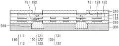
参照图7,在根据另一示例的印刷电路板100B1中,与根据上述示例的印刷电路板100A1相比,增强层300可包括多个层。Referring to FIG. 7 , in a printed circuit board 100B1 according to another example, the
具体地,参照图7的实施例,增强层可包括第一增强层310和设置在第一增强层310上的第二增强层320。如在本实施例中,由于增强层具有多个层,因此能够更有效地确保印刷电路板100B1的刚性。Specifically, referring to the embodiment of FIG. 7 , the enhancement layer may include a
关于第一增强层310,根据上述示例的印刷电路板100A1中的增强层300的描述可同样适用。With regard to the
根据本实施例,第一增强层310的第一开口510也可形成在第二增强层320中。也就是说,第一开口510可通过稍后描述的喷砂工艺共同形成在第一增强层310和第二增强层320中。因此,形成在第一增强层310和第二增强层320中的每个中的第一开口510可连接并且具有基本相同的宽度。在本公开中,基本相同是指:不仅包括物理上/数值上完全相同的情况,而且包括在工艺期间可能发生的误差。According to this embodiment, the
第二增强层320可堆叠在第一增强层310上,并且第二增强层320的材料可包括与上述第一增强层310的材料相同的材料。然而,不是必然包括与第一增强层310相同的材料。The
关于其他重复组件的描述,根据上述示例的印刷电路板100A1的描述可同样适用,因此将省略其描述。Regarding the description of other repetitive components, the description of the printed circuit board 100A1 according to the above-mentioned example is equally applicable, and thus a description thereof will be omitted.
图8是示意性地示出图7的印刷电路板的变型示例的截面图。FIG. 8 is a cross-sectional view schematically showing a modified example of the printed circuit board of FIG. 7 .
参照图8,在根据变型示例的印刷电路板100B2中,与根据上述另一示例的印刷电路板100B1相比,第二钝化层220可进一步设置在第二增强层320上。在这种情况下,可在第二钝化层220中形成具有第四宽度W4的多个第四开口540。Referring to FIG. 8 , in a printed circuit board 100B2 according to a modified example, a
具体地,具有第四开口540的第二钝化层220可设置在第二增强层320上,第四开口540具有第四宽度W4,并且当从堆叠方向观察时,第四开口540可形成为与第一开口510、第二开口520和第三开口530中的每个重叠。Specifically, the
关于第二钝化层220、第四开口540和第四宽度W4,可按原样应用与上述相同的描述。Regarding the
关于其他重复组件的描述,根据另一示例的印刷电路板100B1的描述可同样适用,因此将省略其描述。Regarding the description of other repetitive components, the description of the printed circuit board 100B1 according to another example is equally applicable, and thus the description thereof will be omitted.
图9是示意性地示出图7的印刷电路板的另一变型示例的截面图。FIG. 9 is a cross-sectional view schematically showing another modified example of the printed circuit board of FIG. 7 .
参照图9,在根据另一变型示例的印刷电路板100B3中,与根据上述变型示例的印刷电路板100B2相比,多个第一金属层410和多个第二金属层420可分别设置在第一增强层310和第二增强层320上。在这种情况下,第一金属层410可被第二增强层320覆盖,并且第二金属层420可被第二钝化层220覆盖。Referring to FIG. 9 , in a printed circuit board 100B3 according to another modified example, compared with the printed circuit board 100B2 according to the above-described modified example, a plurality of
第一金属层410和第二金属层420可分别执行附加地增强印刷电路板100B3的刚性的功能,并且可附加地连接到地以执行EMI屏蔽功能。The
关于第一金属层410和第二金属层420的材料和性质,根据上述另一变型示例的印刷电路板100A3中的金属层400的描述可同样适用。With regard to the materials and properties of the
关于其他重复组件的描述,根据变型示例的印刷电路板100B2的描述可同样适用,因此将省略其描述。Regarding the description of other overlapping components, the description of the printed circuit board 100B2 according to the modified example is equally applicable, and thus description thereof will be omitted.
图10是示意性地示出图7的印刷电路板的另一变型示例的截面图。FIG. 10 is a cross-sectional view schematically showing another modified example of the printed circuit board of FIG. 7 .
参照图10,在根据另一变型示例的印刷电路板100B4中,与根据上述另一变型示例的印刷电路板100B3相比,还设置有电子组件600以及第一电连接金属710和第二电连接金属720。Referring to FIG. 10 , in a printed circuit board 100B4 according to another modification example, compared with the printed circuit board 100B3 according to another modification example described above, an
关于电子组件600以及第一电连接金属710和第二电连接金属720,根据上述另一变型示例的印刷电路板100A4的描述可同样适用,因此省略其详细描述。Regarding the
关于其他重复组件的描述,根据上述其他变型示例的印刷电路板100B3的描述可同样适用,因此将省略其描述。Regarding the description of other repetitive components, the description of the printed circuit board 100B3 according to the above-mentioned other modified example is equally applicable, and thus description thereof will be omitted.
图11至图17是示意性地示出制造图3的印刷电路板的示例的截面图。11 to 17 are cross-sectional views schematically showing an example of manufacturing the printed circuit board of FIG. 3 .
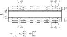
参照图11和图12,首先,制备其中在至少一个表面上设置有金属箔821和822的载体800。此后,通过镀覆工艺在金属箔821和822上形成第一电路层121。接下来,在第一电路层121上形成用于覆盖第一电路层121的第一绝缘层111,并使用激光钻孔等在第一绝缘层111中加工通路孔,然后通过镀覆工艺形成第一过孔层131和内电路层123。接下来,形成包埋内电路层123的第二绝缘层112,使用激光钻孔等在第二绝缘层112中加工通路孔,然后通过镀覆工艺形成第二过孔层132和第二电路层122。接下来,形成具有使第二电路层122的至少一部分暴露的第四开口540的第一钝化层210。Referring to FIGS. 11 and 12 , first, a
参照图13,在第一钝化层210上形成覆盖从第一钝化层210暴露的第二电路层122的第一保护层910。Referring to FIG. 13 , a
第一保护层910可用于在稍后将描述的喷砂工艺期间保护第二电路层122,并且可具有与稍后将形成的第二开口520的宽度相同的第二宽度W2。可不受限制地使用第一保护层910,只要其包括在喷砂过程中受影响较小的材料即可。例如,可使用已知的干膜抗蚀剂,并且还可包括可通过化学处理熔化的树脂。可选地,第一保护层910可根据需要包括金属材料。The first
参照图14,可在第一钝化层210上形成填充并覆盖第一保护层910的增强层300。当增强层300以RCC的形式提供时,可另外设置铜箔M。增强层300可不包括诸如玻璃纤维的增强材料,因为其一部分通过稍后描述的喷砂工艺去除。Referring to FIG. 14 , a
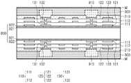
参照图15,在分离载体800的两个表面上的层叠体中的每个后,可在多个绝缘层110的另一侧上设置具有开口的第一钝化层210。设置在多个绝缘层110的另一侧上的第一钝化层210可向外暴露嵌入第一绝缘层111中的第一电路层121的上表面。Referring to FIG. 15 , after separating each of the laminates on both surfaces of the
另外,当增强层300以RCC的形式提供时,可蚀刻并去除铜箔M。然而,铜箔M不一定必须被完全去除,并且铜箔M可仅在部分区域中被图案化并去除,并且可保留在剩余区域中,并且剩余区域中的铜箔可增强印刷电路板的刚性,如先前描述的图5所示。In addition, when the
参照图16,可在层叠体的两个表面上堆叠第二保护层920。由于第二保护层920可用作用于喷砂工艺的掩模,因此它可包括受喷砂工艺影响较小的材料。在这种情况下,可选择性地去除第二保护层920中与增强层300接触的第二保护层920的一部分。开口920h可存在于第二保护层920被选择性地去除的区域中,并且第二保护层920可彼此间隔开开口920h的宽度。开口920h的宽度可与第一宽度W1基本相同,第一宽度W1是稍后在增强层300中形成的第一开口510的宽度。另外,当在堆叠方向上观察时,开口920h的截面可与稍后形成的形成在增强层300中的第一开口510的截面基本相同。Referring to FIG. 16 , a second
图17示出了使用第二保护层920作为掩模的喷砂工艺的结果(根据图3的本公开的示例的印刷电路板100A1的结构)。在使用第二保护层920作为掩模通过喷砂工艺在增强层300中形成第一开口510之后,可去除第一保护层910,使得可形成第二开口520。当第一保护层910包括诸如干膜的感光材料时,可通过曝光/显影工艺将其去除,但不限于此。也就是说,当第一保护层910包括与特定化学品反应的树脂时,可通过化学处理去除第一保护层910而无需曝光/显影工艺。可选地,当第一保护层910包括金属材料时,也可通过使用与第一保护层910反应的蚀刻剂进行蚀刻来去除第一保护层910。在这种情况下,上述表面处理层可设置在第二电路层122上,并且由于表面处理层的保护,可仅去除第一保护层910而不损坏第二电路层122。FIG. 17 shows the result of the sandblasting process using the second
如上所述,当在存在第一保护层910的状态下对增强层300执行喷砂工艺时,与喷砂工艺直接影响电路层(例如,第二电路层122)的情况相比,可防止对第二电路层122的损坏,并且可减小第二电路层122的厚度,使得防止发生信号传输故障。As described above, when the sandblasting process is performed on the
如在此使用的,空间相对术语“侧部”、“侧表面”等用于指代在第一方向(例如,相对于图3的截面的向左方向)或第二方向(例如,相对于图3的截面的向右方向)上的部分或者在所述方向上的表面。空间相对术语“上侧”、“上部”、“上表面”等用于指代在与第一方向和第二方向垂直的第三方向上的部分或者在所述方向上的表面,而空间相对术语“下侧”、“下部”、“下表面”等用于指代在与第三方向相反的方向上的部分或者在所述方向上的表面。另外,所述空间相对术语已被用作包括目标组件定位在对应方向上但不直接接触参考组件的情况以及目标组件在相应方向上直接接触参考组件的情况的概念。然而,为了便于描述,这些术语可如上定义,并且示例性实施例的范围不特别限于上述术语。As used herein, the spatially relative terms "side", "side surface" and the like are used to refer to a direction in a first direction (e.g., a leftward direction with respect to the cross-section of FIG. 3 ) or a second direction (e.g., with respect to The part on the rightward direction of the cross-section of FIG. 3 ) or the surface in said direction. The spatially relative terms "upper side", "upper", "upper surface" and the like are used to refer to a portion in a third direction perpendicular to the first direction and the second direction or a surface in said direction, while the spatially relative term "Lower side", "lower part", "lower surface" and the like are used to refer to a portion in the direction opposite to the third direction or a surface in the direction. In addition, the spatially relative term has been used as a concept including a case where a target component is positioned in a corresponding direction but does not directly contact a reference component, and a case where a target component directly touches a reference component in a corresponding direction. However, these terms may be defined as above for convenience of description, and the scope of exemplary embodiments is not particularly limited to the above terms.
如在此使用的,术语“连接”不仅可指“直接连接”,而且还可包括借助于粘合层等的“间接连接”。术语“电连接”可包括构成元件“物理连接”的情况和构成元件“非物理连接”的情况两者。此外,术语“第一”、“第二”等可用于将一个构成元件与另一个构成元件区分开,并且可不限制与构成元件相关的顺序和/或重要性等。在一些情况下,在不脱离示例性实施例的范围的情况下,第一构成元件可被称为第二构成元件,并且类似地,第二构成元件可被称为第一构成元件。As used herein, the term "connection" may mean not only "direct connection" but also "indirect connection" via an adhesive layer or the like. The term "electrically connected" may include both the case where constituent elements are "physically connected" and the case where constituent elements are "not physically connected". Also, the terms 'first', 'second', etc. may be used to distinguish one constituent element from another, and may not limit the order and/or importance, etc., related to the constituent elements. In some cases, without departing from the scope of exemplary embodiments, a first constituent element may be referred to as a second constituent element, and, similarly, a second constituent element may be referred to as a first constituent element.
如在此使用的,术语“实施例”被提供以强调特定的特征、结构或特性,并且不必然指代相同的实施例。此外,特定特性或特征可在一个或更多个实施例中以任意合适的方式组合。例如,除非被描述为与其他实施例中的特征相反或不一致,否则即使在其他实施例中没有描述,在特定示例性实施例中描述的特征也可用于其他实施例中。As used herein, the term "embodiment" is provided to emphasize a particular feature, structure or characteristic and does not necessarily refer to the same embodiment. Furthermore, the particular features or characteristics may be combined in any suitable manner in one or more embodiments. For example, features described in a particular exemplary embodiment can be used in other embodiments even if not described in other embodiments, unless described as contrary to or inconsistent with features in other embodiments.
在此使用的术语仅描述特定实施例,并且本公开不限于此。如在此使用的,除非上下文另有明确说明,否则单数形式旨在也包括复数形式。The terms used herein describe specific embodiments only, and the present disclosure is not limited thereto. As used herein, the singular forms are intended to include the plural unless the context clearly dictates otherwise.
如上所述,作为本公开的各种效果之一,可提供一种具有增强刚度的印刷电路板。As described above, as one of various effects of the present disclosure, a printed circuit board having enhanced rigidity can be provided.
作为本公开的各种效果中的另一效果,可提供一种包括其中形成具有不同宽度的多个开口的增强层的印刷电路板。As another effect among the various effects of the present disclosure, there may be provided a printed circuit board including a reinforcement layer in which a plurality of openings having different widths are formed.
作为本公开的若干效果中的另一效果,可提供一种堆叠有多个增强层的印刷电路板。As another effect among the effects of the present disclosure, there may be provided a printed circuit board in which a plurality of reinforcement layers are stacked.
虽然上面已经示出和描述了示例性实施例,但是对于本领域技术人员将易于理解的是,可在不脱离由所附权利要求限定的本公开的范围的情况下做出修改和变型。While exemplary embodiments have been shown and described above, it will be readily apparent to those skilled in the art that modifications and variations can be made without departing from the scope of the present disclosure as defined in the appended claims.
Claims (20)
Applications Claiming Priority (2)
| Application Number | Priority Date | Filing Date | Title |
|---|---|---|---|
| KR10-2021-0058672 | 2021-05-06 | ||
| KR1020210058672AKR20220151431A (en) | 2021-05-06 | 2021-05-06 | Printed circuit board |
Publications (1)
| Publication Number | Publication Date |
|---|---|
| CN115315061Atrue CN115315061A (en) | 2022-11-08 |
Family
ID=83853673
Family Applications (1)
| Application Number | Title | Priority Date | Filing Date |
|---|---|---|---|
| CN202111318642.2APendingCN115315061A (en) | 2021-05-06 | 2021-11-09 | Printed circuit board |
Country Status (3)
| Country | Link |
|---|---|
| US (1) | US11882652B2 (en) |
| KR (1) | KR20220151431A (en) |
| CN (1) | CN115315061A (en) |
Families Citing this family (1)
| Publication number | Priority date | Publication date | Assignee | Title |
|---|---|---|---|---|
| CN116158200A (en)* | 2021-06-17 | 2023-05-23 | 庆鼎精密电子(淮安)有限公司 | Circuit board assembly and manufacturing method thereof |
Citations (10)
| Publication number | Priority date | Publication date | Assignee | Title |
|---|---|---|---|---|
| US5227013A (en)* | 1991-07-25 | 1993-07-13 | Microelectronics And Computer Technology Corporation | Forming via holes in a multilevel substrate in a single step |
| US20020111009A1 (en)* | 2001-02-15 | 2002-08-15 | Megic Corporation | Reliable metal bumps on top of I/O pads after removal of test probe marks |
| JP2004259714A (en)* | 2003-02-24 | 2004-09-16 | Murata Mfg Co Ltd | Electronic component comprising multilayer ceramic substrate and its producing method |
| US20060097370A1 (en)* | 2004-10-21 | 2006-05-11 | International Business Machines Corporation | Stepped integrated circuit packaging and mounting |
| US20090065245A1 (en)* | 2006-11-13 | 2009-03-12 | Phoenix Precision Technology Corporation | Circuit board structure and fabrication method thereof |
| US20170253975A1 (en)* | 2014-09-17 | 2017-09-07 | C. Uyemura & Co., Ltd. | Method for manufacturing wiring substrate and wiring substrate manufactured thereby |
| US20180096941A1 (en)* | 2016-09-30 | 2018-04-05 | Samsung Electro-Mechanics Co., Ltd. | Fan-out semiconductor package |
| JP2019121765A (en)* | 2018-01-11 | 2019-07-22 | イビデン株式会社 | Printed wiring board and manufacturing method thereof |
| JP2019121764A (en)* | 2018-01-11 | 2019-07-22 | イビデン株式会社 | Wiring board and manufacturing method thereof |
| JP2020031091A (en)* | 2018-08-21 | 2020-02-27 | イビデン株式会社 | Printed wiring board |
Family Cites Families (11)
| Publication number | Priority date | Publication date | Assignee | Title |
|---|---|---|---|---|
| JPWO2009104506A1 (en)* | 2008-02-19 | 2011-06-23 | 日本電気株式会社 | Printed wiring board, electronic device and manufacturing method thereof |
| JP5281346B2 (en) | 2008-09-18 | 2013-09-04 | 新光電気工業株式会社 | Semiconductor device and manufacturing method thereof |
| JP5715835B2 (en) | 2011-01-25 | 2015-05-13 | 新光電気工業株式会社 | Semiconductor package and manufacturing method thereof |
| JP5990421B2 (en)* | 2012-07-20 | 2016-09-14 | 新光電気工業株式会社 | Wiring substrate, manufacturing method thereof, and semiconductor package |
| US9679865B2 (en)* | 2013-11-08 | 2017-06-13 | SK Hynix Inc. | Substrate for semiconductor package and semiconductor package having the same |
| US9997442B1 (en)* | 2016-12-14 | 2018-06-12 | Advanced Semiconductor Engineering, Inc. | Semiconductor device and method of manufacturing the same |
| US10854550B2 (en)* | 2017-09-28 | 2020-12-01 | Advanced Semiconductor Engineering, Inc. | Semiconductor package and method of manufacturing the same |
| KR102450598B1 (en) | 2017-11-09 | 2022-10-07 | 삼성전기주식회사 | Support attached printed circuit board and manufacturing method thereof |
| JP7221601B2 (en)* | 2018-06-11 | 2023-02-14 | 新光電気工業株式会社 | Wiring board, method for manufacturing wiring board |
| KR20200051215A (en)* | 2018-11-05 | 2020-05-13 | 삼성전기주식회사 | Printed circuit board and package structure having the same |
| KR102710005B1 (en)* | 2019-10-21 | 2024-09-26 | 엘지이노텍 주식회사 | Circuit board |
- 2021
- 2021-05-06KRKR1020210058672Apatent/KR20220151431A/enactivePending
- 2021-08-27USUS17/459,212patent/US11882652B2/enactiveActive
- 2021-11-09CNCN202111318642.2Apatent/CN115315061A/enactivePending
Patent Citations (10)
| Publication number | Priority date | Publication date | Assignee | Title |
|---|---|---|---|---|
| US5227013A (en)* | 1991-07-25 | 1993-07-13 | Microelectronics And Computer Technology Corporation | Forming via holes in a multilevel substrate in a single step |
| US20020111009A1 (en)* | 2001-02-15 | 2002-08-15 | Megic Corporation | Reliable metal bumps on top of I/O pads after removal of test probe marks |
| JP2004259714A (en)* | 2003-02-24 | 2004-09-16 | Murata Mfg Co Ltd | Electronic component comprising multilayer ceramic substrate and its producing method |
| US20060097370A1 (en)* | 2004-10-21 | 2006-05-11 | International Business Machines Corporation | Stepped integrated circuit packaging and mounting |
| US20090065245A1 (en)* | 2006-11-13 | 2009-03-12 | Phoenix Precision Technology Corporation | Circuit board structure and fabrication method thereof |
| US20170253975A1 (en)* | 2014-09-17 | 2017-09-07 | C. Uyemura & Co., Ltd. | Method for manufacturing wiring substrate and wiring substrate manufactured thereby |
| US20180096941A1 (en)* | 2016-09-30 | 2018-04-05 | Samsung Electro-Mechanics Co., Ltd. | Fan-out semiconductor package |
| JP2019121765A (en)* | 2018-01-11 | 2019-07-22 | イビデン株式会社 | Printed wiring board and manufacturing method thereof |
| JP2019121764A (en)* | 2018-01-11 | 2019-07-22 | イビデン株式会社 | Wiring board and manufacturing method thereof |
| JP2020031091A (en)* | 2018-08-21 | 2020-02-27 | イビデン株式会社 | Printed wiring board |
Also Published As
| Publication number | Publication date |
|---|---|
| US20220361324A1 (en) | 2022-11-10 |
| US11882652B2 (en) | 2024-01-23 |
| KR20220151431A (en) | 2022-11-15 |
Similar Documents
| Publication | Publication Date | Title |
|---|---|---|
| US11439022B2 (en) | Printed circuit board | |
| US11638346B2 (en) | Component package and printed circuit board for the same | |
| US11758655B2 (en) | Printed circuit board | |
| US11658124B2 (en) | Connection structure embedded substrate | |
| CN112447655B (en) | Package substrate | |
| US20230117940A1 (en) | Printed circuit board and electronic component package including the same | |
| US20230245989A1 (en) | Printed circuit board and electronic component package including the same | |
| US11490503B2 (en) | Substrate with electronic component embedded therein | |
| US11882652B2 (en) | Printed circuit board | |
| US11627659B2 (en) | Printed circuit board and electronic package comprising the same | |
| US12406918B2 (en) | Printed circuit board and electronic component package | |
| US12022613B2 (en) | Printed circuit board | |
| US20230199956A1 (en) | Printed circuit board and method for manufacturing the same | |
| US11552009B2 (en) | Printed circuit board | |
| CN112996222B (en) | Substrate with embedded electronic components | |
| CN112992800B (en) | Electronic component embedded substrate | |
| CN114615800A (en) | Printed circuit board | |
| US11963301B2 (en) | Printed circuit board | |
| US12256492B2 (en) | Printed circuit board | |
| US20230199974A1 (en) | Printed circuit board and method for manufacturing the same | |
| CN113993275A (en) | Embedded substrate for electronic components |
Legal Events
| Date | Code | Title | Description |
|---|---|---|---|
| PB01 | Publication | ||
| PB01 | Publication | ||
| SE01 | Entry into force of request for substantive examination | ||
| SE01 | Entry into force of request for substantive examination |