CN115308957A - Display panel and display device - Google Patents
Display panel and display deviceDownload PDFInfo
- Publication number
- CN115308957A CN115308957ACN202210973372.7ACN202210973372ACN115308957ACN 115308957 ACN115308957 ACN 115308957ACN 202210973372 ACN202210973372 ACN 202210973372ACN 115308957 ACN115308957 ACN 115308957A
- Authority
- CN
- China
- Prior art keywords
- fan
- line
- segment
- display panel
- length
- Prior art date
- Legal status (The legal status is an assumption and is not a legal conclusion. Google has not performed a legal analysis and makes no representation as to the accuracy of the status listed.)
- Granted
Links
Images


Classifications
- G—PHYSICS
- G02—OPTICS
- G02F—OPTICAL DEVICES OR ARRANGEMENTS FOR THE CONTROL OF LIGHT BY MODIFICATION OF THE OPTICAL PROPERTIES OF THE MEDIA OF THE ELEMENTS INVOLVED THEREIN; NON-LINEAR OPTICS; FREQUENCY-CHANGING OF LIGHT; OPTICAL LOGIC ELEMENTS; OPTICAL ANALOGUE/DIGITAL CONVERTERS
- G02F1/00—Devices or arrangements for the control of the intensity, colour, phase, polarisation or direction of light arriving from an independent light source, e.g. switching, gating or modulating; Non-linear optics
- G02F1/01—Devices or arrangements for the control of the intensity, colour, phase, polarisation or direction of light arriving from an independent light source, e.g. switching, gating or modulating; Non-linear optics for the control of the intensity, phase, polarisation or colour
- G02F1/13—Devices or arrangements for the control of the intensity, colour, phase, polarisation or direction of light arriving from an independent light source, e.g. switching, gating or modulating; Non-linear optics for the control of the intensity, phase, polarisation or colour based on liquid crystals, e.g. single liquid crystal display cells
- G02F1/133—Constructional arrangements; Operation of liquid crystal cells; Circuit arrangements
- G02F1/136—Liquid crystal cells structurally associated with a semi-conducting layer or substrate, e.g. cells forming part of an integrated circuit
- G02F1/1362—Active matrix addressed cells
- G02F1/136286—Wiring, e.g. gate line, drain line
- G—PHYSICS
- G02—OPTICS
- G02F—OPTICAL DEVICES OR ARRANGEMENTS FOR THE CONTROL OF LIGHT BY MODIFICATION OF THE OPTICAL PROPERTIES OF THE MEDIA OF THE ELEMENTS INVOLVED THEREIN; NON-LINEAR OPTICS; FREQUENCY-CHANGING OF LIGHT; OPTICAL LOGIC ELEMENTS; OPTICAL ANALOGUE/DIGITAL CONVERTERS
- G02F1/00—Devices or arrangements for the control of the intensity, colour, phase, polarisation or direction of light arriving from an independent light source, e.g. switching, gating or modulating; Non-linear optics
- G02F1/01—Devices or arrangements for the control of the intensity, colour, phase, polarisation or direction of light arriving from an independent light source, e.g. switching, gating or modulating; Non-linear optics for the control of the intensity, phase, polarisation or colour
- G02F1/13—Devices or arrangements for the control of the intensity, colour, phase, polarisation or direction of light arriving from an independent light source, e.g. switching, gating or modulating; Non-linear optics for the control of the intensity, phase, polarisation or colour based on liquid crystals, e.g. single liquid crystal display cells
- G02F1/133—Constructional arrangements; Operation of liquid crystal cells; Circuit arrangements
- G02F1/1333—Constructional arrangements; Manufacturing methods
- G02F1/133308—Support structures for LCD panels, e.g. frames or bezels
- G02F1/133334—Electromagnetic shields
- G—PHYSICS
- G02—OPTICS
- G02F—OPTICAL DEVICES OR ARRANGEMENTS FOR THE CONTROL OF LIGHT BY MODIFICATION OF THE OPTICAL PROPERTIES OF THE MEDIA OF THE ELEMENTS INVOLVED THEREIN; NON-LINEAR OPTICS; FREQUENCY-CHANGING OF LIGHT; OPTICAL LOGIC ELEMENTS; OPTICAL ANALOGUE/DIGITAL CONVERTERS
- G02F1/00—Devices or arrangements for the control of the intensity, colour, phase, polarisation or direction of light arriving from an independent light source, e.g. switching, gating or modulating; Non-linear optics
- G02F1/01—Devices or arrangements for the control of the intensity, colour, phase, polarisation or direction of light arriving from an independent light source, e.g. switching, gating or modulating; Non-linear optics for the control of the intensity, phase, polarisation or colour
- G02F1/13—Devices or arrangements for the control of the intensity, colour, phase, polarisation or direction of light arriving from an independent light source, e.g. switching, gating or modulating; Non-linear optics for the control of the intensity, phase, polarisation or colour based on liquid crystals, e.g. single liquid crystal display cells
- G02F1/133—Constructional arrangements; Operation of liquid crystal cells; Circuit arrangements
- G02F1/1333—Constructional arrangements; Manufacturing methods
- G02F1/1345—Conductors connecting electrodes to cell terminals
- G—PHYSICS
- G02—OPTICS
- G02F—OPTICAL DEVICES OR ARRANGEMENTS FOR THE CONTROL OF LIGHT BY MODIFICATION OF THE OPTICAL PROPERTIES OF THE MEDIA OF THE ELEMENTS INVOLVED THEREIN; NON-LINEAR OPTICS; FREQUENCY-CHANGING OF LIGHT; OPTICAL LOGIC ELEMENTS; OPTICAL ANALOGUE/DIGITAL CONVERTERS
- G02F1/00—Devices or arrangements for the control of the intensity, colour, phase, polarisation or direction of light arriving from an independent light source, e.g. switching, gating or modulating; Non-linear optics
- G02F1/01—Devices or arrangements for the control of the intensity, colour, phase, polarisation or direction of light arriving from an independent light source, e.g. switching, gating or modulating; Non-linear optics for the control of the intensity, phase, polarisation or colour
- G02F1/13—Devices or arrangements for the control of the intensity, colour, phase, polarisation or direction of light arriving from an independent light source, e.g. switching, gating or modulating; Non-linear optics for the control of the intensity, phase, polarisation or colour based on liquid crystals, e.g. single liquid crystal display cells
- G02F1/133—Constructional arrangements; Operation of liquid crystal cells; Circuit arrangements
- G02F1/136—Liquid crystal cells structurally associated with a semi-conducting layer or substrate, e.g. cells forming part of an integrated circuit
- G02F1/1362—Active matrix addressed cells
- G02F1/136227—Through-hole connection of the pixel electrode to the active element through an insulation layer
Landscapes
- Physics & Mathematics (AREA)
- Nonlinear Science (AREA)
- Mathematical Physics (AREA)
- Chemical & Material Sciences (AREA)
- Crystallography & Structural Chemistry (AREA)
- General Physics & Mathematics (AREA)
- Optics & Photonics (AREA)
- Engineering & Computer Science (AREA)
- Microelectronics & Electronic Packaging (AREA)
- Electromagnetism (AREA)
- Devices For Indicating Variable Information By Combining Individual Elements (AREA)
Abstract
Translated fromChinese
Description
Translated fromChinese技术领域technical field
本申请涉及显示技术领域,尤其涉及一种显示面板和显示装置。The present application relates to the field of display technology, in particular to a display panel and a display device.
背景技术Background technique
随着科技的迅猛发展,电子智能设备已成为人们生活中不可或缺的一部分,在追求流畅的使用体验和多样性的功能体验的同时,人们也不断的追求更好的视觉体验,例如高对比度的显示装置,高屏占比的显示装置等。With the rapid development of science and technology, electronic smart devices have become an indispensable part of people's lives. While pursuing smooth user experience and diverse functional experience, people are also constantly pursuing better visual experience, such as high contrast display devices, high screen-to-body ratio display devices, etc.
发明内容Contents of the invention
本公开的目的在于提供一种显示面板和显示装置,用于防止显示面板形成出现明暗条纹的问题,提高显示面板的显示效果。The purpose of the present disclosure is to provide a display panel and a display device, which are used to prevent the problem of light and dark stripes formed on the display panel and improve the display effect of the display panel.
为了实现上述目的,本公开提供如下技术方案:In order to achieve the above purpose, the present disclosure provides the following technical solutions:
本公开提供的一种显示面板。显示面板具有显示区和扇出区。显示面板包括多条数据线和多条扇出线。多条数据线位于显示区。多条数据线沿第一方向依次排列,且均沿第二方向延伸;第二方向与第一方向交叉。多条扇出线位于扇出区。多条扇出线沿第一方向依次排列。对于任一条扇出线,包括彼此连接的第一走线段和第二走线段;第一走线段与第二走线段异层设置。其中,相邻的两条扇出线中,一条扇出线的第一走线段与一条数据线相连,另一条扇出线的第二走线段与另一条数据线相连。多条扇出线的长度相等。对于任意两条扇出线:一条扇出线中的第一走线段的长度所占的比例,与另一条扇出线中的第一走线段的长度所占的比例相同;一条扇出线中的第二走线段的长度所占的比例,与另一条扇出线中的第二走线段的长度所占的比例相同。A display panel provided by the present disclosure. The display panel has a display area and a fan-out area. The display panel includes multiple data lines and multiple fan-out lines. Multiple data lines are located in the display area. A plurality of data lines are arranged in sequence along the first direction, and all extend along the second direction; the second direction intersects the first direction. Multiple fanout lines are located in the fanout area. The multiple fan-out lines are arranged in sequence along the first direction. For any fan-out line, it includes a first routing segment and a second routing segment connected to each other; the first routing segment and the second routing segment are arranged in different layers. Among the two adjacent fan-out lines, the first line segment of one fan-out line is connected to one data line, and the second line segment of the other fan-out line is connected to another data line. Multiple fanout lines are equal in length. For any two fanout lines: the length of the first trace segment in one fanout line is proportional to the length of the first trace segment in the other fanout line; the second trace segment in a fanout line The length of the segment is proportional to the length of the second trace segment in another fanout line.
本公开提供的显示面板具有如下有益效果:设置对于任一条扇出线,包括彼此连接的第一走线段和第二走线段;第一走线段与第二走线段异层设置。可以增大扇出线之间的间隙,便于扇出线的走线布局。也即,可以有足够的空间用于调节扇出线的形状,以使多条扇出线的长度相等。通过使多条扇出线的长度相等,降低各个扇出线的电阻的差异。The display panel provided by the present disclosure has the following beneficial effects: setting any fan-out line includes a first line segment and a second line segment connected to each other; the first line segment and the second line segment are arranged in different layers. The gap between the fan-out lines can be increased to facilitate the wiring layout of the fan-out lines. That is, there may be enough space for adjusting the shape of the fan-out lines so that the lengths of the multiple fan-out lines are equal. By making the lengths of the plurality of fan-out lines equal, the difference in the resistance of each fan-out line is reduced.
同时,通过设置相邻的两条扇出线中,一条扇出线的第一走线段与一条数据线相连,另一条扇出线的第二走线段与另一条数据线相连。多条扇出线的长度相等。对于任意两条扇出线:一条扇出线中的第一走线段的长度所占的比例,与另一条扇出线中的第一走线段的长度所占的比例相同;一条扇出线中的第二走线段的长度所占的比例,与另一条扇出线中的第二走线段的长度所占的比例相同。使得多条扇出线中的组成相同,可以更好的降低各个扇出线10的电阻的差异,使各个扇出线10的电阻相等,防止显示面板出现明暗条纹的问题,从而提高显示面板100的显示效果。At the same time, by setting two adjacent fan-out lines, the first line segment of one fan-out line is connected to one data line, and the second line segment of the other fan-out line is connected to another data line. Multiple fanout lines are equal in length. For any two fanout lines: the length of the first trace segment in one fanout line is proportional to the length of the first trace segment in the other fanout line; the second trace segment in a fanout line The length of the segment is proportional to the length of the second trace segment in another fanout line. Making the composition of multiple fan-out lines the same can better reduce the difference in resistance of each fan-out
在一些实施例中,相邻的两条所述扇出线中,一条所述扇出线的第一走线段的长度与另一条所述扇出线的第二走线段的长度相等。In some embodiments, among the two adjacent fan-out lines, the length of the first line segment of one fan-out line is equal to the length of the second line segment of the other fan-out line.
在一些实施例中,所述扇出区包括:沿所述第一方向排布的两个边缘区域,以及位于两个所述边缘区域之间的中间区域。所述多条扇出线中,位于所述边缘区域的扇出线定义为第一扇出线。所述第一扇出线,自靠近所述显示区的一端至远离所述显示区的一端,逐渐靠近所述显示面板的中轴线,所述中轴线平行于所述第二方向。所述多条扇出线中,位于所述边缘区域的扇出线定义为第二扇出线。所述第二扇出线中包括蛇形走线。In some embodiments, the fan-out region includes: two edge regions arranged along the first direction, and a middle region between the two edge regions. Among the plurality of fan-out lines, the fan-out line located in the edge area is defined as a first fan-out line. The first fan-out line gradually approaches the central axis of the display panel from an end close to the display area to an end far away from the display area, and the central axis is parallel to the second direction. Among the plurality of fan-out lines, the fan-out line located in the edge area is defined as a second fan-out line. The second fan-out line includes a serpentine line.
在一些实施例中,在所述第一扇出线中,所述第一走线段包括第一直线段和第一连接端部,所述第二走线段包括第二直线段和第二连接端部。所述显示面板还包括第一导电连接层,所述第一导电连接层通过第一过孔电连接至所述第一连接端部,且所述第一导电连接层通过第二过孔电连接至所述第二连接端部。In some embodiments, in the first fan-out line, the first routing segment includes a first straight segment and a first connecting end, and the second routing segment includes a second straight segment and a second connecting end . The display panel further includes a first conductive connection layer, the first conductive connection layer is electrically connected to the first connection end through a first via hole, and the first conductive connection layer is electrically connected to the first connection end through a second via hole. to the second connection end.
在一些实施例中,所述第一连接端部的线宽,大于所述第一直线段的线宽。In some embodiments, the line width of the first connection end is larger than the line width of the first straight line segment.
在一些实施例中,所述第二连接端部的线宽,大于所述第二直线段的线宽。In some embodiments, the line width of the second connection end is larger than the line width of the second straight line segment.
在一些实施例中,相邻的两条所述第一扇出线中,第一条所述第一扇出线的所述第一直线段包括第一部分和第二部分,第二条所述第一扇出线的所述第二直线段包括第三部分和第四部分。所述第一部分与第二条所述第一扇出线的所述第一直线段相邻设置,所述第二部分与所述第三部分相邻设置,第一条所述第一扇出线的所述第二直线段与所述第四部分相邻设置。所述第一部分与第二条所述第一扇出线的所述第一直线段之间的间距,等于第一条所述第一扇出线的所述第二直线段与所述第四部分之间的间距。所述第二部分与所述第三部分之间的间距,大于所述第一部分与第二条所述第一扇出线的所述第一直线段之间的间距。所述显示面板还包括第一虚拟走线结构,位于所述第二部分与所述第三部分之间。In some embodiments, among two adjacent first fan-out lines, the first straight line segment of the first first fan-out line includes a first part and a second part, and the second line of the first fan-out line The second straight line segment of the fan-out line includes a third portion and a fourth portion. The first part is arranged adjacent to the first straight line segment of the second first fan-out line, the second part is arranged adjacent to the third part, and the first part of the first fan-out line The second straight line segment is disposed adjacent to the fourth portion. The distance between the first part and the first straight segment of the second first fan-out line is equal to the distance between the second straight segment of the first first fan-out line and the fourth part spacing between. The distance between the second part and the third part is greater than the distance between the first part and the first straight line segment of the second first fan-out line. The display panel further includes a first dummy wiring structure located between the second part and the third part.
在一些实施例中,在所述第二扇出线中,所述第一走线段包括第一蛇形走线和第三连接端部,所述第二走线段包括第二蛇形走线和第四连接端部。所述显示面板还包括第二导电连接层,所述第二导电连接层通过第三过孔电连接至所述第三连接端部,且所述第二导电连接层通过第四过孔电连接至所述第四连接端部。In some embodiments, in the second fan-out line, the first trace segment includes a first serpentine trace and a third connection end, and the second trace segment includes a second serpentine trace and a third Four connection ends. The display panel further includes a second conductive connection layer, the second conductive connection layer is electrically connected to the third connection end through a third via hole, and the second conductive connection layer is electrically connected to the third connection end through a fourth via hole. to the fourth connection end.
在一些实施例中,所述第三连接端部的线宽,大于所述第一蛇形走线的线宽。In some embodiments, the line width of the third connection end is greater than the line width of the first serpentine trace.
在一些实施例中,所述第四连接端部的线宽,大于所述第二蛇形走线的线宽。In some embodiments, the line width of the fourth connection end is greater than the line width of the second serpentine trace.
在一些实施例中,所述显示面板还包括第二虚拟走线结构,位于所述第一蛇形走线与所述第二蛇形走线之间。In some embodiments, the display panel further includes a second dummy wiring structure located between the first serpentine wiring and the second serpentine wiring.
在一些实施例中,所述多条扇出线之间的电阻差小于或等于600Ω。In some embodiments, the resistance difference among the plurality of fan-out lines is less than or equal to 600Ω.
在一些实施例中,显示面板还包括多个像素。多个像素位于所述显示区。沿第二方向排布的多个所述像素形成像素列。一条所述数据线与一列所述像素列电连接。任意两列所述像素列之间亮度的差异小于3个灰阶。In some embodiments, the display panel further includes a plurality of pixels. A plurality of pixels are located in the display area. A plurality of the pixels arranged along the second direction form a pixel column. One data line is electrically connected to one column of pixels. The brightness difference between any two pixel rows is less than 3 gray levels.
在一些实施例中,显示面板还包括多个静电屏蔽电路。一个静电屏蔽电路与至少一条所述扇出线电连接。In some embodiments, the display panel further includes a plurality of electrostatic shielding circuits. An electrostatic shielding circuit is electrically connected to at least one fan-out line.
本公开提供的一种显示装置。显示装置包括如上任意实施例提供的显示面板。A display device provided by the present disclosure. The display device includes the display panel provided in any of the above embodiments.
本公开提供的显示装置所能实现的有益效果,与上述技术方案提供的显示面板所能达到的有益效果相同,在此不做赘述。The beneficial effects achieved by the display device provided by the present disclosure are the same as the beneficial effects achieved by the display panel provided by the above technical solution, and will not be repeated here.
附图说明Description of drawings
为了更清楚地说明本公开中的技术方案,下面将对本公开一些实施例中所需要使用的附图作简单地介绍,显而易见地,下面描述中的附图仅仅是本公开的一些实施例的附图,对于本领域普通技术人员来讲,还可以根据这些附图获得其他的附图。此外,以下描述中的附图可以视作示意图,并非对本公开实施例所涉及的产品的实际尺寸、方法的实际流程、信号的实际时序等的限制。In order to illustrate the technical solutions in the present disclosure more clearly, the following will briefly introduce the accompanying drawings used in some embodiments of the present disclosure. Apparently, the accompanying drawings in the following description are only appendices to some embodiments of the present disclosure. Figures, for those of ordinary skill in the art, other drawings can also be obtained based on these drawings. In addition, the drawings in the following description can be regarded as schematic diagrams, and are not limitations on the actual size of the product involved in the embodiments of the present disclosure, the actual process of the method, the actual timing of signals, and the like.
图1为根据一些实施例提供的显示装置的结构图;Fig. 1 is a structural diagram of a display device provided according to some embodiments;
图2A为根据一些实施方式提供的显示面板的结构图;Fig. 2A is a structural diagram of a display panel provided according to some embodiments;
图2B为根据一些实施方式提供的显示面板的局部结构图;Fig. 2B is a partial structural diagram of a display panel provided according to some embodiments;
图2C为图2B中A-A’向的一种剖面图;Fig. 2 C is a kind of sectional view of A-A ' direction among Fig. 2 B;
图2D为图2B中B-B’向的一种剖面图;Fig. 2 D is a kind of sectional view of B-B ' among Fig. 2 B;
图3为根据另一些实施例提供的显示面板的结构图;Fig. 3 is a structural diagram of a display panel provided according to other embodiments;
图4为根据又一些实施例提供的显示面板的结构图;Fig. 4 is a structural diagram of a display panel provided according to still some embodiments;
图5为根据一些实施例提供的扇出线和数据线连接示意图;Fig. 5 is a schematic diagram of connecting fan-out lines and data lines according to some embodiments;
图6为根据一些实施例提供的扇出区的结构图;Fig. 6 is a structural diagram of a fan-out area provided according to some embodiments;
图7为根据一些实施例中提供的相邻的两条第一扇出线和第一虚拟走线结构的位置结构图;Fig. 7 is a position structure diagram of two adjacent first fan-out lines and a first dummy wiring structure according to some embodiments;
图8为根据一些实施例中提供的相邻的两条第二扇出线和第二虚拟走线结构的位置结构图;Fig. 8 is a position structure diagram of two adjacent second fan-out lines and a second dummy wiring structure according to some embodiments;
图9为根据另一些实施例提供的扇出区的结构图;Fig. 9 is a structural diagram of a fan-out area provided according to some other embodiments;
图10为根据又一些实施例提供的扇出区的结构图Fig. 10 is a structural diagram of a fan-out area provided according to some other embodiments
图11为根据另一些实施例提供的显示面板的结构图;Fig. 11 is a structural diagram of a display panel provided according to other embodiments;
图12为根据一些实施例提供的静电屏蔽电路的电路图。12 is a circuit diagram of an electrostatic shielding circuit provided according to some embodiments.
具体实施方式Detailed ways
下面将结合附图,对本公开一些实施例中的技术方案进行清楚、完整地描述,显然,所描述的实施例仅仅是本公开一部分实施例,而不是全部的实施例。基于本公开所提供的实施例,本领域普通技术人员所获得的所有其他实施例,都属于本公开保护的范围。The technical solutions in some embodiments of the present disclosure will be clearly and completely described below in conjunction with the accompanying drawings. Apparently, the described embodiments are only some of the embodiments of the present disclosure, not all of them. All other embodiments obtained by persons of ordinary skill in the art based on the embodiments provided in the present disclosure belong to the protection scope of the present disclosure.
除非上下文另有要求,否则,在整个说明书和权利要求书中,术语“包括(comprise)”及其其他形式例如第三人称单数形式“包括(comprises)”和现在分词形式“包括(comprising)”被解释为开放、包含的意思,即为“包含,但不限于”。在说明书的描述中,术语“一个实施例(one embodiment)”、“一些实施例(some embodiments)”、“示例性实施例(exemplary embodiments)”、“示例(example)”、“特定示例(specific example)”或“一些示例(some examples)”等旨在表明与该实施例或示例相关的特定特征、结构、材料或特性包括在本公开的至少一个实施例或示例中。上述术语的示意性表示不一定是指同一实施例或示例。此外,所述的特定特征、结构、材料或特点可以以任何适当方式包括在任何一个或多个实施例或示例中。Throughout the specification and claims, unless the context requires otherwise, the term "comprise" and other forms such as the third person singular "comprises" and the present participle "comprising" are used Interpreted as the meaning of openness and inclusion, that is, "including, but not limited to". In the description of the specification, the terms "one embodiment", "some embodiments", "exemplary embodiments", "example", "specific examples" example)" or "some examples" and the like are intended to indicate that a specific feature, structure, material or characteristic related to the embodiment or example is included in at least one embodiment or example of the present disclosure. Schematic representations of the above terms are not necessarily referring to the same embodiment or example. Furthermore, the particular features, structures, materials or characteristics described may be included in any suitable manner in any one or more embodiments or examples.
以下,术语“第一”、“第二”仅用于描述目的,而不能理解为指示或暗示相对重要性或者隐含指明所指示的技术特征的数量。由此,限定有“第一”、“第二”的特征可以明示或者隐含地包括一个或者更多个该特征。在本公开实施例的描述中,除非另有说明,“多个”的含义是两个或两个以上。Hereinafter, the terms "first" and "second" are used for descriptive purposes only, and cannot be understood as indicating or implying relative importance or implicitly specifying the quantity of indicated technical features. Thus, a feature defined as "first" and "second" may explicitly or implicitly include one or more of these features. In the description of the embodiments of the present disclosure, unless otherwise specified, "plurality" means two or more.
在描述一些实施例时,可能使用了“连接”及其衍伸的表达。例如,描述一些实施例时可能使用了术语“连接”以表明两个或两个以上部件彼此间有直接物理接触或电接触。又如,描述一些实施例时可能使用了术语“耦接”以表明两个或两个以上部件有直接物理接触或电接触。然而,术语“耦接”或“通信耦合(communicatively coupled)”也可能指两个或两个以上部件彼此间并无直接接触,但仍彼此协作或相互作用。这里所公开的实施例并不必然限制于本文内容。When describing some embodiments, the expression "connected" and its derivatives may be used. For example, the term "connected" may be used in describing some embodiments to indicate that two or more elements are in direct physical or electrical contact with each other. As another example, the term "coupled" may be used when describing some embodiments to indicate that two or more elements are in direct physical or electrical contact. However, the terms "coupled" or "communicatively coupled" may also mean that two or more elements are not in direct contact with each other, but yet still co-operate or interact with each other. The embodiments disclosed herein are not necessarily limited by the context herein.
“A、B和C中的至少一个”与“A、B或C中的至少一个”具有相同含义,均包括以下A、B和C的组合:仅A,仅B,仅C,A和B的组合,A和C的组合,B和C的组合,及A、B和C的组合。"At least one of A, B and C" has the same meaning as "at least one of A, B or C" and both include the following combinations of A, B and C: A only, B only, C only, A and B A combination of A and C, a combination of B and C, and a combination of A, B and C.
“A和/或B”,包括以下三种组合:仅A,仅B,及A和B的组合。"A and/or B" includes the following three combinations: A only, B only, and a combination of A and B.
另外,“基于”的使用意味着开放和包容性,因为“基于”一个或多个所述条件或值的过程、步骤、计算或其他动作在实践中可以基于额外条件或超出所述的值。Additionally, the use of "based on" is meant to be open and inclusive, as a process, step, calculation, or other action that is "based on" one or more stated conditions or values may in practice be based on additional conditions or beyond stated values.
如本文所使用的那样,“约”、“大致”或“近似”包括所阐述的值以及处于特定值的可接受偏差范围内的平均值,其中所述可接受偏差范围如由本领域普通技术人员考虑到正在讨论的测量以及与特定量的测量相关的误差(即,测量系统的局限性)所确定。As used herein, "about", "approximately" or "approximately" includes the stated value as well as the average within the acceptable deviation range of the specified value, wherein the acceptable deviation range is as determined by one of ordinary skill in the art. Determined taking into account the measurement in question and the errors associated with the measurement of a particular quantity (ie, limitations of the measurement system).
如本文所使用的那样,“平行”、“垂直”、“相等”包括所阐述的情况以及与所阐述的情况相近似的情况,该相近似的情况的范围处于可接受偏差范围内,其中所述可接受偏差范围如由本领域普通技术人员考虑到正在讨论的测量以及与特定量的测量相关的误差(即,测量系统的局限性)所确定。例如,“平行”包括绝对平行和近似平行,其中近似平行的可接受偏差范围例如可以是5°以内偏差;“垂直”包括绝对垂直和近似垂直,其中近似垂直的可接受偏差范围例如也可以是5°以内偏差。“相等”包括绝对相等和近似相等,其中近似相等的可接受偏差范围内例如可以是相等的两者之间的差值小于或等于其中任一者的2%。As used herein, "parallel", "perpendicular", and "equal" include the stated situation and the situation similar to the stated situation, the range of the similar situation is within the acceptable deviation range, wherein the The acceptable deviation ranges are as determined by one of ordinary skill in the art taking into account the measurement in question and errors associated with measurement of the particular quantity (ie, limitations of the measurement system). For example, "parallel" includes absolute parallelism and approximate parallelism, wherein the acceptable deviation range of approximate parallelism can be, for example, a deviation within 5°; Deviation within 5°. "Equal" includes absolute equality and approximate equality, where the difference between the two that may be equal is less than or equal to 2% of either, within an acceptable tolerance range for approximately equal, for example.
应当理解的是,当层或元件被称为在另一层或基板上时,可以是该层或元件直接在另一层或基板上,或者也可以是该层或元件与另一层或基板之间存在中间层。It will be understood that when a layer or element is referred to as being on another layer or substrate, it can be that the layer or element is directly on the other layer or substrate, or that the layer or element can be on another layer or substrate. There is an intermediate layer in between.
本文参照作为理想化示例性附图的剖视图和/或平面图描述了示例性实施方式。在附图中,为了清楚,放大了层和区域的厚度。因此,可设想到由于例如制造技术和/或公差引起的相对于附图的形状的变动。因此,示例性实施方式不应解释为局限于本文示出的区域的形状,而是包括因例如制造而引起的形状偏差。例如,示为矩形的蚀刻区域通常将具有弯曲的特征。因此,附图中所示的区域本质上是示意性的,且它们的形状并非旨在示出设备的区域的实际形状,并且并非旨在限制示例性实施方式的范围。Exemplary embodiments are described herein with reference to cross-sectional and/or plan views that are idealized exemplary drawings. In the drawings, the thickness of layers and regions are exaggerated for clarity. Accordingly, variations in shape from the drawings as a result, for example, of manufacturing techniques and/or tolerances are contemplated. Thus, example embodiments should not be construed as limited to the shapes of regions illustrated herein but are to include deviations in shapes that result, for example, from manufacturing. For example, an etched region illustrated as a rectangle will, typically, have curved features. Thus, the regions illustrated in the figures are schematic in nature and their shapes are not intended to illustrate the actual shape of a region of a device and are not intended to limit the scope of example embodiments.
图1为根据一些实施例提供的显示装置的结构图。Fig. 1 is a structural diagram of a display device provided according to some embodiments.
请参阅图1所示,本公开的一些实施例提供了一种显示装置200,该显示装置200包括:显示面板100。Referring to FIG. 1 , some embodiments of the present disclosure provide a
示例性的,显示装置200还包括框架、显示驱动IC(Integrated Circuit,集成电路)以及其他电子配件等。Exemplarily, the
示例性的,显示装置200可以为液晶显示装置(Liquid Crystal Display,简称LCD)、Mini LED(Mini Light-Emitting Diode,简称Mini LED)显示装置和Micro LED(Micro Light-Emitting Diode,简称Micro LED)显示装置。Exemplarily, the
在显示装置200为液晶显示装置的情况下,在一些实施例中,显示装置200包括盖板玻璃、显示面板100以及背光组件。背光组件用于为显示面板提供光源。其中,背光组件为液晶显示面板提供光线,从而显示面板可以进行画面显示。在一些示例中,显示装置200中的背光模组还可以包括光学膜片,光学膜片位于背光模组靠近液晶显示面板的一侧。光学膜片可以包括反射片、扩散板、增亮膜(棱镜片)、扩散片等,可以用于提高光线的亮度和均匀性。When the
示例性的,上述显示装置200可以是显示不论运动(例如,视频)还是固定(例如,静止图像)的且不论文字还是的图像的任何显示装置。更明确地说,预期所述实施例的显示装置可实施应用在多种电子中或与多种电子装置关联,所述多种电子装置例如(但不限于)移动电话、无线装置、个人数据助理(PDA)、手持式或便携式计算机、GPS接收器/导航器、相机、MP4视频播放器、摄像机、游戏控制台、手表、时钟、计算器、电视监视器、平板显示器、计算机监视器、汽车显示器(例如,里程表显示器等)、导航仪、座舱控制器和/或显示器、相机视图的显示器(例如,车辆中后视相机的显示器)、电子相片、电子广告牌或指示牌、投影仪、建筑结构、包装和美学结构(例如,对于一件珠宝的图像的显示器)等。Exemplarily, the above-mentioned
图2A为根据一些实施方式提供的显示面板的结构图。Fig. 2A is a structural diagram of a display panel provided according to some embodiments.
在一些实施例中,如图2A所示,显示区(英文全称:Active Area,简称AA区;也可称为有效显示区)AA。In some embodiments, as shown in FIG. 2A , the display area (full name in English: Active Area, AA area for short; also referred to as the active display area) AA.
显示面板100还包括扇出区(英文全称:Fanout)F和绑定区BB。绑定区BB包括驱动芯片(英文全称:Integrated Circuit,英文简称:IC)。The
扇出区F分别与绑定区BB的一侧边缘和显示区AA的一侧边缘邻接。位于扇出区F内的多条扇出线10靠近显示区AA的一侧与数据线DL电连接。位于扇出区F内的多条扇出线10在远离显示区AA的一侧逐渐靠近并收拢,并延伸至扇出区F远离显示区AA的一侧的绑定区BB,便于多条扇出线10与驱动芯片(英文全称:Integrated Circuit,英文简称:IC)电连接。利用扇出线10分别连接数据线DL和驱动芯片IC,将驱动芯片IC提供的驱动信号传输至数据线DL,用于控制显示面板100进行画面显示。The fan-out area F is adjacent to one side edge of the binding area BB and one side edge of the display area AA, respectively. A side of the plurality of fan-out
但是,在一些实现方式中,如图2A所示,多条扇出线10在远离显示区AA的一侧逐渐靠近并收拢,使得各个扇出线10的长度明显不一致。而各个扇出线10的长度不一致会导致各个扇出线10之间的电阻差异较为明显,从而也会影响经由扇出线10传递至数据线DL的信号(电流)大小不一致。并且,由于一列像素可以与一根数据线DL连接。各个像素列接收的信号不一致,导致其亮度不一致,影响显示面板100的显示效果。However, in some implementations, as shown in FIG. 2A , the multiple fan-out
图2B为根据一些实施方式提供的显示面板的局部结构图,图2C为图2B中A-A’向的一种剖面图,图2D为图2B中B-B’向的一种剖面图。Fig. 2B is a partial structural view of a display panel provided according to some embodiments, Fig. 2C is a cross-sectional view along the direction A-A' in Fig. 2B, and Fig. 2D is a cross-sectional view along the direction B-B' in Fig. 2B.
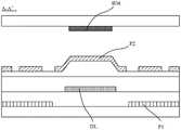
结合图2A~图2D,以及结合表1所示,显示面板100可以为HTR(英文全称:HighTransmittance)显示面板100。该显示面板100具有高透过率,高对比度等效果。Referring to FIG. 2A to FIG. 2D , and referring to Table 1, the
HTR显示面板100中,包括第一电极P1和第二电极P2。其中,第一电极P1可以为公共电极,第二电极P2可以为像素电极。可以将第二电极P2中的锯齿边缘设置在靠近栅线GL的一侧。由此,可以减少数据线DL上方的遮光部BM的宽度,例如缩小至8μm左右。同时在保证充电率的情况下,数据线DL的宽度也缩小,例如缩小至5μm。The
表1、HTR显示面板内各个元件参数Table 1. Parameters of each component in the HTR display panel
如上表1所示,在HTR显示面板100中的扇出区F设有多条扇出线10。扇出线10单层走线设计,位于栅极金属层G(Gate),与栅线GL同层设置。扇出线10的材料一般采用铜(Cu),厚度在
由此可知,各个扇出线10电阻差异较大,会导致显示面板100出现沿第二方向Y延伸的明暗条纹,影响显示面板100的显示效果。It can be seen that the resistance of each fan-out
图3为根据另一些实施例提供的显示面板的结构图。图4为根据又一些实施例提供的显示面板的结构图。图5为根据一些实施例提供的扇出线和数据线连接示意图。Fig. 3 is a structural diagram of a display panel provided according to some other embodiments. Fig. 4 is a structural diagram of a display panel provided according to some other embodiments. Fig. 5 is a schematic diagram of connecting fan-out lines and data lines according to some embodiments.
在一些实施例中,如图3和图4所示,显示面板100包括具有显示区AA和扇出区(英文全称:Fanout)F。In some embodiments, as shown in FIG. 3 and FIG. 4 , the
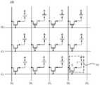
如图3所示,多个像素(sub pixel)P和数据线DL位于显示区AA。多条数据线DL沿第一方向X依次排列,且均沿第二方向Y延伸。为了方便说明,本公开中上述多个像素P是以矩阵形式排列为例进行的说明。此时,沿水平方向X排列成一排的像素P称为一像素行,沿竖直方向Y排列成一排的像素P称为一像素列,一像素行可以与一根栅线GL连接,一像素列可以与一根数据线DL连接。像素P内设置有用于控制像素P进行显示的像素电路,像素电路设置在显示面板100基板上。As shown in FIG. 3 , a plurality of sub pixels P and data lines DL are located in the display area AA. A plurality of data lines DL are arranged in sequence along the first direction X, and all extend along the second direction Y. For the convenience of description, in the present disclosure, the above-mentioned plurality of pixels P are arranged in a matrix form as an example for description. At this time, the pixels P arranged in a row along the horizontal direction X are called a pixel row, and the pixels P arranged in a row along the vertical direction Y are called a pixel column. One pixel row can be connected with one gate line GL, and one pixel Columns can be connected with one data line DL. A pixel circuit for controlling the display of the pixel P is arranged in the pixel P, and the pixel circuit is arranged on the substrate of the
其中,第二方向Y与第一方向X交叉。在一些示例中,如图3所示,第二方向Y与第一方向X垂直。可以理解的是,在另一些示例中,第二方向Y和第一方向X形成的夹角可以为锐角或者钝角。Wherein, the second direction Y intersects the first direction X. In some examples, as shown in FIG. 3 , the second direction Y is perpendicular to the first direction X. It can be understood that, in some other examples, the angle formed by the second direction Y and the first direction X may be an acute angle or an obtuse angle.
以下以显示面板100为液晶显示面板为例,对像素P中的像素电路进行举例说明。The pixel circuit in the pixel P will be described below by taking the
示例性的,如图4所示,像素电路包括晶体管M和液晶电容C。该液晶电容C的两个极板分别由像素电极和公共电极构成。晶体管M的栅极连接栅线GL,第一极连接数据线DL,第二极连接液晶电容C,用于将数据线DL上的数据信号传输至液晶电容C。Exemplarily, as shown in FIG. 4 , the pixel circuit includes a transistor M and a liquid crystal capacitor C. The two plates of the liquid crystal capacitor C are respectively composed of a pixel electrode and a common electrode. The gate of the transistor M is connected to the gate line GL, the first electrode is connected to the data line DL, and the second electrode is connected to the liquid crystal capacitor C for transmitting the data signal on the data line DL to the liquid crystal capacitor C.
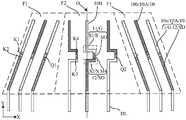
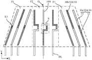
如图5所示,显示面板100还包括多条扇出线10。多条扇出线10位于扇出区F。多条扇出线10沿第一方向X依次排列。As shown in FIG. 5 , the
对于任一条扇出线10,包括彼此连接的第一走线段11和第二走线段12,第一走线段11与第二走线段12异层设置。其中,相邻的两条扇出线10中,一条扇出线10的第一走线段11与一条数据线DL相连,另一条扇出线10的第二走线段12与另一条数据线DL相连。也即,相邻两条扇出线10中,一条扇出线10的第一走线段11与另一条扇出线10的第二走线段12相邻,一条扇出线10的第二走线段12与另一条扇出线10的第一走线段11相邻。For any fan-out
由此,可以实现相邻两条扇出线10中,相对应位置处的走线段异层设置。由此,可以有利于增大了邻两条扇出线10之间的间距,便于扇出线10的走线布局,从而可以通过调节扇出线10的形状,以实现多条扇出线10的长度相等,提高显示面板100的显示效果。同时,增大了相邻两条扇出线10之间的间距,也可以简化刻蚀扇出线10的工艺难度,有利于提高显示面板100刻蚀扇出线10的良率。并且,增大了相邻两条扇出线10之间的间距,也可以便于加宽扇出线10,或者其他走线设计,降低各个扇出线10的电阻,也可以降低各个扇出线10的阻抗,提高显示面板100的显示效果。In this way, it is possible to realize that the wiring segments at corresponding positions in two adjacent fan-out
其中,扇出线10在制作过程中,由于存在一定的不可控的误差(如制作工艺误差、设备精度、测量误差等)。多条扇出线10的长度“相等”可以包括绝对相等和近似相等。也即,扇出线10的长度的浮动范围不超过其自身长度的2%,可以认为多条扇出线10的长度近似相等。Wherein, during the manufacturing process of the fan-out
可以理解的是,多条扇出线10的长度相等时,可以默认多条扇出线10的宽度也是相等的。在一些实施例中,也可以设置多条扇出线10的厚度均相等。在另一些实施例中、多条扇出线10的材料也可以相同。基于此,在使得多条扇出线10的长度相等时,可以使多条扇出线10的电阻相等。由此,可以防止各个扇出线10由于电阻差异较大导致显示面板100出现明暗条纹的问题,可以有利于提高显示面板100的显示效果。It can be understood that when the lengths of the multiple fan-out
此外,对于任意两条扇出线10:一条扇出线10a中的第一走线段11的长度所占的比例,与另一条扇出线10b中的第一走线段11的长度所占的比例相同;一条扇出线10a中的第二走线段12的长度所占的比例,与另一条扇出线10b中的第二走线段12的长度所占的比例相同。In addition, for any two fan-out lines 10: the proportion of the length of the
由于多条扇出线10的长度相等。如此设置,对于任意两条扇出线10:一条扇出线10a中的第一走线段11的长度,与另一条扇出线10b中的第一走线段11的长度相同;一条扇出线10a中的第二走线段12的长度,与另一条扇出线10b中的第二走线段12的长度相同。Since the lengths of the multiple fan-out
可以理解的是,由于第一走线段11和第二走线段12异层设置,也即,第一走线段11和第二走线段12需要两道刻蚀工艺形成,而在不同的刻蚀阶段,存在一定的不可控的误差(如制作工艺误差、设备精度、测量误差等),会导致第一走线段11的宽度和第二走线段12的宽度不等、第一走线段11的厚度和第二走线段12的厚度不等,基于此,均会导致第一走线段11的电阻和第二走线段12的电阻率不同。或者,也存在第一走线段11的材料和第二走线段12的材料不等的情况。基于此,也会导致第一走线段11的电阻和第二走线段12的电阻率不同。It can be understood that since the
例如,对于任意两条扇出线10:一条扇出线10a中,第一走线段11的长度占该扇出线10a的长度的比例为40%、第二走线段12的长度占该扇出线10a的长度的比例为60%,另一条扇出线10b,第一走线段11的长度占该扇出线10b的长度的比例为50%、第二走线段12的长度占该扇出线10b的长度的比例为50%。由于存在一定的不可控的误差,无法直接保证第一走线段11的电阻率和第二走线段12的电阻率相同,基于上述结构,会导致扇出线10a的电阻和扇出线10b的电阻不同,依旧容易导致显示面板100出现明暗条纹,影响显示面板100的显示效果。For example, for any two fan-out lines 10: in one fan-out
而本公开实施例提供的显示面板100,设置一条扇出线10a中的第一走线段11的长度所占的比例,与另一条扇出线10b中的第一走线段11的长度所占的比例相同;一条扇出线10a中的第二走线段12的长度所占的比例,与另一条扇出线10b中的第二走线段12的长度所占的比例相同。可以使各个扇出线10的组成相同,可以防止由于各个扇出线10中,由于第一走线段11和/或第二走线段12对于其扇出线10的占比不同,导致各个扇出线10的电阻不同的问题。从而可以会更有效的降低各个扇出线10的电阻的差异,使各个扇出线10的电阻相等,提高显示面板100的显示效果。In the
示例性的,对于任意两条扇出线10:一条扇出线10a中,第一走线段11的长度占该扇出线10a的长度的比例为40%、第二走线段12的长度占该扇出线10a的长度的比例为60%,另一条扇出线10b,第一走线段11的长度占该扇出线10b的长度的比例为40%、第二走线段12的长度占该扇出线10b的长度的比例为60%。Exemplarily, for any two fan-out lines 10: in one fan-out
示例性的,对于任意两条扇出线10:一条扇出线10a中,第一走线段11的长度占该扇出线10a的长度的比例为45%、第二走线段12的长度占该扇出线10a的长度的比例为55%,另一条扇出线10b,第一走线段11的长度占该扇出线10b的长度的比例为45%、第二走线段12的长度占该扇出线10b的长度的比例为55%。Exemplarily, for any two fan-out lines 10: in one fan-out
对于任意两条扇出线10:一条扇出线10a中,第一走线段11的长度占该扇出线10a的长度的比例为50%、第二走线段12的长度占该扇出线10a的长度的比例为50%,另一条扇出线10b,第一走线段11的长度占该扇出线10b的长度的比例为50%、第二走线段12的长度占该扇出线10b的长度的比例为50%。For any two fan-out lines 10: in one fan-out
综上所述,本公开实施例提供的显示面板100,在设置各个扇出线10的长度均相等的基础上,限定扇出线10包括异层设置的第一走线段11和第二走线段12,相邻两条扇出线10中,一条扇出线10的第一走线段11与另一条扇出线10的第二走线段12相邻,一条扇出线10的第二走线段12与另一条扇出线10的第一走线段11相邻。且对于任意两条扇出线10:一条扇出线10a中的第一走线段11的长度所占的比例,与另一条扇出线10b中的第一走线段11的长度所占的比例相同;一条扇出线10a中的第二走线段12的长度所占的比例,与另一条扇出线10b中的第二走线段12的长度所占的比例相同。可以在便于扇出线10走线布局的情况下,更好调节各个扇出线10的长度,使各个扇出线10的长度可以相等,以及设置相同占比的走线段,可以更进一步的降低各个扇出线10的电阻的差异,使各个扇出线10的电阻相等,防止显示面板出现明暗条纹的问题,从而提高显示面板100的显示效果。To sum up, in the
其中,上述所述“长度”均可以理解为沿扇出线的延伸方向上的长度。例如,当走线具有弯折的情况下,其“长度”指的是包括其弯折方向上的长度。下文对于“长度”的解释同样适用。Wherein, the above-mentioned "length" can be understood as the length along the extending direction of the fan-out line. For example, when the trace has a bend, its "length" refers to the length in the direction of the bend. The explanation below for "length" also applies.
在一些实施例中,如图5所示,显示面板100包括栅极导电层和源漏导电层。源漏导电层位于栅极导电层靠近显示面板100的出光面的一侧。也即,源漏导电层位于栅极导电层的上方。In some embodiments, as shown in FIG. 5 , the
在一些示例中,数据线DL位于源漏导电层SD、栅线GL位于栅极导电层G。基于此,对于任一条扇出线10,包括彼此连接的第一走线段11和第二走线段12,第一走线段11与第二走线段12异层设置的情况下:可以设置第一走线段11与栅线GL同层,位于栅极导电层G;第二走线段12与数据线DL同层,位于源漏导电层SD。In some examples, the data line DL is located in the source-drain conductive layer SD, and the gate line GL is located in the gate conductive layer G. Based on this, for any fan-out
如此设置,第一走线段11与栅线GL可以用同一道制图工艺形成,第二走线段12与数据线DL可以用同一道制图工艺形成。由此,可以简化显示面板100的制程。此外,当扇出线10的第二走线段12与数据线DL电连接时,可以直接一体化形成,无需设置打孔工艺等,简化工艺难度。而当扇出线10的第一走线段11与数据线DL电连接时,第一走线段11与数据线DL可以通过过孔实现电连接。本公开实施例对第一走线段11与数据线DL的连接防止不做限定,也可以通过导电结构等跨桥方式连接。In this way, the
示例性的,栅极导电层G的材料包括导电金属。该导电金属可以包括铝、铜、钼中的至少一种,本公开不限于此。Exemplarily, the material of the gate conductive layer G includes conductive metal. The conductive metal may include at least one of aluminum, copper, and molybdenum, to which the present disclosure is not limited.
示例性的,源漏导电层SD的材料包括导电金属。该导电金属可以包括铜,但本公开不限于此。Exemplarily, the material of the source-drain conductive layer SD includes conductive metal. The conductive metal may include copper, but the present disclosure is not limited thereto.
示例性的,栅极导电层G和源漏导电层SD之间设置有绝缘层,绝缘层使栅极导电层和源漏导电层之间电绝缘。例如,绝缘层的材料包括氮化硅、氮氧化硅和氧化硅的无机绝缘材料中的任一种。绝缘层的材料可以包括二氧化硅,本公开不限于此。Exemplarily, an insulating layer is disposed between the gate conductive layer G and the source-drain conductive layer SD, and the insulating layer electrically insulates the gate conductive layer from the source-drain conductive layer. For example, the material of the insulating layer includes any one of inorganic insulating materials of silicon nitride, silicon oxynitride, and silicon oxide. The material of the insulating layer may include silicon dioxide, to which the present disclosure is not limited.
在一些实施例中,如图5所示,显示面板100内相邻的两条扇出线10中,一条扇出线10a的第一走线段11的长度与另一条扇出线10b的第二走线段12的长度相等。In some embodiments, as shown in FIG. 5, among the two adjacent fan-out
由于各个扇出线10的长度均相等,且对于任意两条扇出线10:一条扇出线10a中的第一走线段11的长度所占的比例,与另一条扇出线10b中的第一走线段11的长度所占的比例相同;一条扇出线10a中的第二走线段12的长度所占的比例,与另一条扇出线10b中的第二走线段12的长度所占的比例相同。Since the lengths of each fan-out
在此基础上,设置相邻的两条扇出线10中,一条扇出线10a的第一走线段11的长度与另一条扇出线10b的第二走线段12的长度相等。也即,相邻的两条扇出线10中,扇出线10a的第一走线段11的长度、扇出线10a的第二走线段12的长度、扇出线10b的第一走线段11的长度,以及扇出线10b的第二走线段12的长度均相等。On this basis, among the two adjacent fan-out
也即可以理解为,对于任意两条扇出线10:一条扇出线10a中,第一走线段11的长度占该扇出线10a的长度的比例为50%、第二走线段12的长度占该扇出线10a的长度的比例为50%,另一条扇出线10b,第一走线段11的长度占该扇出线10b的长度的比例为50%、第二走线段12的长度占该扇出线10b的长度的比例为50%。That is to say, for any two fan-out lines 10: in one fan-out
如此设置,一方面,任一条扇出线10中的第一走线段11和第二走线段12各占一半,使得第一走线段11的长度和第二走线段12长度均衡,便于形成第一走线段11和第二走线段12,简化扇出线10的制程难度。另一方面,也可以更好的实现相邻两条扇出线10中,一条扇出线10的第一走线段11,与另一条扇出线10的第二走线段12相邻,与另一条扇出线10的第一走线段11不相邻。一条扇出线10的第二走线段12,与另一条扇出线10的第一走线段11相邻,与另一条扇出线10的第二走线段12不相邻。In this way, on the one hand, the
由此,可以更好的实现相邻两条扇出线10中,相对应位置处的走线段异层设置。由此,可以有利于增大了邻两条扇出线10之间的间距,防止相邻两条扇出线10中第一走线段11之间相接触发生短路,和/或,防止相邻两条扇出线10中第二走线段12之间相接触发生短路。便于扇出线10的走线布局,提高显示面板100刻蚀扇出线10的良率。As a result, it is possible to better implement different-layer arrangement of the routing segments at corresponding positions in two adjacent fan-out
其中,图5以在垂直第一走线段11所在平面的方向上(在沿显示面板100厚度的方向上),第一走线段11和第二走线段12未交叠为例。可以理解的是,在另一些实施例中,可以设置相邻的两条扇出线10中第一走线段11和第二走线段12至少部分交叠。但是,此时需设置相邻两条扇出线10连接端部位置处不交叠,也即相邻两条扇出线10连接端部位置处可交错设置,避免实现第一走线段11和第二走线段12电连接时,发生短路的问题。In FIG. 5 , in the direction perpendicular to the plane where the
在一些实施例中,扇出线10的线宽在3.5μm~5μm。例如,第一走线段11的线宽在3.5μm~5μm。和/或,第二走线段12的线宽在3.5μm~5μm。In some embodiments, the line width of the fan-out
当扇出线10的线宽在等于或趋近于3.5μm时,扇出线10的线宽较窄,可以在防止扇出线10电阻过大的同时更好的节省扇出区F的空间,更便于走线布局。当扇出线10的线宽在等于或趋近于5μm时,扇出线10的线宽较宽,可以更好的降低扇出线10的电阻的同时防止扇出线10线宽过宽影响走线布局。When the line width of the fan-out
在一些示例中,第一走线段11的线宽等于第二走线段12的线宽。可以更好的通过调节第一走线段11的长度和第二走线段12的长度,改变扇出线10的电阻。以此,降低各个扇出线10的电阻的差异,使各个扇出线10的电阻相等,防止显示面板出现明暗条纹的问题,从而提高显示面板100的显示效果。In some examples, the line width of the
在一些实施例中,如图3所示,显示面板100可以采用覆晶薄膜(Chip On Film,COF)技术。COF技术是一种将驱动芯片IC固定于柔性电路板(Flexible Printed Circuit,FPC)上晶粒软膜构装技术,运用软质附加电路板作封装芯片载体将芯片与软性基板电路接合的技术。常规的显示面板中,驱动芯片IC设置在显示面板100的下边框,而采用COF技术,将显示面板上的驱动芯片IC集成到FPC上组成COF柔性电路板,COF柔性电路板和绑定区BB电连接。将COF柔性电路板折到显示面板的背后,节省了下边框的空间,可实现下边框的窄化。In some embodiments, as shown in FIG. 3 , the
在一些实施例中,如图5所示,显示面板100中的扇出区F包括:沿第一方向X排布的两个边缘区域F1,以及位于两个边缘区域F1之间的中间区域F2。多条扇出线10中,位于边缘区域F1的扇出线10定义为第一扇出线10A。第一扇出线10A自靠近显示区AA的一端至远离显示区AA的一端,逐渐靠近显示面板100的中轴线O,中轴线O平行于第二方向Y。In some embodiments, as shown in FIG. 5 , the fan-out area F in the
设置位于边缘区域F1的第一扇出线10A自靠近显示区AA的一端至远离显示区AA的一端,逐渐靠近显示面板100的中轴线O。可以使扇出区F呈现扇形,远离显示区AA一侧收紧,便于减小后续绑定宽度。The first fan-out
多条扇出线10中,位于边缘区域F1的扇出线10定义为第二扇出线10B。第二扇出线10B中包括蛇形走线S。Among the plurality of fan-out
由于位于边缘区域F1的第一扇出线10A自靠近显示区AA的一端至远离显示区AA的一端,逐渐靠近显示面板100的中轴线O。会导致位于边缘区域F1内的第一扇出线10A的长度较长。设置第二扇出线10B中包括蛇形走线S,以使第二扇出线10B的长度与第一扇出线10A的长度相等。也即使得各个扇出线10的长度均相等。基于此,可以使多条扇出线10的电阻近似相等。由此,可以防止各个扇出线10由于电阻差异较大导致显示面板100出现明暗条纹的问题,可以有利于提高显示面板100的显示效果。Since the first fan-out
其中,相等包括绝对相等和近似相等。也即,第二扇出线10B的长度与第一扇出线10A的长度的差值的浮动范围不超过各自长度的2%,可以认为第二扇出线10B的长度与第一扇出线10A的长度近似相等,也即各个扇出线10的长度均相等。Wherein, equality includes absolute equality and approximate equality. That is, the floating range of the difference between the length of the second fan-out
在一些实施例中,多条扇出线10之间的电阻差小于或等于600Ω。具体图下:In some embodiments, the resistance difference between the plurality of fan-out
第一种:多条第一扇出线10A之间的电阻差小于或等于600Ω。The first type: the resistance difference between the multiple first fan-out
示例性的,在对于任意两条第一扇出线10A:一条扇出线10a中,第一走线段11的长度占该扇出线10a的长度的比例为50%、第二走线段12的长度占该扇出线10a的长度的比例为50%,另一条扇出线10b,第一走线段11的长度占该扇出线10b的长度的比例为50%、第二走线段12的长度占该扇出线10b的长度的比例为50%的情况下,限定各个走线段(第一走线段11和第二走线段12)的偏差值在扇出线10长度的±1%上下浮动。Exemplarily, for any two first fan-out
也即,限定一条扇出线10a中,第一走线段11的长度占该扇出线10a的长度的比例为50%、或者50%±1%;第二走线段12的长度占该扇出线10a的长度的比例为50%,或者50%±1%;另一条扇出线10b,第一走线段11的长度占该扇出线10b的长度的比例为50%,或者50%±1%;第二走线段12的长度占该扇出线10b的长度的比例为50%,或者50%±1%。That is, in defining a fan-out
基于此,结合下表2所示,当各个走线段(第一走线段11和第二走线段12)的偏差值在扇出线10长度的±1%上下浮动时,可以使多条第一扇出线10A之间的电阻差小于或等于10Ω。Based on this, as shown in Table 2 below, when the deviation value of each routing segment (the
以扇出线10a为例:表2中:Take the fan-out
第一走线段+0%表示,第一走线段11的长度占该扇出线10a的长度的比例为50%时,无发生误差。也即,此时第一走线段11的长度占该扇出线10a的长度的比例为50%。The first routing segment+0% means that when the length of the
第一走线段-1%表示,第一走线段11的长度占该扇出线10a的长度的比例为50%时,发生-1%的误差。也即,此时第一走线段11的长度占该扇出线10a的长度的比例为49%。The first routing segment -1% means that when the length of the
第一走线段+1%表示,第一走线段11的长度占该扇出线10a的长度的比例为50%时,发生+1%的误差。也即,此时第一走线段11的长度占该扇出线10a的长度的比例为51%。+1% of the first routing segment means that when the length of the
表2第一走线长度占比、第二走线长度占比与电阻、灰阶的关系表Table 2 The relationship between the proportion of the length of the first trace, the proportion of the length of the second trace, resistance, and gray scale

在一些示例中,结合上表2所示,在扇出线10a和扇出线10b内,当第一走线段11和第二走线段12偏差值浮动范围相同时。也即,在保证对于任意两条扇出线10:一条扇出线10a中的第一走线段11的长度所占的比例,与另一条扇出线10b中的第一走线段11的长度所占的比例相同;一条扇出线10a中的第二走线段12的长度所占的比例,与另一条扇出线10b中的第二走线段12的长度所占的比例相同时,扇出线10a和扇出线10b最大差值为2.6Ω,该电阻差值已经在极小的范围内,可以使得流经第一扇出线10A至数据线DL的信号差值较小。从而,使得与多条数据线DL对应连接的各个像素列之间的灰阶差异较小,降低显示面板100内各个像素列之间的亮度差异。In some examples, as shown in Table 2 above, in the fan-out
在一些示例中,各个像素列的之间亮度的差值小于3个灰阶。In some examples, the brightness difference between the respective pixel columns is less than 3 gray scales.
示例性的,结合上表2所示,例如,各个像素列之间的亮度差值小于1个灰阶。本公开对此不做限定,在误差浮动范围较小时,各个像素列之间的亮度差值小于0.08、0.06、0.04或0.03中任一值个灰阶。Exemplarily, as shown in Table 2 above, for example, the luminance difference between each pixel column is less than 1 gray scale. The present disclosure does not limit this, and when the error floating range is small, the brightness difference between each pixel column is less than any one of 0.08, 0.06, 0.04 or 0.03 gray levels.
由此可知,在对于任意两条扇出线10:一条扇出线10a中的第一走线段11的长度所占的比例,与另一条扇出线10b中的第一走线段11的长度所占的比例相同;一条扇出线10a中的第二走线段12的长度所占的比例,与另一条扇出线10b中的第二走线段12的长度所占的比例相同时;在扇出线10误差在±1范围内浮动时,各个像素列的亮度差值小于1灰阶,可以显著降低显示面板100内各个像素列之间的亮度差异,防止显示面板100出现明暗条纹的问题,可以有利于提高显示面板100的显示效果。It can be seen from this that, for any two fan-out lines 10: the ratio of the length of the
第二种:多条第二扇出线10B之间的电阻差小于或等于600Ω。The second type: the resistance difference between the plurality of second fan-out
示例性的,在对于任意两条第二扇出线10B:一条扇出线10a中,第一走线段11的长度占该扇出线10a的长度的比例为50%、第二走线段12的长度占该扇出线10a的长度的比例为50%,另一条扇出线10b,第一走线段11的长度占该扇出线10b的长度的比例为50%、第二走线段12的长度占该扇出线10b的长度的比例为50%的情况下,限定各个走线段(第一走线段11和第二走线段12)的偏差值在扇出线10长度的±1%上下浮动。Exemplarily, for any two second fan-out
也即,限定一条扇出线10a中,第一走线段11的长度占该扇出线10a的长度的比例为50%、或者50%±1%;第二走线段12的长度占该扇出线10a的长度的比例为50%,或者50%±1%;另一条扇出线10b,第一走线段11的长度占该扇出线10b的长度的比例为50%,或者50%±1%;第二走线段12的长度占该扇出线10b的长度的比例为50%,或者50%±1%。That is, in defining a fan-out
基于此,结合下表3所示,当各个走线段(第一走线段11和第二走线段12)的偏差值在扇出线10长度的±1%上下浮动时,可以使多条第二扇出线10B之间的电阻差小于或等于10Ω。Based on this, as shown in Table 3 below, when the deviation value of each routing segment (the
以扇出线10a为例。表3中:Take the fan-out
第一走线段+0%表示,第一走线段11的长度占该扇出线10a的长度的比例为50%时,无发生误差。也即,此时第一走线段11的长度占该扇出线10a的长度的比例为50%。The first routing segment+0% means that when the length of the
第一走线段-1%表示,第一走线段11的长度占该扇出线10a的长度的比例为50%时,发生-1%的误差。也即,此时第一走线段11的长度占该扇出线10a的长度的比例为49%。The first routing segment -1% means that when the length of the
第一走线段+1%表示,第一走线段11的长度占该扇出线10a的长度的比例为50%时,发生+1%的误差。也即,此时第一走线段11的长度占该扇出线10a的长度的比例为51%。+1% of the first routing segment means that when the length of the
表3第一走线长度占比、第二走线长度占比与电阻、灰阶的关系表Table 3 The relationship between the proportion of the length of the first trace, the proportion of the length of the second trace, resistance, and gray scale

在一些示例中,结合上表3所示,在扇出线10a和扇出线10b内,当第一走线段11和第二走线段12偏差值浮动范围相同时,也即,在保证对于任意两条扇出线10:一条扇出线10a中的第一走线段11的长度所占的比例,与另一条扇出线10b中的第一走线段11的长度所占的比例相同;一条扇出线10a中的第二走线段12的长度所占的比例,与另一条扇出线10b中的第二走线段12的长度所占的比例相同时,相邻的扇出线10a和扇出线10b最大差值为2.6Ω,该电阻差值已经在极小的范围内,可以使得流经第一扇出线10A至数据线DL的信号差值较小。从而,使得与多条数据线DL对应连接的各个像素列之间的灰阶差异较小,降低显示面板100内各个像素列之间的亮度差异。In some examples, as shown in Table 3 above, in the fan-out
在一些示例中,各个像素列的之间亮度的差值小于3个灰阶。In some examples, the brightness difference between the respective pixel columns is less than 3 gray scales.
示例性的,结合上表2所示,例如,各个像素列之间的亮度差值小于1个灰阶。本公开对此不做限定,在误差浮动范围较小时,各个像素列之间的亮度差值小于0.08、0.06、0.04或0.03中任一值个灰阶。Exemplarily, as shown in Table 2 above, for example, the luminance difference between each pixel column is less than 1 gray scale. The present disclosure does not limit this, and when the error floating range is small, the brightness difference between each pixel column is less than any one of 0.08, 0.06, 0.04 or 0.03 gray levels.
由此可知,在保证对于任意两条扇出线10:一条扇出线10a中的第一走线段11的长度所占的比例,与另一条扇出线10b中的第一走线段11的长度所占的比例相同;一条扇出线10a中的第二走线段12的长度所占的比例,与另一条扇出线10b中的第二走线段12的长度所占的比例相同时,在扇出线10误差在±1范围内浮动时,各个像素列的亮度差值小于1灰阶,可以显著降低显示面板100内各个像素列之间的亮度差异,防止显示面板100出现明暗条纹的问题,可以有利于提高显示面板100的显示效果。It can be seen that, for any two fan-out lines 10: the ratio of the length of the
在一些实施例中,结合表2和表3所示,无论是对于第一扇出线10A还是对于第二扇出线10B,通过上述方式均可以使得各个扇出线10之间的电阻差值较低,可以显著降低显示面板100内各个像素列之间的亮度差异,防止显示面板100出现明暗条纹的问题,可以有利于提高显示面板100的显示效果。In some embodiments, as shown in Table 2 and Table 3, whether it is for the first fan-out
在一些实施例中,结合表2和表3所示,在对于任意两条扇出线10:一条扇出线10a中的第一走线段11的长度所占的比例,与另一条扇出线10b中的第一走线段11的长度所占的比例相同;一条扇出线10a中的第二走线段12的长度所占的比例,与另一条扇出线10b中的第二走线段12的长度所占的比例相同时:当各个走线段(第一走线段11和第二走线段12)的偏差值在扇出线10长度的±1%上下浮动时,可以使多条扇出线10之间的电阻差小于或等于600Ω。该电阻差值已经在很小的范围内,可以使得流经扇出线10至数据线DL的信号差值较小。从而,使得与多条数据线DL对应连接的各个像素列之间的灰阶差异较小,降低显示面板100内各个像素列之间的亮度差异。In some embodiments, as shown in Table 2 and Table 3, for any two fan-out lines 10: the ratio of the length of the
示例性的,使得与多条数据线DL对应连接的各个像素列之间的灰阶差小于3。例如,与多条数据线DL对应连接的各个像素列之间的灰阶差小于1、0.08、0.06、0.04或0.03中任一值。Exemplarily, the gray scale difference between the respective pixel columns correspondingly connected to the multiple data lines DL is less than 3. For example, the gray scale difference between the pixel columns correspondingly connected to the plurality of data lines DL is smaller than any one of 1, 0.08, 0.06, 0.04 or 0.03.
示例性的,第一扇出线10A总电阻和第二扇出线10B总电阻的最大差值约在400Ω左右(2480Ω-2024Ω)。相对于一些实现方式中电阻差值在2300Ω左右,在400Ω电阻差值范围内可利用绑定区BB内的补偿结构将其补偿,从而降低显示面板100内各个像素列之间的亮度差异,防止显示面板100出现明暗条纹的问题,可以有利于提高显示面板100的显示效果。Exemplarily, the maximum difference between the total resistance of the first fan-out
例如,可以使多条扇出线10之间的电阻差小于或等于500Ω、400Ω、300Ω、200Ω、100Ω、50Ω或30Ω中任一个。For example, the resistance difference among the plurality of fan-out
在一些实施例中,如图5所示,显示面板100在第一扇出线10A中,第一走线段11包括第一直线段L1和第一连接端部M1,第二走线段12包括第二直线段L2和第二连接端部M2。显示面板100还包括第一导电连接层Q1,第一导电连接层Q1通过第一过孔K1电连接至第一连接端部M1,且第一导电连接层Q1通过第二过孔K2电连接至第二连接端部M2。In some embodiments, as shown in FIG. 5 , the
第一导电连接层Q1与第一走线段11异层设置,通过第一过孔K1电连接至第一连接端部M1。并且,第一导电连接层Q1与第二走线段12异层设置。第一导电连接层Q1通过第二过孔K2电连接至第二连接端部M2。由此实现第一走线段11和第二走线段12电连接。The first conductive connection layer Q1 is arranged in a different layer from the
在一些示例中,显示面板100还包括透明电极层I,透明电极层I位于源漏导电层SD远离栅极导电层G的一侧。第一导电连接层Q1可以位于透明电极层I。透明电极层还可以包括像素电极或公共电极。In some examples, the
示例性的,透明电极层I的材料可以为氧化铟锡(Indium Tin Oxide,简称ITO),但本公开对此不做限定。Exemplarily, the material of the transparent electrode layer I may be indium tin oxide (Indium Tin Oxide, ITO for short), but this disclosure is not limited thereto.
在一些示例中,第一导电连接层Q1通过至少一个第一过孔K1电连接至第一连接端部M1。In some examples, the first conductive connection layer Q1 is electrically connected to the first connection terminal M1 through at least one first via hole K1 .
示例性的,第一导电连接层Q1通过一个第一过孔K1电连接至第一连接端部M1。Exemplarily, the first conductive connection layer Q1 is electrically connected to the first connection terminal M1 through a first via hole K1 .
当第一导电连接层Q1通过一个第一过孔K1电连接至第一连接端部M1时,可以设置第一过孔K1的尺寸与第一导电连接层Q1的宽度大致相等,只要使得沿垂直第一导电连接层Q1所在平面的方向上,第一导电连接层Q1覆盖第一过孔K1即可,保证可以实现第一导电连接层Q1和第一连接端部M1电连接。此外,设置第一过孔K1的尺寸与第一导电连接层Q1的宽度大致相等,可以增加第一导电连接层Q1和第一连接端部M1的接触面积,降低第一导电连接层Q1和第一连接端部M1的接触电阻,防止第一导电连接层Q1和第一连接端部M1出现搭接不良的问题。When the first conductive connection layer Q1 is electrically connected to the first connection terminal M1 through a first via hole K1, the size of the first via hole K1 can be set to be approximately equal to the width of the first conductive connection layer Q1, as long as the vertical In the direction of the plane where the first conductive connection layer Q1 is located, it is enough that the first conductive connection layer Q1 covers the first via hole K1 to ensure that the first conductive connection layer Q1 and the first connection end M1 can be electrically connected. In addition, setting the size of the first via hole K1 to be approximately equal to the width of the first conductive connection layer Q1 can increase the contact area between the first conductive connection layer Q1 and the first connection end M1, and reduce the contact area between the first conductive connection layer Q1 and the second connection layer Q1. The contact resistance of the first connection end M1 prevents the problem of poor overlap between the first conductive connection layer Q1 and the first connection end M1.
示例性的,第一导电连接层Q1通过多个第一过孔K1电连接至第一连接端部M1。Exemplarily, the first conductive connection layer Q1 is electrically connected to the first connection terminal M1 through a plurality of first via holes K1 .
当第一导电连接层Q1通过多个第一过孔K1电连接至第一连接端部M1时,可以设置多个第一过孔K1沿第一直线段L1的延伸方向排布,也可以设置多个第一过孔K1沿垂直第一直线段L1的延伸方向排布,或者,多个第一过孔K1阵列排布。只要使得沿垂直第一导电连接层Q1所在平面的方向上,第一导电连接层Q1覆盖全部第一过孔K1即可,保证可以实现第一导电连接层Q1和第一连接端部M1电连接。此外,设置第一导电连接层Q1通过多个第一过孔K1电连接至第一连接端部M1时,第一过孔K1的直径较小一些,可以有利于降低第一过孔K1的刻蚀工艺难度,提高第一导电连接层Q1和第一连接端部M1的搭接良率。When the first conductive connection layer Q1 is electrically connected to the first connection end M1 through a plurality of first via holes K1, a plurality of first via holes K1 may be arranged along the extending direction of the first straight line segment L1, or a plurality of first via holes K1 may be arranged. The plurality of first via holes K1 are arranged along the extending direction perpendicular to the first straight line segment L1, or the plurality of first via holes K1 are arranged in an array. As long as the first conductive connection layer Q1 covers all the first via holes K1 along the direction perpendicular to the plane where the first conductive connection layer Q1 is located, it is enough to ensure that the first conductive connection layer Q1 and the first connection terminal M1 can be electrically connected. . In addition, when the first conductive connection layer Q1 is set to be electrically connected to the first connection end M1 through a plurality of first via holes K1, the diameter of the first via holes K1 is smaller, which can help reduce the marking of the first via holes K1. The difficulty of the etching process is improved, and the overlapping yield of the first conductive connection layer Q1 and the first connection end M1 is improved.
综上,本公开实施例对第一过孔K1的数量不做具体限定,可以根据实际情况设置。此外,本公开实施例对第一过孔K1的形状也不做限定,可以为圆形或方形等形状。To sum up, the embodiment of the present disclosure does not specifically limit the number of the first via holes K1, which may be set according to actual conditions. In addition, the embodiments of the present disclosure do not limit the shape of the first via hole K1 , which may be circular or square.
在一些示例中,第一导电连接层Q1通过一个第二过孔K2电连接至第二连接端部M2。In some examples, the first conductive connection layer Q1 is electrically connected to the second connection terminal M2 through a second via hole K2.
示例性的,第一导电连接层Q1通过一个第二过孔K2电连接至第二连接端部M2。Exemplarily, the first conductive connection layer Q1 is electrically connected to the second connection terminal M2 through a second via hole K2.
当第一导电连接层Q1通过一个第二过孔K2电连接至第二连接端部M2时,可以设置第二过孔K2的尺寸与第一导电连接层Q1的宽度大致相等,只要使得沿垂直第一导电连接层Q1所在平面的方向上,第一导电连接层Q1覆盖第二过孔K2即可,保证可以实现第一导电连接层Q1和第二连接端部M2电连接。此外,设置第二过孔K2的尺寸与第一导电连接层Q1的宽度大致相等,可以增加第一导电连接层Q1和第二连接端部M2的接触面积,降低第一导电连接层Q1和第二连接端部M2的接触电阻,防止第一导电连接层Q1和第二连接端部M2出现断路等搭接不良的问题。When the first conductive connection layer Q1 is electrically connected to the second connection terminal M2 through a second via hole K2, the size of the second via hole K2 can be set to be approximately equal to the width of the first conductive connection layer Q1, as long as the vertical In the direction of the plane where the first conductive connection layer Q1 is located, it is enough that the first conductive connection layer Q1 covers the second via hole K2 to ensure that the first conductive connection layer Q1 and the second connection end M2 can be electrically connected. In addition, setting the size of the second via hole K2 to be approximately equal to the width of the first conductive connection layer Q1 can increase the contact area between the first conductive connection layer Q1 and the second connection end M2, and reduce the contact area between the first conductive connection layer Q1 and the second connection end M2. The contact resistance of the two connection ends M2 prevents problems such as disconnection of the first conductive connection layer Q1 and the second connection end M2 due to poor overlap.
示例性的,第一导电连接层Q1通过多个第二过孔K2电连接至第二连接端部M2。Exemplarily, the first conductive connection layer Q1 is electrically connected to the second connection terminal M2 through a plurality of second via holes K2.
当第一导电连接层Q1通过多个第二过孔K2电连接至第二连接端部M2时,可以设置多个第二过孔K2沿第二直线段L2的延伸方向排布,也可以设置多个第二过孔K2沿垂直第二直线段L2的延伸方向排布,或者,多个第二过孔K2阵列排布。只要使得沿垂直第一导电连接层Q1所在平面的方向上,第一导电连接层Q1覆盖全部第二过孔K2即可,保证可以实现第一导电连接层Q1和第二连接端部M2电连接。此外,设置第一导电连接层Q1通过多个第二过孔K2电连接至第二连接端部M2时,第二过孔K2的直径较小一些,可以有利于降低第二过孔K2的刻蚀工艺难度,提高第一导电连接层Q1和第二连接端部M2的搭接良率。When the first conductive connection layer Q1 is electrically connected to the second connection end M2 through a plurality of second via holes K2, a plurality of second via holes K2 may be arranged along the extending direction of the second straight line segment L2, or a plurality of second via holes K2 may be arranged. The multiple second via holes K2 are arranged along the extending direction perpendicular to the second straight line segment L2, or the multiple second via holes K2 are arranged in an array. As long as the first conductive connection layer Q1 covers all the second via holes K2 along the direction perpendicular to the plane where the first conductive connection layer Q1 is located, it is ensured that the electrical connection between the first conductive connection layer Q1 and the second connection end M2 can be realized. . In addition, when the first conductive connection layer Q1 is set to be electrically connected to the second connection end M2 through a plurality of second via holes K2, the diameter of the second via holes K2 is smaller, which is beneficial to reduce the marking of the second via holes K2. The difficulty of the etching process is improved, and the overlapping yield of the first conductive connection layer Q1 and the second connection end M2 is improved.
在一些实施例中,如图5所示,显示面板100中在第一扇出线10A中,第一走线段11包括第一直线段L1和第一连接端部M1,第二走线段12包括第二直线段L2和第二连接端部M2。显示面板100还包括第一导电连接层Q1,第一导电连接层Q1通过第一过孔K1电连接至第一连接端部M1,且第一导电连接层Q1通过第二过孔K2电连接至第二连接端部M2。In some embodiments, as shown in FIG. 5 , in the first fan-out
基于此,设置第一连接端部M1的线宽等于第一直线段L1的线宽;和/或,第二连接端部M2的线宽等于第二直线段L2的线宽。Based on this, the line width of the first connecting end M1 is set equal to the line width of the first straight line segment L1; and/or, the line width of the second connecting end M2 is equal to the line width of the second straight line segment L2.
上述结构可以包括以下几种情况:The above structure can include the following situations:
第一种:如图5所示的第一走线段11。第一连接端部M1的线宽等于第一直线段L1的线宽。相当于第一走线段11在任意位置处的宽度均相等。一方面,可以降低工艺难度,简化工艺制程。另一方面,可以节省扇出区F的空间,有利于扇出线10的走线布局。The first type: the
第二种:如图5所示的第二走线段12。第二连接端部M2的线宽等于第二直线段L2的线宽。相当于第二走线段12在任意位置处的宽度均相等。一方面,可以降低工艺难度,简化工艺制程。另一方面,可以节省扇出区F的空间,有利于扇出线10的走线布局。The second type: the
第三种:如图5所示的第一走线段11和第二走线段12。第一连接端部M1的线宽等于第一直线段L1的线宽,且第二连接端部M2的线宽等于第二直线段L2的线宽。相当于第一走线段11在任意位置处的宽度均相等,且第二走线段12在任意位置处的宽度均相等。一方面,可以降低工艺难度,简化工艺制程。另一方面,可以节省扇出区F的空间,有利于扇出线10的走线布局。The third type: the
图6为根据一些实施例提供的扇出区的结构图。FIG. 6 is a structural diagram of a fan-out zone provided according to some embodiments.
在一些实施例中,如图6所示,显示面板100中在第一扇出线10A中,第一走线段11包括第一直线段L1和第一连接端部M1,第二走线段12包括第二直线段L2和第二连接端部M2。显示面板100还包括第一导电连接层Q1,第一导电连接层Q1通过第一过孔K1电连接至第一连接端部M1,且第一导电连接层Q1通过第二过孔K2电连接至第二连接端部M2。In some embodiments, as shown in FIG. 6 , in the first fan-out
基于此,设置第一连接端部M1的线宽大于第一直线段L1的线宽;和/或,第二连接端部M2的线宽大于第二直线段L2的线宽。Based on this, the line width of the first connection end portion M1 is set to be greater than the line width of the first straight line segment L1; and/or, the line width of the second connection end portion M2 is greater than the line width of the second line segment L2.
上述结构可以包括以下几种情况:The above structure can include the following situations:
第一种:如图6所示的第一走线段11。第一连接端部M1的线宽DM1大于第一直线段L1的线宽DL1。The first type: the
第一走线段11通过第一连接端部M1与第二走线段12电连接,设置第一连接端部M1的线宽DM1大于第一直线段L1的线宽DL1,可以增加第一走线段11与第二走线段12电连接位置处的面积。一方面,增大第一走线段11第一连接端部M1的面积,便于设置第一过孔K1,实现第一导电连接层Q1通过第一过孔K1电连接至第一连接端部M1。另一方面,增大第一走线段11第一连接端部M1的面积,可以降低第一导电连接层Q1和第一连接端部M1的接触电阻,防止第一导电连接层Q1和第一连接端部M1出现搭接不良的问题。The
其中,本公开实施例对第一连接端部M1的线宽DM1大于第一直线段L1的线宽DL1的范围不做限定,可以根据扇出区F的空间进行调节设置。Wherein, the embodiment of the present disclosure does not limit the range in which the line width DM1 of the first connection end M1 is greater than the line width DL1 of the first straight line segment L1 , which can be adjusted and set according to the space of the fan-out area F.
第二种:如图6所示的第二走线段12。第二连接端部M2的线宽DM2大于第二直线段L2的线宽DL2。The second type: the
第二走线段12通过第二连接端部M2与第一走线段11电连接,设置第二连接端部M2的线宽DM2大于第二直线段L2的线宽DL2,可以增加第二走线段12与第一走线段11电连接位置处的面积。一方面,增大第二走线段12第二连接端部M2的面积,便于设置第二过孔K2,实现第一导电连接层Q1通过第二过孔K2电连接至第二连接端部M2。另一方面,增大第二走线段12第二连接端部M2的面积,可以降低第一导电连接层Q1和第二连接端部M2的接触电阻,防止第一导电连接层Q1和第二连接端部M2出现搭接不良的问题。The
其中,本公开实施例对第二连接端部M2的线宽大于第二直线段L2的线宽的范围不做限定,可以根据扇出区F的空间进行调节设置。Wherein, the embodiment of the present disclosure does not limit the range in which the line width of the second connection end portion M2 is greater than the line width of the second straight line segment L2, which can be adjusted and set according to the space of the fan-out area F.
第三种:如图6所示的第一走线段11和第二走线段12。第一连接端部M1的线宽DM1大于第一直线段L1的线宽DL1,且第二连接端部M2的线宽DM2大于第二直线段L2的线宽DL2。The third type: the
第一走线段11通过第一连接端部M1与第二走线段12通过第二连接端部M2电连接,设置第一连接端部M1的线宽DM1大于第一直线段L1的线宽DL1,且第二连接端部M2的线宽DM2大于第二直线段L2的线宽DL2。可以增大第一走线段11和第二走线段12电连接位置处的面积。既可以便于设置第一过孔K1和第二过孔K2,有利于实现第一走线段11和第二走线段12电连接。还可以降低第一走线段11和第二走线段12的接触电阻,防止第一连接端部M1和第二连接端部M2出现搭接不良的问题。The
其中,本公开实施例对第一连接端部M1的线宽DM1大于第一直线段L1的线宽DL1的范围不做限定;以及,对第二连接端部M2的线宽DM2大于第二直线段L2的线宽DL2的范围不做限定,可以根据扇出区F的空间进行调节设置。Wherein, the embodiment of the present disclosure does not limit the range in which the line width DM1 of the first connection end M1 is greater than the line width DL1 of the first straight line segment L1; and, the line width DM2 of the second connection end M2 is greater than the second straight line The range of the line width DL2 of the segment L2 is not limited, and can be adjusted and set according to the space of the fan-out area F.
需要说明的是,第一直线段L1的“线宽DL1”为沿垂直第一直线段L1延伸方向上的宽度。第一连接端部M1的“线宽DL2”为沿垂直。第一连接端部M1延伸方向上的宽度。第二直线段L2的“线宽DL2”为沿垂直第二直线段L2延伸方向上的宽度。第二连接端部M2的“线宽DM2”为沿垂直第二连接端部M2延伸方向上的宽度。It should be noted that the "line width DL1" of the first straight line segment L1 is a width along a direction perpendicular to the extending direction of the first straight line segment L1. The "line width DL2" of the first connection end portion M1 is vertical. The width in the extending direction of the first connection end portion M1. The "line width DL2" of the second straight line segment L2 is the width along the direction perpendicular to the extending direction of the second straight line segment L2. The “line width DM2 ” of the second connection end portion M2 is a width along a direction perpendicular to the extending direction of the second connection end portion M2 .
图7为根据一些实施例中提供的相邻的两条第一扇出线和第一虚拟走线结构的位置结构图。Fig. 7 is a position structure diagram of two adjacent first fan-out lines and a first dummy wiring structure according to some embodiments.
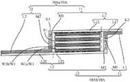
在一些实施例中,如图7所示,显示面板100内,相邻的两条第一扇出线10A中,第一条第一扇出线10Aa的第一直线段L1包括第一部分L11和第二部分L12,第二条第一扇出线10Ab的第二直线段L2包括第三部分L21和第四部分L22。第一部分L11与第二条第一扇出线10Ab的第一直线段L1相邻设置,第二部分L12与第三部分L21相邻设置,第一条第一扇出线10Aa的第二直线段L2与第四部分L22相邻设置。第一部分L11与第二条第一扇出线10Ab的第一直线段L1之间的间距,等于第一条第一扇出线10Aa的第二直线段L2与第四部分L22之间的间距。第二部分L12与第三部分L21之间的间距,大于第一部分L11与第二条第一扇出线10Ab的第一直线段L1之间的间距。In some embodiments, as shown in FIG. 7 , among two adjacent first fan-out
由于为了使得各个扇出线10的长度相等,各个扇出线10的弯折情况由于其位置的不同并不一致。基于此,除最外侧两条扇出线10,其他扇出线10均可以设置不同程度的弯折情况。如图7所示,相邻两条第一扇出线10A均具有弯折区。示例性的,第一直线段L1的延伸方向和第一连接端部M1的延伸方向相交。也即,第一扇出线10A在第一连接端部M1的位置处发生弯折。以保证相邻两条第一扇出线10A的长度相等。In order to make the lengths of the fan-out
如上设置,相邻两条第一扇出线10A之间存在第一容纳空间R1。第一容纳空间R1由第二部分L12、第三部分L21、以及相邻两条第一扇出线10A的第一连接端部M1和第二连接端部M2形成。As set up above, there is a first accommodating space R1 between two adjacent first fan-out
基于此,显示面板100还包括第一虚拟走线结构W1。第一虚拟走线结构W1位于第一容纳空间R1内。也即,第一虚拟走线结构W1位于第二部分L12与第三部分L21之间。Based on this, the
在一些示例中,一部分第一虚拟走线结构W1a与第一走线段11同层、另一部分第一虚拟走线结构W1b与第二走线段12同层。如此设置,可以补偿第一容纳空间R1位置处的刻蚀速率,与第一走线段11和第二走线段12刻蚀速率不同的问题。平衡扇出区F内第一走线段11所在金属层和第二走线段12所在金属层的刻蚀速率。In some examples, a part of the first dummy wiring structure W1a is on the same layer as the
在另一些实施例中,如图7所示,沿第二部分L12指向第三部分L21的方向上,第一虚拟走线结构W1a和第一虚拟走线结构W1b交替设置。由于第一走线段11和第二走线段12也是交替设置的,可以使得相邻第一虚拟走线结构W1a之间的间隙、相邻第一虚拟走线结构W1b之间的间隙、相邻第一走线段11之间的间隙,以及相邻第二走线段12之间的间隙的大致相等,进一步平衡扇出区F内第一走线段11所在金属层和第二走线段12所在金属层的刻蚀速率。In some other embodiments, as shown in FIG. 7 , along the direction from the second portion L12 to the third portion L21 , the first dummy wiring structures W1a and the first dummy wiring structures W1b are arranged alternately. Since the
在一些实施例中,如图5所示,显示面板100中扇出区F内,在第二扇出线10B中,第一走线段11包括第一蛇形走线S1和第三连接端部M3,第二走线段12包括第二蛇形走线S2和第四连接端部M4。显示面板100还包括第二导电连接层Q2,第二导电连接层Q2通过第三过孔K3电连接至第三连接端部M3,且第二导电连接层Q2通过第四过孔K4电连接至第四连接端部M4。In some embodiments, as shown in FIG. 5 , in the fan-out area F of the
第二导电连接层Q2与第一走线段11异层设置,通过第三过孔K3电连接至第三连接端部M3。并且第二导电连接层Q2与第二走线段12异层设置。第二导电连接层Q2通过第四过孔K4电连接至第四连接端部M4。由此实现第一走线段11和第二走线段12电连接。The second conductive connection layer Q2 is arranged in a different layer from the
在一些示例中,显示面板100还包括透明电极层I,透明电极层I位于源漏导电层SD远离栅极导电层G的一侧。第一导电连接层Q1可以位于透明电极层I。第一导电连接层Q1还可以包括像素电极或公共电极。In some examples, the
示例性的,透明电极层的材料可以为氧化铟锡(Indium Tin Oxide,简称ITO),但本公开对此不做限定。Exemplarily, the material of the transparent electrode layer may be indium tin oxide (Indium Tin Oxide, ITO for short), but this disclosure is not limited thereto.
在一些示例中,第二导电连接层Q2通过至少一个第三过孔K3电连接至第三连接端部M3。In some examples, the second conductive connection layer Q2 is electrically connected to the third connection terminal M3 through at least one third via hole K3.
示例性的,第二导电连接层Q2通过一个第三过孔K3电连接至第三连接端部M3。Exemplarily, the second conductive connection layer Q2 is electrically connected to the third connection terminal M3 through a third via hole K3.
当第二导电连接层Q2通过一个第三过孔K3电连接至第三连接端部M3时,可以设置第三过孔K3的尺寸与第二导电连接层Q2的宽度大致相等,只要使得沿垂直第二导电连接层Q2所在平面的方向上,第二导电连接层Q2覆盖第三过孔K3即可,保证可以实现第二导电连接层Q2和第三连接端部M3电连接。此外,设置第三过孔K3的尺寸与第二导电连接层Q2的宽度大致相等,可以增加第二导电连接层Q2和第三连接端部M3的接触面积,降低第二导电连接层Q2和第三连接端部M3的接触电阻,防止第二导电连接层Q2和第三连接端部M3出现搭接不良的问题。When the second conductive connection layer Q2 is electrically connected to the third connection terminal M3 through a third via hole K3, the size of the third via hole K3 can be set to be approximately equal to the width of the second conductive connection layer Q2, as long as the vertical In the direction of the plane where the second conductive connection layer Q2 is located, it is enough that the second conductive connection layer Q2 covers the third via hole K3 to ensure that the second conductive connection layer Q2 and the third connection end M3 can be electrically connected. In addition, setting the size of the third via hole K3 to be approximately equal to the width of the second conductive connection layer Q2 can increase the contact area between the second conductive connection layer Q2 and the third connection end M3, and reduce the contact area between the second conductive connection layer Q2 and the second conductive connection layer Q2. The contact resistance of the three connection ends M3 prevents the problem of poor overlap between the second conductive connection layer Q2 and the third connection end M3.
示例性的,第二导电连接层Q2通过多个第三过孔K3电连接至第三连接端部M3。Exemplarily, the second conductive connection layer Q2 is electrically connected to the third connection terminal M3 through a plurality of third via holes K3.
当第二导电连接层Q2通过多个第三过孔K3电连接至第三连接端部M3时,可以设置多个第三过孔K3沿第三连接端部M3的延伸方向排布,也可以设置多个第三过孔K3沿垂直第三连接端部M3的延伸方向排布,或者,多个第三过孔K3阵列排布。只要使得沿垂直第二导电连接层Q2所在平面的方向上,第二导电连接层Q2覆盖全部第三过孔K3即可,保证可以实现第二导电连接层Q2和第三连接端部M3电连接。此外,设置第二导电连接层Q2通过多个第三过孔K3电连接至第三连接端部M3时,第三过孔K3的直径较小一些,可以有利于降低第三过孔K3的刻蚀工艺难度,提高第二导电连接层Q2和第三连接端部M3的搭接良率。When the second conductive connection layer Q2 is electrically connected to the third connection terminal M3 through a plurality of third via holes K3, a plurality of third via holes K3 may be arranged along the extending direction of the third connection terminal M3, or A plurality of third via holes K3 are arranged along the extending direction perpendicular to the third connecting end portion M3, or a plurality of third via holes K3 are arranged in an array. As long as the second conductive connection layer Q2 covers all the third via holes K3 in the direction perpendicular to the plane where the second conductive connection layer Q2 is located, it is ensured that the second conductive connection layer Q2 and the third connection terminal M3 can be electrically connected. . In addition, when the second conductive connection layer Q2 is set to be electrically connected to the third connection end M3 through a plurality of third via holes K3, the diameter of the third via holes K3 is smaller, which can help reduce the marking of the third via holes K3. The difficulty of the etching process is improved, and the overlapping yield of the second conductive connection layer Q2 and the third connection end M3 is improved.
综上,本公开实施例对第三过孔K3的数量不做具体限定,可以根据实际情况设置。To sum up, the embodiment of the present disclosure does not specifically limit the number of the third via holes K3, which can be set according to actual conditions.
在一些示例中,第二导电连接层Q2通过一个第四过孔K4电连接至第四连接端部M4。In some examples, the second conductive connection layer Q2 is electrically connected to the fourth connection terminal M4 through a fourth via hole K4 .
示例性的,第二导电连接层Q2通过一个第四过孔K4电连接至第四连接端部M4。Exemplarily, the second conductive connection layer Q2 is electrically connected to the fourth connection terminal M4 through a fourth via hole K4.
当第二导电连接层Q2通过一个第四过孔K4电连接至第四连接端部M4时,可以设置第四过孔K4的尺寸与第二导电连接层Q2的宽度大致相等,只要使得沿垂直第二导电连接层Q2所在平面的方向上,第二导电连接层Q2覆盖第四过孔K4即可,保证可以实现第二导电连接层Q2和第四连接端部M4电连接。此外,设置第四过孔K4的尺寸与第二导电连接层Q2的宽度大致相等,可以增加第二导电连接层Q2和第四连接端部M4的接触面积,降低第二导电连接层Q2和第四连接端部M4的接触电阻,防止第二导电连接层Q2和第四连接端部M4出现断路等搭接不良的问题。When the second conductive connection layer Q2 is electrically connected to the fourth connection terminal M4 through a fourth via hole K4, the size of the fourth via hole K4 can be set to be approximately equal to the width of the second conductive connection layer Q2, as long as the vertical In the direction of the plane where the second conductive connection layer Q2 is located, it is enough that the second conductive connection layer Q2 covers the fourth via hole K4 to ensure that the second conductive connection layer Q2 and the fourth connection end M4 can be electrically connected. In addition, setting the size of the fourth via hole K4 to be approximately equal to the width of the second conductive connection layer Q2 can increase the contact area between the second conductive connection layer Q2 and the fourth connection end M4, and reduce the contact area between the second conductive connection layer Q2 and the second conductive connection layer Q2. The contact resistance of the four connection ends M4 prevents problems such as open circuit and poor lap connection between the second conductive connection layer Q2 and the fourth connection end M4.
示例性的,第二导电连接层Q2通过多个第四过孔K4电连接至第四连接端部M4。Exemplarily, the second conductive connection layer Q2 is electrically connected to the fourth connection terminal M4 through a plurality of fourth via holes K4.
当第二导电连接层Q2通过多个第四过孔K4电连接至第四连接端部M4时,可以设置多个第四过孔K4沿第四连接端部M4的延伸方向排布,也可以设置多个第四过孔K4沿垂直第四连接端部M4的延伸方向排布,或者,多个第四过孔K4阵列排布。只要使得沿垂直第二导电连接层Q2所在平面的方向上,第二导电连接层Q2覆盖全部第四过孔K4即可,保证可以实现第二导电连接层Q2和第四连接端部M4电连接。此外,设置第二导电连接层Q2通过多个第四过孔K4电连接至第四连接端部M4时,第四过孔K4的直径较小一些,可以有利于降低第四过孔K4的刻蚀工艺难度,提高第二导电连接层Q2和第四连接端部M4的搭接良率。When the second conductive connection layer Q2 is electrically connected to the fourth connection terminal M4 through a plurality of fourth via holes K4, a plurality of fourth via holes K4 may be arranged along the extending direction of the fourth connection terminal M4, or A plurality of fourth via holes K4 are arranged along the extending direction perpendicular to the fourth connecting end portion M4, or a plurality of fourth via holes K4 are arranged in an array. As long as the second conductive connection layer Q2 covers all the fourth via holes K4 along the direction perpendicular to the plane where the second conductive connection layer Q2 is located, it is ensured that the second conductive connection layer Q2 and the fourth connection terminal M4 can be electrically connected. . In addition, when the second conductive connection layer Q2 is set to be electrically connected to the fourth connection end M4 through a plurality of fourth via holes K4, the diameter of the fourth via holes K4 is smaller, which can help reduce the marking of the fourth via holes K4. The difficulty of the etching process is improved, and the overlapping yield of the second conductive connection layer Q2 and the fourth connection end M4 is improved.
在一些实施例中,如图5所示,显示面板100中在第二扇出线10B中,第一走线段11包括第一蛇形走线S1和第三连接端部M3,第二走线段12包括第二蛇形走线S2和第四连接端部M4。显示面板100还包括第二导电连接层Q2,第二导电连接层Q2通过第三过孔K3电连接至第三连接端部M3,且第二导电连接层Q2通过第四过孔K4电连接至第四连接端部M4。In some embodiments, as shown in FIG. 5 , in the second fan-out
基于此,设置第三连接端部M3的线宽等于第一蛇形走线S1的线宽。和/或,第四连接端部M4的线宽等于第二蛇形走线S2的线宽。Based on this, the line width of the third connection end portion M3 is set to be equal to the line width of the first serpentine line S1. And/or, the line width of the fourth connection end portion M4 is equal to the line width of the second serpentine trace S2.
上述结构可以包括以下几种情况:The above structure can include the following situations:
第一种:如图5所示的第一走线段11。设置第三连接端部M3的线宽等于第一蛇形走线S1的线宽。相当于第一走线段11在任意位置处的宽度均相等。一方面,可以降低工艺难度,简化工艺制程。另一方面,可以节省扇出区F的空间,有利于扇出线10的走线布局。The first type: the
第二种:如图5所示的第二走线段12。第四连接端部M4的线宽等于第二蛇形走线S2的线宽。相当于第二走线段12在任意位置处的宽度均相等。一方面,可以降低工艺难度,简化工艺制程。另一方面,可以节省扇出区F的空间,有利于扇出线10的走线布局。The second type: the
第三种:如图5所示的第一走线段11和第二走线段12。设置第三连接端部M3的线宽等于第一蛇形走线S1的线宽,且第四连接端部M4的线宽等于第二蛇形走线S2的线宽。相当于第一走线段11在任意位置处的宽度均相等,且第二走线段12在任意位置处的宽度均相等。一方面,可以降低工艺难度,简化工艺制程。另一方面,可以节省扇出区F的空间,有利于扇出线10的走线布局。The third type: the
在另一些实施例中,如图6所示,显示面板100中在第二扇出线10B中,第一走线段11包括第一蛇形走线S1和第三连接端部M3,第二走线段12包括第二蛇形走线S2和第四连接端部M4。显示面板100还包括第二导电连接层Q2,第二导电连接层Q2通过第三过孔K3电连接至第三连接端部M3,且第二导电连接层Q2通过第四过孔K4电连接至第四连接端部M4。In other embodiments, as shown in FIG. 6 , in the second fan-out
基于此,设置第三连接端部M3的线宽DM3大于第一蛇形走线S1的线宽DS1。和/或,第四连接端部M4的线宽DM4大于第二蛇形走线S2的线宽DS2。Based on this, the line width DM3 of the third connection end portion M3 is set to be larger than the line width DS1 of the first serpentine trace S1. And/or, the line width DM4 of the fourth connection end portion M4 is larger than the line width DS2 of the second serpentine trace S2.
上述结构可以包括以下几种情况:The above structure can include the following situations:
第一种:如图6所示的第一走线段11。第三连接端部M3的线宽DM3大于第一蛇形走线S1的线宽DS1。The first type: the
第一走线段11通过第三连接端部M3与第二走线段12电连接,设置第三连接端部M3的线宽DM3大于第一蛇形走线S1的线宽DS1,可以增加第一走线段11与第二走线段12电连接位置处的面积。一方面,增大第一走线段11第三连接端部M3的面积,便于设置第三过孔K3,实现第二导电连接层Q2通过第三过孔K3电连接至第三连接端部M3。另一方面,增大第一走线段11第三连接端部M3的面积,可以降低第二导电连接层Q2和第三连接端部M3的接触电阻,防止第二导电连接层Q2和第三连接端部M3出现搭接不良的问题。The
其中,本公开实施例对第三连接端部M3的线宽DM3大于第一蛇形走线S1的线宽DS1的范围不做限定,可以根据扇出区F的空间进行调节设置。Wherein, the embodiment of the present disclosure does not limit the range in which the line width DM3 of the third connection end M3 is greater than the line width DS1 of the first serpentine line S1 , which can be adjusted and set according to the space of the fan-out area F.
第二种:如图6所示的第二走线段12。第四连接端部M4的线宽DM4大于第二蛇形走线S2的线宽DS2。The second type: the
第二走线段12通过第四连接端部M4与第一走线段11电连接,设置第四连接端部M4的线宽DM4大于第二蛇形走线S2的线宽DS2,可以增加第二走线段12与第一走线段11电连接位置处的面积。一方面,增大第二走线段12第四连接端部M4的面积,便于设置第四过孔K4,实现第二导电连接层Q2通过第四过孔K4电连接至第四连接端部M4。另一方面,增大第二走线段12第四连接端部M4的面积,可以降低第二导电连接层Q2和第四连接端部M4的接触电阻,防止第二导电连接层Q2和第四连接端部M4出现搭接不良的问题。The
其中,本公开实施例对第四连接端部M4的线宽DM4大于第二蛇形走线S2的线宽DS2的范围不做限定,可以根据扇出区F的空间进行调节设置。Wherein, the embodiment of the present disclosure does not limit the range in which the line width DM4 of the fourth connection end M4 is greater than the line width DS2 of the second serpentine line S2, and can be adjusted and set according to the space of the fan-out area F.
第三种:如图6所示的第一走线段11和第二走线段12。第三连接端部M3的线宽DM3大于第一蛇形走线S1的线宽DS1,且第四连接端部M4的线宽DM4大于第二蛇形走线S2的线宽DS2。The third type: the
第一走线段11通过第三连接端部M3与第二走线段12通过第二连接端部M2电连接,设置第三连接端部M3的线宽DM3大于第一蛇形走线S1的线宽DS1,且第四连接端部M4的线宽DM4大于第二蛇形走线S2的线宽DS2。可以增大第一走线段11和第二走线段12电连接位置处的面积。既可以便于设置第三过孔K3和第四过孔K4,有利于实现第一走线段11和第二走线段12电连接。还可以降低第一走线段11和第二走线段12的接触电阻,防止第三连接端部M3和第四连接端部M4出现搭接不良的问题。The
其中,本公开实施例对第三连接端部M3的线宽DM3大于第一蛇形走线S1的线宽DS1的范围不做限定;以及,对第四连接端部M4的线宽DM4大于第二蛇形走线S2的线宽DS2的范围不做限定,可以根据扇出区F的空间进行调节设置。Wherein, the embodiment of the present disclosure does not limit the range in which the line width DM3 of the third connection end M3 is greater than the line width DS1 of the first serpentine trace S1; and, the line width DM4 of the fourth connection end M4 is greater than that of the first The range of the line width DS2 of the two serpentine lines S2 is not limited, and can be adjusted and set according to the space of the fan-out area F.
需要说明的是,第一蛇形走线S1的“线宽DS1”为沿垂直第一蛇形走线S1延伸方向上的宽度。第三连接端部M3的“线宽DM3”为沿垂直第三连接端部M3延伸方向上的宽度。第二蛇形走线S2的“线宽DS2”为沿垂直第二蛇形走线S2延伸方向上的宽度。第四连接端部M4的“线宽DM4”为沿垂直第四连接端部M4延伸方向上的宽度。It should be noted that the “line width DS1 ” of the first serpentine trace S1 is the width along the direction perpendicular to the extending direction of the first serpentine trace S1 . The “line width DM3 ” of the third connection end portion M3 is a width along a direction perpendicular to the extending direction of the third connection end portion M3 . The "line width DS2" of the second serpentine trace S2 is the width along the direction perpendicular to the extending direction of the second serpentine trace S2. The “line width DM4 ” of the fourth connection end portion M4 is the width along the direction perpendicular to the extending direction of the fourth connection end portion M4 .
图8为根据一些实施例中提供的相邻的两条第二扇出线和第二虚拟走线结构的位置结构图。Fig. 8 is a position structure diagram of two adjacent second fan-out lines and a second dummy wiring structure according to some embodiments.
在一些实施例中,如图8所示,显示面板100还包括第二虚拟走线结构W2,位于第一蛇形走线S1与第二蛇形走线S2之间。In some embodiments, as shown in FIG. 8 , the
在第一蛇形走线S1与第二蛇形走线S2之间存在第二容纳空间R2。第二容纳空间R2由第一蛇形走线S1、第三连接端部M3、第四连接端部M4、第二蛇形走线S2以及相邻的第二扇出线10B形成。There is a second accommodation space R2 between the first serpentine trace S1 and the second serpentine trace S2. The second accommodation space R2 is formed by the first serpentine wire S1 , the third connection end M3 , the fourth connection end M4 , the second serpentine wire S2 and the adjacent second fan-out
基于此,显示面板100还包括第二虚拟走线结构W2。第二虚拟走线结构W2位于第二容纳空间R2内。也即,第二虚拟走线结构W2位于同一条第二扇出线10B中的第一蛇形走线S1与第二蛇形走线S2之间。Based on this, the
在一些示例中,如图8所示,一部分第二虚拟走线结构W2a与第一走线段11同层、另一部分第二虚拟走线结构W2b与第二走线段12同层。如此设置,可以补偿第二容纳空间R2位置处的刻蚀速率,与第一走线段11和第二走线段12刻蚀速率不同的问题。平衡扇出区F内第一走线段11所在金属层和第二走线段12所在金属层的刻蚀速率。In some examples, as shown in FIG. 8 , a part of the second dummy wiring structure W2 a is on the same layer as the
在另一些实施例中,如图8所示,第二虚拟走线结构W2a与第一走线段11相邻,使得第二虚拟走线结构W2a可以与第一走线段11同步刻蚀。以及,第二虚拟走线结构W2b与第二走线段12相邻,第二虚拟走线结构W2b可以与第二走线段12同步刻蚀。进一步平衡扇出区F内第一走线段11所在金属层和第二走线段12所在金属层的刻蚀速率。In other embodiments, as shown in FIG. 8 , the second dummy wiring structure W2 a is adjacent to the
图9为根据另一些实施例提供的扇出区的结构图。图10为根据又一些实施例提供的扇出区的结构图。Fig. 9 is a structural diagram of a fan-out area provided according to some other embodiments. Fig. 10 is a structural diagram of a fan-out zone provided according to still some embodiments.
在一些实施例中,如图9和图10所示,显示面板100中在第一扇出线10A中,第一走线段11包括第一直线段L1和第一连接端部M1,第二走线段12包括第二直线段L2和第二连接端部M2。沿垂直第一走线段11所在金属层的方向上,第一连接端部M1和第二连接端部M2至少部分交叠,在该交叠部分处,第一连接端部M1和第二连接端部M2通过第五过孔K5电连接。In some embodiments, as shown in FIG. 9 and FIG. 10, in the first fan-out
对于第五过孔K5的形状、大小、数量不做具体限定,可以根据实际情况设置。The shape, size, and quantity of the fifth via hole K5 are not specifically limited, and may be set according to actual conditions.
图11为根据另一些实施例提供的显示面板的结构图。图12为根据一些实施例提供的静电屏蔽电路的电路图。Fig. 11 is a structural diagram of a display panel provided according to other embodiments. 12 is a circuit diagram of an electrostatic shielding circuit provided according to some embodiments.
在一些实施例中,如图11和图12所示,显示面板100还包括多个静电屏蔽电路ESD。多个静电屏蔽电路ESD中,一个静电屏蔽电路ESD与至少一条扇出线10电连接。In some embodiments, as shown in FIG. 11 and FIG. 12 , the
如图12所示,静电屏蔽电路ESD包括四个晶体管:第一晶体管T1、第二晶体管T2、第三晶体管T3和第四晶体管T4。As shown in FIG. 12 , the electrostatic shielding circuit ESD includes four transistors: a first transistor T1 , a second transistor T2 , a third transistor T3 and a fourth transistor T4 .
第一晶体管T1的第一极和控制极电连接至扇出线10,第一晶体管T1的第二极电连接至第三晶体管T3的控制极和第一极。The first electrode and the control electrode of the first transistor T1 are electrically connected to the fan-out
第二晶体管T2的第一极电连接至扇出线10,第二晶体管T2的控制极和第二极电连接至第四晶体管T4的第一极。The first pole of the second transistor T2 is electrically connected to the fan-out
第三晶体管T3的第一极和第四晶体管T4的第一极电连接,第三晶体管T3的第二极电连接至公共层COM。The first electrode of the third transistor T3 is electrically connected to the first electrode of the fourth transistor T4, and the second electrode of the third transistor T3 is electrically connected to the common layer COM.
第四晶体管T4的控制极和第二极电连接至公共层COM。The control electrode and the second electrode of the fourth transistor T4 are electrically connected to the common layer COM.
基于此,在扇出线10流经大电流时,大电流流经静电屏蔽电路ESD,并通过公共层COM导出,避免扇出线10将其导入至显示面板100内的数据线DL内,影响显示面板100的显示效果。Based on this, when the fan-out
在另一些实施例中,静电屏蔽电路ESD可以是TVS(Transient VoltageSuppresser,瞬态电压抑制器)管、压敏电阻、稳压二极管以及ESD保护电路等中的任意一种或多种,本实施例对ESD保护器件的具体类型并不加以限制,也不局限于上述示例。In some other embodiments, the electrostatic shielding circuit ESD may be any one or more of TVS (Transient Voltage Suppresser, transient voltage suppressor) tube, varistor, Zener diode, and ESD protection circuit. The specific types of ESD protection devices are not limited, nor are they limited to the above examples.
以上所述,仅为本公开的具体实施方式,但本公开的保护范围并不局限于此,任何熟悉本技术领域的技术人员在本公开揭露的技术范围内,想到变化或替换,都应涵盖在本公开的保护范围之内。因此,本公开的保护范围应以所述权利要求的保护范围为准。The above is only a specific embodiment of the present disclosure, but the scope of protection of the present disclosure is not limited thereto. Anyone familiar with the technical field who thinks of changes or substitutions within the technical scope of the present disclosure should cover all within the protection scope of the present disclosure. Therefore, the protection scope of the present disclosure should be determined by the protection scope of the claims.
Claims (13)
Translated fromChinesePriority Applications (1)
| Application Number | Priority Date | Filing Date | Title |
|---|---|---|---|
| CN202210973372.7ACN115308957B (en) | 2022-08-15 | 2022-08-15 | Display panels and display devices |
Applications Claiming Priority (1)
| Application Number | Priority Date | Filing Date | Title |
|---|---|---|---|
| CN202210973372.7ACN115308957B (en) | 2022-08-15 | 2022-08-15 | Display panels and display devices |
Publications (2)
| Publication Number | Publication Date |
|---|---|
| CN115308957Atrue CN115308957A (en) | 2022-11-08 |
| CN115308957B CN115308957B (en) | 2024-03-22 |
Family
ID=83862263
Family Applications (1)
| Application Number | Title | Priority Date | Filing Date |
|---|---|---|---|
| CN202210973372.7AActiveCN115308957B (en) | 2022-08-15 | 2022-08-15 | Display panels and display devices |
Country Status (1)
| Country | Link |
|---|---|
| CN (1) | CN115308957B (en) |
Cited By (2)
| Publication number | Priority date | Publication date | Assignee | Title |
|---|---|---|---|---|
| CN118335754A (en)* | 2024-06-12 | 2024-07-12 | 惠科股份有限公司 | Array substrate and electronic paper display panel |
| WO2024182965A1 (en)* | 2023-03-06 | 2024-09-12 | 京东方科技集团股份有限公司 | Array substrate and display apparatus |
Citations (13)
| Publication number | Priority date | Publication date | Assignee | Title |
|---|---|---|---|---|
| JP2003257971A (en)* | 2002-02-27 | 2003-09-12 | Seiko Epson Corp | Semiconductor device |
| US20060049151A1 (en)* | 2004-09-03 | 2006-03-09 | Lee Yong H | Plasma display apparatus including electrode pad |
| KR20070016088A (en)* | 2005-08-02 | 2007-02-07 | 산요 엡슨 이미징 디바이스 가부시키가이샤 | Electro-optical devices and electronics |
| US20080079859A1 (en)* | 2006-09-28 | 2008-04-03 | Epson Imaging Devices Corporation | Liquid crystal display panel |
| CN106707646A (en)* | 2017-02-07 | 2017-05-24 | 厦门天马微电子有限公司 | Array base plate and display panel |
| CN206301112U (en)* | 2016-10-18 | 2017-07-04 | 京东方科技集团股份有限公司 | A kind of array substrate and display device |
| US20170192279A1 (en)* | 2016-01-05 | 2017-07-06 | Japan Display Inc. | Display device |
| CN107479275A (en)* | 2017-08-08 | 2017-12-15 | 惠科股份有限公司 | Display panel and display device |
| CN110412802A (en)* | 2019-06-27 | 2019-11-05 | 厦门天马微电子有限公司 | Display panel and display device |
| CN210092083U (en)* | 2019-03-20 | 2020-02-18 | 咸阳彩虹光电科技有限公司 | Fan-out area wiring structure |
| US20220069052A1 (en)* | 2020-08-28 | 2022-03-03 | Boe Technology Group Co., Ltd. | Display panel and display device |
| CN114497118A (en)* | 2020-10-23 | 2022-05-13 | 京东方科技集团股份有限公司 | Display substrate, preparation method thereof and display device |
| CN114721193A (en)* | 2022-04-21 | 2022-07-08 | 滁州惠科光电科技有限公司 | Array substrate and display panel |
- 2022
- 2022-08-15CNCN202210973372.7Apatent/CN115308957B/enactiveActive
Patent Citations (13)
| Publication number | Priority date | Publication date | Assignee | Title |
|---|---|---|---|---|
| JP2003257971A (en)* | 2002-02-27 | 2003-09-12 | Seiko Epson Corp | Semiconductor device |
| US20060049151A1 (en)* | 2004-09-03 | 2006-03-09 | Lee Yong H | Plasma display apparatus including electrode pad |
| KR20070016088A (en)* | 2005-08-02 | 2007-02-07 | 산요 엡슨 이미징 디바이스 가부시키가이샤 | Electro-optical devices and electronics |
| US20080079859A1 (en)* | 2006-09-28 | 2008-04-03 | Epson Imaging Devices Corporation | Liquid crystal display panel |
| US20170192279A1 (en)* | 2016-01-05 | 2017-07-06 | Japan Display Inc. | Display device |
| CN206301112U (en)* | 2016-10-18 | 2017-07-04 | 京东方科技集团股份有限公司 | A kind of array substrate and display device |
| CN106707646A (en)* | 2017-02-07 | 2017-05-24 | 厦门天马微电子有限公司 | Array base plate and display panel |
| CN107479275A (en)* | 2017-08-08 | 2017-12-15 | 惠科股份有限公司 | Display panel and display device |
| CN210092083U (en)* | 2019-03-20 | 2020-02-18 | 咸阳彩虹光电科技有限公司 | Fan-out area wiring structure |
| CN110412802A (en)* | 2019-06-27 | 2019-11-05 | 厦门天马微电子有限公司 | Display panel and display device |
| US20220069052A1 (en)* | 2020-08-28 | 2022-03-03 | Boe Technology Group Co., Ltd. | Display panel and display device |
| CN114497118A (en)* | 2020-10-23 | 2022-05-13 | 京东方科技集团股份有限公司 | Display substrate, preparation method thereof and display device |
| CN114721193A (en)* | 2022-04-21 | 2022-07-08 | 滁州惠科光电科技有限公司 | Array substrate and display panel |
Cited By (3)
| Publication number | Priority date | Publication date | Assignee | Title |
|---|---|---|---|---|
| WO2024182965A1 (en)* | 2023-03-06 | 2024-09-12 | 京东方科技集团股份有限公司 | Array substrate and display apparatus |
| CN118335754A (en)* | 2024-06-12 | 2024-07-12 | 惠科股份有限公司 | Array substrate and electronic paper display panel |
| CN118335754B (en)* | 2024-06-12 | 2024-10-11 | 惠科股份有限公司 | Array substrate and electronic paper display panel |
Also Published As
| Publication number | Publication date |
|---|---|
| CN115308957B (en) | 2024-03-22 |
Similar Documents
| Publication | Publication Date | Title |
|---|---|---|
| US6919591B2 (en) | Thin film transistor array panel for a liquid crystal display | |
| US9703150B2 (en) | Liquid crystal display device | |
| US7777823B2 (en) | Thin film transistor array panel | |
| CN115308957B (en) | Display panels and display devices | |
| CN109686757B (en) | Flexible substrate and display panel using the same | |
| CN111948859B (en) | Display substrate and display device | |
| CN114280868A (en) | Display substrate, display panel and display device | |
| US11573468B2 (en) | Display substrate including a multi-layer structure of an organic layer and an inorganic layer, display device having the same, and method of manufacturing the display substrate | |
| US11048133B2 (en) | Liquid crystal display panel and liquid crystal display device including the same | |
| CN115715132A (en) | Display device | |
| CN108376684B (en) | display panel | |
| KR20180031898A (en) | Display device having common voltage line | |
| CN112147824A (en) | Array substrate, manufacturing method thereof and display device | |
| KR101433935B1 (en) | Display panel and manufacturing method of display substrate | |
| US11340503B2 (en) | Display device | |
| US12225791B2 (en) | Display module and vehicle display apparatus | |
| US20190025659A1 (en) | Display device | |
| US11960177B2 (en) | Display device | |
| US11537013B2 (en) | Display panel and display device | |
| US12437684B2 (en) | Display panel and display device | |
| US12399406B2 (en) | Display panel, display device | |
| US20250113614A1 (en) | Array substrate, display panel and display device | |
| US20240284729A1 (en) | Array substrate, display apparatus, and method of fabricating array substrate | |
| JP2008185801A (en) | Electro-optical device manufacturing method, electro-optical device, and electronic apparatus | |
| CN117590637A (en) | Liquid crystal display panel and display device |
Legal Events
| Date | Code | Title | Description |
|---|---|---|---|
| PB01 | Publication | ||
| PB01 | Publication | ||
| SE01 | Entry into force of request for substantive examination | ||
| SE01 | Entry into force of request for substantive examination | ||
| GR01 | Patent grant | ||
| GR01 | Patent grant |