CN115280135A - Nucleic acid sequencing cassettes, packaging devices and systems - Google Patents
Nucleic acid sequencing cassettes, packaging devices and systemsDownload PDFInfo
- Publication number
- CN115280135A CN115280135ACN202180020758.XACN202180020758ACN115280135ACN 115280135 ACN115280135 ACN 115280135ACN 202180020758 ACN202180020758 ACN 202180020758ACN 115280135 ACN115280135 ACN 115280135A
- Authority
- CN
- China
- Prior art keywords
- nucleic acid
- acid sequencing
- flow cell
- optical
- cartridge
- Prior art date
- Legal status (The legal status is an assumption and is not a legal conclusion. Google has not performed a legal analysis and makes no representation as to the accuracy of the status listed.)
- Pending
Links
- 238000012163sequencing techniqueMethods0.000titleclaimsabstractdescription283
- 150000007523nucleic acidsChemical class0.000titleclaimsabstractdescription248
- 102000039446nucleic acidsHuman genes0.000titleclaimsabstractdescription248
- 108020004707nucleic acidsProteins0.000titleclaimsabstractdescription248
- 238000004806packaging method and processMethods0.000titleclaimsabstractdescription99
- 230000003287optical effectEffects0.000claimsabstractdescription397
- 238000006243chemical reactionMethods0.000claimsabstractdescription196
- 238000004458analytical methodMethods0.000claimsabstractdescription61
- 230000001681protective effectEffects0.000claimsabstractdescription48
- 230000002441reversible effectEffects0.000claimsabstractdescription6
- 239000012530fluidSubstances0.000claimsdescription154
- 239000000463materialSubstances0.000claimsdescription68
- 229920003023plasticPolymers0.000claimsdescription49
- 230000005284excitationEffects0.000claimsdescription35
- 239000004033plasticSubstances0.000claimsdescription30
- 238000001816coolingMethods0.000claimsdescription21
- 239000000853adhesiveSubstances0.000claimsdescription20
- 230000001070adhesive effectEffects0.000claimsdescription20
- 230000005855radiationEffects0.000claimsdescription18
- 239000002470thermal conductorSubstances0.000claimsdescription17
- 230000007246mechanismEffects0.000claimsdescription16
- 229920000122acrylonitrile butadiene styrenePolymers0.000claimsdescription12
- 239000003973paintSubstances0.000claimsdescription10
- 239000004676acrylonitrile butadiene styreneSubstances0.000claimsdescription9
- XECAHXYUAAWDEL-UHFFFAOYSA-Nacrylonitrile butadiene styreneChemical compoundC=CC=C.C=CC#N.C=CC1=CC=CC=C1XECAHXYUAAWDEL-UHFFFAOYSA-N0.000claimsdescription8
- 239000006260foamSubstances0.000claimsdescription7
- XUIMIQQOPSSXEZ-UHFFFAOYSA-NSiliconChemical compound[Si]XUIMIQQOPSSXEZ-UHFFFAOYSA-N0.000claimsdescription6
- 238000001465metallisationMethods0.000claimsdescription6
- 239000011148porous materialSubstances0.000claimsdescription6
- 230000001443photoexcitationEffects0.000claimsdescription5
- 229910052710siliconInorganic materials0.000claimsdescription5
- 239000010703siliconSubstances0.000claimsdescription5
- 239000012780transparent materialSubstances0.000claimsdescription4
- 239000003153chemical reaction reagentSubstances0.000abstractdescription40
- 238000003556assayMethods0.000abstractdescription12
- 210000004027cellAnatomy0.000description214
- 239000000523sampleSubstances0.000description163
- 238000000034methodMethods0.000description87
- 125000003729nucleotide groupChemical group0.000description48
- 239000002773nucleotideSubstances0.000description46
- 238000011068loading methodMethods0.000description32
- 239000007788liquidSubstances0.000description21
- 238000005286illuminationMethods0.000description20
- 239000000758substrateSubstances0.000description17
- 230000008901benefitEffects0.000description15
- 230000008569processEffects0.000description15
- 238000013461designMethods0.000description13
- 238000001514detection methodMethods0.000description12
- 230000008878couplingEffects0.000description10
- 238000010168coupling processMethods0.000description10
- 238000005859coupling reactionMethods0.000description10
- 230000002829reductive effectEffects0.000description10
- 239000013307optical fiberSubstances0.000description9
- 239000000376reactantSubstances0.000description9
- 239000011888foilSubstances0.000description7
- 238000010348incorporationMethods0.000description7
- 238000003780insertionMethods0.000description7
- 230000037431insertionEffects0.000description7
- 150000003071polychlorinated biphenylsChemical class0.000description7
- 239000000126substanceSubstances0.000description7
- VYPSYNLAJGMNEJ-UHFFFAOYSA-NSilicium dioxideChemical compoundO=[Si]=OVYPSYNLAJGMNEJ-UHFFFAOYSA-N0.000description6
- 238000003491arrayMethods0.000description6
- 239000000835fiberSubstances0.000description6
- 239000012634fragmentSubstances0.000description6
- 238000012351Integrated analysisMethods0.000description5
- 230000005540biological transmissionEffects0.000description5
- 239000011248coating agentSubstances0.000description5
- 238000000576coating methodMethods0.000description5
- 239000007850fluorescent dyeSubstances0.000description5
- 239000007789gasSubstances0.000description5
- 229910052814silicon oxideInorganic materials0.000description5
- 239000000243solutionSubstances0.000description5
- 239000004696Poly ether ether ketoneSubstances0.000description4
- 238000013459approachMethods0.000description4
- 238000004891communicationMethods0.000description4
- 238000010586diagramMethods0.000description4
- 238000005516engineering processMethods0.000description4
- 238000011049fillingMethods0.000description4
- 230000006870functionEffects0.000description4
- 239000011521glassSubstances0.000description4
- 239000000203mixtureSubstances0.000description4
- 229920002530polyetherether ketonePolymers0.000description4
- 238000012545processingMethods0.000description4
- 230000035945sensitivityEffects0.000description4
- 238000012546transferMethods0.000description4
- 238000001712DNA sequencingMethods0.000description3
- 230000027455bindingEffects0.000description3
- 238000004061bleachingMethods0.000description3
- 230000000295complement effectEffects0.000description3
- 238000011109contaminationMethods0.000description3
- 230000000875corresponding effectEffects0.000description3
- 238000005259measurementMethods0.000description3
- 238000002156mixingMethods0.000description3
- 239000002245particleSubstances0.000description3
- 229920000139polyethylene terephthalatePolymers0.000description3
- 239000005020polyethylene terephthalateSubstances0.000description3
- 230000009467reductionEffects0.000description3
- 238000010992refluxMethods0.000description3
- 238000011160researchMethods0.000description3
- 238000007789sealingMethods0.000description3
- 230000003595spectral effectEffects0.000description3
- YBJHBAHKTGYVGT-ZKWXMUAHSA-N(+)-BiotinChemical compoundN1C(=O)N[C@@H]2[C@H](CCCCC(=O)O)SC[C@@H]21YBJHBAHKTGYVGT-ZKWXMUAHSA-N0.000description2
- IJGRMHOSHXDMSA-UHFFFAOYSA-NAtomic nitrogenChemical compoundN#NIJGRMHOSHXDMSA-UHFFFAOYSA-N0.000description2
- 102100030569Nuclear receptor corepressor 2Human genes0.000description2
- 101710153660Nuclear receptor corepressor 2Proteins0.000description2
- OIRDTQYFTABQOQ-KQYNXXCUSA-NadenosineChemical compoundC1=NC=2C(N)=NC=NC=2N1[C@@H]1O[C@H](CO)[C@@H](O)[C@H]1OOIRDTQYFTABQOQ-KQYNXXCUSA-N0.000description2
- 230000004075alterationEffects0.000description2
- 230000004888barrier functionEffects0.000description2
- 239000011324beadSubstances0.000description2
- 238000005253claddingMethods0.000description2
- 229910021419crystalline siliconInorganic materials0.000description2
- 238000001723curingMethods0.000description2
- 230000007812deficiencyEffects0.000description2
- 239000000428dustSubstances0.000description2
- 230000000694effectsEffects0.000description2
- 229920001971elastomerPolymers0.000description2
- 238000012921fluorescence analysisMethods0.000description2
- 238000011010flushing procedureMethods0.000description2
- 239000003292glueSubstances0.000description2
- 230000006872improvementEffects0.000description2
- 238000002955isolationMethods0.000description2
- 238000002372labellingMethods0.000description2
- 230000004807localizationEffects0.000description2
- 238000012423maintenanceMethods0.000description2
- 238000004519manufacturing processMethods0.000description2
- 229910052751metalInorganic materials0.000description2
- 239000002184metalSubstances0.000description2
- 229910044991metal oxideInorganic materials0.000description2
- 150000004706metal oxidesChemical class0.000description2
- 238000004204optical analysis methodMethods0.000description2
- 230000003134recirculating effectEffects0.000description2
- 239000004065semiconductorSubstances0.000description2
- 238000000926separation methodMethods0.000description2
- 229910002027silica gelInorganic materials0.000description2
- 239000000741silica gelSubstances0.000description2
- 239000000377silicon dioxideSubstances0.000description2
- 235000012239silicon dioxideNutrition0.000description2
- 239000007787solidSubstances0.000description2
- 238000003860storageMethods0.000description2
- 238000001757thermogravimetry curveMethods0.000description2
- 238000005406washingMethods0.000description2
- 208000032484Accidental exposure to productDiseases0.000description1
- 239000002126C01EB10 - AdenosineSubstances0.000description1
- 206010010071ComaDiseases0.000description1
- RYGMFSIKBFXOCR-UHFFFAOYSA-NCopperChemical compound[Cu]RYGMFSIKBFXOCR-UHFFFAOYSA-N0.000description1
- 239000004593EpoxySubstances0.000description1
- DGAQECJNVWCQMB-PUAWFVPOSA-MIlexoside XXIXChemical compoundC[C@@H]1CC[C@@]2(CC[C@@]3(C(=CC[C@H]4[C@]3(CC[C@@H]5[C@@]4(CC[C@@H](C5(C)C)OS(=O)(=O)[O-])C)C)[C@@H]2[C@]1(C)O)C)C(=O)O[C@H]6[C@@H]([C@H]([C@@H]([C@H](O6)CO)O)O)O.[Na+]DGAQECJNVWCQMB-PUAWFVPOSA-M0.000description1
- 239000004793PolystyreneSubstances0.000description1
- 238000003559RNA-seq methodMethods0.000description1
- 238000003848UV Light-CuringMethods0.000description1
- 231100000818accidental exposureToxicity0.000description1
- 238000009825accumulationMethods0.000description1
- NIXOWILDQLNWCW-UHFFFAOYSA-Nacrylic acid groupChemical groupC(C=C)(=O)ONIXOWILDQLNWCW-UHFFFAOYSA-N0.000description1
- 230000006978adaptationEffects0.000description1
- 229960005305adenosineDrugs0.000description1
- 201000009310astigmatismDiseases0.000description1
- QVGXLLKOCUKJST-UHFFFAOYSA-Natomic oxygenChemical compound[O]QVGXLLKOCUKJST-UHFFFAOYSA-N0.000description1
- 108010058966bacteriophage T7 induced DNA polymeraseProteins0.000description1
- 230000009286beneficial effectEffects0.000description1
- 230000015572biosynthetic processEffects0.000description1
- 229960002685biotinDrugs0.000description1
- 235000020958biotinNutrition0.000description1
- 239000011616biotinSubstances0.000description1
- 230000000903blocking effectEffects0.000description1
- 238000005251capillar electrophoresisMethods0.000description1
- 230000015556catabolic processEffects0.000description1
- 210000003850cellular structureAnatomy0.000description1
- 239000000919ceramicSubstances0.000description1
- 230000008859changeEffects0.000description1
- 238000004140cleaningMethods0.000description1
- 229910052681coesiteInorganic materials0.000description1
- 238000010668complexation reactionMethods0.000description1
- 238000009833condensationMethods0.000description1
- 230000005494condensationEffects0.000description1
- 239000004020conductorSubstances0.000description1
- 239000000356contaminantSubstances0.000description1
- 230000001276controlling effectEffects0.000description1
- 229910052802copperInorganic materials0.000description1
- 239000010949copperSubstances0.000description1
- 230000002596correlated effectEffects0.000description1
- 238000010219correlation analysisMethods0.000description1
- 229910052906cristobaliteInorganic materials0.000description1
- 238000012864cross contaminationMethods0.000description1
- 230000002950deficientEffects0.000description1
- 238000006731degradation reactionMethods0.000description1
- 238000007791dehumidificationMethods0.000description1
- 238000002716delivery methodMethods0.000description1
- 230000001419dependent effectEffects0.000description1
- 238000005137deposition processMethods0.000description1
- 230000023077detection of light stimulusEffects0.000description1
- 230000001627detrimental effectEffects0.000description1
- 238000009826distributionMethods0.000description1
- 239000000806elastomerSubstances0.000description1
- 238000004049embossingMethods0.000description1
- 238000000295emission spectrumMethods0.000description1
- 230000002349favourable effectEffects0.000description1
- 239000010408filmSubstances0.000description1
- 238000001914filtrationMethods0.000description1
- 229920002457flexible plasticPolymers0.000description1
- 239000004811fluoropolymerSubstances0.000description1
- 229920002313fluoropolymerPolymers0.000description1
- 239000000383hazardous chemicalSubstances0.000description1
- 230000002209hydrophobic effectEffects0.000description1
- 229910052738indiumInorganic materials0.000description1
- APFVFJFRJDLVQX-UHFFFAOYSA-Nindium atomChemical compound[In]APFVFJFRJDLVQX-UHFFFAOYSA-N0.000description1
- 238000002347injectionMethods0.000description1
- 239000007924injectionSubstances0.000description1
- 230000010354integrationEffects0.000description1
- 230000003993interactionEffects0.000description1
- 238000010147laser engravingMethods0.000description1
- 230000000670limiting effectEffects0.000description1
- 239000011159matrix materialSubstances0.000description1
- 230000001404mediated effectEffects0.000description1
- 239000012528membraneSubstances0.000description1
- 239000002480mineral oilSubstances0.000description1
- 235000010446mineral oilNutrition0.000description1
- 238000012986modificationMethods0.000description1
- 230000004048modificationEffects0.000description1
- 230000009149molecular bindingEffects0.000description1
- 229910052757nitrogenInorganic materials0.000description1
- 238000003499nucleic acid arrayMethods0.000description1
- 239000003921oilSubstances0.000description1
- 238000005457optimizationMethods0.000description1
- 239000001301oxygenSubstances0.000description1
- 229910052760oxygenInorganic materials0.000description1
- 230000037361pathwayEffects0.000description1
- 125000002467phosphate groupChemical group[H]OP(=O)(O[H])O[*]0.000description1
- 229920002120photoresistant polymerPolymers0.000description1
- 230000000704physical effectEffects0.000description1
- 229920000052poly(p-xylylene)Polymers0.000description1
- -1polyethylene terephthalatePolymers0.000description1
- 238000006116polymerization reactionMethods0.000description1
- 229920002223polystyrenePolymers0.000description1
- 230000036316preloadEffects0.000description1
- 230000037452primingEffects0.000description1
- 238000007639printingMethods0.000description1
- 230000001902propagating effectEffects0.000description1
- 238000000159protein binding assayMethods0.000description1
- 238000005086pumpingMethods0.000description1
- 238000010926purgeMethods0.000description1
- 238000006862quantum yield reactionMethods0.000description1
- 238000009419refurbishmentMethods0.000description1
- 230000001105regulatory effectEffects0.000description1
- 230000008439repair processEffects0.000description1
- 230000004044responseEffects0.000description1
- 230000000717retained effectEffects0.000description1
- 238000007480sanger sequencingMethods0.000description1
- 238000007493shaping processMethods0.000description1
- 230000007781signaling eventEffects0.000description1
- 238000004557single molecule detectionMethods0.000description1
- 229910052708sodiumInorganic materials0.000description1
- 239000011734sodiumSubstances0.000description1
- 238000005476solderingMethods0.000description1
- 239000002904solventSubstances0.000description1
- 125000006850spacer groupChemical group0.000description1
- 230000003068static effectEffects0.000description1
- 229910052682stishoviteInorganic materials0.000description1
- 238000004381surface treatmentMethods0.000description1
- 239000010409thin filmSubstances0.000description1
- 238000002834transmittanceMethods0.000description1
- 229910052905tridymiteInorganic materials0.000description1
- 238000009736wettingMethods0.000description1
Images


Classifications
- G—PHYSICS
- G01—MEASURING; TESTING
- G01N—INVESTIGATING OR ANALYSING MATERIALS BY DETERMINING THEIR CHEMICAL OR PHYSICAL PROPERTIES
- G01N21/00—Investigating or analysing materials by the use of optical means, i.e. using sub-millimetre waves, infrared, visible or ultraviolet light
- G01N21/62—Systems in which the material investigated is excited whereby it emits light or causes a change in wavelength of the incident light
- G01N21/63—Systems in which the material investigated is excited whereby it emits light or causes a change in wavelength of the incident light optically excited
- G01N21/64—Fluorescence; Phosphorescence
- G01N21/645—Specially adapted constructive features of fluorimeters
- G01N21/648—Specially adapted constructive features of fluorimeters using evanescent coupling or surface plasmon coupling for the excitation of fluorescence
- G—PHYSICS
- G01—MEASURING; TESTING
- G01N—INVESTIGATING OR ANALYSING MATERIALS BY DETERMINING THEIR CHEMICAL OR PHYSICAL PROPERTIES
- G01N21/00—Investigating or analysing materials by the use of optical means, i.e. using sub-millimetre waves, infrared, visible or ultraviolet light
- G01N21/62—Systems in which the material investigated is excited whereby it emits light or causes a change in wavelength of the incident light
- G01N21/63—Systems in which the material investigated is excited whereby it emits light or causes a change in wavelength of the incident light optically excited
- G01N21/64—Fluorescence; Phosphorescence
- G01N21/645—Specially adapted constructive features of fluorimeters
- G01N21/6452—Individual samples arranged in a regular 2D-array, e.g. multiwell plates
- G—PHYSICS
- G01—MEASURING; TESTING
- G01N—INVESTIGATING OR ANALYSING MATERIALS BY DETERMINING THEIR CHEMICAL OR PHYSICAL PROPERTIES
- G01N21/00—Investigating or analysing materials by the use of optical means, i.e. using sub-millimetre waves, infrared, visible or ultraviolet light
- G01N21/62—Systems in which the material investigated is excited whereby it emits light or causes a change in wavelength of the incident light
- G01N21/63—Systems in which the material investigated is excited whereby it emits light or causes a change in wavelength of the incident light optically excited
- G01N21/64—Fluorescence; Phosphorescence
- G01N21/6428—Measuring fluorescence of fluorescent products of reactions or of fluorochrome labelled reactive substances, e.g. measuring quenching effects, using measuring "optrodes"
- G—PHYSICS
- G01—MEASURING; TESTING
- G01N—INVESTIGATING OR ANALYSING MATERIALS BY DETERMINING THEIR CHEMICAL OR PHYSICAL PROPERTIES
- G01N21/00—Investigating or analysing materials by the use of optical means, i.e. using sub-millimetre waves, infrared, visible or ultraviolet light
- G01N21/62—Systems in which the material investigated is excited whereby it emits light or causes a change in wavelength of the incident light
- G01N21/63—Systems in which the material investigated is excited whereby it emits light or causes a change in wavelength of the incident light optically excited
- G01N21/64—Fluorescence; Phosphorescence
- G01N21/645—Specially adapted constructive features of fluorimeters
- G01N21/6452—Individual samples arranged in a regular 2D-array, e.g. multiwell plates
- G01N21/6454—Individual samples arranged in a regular 2D-array, e.g. multiwell plates using an integrated detector array
- B—PERFORMING OPERATIONS; TRANSPORTING
- B01—PHYSICAL OR CHEMICAL PROCESSES OR APPARATUS IN GENERAL
- B01L—CHEMICAL OR PHYSICAL LABORATORY APPARATUS FOR GENERAL USE
- B01L3/00—Containers or dishes for laboratory use, e.g. laboratory glassware; Droppers
- B01L3/50—Containers for the purpose of retaining a material to be analysed, e.g. test tubes
- B01L3/502—Containers for the purpose of retaining a material to be analysed, e.g. test tubes with fluid transport, e.g. in multi-compartment structures
- B01L3/5027—Containers for the purpose of retaining a material to be analysed, e.g. test tubes with fluid transport, e.g. in multi-compartment structures by integrated microfluidic structures, i.e. dimensions of channels and chambers are such that surface tension forces are important, e.g. lab-on-a-chip
- B01L3/502715—Containers for the purpose of retaining a material to be analysed, e.g. test tubes with fluid transport, e.g. in multi-compartment structures by integrated microfluidic structures, i.e. dimensions of channels and chambers are such that surface tension forces are important, e.g. lab-on-a-chip characterised by interfacing components, e.g. fluidic, electrical, optical or mechanical interfaces
- G—PHYSICS
- G01—MEASURING; TESTING
- G01N—INVESTIGATING OR ANALYSING MATERIALS BY DETERMINING THEIR CHEMICAL OR PHYSICAL PROPERTIES
- G01N21/00—Investigating or analysing materials by the use of optical means, i.e. using sub-millimetre waves, infrared, visible or ultraviolet light
- G01N21/62—Systems in which the material investigated is excited whereby it emits light or causes a change in wavelength of the incident light
- G01N21/63—Systems in which the material investigated is excited whereby it emits light or causes a change in wavelength of the incident light optically excited
- G01N21/64—Fluorescence; Phosphorescence
- G01N2021/6417—Spectrofluorimetric devices
- G01N2021/6421—Measuring at two or more wavelengths
- G—PHYSICS
- G01—MEASURING; TESTING
- G01N—INVESTIGATING OR ANALYSING MATERIALS BY DETERMINING THEIR CHEMICAL OR PHYSICAL PROPERTIES
- G01N2201/00—Features of devices classified in G01N21/00
- G01N2201/08—Optical fibres; light guides
- G01N2201/0873—Using optically integrated constructions
Landscapes
- Health & Medical Sciences (AREA)
- Chemical & Material Sciences (AREA)
- Immunology (AREA)
- Physics & Mathematics (AREA)
- General Physics & Mathematics (AREA)
- Analytical Chemistry (AREA)
- Biochemistry (AREA)
- General Health & Medical Sciences (AREA)
- Life Sciences & Earth Sciences (AREA)
- Nuclear Medicine, Radiotherapy & Molecular Imaging (AREA)
- Pathology (AREA)
- Chemical Kinetics & Catalysis (AREA)
- Optics & Photonics (AREA)
- Apparatus Associated With Microorganisms And Enzymes (AREA)
- Investigating, Analyzing Materials By Fluorescence Or Luminescence (AREA)
- Measuring Or Testing Involving Enzymes Or Micro-Organisms (AREA)
Abstract
Description
Translated fromChinese相关申请的交叉引用Cross References to Related Applications
本申请要求在2020年1月14日提交的申请号为62/961,175的美国临时申请的权益,上述申请的公开内容通过引用全部并入本文。This application claims the benefit of U.S. Provisional Application No. 62/961,175, filed January 14, 2020, the disclosure of which is incorporated herein by reference in its entirety.
关于联邦资助研究的声明Statement Regarding Federally Funded Research
尚未获得。Not yet available.
背景技术Background technique
随着复用分析系统持续地尺寸小型化、规模扩大和功率增加,开发能够实现这种功能的改进的系统的需求变得更加重要。此外,许多分析技术最初仅以高成本获得,并且它们仅可以由受过高度训练的实验室技术人员在实验室环境中进行。例如,使用昂贵且实施复杂的技术和设备的核酸测序最初仅在研究实验室中是可能的。核酸测序技术的进步已经降低了每单位测序的成本,因此极大地扩大了序列数据的可用性,但是测序反应仍然必须通常由经过高度训练的个体在拥有昂贵设备的复杂实验室中进行。As multiplexed analysis systems continue to be miniaturized, scaled up, and increased in power, the need to develop improved systems capable of such functionality becomes even more important. Furthermore, many analytical techniques are only available initially at high cost, and they can only be performed in a laboratory setting by highly trained laboratory technicians. For example, nucleic acid sequencing was initially only possible in research laboratories using expensive and complex techniques and equipment to implement. Advances in nucleic acid sequencing technology have reduced the cost per unit of sequencing and thus greatly expanded the availability of sequence data, but sequencing reactions still must often be performed by highly trained individuals in complex laboratories with expensive equipment.
许多光学分析技术同样依赖于复杂的设备和专业知识,因此对光学分析技术的改进也是花费很大并且复杂的。例如,传统的光学系统采用复杂的光学系统,对光进行引导、聚焦、过滤、分散和分离到样本材料,并从样本材料检测出光。这种系统通常采用各种不同的光学元件来引导、修改和以其他方式操纵光进入和离开反应部位。这种系统通常复杂且昂贵,并且往往具有非常大的空间需求。例如,典型的系统采用反射镜和棱镜将来自光源的光引导到期望的目的地。另外,这种系统可以包括例如分光棱镜或衍射光栅等分光光学装置,以从单个原始光束产生两个或更多光束。Many optical analysis techniques also rely on complex equipment and expertise, so improvements to optical analysis techniques are also costly and complex. For example, conventional optical systems employ complex optics to guide, focus, filter, disperse, and separate light to and from the sample material. Such systems typically employ a variety of optical components to direct, modify, and otherwise manipulate light into and out of reaction sites. Such systems are often complex and expensive and often have very large space requirements. For example, typical systems employ mirrors and prisms to direct light from a light source to a desired destination. Additionally, such systems may include dichroic optics, such as dichroic prisms or diffraction gratings, to generate two or more beams from a single original beam.
最近,用于核酸测序的集成光学系统已经可以获得,使得能够用标准化的和可商购的实验室设备进行大规模、甚至基因组规模的核酸测序。例如,请参见公开号为2012/0014837、2012/0021525、2012/0019828和2016/0061740的美国专利申请。然而,这种设备的尺寸仍然相对较大且昂贵,因此限制了该技术的采用程度。Recently, integrated optical systems for nucleic acid sequencing have become available, enabling large-scale, even genome-scale, nucleic acid sequencing with standardized and commercially available laboratory equipment. See, for example, US Patent Application Publication Nos. 2012/0014837, 2012/0021525, 2012/0019828, and 2016/0061740. However, the size of such devices is still relatively large and expensive, thus limiting the extent to which the technology can be adopted.
因此,需要持续降低用于核酸测序的集成装置和系统的尺寸和成本,并因此增加该技术在更大规模和更低成本上的可用性。。Accordingly, there is a continuing need to reduce the size and cost of integrated devices and systems for nucleic acid sequencing, and thus increase the availability of this technology on a larger scale and at lower cost. .
发明内容Contents of the invention
本公开通过在一个方面提供用于核酸测序的集成盒来解决这些和其他需要,所述盒包括:The present disclosure addresses these and other needs by providing, in one aspect, integrated cassettes for nucleic acid sequencing comprising:
一种复用光学芯片,所述复用光学芯片包括:A multiplexing optical chip, the multiplexing optical chip comprising:
多个反应区域;multiple reaction zones;
至少一个光波导,所述光波导与所述多个反应区域光耦合;at least one optical waveguide optically coupled to the plurality of reaction regions;
光耦合器,所述光耦合器与所述至少一个光波导光耦合;以及an optical coupler optically coupled to the at least one optical waveguide; and
光学检测器,所述光学检测器与所述多个反应区域光耦合;其中所述复用光学芯片被保护外壳包围。an optical detector optically coupled to the plurality of reaction regions; wherein the multiplexed optical chip is surrounded by a protective housing.
在一些实施例中,所述盒还包括与光学检测器电接触的连接器元件,可选地,其中保护外壳包括用于接近所述连接器元件的至少一个孔。在一些实施例中,所述盒还包括与复用光学芯片热接触的热导体,可选地,其中保护外壳包括至少一个用于接近所述热导体的孔。在一些实施例中,所述盒还包括与复用光学芯片上的多个反应区域流体连接的流动池,可选地,其中保护外壳包括用于接近所述流动池的至少一个孔。在任一个实施例中,至少一个孔可由可伸缩的保护护罩覆盖。In some embodiments, the cartridge further includes a connector element in electrical contact with the optical detector, optionally wherein the protective housing includes at least one aperture for accessing the connector element. In some embodiments, the cartridge further comprises a thermal conductor in thermal contact with the multiplexed optical chip, optionally wherein the protective housing comprises at least one aperture for accessing the thermal conductor. In some embodiments, the cartridge further includes a flow cell fluidly connected to the plurality of reaction regions on the multiplexed optical chip, optionally wherein the protective housing includes at least one aperture for accessing the flow cell. In either embodiment, at least one aperture may be covered by a retractable protective shield.
在上述包括连接器元件的盒的一些实施例中,盒还包括与连接器元件电接触的非易失性可重写存储器或用户可观察的连接指示器,可选地,其中用户可观察的连接指示器包括发光二极管。In some embodiments of the cartridges described above that include a connector element, the cartridge further includes a non-volatile rewritable memory or a user-observable connection indicator in electrical contact with the connector element, optionally wherein the user-observable Connection indicators include LEDs.
在一些实施例中,核酸测序盒还包括静电放电保护元件,可选地,其中静电放电保护元件包括静电放电耗散塑料、金属化物或低电阻泡沫。在一些实施例中,保护外壳包括位于保护外壳的外表面上的弹出销,其中弹出销配置成与光学测序系统可逆地关联。在一些实施例中,复用光学芯片附接到印刷电路板。In some embodiments, the nucleic acid sequencing cartridge further includes an electrostatic discharge protection element, optionally, the electrostatic discharge protection element includes an electrostatic discharge dissipative plastic, metallization, or low-resistance foam. In some embodiments, the protective housing includes an eject pin located on an outer surface of the protective housing, wherein the eject pin is configured to reversibly associate with the optical sequencing system. In some embodiments, the multiplexed optical chip is attached to a printed circuit board.
在上述包括流动池的盒的一些实施例中,流动池包括至少两个流体端口,可选地,其中流动池包括至少一个输入流体端口和至少一个输出流体端口,或至少四个流体端口,可选地,其中流动池包括至少两个输入流体端口和至少两个输出流体端口。在具体的实施例中,所述流动池还包括至少一个干线,其中所述至少一个干线与至少一个输入流体端口流体连接,并且其中所述至少一个干线配置成引导气泡远离所述多个反应区域。In some embodiments of the above cartridge comprising a flow cell, the flow cell includes at least two fluid ports, optionally, wherein the flow cell includes at least one input fluid port and at least one output fluid port, or at least four fluid ports, may be Optionally, wherein the flow cell comprises at least two input fluid ports and at least two output fluid ports. In specific embodiments, the flow cell further comprises at least one stem, wherein the at least one stem is fluidly connected to at least one input fluid port, and wherein the at least one stem is configured to direct air bubbles away from the plurality of reaction zones .
在其它具体实施例中,所述流动池的至少两个流体端口可由流体阀独立控制,可选地,其中所述流动池还包括至少一个干线,其中所述至少一个干线与至少一个输入流体端口流体连接,并且其中所述至少一个干线配置成引导气泡远离所述多个反应区域。In other specific embodiments, at least two fluid ports of the flow cell can be independently controlled by fluid valves, optionally, wherein the flow cell further includes at least one main line, wherein the at least one main line is connected to at least one input fluid port fluidly connected, and wherein the at least one stem is configured to direct gas bubbles away from the plurality of reaction zones.
在一些包括流动池的盒的实施例中,流动池还包括物理对准元件,可选地,其中物理对准元件包括孔、狭槽,或者孔和狭槽。In some embodiments of the cartridge comprising a flow cell, the flow cell further comprises a physical alignment element, optionally wherein the physical alignment element comprises a hole, a slot, or a hole and a slot.
在一些包括流动池的盒的实施例中,所述流动池由对UV辐射至少部分地透明的材料制成,流动池光学上包括与所述复用芯片接触的底面,并且其中所述底面至少部分地被对可见光至少部分地不透明的材料覆盖。在一些实施例中,流动池通过UV固化粘合剂附接到复用光学芯片。在具体的实施方例中,上述流动池中的透明材料可以是UV-透明塑料(例如丙烯腈丁二烯苯乙烯塑料)。在其它具体实施例中,至少部分地对可见光不透明的材料是涂料、激光雕刻或压印材料、或不透明塑料材料。In some embodiments of the cartridge comprising a flow cell made of a material at least partially transparent to UV radiation, the flow cell optically includes a bottom surface in contact with the multiplexing chip, and wherein the bottom surface is at least Partially covered by a material that is at least partially opaque to visible light. In some embodiments, the flow cell is attached to the multiplexed optical chip by a UV curable adhesive. In a specific embodiment, the transparent material in the above-mentioned flow cell may be UV-transparent plastic (such as acrylonitrile butadiene styrene plastic). In other embodiments, the at least partially visible light opaque material is a paint, a laser engraved or embossed material, or an opaque plastic material.
在另一方面,本公开提供了核酸测序封装装置,所述装置包括:In another aspect, the present disclosure provides a nucleic acid sequencing packaging device, the device comprising:
一种复用光学芯片,所述复用光学芯片包括:A multiplexing optical chip, the multiplexing optical chip comprising:
多个反应区域;multiple reaction zones;
至少一个光波导,所述光波导与所述多个反应区域光耦合;at least one optical waveguide optically coupled to the plurality of reaction regions;
光耦合器,所述光耦合器与所述至少一个光波导光耦合;以及an optical coupler optically coupled to the at least one optical waveguide; and
光学检测器,所述光学检测器与所述多个反应区域光耦合;an optical detector optically coupled to the plurality of reaction regions;
其中,所述复用光学芯片附接到印刷电路板。Wherein, the multiplexing optical chip is attached to a printed circuit board.
在实施例中,所述核酸测序封装装置的印刷电路板包括与所述光学检测器电接触的连接器元件。在具体实施例中,连接器元件是边缘连接器,可选地还包括与连接器元件电接触的非易失性可重写存储器或用户可观察的连接指示器。In an embodiment, the printed circuit board of the nucleic acid sequencing packaged device includes a connector element in electrical contact with the optical detector. In particular embodiments, the connector element is an edge connector, optionally further comprising a non-volatile rewritable memory or a user-observable connection indicator in electrical contact with the connector element.
在一些实施例中,核酸测序封装装置还包括静电放电保护元件、与复用光学芯片热接触的热导体、与复用光学芯片上的多个反应区域流体接触的流动池、或这些特征的组合。更具体地说,静电放电保护元件、与复用光学芯片热接触的热导体以及与复用光学芯片上的多个反应区域流体接触的流动池可以是以上核酸测序盒中描述的对应特征中的任何特征。In some embodiments, the nucleic acid sequencing packaging device further includes an electrostatic discharge protection element, a thermal conductor in thermal contact with the multiplexed optical chip, a flow cell in fluid contact with multiple reaction regions on the multiplexed optical chip, or a combination of these features . More specifically, the electrostatic discharge protection element, the thermal conductor in thermal contact with the multiplexed optical chip, and the flow cell in fluid contact with the multiple reaction regions on the multiplexed optical chip can be among the corresponding features described in the nucleic acid sequencing cartridge above any features.
在又一方面,提供了核酸测序封装装置,所述核酸测序封装装置包括:In yet another aspect, a nucleic acid sequencing packaging device is provided, and the nucleic acid sequencing packaging device includes:
一种复用光学芯片,所述复用光学芯片包括:A multiplexing optical chip, the multiplexing optical chip comprising:
多个反应区域;multiple reaction zones;
至少一个光波导,所述光波导与所述多个反应区域光耦合;at least one optical waveguide optically coupled to the plurality of reaction regions;
光耦合器,所述光耦合器与所述至少一个光波导光耦合;an optical coupler optically coupled to the at least one optical waveguide;
以及光学检测器,所述光学检测器与所述多个反应区域光耦合;以及and an optical detector optically coupled to the plurality of reaction regions; and
流动池,所述流动池与所述复用光学芯片上的所述多个反应区域流体连接。A flow cell fluidly connected to the plurality of reaction regions on the multiplexed optical chip.
在具体实施例中,与复用光学芯片上的多个反应区域流体接触的流动池可以是以上核酸测序盒或核酸测序封装装置中描述的对应特征中的任何特征。In a specific embodiment, the flow cell in fluid contact with the multiple reaction regions on the multiplexed optical chip may be any of the corresponding features described in the above nucleic acid sequencing cartridge or nucleic acid sequencing packaging device.
在又一方面,提供了用于光学分析的系统,包括:In yet another aspect, a system for optical analysis is provided, comprising:
光源;light source;
一种核酸测序盒,包括:A nucleic acid sequencing box, comprising:
一种复用光学芯片,所述复用光学芯片包括:A multiplexing optical chip, the multiplexing optical chip comprising:
多个反应区域;multiple reaction zones;
至少一个光波导,所述光波导与所述多个反应区域光耦合;at least one optical waveguide optically coupled to the plurality of reaction regions;
光耦合器,所述光耦合器与所述至少一个光波导光耦合;以及an optical coupler optically coupled to the at least one optical waveguide; and
光学检测器,所述光学检测器与所述多个反应区域光耦合;an optical detector optically coupled to the plurality of reaction regions;
以及流动池,所述流动池与所述复用光学芯片上的所述多个反应区域流体连接;and a flow cell fluidly connected to the plurality of reaction regions on the multiplexed optical chip;
其中所述复用光学芯片附接到印刷电路板;以及wherein the multiplexed optical chip is attached to a printed circuit board; and
其中,所述复用光学芯片和所述印刷电路板被保护外壳包围。Wherein, the multiplexing optical chip and the printed circuit board are surrounded by a protective shell.
在一些实施例中,所述系统包括上述核酸测序盒、上述核酸测序封装装置、上述流动池或这些更具体的组件的组合。In some embodiments, the system includes the above-mentioned nucleic acid sequencing cassette, the above-mentioned nucleic acid sequencing packaging device, the above-mentioned flow cell, or a combination of these more specific components.
在一些实施例中,所述系统还包括激光束收集器。在一些实施例中,所述系统还包括流体夹持器,可选地,其中所述流体夹持器包括与所述流动池流体连接的多个夹持端口,其中所述系统还包括与所述流体夹持器流体连接的注射泵,其中所述流体夹持器由凸轮机构驱动,或者其中所述流体夹持器包括激光束收集器。In some embodiments, the system also includes a laser beam dump. In some embodiments, the system further comprises a fluidic holder, optionally, wherein the fluidic holder comprises a plurality of clamping ports fluidly connected to the flow cell, wherein the system further comprises a A syringe pump fluidly connected to the fluid holder, wherein the fluid holder is driven by a cam mechanism, or wherein the fluid holder comprises a laser beam dump.
在一些系统实施例中,光源可由用户置换。In some system embodiments, the light source is user replaceable.
在其他系统实施例中,光源配置为发射光激发束,并且光激发束耦合到光耦合器。更具体地,在这些实施例的一些中,所述系统配置为移动复用光学芯片或光激发束以最大化光学对准信号,系统不包括对准相机,或者复用光学芯片包括在复用光学芯片上的限定位置处的至少一个对准特征。In other system embodiments, the light source is configured to emit an optical excitation beam, and the optical excitation beam is coupled to the optical coupler. More specifically, in some of these embodiments, the system is configured to move the multiplexed optical chip or photoexcitation beam to maximize the optical alignment signal, the system does not include an alignment camera, or the multiplexed optical chip is included in the multiplexed At least one alignment feature at a defined location on the optical chip.
在一些实施例中,所述系统还包括与所述复用光学芯片热接触的冷却系统,可选地,其中所述冷却系统包括鼓风机,或者其中所述冷却系统包括热电冷却器。In some embodiments, the system further includes a cooling system in thermal contact with the multiplexed optical chip, optionally, wherein the cooling system includes a blower, or wherein the cooling system includes a thermoelectric cooler.
在其他系统实施例中,复用光学芯片包括至少2个、至少5个、至少10个、至少50个、至少100个、至少500个、至少1,000个、至少5,000个、至少10,000个或至少50,000个光波导,复用光学芯片包括不超过100,000个、不超过50,000个、不超过10,000个、不超过5,000个、不超过1,000个、不超过500个或不超过100个光波导,或者复用光学芯片包括1至100,000个、100至10,000个或500至5,000个光波导。In other system embodiments, the multiplexing optical chip comprises at least 2, at least 5, at least 10, at least 50, at least 100, at least 500, at least 1,000, at least 5,000, at least 10,000, or at least 50,000 optical waveguides, multiplexed optical chips including not more than 100,000, not more than 50,000, not more than 10,000, not more than 5,000, not more than 1,000, not more than 500, or not more than 100 optical waveguides, or multiplexed optical The chip includes 1 to 100,000, 100 to 10,000, or 500 to 5,000 optical waveguides.
在一些实施例中,所述系统还包括计算机,所述计算机接收来自光学检测器的至少一个电信号并分析所述至少一个电信号,可选地,其中所述分析包括获得核酸测序信息。In some embodiments, the system further includes a computer that receives at least one electrical signal from the optical detector and analyzes the at least one electrical signal, optionally, wherein the analyzing includes obtaining nucleic acid sequencing information.
在一些系统实施例中,光源具有从约450nm至约700nm或从约500nm至约650nm的激发波长,在硅芯片上制造复用光学芯片,光学检测器包括CMOS传感器,多个反应区域包括多个核酸样本,多个反应区域包括多个纳米级孔,或多个反应区域包括任意组合的多个零模式波导。In some system embodiments, the light source has an excitation wavelength from about 450 nm to about 700 nm or from about 500 nm to about 650 nm, the multiplexed optical chip is fabricated on a silicon chip, the optical detector includes a CMOS sensor, and the plurality of reaction regions includes a plurality of For a nucleic acid sample, the plurality of reaction regions includes a plurality of nanoscale pores, or the plurality of reaction regions includes a plurality of zero-mode waveguides in any combination.
附图说明Description of drawings
图1示出了包括光源和目标光波导装置的分析系统。Fig. 1 shows an analysis system including a light source and a target optical waveguide.
图2示出了集成分析装置的框图。Figure 2 shows a block diagram of the integrated analysis device.
图3示出了用于进行荧光分析的示例性装置结构的更详细的视图。Figure 3 shows a more detailed view of an exemplary device structure for performing fluorescence analysis.
图4A示出了示例性盒型核酸测序装置的前侧立体图。Figure 4A shows a front perspective view of an exemplary cassette-type nucleic acid sequencing device.
图4B示出了示例性双层连接器盒。Figure 4B shows an exemplary two-layer connector box.
图5示出了示例性盒型核酸测序装置的后侧立体图。FIG. 5 shows a rear perspective view of an exemplary cassette-type nucleic acid sequencing device.
图6示出了图4A的顶盖被移除的核酸测序盒的前侧立体图。FIG. 6 shows a front perspective view of the nucleic acid sequencing cassette with the top cover removed in FIG. 4A .
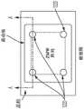
图7示出了图4A的顶盖和流动池被移除的核酸测序盒的前侧立体图。Fig. 7 shows a front perspective view of the nucleic acid sequencing cartridge with the top cover and flow cell of Fig. 4A removed.
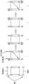
图8A和图8B示出了两个示例性四端口流动池的设计特征。图8C示出了示例性二端口流动池的俯视图。图8D示出了使用二端口流动池工艺(顶部)或传统的开放孔工艺(底部)加载的芯片的热力图的比较。图8E示出了使用四端口流动池加载芯片的示例性过程。8A and 8B illustrate design features of two exemplary four-port flow cells. Figure 8C shows a top view of an exemplary two-port flow cell. Figure 8D shows a comparison of thermograms for chips loaded using a two-port flow cell process (top) or a conventional open-pore process (bottom). Figure 8E shows an exemplary process for loading a chip using a four-port flow cell.
图9示出了用于使核酸测序盒的流动池与分析仪器接口连接的示例性流体夹持机构。9 illustrates an exemplary fluid clamping mechanism for interfacing a flow cell of a nucleic acid sequencing cartridge with an analytical instrument.
图10示出了用于核酸测序系统的示例性冷却系统。Figure 10 illustrates an exemplary cooling system for a nucleic acid sequencing system.
图11示出了包括插入的盒型核酸测序装置的用于核酸测序的示例性系统。FIG. 11 shows an exemplary system for nucleic acid sequencing including an inserted cassette nucleic acid sequencing device.
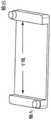
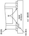
图12A和图12B示出了具有附接的流动池的复用光学芯片的两个视图。图12C-图12F示出了通过流动池的结构组件使激发光能量的通道最小化的新颖设计。12A and 12B show two views of a multiplexed optical chip with attached flow cells. Figures 12C-12F illustrate a novel design to minimize the passage of excitation light energy through the structural components of the flow cell.
图13A和图13B示出了利用光学芯片装置上的样本的流动、回流和再循环的样本加载工作流程。13A and 13B illustrate a sample loading workflow utilizing flow, reflow and recirculation of samples on an optical chip device.
图14示出了由用户将核酸样本输送到光学芯片装置上的示例性总体工作流程。Figure 14 illustrates an exemplary overall workflow for delivery of nucleic acid samples by a user onto an optical chip device.
图15示出了示例性的小体积样本输送装置。Figure 15 illustrates an exemplary small volume sample delivery device.
图16示出了可选的小体积样本输送装置。Figure 16 shows an alternative small volume sample delivery device.
图17A和图17B示出了具有相关联的样本储存器和流体阀的示例性盒式装置。17A and 17B illustrate an exemplary cartridge with associated sample reservoirs and fluid valves.
图18A-图18D提供了可选的盒式装置的实施例的流体管线体积的比较。18A-18D provide a comparison of fluid line volumes for alternative cassette device embodiments.
具体实施方式Detailed ways
概述overview
图1中示出了包括光源和集成目标波导装置的示例性光学分析系统。用作光源的激光器或激光系统110发射照明光115(也称为光激发信号或光激发束)到自由空间中。在该图中表示的激光器110在一些情况下可以直接发射光115到自由空间中。在其他情况下,激光器110包括其他光学元件,光在被发射到自由空间中之前行进通过这些光学元件。例如,在发射照明光115到自由空间中之前,包括其它光学元件的激光器可以包括光纤、PLC或两者的组合。在一些情况下,从激光器发射的照明光被直接发送到目标(例如目标装置170),该目标在本文中也可以称为“复用光学芯片”。通常,照明光115穿过用于在到达目标之前成形、操纵(导向)或以其它方式控制照明光的性质的一个或多个光学元件120。已经由一个或多个光学元件120成形和操纵的照明光117耦合到光波导140中。光通过光波导传送到目标装置上的关注区域150。通常,且如本文所示,使用例如光栅耦合器等光耦合器130发射照明光到光学波导中。虽然示出了光栅耦合器,但是应当理解,任何类型的耦合器、棱镜或其它接口光学元件或包括例如直接对接耦合等方法,都可以用于将光激发信号从光源引导到光波导中。An exemplary optical analysis system including a light source and an integrated target waveguide is shown in FIG. 1 . A laser or
就核酸测序装置来说,关注区域150也可以称为“测序区域”或者“测序范围”,关注区域具有多个反应区域155,例如纳米孔或零模式波导(ZMW)。光波导140通常在反应区域155下方延伸,从而通过与渐逝波照明进行光耦合以从下方照射反应区域。反应区域优选地包括荧光反应物,当被渐逝波照明激发时,荧光反应物发射可以被检测以便进行期望的分析(例如,核酸测序)的荧光190。在一些情况下,并且如这里所示,目标装置还具有集成传感器180(也称为光学检测器)。从反应区域发射的荧光通过该装置光耦合,以在光学检测器内的单个像素或像素组185处被检测。例如公开号为2008/0128627、2012/0085894、2016/0334334、2016/0363728、2016/0273034、2016/0061740和2017/0145498的美国专利申请中,描述了这种用于荧光分析的集成目标装置,上述各专利申请通过引用全部并入本文。包括集成光学检测器的目标装置通常还包括电子输出装置175。例如,集成光学检测器检测并处理光发射信号,然后通过一个或多个电子输出发送与检测到的信号相关的电子数据到装置之外。电子输出可以是例如硅芯片上的接合焊盘,接合焊盘通常被引线接合到芯片封装,并且芯片封装将具有用于传递来自芯片的电信号的电子输出。电信号通常被发送到计算机(未示出),该计算机处理接收到的信号以执行期望的分析。As far as the nucleic acid sequencing device is concerned, the region of
目标装置上的光波导可以是任何合适的波导,包括光纤、平面波导或通道波导。通常使用信道波导。波导优选地是单模波导,但是对于一些应用,波导可以是多模波导。The optical waveguides on the target device can be any suitable waveguides, including optical fibers, planar waveguides, or channel waveguides. Typically channel waveguides are used. The waveguide is preferably a single mode waveguide, but for some applications the waveguide may be a multimode waveguide.
在图1中,光波导140示出为形成在目标装置上,该目标装置可以是例如硅芯片等半导体芯片。本公开所关注的特定系统是SiON波导,例如形成在硅芯片上的那些波导。SiON波导将具有SiON芯,并且通常由较低折射率的例如二氧化硅(SiO2)等包层材料包围。如本领域所公知的,SiON可以在沉积工艺中形成,并且可以调节元素的比率以控制波导的光学特性。例如,可以改变氧气与氮气的比率以便改变膜的折射率。对于本公开的装置和系统的SiON波导,通常控制组合物以具有大于约1.6、大于约1.7或大于约1.8的折射率。例如,可以在钠D线(D光)上测量折射率。In FIG. 1 , an
波导寻址的分析装置和系统Analysis device and system for waveguide addressing
本公开总体上涉及用于执行分析操作,并且特别是用于化学、生物、医疗和其他研究和诊断应用中的化学、生物化学和生物反应的光学分析的改进的装置和系统。这些装置和系统特别适用于集成分析组件,例如,其中整个分析系统的多个功能组件共同集成在单个模块化组件内。然而,如在阅读以下公开内容时将清楚了解的,本公开的多个方面将具有除此类集成装置和系统之外的广泛效用。The present disclosure relates generally to improved devices and systems for performing analytical operations, and in particular for optical analysis of chemical, biochemical and biological reactions in chemical, biological, medical and other research and diagnostic applications. These devices and systems are particularly suitable for integrating analytical components, for example, where multiple functional components of an overall analytical system are co-integrated within a single modular component. However, as will be apparent upon reading the following disclosure, aspects of the present disclosure will have broad utility beyond such integrated devices and systems.
通常,作为本公开的主题的光学分析试图从关注的反应中收集和检测一个或多个光发射信号,该关注反应的出现或消失或其定位表示给定的化学或生物反应和/或给定物质在样本材料内存在或不存在。在一些情况下,反应物、反应物的产物或其它关注的物质(所有这些在此都称为反应物)固有地存在光学可检测信号。在其它情况下,反应物设置有外源标记基团以促进它们的检测。In general, optical analysis, which is the subject of this disclosure, attempts to collect and detect one or more light emission signals from reactions of interest, the presence or absence or location of which is indicative of a given chemical or biological reaction and/or a given The presence or absence of a substance within the sample material. In some cases, reactants, products of reactants, or other species of interest (all referred to herein as reactants) inherently present an optically detectable signal. In other cases, reactants are provided with exogenous labeling groups to facilitate their detection.
核酸测序nucleic acid sequencing
如本领域普通技术人员所理解的,荧光标记的核苷酸用于多种不同的核酸测序分析。例如,在一些情况下,此类标记用于监测引物延伸反应中聚合酶介导的、模板依赖性的核苷酸掺入。特别地,标记的核苷酸可以被引入引物模板聚合酶复合物,并且可以检测标记的核苷酸掺入检测到的引物中。如果特定类型的核苷酸掺入给定位置,则指示模板分子的序列中的潜在和互补核苷酸。在传统的桑格测序过程中,掺入的标记核苷酸的检测利用末端反应,其中标记的核苷酸携带阻断引物进一步延伸的末端基团。通过将标记的末端核苷酸与未标记的天然核苷酸混合,产生在不同核苷酸处末端的嵌套片段组。然后,这些片段可以通过毛细管电泳或其它合适的技术分离,以区分那些相差单个核苷酸的片段,并且可以以增加片段大小的顺序读取片段的标记,以提供片段的序列(如最后添加的、标记的末端核苷酸所示)。通过在添加的每种类型的核苷酸上提供不同的荧光标记,可以容易地区分序列中的不同核苷酸(参见,例如,专利号为5,821,058的美国专利,该专利通过引用全部并入本文以用于各个目的)。As understood by those of ordinary skill in the art, fluorescently labeled nucleotides are used in a variety of different nucleic acid sequencing analyses. For example, in some cases, such labels are used to monitor polymerase-mediated, template-dependent incorporation of nucleotides in primer extension reactions. In particular, labeled nucleotides can be introduced into a primer template polymerase complex, and incorporation of labeled nucleotides into detected primers can be detected. If a particular type of nucleotide is incorporated at a given position, it is indicative of potential and complementary nucleotides in the sequence of the template molecule. During traditional Sanger sequencing, the detection of incorporated labeled nucleotides utilizes end reactions, in which labeled nucleotides carry end groups that block further primer extension. Sets of nested fragments terminating at different nucleotides are generated by mixing labeled terminal nucleotides with unlabeled natural nucleotides. These fragments can then be separated by capillary electrophoresis or other suitable technique to distinguish those fragments that differ by a single nucleotide, and the fragment tags can be read in order of increasing fragment size to provide the sequence of the fragment (as last added , labeled terminal nucleotides). By providing a different fluorescent label on each type of nucleotide added, the different nucleotides in the sequence can be easily distinguished (see, e.g., U.S. Patent No. 5,821,058, which is incorporated herein by reference in its entirety) for various purposes).
在一些测序技术中,引物-模板复合物的阵列被固定在基板的表面上,使得单个分子或单个和同质分子组(克隆群体)分别与其他单个分子或分子组在空间上分离。以结果是单个核苷酸被添加到每个单独的分子或分子组的方式,标记的核苷酸被添加。在添加核苷酸之后,检测并鉴定标记的添加。In some sequencing technologies, arrays of primer-template complexes are immobilized on the surface of a substrate such that individual molecules or individual and homogeneous groups of molecules (clonal populations), respectively, are spatially separated from other individual molecules or groups of molecules. Labeled nucleotides are added in such a way that the result is that a single nucleotide is added to each individual molecule or group of molecules. Following the addition of nucleotides, the addition of the label is detected and identified.
在一些情况下,测序分析利用一次添加单一类型的核苷酸,随后是洗涤步骤。然后检测添加的标记核苷酸,除去核苷酸的标记,并用不同的核苷酸类型重复该过程。通过在基板上给定位置的标记的出现顺序来确定各个模板序列的序列。In some cases, sequencing analysis utilizes the addition of a single type of nucleotide at a time, followed by washing steps. Added labeled nucleotides are then detected, the label of the nucleotide is removed, and the process is repeated with a different nucleotide type. The sequence of each template sequence is determined by the order of occurrence of the markers at a given position on the substrate.
在其它类似的情况下,固定的复合物与所有四种类型的标记的核苷酸接触,其中每种类型的核苷酸携带可区分的荧光标记和末端基团,防止在给定步骤中添加多于一个的核苷酸。在单个掺入到每个单独的模板序列(或模板序列组)中之后,未结合的核苷酸被洗去,并且扫描固定的复合物以鉴定在每个位置添加了哪个核苷酸。重复该过程产生每个模板序列的序列信息。在其它情况下,使用超过四种类型的标记核苷酸。In otherwise similar cases, immobilized complexes are contacted with all four types of labeled nucleotides, where each type of nucleotide carries a distinguishable fluorescent label and an end group that prevents the addition of nucleotides at a given step. more than one nucleotide. After individual incorporation into each individual template sequence (or set of template sequences), unbound nucleotides are washed away, and the immobilized complex is scanned to identify which nucleotide was added at each position. This process is repeated to generate sequence information for each template sequence. In other cases, more than four types of labeled nucleotides are used.
在特别优选的方法中,在掺入过程本身期间,通过单个分子复合物实时检测标记的核苷酸。例如,在专利号为7,056,661的美国专利中描述了这样的方法,该专利通过引用全部并入本文以用于各个目的。在这些方法中,核苷酸被标记在掺入过程中释放的末端磷酸基团上,以避免标记积累在延伸产物上,并因此避免任何需要移除可能对复合物有害的标记的过程。在聚合过程中观察引物/模板聚合酶复合物,并通过其相关标记检测添加的核苷酸。In a particularly preferred method, the labeled nucleotides are detected in real time by single molecular complexes during the incorporation process itself. Such methods are described, for example, in US Patent No. 7,056,661, which is hereby incorporated by reference in its entirety for all purposes. In these methods, nucleotides are labeled on terminal phosphate groups released during incorporation to avoid label accumulation on extension products and thus avoid any process that would require removal of label that could be detrimental to the complex. The primer/template polymerase complex is observed during polymerization and the added nucleotides are detected by their associated labels.
在一个特定实例中,可使用限制激发辐射暴露于紧邻围绕个别引物/模板聚合酶复合物的体积的光学限制结构(例如零模式波导)来观察标记的核苷酸(参见例如专利号为6,917,726的美国专利,其通过引用的方式全部并入本文中以用于各个目的)。因此,只有在被掺入的过程中被聚合酶保留的标记的核苷酸暴露于激发照明一段时间,该时间足以产生荧光并因此鉴定掺入的核苷酸。具有纳米级孔阵列或零模式波导阵列的示例性芯片因此被认为适合于这些目的,该示例性芯片包括在硅胶基层上具有金属或金属氧化物层的基板,其中纳米级孔设置成穿过金属或金属氧化物层到达或进入硅胶基层(参见例如专利号为6,917,726、7,302,146、7,907,800、8,802,600、8,906,670、8,993,307、8,994,946、9,223,084、9,372,308和9,624,540的美国专利,这些专利通过引用全部并入本文)。In a specific example, labeled nucleotides can be visualized using optical confinement structures (e.g., zero-mode waveguides) that limit excitation radiation exposure to the volume immediately surrounding the individual primer/template polymerase complexes (see, e.g., Patent No. 6,917,726 U.S. Patents, which are incorporated herein by reference in their entirety for all purposes). Thus, only labeled nucleotides that are retained by the polymerase during incorporation are exposed to excitation illumination for a period of time sufficient to generate fluorescence and thus identify the incorporated nucleotides. An exemplary chip having an array of nanoscale holes or an array of zero-mode waveguides is thus considered suitable for these purposes, the exemplary chip comprising a substrate having a layer of metal or metal oxide on a base layer of silica gel, wherein the nanoscale holes are disposed through the metal or the metal oxide layer to or into the silica gel-based layer (see, e.g., U.S. Patent Nos. 6,917,726, 7,302,146, 7,907,800, 8,802,600, 8,906,670, 8,993,307, 8,994,946, 9,223,084, 9,372,308, and 9,624,540, which are incorporated herein by reference in their entirety).
在另一种方法中,核苷酸上的标记配置成与复合物上或附近的互补基团相互作用(例如附着在聚合酶上),其中相互作用提供独特的信号。例如,聚合酶可设置有在第一波长激发并在第二波长发射的供体荧光团,而待添加的核苷酸用在第二波长激发但在第三波长发射的荧光团标记(参见,例如,先前并入本文的专利号为7,056,661的美国专利)。结果,当核苷酸和聚合酶彼此足够接近以允许能量从供体荧光团转移到核苷酸上的标记时,产生独特的信号。同样,在这些情况下,各种类型的核苷酸设置有独特的荧光标记,该标记允许通过标记的光谱鉴定或其他光学标签来识别核苷酸。In another approach, a label on the nucleotide is configured to interact with a complementary group on or near the complex (eg, attached to a polymerase), where the interaction provides a unique signal. For example, a polymerase can be provided with a donor fluorophore excited at a first wavelength and emitted at a second wavelength, while the nucleotide to be added is labeled with a fluorophore excited at the second wavelength but emitted at a third wavelength (see, For example, US Patent No. 7,056,661, previously incorporated herein). As a result, a unique signal is generated when the nucleotide and polymerase are in close enough proximity to each other to allow energy transfer from the donor fluorophore to the label on the nucleotide. Also, in these cases, various types of nucleotides are provided with unique fluorescent labels that allow identification of the nucleotides by spectral identification of the labels or other optical tags.
在上述各种示例性过程中,检测到来自反应区域的信号事件指示反应已经发生。此外,对于许多上述方法,通过区分信号事件的光谱特征,也可以实现反应性质的鉴定,例如,在给定时间在引物延伸反应中添加了哪个核苷酸,或者哪个核苷酸与模板分子中的给定位置互补。In various exemplary processes described above, detection of a signal event from the reaction zone indicates that a reaction has occurred. In addition, for many of the methods described above, by distinguishing the spectral signature of the signaling event, identification of the nature of the reaction, for example, which nucleotide was added at a given time in a primer extension reaction, or which nucleotide interacted with the template molecule The given positions are complementary.
本公开的分析系统的光路起到一个或多个将激发辐射输送到反应区域的作用,例如,以激发荧光标记的分子,然后该荧光标记的分子发射相关的光发射信号,以传送从反应区域发射的光信号到光学检测器,并且对于多光谱信号,即,可以通过荧光标记的分子发射光谱区分的多个信号,分离那些信号,使得那些信号可以被区别性地检测,例如,通过将不同的信号引导至不同的光学检测器或相同光学检测器阵列上的不同区域。然后将区别性检测的信号与反应的发生(例如在给定位置添加核苷酸)和反应性质的测定(例如添加的核苷酸被鉴定为特定核苷酸类型,例如腺苷)两者相关联。The optical path of the assay system of the present disclosure serves one or more roles in delivering excitation radiation to the reaction region, for example, to excite a fluorescently labeled molecule, which then emits an associated light emission signal for delivery from the reaction region. The emitted light signal is to an optical detector, and for multispectral signals, that is, multiple signals that can be distinguished by the emission spectra of fluorescently labeled molecules, separating those signals so that those signals can be detected differentially, for example, by combining different Signals from the array are directed to different optical detectors or to different regions on the same optical detector array. The differentially detected signal is then correlated with both the occurrence of the reaction (e.g. addition of a nucleotide at a given position) and the determination of the nature of the reaction (e.g. the added nucleotide is identified as a specific nucleotide type, e.g. adenosine) couplet.
在用于核酸测序的常规的、空间完全自由的分析系统中,优选地,用于将激发光输送至反应区域和从反应区域传送光学信号至检测器的光学系统可以使整个系统尺寸、复杂性和成本这些方面被降低。例如,这样的光学系统可以包括透镜、色散元件、分束器、扩束器、准直器、空间和光谱滤光器和二向色镜的集合,这些组件全部被装配以输送目标化的和均匀的照明分布到不同的反应区域。在大规模系统中,这些组件必须被制造、组装和调整以确保适当的对准、聚焦和与其他光和振动源的隔离,以优化激发光到反应区域的传送。随着寻址反应区域的数量或系统对激发光强度的变化的灵敏度增加,解决这些问题和其它问题变得更加重要,并且同样通常涉及包括附加组件的光学系统,例如对准和聚焦机构、隔离结构等。In a conventional, completely spatially free analysis system for nucleic acid sequencing, preferably the optical system for delivering the excitation light to the reaction area and the optical signal from the reaction area to the detector can make the overall system size, complexity and costs in these areas are reduced. For example, such an optical system may include a collection of lenses, dispersive elements, beam splitters, beam expanders, collimators, spatial and spectral filters, and dichroic mirrors, all assembled to deliver targeted and Uniform lighting distribution to the different reaction areas. In large-scale systems, these components must be fabricated, assembled, and tuned to ensure proper alignment, focusing, and isolation from other sources of light and vibration to optimize the delivery of excitation light to the reaction region. Addressing these and other issues becomes more important as the number of addressed reaction regions or the sensitivity of the system to changes in excitation light intensity increases, and again often involves optical systems that include additional components, such as alignment and focusing mechanisms, isolation structure etc.
关于光发射信号的收集和检测,常规系统通常采用从反应区域收集光发射信号的光学系统,例如,通过物镜系统,通过一个或多个滤波级传送各种不同的信号,该滤波级通常由一个或多个分色镜构成,分色镜有差别地传送和反射不同波长的光,以便引导光谱上不同的光信号到不同检测器或给定检测器上的区域。然后检测这些分离的光学信号,并用来鉴定产生这种信号的反应的性质。如将了解的,这些区分方向的光学装置的使用以多个检测器、多个透镜及滤光器系统的形式对整个系统给出相当大的空间、尺寸及成本要求,且在许多情况下产生复杂的对准及相关问题。当光学系统与激发照明共享一个或多个子路径时,许多这种困难进一步加重,因为信号处理将包括从每个检测信号中分离出背景激发照明的进一步要求。With regard to the collection and detection of light emission signals, conventional systems typically employ an optical system that collects light emission signals from the reaction region, for example, through an objective lens system, passing the various signals through one or more filtering stages, usually composed of a One or more dichroic mirrors that differentially transmit and reflect light of different wavelengths to direct spectrally different light signals to different detectors or regions on a given detector. These separated optical signals are then detected and used to characterize the nature of the reaction that produced the signal. As will be appreciated, the use of these direction-discriminating optics places considerable space, size and cost requirements on the overall system in the form of multiple detectors, multiple lenses and filter systems, and in many cases creates Complex alignment and related issues. Many of these difficulties are further exacerbated when the optical system shares one or more subpaths with the excitation illumination, as signal processing will include the further requirement of separating the background excitation illumination from each detection signal.
同样,如同上述激发光学系统,随着系统的灵敏度和复用增加,这增加了在这些系统中必须解决的问题,增加了已经很复杂的光学系统的复杂性。此外,光学系统中的光学元件的数量越多,将不必要的扰动引入该系统的风险以及由此产生的信号检测能力越大。例如,光学元件中的光学像差在信号检测中产生额外的困难,光学元件也会产生额外的困难,这些光学元件可能将某种水平的自发荧光注入到光学系统中,然后必须将其与信号事件区分开。Also, as with the excitation optics described above, as the sensitivity and multiplexing of the systems increase, this increases the problems that must be solved in these systems, adding to the complexity of an already complex optical system. Furthermore, the greater the number of optical elements in an optical system, the greater the risk of introducing unwanted perturbations into the system and thus the signal detection capability. For example, optical aberrations in the optics create additional difficulties in signal detection, as can optics that may inject some level of autofluorescence into the optics, which must then be compared to the signal Events are separated.
在一些实施例中,本公开的系统还包括计算机,该计算机从光学检测器或光学检测器的区域接收至少一个电信号,例如上文所述的检测信号,并且分析所述至少一个电信号。更具体地说,如本领域普通技术人员所理解的,由计算机进行的分析可以包括从电信号获得核酸测序信息。In some embodiments, the system of the present disclosure also includes a computer that receives at least one electrical signal from the optical detector or a region of the optical detector, such as the detection signal described above, and analyzes the at least one electrical signal. More specifically, analysis by computer may include obtaining nucleic acid sequencing information from electrical signals, as understood by those of ordinary skill in the art.
集成装置Integrated device
本公开的核酸测序盒、封装装置和分析系统通常包括一个或多个小规模集成分析装置,可选地还包括一个或多个反应区域、流体组分和激发照明路径以及可选激发的照明源。将上述组件中的一些或全部集成到单个小型化分析装置(也称为复用光学芯片)中解决了较大的非集成分析系统所面临的许多问题,例如尺寸、成本、重量、与长路径或自由空间光学相关联的低效率等。例如,公开号为2008/0128627、2012/0085894、2016/0334334、2016/0363728、2016/0273034、2016/0061740和2017/0145498的美国专利申请中描述了包括用于照射纳米级样本的集成波导的高度复用分析系统,这些专利申请通过引用全部并入本文。用于高度复用分析的其它纳米级照明系统在公开号为2014/0199016和2014/0287964的美国专利申请中有所描述,各申请通过引用全部并入本文。The nucleic acid sequencing cartridges, packaged devices and analysis systems of the present disclosure generally include one or more small-scale integrated analysis devices, optionally also including one or more reaction regions, fluid components and excitation illumination paths and optional excitation illumination sources . Integrating some or all of the above components into a single miniaturized analysis device (also known as a multiplexed optical chip) solves many of the problems faced by larger non-integrated analysis systems, such as size, cost, weight, and long paths Or the inefficiencies associated with free-space optics, etc. For example, U.S. Patent Application Publication Nos. 2008/0128627, 2012/0085894, 2016/0334334, 2016/0363728, 2016/0273034, 2016/0061740, and 2017/0145498 describe devices that include integrated waveguides for illuminating nanoscale samples. Highly Multiplexed Assay Systems, these patent applications are hereby incorporated by reference in their entirety. Other nanoscale illumination systems for highly multiplexed analysis are described in US Patent Application Publication Nos. 2014/0199016 and 2014/0287964, each of which is incorporated herein by reference in its entirety.
这种集成分析系统的其它例子在例如公开号为2012/0014837、2012/0019828和2012/0021525的美国专利申请中有所描述,这些专利申请通过引用全部并入本文。通过将检测元件与反应区域直接或作为耦合组件集成,可以消除对自由空间光学系统所需的许多不同组件(例如多个传送光学装置、透镜、反射镜等)的需要。在许多情况下,也可以消除其它光学组件,例如各种对准功能,因为通过检测元件与反应区域的直接集成能实现对准。本公开的盒、封装装置和系统通过在更大程度上简化分析装置的光学、电子、流体、机械和热组件,进一步改善了由这种复用装置提供的益处,从而进一步降低了这种装置的成本和复杂性,并且进一步改善了该过程中的可用信号。Other examples of such integrated analysis systems are described, for example, in US Patent Application Publication Nos. 2012/0014837, 2012/0019828, and 2012/0021525, which are hereby incorporated by reference in their entirety. By integrating the detection element with the reaction region directly or as a coupling component, the need for many of the different components required for free-space optical systems (eg, multiple delivery optics, lenses, mirrors, etc.) can be eliminated. In many cases, other optical components, such as various alignment functions, can also be eliminated, since the alignment is achieved by the direct integration of the detection element with the reaction area. The cartridges, packaged devices, and systems of the present disclosure further improve the benefits provided by such multiplexed devices by simplifying the optical, electronic, fluidic, mechanical and thermal components of the analytical device to a greater extent, thereby further reducing the cost of such devices. cost and complexity, and further improves the available signals in the process.
在示例性实施例中,本公开的盒、封装装置和系统的复用光学芯片包括形成为单个集成装置的分析装置的阵列,该单个集成装置通常配置成作为可消耗装置单次使用。在各种实施例中,集成装置包括其它组件,包括但不限于本地流体、电子连接器、电源、照明元件、检测器、逻辑和处理电路。如上所述,阵列中的每个分析装置优选地配置成用于执行分析操作。In exemplary embodiments, the multiplexed optical chips of the cartridges, packaged devices, and systems of the present disclosure include an array of analytical devices formed as a single integrated device, typically configured for a single use as a consumable device. In various embodiments, the integrated device includes other components including, but not limited to, local fluids, electrical connectors, power supplies, lighting elements, detectors, logic and processing circuits. As noted above, each analysis device in the array is preferably configured to perform an analysis operation.
虽然系统中的每个集成装置的组件和装置的配置可以变化,但是系统内的每个分析装置可以至少部分地包括如图2中的框图所示的一般结构。如图所示,分析装置200通常包括反应池202,在反应池中设置反应物,并从反应池发出光发射信号。“反应池”应理解为通常用于分析和化学领域,是指发生关注的反应的位置。因此,“反应池”可以包括完全独立的反应孔、容器、流动池、室等,例如由一个或多个结构屏障、壁、盖等封闭的,或者反应池可以包括在基板上和/或在给定的反应孔、容器、流动池等内的特定区域,例如在相邻的反应池之间没有结构限制或抑制。反应池可以包括结构元件以增强反应或其分析,例如光学限制结构、纳米孔、柱、表面处理,例如疏水或亲水区域、结合区域等。While the components of each integrated device in the system and the configuration of the device may vary, each analysis device within the system may at least partially include the general structure shown in the block diagram in FIG. 2 . As shown, the
在各个方面,“分析装置”或“集成分析装置”是指功能性连接的反应池和相关组件。在各个方面,“分析系统”是指包括分析装置和用于执行分析操作的其它仪器的较大系统。例如,在一些情况下,本公开的核酸测序盒和封装装置是分析仪器或分析系统的一部分。核酸测序盒或封装装置可以可移除地耦合到仪器中。在测序盒或封装装置与系统连接之前或之后,可以使液体样本和/或试剂与测序盒或封装装置接触。该系统可以向测序盒或封装装置提供电信号和/或照明光,并且可以从测序盒或封装装置中的检测器或其他电子组件接收电信号。该系统还可以提供对测序盒或封装装置的机械支撑和/或与测序盒或封装装置的热交换。该仪器或系统可以具有计算机,以操作、存储和分析来自测序盒或封装装置的数据。例如,该仪器可以具有在核酸测序反应中鉴定添加的核苷酸类似物的顺序的能力。例如,可以如专利号为8,182,993的美国专利中所描述的进行识别,该专利通过引用并入本文。In various aspects, "analytical device" or "integrated analytical device" refers to functionally linked reaction cells and related components. In various aspects, "analytical system" refers to a larger system that includes analytical devices and other instrumentation for performing analytical operations. For example, in some cases, the nucleic acid sequencing cartridges and packaged devices of the present disclosure are part of an analytical instrument or analytical system. A nucleic acid sequencing cartridge or packaging device can be removably coupled to an instrument. Liquid samples and/or reagents can be brought into contact with the sequencing cartridge or packaging device either before or after connection of the sequencing cartridge or packaging device to the system. The system can provide electrical signals and/or illumination light to the sequencing cartridge or packaging device, and can receive electrical signals from detectors or other electronic components in the sequencing cartridge or packaging device. The system can also provide mechanical support for and/or heat exchange with the sequencing cartridge or packaging device. The instrument or system may have a computer to manipulate, store and analyze data from the sequencing cartridge or packaged device. For example, the instrument may have the capability to identify the sequence of added nucleotide analogs in a nucleic acid sequencing reaction. For example, identification can be performed as described in US Patent No. 8,182,993, which is incorporated herein by reference.
在一些情况下,一种或多种涉及关注的反应物可以被固定、夹带或以其他方式定位在给定的反应池内。有多种技术可用于定位和/或固定反应物,包括通过共价或非共价连接的表面固定、基于珠或颗粒的固定,随后定位珠或颗粒、在给定位置处的基质中夹带等。反应池可以包括分子的集合体,例如溶液或分子块,或者它们可以包括单独的分子反应复合物,例如,作为复合物参与关注的反应的每个微粒的一个分子。类似地,本公开的测序盒和封装装置可以包括单独的反应池,或者可以包括集成结构(例如多壁或多池板、芯片、基板或系统)中的反应池的集合、阵列或其它分组。此类排列的反应池的一些实例包括核酸阵列芯片,例如

尽管分析系统可以包括具有单一波导层和反应池层的分析装置阵列,但是可以理解,在仍然实现装置的目标的同时,可以在波导阵列基板和包层/反应池层中采用各种层组合物(参见,例如,专利号为7,820,983的美国专利,通过引用并入本文以用于各个目的)。Although an analytical system may include an array of analytical devices having a single waveguide layer and reaction cell layer, it is understood that various layer compositions may be employed in the waveguide array substrate and cladding/reaction cell layer while still achieving the goals of the device (See, eg, US Patent No. 7,820,983, incorporated herein by reference for all purposes).
本公开的盒、封装装置和系统的复用光学芯片通常包括如图2所示的多个分析装置200,该装置具有设置成与反应池202光学连通的检测器元件220。反应池202和检测器元件220之间的光通信可以由光学系统204提供,该光学系统包括一个或多个光学元件206、208、210和212,用于有效地从反应池202引导信号到检测器220。这些光学元件通常可以包括任何数量的例如透镜、滤光器、光栅、反射镜、棱镜、折射材料等元件,或者这些元件的各种组合,这取决于应用的具体情况。除了用于从反应区域引导光发射信号到检测器的组件之外,芯片还可以具有用于传递照明光到反应区域以执行荧光测量的光学组件。The multiplexed optical chip of the cartridges, packaged devices, and systems of the present disclosure generally includes a plurality of
在各种实施例中,反应池202和检测器元件220与一个或多个光学元件一起被设置在集成装置结构中。通过将这些元件集成到单个装置结构中,可以提高反应池和检测器之间的光耦合效率。如本文所使用的,当涉及分析装置的不同组件时,术语“集成”通常是指彼此耦合以便相对于彼此固定的两个或更多个组件。这样,集成的组件可以不可逆地或永久地集成,这意味着分离将损坏或破坏一个或两个元件,或者这些组件可以可移除地集成,其中一个组件可以从另一个组件分离,只要当组件集成时,它们相对于彼此保持基本上不动。在一些情况下,这些组件集成在一起,例如作为单个制造的装置,诸如在单个硅芯片中。在一些情况下,检测器组件是单独仪器的一部分,并且反应池组件是可拆卸装置(例如可拆卸芯片)的一部分。在芯片中的反应池组件在与检测器组件分离的情况下,用于从反应池引导光发射信号到检测器的光学元件组件可以在反应池组件中、在检测器组件中、或者在其中一些组件在反应池组件中而其它组件在检测器组件中的组合中。In various embodiments, reaction well 202 and
在常规的光学分析系统中,通常放置分立的反应容器在光学仪器中,该光学仪器仅利用自由空间光学器件来传送光学信号到反应容器和从反应容器传送光学信号到检测器。这些自由空间光学器件往往包括较高质量和体积的组件,并且具有导致这种系统具有许多弱点的自由空间界面。例如,由于从这些较高质量组件引入了不希望的泄漏路径,这种系统具有较大的光损失倾向。这些高质量组件通常还引入更高水平的自发荧光。所有这些固有的弱点都降低了系统的信噪比(SNR),并降低了其总灵敏度,这又可能影响系统的速度、精度和吞吐量。另外,在复用应用中,来自多个反应区域(即,多个反应池,或单个池内的多个反应位置)的信号通常通过公共光学系统或光学系统的公共部分,使用该系统中的光学元件的全部体积以成像到检测器平面上。结果,在这些光学组件中存在的光学像差,(例如衍射、散射、像散和彗差)使信号在振幅和视场上都劣化,导致更大的噪声影响和检测信号之间的串扰。In conventional optical analysis systems, discrete reaction vessels are typically placed in an optical instrument that utilizes only free-space optics to transmit optical signals to and from the reaction vessel to the detector. These free-space optics tend to include relatively high mass and bulky components, and have free-space interfaces that lead to many weaknesses of such systems. For example, such systems have a greater propensity for light loss due to the introduction of unwanted leakage paths from these higher quality components. These high-quality components often also introduce higher levels of autofluorescence. All of these inherent weaknesses reduce the system's signal-to-noise ratio (SNR) and reduce its overall sensitivity, which in turn can affect the system's speed, accuracy, and throughput. Additionally, in multiplexing applications, signals from multiple reaction zones (i.e., multiple reaction cells, or multiple reaction positions within a single cell) typically pass through a common optical system or common portion of an optical system using the optical The entire volume of the element is imaged onto the detector plane. As a result, optical aberrations present in these optical components, such as diffraction, scatter, astigmatism, and coma, degrade the signal both in amplitude and field of view, leading to greater noise effects and crosstalk between detected signals.
在一些情况下,本公开的复用光学芯片的反应区域包括纳米级孔,例如,该纳米级孔具有不大于500nm的线性尺寸。本公开的光学芯片的纳米级孔可以例如是具有在约50nm和200nm之间的底部直径的圆柱形。孔的深度可以例如从大约50nm到大约400nm。在一些情况下,反应区域可以包括零模式波导(ZMW)。例如,在专利号为7,170,050、7,486,865和8,501,406的美国专利中描述了零模式波导,这些专利通过引用全部并入本文。In some cases, the reaction region of a multiplexed optical chip of the present disclosure includes a nanoscale well, for example, the nanoscale well has a linear dimension no greater than 500 nm. The nanoscale wells of the optical chips of the present disclosure may, for example, be cylindrical with a base diameter between about 50 nm and 200 nm. The depth of the pores may, for example, be from about 50 nm to about 400 nm. In some cases, the reactive region can include a zero-mode waveguide (ZMW). For example, zero-mode waveguides are described in US Patent Nos. 7,170,050, 7,486,865, and 8,501,406, which are hereby incorporated by reference in their entirety.
这种装置利用在其中发生信号反应的反应区域或容器与检测那些信号的检测器或检测器元件的接近度,以便利用该接近度呈现的益处。如上所述,这些益处包括光学系统的尺寸、重量和复杂性的减小,并且因此增加了系统的潜在复用,例如,可以在单个盒、封装装置或系统中集成和检测的不同反应区域的数量。另外,与在信号收集和检测中利用大的自由空间光学装置和多个相机的系统相比,这种接近度潜在地提供了在信号传送期间减少损失、减少来自相邻反应区域的信号串扰以及减少利用这种集成装置的整个系统的成本的益处。Such devices take advantage of the proximity of reaction regions or vessels in which signal reactions occur to detectors or detector elements that detect those signals in order to take advantage of the benefits presented by that proximity. As mentioned above, these benefits include a reduction in the size, weight, and complexity of the optical system, and thus increased potential multiplexing of the system, for example, the combination of different reaction regions that can be integrated and detected in a single cartridge, packaged device, or system. quantity. In addition, this proximity potentially provides for reduced losses during signal transfer, reduced signal crosstalk from adjacent reaction regions, and The benefit of reducing the cost of the overall system utilizing such an integrated device.
在本公开的复用光学芯片中,存在可以受益于优化的多个设计标准。例如,在这些光学芯片中,首要的目标是使介入光学元件最小化,所述介入光学元件可能干扰光发射信号从反应区域到检测器的有效传送,以及通过增加反应区域和传感器之间的光学元件的复杂性而导致成本和对装置的空间需求的增加。In the multiplexed optical chips of the present disclosure, there are a number of design criteria that can benefit from optimization. For example, in these optical chips, the primary goal is to minimize intervening optical elements that may interfere with the efficient transfer of the light emission signal from the reaction area to the detector, and by increasing the optical density between the reaction area and the sensor. The complexity of the components leads to an increase in cost and space requirements for the device.
另外,并且对于单分子检测系统而言更重要的是,对于任何给定反应事件,最大化所检测的光发射信号的量也是重要的。特别地,在单个分子事件的光学检测中,在测量中通常依赖于与关注事件相对应的相对少量的光子。虽然例如荧光染料等高量子产率标记基团可以提高可检测性,但是这样的系统仍然在光学系统的检测能力的较低端操作。在使用本系统进行的分析反应中发现效用的荧光染料是公知的。可以使用任何合适的,例如,如公开号为WO2013/173844A1的PCT国际申请和公开号为2009/0208957A1、2010/0255488A1、2012/0052506A1、2012/0058469A1、2012/0058473A1、2012/0058482A1和2012/0077189A1的美国专利申请中所述的荧光染料。Additionally, and more importantly for single molecule detection systems, it is also important to maximize the amount of light emission signal detected for any given reaction event. In particular, in the optical detection of single molecular events, a relatively small number of photons corresponding to the event of interest is often relied upon in the measurement. While high quantum yield labeling groups such as fluorescent dyes can improve detectability, such systems still operate at the lower end of the detection capabilities of the optical system. Fluorescent dyes that find utility in assay reactions performed using the present system are well known. Any suitable one may be used, for example, such as PCT International Application Publication No. WO2013/173844A1 and Publication Nos. Fluorescent dyes described in the U.S. patent application.
在本公开的盒、封装装置和系统的背景下,因为实现激发与信号分离的目标或实现一个信号与下一个信号分离的目标的可用空间较少,所以光路的尺寸和复杂性造成更大的困难。因此,本公开的盒、封装装置和系统的复用光学芯片利用与正在进行的分析相关的简化了的光路,以便优化针对那些光学芯片集成性质的分析。In the context of the cartridges, packaged devices, and systems of the present disclosure, the size and complexity of the optical path poses a greater difficulty. Thus, the multiplexed optical chips of the cartridges, packaged devices, and systems of the present disclosure utilize a simplified optical path associated with ongoing assays in order to optimize assays for the integrated nature of those optical chips.
图3更详细地示出了用于执行光学分析的装置结构的示例,所述光学分析例如核酸测序过程或单分子结合测定。如图所示,集成装置300包括在第一基板层304上限定的反应区域302。如图所示,反应区域302包括设置在基板表面中的孔。这种孔可以构成基板底面中的凹陷或穿过附加基板层设置到下面的透明基板的孔,例如,如在零模式波导阵列中使用的(参见,例如,专利号为7,181,122和7,907,800的美国专利)。图3示出了具有一个反应区域302的装置的一部分。通常,装置将具有多个反应区域,例如装置可以包括具有数千、至数百万、至数千万或甚至更多的单独反应区域的阵列。Figure 3 shows in more detail an example of a device structure for performing an optical analysis, such as a nucleic acid sequencing process or a single molecule binding assay. As shown, the
从激发光源(未示出)将激发照明输送到反应区域,该激发光源可以与光学装置分离或者可以集成到光学装置中。如图所示,光波导(或波导层)306用于将激发光(箭头所示)传送到反应区域302附近,其中从波导306发出的渐逝场照亮反应区域302内的反应物。使用光波导照射反应区域在例如专利号为7,820,983、8,207,509和8,274,040的美国专利中有所描述,这些专利通过引用并入本文。Excitation illumination is delivered to the reaction region from an excitation light source (not shown), which may be separate from the optics or may be integrated into the optics. As shown, an optical waveguide (or waveguide layer) 306 is used to transmit excitation light (shown by the arrow) near the
可选地,集成装置300包括光通道组件308,以有效地从反应区域引导发射光至设置在反应区域下方的检测器层312。检测器层通常包括多个检测器元件,例如,与给定反应区域302光耦合的四个所示检测器元件312a-d。对于DNA测序应用,经常需要实时监测四种不同的信号,每种信号对应于一种核酸碱基。不同的信号可以是可区分的,例如,通过波长、强度或任何其他合适的区别或区别的组合来区分。虽然图中示出为像素312a-d的线性布置,但是将意识到,可以以网格、n乘n正方形、环形阵列或任何其它方便的取向或布置来布置探测器元件。在一些情况下,每个检测器元件或通道将具有每个反应区域的单个像素,其中不同的分析信号可通过例如它们的不同强度来区分。在一些情况下,各检测器元件包括多个像素,例如每个反应区域两个、三个、四个或甚至更多个像素。检测器元件与延伸到芯片之外的导体电连接,用于向检测器元件提供电信号,并用于从检测器元件发送信号到例如所连接的处理器。在一些实施例中,检测器层是CMOS晶片等,即,由CMOS传感器或CCD阵列构成的晶片。例如,参见《CMOS成像器从光传导到图像处理(2004)》,Yadid-Pecht和Etienne-Cummings,eds.;《Springer》期刊;《CMOS/CCD传感器和照相机系统(2007)》,Holst和Lomheim;SPIE出版社。Optionally, the
然后检测并记录从反应区域302发射的、撞击在这些检测器元件上的信号。如图3的集成装置中所示,该装置可以另外包括在每个检测器元件上方的滤色器,例如,如设置在过滤层310中。如图所示,“过滤器a”对应于与“通道a”相关联的滤色器,“过滤器b”对应于与“通道b”相关联的滤色器等等。选择过滤器组以允许捕获光子的高产率,例如其中每个滤色器具有一个或多个阻断信号的阻断带,该阻断带阻断来自反应区域302中发生的反应发射的一个或多个光谱不同的信号的一部分的信号。具体地,过滤器设计成允许大部分发射光子通过,同时仍然区分四个碱基。当发射的信号通过它们的强度被区分时,单个检测器元件能够通过在一个波长或波长范围下由样本从反应区域发射的光强度的差异来识别多个信号,例如由多个不同的核酸碱基发射的信号。The signals emitted from the
在一些情况下,提供光学元件以选择性地引导来自给定波长组的光到给定检测器元件。通常,不使用特定的光重新定向,使得到达过滤层的每个区域的光基本上相同。In some cases, optical elements are provided to selectively direct light from a given set of wavelengths to a given detector element. Typically, no specific light redirection is used such that the light reaching each area of the filter layer is substantially the same.
检测器层可操作地与通常集成到基板中的适当电路耦合,以便向处理器提供信号响应,所述处理器可选地集成在同一装置结构内或者与检测器层和相关联电路分离但与检测器层和相关联电路电耦合。使用在此类装置中的电路类型的实例在先前以引用的方式并入本文中的公开号为2012/0019828的美国专利申请中有所描述。The detector layer is operatively coupled with appropriate circuitry, typically integrated into the substrate, to provide a signal response to a processor, which is optionally integrated within the same device structure or separate from the detector layer and associated circuitry but separate from the detector layer and associated circuitry. The detector layer and associated circuitry are electrically coupled. Examples of the types of circuitry used in such devices are described in US Patent Application Publication No. 2012/0019828, previously incorporated herein by reference.
本公开的复用光学芯片在本文中也可称为目标波导装置、目标装置或集成分析装置,其通常具有至少一个光耦合器和与光耦合器光耦合并将输入光信号输送到多个反应区域的集成波导。在一些实施例中,本公开的装置的光耦合器是低数值孔径耦合器。在一些实施例中,光耦合器是衍射光栅耦合器。在特定实施例中,光耦合器是具有低数值孔径的衍射光栅耦合器。在一些情况下,光源被引导到单个耦合器上,而在其他情况下,光源被引导到多个耦合器(例如从2个到16个耦合器)上。在一些情况下,每个耦合器接收基本上相同的功率。在某些情况下,不同的功率水平被引导到目标装置上的不同耦合器。虽然本说明书可能提到上述“耦合器”,但应当理解,在一些情况下可以存在单个耦合器,并且在其他情况下,在给定装置上存在多个耦合器。具有合适耦合器的目标波导装置例如在公开号为2016/0363728的美国专利申请中有所描述,该专利申请通过引用全部并入本文。The multiplexed optical chip of the present disclosure may also be referred to herein as a target waveguide device, a target device, or an integrated analysis device, which generally has at least one optical coupler and optically couples with the optical coupler and delivers the input optical signal to multiple reaction channels. area of integrated waveguides. In some embodiments, the optical couplers of the devices of the present disclosure are low numerical aperture couplers. In some embodiments, the optical coupler is a diffraction grating coupler. In a particular embodiment, the optical coupler is a diffraction grating coupler with a low numerical aperture. In some cases, the light source is directed onto a single coupler, while in other cases, the light source is directed onto multiple couplers (eg, from 2 to 16 couplers). In some cases, each coupler receives substantially the same power. In some cases, different power levels are directed to different couplers on the target device. While this specification may refer to "couplers" as described above, it should be understood that in some cases there may be a single coupler, and in other cases there may be multiple couplers on a given device. A target waveguide arrangement with a suitable coupler is described, for example, in US Patent Application Publication No. 2016/0363728, which is incorporated herein by reference in its entirety.
光栅耦合器及其将光耦合(通常来自光纤的光)到波导装置中的应用是本领域已知的。例如,专利号为3,674,335的美国专利公开了适于将光路由到薄膜波导中的反射和透射光栅耦合器。另外,专利号为7,245,803的美国专利公开了包括多个细长散射元件的改进的光栅耦合器。耦合器优选地具有带有窄端和宽端的扩口结构。该结构被认为在将光信号耦合进和耦合出平面波导结构方面提供了增强的效率。专利号为7,194,166的美国专利公开了适合于使波分复用光耦合到单模和多模光纤以及从单模和多模光纤耦合波分复用光的波导光栅耦合器。公开的装置包括安置在表面上的一组波导光栅耦合器,该波导光栅耦合器全部由来自光纤的光点照射。该组耦合器内的至少一个光栅耦合器被调谐到光束中的每个信道,并且因此该组耦合器对在光纤中传播的信道进行解复用。光栅耦合器的另外的示例在专利号为7,792,402的美国专利和公开号为WO2011/126718和WO2013/037900的PCT国际专利申请中公开。在专利号为7,058,261的美国专利中公开了使棱镜耦合和光栅耦合组合到集成波导装置中。在本公开的盒、封装装置和系统的复用光学芯片中,光能可由光纤、透镜、棱镜、反射镜或任何其它合适的光源提供。Grating couplers and their use to couple light, typically from optical fibers, into waveguides are known in the art. For example, US Patent No. 3,674,335 discloses reflective and transmissive grating couplers suitable for routing light into thin film waveguides. Additionally, US Patent No. 7,245,803 discloses an improved grating coupler comprising a plurality of elongated scattering elements. The coupler preferably has a flared configuration with a narrow end and a wide end. This structure is believed to provide enhanced efficiency in coupling optical signals into and out of the planar waveguide structure. US Patent No. 7,194,166 discloses a waveguide grating coupler suitable for coupling wavelength division multiplexed light to and from single mode and multimode fibers. The disclosed device includes a set of waveguide grating couplers disposed on a surface, all of which are illuminated by a spot of light from an optical fiber. At least one grating coupler within the set of couplers is tuned to each channel in the beam, and thus the set of couplers demultiplexes the channels propagating in the optical fiber. Additional examples of grating couplers are disclosed in US Patent No. 7,792,402 and PCT International Patent Applications Publication Nos. WO2011/126718 and WO2013/037900. Combining prism coupling and grating coupling into an integrated waveguide device is disclosed in US Patent No. 7,058,261. In the multiplexed optical chips of the cassettes, packaged devices, and systems of the present disclosure, optical energy may be provided by optical fibers, lenses, prisms, mirrors, or any other suitable light source.
如上所述,在本公开的盒和封装装置的复用光学芯片中,在耦合器和关注区域(例如,反应区域)之间可以有相当大的距离。光在波导中从耦合器行进到关注区域的距离可以是例如几厘米,例如从1cm到10cm。本文所指的距离是光在波导内行进的距离,例如光通过一个或多个波导的路由距离。通常,在光从耦合器经过相对长的距离被路由到关注区域的情况下,单个波导被用于将光从耦合器路由到靠近关注区域的区域,在靠近关注区域的区域处,路由波导可能会拆分成多个波导。在关注区域内期望多个波导分支的情况下,通常在关注区域附近而不是在耦合器附近执行从路由波导到关注区域中的波导分支的拆分,虽然在一些实施例中,拆分发生在更靠近耦合器的位置可能是有利的,特别是在链路效率变化成为问题的情况下,例如在公开号为2016/0216538的美国专利申请中所描述的。每个耦合器使用一个路由波导通常是用于在相对长距离上路由的最有效方法。使用一个路由波导涉及较少的元件,并且通常与每个耦合器使用多个路由波导相比,使用一个路由波导在装置上使用的空间更少。As noted above, in the multiplexed optical chips of the cartridges and packaged devices of the present disclosure, there can be a considerable distance between the coupler and the region of interest (eg, the reaction region). The distance that light travels in the waveguide from the coupler to the region of interest may be eg a few centimeters, eg from 1 cm to 10 cm. The distance referred to herein is the distance that light travels within a waveguide, eg, the distance that light is routed through one or more waveguides. Typically, where light is routed from a coupler to a region of interest over a relatively long distance, a single waveguide is used to route the light from the coupler to a region close to the region of interest where the routing waveguide may Will be split into multiple waveguides. Where multiple waveguide branches are desired within the region of interest, splitting from the routing waveguides to the waveguide branches in the region of interest is typically performed near the region of interest rather than near the couplers, although in some embodiments the splitting occurs at A location closer to the coupler may be advantageous, particularly where link efficiency variations are an issue, such as described in US Patent Application Publication No. 2016/0216538. Using one routing waveguide per coupler is usually the most efficient method for routing over relatively long distances. Using one routing waveguide involves fewer components and typically uses less space on the device than using multiple routing waveguides per coupler.
如刚刚提到的,有利的是,本公开的盒、封装装置和系统的复用光学芯片包括多个光波导,光波导配置成从至少一个光耦合器接收光激发束。例如,复用光学芯片可包括至少2个、至少5个、至少10个、至少50个、至少100个、至少500个、至少1,000个、至少5,000个、至少10,000个或至少50,000个光波导。在一些实施例中,芯片包括不超过100,000个、不超过50,000个、不超过10,000个、不超过5,000个、不超过1,000个、不超过500个或不超过100个光波导。在其他实施例中,芯片包括1至100,000个、100至10,000个或500至5,000个光波导。As just mentioned, advantageously, the multiplexed optical chips of the cartridges, packaged devices, and systems of the present disclosure include a plurality of optical waveguides configured to receive an optical excitation beam from at least one optical coupler. For example, a multiplexing optical chip can include at least 2, at least 5, at least 10, at least 50, at least 100, at least 500, at least 1,000, at least 5,000, at least 10,000, or at least 50,000 optical waveguides. In some embodiments, the chip includes no more than 100,000, no more than 50,000, no more than 10,000, no more than 5,000, no more than 1,000, no more than 500, or no more than 100 optical waveguides. In other embodiments, the chip includes 1 to 100,000, 100 to 10,000, or 500 to 5,000 optical waveguides.
在一些实施例中,本公开的盒、封装装置和系统的复用光学芯片包括至少一个分光器,其中该至少一个分光器包括光学输入和多个光学输出,并且其中该至少一个分光器的光学输入配置成接收来自光耦合器的光激发束。这样的装置通常还包括多个光波导,光波导配置成从该至少一个分光器的多个光输出接收光激发束。In some embodiments, the multiplexed optical chips of the cartridges, packaged devices, and systems of the present disclosure include at least one optical splitter, wherein the at least one optical splitter includes an optical input and a plurality of optical outputs, and wherein the optical The input is configured to receive the optical excitation beam from the optical coupler. Such devices typically also include a plurality of optical waveguides configured to receive optical excitation beams from the plurality of optical outputs of the at least one optical splitter.
在具体实施例中,本公开的盒、封装装置和系统的复用光学芯片包括用于向反应区域提供照明光的不超过一个光耦合器。在其他具体实施例中,所述至少一个分光器包括2至512个光输出。In specific embodiments, the multiplexed optical chips of the cartridges, packaged devices, and systems of the present disclosure include no more than one optical coupler for providing illumination light to the reaction area. In other specific embodiments, said at least one optical splitter comprises 2 to 512 light outputs.
除了波导的数量之外,每个波导的分析区域的数量可以改变,以便获得期望的复用和性能水平。例如,每个波导例如纳米级孔的分析区域的数量可以是,例如芯片的每个波导上的1至100,000个分析区域、100至10,000个分析区域或500至5,000个分析区域。本领域技术人员将理解如何设置这些数字以便获得期望的复用性能和水平。In addition to the number of waveguides, the number of analysis regions per waveguide can be varied in order to obtain a desired level of multiplexing and performance. For example, the number of analysis areas per waveguide, eg, nanoscale well, can be, eg, 1 to 100,000 analysis areas, 100 to 10,000 analysis areas, or 500 to 5,000 analysis areas per waveguide of a chip. Those skilled in the art will understand how to set these numbers in order to obtain the desired performance and level of multiplexing.
核酸测序盒和核酸测序封装装置Nucleic acid sequencing box and nucleic acid sequencing packaging device
用于核酸测序的集成芯片装置,例如在前一部分中描述的集成光学芯片,传统上被结合到陶瓷基板。尽管这种封装为集成装置提供了刚性且高度稳定的平台,但是封装的生产成本高且不灵活,尤其是在光学芯片是诸如桌上式核酸测序系统的消费品的一部分的情况下。在这样的系统中,集成芯片理想地设计成可由最终用户容易地和可靠地移除和替换。例如,通常用于计算机芯片工业中的用于将集成电路连接到计算机板的插孔通常不设计成允许快速和方便地更换电路板上的芯片。集成芯片装置通常也非常小,这使得它们相对难以由最终用户处理。因此,在较大的分析系统中,例如在用于核酸测序的系统中,使用这种芯片通常需要系统包括机器人处理系统等,这大大增加了系统的成本和复杂性。Integrated chip devices for nucleic acid sequencing, such as the integrated optical chips described in the previous section, are traditionally bonded to ceramic substrates. Although such packaging provides a rigid and highly stable platform for integrated devices, the packaging is costly and inflexible to produce, especially if the optical chip is part of a consumer product such as a desktop nucleic acid sequencing system. In such systems, the integrated chip is ideally designed to be easily and reliably removable and replaceable by the end user. For example, the sockets commonly used in the computer chip industry to connect integrated circuits to computer boards are not usually designed to allow quick and easy replacement of chips on the circuit board. Integrated chip devices are also typically very small, which makes them relatively difficult to handle by end users. Therefore, in larger analysis systems, such as those used for nucleic acid sequencing, the use of such chips usually requires the system to include robotic handling systems, etc., which greatly increases the cost and complexity of the system.
本公开通过在一些方面中提供包括复用光学芯片的核酸测序封装装置来解决这些问题,例如上文描述的集成波导装置中的任一个,其中复用光学芯片附接到印刷电路板(PCB)。The present disclosure addresses these issues by providing in some aspects a nucleic acid sequencing packaged device comprising a multiplexed optical chip, such as any of the integrated waveguide devices described above, wherein the multiplexed optical chip is attached to a printed circuit board (PCB) .
用于本公开核酸测序封装装置的合适PCB是本领域公知的。PCB通常为一个或多个附接的芯片装置提供机械支撑。PCB通常还使用例如从层压到非导电基板的片层上和/或片层之间的一个或多个铜片上蚀刻出的导电迹线、焊盘和/或其它特征,为附接的装置提供一个或多个电连接。单独的芯片装置以及在封装装置中使用的任何其它组件通常被焊接或引线接合到PCB,以提供电连接和牢固的机械附接位置。然而,在一些实施例中,光学芯片使用掺银环氧树脂或其它合适的方法附接到PCB,例如,如本领域普通技术人员理解的,用于机械附接芯片到PCB的任何“芯片焊接”工艺。Suitable PCBs for use in nucleic acid sequencing packaging devices of the present disclosure are known in the art. A PCB typically provides mechanical support for one or more attached chip devices. PCBs also typically use conductive traces, pads, and/or other features etched, for example, from one or more copper sheets laminated to layers on and/or between layers of a non-conductive substrate, as a means of attaching One or more electrical connections are provided. The individual chip devices, as well as any other components used in the packaged device, are typically soldered or wire bonded to the PCB to provide electrical connections and secure mechanical attachment locations. However, in some embodiments, the optical chip is attached to the PCB using silver-doped epoxy or other suitable methods, such as any "die soldering" for mechanically attaching the chip to the PCB as understood by those of ordinary skill in the art. "Craft.
在本公开的核酸测序封装装置中,包括相关联的光学检测器的复用光学芯片优选地附接到标准印刷电路板组件,该标准印刷电路板组件优选地还包括电连接的卡边缘连接器以促进核酸测序封装装置与分析系统的可逆连接。下面将进一步描述适合与核酸测序封装装置一起使用的分析系统,该分析系统优选还包括光源和电子控制。印刷电路板组件另外可选地包括非易失性可重写存储器,例如电可擦除可编程只读存储器(EEPROM)或其它类似组件,以存储与封装装置的各种组件相关联的唯一标识符,例如包括序列号、使用信息、激光器到芯片对准数据等。印刷电路板组件同样也可以可选地包括LED或其它光学、音频或触觉信号,以向最终用户提供盒和分析系统之间的电子连接已经形成的快速反馈。In the nucleic acid sequencing packaged device of the present disclosure, the multiplexed optical chip including associated optical detectors is preferably attached to a standard printed circuit board assembly, which preferably also includes an electrically connected card edge connector To facilitate the reversible connection between the nucleic acid sequencing packaging device and the analysis system. An analysis system suitable for use with the nucleic acid sequencing packaging device will be further described below, and the analysis system preferably further includes a light source and electronic control. The printed circuit board assembly may additionally optionally include non-volatile rewritable memory, such as electrically erasable programmable read-only memory (EEPROM) or other similar components, to store unique identifications associated with the various components of the packaged device symbols, including, for example, serial numbers, usage information, laser-to-chip alignment data, and more. The printed circuit board assembly may also optionally include LEDs or other optical, audio or tactile signals to provide quick feedback to the end user that the electrical connection between the cartridge and the analysis system has been made.
本公开的封装装置还优选地包括刚性保护盒,该刚性保护盒对复用光学芯片和附接的印刷电路板进行封装。用于电子微电路和其它类型电子装置的盒式封装外壳已经在先前公开,特别是在视频游戏行业中(参见例如专利号为4,095,791、4,149,027和4,763,300的美国专利中,这些专利通过引用全部并入本文)。这种盒式外壳可以有利地保护封装的电子和其它敏感组件免受放电,尤其是在盒式外壳将由最终用户处理的情况下。以下描述关于防止静电放电的合适特征的更多细节。盒式外壳还提供了符合人体工程学的抓握表面,也称为指握件,其中用户可以在不对机械或电子易碎的内部组件造成损坏的情况下握住盒。外壳还可以提供电子连接器(例如卡边缘连接器),其中装置的电子组件,特别是CMOS传感器的输出,可以可靠且可逆地连接到分析系统的电子组件。盒式外壳还可以在盒式外壳中的孔上提供可伸缩的盖,以可逆地暴露电子、光学、流体和热连接器,同时还保护这些连接器在将盒插入分析系统之前免受物理损坏或暴露。在一些实施方式中,盒可以包括覆盖在一个或多个连接端口上的廉价箔片,在使用前由最终用户移除箔片。该箔片可以保护光学装置和流体端口免受灰尘和其它类型的污染。The packaging device of the present disclosure also preferably includes a rigid protective case that encapsulates the multiplexed optical chip and the attached printed circuit board. Box packaging enclosures for electronic microcircuits and other types of electronic devices have been previously disclosed, particularly in the video game industry (see, e.g., U.S. Patent Nos. 4,095,791, 4,149,027, and 4,763,300, which are incorporated by reference in their entirety) This article). Such cassette housings can advantageously protect packaged electronics and other sensitive components from electrical discharges, especially if the cassette housing is to be handled by an end user. Further details regarding suitable features to prevent electrostatic discharge are described below. The box housing also provides an ergonomic gripping surface, also known as a finger grip, in which the user can hold the box without causing damage to the mechanically or electronically fragile internal components. The housing can also provide electronic connectors (eg card edge connectors) where the electronic components of the device, in particular the output of the CMOS sensor, can be reliably and reversibly connected to the electronic components of the analysis system. Cassette housings can also provide retractable covers over holes in the cassette housing to reversibly expose electrical, optical, fluidic and thermal connectors while also protecting these connectors from physical damage prior to insertion of the cassette into the analytical system or exposed. In some embodiments, the cartridge may include an inexpensive foil covering one or more connection ports, the foil being removed by the end user prior to use. The foil protects the optics and fluid ports from dust and other types of contamination.
本公开的发明人已经设计了用于上述复用光学核酸测序芯片的盒式外壳,该盒式外壳提供了上述所有优点。图4A、图4B、图5、图6和图7中示出了包括这种保护外壳的示例性核酸测序盒的不同视图。具体地,图4A示出了这种盒(盒式外壳)400的前侧立体图,其中示出了示例性装置的各种特征,包括卡边缘连接器405、指握件410、用于仪器流体的对准特征415、流体端口420、流动池425、状态灯430和喷射特征435。还示出了由相关分析系统中的光源提供的输入光束440,以及表示未耦合到光学芯片中的光能的反射光束441。The inventors of the present disclosure have designed a cassette housing for the above multiplexed optical nucleic acid sequencing chip that provides all of the advantages described above. Different views of an exemplary nucleic acid sequencing cassette comprising such a protective shell are shown in FIGS. 4A , 4B, 5 , 6 and 7 . Specifically, FIG. 4A shows a front perspective view of such a cartridge (cartridge housing) 400 showing various features of an exemplary device, including
图4B示出了包括双层印刷电路板的可选示例性盒的实施例。有利地,通过能够使用封装在单个盒式装置内的多个光学芯片,这种盒可以显著地增加在这些系统中可以实现的分析反应的复用。例如,图4B中所示的盒包括两个PCB,其中两个PCB的卡边缘连接器405暴露在盒的相同边缘上。如果每个PCB承载一个光学芯片,则这种盒的复用可以是包含单个PCB盒的复用的两倍。虽然多个光学芯片可能潜在地接合到单个PCB基板,但是如果每个接合步骤的产率相对较低,则这种方法可能是有问题的。因此,将单个光学芯片结合到单个PCB基板上避免了在单个PCB基板上组装多个芯片的低产率的混合,同时使得能够在给定测序仪器内增加复用。例如,如果每个光学测序芯片包括3千万个反应区域,每个盒包括两个PCB,每个PCB承载一个光学芯片,因此可以在单个装置中提供6千万个反应区域。此外,多个PCB可以可选地共享与PCB上的光学芯片中的每一个热接触的公共冷却元件。例如,在图4B的示例性盒式装置中,冷却元件可以放置在PCB之间。还应当理解,每个卡上的光学芯片的光学和流体接口可以可选地从盒式装置的相对侧接近。Figure 4B shows an embodiment of an alternative exemplary cartridge comprising a two-layer printed circuit board. Advantageously, by enabling the use of multiple optical chips packaged within a single cartridge device, such a cartridge can significantly increase the multiplexing of analytical reactions that can be achieved in these systems. For example, the case shown in FIG. 4B includes two PCBs with the
图5示出了图4A的盒400的后侧立体图,包括用于冷却空气进入的孔445和用于冷却空气离开的两个孔450。Figure 5 shows a rear perspective view of the
图6示出了图4A的盒的前侧立体图,其中盒式外壳的前部被移除。除了图4A、图4B和图5中标识的特征之外,在该图中还示出了与印刷电路板相关联的可选EEPROM455,EEPROM455可以用于存储与盒的各种组件相关的数据。Figure 6 shows a front perspective view of the cartridge of Figure 4A with the front of the cartridge housing removed. In addition to the features identified in Figures 4A, 4B and 5, an
图7示出了图4A的装置的另一前侧立体图,在这种情况下,盒式外壳的前部和流动池均被移除。除了在前述附图中标识的特征之外,在该附图中示出的是复用光学芯片上的光学端口460、通常是CMOS传感器的光学检测器层475、以及包括用于核酸测序的多个反应区域的活性测序区域480。印刷电路板上的引线接合焊盘465通常与来自光学检测器层的输出电连接。Figure 7 shows another front perspective view of the device of Figure 4A, in this case with the front of the cassette housing and the flow cell removed. In addition to the features identified in the previous figures, shown in this figure is an
如刚才所述,本公开的核酸测序盒优选地包括与复用光学芯片上的多个反应区域流体连接的流动池。更具体地说,优选地结合到光学芯片的流动池使得试剂溶液能够以受控的方式被提供到反应区域。流动池包括至少一个但优选地为多个输入和输出端口,该输入和输出端口被引导到盒顶部的流体端口,使得液体试剂可以从盒的外部,甚至可选地从分析系统的外部引入到复用光学芯片的反应区域中。在一个实施例中,盒的流动池包括附加端口,最终用户可通过该附加端口吸取样本,从而减小死区体积并且使仪器内的样本交叉污染的可能性最小化。As just mentioned, the nucleic acid sequencing cartridges of the present disclosure preferably include a flow cell fluidly connected to multiple reaction regions on a multiplexed optical chip. More specifically, a flow cell, preferably coupled to the optical chip, enables reagent solutions to be supplied to the reaction area in a controlled manner. The flow cell includes at least one but preferably a plurality of input and output ports that lead to fluid ports on the top of the cartridge so that liquid reagents can be introduced from outside the cartridge, and optionally even from outside the analysis system, into the Multiplex the reaction area of the optical chip. In one embodiment, the cartridge's flow cell includes additional ports through which the end user can draw samples, thereby reducing dead volume and minimizing the possibility of sample cross-contamination within the instrument.
在一些实施例中,本公开的核酸测序盒包括最小化和/或保护组件免受静电放电(ESD)的特征,该静电放电可由最终用户对电子装置(例如包括复用光学芯片的核酸测序盒)的处理引起。如本领域所理解的,可以以各种方式控制ESD。例如,芯片可以被封装在ESD逸散塑料内。这种外壳在视频游戏卡盒制造领域是公知的。或者,围绕封装装置的盒内部可以被金属化,从而产生法拉第笼或护罩以保护封闭的组件。在又一替代方案中,所有的盒销可经由低电阻泡沫短接在一起,在将盒插入分析系统时低电阻泡沫是可移除的。In some embodiments, nucleic acid sequencing cartridges of the present disclosure include features that minimize and/or protect components from electrostatic discharge (ESD) that can be detected by end-users on electronic devices, such as nucleic acid sequencing cartridges that include multiplexed optical chips. ) caused by processing. As understood in the art, ESD can be controlled in various ways. For example, chips may be packaged in ESD dissipating plastic. Such enclosures are well known in the art of video game cartridge manufacture. Alternatively, the interior of the box surrounding the packaged device may be metallized, creating a Faraday cage or shield to protect the enclosed components. In yet another alternative, all cartridge pins can be shorted together via low resistance foam, which is removable when the cartridge is inserted into the analysis system.
应当理解,本公开的核酸测序盒还包括光耦合界面以注入光能到复用光学芯片的波导中。在图7的装置中示出了示例性光学端口460。光学端口通常位于复用光学芯片的顶面上,虽然在这些装置的范围内应考虑其它构造。当从分析系统中移除该装置时,光学端口优选地由护罩或其它保护覆盖物覆盖。该护罩用于防止灰尘和其它污染物进入光学端口。在优选实施例中,如机械领域的技术人员所理解的,当盒插入分析系统中时,护罩被动地被致动。尽管在图4和图5中未示出,但是在不使用时,盒式外壳中设置接近一个或多个电子连接器、一个或多个热导体和流动池或其它一个或多个流体连接器的开口(也称为孔)也可以由可伸缩或可移除的保护护罩覆盖。护罩可以设计,使得当盒插入分析仪器中时,护罩被动缩回。在一些实施例中,一个或多个孔被单次使用的保护箔片覆盖。保护箔片防止在将盒插入分析仪器之前污染盒的内部,并且通常在使用之前由最终用户手动地从盒移除。It should be understood that the nucleic acid sequencing cartridge of the present disclosure also includes an optical coupling interface for injecting optical energy into the waveguide of the multiplexing optical chip. An exemplary
本公开的核酸测序盒优选地设计成,使得未发射到复用光学芯片的波导中的任何激发光被与分析仪器或盒相关联的激光束收集器有效地捕获。理想地,通过激光束收集器将这种多余的光能转换为热能。分析仪器还可以包括光学路径,例如光纤电缆,以从复用光学芯片引导光学对准信号到对准检测器。例如,光纤电缆可以路由一些衍射光束到光电二极管,用于推断光束相对于光学芯片的位置。The nucleic acid sequencing cartridges of the present disclosure are preferably designed such that any excitation light not emitted into the waveguides of the multiplexing optical chip is efficiently captured by the laser beam dump associated with the analytical instrument or cartridge. Ideally, this excess light energy is converted to heat by a laser beam dump. The analytical instrument may also include an optical pathway, such as a fiber optic cable, to direct the optical alignment signal from the multiplexed optical chip to the alignment detector. For example, fiber optic cables can route some of the diffracted beams to photodiodes, which can be used to infer the beam's position relative to the optical chip.
上述核酸测序盒使得单分子实时(“SMRT”)测序能够具有优于现有装置和系统的许多优点。首先,由于这些装置中的封装是独立的,因此不需要为复用光学芯片提供单独的流动池托盘。第二,封闭装置对于最终用户直接操作是安全的,而不用考虑静电放电或化学污染的损害。第三,装置的流动池结构消除了用矿物油或任何其它保护液覆盖反应区域中的试剂的需要,从而使得能够再使用复用光学芯片,并且从而进一步降低这些系统中的核酸测序的成本。第四,在每个盒式装置中包括可选的板载非易失性可重写存储器(例如EEPROM芯片)允许安全地维护基于单元的数据,而没有用于存储这种信息的替代方法的复杂性和缺乏可靠性。第五,流动池的设计显著减少了每次测序运行所需的样本量,并且进一步提供了更均匀的样本加载,因此变化更少。最后,盒式装置的简化设计和功能消除了在依赖于这些装置的分析系统中对机器人组件的需要,从而降低了系统的成本和复杂性。The nucleic acid sequencing cassettes described above enable single-molecule real-time ("SMRT") sequencing with many advantages over existing devices and systems. First, since the packaging in these devices is self-contained, there is no need for a separate flow cell tray for multiplexing optical chips. Second, the enclosure is safe for direct handling by the end user without concern for damage from electrostatic discharge or chemical contamination. Third, the flow cell structure of the device eliminates the need to cover the reagents in the reaction area with mineral oil or any other protective fluid, thereby enabling the reuse of multiplexed optical chips and thereby further reducing the cost of nucleic acid sequencing in these systems. Fourth, the inclusion of optional on-board non-volatile rewritable memory (such as an EEPROM chip) in each cartridge allows secure maintenance of cell-based data without alternative methods for storing such information Complexity and lack of reliability. Fifth, the design of the flow cell significantly reduces the sample volume required for each sequencing run and further provides more uniform sample loading and thus less variation. Finally, the simplified design and functionality of the cartridge devices eliminates the need for robotic components in analytical systems that rely on these devices, thereby reducing system cost and complexity.
用于样本和试剂输送的流动池和流体歧管Flow Cells and Fluidic Manifolds for Sample and Reagent Delivery
在另一方面,本公开提供了用于输送核酸测序样本和试剂到复用光学芯片的活性测序区中的多个反应区域的新型流动池。传统的芯片加载方法可能是低效且不均匀的。尽管用于加载分析装置(包括复用光学芯片装置)的流动池是已知的,其中这些装置具有正方形或矩形形状,但在装置的拐角处的加载可能是特别低效和不均匀的。In another aspect, the present disclosure provides novel flow cells for delivering nucleic acid sequencing samples and reagents to multiple reaction regions in the active sequencing region of a multiplexed optical chip. Traditional chip loading methods can be inefficient and uneven. Although flow cells are known for loading analytical devices, including multiplexed optical chip devices, where these devices have a square or rectangular shape, loading at the corners of the device can be particularly inefficient and uneven.
本公开的发明人通过创造本文所述的新型设计解决了当前流动池性能的至少一些不足。在这些流动池中,流动池室覆盖复用光学芯片的测序区域,从而从流动池上的一个或多个输入端口输送液体样本和试剂到芯片上的多个反应区域。流动池可选地包括至少一个大孔径通路,也称为干线,以促进从流动池中去除气泡。干线的精确尺寸可以根据需要进行调整,以使液体样本或试剂中的任何气泡被转移到干线而不是芯片的测序区域的可能性最大化。干线的尺寸可以取决于例如流动池中使用的液体的具体组成,以及取决于用于制造流动池和芯片的材料。在具体的实施例中,流动池包括至少两个较大孔径通道或干线。在甚至更具体的实施例中,流动池可以包括三个、四个或甚至更多个更大孔径的路径或干线。The inventors of the present disclosure have addressed at least some of the deficiencies in current flow cell performance by creating the novel designs described herein. In these flow cells, a flow cell chamber covers the sequencing region of a multiplexed optical chip, whereby liquid samples and reagents are delivered from one or more input ports on the flow cell to multiple reaction regions on the chip. The flow cell optionally includes at least one large-bore passage, also referred to as a stem, to facilitate the removal of air bubbles from the flow cell. The precise dimensions of the stem can be adjusted as needed to maximize the likelihood that any air bubbles in the liquid sample or reagents will be diverted to the stem instead of the sequencing area of the chip. The dimensions of the stem may depend, for example, on the specific composition of the liquid used in the flow cell, and on the materials used to fabricate the flow cell and chip. In specific embodiments, the flow cell includes at least two larger bore channels or stems. In even more specific embodiments, the flow cell may comprise three, four or even more paths or trunks of larger aperture.
如图4和图6的示例性附图所示,流动池优选地定位成覆盖复用光学芯片的活性测序区域。图8A中提供了示例性流动池425的更详细的图示,其中具体地标识了流体端口420和对准特征415。在该图中还示出了流动池上的切口表面485,该切口表面提供激发光源进入复用光学芯片上的光学端口。图8A中还示出了两个流体干线490。每个干线在输入流体端口和输出流体端口之间延伸,并且因此当流动池被液体填充时,干线可以用于从系统中清除气泡。这种设计的空气净化特征将在下面更详细地描述。干线还与流动池中的较浅的凹槽流体连接,流动池室495覆盖光学芯片上的活性测序区域,并且提供用于样本和试剂从样本储存器和流动池的输入端口到芯片上的多个反应区域的流体路径。As shown in the exemplary drawings of Figures 4 and 6, the flow cell is preferably positioned to cover the active sequencing region of the multiplexing optical chip. A more detailed illustration of an
应当理解,流体端口420优选地与橡胶O形环或另一合适的密封元件相关联,以在核酸测序盒与分析仪器的流体输送组件之间提供显著无泄漏的流体连接。在图8A的流体端口420中未示出O形环,以便更详细地示出该流动池装置中的流体端口的优选扩孔结构。在装置盒插入分析仪器之后,并且当流体歧管由仪器上的夹持器电机夹紧时,与流体端口相关的O形环或其它密封元件被压缩。It should be appreciated that
图8A还示出了本公开的流体装置的另一个优选特征,具体地是对准特征415。该特征优选地配置成流动池的顶面上的孔-狭槽界面,其设计成,在装置盒已经插入仪器中之后并且当流体歧管被向下加紧在流动池上时,与分析仪器的流体歧管上的至少一个销钉配合。这两个表面的配合确保了在盒和仪器彼此插入和接合时分析仪器中的盒式装置的合理的初始粗略对准。理想地,对准特征提供在两个方向(例如,x和y)上的对准,并且具有另外的旋转对准组件。分析仪器上的凸轮驱动机构可用于在流体歧管插入分析仪器和从分析仪器移除时将流体歧管从测序盒夹紧和松开。将流体歧管夹在核酸测序封装装置的流动池上会压缩流体连接件之间的O形环或其它类似的密封机构,从而防止测序盒在被接合时的泄漏。FIG. 8A also illustrates another preferred feature of the fluidic device of the present disclosure, specifically
图8B中示出了另一个示例性流动池的底面,其中干线890具有相对于流动池的周边大约500μm的深度,并且大约1.5mm宽。流动池室895相对于流动池的周边具有大约200μm的深度。如图8A和图8B所示,流动池优选地是矩形形状,具有位于矩形的相邻角上的输入流体端口和输出流体端口,并且具有连接输入和输出端口的流体干线。这种配置使流体试剂进入流动池时气泡的形成最小化,并且使流动池下方的复用光学芯片的测序区域中的多个反应区域的填充最大化。因此,流动池的四端口设计允许流动池的自动灌注/填充,同时从系统中消除气泡。因此,当流体试剂通过流动池时,促进了复用光学芯片上的下层测序区域的均匀润湿、填充和洗涤。The bottom surface of another exemplary flow cell is shown in FIG. 8B, where the
图8C示出了示例性二端口流动池的俯视图。输入端口位于流动池的左下角,并与沿着流动池的最左边缘延伸的干线流体连接。输出端口位于流动池的右上角,并且与沿着流动池的最右边缘延伸的干线流体连接。两个干线与在干线之间延伸的流动池室流体连接。图8D示出了复用光学核酸测序芯片(SMRT池)的热力图,所述芯片使用图8C的两端口流动池(顶部)或使用移液管的传统开放孔加载过程(底部)进行加载。从热力图的比较中可以清楚地看出,使用流动池加载的光学芯片比使用标准的开放孔方法加载的芯片显示出具有更高和更均匀的加载水平。Figure 8C shows a top view of an exemplary two-port flow cell. The input port is located in the lower left corner of the flow cell and is fluidly connected to a main line running along the leftmost edge of the flow cell. The output port is located in the upper right corner of the flow cell and is fluidly connected to a main line running along the rightmost edge of the flow cell. The two trunks are in fluid connection with a flow cell chamber extending between the trunks. Figure 8D shows a thermogram of a multiplexed optical nucleic acid sequencing chip (SMRT cell) loaded using the two-port flow cell of Figure 8C (top) or the traditional open-well loading process using a pipette (bottom). From the comparison of the heat maps, it is clear that the optical chip loaded using the flow cell shows a higher and more uniform loading level than the chip loaded using the standard open hole method.
图8E中示出了具有两个输入端口和两个输出端口的流动池的示例性填充顺序。在该示例中,如在每个附图中所示,通过流动池的四个角处的输入端口和输出端口的流体的流动由四个流体阀独立地控制。两个输入口位于附图中每个流动池的顶角,两个输出口位于每个附图的底角,虽然在实际空间中输入口位于装置的底部可能是有利的,以便利用气泡或气泡的倾向升至液体表面。如图8E的时间段1所示,右输入阀和左输出阀最初打开,而其它两个阀关闭,因此流体流动通常如对角箭头所示穿过装置发生,但气泡被截留在最靠近关闭的阀的拐角处。在图8E的时间段2,右侧的输入和输出阀都打开,左侧的输入和输出阀都关闭,从而从右干线中冲出气泡。在图8E的时间段3,阀位置相反,左侧的输入和输出阀都打开而右侧的输入和输出阀都关闭,从而从左干线中冲出气泡。最后,在图8E的时间段4,阀位置返回到它们在序列1的状态,从而允许流动池内的液体重新平衡。An exemplary filling sequence for a flow cell with two input ports and two output ports is shown in Figure 8E. In this example, as shown in each figure, the flow of fluid through the input and output ports at the four corners of the flow cell is independently controlled by four fluid valves. Two input ports are located at the top corners of each flow cell in the figures and two output ports are located at the bottom corners of each figure, although in real space it may be advantageous for the input ports to be located at the bottom of the device in order to take advantage of air bubbles or tend to rise to the surface of the liquid. As shown in
本公开的流动池可以由任何合适的材料制造,条件是该材料与核酸测序反应中使用的液体试剂相容并且该材料显示其他合适的化学、物理和光学性质。在一些实施例中,材料可以是玻璃或晶体硅,虽然这些材料的脆性在一些情况下可能被认为是不利的。此外,晶体硅的不透明性可排除使用UV固化粘合剂将这种流动池粘结到光学装置。在一些实施例中,流动池可以由透明材料例如透明玻璃或透明塑料材料制造。在具体实施例中,材料是塑料材料,例如柔性透明塑料材料。在优选实施例中,流动池可由丙烯腈丁二烯苯乙烯(ABS)塑料制成,优选地由UV透明ABS塑料制成。或者,该材料可以是聚苯乙烯、丙烯酸、玻璃、聚醚醚酮(PEEK)等。在一些实施例中,该材料是涂覆材料,例如聚对二甲苯涂覆的ABS,或另一种合适的涂覆材料。The flow cells of the present disclosure may be fabricated from any suitable material, provided that the material is compatible with the liquid reagents used in nucleic acid sequencing reactions and that the material exhibits other suitable chemical, physical, and optical properties. In some embodiments, the material may be glass or crystalline silicon, although the brittleness of these materials may be considered disadvantageous in some circumstances. Furthermore, the opacity of crystalline silicon may preclude the use of UV-curable adhesives to bond such flow cells to optical devices. In some embodiments, the flow cell may be fabricated from a transparent material such as clear glass or clear plastic material. In a particular embodiment, the material is a plastic material, such as a flexible transparent plastic material. In a preferred embodiment, the flow cell may be made of acrylonitrile butadiene styrene (ABS) plastic, preferably UV transparent ABS plastic. Alternatively, the material may be polystyrene, acrylic, glass, polyether ether ketone (PEEK), or the like. In some embodiments, the material is a coating material, such as parylene coated ABS, or another suitable coating material.
流动池可优选地结合到复用光学芯片的检测器层,通常是CMOS传感器层。如将在随后部分中更详细地描述的,流动池最优选地使用UV固化粘合剂结合到检测器层。这样的粘合剂对于这些目的是有利的,因为固化可以在相对低的温度下进行,对多个反应区域中的热敏组分(例如生物素)的潜在损害被最小化。UV固化粘合剂还使对溶剂或其它有害物质的需要最小化,溶剂或其它有害物质可抑制测序反应中使用的试剂或使其失活。当UV固化粘合剂用于粘结时,通常优选的是流动池由UV透明材料制成。The flow cell may preferably be incorporated into the detector layer of the multiplexed optical chip, typically a CMOS sensor layer. As will be described in more detail in subsequent sections, the flow cell is most preferably bonded to the detector layer using a UV curable adhesive. Such adhesives are advantageous for these purposes because curing can be performed at relatively low temperatures, with potential damage to heat-sensitive components such as biotin in the multiple reaction zones being minimized. UV-curable adhesives also minimize the need for solvents or other hazardous substances that can inhibit or inactivate reagents used in sequencing reactions. When a UV curable adhesive is used for bonding, it is generally preferred that the flow cell is made of a UV transparent material.
与现有技术相比,刚刚描述的流动池在加载用于核酸测序的复用光学芯片方面提供了许多优点。例如,上述流动池能够实现比具有开放孔的现有方法更简单的仪器接口和工作流程,现有方法需要移液机器人来填充光学芯片的反应区域。此外,流动池需要减少的总样本体积,包括减少的样本核酸输入和减少的其它试剂的体积,从而使每次测序运行的成本更低。重要的是,流动池改善了光学芯片加载的均匀性,并且因为它们不需要油的覆盖,所以流动池能促进昂贵的测序芯片的再使用。The flow cell just described offers many advantages over the prior art in loading multiplexed optical chips for nucleic acid sequencing. For example, the flow cell described above enables simpler instrument interface and workflow than existing methods with open pores, which require pipetting robots to fill the reaction area of the optical chip. In addition, flow cells require a reduced total sample volume, including reduced sample nucleic acid input and reduced volumes of other reagents, resulting in a lower cost per sequencing run. Importantly, flow cells improve the uniformity of optical chip loading, and because they do not require oil coverage, flow cells facilitate the reuse of expensive sequencing chips.
如上所述,流动池的顶面优选地设计成与流体歧管接合,流体歧管也可称为流体隔壁或流体夹持器。流体歧管可以与用于核酸测序的分析仪器相关联,或者流体歧管可以是单独的流体系统的一部分,该单独的流体系统更具体地用于在装置插入分析仪器之前加载液体试剂到光学测序装置中。如上所述,流体歧管和流动池之间的接合产生流体连接,该流体连接使得能够从仪器输送液体试剂到复用光学芯片上的活性测序区域。As noted above, the top surface of the flow cell is preferably designed to engage a fluid manifold, which may also be referred to as a fluid bulkhead or fluid holder. The fluidic manifold may be associated with an analytical instrument for nucleic acid sequencing, or the fluidic manifold may be part of a separate fluidic system more specifically used to load liquid reagents to optical sequencing prior to insertion of the device into the analytical instrument device. As described above, the junction between the fluidic manifold and the flow cell creates a fluidic connection that enables the delivery of liquid reagents from the instrument to the active sequencing regions on the multiplexed optical chip.
图9中示出了示例性流体歧管900,其中从页面平面出来的表面设计成与流动池的顶面对接,例如图4、图6和图8A中示出的流动池设计。对准销钉905配置成与流动池上的对准特征接合,例如,与流动池的表面上的孔和狭槽接合。图9还示出了用于捕获反射的激发能量(即,多余的光能)并将该能量转换为热量的激光束收集器910、用于满足分析仪器和盒之间的粗略对准的两个弹簧加载的调节器916、用于向两个输入端口和两个输出端口传送液体试剂以及从两个输入端口和两个输出端口传送液体试剂的四个传送管921、以及用于辅助激光对准的两个光纤925。还应该理解,只有当流体歧管是执行测序反应的光学仪器的一部分时,激光束收集器和各种对准特征才可能是必需的。在流体歧管仅用于输送液体试剂到测序装置的情况下,歧管中可以不必包括此类对准特征。An
还应当理解,在优选实施例中,流体歧管具有两个可相对于彼此移动的主功能件。在图9所示的示例性流体歧管中,歧管的外部框架连接到分析仪器,内部框架设计成相对于外部框架自由滑动,但内部框架的运动由四个弹簧调节,其中两个弹簧的张力可由调节器916预加载。在图9的示例性流体歧管中,未示出与预加载调节器916对角相对的拐角处的弹簧。It should also be understood that in preferred embodiments the fluid manifold has two primary functions that are movable relative to each other. In the exemplary fluid manifold shown in Figure 9, the outer frame of the manifold is connected to the analytical instrument, and the inner frame is designed to slide freely relative to the outer frame, but the movement of the inner frame is regulated by four springs, two of which are Tension may be preloaded by
图9和图11中所示的可选光纤(或光纤)925可用于捕获从芯片表面光束的反射。反射光可以被路由到光电二极管等,来自光电二极管的输出可以被分析仪器中的软件用来推断激光相对于芯片的位置,并且由此控制与光学输入耦合器的粗略对准。在一些实施例中,流体歧管可以仅包括单个光纤以帮助激光的对准,可以通过替代机构执行(例如通过包括安装在流体夹持器中的光电二极管)进行对准。在这种情况下,流体歧管中的光纤可以不是必需的。An optional optical fiber (or fibers) 925 shown in Figures 9 and 11 can be used to capture reflections of the beam from the surface of the chip. The reflected light can be routed to a photodiode, etc., and the output from the photodiode can be used by software in the analytical instrument to infer the laser's position relative to the chip, and thereby control the coarse alignment with the optical input coupler. In some embodiments, the fluidic manifold may include only a single optical fiber to facilitate alignment of the laser, which may be performed by alternative mechanisms (eg, by including a photodiode mounted in the fluidic holder). In this case, an optical fiber in the fluid manifold may not be necessary.
用于核酸测序封装装置的冷却系统Cooling system for nucleic acid sequencing packaging device
在一些实施例中,本公开的核酸测序盒、封装装置或包括这些盒或装置的分析系统另外包括散热的特征。热量在包括本公开的盒或封装装置的分析系统中产生,既来自光源(例如激光光源),也来自这些系统中使用的CMOS传感器。由于用于核酸测序的试剂通常对高温敏感,因此重要的是对本封装装置的复用光学芯片散热并且更普遍的是对分析系统散热。In some embodiments, the nucleic acid sequencing cartridges, packaged devices of the present disclosure, or analysis systems comprising these cartridges or devices additionally include features to dissipate heat. Heat is generated in analytical systems that include cartridges or packaged devices of the present disclosure, both from light sources (such as laser light sources) and from the CMOS sensors used in these systems. Since reagents for nucleic acid sequencing are often sensitive to high temperatures, it is important to dissipate heat from the multiplexed optical chip of the present packaged device and more generally from the analysis system.
可以以若干方式提供封装装置内的热控制。在一些实施例中,低成本热电冷却器(TEC)和散热器可包括在围绕封装装置的盒内。在其它实施例中,TEC包括在分析仪器中,在距离封装装置的远程位置,通过铟焊盘等在TEC和复用光学芯片之间建立热接触。从成本角度来看,使用远程TEC可能是有利的,但这种配置可能取决于光学芯片上某个关注区域的温度的准确和可重复的测量。在优选实施例中,冷却空气的冲击射流从与分析仪器相关联的鼓风扇吹入,并且用于冷却CMOS传感器。冷空气可以在入口(例如如图5的盒中所示的孔445处)进入盒或封装装置,并且,废热可以从盒中的排出口(例如如图5-图7所示,从两个孔450)排出。Thermal control within a packaged device can be provided in several ways. In some embodiments, a low-cost thermoelectric cooler (TEC) and heat sink may be included within a box surrounding the packaged device. In other embodiments, the TEC is included in the analytical instrument at a remote location from the packaged device, with thermal contact established between the TEC and the multiplexed optical chip through indium pads or the like. Using a remote TEC may be advantageous from a cost perspective, but this configuration may depend on accurate and repeatable measurements of the temperature of a region of interest on the optical chip. In a preferred embodiment, an impingement jet of cooling air is blown in from a blower fan associated with the analytical instrument and used to cool the CMOS sensor. Cool air can enter the box or enclosure at an inlet (e.g.,
图10中示出了用于本公开的盒和封装装置的示例性冷却系统。在该系统中,图5中的盒插入到分析仪器中,使得空气入口孔445和空气排出孔450分别与冷却系统的端口1045和1050对准。鼓风机1010提供通过封装装置的冷空气,如通过“冷空气路径”和“热空气路径”的箭头所示。未示出的是TEC,TEC可以附接到鼓风机的表面,以通过冷却系统从复用光学芯片传递走热量。在本公开冷却系统的一些实施方式中,除湿膜(未在图10中示出)可以包含在气流中以除去循环空气中的湿度,从而确保系统内没有冷凝。An exemplary cooling system for the cartridges and packaging devices of the present disclosure is shown in FIG. 10 . In this system, the cartridge in Figure 5 is inserted into the analytical instrument such that the
用于核酸测序的分析仪器和系统Analytical instruments and systems for nucleic acid sequencing
另一方面,本公开提供了用于自动化核酸测序、尤其是单分子实时测序的完整分析系统,该分析系统包括分析仪器和任何上述核酸测序盒或封装装置。在这些系统中使用的盒和封装装置优选地包括如前所述的附接到印刷电路板的复用光学芯片。更优选地,复用光学芯片和印刷电路板被保护外壳(例如上述盒式外壳)包围。In another aspect, the present disclosure provides a complete analysis system for automated nucleic acid sequencing, especially single-molecule real-time sequencing, the analysis system includes an analysis instrument and any of the aforementioned nucleic acid sequencing cassettes or packaging devices. The cartridges and packaging devices used in these systems preferably include a multiplexed optical chip attached to a printed circuit board as previously described. More preferably, the multiplexed optical chip and printed circuit board are surrounded by a protective housing, such as the aforementioned cassette housing.
如上所述,在优选的实施例中,核酸测序盒和封装装置可以被可移除地插入到分析仪器中,并且分析仪器可以包括其他期望的光学、电子、流体、机械或热组件。在盒或封装装置插入仪器之前或之后,液体测序试剂可以与试剂盒和封装装置接触。在液体试剂在盒或封装装置插入分析仪器之后,液体试剂被输送到盒或封装装置的情况下,该仪器优选地包括泵和其它流体组件,以便以可控制的方式引导液体到复用光学芯片上的反应区域。例如,该仪器可包括注射泵等,以输送液体试剂到反应区域。As noted above, in preferred embodiments, the nucleic acid sequencing cartridge and packaging device can be removably inserted into an analytical instrument, and the analytical instrument can include other optical, electronic, fluidic, mechanical or thermal components as desired. Liquid sequencing reagents can be contacted with the cartridges and packaged devices either before or after insertion of the cartridges or packaged devices into the instrument. Where liquid reagents are delivered to the cartridge or packaged device after insertion into the analytical instrument, the instrument preferably includes a pump and other fluidic components to direct the liquid in a controllable manner to the multiplexing optical chip on the reaction zone. For example, the apparatus may include a syringe pump or the like to deliver liquid reagents to the reaction area.
分析仪器可以向相关的盒或封装的测序装置提供电信号,并且可以从检测器或盒或装置中的其他电子装置接收电信号。该仪器通常包括一个或多个计算机,以操纵、存储和分析从该装置获得的数据。例如,该仪器可以具有识别添加的核苷酸类似物的顺序以用于核酸测序的目的的能力。例如,可以进行识别,如专利号为8,182,993的美国专利和公开号为2010/0169026和2011/0183320的美国专利申请中所描述的,上述各专利和专利申请通过引用全部并入本文以用于各个目的。The analytical instrument can provide electrical signals to the associated cartridge or packaged sequencing device, and can receive electrical signals from detectors or other electronics in the cartridge or device. The instrumentation typically includes one or more computers to manipulate, store and analyze data obtained from the device. For example, the instrument may have the ability to recognize the sequence of added nucleotide analogs for the purpose of nucleic acid sequencing. For example, identification can be performed as described in U.S. Patent No. 8,182,993 and U.S. Patent Application Publication Nos. 2010/0169026 and 2011/0183320, each of which is incorporated herein by reference in its entirety for each Purpose.
在优选的实施例中,本公开的分析系统包括如本文所述的任何合适的盒或核酸测序封装装置,以及用于向一个或多个封装装置的一个或多个波导提供照明光的至少一个光源。更优选地,分析系统还包括用于向检测器提供电压和电流并接收来自检测器的信号的电子系统,和/或用于分析来自检测器的信号以监测分析反应的计算机系统,例如,获得关于模板核酸的序列信息。在其它优选实施例中,本公开的分析系统包括冷却系统(例如上述任何冷却系统),该冷却系统从复用光学芯片和/或从系统的其它组件中去除热量。在一些实施例中,冷却系统包括鼓风机。在一些实施例中,冷却系统包括热电冷却器。In a preferred embodiment, the analysis system of the present disclosure comprises any suitable cartridge or nucleic acid sequencing packaged device as described herein, and at least one means for providing illumination light to one or more waveguides of one or more packaged devices. light source. More preferably, the analytical system also includes an electronic system for supplying voltage and current to the detector and receiving a signal from the detector, and/or a computer system for analyzing the signal from the detector to monitor the analytical reaction, e.g., to obtain Sequence information about the template nucleic acid. In other preferred embodiments, the assay systems of the present disclosure include a cooling system (such as any of the cooling systems described above) that removes heat from the multiplexing optical chips and/or from other components of the system. In some embodiments, the cooling system includes a blower. In some embodiments, the cooling system includes a thermoelectric cooler.
图11示出了包括上述特征的示例性分析系统。在该系统中,盒式核酸测序封装装置400已经插入到仪器中。装置400的印刷电路板上的卡边缘连接器(未示出)与仪器中的兼容连接器物理接合,以通过在盒插入仪器中时来自用户的手动压力或者通过来自门1105或与仪器相关联的另一合适机械构件的压力来提供合适的电子连接。如上所述,封装装置上的LED或其它合适的信号可向用户提供盒已正确插入仪器中的反馈。该仪器上的一个或多个钩1110可构造成与盒上的一个或多个弹出组件(未示出)接合,以有利于盒式装置从仪器中弹出。与门的闭锁机构相关联的安全互锁装置1115可以可选地包括在仪器中,以防止用户意外暴露于来自仪器的激光或其它光辐射。还应当理解,当盒插入分析仪器中时,盒式外壳上的一个或多个保护盖(未示出)可以可逆地打开。如上所述,这种盖可用于在盒式装置插入仪器之前,保护该装置的敏感组件免受不希望的电、机械或化学暴露。Figure 11 illustrates an exemplary analysis system including the features described above. In this system, the cassette nucleic acid
图11还示出了输入光束440,该输入光束从与分析仪器相关联的光源引导至盒式装置内的复用光学芯片上的光耦合器;反射光束441,该反射光束表示没有耦合到光学芯片中而是从装置反射的光能;以及流体歧管900和相关联的流体歧管夹持器电机1120。在该示例性系统中,在盒插入分析仪器中时,通过弹簧机构驱动流体歧管到抵靠盒式装置的流动池的位置。夹持器电机配置成在盒从仪器中弹出之前将流体歧管移动离开盒式装置的流动池。夹持器电机优选地是具有用于驱动附接凸轮的附接的齿轮减速机构的步进电机。当歧管夹紧在流动池上时,在每个流体端口联接件处的柔性O型环被压缩,从而在流体歧管和流动池之间产生紧密密封的流体界面。在图11的示例性系统中示出了四个流体传送管921和两个光学对准纤维925,但是应当理解,这些组件的数量和配置可以根据系统而不同。Figure 11 also shows an
同样如图11所示,盒型装置可以在仪器中垂直定向。这种定向简化了盒的插入和移除。定向还最小化了泄漏的影响,并有助于气泡通过流动池的主干线向上逸出,而不是在复用光学芯片的测序区域中被截留。As also shown in Figure 11, the cartridge-type device can be oriented vertically in the instrument. This orientation simplifies insertion and removal of the cartridge. Orientation also minimizes the effects of leaks and facilitates the escape of gas bubbles upward through the backbone of the flow cell rather than being trapped in the sequencing region of the multiplexed optical chip.
如相关领域的普通技术人员将理解的,在本分析系统中使用的光源可以是任何合适的光源。发射可见光波长范围内的光源对于本公开的分析系统特别有用,例如发射450nm至700nm或500nm至650nm的光源。在一些实施例中,本系统可包括多于一个光源。As will be understood by one of ordinary skill in the relevant art, the light source used in the present analysis system can be any suitable light source. Light sources emitting in the visible wavelength range are particularly useful for the analytical systems of the present disclosure, such as light sources emitting from 450 nm to 700 nm or from 500 nm to 650 nm. In some embodiments, the system may include more than one light source.
在优选实施例中,光源是激光源。任何合适类型的激光器都可以用于本系统。在一些情况下,使用固态激光器,例如III-V半导体激光器。最近,在制造发射期望波长范围内的固态激光器方面已经取得了进展。特别有用的激光器是GaInN固态激光器。适用于公开系统的激光器包括GalnN激光器,例如在Sizov等人的“基于氮化镓铟的绿色激光器”,30,679-699(光波技术杂志,2012年3月1日)、Nakamura等人的“InGaN基激光二极管的当前地位和未来前景”(JSAP国际第1号,2000年1月)、Jeong等人的自然科学报告“用浅周期性孔图案功能化的氮化铟镓基紫外、蓝色和绿色发光二极管”(DOI:10.1038)以及Tagaki等人的“高功率和高效率真正绿色激光二极管”(SEI Tech Rev,编号77,2013年10月)中均有所描述;上述内容通过引用整体并入本文用于各个目的。In a preferred embodiment, the light source is a laser source. Any suitable type of laser can be used with the system. In some cases, solid state lasers, such as III-V semiconductor lasers, are used. Recently, progress has been made in the fabrication of solid-state lasers emitting in the desired wavelength range. A particularly useful laser is a GaInN solid state laser. Suitable lasers for the disclosed system include GalnN lasers, such as those described in Sizov et al. Current Status and Future Prospects of InGaN-Based Laser Diodes" (JSAP International No. 1, January 2000), Natural Science Report by Jeong et al. "InGaN-Based UV, Blue and Green Light Emitting Diodes" (DOI: 10.1038) and "High Power and High Efficiency True Green Laser Diodes" by Tagaki et al. (SEI Tech Rev, No. 77, Oct. 2013); the foregoing is incorporated by reference in its entirety Incorporated herein for each purpose.
在一些实施例中,光源是发光二极管,例如超发光发光二极管。在一些实施例中,光源是垂直腔面发射激光器或其它相当的光学装置。In some embodiments, the light source is a light emitting diode, such as a superluminescent light emitting diode. In some embodiments, the light source is a vertical cavity surface emitting laser or other equivalent optical device.
在分析仪器的特定实施例中,光源可以配置成可由最终用户置换从而降低用户的维护、保养和修理成本。更具体地说,这些测序系统中的所有光学装置包括激光器和整个光束序列,可以被封装到单个光学装置盒或模块中。该光学装置盒可以由最终用户直接移除和更换,以便于仪器的廉价、快速的自我维修。In certain embodiments of the analytical instrument, the light source may be configured to be replaceable by the end user thereby reducing maintenance, servicing and repair costs for the user. More specifically, all optics in these sequencing systems, including the lasers and the entire beam train, can be packaged into a single optics box or module. The optics box can be removed and replaced directly by the end user, facilitating cheap and quick self-repair of the instrument.
在这种系统的一个实施例中,用户提起仪器上的盖子、断开单个线缆,然后从系统移除光学模块。通过颠倒先前的步骤,用户可以用新的或重建的单元替换光学模块,从而使仪器重新提供服务。有问题的光学模块可以被运回制造商以进行整修或处理。在一些实施例中,在从系统移除模块之前,用户释放光学模块顶部上的锁定机构,例如可转动旋钮或可扭转凸轮。在一些实施例中,代替线缆或除了线缆之外,楔形榫头连接器用于连接模块到系统。In one embodiment of such a system, the user lifts a cover on the instrument, disconnects a single cable, and then removes the optical module from the system. By reversing the previous steps, the user can replace the optical module with a new or rebuilt unit, thus bringing the instrument back into service. Defective optical modules can be shipped back to the manufacturer for refurbishment or disposal. In some embodiments, the user releases a locking mechanism, such as a turnable knob or a twistable cam, on the top of the optical module before removing the module from the system. In some embodiments, dovetail connectors are used to connect the modules to the system instead of or in addition to cables.
在具体实施例中,光学装置盒可以通过多种方法配准到仪器,包括经由孔和狭槽或其他类似的运动学安装。In particular embodiments, the optics cartridge may be registered to the instrument by a variety of methods, including via holes and slots or other similar kinematic mounts.
因此,本公开使得终端用户能够以与终端用户能够更换台式打印系统中的墨粉和盒几乎相同的方式来解决可能在他们自己的仪器中出现的任何和所有光学问题。因此,在这些系统中,仪器停机时间和成本被最小化。Thus, the present disclosure enables end users to troubleshoot any and all optical problems that may arise in their own instruments in much the same manner that end users are able to replace toner and cartridges in desktop printing systems. Therefore, instrument downtime and costs are minimized in these systems.
使测序试剂漂白最小化的结合程序和结合的流动池结构Binding procedure and bound flow cell configuration to minimize bleaching of sequencing reagents
在另一个方面,提供了用于在包括流动池的封装装置上最小化测序试剂漂白的新颖程序和结构。如上所述,本公开的核酸测序封装装置中使用的流动池优选地是塑料(例如柔性塑料),并且更优选地是UV透明塑料(例如ABS塑料)。使用UV透明塑料允许使用UV固化粘合剂将流动池结合到检测器层,因此能够快速且在相对低的温度下执行固化,从而避免光学芯片的反应区域中的对温度敏感的试剂的降解。ABS塑料还具有与核酸测序反应中使用的试剂化学相容和不易碎的优点。用于本公开流动池的备选示例性材料包括聚醚醚酮(PEEK)、聚对苯二甲酸乙二醇酯(PET)、玻璃填充的PET等。In another aspect, novel procedures and structures for minimizing bleaching of sequencing reagents on packaged devices including flow cells are provided. As mentioned above, the flow cell used in the nucleic acid sequencing packaging device of the present disclosure is preferably plastic (such as flexible plastic), and more preferably UV transparent plastic (such as ABS plastic). The use of UV-transparent plastic allows the use of UV-curable adhesives to bond the flow cell to the detector layer, so curing can be performed quickly and at relatively low temperatures, avoiding degradation of temperature-sensitive reagents in the reaction region of the optical chip. ABS plastic also has the advantage of being chemically compatible with reagents used in nucleic acid sequencing reactions and not being brittle. Alternative exemplary materials for flow cells of the present disclosure include polyetheretherketone (PEEK), polyethylene terephthalate (PET), glass-filled PET, and the like.
尽管从结合、化学和物理的角度来看,使用UV透明塑料是有利的,但是当照射具有附接流动池的光学芯片时,可能是不利的,因为光学芯片上的路由波导可以通过散射或作为渐逝波在芯片上方释放光能,并且该释放的光可以导致流动池中的荧光试剂的光漂白(photobleaching),例如如果激发光能到达芯片上方的荧光试剂,则背景荧光增加。特别地,在路由波导经过流动池的附接位点下方的情况下,透明塑料材料可以为释放的光提供用于到达芯片上方的流动池内的荧光试剂的路径,并且因此光漂白试剂和/或引起背景荧光。Although advantageous from a bonding, chemical, and physical standpoint, the use of UV-transparent plastics can be disadvantageous when illuminating an optical chip with an attached flow cell, since the routing waveguides on the optical chip can pass through scattering or as The evanescent wave releases light energy above the chip, and this released light can lead to photobleaching of the fluorescent reagents in the flow cell, eg an increase in background fluorescence if the excitation light energy reaches the fluorescent reagents above the chip. In particular, where the routing waveguide passes below the attachment site of the flow cell, the transparent plastic material can provide a path for the released light to reach fluorescent reagents in the flow cell above the chip, and thus photobleach reagents and/or cause background fluorescence.
本公开的发明人已经认识到这个问题,并且已经设计了新颖的结合程序和结合的流动池结构以避免这些问题。具体地,发明人设计了流动池结构,该结构可以阻挡释放的光到达流动池中的荧光试剂,而同时允许足够的光穿过流动池以固化用于使流动池结合到复用光学芯片的粘合剂。The inventors of the present disclosure have recognized this problem and have devised a novel bonding procedure and bonding flow cell structure to avoid these problems. Specifically, the inventors designed a flow cell structure that blocks the released light from reaching the fluorescent reagents in the flow cell, while at the same time allowing enough light to pass through the flow cell to solidify the photoresist used to couple the flow cell to a multiplexed optical chip. adhesive.
图12A和图12B分别示出了已经使用合适的粘合剂(“胶”)结合到光学芯片(“晶粒”)的流动池的俯视图和侧面立体图。俯视图示出了示例性流动池中的四个流体端口1220的位置,并且还示出了芯片的活性测序区域(“ZMW阵列”)。侧视图示出了流动池的轮廓和芯片表面上的粘合剂的位置。侧视图还示出了在流动池下方的波导的位置(“WG路由”)。在该特定截面中示出的四个波导在与图12B的截面平面垂直的方向上输送光,因此每个波导表现为点。Figures 12A and 12B show top and side perspective views, respectively, of a flow cell that has been bonded to an optical chip ("die") using a suitable adhesive ("glue"). The top view shows the location of the four
图12C-图12E示出了设计具有附接的流动池的复用光学芯片的问题的三种不同解决方案,其中流动池利用UV固化粘合剂结合到芯片,并且其中杂散光需要被阻止穿过透明流动池到达芯片上方的荧光试剂,并且因此导致漂白和背景信号。Figures 12C-12E show three different solutions to the problem of designing a multiplexed optical chip with attached flow cells, where the flow cells are bonded to the chip with a UV-curable adhesive, and where stray light needs to be blocked from passing through. Fluorescent reagents pass through the transparent flow cell to reach above the chip and thus cause bleaching and background signal.
如图12C所示,在一些实施例中,流动池的底面部分地涂覆有不同程度不透明的涂料或其它合适的涂层,使得存在使UV光从上方通过以固化粘合剂(“UV胶”)的光学路径,但是存在很少或不存在允许样本激发光从芯片表面下方的波导通过到流动池内的试剂的光学路径。在优选的实施例中,油漆或涂料对UV辐射是完全透明的,而对样本激发光是完全不透明的,尽管对UV辐射部分透明而对样本激发光部分不透明也可以在这种流动池的设计中提供优点。As shown in FIG. 12C , in some embodiments, the bottom surface of the flow cell is partially coated with paint or other suitable coating of varying degrees of opacity such that there is UV light passed from above to cure the adhesive (“UV glue”). ”), but there is little or no optical path that allows sample excitation light to pass from the waveguide below the chip surface to the reagents in the flow cell. In a preferred embodiment, the paint or coating is completely transparent to UV radiation and completely opaque to sample excitation light, although partially transparent to UV radiation and partially opaque to sample excitation light can also be used in such flow cell designs. offers advantages.
图12D示出了图12C中所示方法的变型,其中代替涂料或涂层,使用激光雕刻或压印来处理流动池的底表面的一部分,以降低流动池的经处理部分对于激发光的光学透射。在一些实施例中,透射降低至少50%、至少60%、至少70%、至少80%、至少90%或甚至更多。在具体的实施例中,透射率降低至少90%。流动室的至少一部分底面应该保持对UV光足够透明,以便UV敏感的粘合剂可以通过从上面施加UV固化而固化,如图所示。FIG. 12D shows a variation of the method shown in FIG. 12C in which, instead of paint or coating, laser engraving or embossing is used to treat a portion of the bottom surface of the flow cell to reduce the optical sensitivity of the treated portion of the flow cell to the excitation light. transmission. In some embodiments, transmission is reduced by at least 50%, at least 60%, at least 70%, at least 80%, at least 90%, or even more. In specific embodiments, the transmittance is reduced by at least 90%. At least a portion of the bottom surface of the flow chamber should remain sufficiently transparent to UV light so that UV sensitive adhesives can be cured by applying UV cure from above, as shown.
图12E示出了图12C所示方法的又一变型。在该示例中,流动池与第二塑料共同模制,其中第二塑料是不透明塑料,并且其中第二塑料跨流动池的底表面的至少一部分共同模制。再次,流动池中第二塑料的组成和位置显著降低了激发光从光学芯片表面附近的路由波导通过流动池到流动池内的液体荧光试剂的透射率,但是不会显著阻挡从流动池上方到UV敏感粘合剂UV固化照射的透射。图12F中示出了包括与第二不透明塑料共同模制的透明塑料的流动池的示例性三维图。Figure 12E shows yet another variation of the method shown in Figure 12C. In this example, the flow cell is co-molded with the second plastic, wherein the second plastic is an opaque plastic, and wherein the second plastic is co-molded across at least a portion of the bottom surface of the flow cell. Again, the composition and location of the second plastic in the flow cell significantly reduces the transmission of excitation light from the routing waveguide near the surface of the optical chip through the flow cell to the liquid fluorescent reagent inside the flow cell, but does not significantly block the flow from above the flow cell to the UV Transmission of sensitive adhesive UV curing radiation. An exemplary three-dimensional view of a flow cell comprising a transparent plastic co-molded with a second opaque plastic is shown in FIG. 12F.
本领域普通技术人员将理解上述结构的其它变型以解决该问题。Those of ordinary skill in the art will appreciate other variations of the above structures to address this issue.
改进样本加载的流体方法Improved Fluidic Methods for Sample Loading
另一个方面,本公开提供了改进核酸分析样本加载到复用光学芯片的效率和程度的新方法。尽管通常使用静态加载技术(例如,通过施加核酸样本到装置上并在不进一步混合或循环的情况下培育)将核酸样本加载到此类装置上,但随着分析装置的尺寸和复用增加,这些方法可能是不适当的。In another aspect, the present disclosure provides new methods for improving the efficiency and extent of nucleic acid analysis sample loading onto multiplexed optical chips. Although nucleic acid samples are typically loaded onto such devices using static loading techniques (e.g., by applying nucleic acid samples to the device and incubating without further mixing or circulation), as the size and multiplexing of analytical devices increases, These methods may be inappropriate.
本公开的发明人已经确定了传统加载方法的不足,并且已经开发了用于解决该问题的新方法。特别地,上文已经描述了关于包括用于输送样本和试剂到测序芯片的流动池特征的新型分析装置的一种方法。如上所示,使用流动池来加载样本芯片比使用具有移液管的传统开放孔加载过程的加载更有效。参见,例如图8D。The inventors of the present disclosure have identified deficiencies of traditional loading methods and have developed new methods to address this problem. In particular, one approach has been described above with respect to novel analytical devices including flow cell features for delivering samples and reagents to the sequencing chip. As shown above, using a flow cell to load a sample chip is more efficient than loading using a traditional open well loading process with a pipette. See, eg, Figure 8D.
通过在分析芯片装置的活性区域上的溶液回流或再循环,例如使用流动池装置,进一步改进了加载方法。具体地,加载溶液可以例如在装置上来回流动(即“回流”),导致在非常低的皮摩尔浓度下对模板加载的2x改进。此外,例如通过在流动池的出口端口,以及通过随后在流动池的入口端口回收样本,理想地在流动池的第二入口端口重新引入样本,使样本在分析芯片的有效区域表面上完全再循环,可以显著改善样本在分析芯片装置上的加载。The loading method is further improved by solution reflux or recirculation over the active area of the assay chip device, for example using a flow cell device. Specifically, the loading solution can, for example, be flowed back and forth (ie "refluxing") over the device, resulting in a 2x improvement in template loading at very low picomolar concentrations. In addition, complete recirculation of the sample over the active area surface of the analytical chip is achieved, for example by reintroducing the sample at the flow cell's second inlet port by subsequently recovering the sample at the flow cell's inlet port. , can significantly improve sample loading on the analysis chip device.
在一些实施例中,加载方法可包括在测序运行之前或期间补充样本和/或试剂的供应的步骤。这种补充在长测序运行期间可能是特别有利的,其中试剂的供应在运行过程期间可能被耗尽。In some embodiments, a loading method may include the step of replenishing the supply of samples and/or reagents before or during a sequencing run. Such replenishment may be particularly beneficial during long sequencing runs, where the supply of reagents may be depleted during the course of the run.
图13A和图13B中示出了根据本公开的这些方面的示范性加载过程。在每种情况下,顶部的图代表从分析芯片装置上活性区域的一个角落的入口端口以0.5pM浓度(图13A)或1pM浓度(图13B)加载200μL样本,并允许样本对角地流过芯片装置到达装置的相对角落的出口端口。流速控制在1μL/s。如这些图所示,在每种情况下,芯片装置上反应区域(其对应于非空位点)的加载是9%(图13A顶部)或32%(图13B顶部)。如果允许样本对角地“回流”穿过装置,则在0.5pM浓度下达到20%的加载水平(图13A中间)。如果允许样本完全再循环,如各图右侧图示,则达到在0.5pM浓度下26%的加载水平(图13A底部)和在1pM浓度下65%的加载水平(图13B底部)。这些结果证明了公开的使核酸样本流动、回流和再循环穿过任何上述流动池装置的表面的方法所提供的优点。An exemplary loading process according to these aspects of the present disclosure is shown in FIGS. 13A and 13B . In each case, the top graph represents loading 200 μL of sample at a concentration of 0.5 pM (FIG. 13A) or 1 pM (FIG. 13B) from an inlet port in one corner of the active area on the assay chip device and allowing the sample to flow diagonally across the chip. The device reaches an exit port at an opposite corner of the device. The flow rate was controlled at 1 μL/s. As shown in these figures, the loading of the reaction area (which corresponds to the non-vacant sites) on the chip device was 9% (top of FIG. 13A ) or 32% (top of FIG. 13B ) in each case. A loading level of 20% was achieved at a concentration of 0.5 pM if the sample was allowed to "backflow" diagonally through the device (Figure 13A middle). If the sample was allowed to fully recirculate, as illustrated on the right side of each figure, a loading level of 26% at a concentration of 0.5pM (bottom of Figure 13A) and 65% at a concentration of 1 pM (bottom of Figure 13B) was achieved. These results demonstrate the advantages provided by the disclosed methods of flowing, refluxing and recirculating nucleic acid samples across the surface of any of the aforementioned flow cell devices.
上述流动方法可另外用作在分析装置上浓缩核酸样本的方法。具体地,可以在流动条件下在光学装置的表面上浓缩核酸样本材料。这种方法在需要大样本体积的系统中特别有用。例如,相同摩尔量的核酸样本材料可以在大体积上稀释,然后在该材料固定在光学装置的反应区域中时在表面上再浓缩。The flow method described above can additionally be used as a method for concentrating a nucleic acid sample on an analysis device. In particular, nucleic acid sample material can be concentrated on the surface of the optical device under flow conditions. This approach is particularly useful in systems requiring large sample volumes. For example, the same molar amount of nucleic acid sample material can be diluted over a large volume and then reconcentrated on the surface while the material is immobilized in the reaction region of the optical device.
因此,在一些实施例中,加载方法可以包括在以下编号的段落中描述的步骤:Accordingly, in some embodiments, the loading method may include the steps described in the following numbered paragraphs:
1.一种用于加载分析装置的方法,包括以下步骤:1. A method for loading an analysis device comprising the steps of:
提供分析装置,所述分析装置包括:Analytical means are provided, said analytical means comprising:
一种复用光学芯片,所述复用光学芯片包括:A multiplexing optical chip, the multiplexing optical chip comprising:
多个反应区域;multiple reaction zones;
至少一个光波导,所述光波导与所述多个反应区域光耦合;at least one optical waveguide optically coupled to the plurality of reaction regions;
光耦合器,所述光耦合器与所述至少一个光波导光耦合;以及an optical coupler optically coupled to the at least one optical waveguide; and
光学检测器,所述光学检测器与所述多个反应区域光耦合;an optical detector optically coupled to the plurality of reaction regions;
流动池,所述流动池与所述复用光学芯片上的所述多个反应区域流体连接;以及a flow cell fluidly connected to the plurality of reaction regions on the multiplexed optical chip; and
施加核酸样本到所述分析装置;applying a nucleic acid sample to the analysis device;
其中所述核酸样本在第一方向上动态地流动穿过与所述多个反应区域流体连接的所述装置的表面。wherein the nucleic acid sample dynamically flows in a first direction across a surface of the device fluidly connected to the plurality of reaction regions.
2.如第1段所述的方法,其中所述核酸样本随后在第二方向动态回流穿过所述装置的表面。2. The method of
3.如第1段所述的方法,还包括使核酸样本再循环穿过所述装置的表面的步骤。3. The method of
4.如第1段所述的方法,其中所述流动池包括至少两个流体端口。4. The method of
5.如第4段所述的方法,其中所述流动池包括至少一个输入流体端口和至少一个输出流体端口。5. The method of paragraph 4, wherein the flow cell includes at least one input fluid port and at least one output fluid port.
6.如第5段所述的方法,其中所述流动池还包括至少一个干线,其中所述至少一个干线与至少一个输入流体端口流体连接,并且其中所述至少一个干线配置成引导气泡远离多个反应区域。6. The method of
7.如第4段所述的方法,其中所述流动池包括至少四个流体端口。7. The method of paragraph 4, wherein the flow cell includes at least four fluid ports.
8.如第7段所述的方法,其中所述流动池包括至少两个输入流体端口和至少两个输出流体端口。8. The method of paragraph 7, wherein the flow cell comprises at least two input fluid ports and at least two output fluid ports.
9.如第4段所述的方法,其中所述至少两个流体端口可由流体阀独立地控制。9. The method of paragraph 4, wherein the at least two fluid ports are independently controllable by fluid valves.
10.如第9段所述的方法,其中所述流动池还包括至少一个干线,其中所述至少一个干线与至少一个输入流体端口流体连接,并且其中所述至少一个干线配置成引导气泡远离多个反应区域。10. The method of
11.如第1段所述的方法,其中所述流动池还包括物理对准元件。11. The method of
12.如第11段所述的方法,其中所述物理对准元件包括孔、狭槽或孔和狭槽。12. The method of paragraph 11, wherein the physical alignment elements comprise holes, slots, or both.
13.如第1段所述的方法,其中所述流动池由对UV辐射至少部分地透明的材料制成。13. The method of
14.如第13段所述的方法,其中所述材料是UV透明塑料。14. The method of paragraph 13, wherein the material is UV transparent plastic.
15.如第14段所述的方法,其中所述UV透明塑料是丙烯腈丁二烯苯乙烯塑料。15. The method of paragraph 14, wherein the UV transparent plastic is acrylonitrile butadiene styrene plastic.
16.如第1段所述的方法,其中所述流动池由对UV辐射至少部分地透明的材料制成,其中所述流动池包括与所述复用芯片接触的底面,并且其中所述底面至少部分地被对可见光至少部分地不透明的材料覆盖。16. The method of
17.如第16段所述的方法,其中所述对可见光至少部分地不透明的材料是涂料、激光雕刻或压印材料、或不透明塑料材料。17. The method of paragraph 16, wherein the material that is at least partially opaque to visible light is a paint, a laser engraved or embossed material, or an opaque plastic material.
18.如第1段所述的方法,其中所述流动池通过UV固化粘合剂附接到所述复用光学芯片。18. The method of
19.如第1段所述的方法,其中所述复用光学芯片附接到印刷电路板。19. The method of
20.如第19段所述的方法,其中所述印刷电路板包括与所述光学检测器电接触的连接器元件。20. The method of
21.如第20段所述的方法,其中所述连接器元件是边缘连接器。21. The method of
22.如第20段所述的方法,其中,所述装置还包括与所述连接器元件电接触的非易失性可重写存储器。22. The method of
23.如第20段所述的方法,其中,所述装置还包括与所述连接器元件电接触的用户可观察的连接指示器。23. The method of
24.如第23段所述的方法,其中,所述用户可观察的连接指示器包括发光二极管。24. The method of
25.如第19段所述的方法,其中所述装置还包括静电放电保护元件。25. The method of
26.如第25段所述的方法,其中静电放电保护元件包括静电放电耗散塑料、金属化物或低电阻泡沫。26. The method of
27.如第19段所述的方法,其中所述装置还包括与所述复用光学芯片热接触的热导体。27. The method of
28.如第1段所述的方法,其中所述复用光学芯片被保护外壳包围。28. The method of
29.如第28段所述的方法,其中所述装置还包括与所述光学检测器电接触的连接器元件。29. The method of paragraph 28, wherein the device further comprises a connector element in electrical contact with the optical detector.
30.如第29段所述的方法,其中所述保护外壳包括用于接近所述连接器元件的至少一个孔。30. The method of paragraph 29, wherein the protective housing includes at least one aperture for accessing the connector element.
31.根据第28段所述的方法,其中所述装置还包括与所述复用光学芯片热接触的热导体。31. The method of paragraph 28, wherein the device further comprises a thermal conductor in thermal contact with the multiplexing optical chip.
32.如第31段所述的方法,其中所述保护外壳包括用于接近所述热导体的至少一个孔。32. The method of paragraph 31, wherein the protective housing includes at least one aperture for accessing the thermal conductor.
33.根据第28段所述的方法,其中所述保护外壳包括用于接近所述流动池的至少一个孔。33. The method of paragraph 28, wherein the protective housing includes at least one aperture for accessing the flow cell.
34.如第33段所述的方法,其中所述至少一个孔被可伸缩的保护护罩覆盖。34. The method of
35.如第28段所述的方法,其中所述保护外壳包括在所述保护外壳的外表面上的弹出销,其中所述弹出销配置为用于与光学测序系统可逆关联。35. The method of paragraph 28, wherein the protective housing includes an eject pin on an outer surface of the protective housing, wherein the eject pin is configured for reversible association with an optical sequencing system.
改进样本输送的流体装置和方法Fluidic devices and methods for improved sample delivery
在一些实施例中,本公开的封装装置和系统包括上述盒式封装的封装装置,该封装装置和系统可以由最终用户使用改进的样本输送装置、系统和方法来加载核酸样本。特别地,这些装置、系统和方法允许用户直接输送核酸样本到光学芯片,从而使分析方法中使用的核酸的总体积最小化。上述装置、系统和方法可用于多种应用,包括DNA测序、RNA测序、芯片上PCR等。In some embodiments, the packaged devices and systems of the present disclosure include the above-described cartridge packaged packaged devices and systems, which can be loaded with nucleic acid samples by end users using improved sample delivery devices, systems and methods. In particular, these devices, systems, and methods allow the user to deliver nucleic acid samples directly to the optical chip, thereby minimizing the overall volume of nucleic acid used in the analysis method. The devices, systems, and methods described above can be used in a variety of applications, including DNA sequencing, RNA sequencing, on-chip PCR, and the like.
在典型的自动化核酸测序系统中,在测序运行之前,核酸样本由用户或机器人作为仪器工作流程的一部分直接放置到开放孔流体腔或流动池室中。由此样本安置在用户工作台上或由用户放置在仪器上。然而,这些方法可能需要相对大量的样本,并且可能导致核酸样本到分析装置的活性测序区域的输送相对低效。In a typical automated nucleic acid sequencing system, prior to a sequencing run, nucleic acid samples are placed directly into an open-pore fluid chamber or flow cell chamber by a user or robot as part of the instrument workflow. The sample is thus placed on the user bench or placed on the instrument by the user. However, these methods may require a relatively large amount of sample and may result in relatively inefficient delivery of the nucleic acid sample to the active sequencing region of the analysis device.
本文公开的样本输送方法通过直接结合到光学芯片上而允许总体上更小的样本体积。所述装置和方法由此另外能够实现较低的总系统成本(资本和操作)。芯片上微流体系统的一般背景摘要由Rolland等人(2004)J.Am.Chem.Soc.126,2322提供,上述内容通过引用并入本文以用于各个目的。The sample delivery methods disclosed herein allow for an overall smaller sample volume through direct incorporation onto the optical chip. The apparatus and method thus additionally enable lower overall system costs (both capital and operating). A general background abstract on microfluidic systems on a chip is provided by Rolland et al. (2004) J. Am. Chem. Soc. 126, 2322, which is hereby incorporated by reference for all purposes.
图14示出了用于由用户输送核酸样本到分析装置上的示例性总体工作流程。如顶部的图所示,分析装置1400包括用于接收核酸样本的样本容器1422。该装置还可包括一个或多个上述特征和组件,包括流体端口1420和对准特征1415。该装置优选地覆盖有保护性密封件(例如如覆盖装置表面的虚线所示的箔密封件1423)和可选的外部盒盖(未示出)。Figure 14 illustrates an exemplary overall workflow for delivery of a nucleic acid sample by a user to an analysis device. As shown in the top diagram,
在工作流程的步骤1中,终端用户或机器人等同物从合适的存储位置或装运箱取回新的光学芯片装置1400,并且该装置被放置在表面上或其他合适的位置上以便加载。在步骤2中,从装置移除箔密封件,并且放置核酸样本1424到样本容器1422中。如将在下面更详细地描述的,样本容器嵌套在样本储存器外壳内,该样本储存器外壳是在该装置上的流动池中附接或制造。通过包括样本容器作为分析装置本身的一部分,分析所需的样本的总体积可以极小。例如,与样本室不是分析芯片的一部分的系统中150-300μL的标准体积相比,可以用10-100μL的体积加载这种装置。在工作流程的步骤3中,盖片、垫片或其它这样的流体分离接口1425可以被添加到样本容器的顶部,并且然后可以由用户或由机器人机构放置加载的芯片装置到仪器中。盖片特征在仪器的气动接合机构和核酸样本之间产生小屏障。盖片的功能可以替代地由仪器本身提供,例如当加载的芯片被插入到仪器中时。In
图15示出了使用上述工作流程从样本容器输送核酸样本到芯片装置的活性测序区域/ZMW阵列上的示例性系统。在这些附图中,以横截面图示出了示例性流动池(例如任何上述流动池)。除了上述流动池的特征外,样本输送装置的流动池还包括样本储存器外壳1526和样本容器1522。第一幅图示出了样本容器的“加载阶段”或“关闭”位置,其中在样本容器和多个反应区域之间没有流体连接,并且第二幅图示出了样本容器的“输送阶段”或“打开”位置,其中在这些隔室之间已经建立了流体连接。如上所述,样本容器嵌套在样本储存器内。在一些情况下可以在样本容器周围共同模制或以其他方式包括附加材料,以在容器与外壳之间产生更有效的密封。这种材料可以是例如软硬度计材料,例如用于垫圈中的那些材料(例如,含氟聚合物弹性体)。Figure 15 illustrates an exemplary system for delivering nucleic acid samples from sample containers onto active sequencing regions/ZMW arrays of a chip device using the workflow described above. In these figures, an exemplary flow cell (eg, any of the flow cells described above) is shown in cross-section. In addition to the features of the flow cell described above, the flow cell of the sample transport device includes a
如图15的附图所示,各样本容器和样本储存器外壳均包含“孔”(或另一等效流体开口),当彼此对准或至少部分对准时,所述孔允许核酸样本间接经由流体I/O端口1520或直接经由流动池的干线(参见上文)通向活性测序区域/ZMW阵列。因为样本容器最初由一个或多个可断裂突片1527支撑在“加载阶段”位置(图15,顶部的图),所以样本容器和样本储存器外壳中的流体开口不对准,样本容器与流动池内部空间之间没有流体连接,样本无法通过活性测序区域/ZMW阵列。在“输送阶段”位置(图15,底部的图),样本容器和样本储存器外壳的流体开口变得对准,形成流体连接,并且样本能够流动到活性测序区域/ZMW阵列。As shown in the drawing of FIG. 15 , each sample container and sample reservoir housing includes a "well" (or another equivalent fluid opening) that, when aligned or at least partially aligned with each other, allows a nucleic acid sample to pass through indirectly. Fluidic I/
应当理解,样本容器和样本储存器外壳的流体开口可以通过替代设计和/或机构对准,例如通过“推动-推动”机构,其中在第一次推动中,孔没有对准,但是其中在第二次推动中,样本容器和样本储存器外壳的孔变得对准,并且由此使得样本能够从样本容器流动到光学芯片装置上的活性测序区域/ZMW阵列。It should be understood that the fluid openings of the sample container and sample reservoir housing may be aligned by alternative designs and/or mechanisms, such as by a "push-push" mechanism where the holes are misaligned on the first push, but where the holes are not aligned on the second push. In a second push, the apertures of the sample container and sample reservoir housing become aligned and thereby enable sample flow from the sample container to the active sequencing region/ZMW array on the optical chip device.
图16中示出了用于将核酸样本从样本容器输送到芯片装置的活性测序区域/ZMW阵列上的替代结构设计,其中,顶部的图代表从装置上方观察的视图,中间的图和底部的图分别代表在AA’轴和BB’轴的横截面图。在该示例中,样本容器和样本储存器外壳的流体开口不是通过将样本容器更深地推入样本储存器外壳中而是通过旋转在样本储存器外壳内的样本容器来对准。具体地,并且如图16的左侧的图所示,当样本容器定向在“样本关闭”(或“关闭”)位置时,样本容器和样本储存器外壳中的流体开口没有对准,因此样本不能流动到光学装置的活性测序区域/ZMW阵列。当样本容器定向在“样本上”(或“打开”)位置时,如图16的右侧图所示,样本容器和样本储存器外壳中的孔对准,并且样本可以自由地流动到活性测序区域/ZMW阵列上。An alternative structural design for delivering nucleic acid samples from sample containers onto the active sequencing region/ZMW array of a chip device is shown in Figure 16, where the top figure represents a view from above the device, the middle figure and the bottom figure. Figures represent cross-sectional views at the AA' axis and the BB' axis, respectively. In this example, the fluid openings of the sample container and sample reservoir housing are aligned not by pushing the sample container deeper into the sample reservoir housing but by rotating the sample container within the sample reservoir housing. Specifically, and as shown in the left-hand diagram of FIG. Cannot flow to the active sequencing region/ZMW array of the optics. When the sample container is oriented in the "on-sample" (or "open") position, as shown in the right side view of Figure 16, the holes in the sample container and sample reservoir housing align and sample can flow freely to active sequencing. area/ZMW array.
应当理解,在任何上述小体积样本加载装置中,样本容器中的核酸样本与光学装置上的多个反应区域之间的可控流体连接可以通过样本容器在样本储存器外壳内的可移动定位以各种方式实现。特别地,当样本容器和样本储存器外壳各自具有类似尺寸和适当取向的流体开口(或“孔”)时,样本容器的定位使得不对准的流体开口阻止两个空间的流体连接,并且充分地对准流体开口的样本容器的移动实现流体连接。如图15和16的示例中所示,该移动可以对应于将样本容器推入样本储存器外壳中或者对应于样本容器在样本储存器外壳内的旋转,但是在包含样本的隔室与围绕该隔室的外壳之间的其他合适的移动可以实现合适的流体连接。It should be appreciated that in any of the aforementioned low-volume sample loading devices, the controllable fluid connection between the nucleic acid sample in the sample container and the plurality of reaction regions on the optical device can be achieved through the moveable positioning of the sample container within the sample reservoir housing. Various ways to achieve. In particular, when the sample container and sample reservoir housing each have similarly sized and properly oriented fluid openings (or "wells"), the sample container is positioned such that the misaligned fluid opening prevents fluid connection of the two spaces, and sufficiently Movement of the sample container aligned with the fluid opening achieves the fluid connection. As shown in the example of Figures 15 and 16, this movement may correspond to pushing the sample container into the sample reservoir housing or to rotation of the sample container within the sample reservoir housing, but between the compartment containing the sample and the Other suitable movements between the housings of the compartments can achieve suitable fluid connections.
还应当理解,即使当在样本容器和光学装置的活性测序区域/ZMW阵列之间建立了开放的流体连接时,核酸样本的流动可能需要来自样本侧的增加的压力,或者来自装置侧的减小的压力。在具体的实施例中,通过打开流动池中的出口端口并从系统中除去气体或液体以吸入样本到流动池,从样本容器吸入样本到活性测序区域/ZMW阵列。在一些实施例中,系统中的压力进一步由阀或排气口控制。It should also be understood that even when an open fluid connection is established between the sample container and the active sequencing region/ZMW array of the optical device, the flow of the nucleic acid sample may require increased pressure from the sample side, or reduced pressure from the device side. pressure. In a specific embodiment, the sample is drawn from the sample container into the active sequencing region/ZMW array by opening an outlet port in the flow cell and removing gas or liquid from the system to draw the sample into the flow cell. In some embodiments, the pressure in the system is further controlled by a valve or vent.
在上述样本输送装置的一些实施例中,分析所需的至少一些试剂与芯片盒一起提供。例如,在DNA测序反应的情况下,测序酶和其它必需组分可以在“结合试剂盒”中提供。这些成分可以配置成与最终用户的DNA样本反应以形成聚合酶-模板复合物,该复合物随后与光学芯片上的反应区域接触以在那些区域内固定复合物。In some embodiments of the above sample delivery devices, at least some of the reagents required for the analysis are provided with the chip cartridge. For example, in the case of DNA sequencing reactions, Sequenase and other necessary components may be provided in a "binding kit". These components can be configured to react with an end user's DNA sample to form a polymerase-template complex, which is then contacted with reaction areas on the optical chip to immobilize the complex within those areas.
在一些实施例中,上述装置包括在以下编号的段落中描述的特征:In some embodiments, the apparatus described above includes the features described in the following numbered paragraphs:
1.一种核酸测序封装装置,所述装置包括:1. A nucleic acid sequencing packaging device, said device comprising:
一种复用光学芯片,所述复用光学芯片包括:A multiplexing optical chip, the multiplexing optical chip comprising:
多个反应区域;multiple reaction zones;
至少一个光波导,所述光波导与所述多个反应区域光耦合;at least one optical waveguide optically coupled to the plurality of reaction regions;
光耦合器,所述光耦合器与所述至少一个光波导光耦合;以及an optical coupler optically coupled to the at least one optical waveguide; and
光学检测器,所述光学检测器与所述多个反应区域光耦合;an optical detector optically coupled to the plurality of reaction regions;
以及流动池,所述流动池与所述复用光学芯片上的所述多个反应区域流体连接;and a flow cell fluidly connected to the plurality of reaction regions on the multiplexed optical chip;
其中,所述流动池包括样本储存器外壳和可移动地定位在所述样本储存器外壳内的样本容器,并且其中,当所述样本容器处于第一位置时,所述样本容器内的液体样本不与所述多个反应区域流体连接,并且当所述样本容器处于第二位置时,所述样本容器内的液体样本与所述多个反应区域流体连接。Wherein the flow cell includes a sample reservoir housing and a sample container movably positioned within the sample reservoir housing, and wherein when the sample container is in the first position, the liquid sample in the sample container Not in fluid communication with the plurality of reaction areas, and when the sample container is in the second position, the liquid sample in the sample container is in fluid communication with the plurality of reaction areas.
2.如第1段所述的核酸测序封装装置,其中所述样本储存器外壳包括流体开口,并且所述样本容器包括流体开口,并且当所述样本容器处于所述第二位置时,所述样本储存器外壳的所述流体开口和所述样本容器的所述流体开口流体对准。2. The nucleic acid sequencing packaging device as described in
3.根据第1段所述的核酸测序封装装置,其中通过将所述样本容器推入所述样本储存器外壳中而将所述样本容器从所述第一位置移动到所述第二位置。3. The nucleic acid sequencing packaging device of
4.根据第2段所述的核酸测序封装装置,其中所述样本容器通过可断裂突片保持在所述第一位置中。4. The nucleic acid sequencing packaging device according to
5.根据第1段所述的核酸测序封装装置,其中通过旋转所述样本储存器外壳中的所述样本容器而将所述样本容器从所述第一位置移动到所述第二位置。5. The nucleic acid sequencing packaging device of
6.如第1段所述的核酸测序封装装置,其中所述流动池包括至少两个流体端口。6. The nucleic acid sequencing packaged device of
7.如第6段所述的核酸测序封装装置,其中所述流动池包括至少一个输入流体端口和至少一个输出流体端口。7. The nucleic acid sequencing packaged device of paragraph 6, wherein the flow cell comprises at least one input fluid port and at least one output fluid port.
8.如第7段所述的核酸测序封装装置,其中所述流动池还包括至少一个干线,其中所述至少一个干线与至少一个输入流体端口流体连接,并且其中所述至少一个干线配置成引导气泡远离所述多个反应区域。8. The nucleic acid sequencing packaging device of paragraph 7, wherein the flow cell further comprises at least one stem, wherein the at least one stem is fluidically connected to at least one input fluid port, and wherein the at least one stem is configured to guide The gas bubbles are kept away from the plurality of reaction zones.
9.如第6段所述的核酸测序封装装置,其中所述流动池包括至少四个流体端口。9. The nucleic acid sequencing packaged device of paragraph 6, wherein the flow cell comprises at least four fluidic ports.
10.如第9段所述的核酸测序封装装置,其中所述流动池包括至少两个输入流体端口和至少两个输出流体端口。10. The nucleic acid sequencing packaging device of
11.如第6段所述的核酸测序封装装置,其中所述至少两个流体端口可由流体阀独立地控制。11. The nucleic acid sequencing packaging device of paragraph 6, wherein the at least two fluid ports are independently controllable by fluid valves.
12.如第11段所述的核酸测序封装装置,其中所述流动池还包括至少一个干线,其中所述至少一个干线与至少一个输入流体端口流体连接,并且其中所述至少一个干线配置成引导气泡远离所述多个反应区域。12. The nucleic acid sequencing packaging device of paragraph 11, wherein the flow cell further comprises at least one trunk, wherein the at least one trunk is fluidically connected to at least one input fluid port, and wherein the at least one trunk is configured to guide The gas bubbles are kept away from the plurality of reaction zones.
13.如第1段所述的核酸测序封装装置,其中所述流动池还包括物理对准元件。13. The nucleic acid sequencing packaged device of
14.如第13段所述的核酸测序封装装置,其中所述物理对准元件包括孔、狭槽或孔和狭槽。14. The nucleic acid sequencing packaging device of paragraph 13, wherein the physical alignment elements comprise holes, slots, or both.
15.如第1段所述的核酸测序封装装置,其中所述流动池由对UV辐射至少部分地透明的材料制成。15. The nucleic acid sequencing packaged device of
16.如第15段所述的核酸测序封装装置,其中所述材料是UV透明塑料。16. The nucleic acid sequencing packaging device as described in paragraph 15, wherein the material is UV transparent plastic.
17.如第16段所述的核酸测序封装装置,其中所述UV透明塑料是丙烯腈丁二烯苯乙烯塑料。17. The nucleic acid sequencing packaging device according to paragraph 16, wherein the UV transparent plastic is acrylonitrile butadiene styrene plastic.
18.如第1段所述的核酸测序封装装置,其中,所述流动池由对UV辐射至少部分地透明的材料制成,其中所述流动池包括与所述复用芯片接触的底面,并且其中所述底面至少部分地由对可见光至少部分地不透明的材料覆盖。18. The nucleic acid sequencing packaging device of
19.如第18段所述的核酸测序封装装置,其中所述对可见光至少部分地不透明的材料是涂料、激光雕刻或压印材料或不透明的塑料材料。19. The nucleic acid sequencing packaging device of
20.如第1段所述的核酸测序封装装置,其中所述流动池通过UV固化粘合剂附接到所述复用光学芯片。20. The nucleic acid sequencing packaged device of
21.如第1段所述的核酸测序封装装置,其中所述复用光学芯片附接到印刷电路板。21. The nucleic acid sequencing packaged device of
22.如第21段所述的核酸测序封装装置,其中所述印刷电路板包括与所述光学检测器电接触的连接器元件。22. The nucleic acid sequencing packaged device of paragraph 21, wherein the printed circuit board includes a connector element in electrical contact with the optical detector.
23.如第22段所述的核酸测序封装装置,其中所述连接器元件是边缘连接器。23. The nucleic acid sequencing packaging device of paragraph 22, wherein the connector element is an edge connector.
24.如第22段所述的核酸测序封装装置,其中所述装置还包括与所述连接器元件电接触的非易失性可重写存储器。24. The nucleic acid sequencing packaging device of paragraph 22, wherein the device further comprises a non-volatile rewritable memory in electrical contact with the connector element.
25.如第22段所述的核酸测序封装装置,其中所述装置还包括与所述连接器元件电接触的用户可观察的连接指示器。25. The nucleic acid sequencing packaging device of paragraph 22, wherein the device further comprises a user-observable connection indicator in electrical contact with the connector element.
26.如第25段所述的核酸测序封装装置,其中所述用户可观察的连接指示器包括发光二极管。26. The nucleic acid sequencing packaging device of
27.如第21段所述的核酸测序封装装置,其中所述装置还包括静电放电保护元件。27. The nucleic acid sequencing packaging device according to paragraph 21, wherein the device further comprises an electrostatic discharge protection element.
28.如第27段所述的核酸测序封装装置,其中所述静电放电保护元件包括静电放电耗散塑料、金属化物或低电阻泡沫。28. The nucleic acid sequencing packaging device according to
29.如第21段所述的核酸测序封装装置,其中所述装置还包括与所述复用光学芯片热接触的热导体。29. The nucleic acid sequencing packaged device of paragraph 21, wherein the device further comprises a thermal conductor in thermal contact with the multiplexing optical chip.
30.如第1段所述的核酸测序封装装置,其中所述复用光学芯片被保护外壳包围。30. The nucleic acid sequencing packaged device according to
31.如第30段所述的核酸测序封装装置,其中所述装置还包括与所述光学检测器电接触的连接器元件。31. The nucleic acid sequencing packaged device of
32.如第31段所述的核酸测序封装装置,其中所述保护外壳包括至少一个用于接近所述连接器元件的孔。32. The nucleic acid sequencing packaging device of paragraph 31, wherein the protective housing includes at least one aperture for accessing the connector element.
33.如第30段所述的核酸测序封装装置,其中所述装置还包括与所述复用光学芯片热接触的热导体。33. The nucleic acid sequencing packaged device of
34.如第33段所述的核酸测序封装装置,其中所述保护外壳包括至少一个用于接近所述热导体的孔。34. The nucleic acid sequencing packaging device of
35.如第30段所述的核酸测序封装装置,其中所述保护外壳包括至少一个用于接近所述流动池的孔。35. The nucleic acid sequencing packaging device of
36.如第35段所述的核酸测序封装装置,其中所述至少一个孔被可伸缩的保护护罩覆盖。36. The nucleic acid sequencing packaging device of
37.如第30段所述的核酸测序封装装置,其中所述保护外壳包括在所述保护外壳的外表面上的弹出销,其中所述弹出销配置用于与光学测序系统可逆关联。37. The nucleic acid sequencing packaging device of
改进输送样本的可替代流体装置和方法Alternative fluidic devices and methods for improved transport of samples
另一方面,本公开提供了改进输送样本到分析装置(例如用于核酸测序的光学芯片装置)的可替代流体装置和方法。与刚刚描述的样本输送装置不同,在刚刚描述的样本输送装置中,核酸样本被添加到与光学芯片装置的表面上的流动池直接相关联的小体积样本容器中,这些装置设计成允许用户加载样本到端口,从包括光学芯片装置的盒(例如为上述盒设计中的任一种)的外部可进入该端口。具体地,在这些装置实施例中,用户通过样本端口加载样本到位于盒内的样本储存器中,然后插入盒到分析仪器中。在测序运行之前,泵送系统和内部流体连接器通过流动池从样本储存器输送样本到光学芯片装置上的活性测序区域/ZMW阵列。In another aspect, the present disclosure provides alternative fluidic devices and methods for improved delivery of samples to analytical devices, such as optical chip devices for nucleic acid sequencing. Unlike the sample delivery devices just described, in which nucleic acid samples are added to small volume sample containers directly associated with flow cells on the surface of optical chip devices, these devices are designed to allow the user to load Sample to port, which is accessible from the outside of a cartridge (such as any of the cartridge designs described above) that includes the optical chip device. Specifically, in these device embodiments, a user loads a sample through the sample port into a sample reservoir located within the cartridge, and then inserts the cartridge into the analytical instrument. Prior to a sequencing run, a pumping system and internal fluidic connectors deliver samples from the sample reservoir through the flow cell to the active sequencing region/ZMW array on the optical chip device.
图17A中示出了具有与盒相关联的单独的样本储存器的示例性盒式装置1700。该图突出了样本储存器1701、具有四个流体连接器的隔壁1702、附接到PCB的阀组件1703和流动池1704的位置。然而,附图没有示出这些组件之间的流体连接。图17B示出了一种可替代的盒式装置实施例1750,其中流体隔壁1751设计成不仅包括四个流体连接器,而且包括样本储存器和阀功能。该图还省略了盒式装置内的流体连接。An
在一些刚刚描述的盒式装置实施例中,装置可以包括在样本储存器与流动池上的流体端口之间的止回阀,以防止试剂回流动到样本储存器中。在一些实施例中,流动池可包括流动池内的额外专用端口,其与上述流动池装置中所示的入口和出口端口分离,并且使得样本能够直接从样本储存器加载到活性测序区域/ZMW阵列上。在一些实施例中,样本储存器通过T型连接与流动池入口或出口中的一个连接。在上述任何实施例中,可以通过对样本储存器加压或通过对流动池上的出口减压来驱动样本从样本储存器到光学芯片装置上的活性测序区域/ZMW阵列的流动。In some of the cartridge device embodiments just described, the device may include a check valve between the sample reservoir and the fluid port on the flow cell to prevent back flow of reagents into the sample reservoir. In some embodiments, the flow cell may include additional dedicated ports within the flow cell that are separate from the inlet and outlet ports shown in the flow cell device described above and that enable sample loading directly from the sample reservoir to the active sequencing region/ZMW array superior. In some embodiments, the sample reservoir is connected to one of the flow cell inlet or outlet by a T-connection. In any of the embodiments described above, the flow of the sample from the sample reservoir to the active sequencing region/ZMW array on the optical chip device can be driven by pressurizing the sample reservoir or by depressurizing the outlet on the flow cell.
图18A比较了上述盒式装置的三种特定流体配置的体积要求。在传统系统中,如图18B中示意性地示出的,样本储存器和控制样本到光学芯片装置的输送的流体阀都位于仪器上。在图18C所示的盒式装置中,样本储存器和流体阀都位于盒上,并且在图18D中所示盒式装置中,样本储存器位于盒上,但流体阀位于仪器上。图18A的表格示出了通过将样本储存器和流体阀两者定位在盒上(第2行)或者通过仅将样本储存器定位在盒上(第3行)而实现的管线体积的有利减小。在每种情况下,上述管线体积可以与在传统装置中观察到的那些体积相比较,在传统装置中这些组件位于仪器上而不是盒上(第1行)。Figure 18A compares the volume requirements of the three specific fluidic configurations for the cartridge described above. In conventional systems, as shown schematically in Figure 18B, both the sample reservoir and the fluidic valves that control the delivery of the sample to the optical chip device are located on the instrument. In the cartridge shown in Figure 18C, both the sample reservoir and fluid valve are on the cartridge, and in the cartridge shown in Figure 18D, the sample reservoir is on the cartridge but the fluid valve is on the instrument. The table of FIG. 18A shows the favorable reduction in line volume achieved by positioning both the sample reservoir and the fluidic valve on the cartridge (row 2) or by positioning the sample reservoir only on the cartridge (row 3). Small. In each case, the aforementioned line volumes can be compared to those observed in the conventional setup, where these components are located on the instrument rather than on the cartridge (row 1).
对于相关领域的普通技术人员来说,显而易见的是,在不背离本公开或其任何实施例的范围的情况下,可以对本文所述的分析装置和系统进行其它适当的修改和调整。It will be apparent to those of ordinary skill in the relevant art that other suitable modifications and adaptations may be made in the analytical devices and systems described herein without departing from the scope of the present disclosure or any embodiment thereof.
本文提及的所有专利、专利出版物和其它公开的参考文献通过引用全部并入本文,如同每个都通过引用单独和具体地并入本文。All patents, patent publications, and other published references mentioned herein are incorporated by reference in their entirety as if each were individually and specifically incorporated by reference.
虽然已经提供了具体的示例,但是上述描述是说明性的而非限制性的。前述实施例的任何一个或多个特征可以以任何方式与本公开中的任何其它实施例的一个或多个特征组合。此外,在阅读说明书之后,本公开的许多变型对于本领域技术人员将变得显而易见。因此,本公开的范围应当参考所附权利要求书及其等同物的全部范围来确定。While specific examples have been provided, the foregoing description is illustrative rather than restrictive. Any one or more features of the foregoing embodiments may be combined in any manner with one or more features of any other embodiment in the present disclosure. In addition, many variations of the present disclosure will become apparent to those skilled in the art upon reading the specification. Accordingly, the scope of the present disclosure should be determined with reference to the appended claims along with their full scope of equivalents.
Claims (135)
Translated fromChineseApplications Claiming Priority (3)
| Application Number | Priority Date | Filing Date | Title |
|---|---|---|---|
| US202062961175P | 2020-01-14 | 2020-01-14 | |
| US62/961,175 | 2020-01-14 | ||
| PCT/US2021/013465WO2021146443A1 (en) | 2020-01-14 | 2021-01-14 | Nucleic acid sequencing cartridges, packaged devices, and systems |
Publications (1)
| Publication Number | Publication Date |
|---|---|
| CN115280135Atrue CN115280135A (en) | 2022-11-01 |
Family
ID=76760969
Family Applications (1)
| Application Number | Title | Priority Date | Filing Date |
|---|---|---|---|
| CN202180020758.XAPendingCN115280135A (en) | 2020-01-14 | 2021-01-14 | Nucleic acid sequencing cassettes, packaging devices and systems |
Country Status (4)
| Country | Link |
|---|---|
| US (1) | US20210215607A1 (en) |
| EP (1) | EP4090942A4 (en) |
| CN (1) | CN115280135A (en) |
| WO (1) | WO2021146443A1 (en) |
Families Citing this family (4)
| Publication number | Priority date | Publication date | Assignee | Title |
|---|---|---|---|---|
| JP7273993B2 (en)* | 2019-04-23 | 2023-05-15 | メソ スケール テクノロジーズ エルエルシー | System for measuring multiple analytes in an assay plate with reduced inter-analyte crosstalk and methods for reducing the crosstalk |
| EP4107561A4 (en)* | 2020-02-18 | 2024-04-03 | Pacific Biosciences of California, Inc. | Highly multiplexed nucleic acid sequencing systems |
| CN114231403A (en)* | 2022-01-13 | 2022-03-25 | 深圳清华大学研究院 | Gene sequencer |
| CN117143716B (en)* | 2023-08-29 | 2024-07-16 | 杭州智灵龙生物科技有限公司 | Detection device and light guide detection method thereof |
Citations (9)
| Publication number | Priority date | Publication date | Assignee | Title |
|---|---|---|---|---|
| CA2044616A1 (en)* | 1989-10-26 | 1991-04-27 | Roger Y. Tsien | Dna sequencing |
| CN101910399A (en)* | 2007-10-30 | 2010-12-08 | 考利达基因组股份有限公司 | Device for high-throughput sequencing of nucleic acids |
| US20120014837A1 (en)* | 2010-02-19 | 2012-01-19 | Pacific Biosciences Of California, Inc. | Illumination of integrated analytical systems |
| US20130143206A1 (en)* | 2010-02-19 | 2013-06-06 | Pacific Biosciences Of California, Inc. | Integrated Analytical System and Method |
| US20130210682A1 (en)* | 2010-10-27 | 2013-08-15 | Illumina, Inc. | Microdevices and biosensor cartridges for biological or chemical analysis and systems and methods for the same |
| WO2015138648A1 (en)* | 2014-03-11 | 2015-09-17 | Illumina, Inc. | Disposable, integrated microfluidic cartridge and methods of making and using same |
| US20160363728A1 (en)* | 2015-06-12 | 2016-12-15 | Pacific Biosciences Of California, Inc. | Integrated target waveguide devices and systems for optical coupling |
| CN107615121A (en)* | 2015-03-16 | 2018-01-19 | 加利福尼亚太平洋生物科学股份有限公司 | Integrated device and system for free-space optical coupling |
| US20190179078A1 (en)* | 2017-11-03 | 2019-06-13 | Pacific Biosciences Of California, Inc. | Systems, devices, and methods for improved optical waveguide transmission and alignment |
Family Cites Families (5)
| Publication number | Priority date | Publication date | Assignee | Title |
|---|---|---|---|---|
| AU2002235128A1 (en)* | 2000-11-14 | 2002-05-27 | Genetag Technology, Inc. | Expression miniarrays and uses thereof |
| US6846115B1 (en)* | 2001-01-29 | 2005-01-25 | Jds Uniphase Corporation | Methods, apparatus, and systems of fiber optic modules, elastomeric connections, and retention mechanisms therefor |
| US8501406B1 (en)* | 2009-07-14 | 2013-08-06 | Pacific Biosciences Of California, Inc. | Selectively functionalized arrays |
| US20150063816A1 (en)* | 2013-08-30 | 2015-03-05 | Kimon Papakos | Method and apparatus for visually indicating connections between mult-wavelength interfaces and uni-wavelength interfaces |
| MX384725B (en)* | 2014-08-08 | 2025-03-14 | Quantum Si Inc | INTEGRATED DEVICE WITH EXTERNAL LIGHT SOURCE FOR PROBING, DETECTION AND ANALYSIS OF MOLECULES. |
- 2021
- 2021-01-14WOPCT/US2021/013465patent/WO2021146443A1/ennot_activeCeased
- 2021-01-14USUS17/149,455patent/US20210215607A1/ennot_activeAbandoned
- 2021-01-14CNCN202180020758.XApatent/CN115280135A/enactivePending
- 2021-01-14EPEP21741384.8Apatent/EP4090942A4/ennot_activeWithdrawn
Patent Citations (10)
| Publication number | Priority date | Publication date | Assignee | Title |
|---|---|---|---|---|
| CA2044616A1 (en)* | 1989-10-26 | 1991-04-27 | Roger Y. Tsien | Dna sequencing |
| CN101910399A (en)* | 2007-10-30 | 2010-12-08 | 考利达基因组股份有限公司 | Device for high-throughput sequencing of nucleic acids |
| US20120014837A1 (en)* | 2010-02-19 | 2012-01-19 | Pacific Biosciences Of California, Inc. | Illumination of integrated analytical systems |
| US20130143206A1 (en)* | 2010-02-19 | 2013-06-06 | Pacific Biosciences Of California, Inc. | Integrated Analytical System and Method |
| US20130210682A1 (en)* | 2010-10-27 | 2013-08-15 | Illumina, Inc. | Microdevices and biosensor cartridges for biological or chemical analysis and systems and methods for the same |
| WO2015138648A1 (en)* | 2014-03-11 | 2015-09-17 | Illumina, Inc. | Disposable, integrated microfluidic cartridge and methods of making and using same |
| CN106459869A (en)* | 2014-03-11 | 2017-02-22 | 伊鲁米那股份有限公司 | Disposable integrated microfluidic cartridges and methods of making and using same |
| CN107615121A (en)* | 2015-03-16 | 2018-01-19 | 加利福尼亚太平洋生物科学股份有限公司 | Integrated device and system for free-space optical coupling |
| US20160363728A1 (en)* | 2015-06-12 | 2016-12-15 | Pacific Biosciences Of California, Inc. | Integrated target waveguide devices and systems for optical coupling |
| US20190179078A1 (en)* | 2017-11-03 | 2019-06-13 | Pacific Biosciences Of California, Inc. | Systems, devices, and methods for improved optical waveguide transmission and alignment |
Also Published As
| Publication number | Publication date |
|---|---|
| US20210215607A1 (en) | 2021-07-15 |
| EP4090942A4 (en) | 2024-02-28 |
| WO2021146443A1 (en) | 2021-07-22 |
| EP4090942A1 (en) | 2022-11-23 |
Similar Documents
| Publication | Publication Date | Title |
|---|---|---|
| US12151241B2 (en) | Systems, methods, and apparatuses to image a sample for biological or chemical analysis | |
| CN115280135A (en) | Nucleic acid sequencing cassettes, packaging devices and systems | |
| CN102590087B (en) | Imaging method of samples for biological or chemical analysis | |
| CN112326557B (en) | Methods, carrier assemblies and systems for imaging samples for biological or chemical analysis | |
| AU2019236585A1 (en) | Detection Apparatus Having A Microfluorometer, A Fluidic System, And A Flow Cell Latch Clamp Module | |
| JPWO2015151738A1 (en) | Analysis equipment | |
| AU2014259551B2 (en) | Systems, methods, and apparatuses to image a sample for biological or chemical analysis | |
| AU2016200298B2 (en) | Systems, methods, and apparatuses to image a sample for biological or chemical analysis | |
| HK40011607A (en) | Methods to image a sample for biological or chemical analysis | |
| HK40011607B (en) | Methods to image a sample for biological or chemical analysis | |
| HK40037782A (en) | Systems, methods, and apparatuses to image a sample for biological or chemical analysis | |
| HK1261313B (en) | Fluidic device holder | |
| HK1261313A1 (en) | Fluidic device holder | |
| HK1247664B (en) | Methods, carrier assemblies, and systems for imaging samples for biological or chemical analysis | |
| HK1168898A (en) | Methods to image a sample for biological or chemical analysis | |
| HK1168898B (en) | Methods to image a sample for biological or chemical analysis |
Legal Events
| Date | Code | Title | Description |
|---|---|---|---|
| PB01 | Publication | ||
| PB01 | Publication | ||
| SE01 | Entry into force of request for substantive examination | ||
| SE01 | Entry into force of request for substantive examination |