CN115274637A - Light-emitting element and light-emitting device - Google Patents
Light-emitting element and light-emitting deviceDownload PDFInfo
- Publication number
- CN115274637A CN115274637ACN202210862401.2ACN202210862401ACN115274637ACN 115274637 ACN115274637 ACN 115274637ACN 202210862401 ACN202210862401 ACN 202210862401ACN 115274637 ACN115274637 ACN 115274637A
- Authority
- CN
- China
- Prior art keywords
- light
- semiconductor layer
- layer
- led subunit
- led
- Prior art date
- Legal status (The legal status is an assumption and is not a legal conclusion. Google has not performed a legal analysis and makes no representation as to the accuracy of the status listed.)
- Pending
Links
Images


Classifications
- H—ELECTRICITY
- H01—ELECTRIC ELEMENTS
- H01L—SEMICONDUCTOR DEVICES NOT COVERED BY CLASS H10
- H01L25/00—Assemblies consisting of a plurality of semiconductor or other solid state devices
- H01L25/03—Assemblies consisting of a plurality of semiconductor or other solid state devices all the devices being of a type provided for in a single subclass of subclasses H10B, H10D, H10F, H10H, H10K or H10N, e.g. assemblies of rectifier diodes
- H01L25/04—Assemblies consisting of a plurality of semiconductor or other solid state devices all the devices being of a type provided for in a single subclass of subclasses H10B, H10D, H10F, H10H, H10K or H10N, e.g. assemblies of rectifier diodes the devices not having separate containers
- H01L25/075—Assemblies consisting of a plurality of semiconductor or other solid state devices all the devices being of a type provided for in a single subclass of subclasses H10B, H10D, H10F, H10H, H10K or H10N, e.g. assemblies of rectifier diodes the devices not having separate containers the devices being of a type provided for in group H10H20/00
- H—ELECTRICITY
- H10—SEMICONDUCTOR DEVICES; ELECTRIC SOLID-STATE DEVICES NOT OTHERWISE PROVIDED FOR
- H10H—INORGANIC LIGHT-EMITTING SEMICONDUCTOR DEVICES HAVING POTENTIAL BARRIERS
- H10H20/00—Individual inorganic light-emitting semiconductor devices having potential barriers, e.g. light-emitting diodes [LED]
- H10H20/80—Constructional details
- H10H20/85—Packages
- H10H20/851—Wavelength conversion means
- H10H20/8514—Wavelength conversion means characterised by their shape, e.g. plate or foil
- H—ELECTRICITY
- H10—SEMICONDUCTOR DEVICES; ELECTRIC SOLID-STATE DEVICES NOT OTHERWISE PROVIDED FOR
- H10H—INORGANIC LIGHT-EMITTING SEMICONDUCTOR DEVICES HAVING POTENTIAL BARRIERS
- H10H20/00—Individual inorganic light-emitting semiconductor devices having potential barriers, e.g. light-emitting diodes [LED]
- H10H20/80—Constructional details
- H10H20/85—Packages
- H10H20/857—Interconnections, e.g. lead-frames, bond wires or solder balls
Landscapes
- Engineering & Computer Science (AREA)
- Power Engineering (AREA)
- Microelectronics & Electronic Packaging (AREA)
- Physics & Mathematics (AREA)
- Condensed Matter Physics & Semiconductors (AREA)
- General Physics & Mathematics (AREA)
- Computer Hardware Design (AREA)
- Led Devices (AREA)
Abstract
Description
Translated fromChinese技术领域technical field
本发明涉及半导体制造技术领域,特别涉及一种发光元件及发光装置。The invention relates to the technical field of semiconductor manufacturing, in particular to a light emitting element and a light emitting device.
背景技术Background technique
近些年,新型显示技术发展的如火如荼,比如OLED,MicroLED等技术得到了非常广泛的研究和关注。新型显示具有节能,高分辨率,高色域等一系列优点,几乎所有的终端厂商都投入了大量的人力和资金在开发相关的技术。在这些技术中,尤以MicroLED显示技术得到最多的关注,也是最有可能的下一代显示技术。相比于另一个热门技术OLED,具有更低功耗、高可靠性、响应时间快等优点。In recent years, the development of new display technologies is in full swing. Technologies such as OLED and Micro LED have received extensive research and attention. The new display has a series of advantages such as energy saving, high resolution, and high color gamut. Almost all terminal manufacturers have invested a lot of manpower and money in the development of related technologies. Among these technologies, Micro LED display technology has received the most attention and is the most likely next-generation display technology. Compared with OLED, another popular technology, it has the advantages of lower power consumption, high reliability, and fast response time.
分辨率越高,就需要更小的像素间距,因此需要发光元件的尺寸就越小。这么小的发光元件需要一颗颗的焊接到PCB板上。而且,为了避免花屏问题,上百万颗的发光元件需要先进行炒灯(类似于把大量的沙子搅拌混合均匀), 然后再进行焊接。然而,如此巨量而且微小的发光元件经过搅拌后,要保证所有的发光元件按照相同的方向排列,也即需要使得每一发光元件上的红、蓝、绿三色的晶粒分布相同,将变得非常困难。如果有方向错误的发光元件被焊接到PCB板上,由于发光元件的引脚和PCB的引脚位置没有对应,会导致该发光元件显示错误或者不能点亮,影响产品良率。但是对于现有技术而言对于如此巨量且微小的MicroLED发光元件进行同向排列整理,则需要花费巨大的成本。The higher the resolution, the smaller the pixel pitch and therefore the smaller the size of the light-emitting element. Such small light-emitting components need to be soldered to the PCB board one by one. Moreover, in order to avoid the problem of blurred screens, millions of light-emitting components need to be fried first (similar to mixing a large amount of sand evenly), and then soldered. However, after stirring such a large number of tiny light-emitting elements, it is necessary to ensure that all light-emitting elements are arranged in the same direction, that is, it is necessary to make the distribution of red, blue, and green crystal grains on each light-emitting element the same. become very difficult. If a light-emitting element in the wrong direction is soldered to the PCB, since the pins of the light-emitting element do not correspond to the pin positions of the PCB, the light-emitting element will display incorrectly or cannot be lit, which will affect the product yield. However, according to the prior art, it requires a huge cost to arrange such a huge amount of tiny Micro LED light-emitting elements in the same direction.
综上,如何提高微发光元件的焊接效率成为了本领域技术人员需要解决的一大问题。To sum up, how to improve the welding efficiency of micro-light-emitting elements has become a major problem to be solved by those skilled in the art.
发明内容Contents of the invention
本发明提供一种发光元件,包括:The invention provides a light emitting element, comprising:
第一LED子单元,a first LED subunit,
第二LED子单元,以及a second LED subunit, and
第一焊盘电极、第二焊盘电极和第三焊盘电极,所述第一焊盘电极与所述第一LED子单元和所述第二LED子单元共同地电性连接,所述第二焊盘电极与所述第一LED子单元电性连接,所述第三焊盘电极与所述第二LED子单元电性连接;A first pad electrode, a second pad electrode and a third pad electrode, the first pad electrode is electrically connected to the first LED subunit and the second LED subunit in common, and the first pad electrode is electrically connected to the first LED subunit and the second LED subunit. The second pad electrode is electrically connected to the first LED subunit, and the third pad electrode is electrically connected to the second LED subunit;
所述第二LED子单元围绕所述第一LED子单元设置,所述第二LED子单元和所述第一LED子单元各自的发光区域呈旋转对称图形并且具有重叠的旋转中心。The second LED sub-unit is arranged around the first LED sub-unit, and the respective light-emitting areas of the second LED sub-unit and the first LED sub-unit are rotationally symmetrical and have overlapping rotational centers.
在一些实施例中,还包括第三LED子单元,所述第三LED子单元围绕所述第二LED子单元设置,所述第三LED子单元的发光层呈旋转对称图形并且与所述第二LED子单元的具有重叠的旋转中心,所述第一焊盘电极与所述第一LED子单元、所述第二LED子单元和所述第三LED子单元共同地电性连接;In some embodiments, it further includes a third LED subunit, the third LED subunit is arranged around the second LED subunit, and the light emitting layer of the third LED subunit is in a rotationally symmetrical pattern and is connected to the first LED subunit. The two LED subunits have overlapping rotation centers, and the first pad electrode is electrically connected to the first LED subunit, the second LED subunit and the third LED subunit;
还包括第四焊盘电极,所述第四焊盘电极与所述第三LED子单元电性连接。A fourth pad electrode is also included, and the fourth pad electrode is electrically connected to the third LED subunit.
在一些实施例中,所述第一LED子单元包括依次层叠的第一半导体层、第一发光层和第二半导体层;In some embodiments, the first LED subunit includes a first semiconductor layer, a first light emitting layer and a second semiconductor layer stacked in sequence;
所述第二LED子单元包括依次层叠的第三半导体层、第二发光层和第四半导体层;The second LED subunit includes a third semiconductor layer, a second light emitting layer and a fourth semiconductor layer stacked in sequence;
所述第三LED子单元包括依次层叠的第五半导体层、第三发光层和第六半导体层;The third LED subunit includes a fifth semiconductor layer, a third light emitting layer and a sixth semiconductor layer stacked in sequence;
所述第一半导体层、所述第三半导体层和所述第五半导体层均为第一导电类型半导体,所述第二半导体层、所述第四半导体和所述第六半导体层均为第二导电类型半导体。The first semiconductor layer, the third semiconductor layer, and the fifth semiconductor layer are all semiconductors of the first conductivity type, and the second semiconductor layer, the fourth semiconductor layer, and the sixth semiconductor layer are all semiconductors of the first conductivity type. Two conductivity type semiconductors.
在一些实施例中,所述第一半导体层、所述第三半导体层和所述第五半导体层各自背离所述发光层的一面位于同一平面内。In some embodiments, the surfaces of the first semiconductor layer, the third semiconductor layer and the fifth semiconductor layer facing away from the light-emitting layer are located in the same plane.
在一些实施例中,所述第一发光层、所述第二发光层和所述第三发光层各自可以发出彼此相同峰值波长的光或者彼此相异峰值波长的光。In some embodiments, each of the first light-emitting layer, the second light-emitting layer, and the third light-emitting layer may emit light with the same peak wavelength or light with different peak wavelengths from each other.
在一些实施例中,包括发光堆叠结构;In some embodiments, comprising a light emitting stack structure;
所述发光堆叠结构包括依次层叠的第一导电类型半导体层、发光层和第二导电类型半导体层,所述发光堆叠结构具有自所述第二导电类型半导体层至所述第一导电类型半导体层的第一沟槽和第二沟槽;The light emitting stack structure includes a first conductivity type semiconductor layer, a light emitting layer and a second conductivity type semiconductor layer stacked in sequence, and the light emitting stack structure has a structure from the second conductivity type semiconductor layer to the first conductivity type semiconductor layer. the first groove and the second groove;
所述发光堆叠结构被所述第一沟槽和所述第二沟槽划分为所述第一LED子单元、所述第二LED子单元和所述第三LED子单元。The light emitting stack structure is divided into the first LED subunit, the second LED subunit and the third LED subunit by the first groove and the second groove.
在一些实施例中,所述第一沟槽位于所述第一LED子单元和所述第二LED子单元之间,所述第二沟槽位于所述第二LED子单元和所述第三LED子单元之间。In some embodiments, the first groove is located between the first LED subunit and the second LED subunit, and the second groove is located between the second LED subunit and the third LED subunit. between LED subunits.
在一些实施例中,所述第一半导体层、所述第二半导体层和所述第三半导体层为一体结构的所述第一导电类型半导体层;In some embodiments, the first semiconductor layer, the second semiconductor layer, and the third semiconductor layer are the first conductivity type semiconductor layer of an integral structure;
所述第二导电类型半导体层被所述第一沟槽和所述第二沟槽划分为所述第二半导体层、所述第四半导体层和所述第六半导体层;the second conductivity type semiconductor layer is divided into the second semiconductor layer, the fourth semiconductor layer, and the sixth semiconductor layer by the first trench and the second trench;
所述发光层被所述第一沟槽和所述第二沟槽划分为所述第一发光层、所述第二发光层和所述第三发光层。The light emitting layer is divided into the first light emitting layer, the second light emitting layer and the third light emitting layer by the first groove and the second groove.
在一些实施例中,所述发光堆叠结构还具有自所述第二导电类型半导体层至所述第一导电类型半导体层的共极沟槽,所述第一焊盘电极通过所述共极沟槽与所述第一导电类型半导体层电性连接。In some embodiments, the light emitting stack structure further has a common pole trench from the second conductivity type semiconductor layer to the first conductivity type semiconductor layer, and the first pad electrode passes through the common pole trench The groove is electrically connected with the first conductive type semiconductor layer.
在一些实施例中,所述共极沟槽位于所述第一LED子单元的中央。In some embodiments, the common electrode trench is located at the center of the first LED subunit.
在一些实施例中,还包括绝缘层,所述绝缘层覆盖所述第一沟槽、所述第二沟槽、所述发光堆叠结构背离所述第一导电类型半导体层的一侧、所述共极沟槽与所述第一焊盘电极之间的间隙以及所述发光堆叠结构的外侧壁。In some embodiments, an insulating layer is further included, the insulating layer covers the first groove, the second groove, the side of the light emitting stack structure away from the first conductivity type semiconductor layer, the The gap between the common electrode trench and the first pad electrode and the outer sidewall of the light emitting stack structure.
在一些实施例中,所述第二焊盘电极与所述第二半导体层电性连接,所述第三焊盘电极与所述第四半导体层电性连接,所述第四焊盘电极与所述第六半导体层电性连接。In some embodiments, the second pad electrode is electrically connected to the second semiconductor layer, the third pad electrode is electrically connected to the fourth semiconductor layer, and the fourth pad electrode is electrically connected to the fourth semiconductor layer. The sixth semiconductor layer is electrically connected.
在一些实施例中,所述第一焊盘电极具有露出于所述绝缘层的第一焊接区域,所述第二焊盘电极具有露出于所述绝缘层的第二焊接区域,所述第三焊盘电极具有露出于所述绝缘层的第三焊接区域,所述第四焊盘电极具有露出于所述绝缘层的第四焊接区域。In some embodiments, the first pad electrode has a first welding area exposed to the insulating layer, the second pad electrode has a second welding area exposed to the insulating layer, and the third pad electrode has a second welding area exposed to the insulating layer. The pad electrode has a third welding area exposed to the insulating layer, and the fourth pad electrode has a fourth welding area exposed to the insulating layer.
在一些实施例中,所述第一焊接区域、所述第二焊接区域、所述第三焊接区域和所述四焊接区域各自呈旋转对称图形并且具有重叠的旋转中心。In some embodiments, each of the first welded area, the second welded area, the third welded area and the four welded areas is rotationally symmetrical and has overlapping centers of rotation.
在一些实施例中,所述第一焊接区域、所述第二焊接区域、所述第三焊接区域和所述第四焊接区域组成的图形呈旋转对称图形。In some embodiments, the figure formed by the first welding area, the second welding area, the third welding area and the fourth welding area is a rotationally symmetrical figure.
在一些实施例中,所述第一导电类型半导体层背离所述发光层的第一表面上设有第一波长转换层和第二波长转换层,所述第一波长转换层和所述第二波长转换层分别与所述第一发光层、所述第二发光层和所述第三发光层的其中之二各自在所述第一表面上的正投影相重叠。In some embodiments, a first wavelength conversion layer and a second wavelength conversion layer are provided on the first surface of the semiconductor layer of the first conductivity type away from the light emitting layer, and the first wavelength conversion layer and the second wavelength conversion layer The wavelength conversion layer overlaps the orthographic projection of two of the first light emitting layer, the second light emitting layer and the third light emitting layer on the first surface respectively.
在一些实施例中,所述第一波长转换层和所述第二波长转换层的间隙中设有阻隔层。In some embodiments, a barrier layer is disposed in a gap between the first wavelength conversion layer and the second wavelength conversion layer.
在一些实施例中,所述旋转对称图形的旋转角包括90度或者180度。In some embodiments, the rotation angle of the rotationally symmetrical figure includes 90 degrees or 180 degrees.
本发明还提供一种发光装置,包括如上任一项所述的发光元件。The present invention also provides a light emitting device, comprising the light emitting element described in any one of the above.
本发明一实施例提供的一种发光元件,通过个LED子单元各自的发光区域旋转对称的设置,可以使得发光元件在多个方向上与排列时形成正确显示的排列方向,可以解决小尺寸发光元件焊接时小尺寸发光元件焊接时需要进行统一排列方向的工作量巨大的问题,有利于提高发光元件的焊接效率。A light-emitting element provided by an embodiment of the present invention, through the rotationally symmetrical arrangement of the light-emitting areas of each LED sub-unit, can make the light-emitting element form a correct display arrangement direction in multiple directions and when arranged, and can solve the problem of small-sized light emission. When welding small-sized light-emitting elements, it is necessary to unify the workload of the alignment direction, which is beneficial to improve the welding efficiency of light-emitting elements.
本发明的其它特征和有益效果将在随后的说明书中阐述,并且,部分地从说明书中变得显而易见,或者通过实施本发明而了解。Additional features and advantages of the invention will be set forth in the description which follows, and in part will be apparent from the description, or may be learned by practice of the invention.
附图说明Description of drawings
为了更清楚地说明本发明实施例或现有技术中的技术方案,下面将对实施例或现有技术描述中所需要使用的附图作一简单地介绍,显而易见地,下面描述中的附图是本发明的一些实施例,对于本领域普通技术人员来讲,在不付出创造性劳动的前提下,还可以根据这些附图获得其它的附图。In order to more clearly illustrate the technical solutions in the embodiments of the present invention or the prior art, the following will briefly introduce the drawings that need to be used in the description of the embodiments or the prior art. Obviously, the accompanying drawings in the following description These are some embodiments of the present invention. Those skilled in the art can also obtain other drawings based on these drawings without creative work.
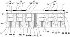
图1是根据本发明示例性实施例的发光元件俯视示意图;Fig. 1 is a schematic top view of a light emitting element according to an exemplary embodiment of the present invention;
图2是图1中沿B-B`的截面示意图;Fig. 2 is a schematic cross-sectional view along B-B' in Fig. 1;
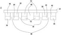
图3是根据示例性实施例的发光元件电极面示意图一;Fig. 3 is a first schematic diagram of an electrode surface of a light-emitting element according to an exemplary embodiment;
图4是根据示例性实施例的发光元件应用的电路板电极设计示意图;4 is a schematic diagram of a circuit board electrode design for light-emitting element applications according to an exemplary embodiment;
图5是根据示例性实施例的发光元件电极面示意图二;Fig. 5 is a second schematic diagram of an electrode surface of a light-emitting element according to an exemplary embodiment;
图6和图7是根据示例性实施例的发光元件的工艺过程截面示意图。6 and 7 are schematic cross-sectional views of a process of a light emitting element according to an exemplary embodiment.
附图标记:Reference signs:
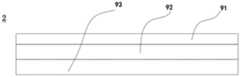
2-发光元件;10-第一LED子单元;20-第二LED子单元;30-第三LED子单元;11-第一半导体层;12-第一发光层;13第二半导体层;21-第三半导体层;22-第二发光层;23-第四半导体层;31-第五半导体层;32-第三发光层;33-第六半导体层;41-第一焊盘电极;42-第二焊盘电极;43-第三焊盘电极;44-第四焊盘电极;41a-第一焊接区域;42a-第二焊接区域;43a-第三焊接区域;44a-第四焊接区域;60-绝缘层;71-第一波长转换层;72第二波长转换层;73-阻隔层;81-第一沟槽;82-第二沟槽;83-共极沟槽;S1-第一表面;S2-第二表面;91-第一导电类型半导体层;92-发光层;93-第二导电类型半导体层。2-light-emitting element; 10-first LED subunit; 20-second LED subunit; 30-third LED subunit; 11-first semiconductor layer; 12-first light-emitting layer; 13 second semiconductor layer; 21 - the third semiconductor layer; 22 - the second light emitting layer; 23 - the fourth semiconductor layer; 31 - the fifth semiconductor layer; 32 - the third light emitting layer; 33 - the sixth semiconductor layer; 41 - the first pad electrode; 42 -second pad electrode; 43-third pad electrode; 44-fourth pad electrode; 41a-first welding area; 42a-second welding area; 43a-third welding area; 44a-fourth welding area ; 60-insulation layer; 71-first wavelength conversion layer; 72-second wavelength conversion layer; 73-barrier layer; 81-first groove; 82-second groove; 83-common pole groove; One surface; S2—the second surface; 91—the first conductivity type semiconductor layer; 92—the light emitting layer; 93—the second conductivity type semiconductor layer.
具体实施方式Detailed ways
为使本发明实施例的目的、技术方案和优点更加清楚,下面将结合本发明实施例中的附图,对本发明实施例中的技术方案进行清楚、完整地描述;下面所描述的本发明不同实施方式中所设计的技术特征只要彼此之间未构成冲突就可以相互结合。In order to make the purpose, technical solutions and advantages of the embodiments of the present invention clearer, the technical solutions in the embodiments of the present invention will be clearly and completely described below in conjunction with the accompanying drawings in the embodiments of the present invention; the present invention described below is different The technical features designed in the embodiments may be combined with each other as long as they do not constitute a conflict with each other.
在下文中,将参照附图详细描述本发明的示例性实施例。如在这里所使用的,根据示例性实施例的发光元件、LED子单元可以包括微型发光元件,该微型发光元件具有如本领域中已知的小于约10000平方μm的表面积。在其他示例性实施例中,根据特定应用,微型发光元件可以具有小于约4000平方μm或小于约2500平方μm的表面积。但本发明对于适用发光元件尺寸不做特殊限定。Hereinafter, exemplary embodiments of the present invention will be described in detail with reference to the accompanying drawings. As used herein, a light emitting element, an LED subunit, according to example embodiments may comprise a micro light emitting element having a surface area as known in the art of less than about 10000 square μm. In other exemplary embodiments, the micro light emitting elements may have a surface area of less than about 4000 square μm or less than about 2500 square μm, depending on the particular application. However, the present invention has no special limitation on the size of the applicable light-emitting element.
为达所述有点至少其中之一或其他优点,请参阅图1和图2,图1是根据示例性实施例的发光元件2的俯视示意图;图2是图1所示发光元件2沿B-B`的截面示意图。In order to achieve at least one of the above points or other advantages, please refer to FIG. 1 and FIG. 2. FIG. 1 is a schematic top view of a light-emitting
参照图1和图2,发光元件2包括具有在水平方向上平齐设置的第一LED子单元10、第二LED子单元20和第三LED子单元30的发光堆叠结构,以及与LED子单元10、20、30电性连接的第一焊盘电极41、第二焊盘电极42、第三焊盘电极43和第四焊盘电极44,发光元件2还包括绝缘层60,绝缘层60围绕覆盖发光堆叠结构的一侧以及各电极,定义发光堆叠结构背离绝缘层60的一面为第一表面S1,绝缘层60在背离发光堆叠结构的一侧形成有第二表面S2,在下文中,将以图示实施例的放置方位进行描述,也即第一表面S1位于发光堆叠结构的上侧或顶面,第二表面S2位于发光元件2的下侧或底面。各电极在内部与发光堆叠结构形成电性连接,并延伸至露出于第二表面S2形成焊接区域。Referring to FIG. 1 and FIG. 2, the
其中,虽然附图1和图2示出了包括三个LED子单元10、20和30的发光堆叠结构但是发明构思不限于形成在发光堆叠结构中的特定数量的LED子单元。例如,在一些示例性实施例中,发光堆叠结构可以在其中包括两个或更多个LED子单元。在下文中,将参照根据示例性实施例的包括三个LED子单元10、20和30的发光堆叠结构来描述发光元件2。Wherein, although FIGS. 1 and 2 illustrate a light emitting stack structure including three
在一些实施例中,发光堆叠结构可以形成于基板(图未示)上,基板可以包括透光绝缘材料以使光透过其。例如为蓝宝石Al2O3、GaN、SiC或玻璃等材料制成,但本发明的构思不限于此。本实施例中的发光元件2为发光堆叠结构脱离基板的状态进行详述。In some embodiments, the light emitting stack structure may be formed on a substrate (not shown in the figure), and the substrate may include a light-transmitting insulating material to allow light to pass therethrough. For example, it is made of materials such as sapphire Al2O3, GaN, SiC or glass, but the concept of the present invention is not limited thereto. The light-emitting
第一LED子单元10、第二LED子单元20和第三LED子单元30中的每个被构造为朝向第一表面S1发射光。在一些实施例中,第一LED子单元10、第二LED子单元20和第三LED子单元30中的每个可以采用不同的半导体材料制成,以使得第一LED子单元10、第二LED子单元20和第三LED子单元30中的每个的发光层可以发射的光可以具有彼此不相同的峰值波长的光。例如,第一LED子单元10、第二LED子单元20和第三LED子单元30可以分别发射蓝光、绿光和红光。然而,发明构思不限于此。作为另一示例,第一LED子单元10、第二LED子单元20和第三LED子单元30可以分别发射红光、绿光和蓝光。Each of the
第一LED子单元10包括依次层叠的第一半导体层11、第一发光层12和第二半导体层13。在一些实施例中,第一发光层12可以包括发射蓝光的半导体材料,例如氮化镓(GaN)、氮化铟镓(InGaN)和硒化锌(ZnSe),但不限于此。The
第二LED子单元20包括依次层叠的第三半导体层21、第二发光层22和第四半导体层23。在一些实施例中,第二发光层22可以包括发射绿光的半导体材料,例如氮化铟镓(InGaN)、氮化镓(GaN)、磷化镓(GaP)、磷化铝镓铟(AlGaInP)和磷化铝镓(AlGaP),但不限于此。The
第三LED子单元30包括依次层叠的第五半导体层31、第三发光层32和第六半导体层33。在一些实施例中,第三发光层32可以包括发射红光的半导体材料,例如砷化铝镓(AlGaAs)、磷砷化镓(GaAsP)、磷化铝镓铟(AlGaInP)和磷化镓(GaP),但不限于此。The
其中的第一半导体层11、第三半导体层21和第五半导体层31均为第一导电类型半导体;第二半导体层12、第四半导体层22和第六半导体层32均为第二导电类型半导体。以下对第一半导体层11、第三半导体层21或第五半导体层31简称为第一导电类型半导体,对第一发光层12、第二发光层22或第三发光层32简称为发光层,对第二半导体层12、第四半导体层22或第六半导体层32简称为第二导电类型半导体。根据示例性实施例,发光元件2的第一LED子单元10、第二LED子单元20和第三LED子单元30在水平方向上平齐设置也即第一半导体层11、所述第三半导体层21和所述第五半导体层31各自背离所述发光层的一面位于同一平面(第一表面S1)内。Wherein the
第一导电类型半导体可以为N型半导体,在电源作用下可以向发光层提供电子。在一些实施例中,第一导电类型半导体包括N型掺杂的氮化物层,磷化物层或者砷化物层。N型掺杂的氮化物层,磷化物或者砷化物可包括一个或多个IV族元素的N型杂质。N型杂质可以包括Si、Ge、Sn中的一种或其组合。The semiconductor of the first conductivity type can be an N-type semiconductor, which can provide electrons to the light-emitting layer under the action of a power supply. In some embodiments, the semiconductor of the first conductivity type includes an N-type doped nitride layer, phosphide layer or arsenide layer. The N-type doped nitride, phosphide or arsenide layer may include N-type impurities of one or more group IV elements. N-type impurities may include one of Si, Ge, Sn or a combination thereof.
发光层形成于第一导电类型半导体之上,发光层可以为量子阱结构(QuantumWell,简称QW)。在一些实施例中,发光层也可以为多重量子阱结构(Multiple QuantumWell,简称MQW),其中多重量子阱结构包括以重复的方式交替设置的多个量子阱层(Well)和多个量子阻障层(Barrier),例如可以是GaN/AlGaN、InAlGaN/InAlGaN、InGaN/AlGaN、GaInP/AlGaInP、GaInP/AlInP、InGaAS/AlInGaAS的多量子阱结构。此外,发光层内的阱层的组成以及厚度决定生成的光的波长。为了提高发光层的发光效率,可通过在发光层中改变量子阱的深度、成对的量子阱和量子势垒的层数、厚度和/或其它特征来实现。The light-emitting layer is formed on the semiconductor of the first conductivity type, and the light-emitting layer may be a quantum well structure (Quantum Well, QW for short). In some embodiments, the light-emitting layer can also be a multiple quantum well structure (Multiple QuantumWell, referred to as MQW), wherein the multiple quantum well structure includes multiple quantum well layers (Well) and multiple quantum barriers arranged alternately in a repeated manner. The layer (Barrier) may be, for example, a GaN/AlGaN, InAlGaN/InAlGaN, InGaN/AlGaN, GaInP/AlGaInP, GaInP/AlInP, InGaAS/AlInGaAS multi-quantum well structure. In addition, the composition and thickness of the well layer in the light emitting layer determine the wavelength of the generated light. In order to improve the luminous efficiency of the light-emitting layer, it can be realized by changing the depth of quantum wells, the number of pairs of quantum wells and quantum barriers, the thickness and/or other characteristics in the light-emitting layer.
第二导电类型半导体层为P型半导体层,在电源作用下可以向发光层提供空穴。在一些实施例中,第二导电类型半导体层包括P型掺杂的氮化物层,磷化物层或者砷化物层。P型掺杂的氮化物层,磷化物层或者砷化物层可包括一个或多个II族元素的P型杂质。P型杂质可以包括Mg、Zn、Be中的一种或其组合。第二导电类型半导体层可以是单层结构,也可以是多层结构,该多层结构具有不同的组成。此外,LED子单元10、20或30的设置不限于此,可以是依据实际需求来选择其它种类的LED子单元的结构。The second conductive type semiconductor layer is a P-type semiconductor layer, which can provide holes to the light-emitting layer under the action of a power supply. In some embodiments, the second conductivity type semiconductor layer includes a P-type doped nitride layer, phosphide layer or arsenide layer. The P-type doped nitride layer, phosphide layer or arsenide layer may include one or more P-type impurities of group II elements. The P-type impurities may include one of Mg, Zn, Be or a combination thereof. The second conductivity type semiconductor layer can be a single-layer structure or a multi-layer structure, and the multi-layer structures have different compositions. In addition, the arrangement of the
在一些实施例中,发光堆叠结构中的一个或更多个LED子单元可以采用相同的半导体材料制成,以使得第一LED子单元10、第二LED子单元20和第三LED子单元30可以发射具有基本相同峰值波长的光。例如在一些实施例中,第一LED子单元10、第二LED子单元20和第三LED子单元30各自的发光层可以均包括发射蓝光的半导体材料,例如氮化镓(GaN)、氮化铟镓(InGaN)和硒化锌(ZnSe),但不限于此。进一步地,为了使得该示例性实施例可以发出全色的光。在一些实施例中,如图1和图2所示,发光元件2还包括设置于第一表面S1之上的波长转换层,包括第一波长转换层710和第二波长转换层72。第一波长转换层71和第二波长转换层72分别与第一LED子单元10、第二LED子单元20和第三LED子单元30其中之二各自的发光层在第一表面S1上的正投影相重叠。波长转换层用于吸收从发光层发出的光并受激发射具有与发光层发射的光不同峰值波长的光,换言之,发光层的光经过波长转换层之后其光色发生了改变。In some embodiments, one or more LED subunits in the light emitting stack structure can be made of the same semiconductor material, so that the
在一些实施例中,波长转换层可以为荧光粉、荧光胶或者荧光陶瓷中的一种或者其中的任意组合。在另一实施例中,波长转换层可以为量子点材料。量子点,又可称为纳米晶,是一种由II-VI族或III-V族元素组成的纳米颗粒。量子点的粒径一般介于1-10nm之间,可适用于更小尺寸的微显示设备。量子点也具有电致发光与光致放光的效果。量子点在受激后可以发射荧光,发光颜色由材料和尺寸决定。因此可通过调控量子点粒径大小来改变其发光的波长。当量子点粒径越小,发光颜色越偏蓝色。当量子点粒径越大,发光颜色越偏红色。多种化学成分都可用于制作量子点。量子点的发光颜色可以覆盖从蓝光到红光的整个可见区。量子点具有高能力的吸光发光效率、很窄的半高宽、宽吸收频谱等特性,因此拥有很高的色彩纯度与饱和度。量子点具有结构简单,薄型化,可卷曲的优点,非常适用于微显示领域的应用。In some embodiments, the wavelength conversion layer may be one of phosphor powder, phosphor glue, or phosphor ceramic, or any combination thereof. In another embodiment, the wavelength conversion layer may be a quantum dot material. Quantum dots, also known as nanocrystals, are nanoparticles composed of II-VI or III-V elements. The particle size of quantum dots is generally between 1-10 nm, which can be applied to smaller-sized micro-display devices. Quantum dots also have electroluminescent and photoluminescent effects. Quantum dots can emit fluorescence after being excited, and the color of the light is determined by the material and size. Therefore, the wavelength of light emission can be changed by adjusting the particle size of quantum dots. The smaller the particle size of the quantum dots, the more blue the luminescent color. When the particle size of quantum dots is larger, the luminescent color is more reddish. A variety of chemical compositions can be used to make quantum dots. The emission color of quantum dots can cover the entire visible region from blue light to red light. Quantum dots have the characteristics of high light absorption and luminescence efficiency, narrow half-width, and wide absorption spectrum, so they have high color purity and saturation. Quantum dots have the advantages of simple structure, thinness, and rollability, and are very suitable for applications in the field of microdisplays.
在一些实施例中,波长转换层还可以包括第三波长转换层,以使得第一LED子单元10、第二LED子单元20和第三LED子单元各自发出的蓝光经过波长转换层后发射出三种不同色的光,以实现全色显示。In some embodiments, the wavelength conversion layer may further include a third wavelength conversion layer, so that the blue light emitted by the
在下文中,将以图示实施例中的发光元件2的结构为例进行详述,其第一波长转换层71设置于第二LED子单元20之上,第一波长转换层71吸收第二LED子单元20发射出的蓝光后例如可发射红光,第二波长转换层73设置于第三LED子单元30之上,第二波长转换层72吸收第三LED子单元发射出的蓝光后例如可发射绿光。第一LED子单元10之上设置有透明材料,以使得第一LED子单元10发射的蓝光可以透射出。第一LED子单元10与第一波长转换层71和第二波长转换层72共同实现RGB全色显示。In the following, the structure of the light-emitting
根据图示实施例,第一LED子单元10、第二LED子单元20和第三LED子单元30中的每个可以被独立地驱动。更具体地,每个LED子单元中各自的第一导电类型半导体和第二导电类型半导体中的一个可以被施加共电压,并且每个LED子单元的第一导电类型半导体和第二导电类型半导体中的另一个可以被施加相应的发光信号。例如,根据示出的示例性实施例,每个LED子单元的第一导电类型半导体可以是n型,每个LED子单元的第二导电类型半导体可以是p型。在下文中,根据示出的示例性实施例,第一导电类型半导体和第二导电类型半导体可以分别可互换地称为p型半导体层和n型半导体层。According to the illustrated embodiment, each of the
进一步的,通过第一焊盘电极41为每个LED子单元的n型半导体层施加共电压,分别通过第二焊盘电极42、第三焊盘电极43和第四焊盘电极44为第一LED子单元10、第二LED子单元20和第三LED子单元30的p型半导体层施加相应的发光信号。第一焊盘电极41与第一LED子单元10和第二LED子单元20以及第三LED子单元30各自的n型半导体层也即第一半导体层11、第三半导体层21和第五半导体层31均电性连接,第二焊盘电极42与第一LED子单元10的p型半导体层也即第二半导体层12电性连接,第三焊盘电极43与第二LED子单元20的p型半导体层也即第四半导体层22电性连接,第四焊盘电极44与第三LED子单元30的p型半导体层也即第六半导体层32电性连接。其中第一焊盘电极41、第二焊盘电极42、第三焊盘电极43以及第四焊盘电极44分别连接至露出于第二表面S2的第一焊接区域41a、第二焊接区域42a、第三焊接区域43a和第四焊接区域44a。通过该结构以实现LED子单元10、20和30中的每个可以被单独的驱动,同时具有n型共极的发光堆叠结构。Further, a common voltage is applied to the n-type semiconductor layer of each LED sub-unit through the
虽然根据图示实施例的发光元件2为n型共极的发光堆叠结构。但是本发明的构思不限于此。例如在一些实施例中,每个LED子单元的第一导电类型半导体可以为p型半导体层,第二导电类型半导体可以为n型半导体层,以形成具有p型共极的发光堆叠结构。以下将共同参照图示的n型共极的发光堆叠结构对发光元件2进行实例示例性说明。Although the light-emitting
根据示例性实施例,如图2所示,发光堆叠结构具有依次层叠的第一导电类型半导体层、发光层和第二导电类型半导体层,其中第一导电类型半导体层背离发光层的一面为第一表面S1,发光堆叠结构还具有自第二导电类型半导体层至第一导电类型半导体层的第一沟槽81和第二沟槽82,通过第一沟槽81和第二沟槽82将发光堆叠结构划分为三个区域,分别为第一LED子单元10、第二LED子单元20和第三LED子单元30。其中,第一沟槽81位于第一LED子单元10和第二LED子单元20之间,第二沟槽82位于第二LED子单元20和第三LED子单元30之间。According to an exemplary embodiment, as shown in FIG. 2 , the light emitting stack structure has a first conductive type semiconductor layer, a light emitting layer, and a second conductive type semiconductor layer stacked in sequence, wherein the side of the first conductive type semiconductor layer facing away from the light emitting layer is the second conductive type semiconductor layer. On a surface S1, the light-emitting stack structure also has a
在一些实施例中,第一沟槽81和第二沟槽82自第二导电类型半导体层背离发光层的一面向发光堆叠结构内部延伸并贯穿发光层后到第一导电类型半导体层邻近发光层的一面或者继续延伸至第一导电类型半导体层的内部。如此,第二导电类型半导体层被第一沟槽81和第二沟槽82划分为三个区域分别为第二半导体层13、第四半导体层23和第六半导体层33,发光层被第一沟槽81和第二沟槽82划分为三个区域分别为第一发光层12、第二发光层22和第三发光层32。第一导电类型半导体层并未被第一沟槽81和第二沟槽82贯穿,为一体结构,但是在第一表面S1的法向上观之,第一导电类型半导体层包括第一半导体层11、第三半导体层21和第五半导体层31。其中第一半导体层11与第一发光层12和第二半导体层13在第一表面S1上的正投影相重叠,共同构成了第一LED子单元10;第三半导体层21与第二发光层22和第四半导体层23在第一表面S1上的正投影相重叠,共同构成了第二LED子单元20;第五半导体层31与第三发光层32和第六半导体层33在第一表面S1上的正投影相重叠,共同构成了第三LED子单元30。In some embodiments, the
根据示例性实施例,在形成第一LED子单元10、第二LED子单元20和第三LED子单元30的过程中,通过对第一导电类型半导体层、发光层和第二导电类型半导体层的叠层结构进行蚀刻沟槽形成通过第一导电类型半导体层连接在一起的三个LED子单元的结构,三个LED子单元各自的一侧通过第一导电类型半导体层形成共极,另一侧则彼此之间形成阻隔以独立供电。在一些实施例中,沿第一表面S1的法向观之,第一沟槽81和第二沟槽82各自呈旋转对称的环形图案,第二沟槽82位于第一沟槽81的外围,因此形成第二LED子单元20围绕第一LED子单元10设置,第三LED子单元30围绕第二LED子单元20设置的结构,并且第第一LED子单元10、第二LED子单元20和第三LED子单元30各自的发光区域也即发光层呈旋转对称图形并且具有重叠的旋转中形。如此,当对发光元件2进行焊接时,将不必考虑发光层对于发光元件2需要统一方向排列的问题,例如即使若干发光元件2形成阵列时,其各自自身的旋转将不会对阵列的显示效果造成过多影响,有利于工艺简化。此外,但本发明的构思不限于第一发光层12、第二发光层22和第三发光层32必须为旋转对称图形,换言之,本发明的设计目的为各发光层处于发光元件2的中央,并且呈旋转对称图形以消除焊接时可能由于发光元件2自身的旋转影像显示效果的问题,但是允许在制程中由于制造公差,结构需要等原因在一定程度上破坏该旋转对称图形。According to an exemplary embodiment, in the process of forming the
在一些实施例中,发光堆叠结构还具有自第二导电类型半导体层至第一导电类型半导体层的共极沟槽83,如图2所示,共极沟槽83设置在第一LED子单元10的中央,贯穿了第二半导体层13和第一发光层12使得第一半导体层10背离第一表面S1的一侧暴露。第一焊盘电极41形成于共极沟槽83之中并且与第一半导体层10形成电性连接。较佳地,如图3所示,图3为根据示例性实施例的发光元件2的电极面示意图一,第一焊盘电极41位于第一LED子单元10的中央,并且其横截面形状呈旋转对称图形,例如正方形或者圆形。第一焊盘电极41自第一半导体层11延伸至第二表面S2露出第一焊接区域41a,在一些实施例中,第一焊盘电极41呈细长柱状结构,第一焊接区域41a呈旋转对称图形。In some embodiments, the light-emitting stack structure also has a
第二焊盘电极42形成于第二半导体层13外露的表面上并与第二半导体层13形成电性连接,较佳地,在一些实施例中,第二焊盘电极42包括形成于第二半导体层13上的若干个第二子焊盘电极,例如本实施例中为四个第二子焊盘电极,于第一表面S1的法向观之,如图3所示,四个第二子焊盘电极在第二半导体层13上呈旋转对称分布,各第二子焊盘电极自第二半导体层13的表面延伸至第二表面S2露出第二焊接区域42a,各第二子焊盘电极呈细长柱状结构,第二焊接区域42a呈旋转对称图形,并且其对称中心与第一焊接区域41a的相重叠。The
第三焊盘电极43形成于第二半导体层23外露的表面上并与第四半导体层23形成电性连接,较佳地,在一些实施例中,第三焊盘电极43包括形成于第四半导体层23上的若干个第三子焊盘电极,例如本实施例中为四个第三子焊盘电极,于第一表面S1的法向观之,如图3所示,四个第三子焊盘电极在第四半导体层23上呈旋转对称分布,各第三子焊盘电极自第四半导体层23的表面延伸至第二表面S2露出第三焊接区域43a,各第三子焊盘电极呈细长柱状结构,第三焊接区域43a呈旋转对称图形,并且其对称中心与第一焊接区域41a的相重叠。The
第四焊盘电极44形成于第六半导体层33外露的表面上并与第六半导体层33形成电性连接,较佳地,在一些实施例中,第四焊盘电极44包括形成于第六半导体层33上的若干个第四子焊盘电极,例如本实施例中为四个第四子焊盘电极,于第一表面S1的法向观之,如图3所示,四个第四子焊盘电极在第六半导体层33上呈旋转对称分布,各第四子焊盘电极自第六半导体层33的表面延伸至第二表面S2露出第四焊接区域44a,各第四子焊盘电极呈细长柱状结构,第四焊接区域44a呈旋转对称图形,并且其对称中心与第一焊接区域41a的相重叠。The
应当理解的是,根据上述示例性实施例,将本发明构思应用与正方形的发光元件2之上,形成阵列时,发光元件2需要被布置为矩形阵列,因此为了简化发光元件2的焊接工艺,上述关于示例性实施例中的旋转对称图形的旋转角为90度或者180度,较佳地为90度,使得发光元件2在四个方向上均可以被正确焊接连接,当对数十万或数百万个发光元件2进行焊接时,完成的样品经过乱数搅拌后可以焊接到PCB 板上,PCB板的电极设计如图4所示,一共有4个焊盘C、B、G、R,分别和第一焊盘电极41,第二焊盘电极42,第三焊盘电极43和第四焊盘电极44对应。如此,发光元件2只需要区分正反面,不需要区分方向即可焊接。但是本发明构思不限于对正方形发光元件的应用,因此旋转对称图形的旋转角也可以进行调整,例如当发光元件为六角密堆结构阵列时,该旋转角可以取值为60度。It should be understood that, according to the above exemplary embodiments, when the concept of the present invention is applied to square light-emitting
但本发明对于发光元件2的电极焊接区域的设计构思不限于此,如图5所示,图5为根据示例性实施例的发光元件2的电极面示意图二,可以在绝缘层60中设置连接电极(图未示),连接电极包括与第一半导体层11电性连接的第一连接电极、与第二半导体层13电性连接的第二连接电极、与第四半导体层23电性连接的第三连接电极以及与第六半导体层33电性连接的第四连接电极,第一焊盘电极41设置在第一连接电极之上并且部分与第一连接电极相重叠接触,第二焊盘电极42设置在第二连接电极之上并且部分与第二连接电极相重叠接触,第三焊盘电极43设置在第三连接电极之上并且部分与第三连接电极相重叠接触,第四焊盘电极44设置在第四连接电极之上并且部分与第四连接电极相重叠接触。以发光元件2的中心点为原点建立平面坐标系,在如图5所示的实施例中,第一焊盘电极41位于坐标系的第一象限,第二焊盘电极42位于坐标系的第二象限,第三焊盘电极位于坐标系的第三象限,第四焊盘电极44位于坐标系的第四象限,并且使得外露于第二表面S2的第一焊接区域41a、第二焊接区域42a、第三焊接区域43a和第四焊接区域44a呈如图5所示的分布,使得四者共同形成的图案呈旋转对称图形。较佳地,在一些实施例中,为了便于形成该分布结构的各焊盘电极,第一LED子单元10、第二LED子单元20和第三LED子单元30各自可以为包括相嵌套的三个矩形或者圆形以及相适应形状的环状结构,以使得各焊盘电极在第一表面S1的法向上可以与对应的LED子单元具有重叠区域,以便于连接电极和焊盘电极的制作。However, the design concept of the present invention for the electrode welding area of the
在一些实施例中,绝缘层60覆盖发光堆叠结构设置有焊盘电极的一侧,绝缘层60填充于第一沟槽81和第二沟槽82之中以隔绝第一LED子单元10、第二LED子单元20和第三LED子单元30之间的连接电连接,以防止发生串电。此外,绝缘层60根据涉及的位置具有不同的功效,例如覆盖发光堆叠结构的侧壁,可防止因导电材料泄露而电连通第一导电类型半导体层和第二导电类型半导体层,以减少LED子单元的短路异常等。绝缘层60的材料包含非导电材料。非导电材料优选地为无机材料或是介电材料。无机材料可以包含硅胶(Silicone)。介电材料包含氧化铝(AlO)、氮化硅(SiNx)、氧化硅(SiOx)、氧化钛(TiOx)、或氟化镁(MgFx)可以是电绝缘材料。例如,绝缘层60可以是二氧化硅、氮化硅、氧化钛、氧化钽、氧化铌、钛酸钡或者其组合,其组合例如可以是两种材料重复堆叠形成的布拉格反射镜(DBR)。In some embodiments, the insulating
根据示例性实施例中,如图1所示,发光元件2还包括设置在第一波长转换层71和第二波长转换层72之间的间隙中的阻隔层73。较佳地,阻隔层73可以为用于吸收光的黑色膜层,具体优选为可以为由粒径不大于1μm黑色填充成分分散于硅胶、环氧树脂、聚酰亚胺、低温玻璃、聚硅氧烷、聚硅氮烷等透明或者半透明的材料中而形成的黑色膜层,其中的黑色填充成分包括但不限于是炭黑、氮化钛、氧化铁、四氧化三铁、铁粉等。在一些实施例中,阻隔层73还可以为黑色填充成分的粒径范围优选为10~100nm,或者100~200nm,或者200~300nm,或者300nm~500nm。黑色填充成分也可采用黑色染料。以削弱串光带来的影响,使得波长转换层尽量由与其相对的LED子单元发出的光激发,提高发光元件2的个LED子单元的独立驱动效果,增加发出色光的准确度辨识度。较佳地,在一些实施例中,还可以于第一沟槽81和第二沟槽82各自的侧壁之上设置阻隔层73,以进一步的提高色光的阻隔效果。此外,阻隔层73还可以设置在第一波长转换层71和第一LED子单元10之上的透明材料之间的间隙中。According to an exemplary embodiment, as shown in FIG. 1 , the
此外,当发光元件2被安装到另一基底以制造显示装置时,例如,由于发光芯片100的堆叠结构,与传统发光器件相比,待安装的芯片的数量可以被显著减少。如此,采用发光元件1的显示装置的制造可以被显著简化,特别是当在一个显示装置中形成数十万或数百万个像素时。如此,通过对LED子单元10、20、30的堆叠结构设计和各电极的焊接区域以及发光区域的旋转对称化使得发光元件2在后续的制造使用过程中被显著简化。In addition, when the
在下文中,将参照附图描述根据图2和图3所示的示例性实施例的发光元件2的形成过程。Hereinafter, a process of forming the
参照图6,可以通过例如金属有机化学气相沉积(MOCVD)法或分子束4外延(MBE)法分别生长第一导电类型半导体层91、发光层92和第二导电类型半导体层93以形成发光堆叠结构的初始外延。Referring to FIG. 6, a first conductive
参照图7,经由蚀刻工艺使得第一导电类型半导体层91、发光层92和第二导电类型半导体层93组成的发光堆叠结构的部分图案化,第一沟槽81、第二沟槽82和共极沟槽83。将发光堆叠结构通过第一沟槽81和第二沟槽82划分为第一LED子单元10、第二LED子单元20和第三LED子单元30。并使得第一发光层12、第二发光层22和第三发光层32各自呈旋转对称图形,且具有重叠的旋转中心。Referring to FIG. 7, the partial patterning of the light emitting stack structure composed of the first conductivity
返回参照图2,分别在共极沟槽83露出的第一半导体层11的表面、第二半导体层13、第四半导体层23和第六半导体层33的表面形成第一焊盘电极41、第二焊盘电极42、第三焊盘电极43和第四焊盘电极44,并且使得第一焊接区域41a、第二焊接区域42a、第三焊接区域43a和第四焊接区域44a各自呈旋转对称图形并且具有重叠的旋转中心。具体地,在发光堆叠结构体上将种子层作为导电性表面而被沉积,并且可以在将要形成焊盘电极的位置暴露种子层的方式形成光刻胶图案。种子层可以沉积为月1000埃的厚度,但是并不限于此。随后种子层可以被诸如Cu、Ni、Ti、Sb、Zn、Mo、Co、Sn、Ag的金属或者这些金属的合金镀覆,并且残留的光刻胶图案以及种子层可以被去除。在一些示例性实施例中,可以通过化学镀镍浸金(ENIG)等将附加金属沉积或镀覆在焊盘电极上,以防止或至少抑制电极的氧化。Referring back to FIG. 2, the
接着,在发光堆叠结构背离第一表面S1的一侧形成绝缘层60,绝缘层60填充于第一沟槽81和第二沟槽82以及共极沟槽83与第一焊盘电极41之间的间隙中,并且覆盖各焊盘电极的侧面。绝缘层60可以通过抛光工艺等形成为与焊盘电极41、42、43和44的顶面基本齐平的第二表面S2,较佳地,焊盘电极41、42、43和44的顶面可以略凸出于第二表面S2。根据示例性实施例,绝缘层60可以包括黑色环氧树脂模塑料(EMC),但不限于此。例如,在一些示例性实施例中,绝缘层60可以包括具有光敏性的聚酰亚胺(PID)干膜。以此方式,绝缘层60可以保护发光结构免受可能会在后续工艺期间施加的外部冲击的影响,以及向发光元件2提供足够的接触面积以有助于其在后续转移步骤期间的处理。此外,绝缘层60可以防止光朝向发光元件2的侧表面泄漏,以防止或至少抑制从相邻发光元件2发射的光的干扰。Next, an insulating
然后,在第一表面S1之上形成第一波长转换层71和第二波长转换层72以及透明材料,使得透明材料位于第一LED子单元10之上,第一波长转换层71位于第二LED子单元20之上,第二波长转换层72位于第三LED子单元30之上。并且于第一波长转换层71分别与第二波长转换层72和透明材料之间的间隙中形成阻隔层73。Then, a first
最后应说明的是:以上各实施例仅用以说明本发明的技术方案,而非对其限制;尽管参照前述各实施例对本发明进行了详细的说明,本领域的普通技术人员应当理解:其依然可以对前述各实施例所记载的技术方案进行修改,或者对其中部分或者全部技术特征进行等同替换;而这些修改或者替换,并不使相应技术方案的本质脱离本发明各实施例技术方案的范围。Finally, it should be noted that: the above embodiments are only used to illustrate the technical solutions of the present invention, rather than limiting them; although the present invention has been described in detail with reference to the foregoing embodiments, those of ordinary skill in the art should understand that: It is still possible to modify the technical solutions described in the foregoing embodiments, or perform equivalent replacements for some or all of the technical features; and these modifications or replacements do not make the essence of the corresponding technical solutions deviate from the technical solutions of the various embodiments of the present invention. scope.
Claims (19)
Translated fromChinesePriority Applications (1)
| Application Number | Priority Date | Filing Date | Title |
|---|---|---|---|
| CN202210862401.2ACN115274637A (en) | 2022-07-20 | 2022-07-20 | Light-emitting element and light-emitting device |
Applications Claiming Priority (1)
| Application Number | Priority Date | Filing Date | Title |
|---|---|---|---|
| CN202210862401.2ACN115274637A (en) | 2022-07-20 | 2022-07-20 | Light-emitting element and light-emitting device |
Publications (1)
| Publication Number | Publication Date |
|---|---|
| CN115274637Atrue CN115274637A (en) | 2022-11-01 |
Family
ID=83768068
Family Applications (1)
| Application Number | Title | Priority Date | Filing Date |
|---|---|---|---|
| CN202210862401.2APendingCN115274637A (en) | 2022-07-20 | 2022-07-20 | Light-emitting element and light-emitting device |
Country Status (1)
| Country | Link |
|---|---|
| CN (1) | CN115274637A (en) |
Cited By (2)
| Publication number | Priority date | Publication date | Assignee | Title |
|---|---|---|---|---|
| CN117995871A (en)* | 2024-04-03 | 2024-05-07 | 镭昱光电科技(苏州)有限公司 | Display device and method for manufacturing the same |
| CN118073395A (en)* | 2024-04-19 | 2024-05-24 | 镭昱光电科技(苏州)有限公司 | Display device and method for manufacturing the same |
Citations (5)
| Publication number | Priority date | Publication date | Assignee | Title |
|---|---|---|---|---|
| US20070034884A1 (en)* | 2005-08-11 | 2007-02-15 | Micron Technology, Inc. | Pixel cells in a honeycomb arrangement |
| CN104124263A (en)* | 2013-04-26 | 2014-10-29 | 三星显示有限公司 | Organic light emitting diode display |
| CN208077981U (en)* | 2018-02-09 | 2018-11-09 | 京东方科技集团股份有限公司 | pixel arrangement structure, display panel, high-precision metal mask plate and display device |
| CN110133886A (en)* | 2018-02-09 | 2019-08-16 | 京东方科技集团股份有限公司 | Pixel arrangement structure, display substrate and display device |
| CN111384293A (en)* | 2018-12-31 | 2020-07-07 | 乐金显示有限公司 | LED display device |
- 2022
- 2022-07-20CNCN202210862401.2Apatent/CN115274637A/enactivePending
Patent Citations (5)
| Publication number | Priority date | Publication date | Assignee | Title |
|---|---|---|---|---|
| US20070034884A1 (en)* | 2005-08-11 | 2007-02-15 | Micron Technology, Inc. | Pixel cells in a honeycomb arrangement |
| CN104124263A (en)* | 2013-04-26 | 2014-10-29 | 三星显示有限公司 | Organic light emitting diode display |
| CN208077981U (en)* | 2018-02-09 | 2018-11-09 | 京东方科技集团股份有限公司 | pixel arrangement structure, display panel, high-precision metal mask plate and display device |
| CN110133886A (en)* | 2018-02-09 | 2019-08-16 | 京东方科技集团股份有限公司 | Pixel arrangement structure, display substrate and display device |
| CN111384293A (en)* | 2018-12-31 | 2020-07-07 | 乐金显示有限公司 | LED display device |
Cited By (3)
| Publication number | Priority date | Publication date | Assignee | Title |
|---|---|---|---|---|
| CN117995871A (en)* | 2024-04-03 | 2024-05-07 | 镭昱光电科技(苏州)有限公司 | Display device and method for manufacturing the same |
| CN118073395A (en)* | 2024-04-19 | 2024-05-24 | 镭昱光电科技(苏州)有限公司 | Display device and method for manufacturing the same |
| CN118073395B (en)* | 2024-04-19 | 2024-08-09 | 镭昱光电科技(苏州)有限公司 | Display device and method for manufacturing the same |
Similar Documents
| Publication | Publication Date | Title |
|---|---|---|
| US12356783B2 (en) | Light emitting device for display and unit pixel having the same | |
| CN102024891B (en) | Light-emitting element | |
| US20250063877A1 (en) | Led display panel and led display apparatus having the same | |
| CN114616674A (en) | LED display device | |
| JP7460650B2 (en) | Light-emitting element for display and display device having same | |
| CN110071202A (en) | Miniature LED element and image-displaying member | |
| US20240429346A1 (en) | Light emitting device for display and display apparatus having the same | |
| KR102752397B1 (en) | Light-emitting element for display and display device having the same | |
| CN109417082A (en) | Semiconductor devices and display device including semiconductor devices | |
| CN110265586A (en) | Display panel and manufacturing method thereof | |
| JP2024180401A (en) | Light emitting device for display and light emitting package having the same | |
| CN212934611U (en) | display device | |
| CN115274637A (en) | Light-emitting element and light-emitting device | |
| US20240282803A1 (en) | Light emitting device for display and display apparatus having the same | |
| US20220131055A1 (en) | Light source device, display device and manufacturing method of light source device | |
| CN110311053A (en) | Display panel and manufacturing method thereof | |
| CN117352625A (en) | MicroLED microdisplay chip and preparation method | |
| CN114600239A (en) | Light emitting element for display and LED display device having the same | |
| US20230155062A1 (en) | Package structure and forming method thereof | |
| KR20170133758A (en) | Light emitting device | |
| CN114600240A (en) | Display light-emitting element and LED display device having the same | |
| US11742377B2 (en) | Light emitting diode chip, display device and method for manufacturing the same | |
| CN118676287B (en) | Micro-LED display chip, display device and manufacturing method | |
| CN212412081U (en) | Light-emitting element for display and display device having the same | |
| CN209929308U (en) | Display panel |
Legal Events
| Date | Code | Title | Description |
|---|---|---|---|
| PB01 | Publication | ||
| PB01 | Publication | ||
| SE01 | Entry into force of request for substantive examination | ||
| SE01 | Entry into force of request for substantive examination |