CN115268765A - Nandflash autonomous bad block management method and system based on FPGA - Google Patents
Nandflash autonomous bad block management method and system based on FPGADownload PDFInfo
- Publication number
- CN115268765A CN115268765ACN202210666041.9ACN202210666041ACN115268765ACN 115268765 ACN115268765 ACN 115268765ACN 202210666041 ACN202210666041 ACN 202210666041ACN 115268765 ACN115268765 ACN 115268765A
- Authority
- CN
- China
- Prior art keywords
- bad block
- nandflash
- block
- index number
- fpga
- Prior art date
- Legal status (The legal status is an assumption and is not a legal conclusion. Google has not performed a legal analysis and makes no representation as to the accuracy of the status listed.)
- Pending
Links
Images

Classifications
- G—PHYSICS
- G06—COMPUTING OR CALCULATING; COUNTING
- G06F—ELECTRIC DIGITAL DATA PROCESSING
- G06F3/00—Input arrangements for transferring data to be processed into a form capable of being handled by the computer; Output arrangements for transferring data from processing unit to output unit, e.g. interface arrangements
- G06F3/06—Digital input from, or digital output to, record carriers, e.g. RAID, emulated record carriers or networked record carriers
- G06F3/0601—Interfaces specially adapted for storage systems
- G06F3/0628—Interfaces specially adapted for storage systems making use of a particular technique
- G06F3/0638—Organizing or formatting or addressing of data
- G06F3/064—Management of blocks
- G—PHYSICS
- G06—COMPUTING OR CALCULATING; COUNTING
- G06F—ELECTRIC DIGITAL DATA PROCESSING
- G06F12/00—Accessing, addressing or allocating within memory systems or architectures
- G06F12/02—Addressing or allocation; Relocation
- G06F12/08—Addressing or allocation; Relocation in hierarchically structured memory systems, e.g. virtual memory systems
- G06F12/0802—Addressing of a memory level in which the access to the desired data or data block requires associative addressing means, e.g. caches
- G06F12/0877—Cache access modes
- G06F12/0882—Page mode
- G—PHYSICS
- G06—COMPUTING OR CALCULATING; COUNTING
- G06F—ELECTRIC DIGITAL DATA PROCESSING
- G06F3/00—Input arrangements for transferring data to be processed into a form capable of being handled by the computer; Output arrangements for transferring data from processing unit to output unit, e.g. interface arrangements
- G06F3/06—Digital input from, or digital output to, record carriers, e.g. RAID, emulated record carriers or networked record carriers
- G06F3/0601—Interfaces specially adapted for storage systems
- G06F3/0602—Interfaces specially adapted for storage systems specifically adapted to achieve a particular effect
- G06F3/0604—Improving or facilitating administration, e.g. storage management
- G—PHYSICS
- G06—COMPUTING OR CALCULATING; COUNTING
- G06F—ELECTRIC DIGITAL DATA PROCESSING
- G06F3/00—Input arrangements for transferring data to be processed into a form capable of being handled by the computer; Output arrangements for transferring data from processing unit to output unit, e.g. interface arrangements
- G06F3/06—Digital input from, or digital output to, record carriers, e.g. RAID, emulated record carriers or networked record carriers
- G06F3/0601—Interfaces specially adapted for storage systems
- G06F3/0628—Interfaces specially adapted for storage systems making use of a particular technique
- G06F3/0646—Horizontal data movement in storage systems, i.e. moving data in between storage devices or systems
- G06F3/0652—Erasing, e.g. deleting, data cleaning, moving of data to a wastebasket
- G—PHYSICS
- G06—COMPUTING OR CALCULATING; COUNTING
- G06F—ELECTRIC DIGITAL DATA PROCESSING
- G06F3/00—Input arrangements for transferring data to be processed into a form capable of being handled by the computer; Output arrangements for transferring data from processing unit to output unit, e.g. interface arrangements
- G06F3/06—Digital input from, or digital output to, record carriers, e.g. RAID, emulated record carriers or networked record carriers
- G06F3/0601—Interfaces specially adapted for storage systems
- G06F3/0628—Interfaces specially adapted for storage systems making use of a particular technique
- G06F3/0655—Vertical data movement, i.e. input-output transfer; data movement between one or more hosts and one or more storage devices
- G06F3/0656—Data buffering arrangements
Landscapes
- Engineering & Computer Science (AREA)
- Theoretical Computer Science (AREA)
- Physics & Mathematics (AREA)
- General Engineering & Computer Science (AREA)
- General Physics & Mathematics (AREA)
- Human Computer Interaction (AREA)
- Techniques For Improving Reliability Of Storages (AREA)
Abstract
Translated fromChinese
Description
Translated fromChinese技术领域technical field
本发明涉及坏块管理技术领域,具体地,涉及一种基于FPGA的Nandflash自主坏块管理方法和系统。The invention relates to the technical field of bad block management, in particular to an FPGA-based Nandflash autonomous bad block management method and system.
背景技术Background technique
星载计算机常用CPU和FPGA为核心架构共同完成星上存储和控制等功能。以往的功能框架中,Nandflash作为存储器件,其擦除、读写等接口逻辑控制由FPGA来完成,CPU则完成存储数据的控制和Nandflash的可靠性控制(冗余设计或者坏块管理)。On-board computers usually use CPU and FPGA as the core architecture to jointly complete functions such as on-board storage and control. In the previous functional framework, Nandflash was used as a storage device, and its interface logic control such as erasing, reading and writing was completed by FPGA, and the CPU completed the control of stored data and the reliability control of Nandflash (redundant design or bad block management).
专利文献CN104765695A(申请号:CN201510158107.3)公开了一种NAND FLASH坏块管理系统,包括NAND FLASH接口控制单元、坏块管理单元、非易失性存储器接口控制单元和非易失性存储器,所述NAND FLASH接口控制单元连接NAND FLASH阵列,所述NAND FLASH接口控制单元连接坏块管理单元,所述坏块管理单元通过非易失性存储器接口控制单元连接非易失性存储器。所述的非易失性存储器是EEPROM。所述的坏块管理单元基于FPGA。Patent document CN104765695A (application number: CN201510158107.3) discloses a NAND FLASH bad block management system, including a NAND FLASH interface control unit, a bad block management unit, a non-volatile memory interface control unit and a non-volatile memory. The NAND FLASH interface control unit is connected to the NAND FLASH array, the NAND FLASH interface control unit is connected to the bad block management unit, and the bad block management unit is connected to the nonvolatile memory through the nonvolatile memory interface control unit. The non-volatile memory is EEPROM. The bad block management unit is based on FPGA.
随着星上功能需求越来越复杂,CPU的工作负担也越来越重,将坏块管理移到FPGA中来实现,既给CPU减负,使其能更好地完成其他系统级的任务,又充分利用了FPGA快速响应,并行处理的优点,高效可靠地完成Nandflash的存储回放功能。本发明解决的是星上Nandflash如何在FPGA中实现坏块出厂检索、坏块信息维护、块地址动态映射等功能的具体问题。As the functional requirements on the star become more and more complex, the workload of the CPU is also getting heavier. Moving the management of bad blocks to the FPGA will not only reduce the burden on the CPU, but also enable it to better complete other system-level tasks. It also makes full use of the advantages of fast response and parallel processing of FPGA to efficiently and reliably complete the storage and playback function of Nandflash. The invention solves the specific problem of how to implement functions such as retrieval of bad blocks at the factory, maintenance of bad block information, dynamic mapping of block addresses and the like in the FPGA of the Nandflash on the star.
发明内容Contents of the invention
针对现有技术中的缺陷,本发明的目的是提供一种基于FPGA的Nandflash自主坏块管理方法和系统。Aiming at the defects in the prior art, the purpose of the present invention is to provide a kind of FPGA-based Nandflash autonomous bad block management method and system.
根据本发明提供的基于FPGA的Nandflash自主坏块管理方法,包括:According to the FPGA-based Nandflash autonomous bad block management method provided by the present invention, comprising:
步骤1:在芯片出厂时,进行坏块出厂检索;Step 1: When the chip leaves the factory, perform a factory retrieval of bad blocks;
步骤2:对坏块信息进行维护;Step 2: Maintain bad block information;
步骤3:进行块地址映射;Step 3: Perform block address mapping;
步骤4:对Nandflash接口进行互斥调度。Step 4: Execute mutual exclusion scheduling on the Nandflash interface.
优选的,所述步骤1包括:Preferably, said step 1 includes:
在每个坏块的第一页进行标记,标记位置为Byte4096,标记值为0x00,正常值为0xFF;Mark the first page of each bad block, the mark position is Byte4096, the mark value is 0x00, and the normal value is 0xFF;
在芯片初始化之后,擦除编程之前,对Nandflash的所有块进行遍历检索;再将检索到0x00对应的块索引号信息存入非坏块block0中。After the chip is initialized and before erasing and programming, traverse and retrieve all the blocks of Nandflash; then store the retrieved block index number information corresponding to 0x00 into the non-bad block block0.
优选的,所述步骤2包括:Preferably, said step 2 includes:
步骤2.1:开辟一块BLOCK RAM空间用于缓存和更新坏块列表信息,将block0中的坏块索引号搬移到随机存取存储器RAM中,以便地址映射时使用;Step 2.1: Open up a BLOCK RAM space for caching and updating the bad block list information, and move the bad block index number in block0 to the random access memory RAM for use in address mapping;
步骤2.2:在固存操作的过程中,擦除或者页编程后进行状态读取,根据器件手册,读出状态字bit0为1时,表明该操作失败,认为有新增坏块,按照芯片出厂的方式对该块的第一页Byte4096写入0x00,作为坏块信息的标记,标记完成后重新遍历坏块,更新block0中的坏块信息。Step 2.2: In the process of solid storage operation, read the status after erasing or page programming. According to the device manual, when the status word bit0 is read as 1, it indicates that the operation failed, and it is considered that there is a new bad block. According to the chip factory The method writes 0x00 to Byte4096 of the first page of the block as a mark of the bad block information. After the mark is completed, it traverses the bad block again and updates the bad block information in block0.
优选的,所述步骤3包括:在BlockRAM中按地址从低到高存储坏块索引号的信息,且RAM初始化填充全1数据,在模块工作时,按地址从0开始读出数据,原块索引号与之比较,如果大于等于RAM的数据输出Dout,则将读地址加1,继续循环比较,直到小于Dout时停止循环,最终映射的索引号就是原块索引号加上RAM的读地址再加1。Preferably, the step 3 includes: storing the information of the bad block index number in the BlockRAM from low to high according to the address, and the RAM is initialized and filled with all 1 data, and when the module is working, the data is read from 0 according to the address, and the original block The index number is compared with it, if it is greater than or equal to the data output Dout of RAM, then add 1 to the read address, and continue the cycle comparison until it is less than Dout, stop the loop, and the final mapped index number is the original block index number plus the read address of RAM. plus 1.
优选的,所述步骤4包括:Preferably, said step 4 includes:
步骤4.1:通过FPGA设置通道号轮询,接收访问请求;Step 4.1: Set channel number polling through FPGA to receive access request;
步骤4.2:当前通道空闲时,响应访问请求,给出访问应答,此时该通道占用Nandflash使用权限;Step 4.2: When the current channel is idle, respond to the access request and give an access response. At this time, the channel occupies the Nandflash usage authority;
步骤4.3:当Nandflash操作完成时,释放当前通道的使用权限。Step 4.3: When the Nandflash operation is completed, release the usage permission of the current channel.
根据本发明提供的基于FPGA的Nandflash自主坏块管理系统,包括:According to the FPGA-based Nandflash autonomous bad block management system provided by the present invention, comprising:
模块M1:在芯片出厂时,进行坏块出厂检索;Module M1: When the chip leaves the factory, perform bad block retrieval;
模块M2:对坏块信息进行维护;Module M2: maintain bad block information;
模块M3:进行块地址映射;Module M3: perform block address mapping;
模块M4:对Nandflash接口进行互斥调度。Module M4: perform mutual exclusion scheduling on the Nandflash interface.
优选的,所述模块M1包括:Preferably, the module M1 includes:
在每个坏块的第一页进行标记,标记位置为Byte4096,标记值为0x00,正常值为0xFF;Mark the first page of each bad block, the mark position is Byte4096, the mark value is 0x00, and the normal value is 0xFF;
在芯片初始化之后,擦除编程之前,对Nandflash的所有块进行遍历检索;再将检索到0x00对应的块索引号信息存入非坏块block0中。After the chip is initialized and before erasing and programming, traverse and retrieve all the blocks of Nandflash; then store the retrieved block index number information corresponding to 0x00 into the non-bad block block0.
优选的,所述模块M2包括:Preferably, the module M2 includes:
模块M2.1:开辟一块BLOCK RAM空间用于缓存和更新坏块列表信息,将block0中的坏块索引号搬移到随机存取存储器RAM中,以便地址映射时使用;Module M2.1: Open up a BLOCK RAM space for caching and updating bad block list information, and move the bad block index number in block0 to random access memory RAM for use in address mapping;
模块M2.2:在固存操作的过程中,擦除或者页编程后进行状态读取,根据器件手册,读出状态字bit0为1时,表明该操作失败,认为有新增坏块,按照芯片出厂的方式对该块的第一页Byte4096写入0x00,作为坏块信息的标记,标记完成后重新遍历坏块,更新block0中的坏块信息。Module M2.2: In the process of solid storage operation, read the status after erasing or page programming. According to the device manual, when the read status word bit0 is 1, it indicates that the operation failed, and it is considered that there is a new bad block. According to The way the chip leaves the factory writes 0x00 to Byte4096 of the first page of the block as a mark of bad block information. After the marking is completed, it traverses the bad block again and updates the bad block information in block0.
优选的,所述模块M3包括:在BlockRAM中按地址从低到高存储坏块索引号的信息,且RAM初始化填充全1数据,在模块工作时,按地址从0开始读出数据,原块索引号与之比较,如果大于等于RAM的数据输出Dout,则将读地址加1,继续循环比较,直到小于Dout时停止循环,最终映射的索引号就是原块索引号加上RAM的读地址再加1。Preferably, the module M3 includes: storing bad block index number information in the BlockRAM according to the address from low to high, and the RAM is initialized and filled with all 1 data, and when the module is working, the data is read from 0 according to the address, the original block The index number is compared with it, if it is greater than or equal to the data output Dout of RAM, then add 1 to the read address, and continue the cycle comparison until it is less than Dout, stop the loop, and the final mapped index number is the original block index number plus the read address of RAM. plus 1.
优选的,所述模块M4包括:Preferably, the module M4 includes:
模块M4.1:通过FPGA设置通道号轮询,接收访问请求;Module M4.1: Set channel number polling through FPGA and receive access request;
模块M4.2:当前通道空闲时,响应访问请求,给出访问应答,此时该通道占用Nandflash使用权限;Module M4.2: When the current channel is idle, it responds to the access request and gives an access response. At this time, the channel occupies the Nandflash usage authority;
模块M4.3:当Nandflash操作完成时,释放当前通道的使用权限。Module M4.3: When the Nandflash operation is completed, release the usage permission of the current channel.
与现有技术相比,本发明具有如下的有益效果:Compared with the prior art, the present invention has the following beneficial effects:
(1)本发明将坏块管理移到FPGA中来实现,既给CPU减负,使其能更好地完成其他系统级的任务,又充分利用了FPGA快速响应,并行处理的优点,高效可靠地完成Nandflash的存储回放功能;(1) The present invention moves bad block management to FPGA to realize, not only reduces the burden to CPU, makes it can finish other system-level tasks better, makes full use of FPGA fast response again, the advantage of parallel processing, efficient and reliable Complete the storage and playback function of Nandflash;
(2)本发明解决了星上Nandflash如何在FPGA中实现坏块出厂检索、坏块信息维护、块地址动态映射等功能的具体问题。(2) The present invention solves the specific problem of how to implement functions such as bad block retrieval, bad block information maintenance, and block address dynamic mapping in the FPGA on the Nandflash on the star.
附图说明Description of drawings
通过阅读参照以下附图对非限制性实施例所作的详细描述,本发明的其它特征、目的和优点将会变得更明显:Other characteristics, objects and advantages of the present invention will become more apparent by reading the detailed description of non-limiting embodiments made with reference to the following drawings:
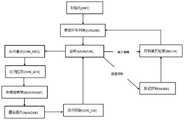
图1为本发明工作流程图;Fig. 1 is a work flow chart of the present invention;
图2为块地址映射工作原理图。Figure 2 is a working principle diagram of block address mapping.
具体实施方式Detailed ways
下面结合具体实施例对本发明进行详细说明。以下实施例将有助于本领域的技术人员进一步理解本发明,但不以任何形式限制本发明。应当指出的是,对本领域的普通技术人员来说,在不脱离本发明构思的前提下,还可以做出若干变化和改进。这些都属于本发明的保护范围。The present invention will be described in detail below in conjunction with specific embodiments. The following examples will help those skilled in the art to further understand the present invention, but do not limit the present invention in any form. It should be noted that those skilled in the art can make several changes and improvements without departing from the concept of the present invention. These all belong to the protection scope of the present invention.
实施例:Example:
本发明除了实现Nandflash(Nand闪存,是flash存储器的一种)基本的初始化、擦除、页编程、页读取等基本接口时序外,还要完成坏块管理及相关的功能:In addition to realizing the basic interface timings of Nandflash (Nand flash memory, which is a kind of flash memory), the present invention also needs to complete bad block management and related functions:
(1)坏块出厂检索;(1) Bad block factory retrieval;
(2)坏块信息维护;(2) Bad block information maintenance;
(3)块地址映射;(3) Block address mapping;
(4)Nandflash接口的互斥调度。(4) Mutual exclusion scheduling of Nandflash interface.
本发明工作流程图框图如图1所示,本发明具体方法分成以下几个步骤:As shown in Figure 1, the block diagram of the work flow chart of the present invention, the specific method of the present invention is divided into the following steps:
1、坏块遍历检索(BBCHK);1. Bad block traversal retrieval (BBCHK);
以MT29F8G08为例,芯片出厂时,都会在每个坏块的第一页做标记,标记位置为Byte4096,标记值为0x00,正常值为0xFF。Taking MT29F8G08 as an example, when the chip leaves the factory, it will mark the first page of each bad block, the mark position is Byte4096, the mark value is 0x00, and the normal value is 0xFF.
在芯片初始化之后,擦除编程之前,需要对Nandflash的所有块进行遍历检索;再将检索到0x00对应的块索引号信息都存入block0,因为block0不会是坏块。After the chip is initialized and before erasing and programming, it is necessary to traverse and retrieve all the blocks of Nandflash; then store the retrieved block index number information corresponding to 0x00 into block0, because block0 will not be a bad block.
2、坏块信息维护:2. Bad block information maintenance:
(1)更新坏块列表(UPDATE);(1) update bad block list (UPDATE);
FPGA会开辟一块BLOCK RAM空间用于缓存坏块列表信息。更新坏块列表的目的是将block0中的坏块索引号搬移到随机存取存储器RAM中以便后面的地址映射时使用。FPGA will open up a BLOCK RAM space for caching bad block list information. The purpose of updating the bad block list is to move the bad block index number in the block0 to the random access memory RAM for use during subsequent address mapping.
(2)标记坏块(MARK);(2) mark bad blocks (MARK);
在固存操作的过程中,擦除或者页编程之后都会跟随一个读取状态的步骤,根据器件手册,读出状态字bit0为‘1’时,表明该操作失败,认为有新增坏块,这时会按照芯片出厂类似的方式对该块的第一页Byte4096写入0x00,作为坏块信息的标记。标记完成后将会重新遍历坏块,更新block0中的坏块信息。In the process of solid storage operation, there will be a step of reading status after erasing or page programming. According to the device manual, when the read status word bit0 is '1', it indicates that the operation failed, and it is considered that there is a new bad block. At this time, 0x00 will be written into Byte4096 of the first page of the block in a similar manner as the chip leaves the factory, as a mark of bad block information. After the marking is completed, the bad block will be traversed again, and the bad block information in block0 will be updated.
3、块地址映射(BLOCKMAP);3. Block address mapping (BLOCKMAP);
块地址映射的目的是要绕过坏块,提供一个可用的块索引号供后续的固存操作使用。该模块工作原理如图2所示。The purpose of block address mapping is to bypass bad blocks and provide an available block index number for subsequent storage operations. The working principle of this module is shown in Figure 2.
BlockRAM中已按地址从低到高存有了坏块索引号的信息,且RAM初始化填充全‘1’数据,模块工作时,按地址从0开始读出数据,也就是第一个坏块的索引号,原块索引号与之比较,如果大于等于RAM的数据输出Dout,则将读地址加1,也就是读出第二个坏块的索引号,继续循环比较,直到小于Dout时停止循环,最终映射的索引号就是原块索引号加上RAM的读地址再+1。The information of the bad block index number has been stored in the BlockRAM according to the address from low to high, and the RAM is initialized and filled with all '1' data. When the module is working, the data is read from 0 according to the address, which is the first bad block. Index number, the index number of the original block is compared with it, if it is greater than or equal to the data output Dout of RAM, then add 1 to the read address, that is, read the index number of the second bad block, and continue the cycle comparison until it is less than Dout and stop the cycle , the index number of the final mapping is the index number of the original block plus the read address of the RAM and then +1.
举例说明,如果RAM存有两个坏块索引号6、10,那么如果访问块索引号为3,那么经过这个该模块映射后索引号变成了4,因为block0是存储坏块信息的,被占用,索引号加1;For example, if there are two bad block index numbers 6 and 10 stored in RAM, then if the access block index number is 3, then the index number becomes 4 after this module mapping, because block0 stores bad block information and is Occupied, the index number plus 1;
如果访问块索引号为7,那么经过该模块映射后索引号变成了9。If the access block index number is 7, then the index number becomes 9 after the module mapping.
4、Nandflash接口的互斥调度;4. Mutual exclusion scheduling of Nandflash interface;
为了满足多个渠道访问Nandflash的需要,需要对Nandflash的访问接口进行互斥调度,比如设置虚拟通道8,可以满足8个用户同时访问使用Nandflash,通过分时互斥来完成通道的调度。In order to meet the needs of multiple channels to access Nandflash, it is necessary to schedule mutual exclusion on the access interface of Nandflash. For example, setting virtual channel 8 can satisfy 8 users accessing Nandflash at the same time, and complete channel scheduling through time-sharing mutual exclusion.
(1)访问请求(CHN_REQ);(1) Access request (CHN_REQ);
FPGA设置通道号轮询,可以接收访问请求。The FPGA sets the channel number polling and can receive access requests.
(2)访问应答(CHN_ACK);(2) Access response (CHN_ACK);
当前通道空闲时,响应访问请求,给出访问应答,这时该通道占用Nandflash使用权限。When the current channel is idle, it responds to the access request and gives an access response. At this time, the channel occupies the right to use Nandflash.
(3)访问切换(CHN_SW);(3) Access switching (CHN_SW);
当Nandflash操作完成时,释放当前通道的使用权限。When the Nandflash operation is completed, the current channel's usage permission is released.
根据本发明提供的基于FPGA的Nandflash自主坏块管理系统,包括:模块M1:在芯片出厂时,进行坏块出厂检索;模块M2:对坏块信息进行维护;模块M3:进行块地址映射;模块M4:对Nandflash接口进行互斥调度。According to the FPGA-based Nandflash independent bad block management system provided by the present invention, it includes: module M1: when the chip leaves the factory, carry out bad block delivery retrieval; module M2: maintain bad block information; module M3: perform block address mapping; M4: Execute mutual exclusion scheduling on the Nandflash interface.
所述模块M1包括:在每个坏块的第一页进行标记,标记位置为Byte4096,标记值为0x00,正常值为0xFF;在芯片初始化之后,擦除编程之前,对Nandflash的所有块进行遍历检索;再将检索到0x00对应的块索引号信息存入非坏块block0中。所述模块M2包括:模块M2.1:开辟一块BLOCK RAM空间用于缓存和更新坏块列表信息,将block0中的坏块索引号搬移到随机存取存储器RAM中,以便地址映射时使用;模块M2.2:在固存操作的过程中,擦除或者页编程后进行状态读取,根据器件手册,读出状态字bit0为1时,表明该操作失败,认为有新增坏块,按照芯片出厂的方式对该块的第一页Byte4096写入0x00,作为坏块信息的标记,标记完成后重新遍历坏块,更新block0中的坏块信息。所述模块M3包括:在BlockRAM中按地址从低到高存储坏块索引号的信息,且RAM初始化填充全1数据,在模块工作时,按地址从0开始读出数据,原块索引号与之比较,如果大于等于RAM的数据输出Dout,则将读地址加1,继续循环比较,直到小于Dout时停止循环,最终映射的索引号就是原块索引号加上RAM的读地址再加1。所述模块M4包括:模块M4.1:通过FPGA设置通道号轮询,接收访问请求;模块M4.2:当前通道空闲时,响应访问请求,给出访问应答,此时该通道占用Nandflash使用权限;模块M4.3:当Nandflash操作完成时,释放当前通道的使用权限。The module M1 includes: marking the first page of each bad block, the marking position is Byte4096, the marking value is 0x00, and the normal value is 0xFF; after chip initialization, before erasing and programming, all blocks of Nandflash are traversed Retrieve; then store the retrieved block index number information corresponding to 0x00 into the non-bad block block0. The module M2 includes: module M2.1: open up a BLOCK RAM space for caching and updating bad block list information, and move the bad block index number in block0 to the random access memory RAM for use during address mapping; M2.2: In the process of solid storage operation, read the status after erasing or page programming. According to the device manual, when the read status word bit0 is 1, it indicates that the operation failed, and it is considered that there is a new bad block. According to the chip The factory method writes 0x00 to Byte4096 of the first page of the block as a mark of bad block information. After the mark is completed, it traverses the bad block again and updates the bad block information in block0. The module M3 includes: in the BlockRAM, the information of the bad block index number is stored from low to high according to the address, and the RAM is initialized and filled with all 1 data. When the module is working, the data is read from 0 according to the address, and the original block index number and For comparison, if it is greater than or equal to the data output Dout of the RAM, then add 1 to the read address, and continue the cycle comparison until it is less than Dout, and stop the cycle. The index number of the final mapping is the original block index number plus the read address of the RAM plus 1. Described module M4 comprises: module M4.1: set channel number polling by FPGA, receive access request; Module M4.2: when current channel is idle, respond to access request, give access response, this moment this channel occupies Nandflash use authority ; Module M4.3: When the Nandflash operation is completed, release the use right of the current channel.
本领域技术人员知道,除了以纯计算机可读程序代码方式实现本发明提供的系统、装置及其各个模块以外,完全可以通过将方法步骤进行逻辑编程来使得本发明提供的系统、装置及其各个模块以逻辑门、开关、专用集成电路、可编程逻辑控制器以及嵌入式微控制器等的形式来实现相同程序。所以,本发明提供的系统、装置及其各个模块可以被认为是一种硬件部件,而对其内包括的用于实现各种程序的模块也可以视为硬件部件内的结构;也可以将用于实现各种功能的模块视为既可以是实现方法的软件程序又可以是硬件部件内的结构。Those skilled in the art know that, in addition to realizing the system, device and each module thereof provided by the present invention in a purely computer-readable program code mode, the system, device and each module thereof provided by the present invention can be completely programmed by logically programming the method steps. The same program is implemented in the form of logic gates, switches, application specific integrated circuits, programmable logic controllers, and embedded microcontrollers, among others. Therefore, the system, device and each module provided by the present invention can be regarded as a hardware component, and the modules included in it for realizing various programs can also be regarded as the structure in the hardware component; A module for realizing various functions can be regarded as either a software program realizing a method or a structure within a hardware component.
以上对本发明的具体实施例进行了描述。需要理解的是,本发明并不局限于上述特定实施方式,本领域技术人员可以在权利要求的范围内做出各种变化或修改,这并不影响本发明的实质内容。在不冲突的情况下,本申请的实施例和实施例中的特征可以任意相互组合。Specific embodiments of the present invention have been described above. It should be understood that the present invention is not limited to the specific embodiments described above, and those skilled in the art may make various changes or modifications within the scope of the claims, which do not affect the essence of the present invention. In the case of no conflict, the embodiments of the present application and the features in the embodiments can be combined with each other arbitrarily.
Claims (10)
Priority Applications (1)
| Application Number | Priority Date | Filing Date | Title |
|---|---|---|---|
| CN202210666041.9ACN115268765A (en) | 2022-06-14 | 2022-06-14 | Nandflash autonomous bad block management method and system based on FPGA |
Applications Claiming Priority (1)
| Application Number | Priority Date | Filing Date | Title |
|---|---|---|---|
| CN202210666041.9ACN115268765A (en) | 2022-06-14 | 2022-06-14 | Nandflash autonomous bad block management method and system based on FPGA |
Publications (1)
| Publication Number | Publication Date |
|---|---|
| CN115268765Atrue CN115268765A (en) | 2022-11-01 |
Family
ID=83759482
Family Applications (1)
| Application Number | Title | Priority Date | Filing Date |
|---|---|---|---|
| CN202210666041.9APendingCN115268765A (en) | 2022-06-14 | 2022-06-14 | Nandflash autonomous bad block management method and system based on FPGA |
Country Status (1)
| Country | Link |
|---|---|
| CN (1) | CN115268765A (en) |
Citations (5)
| Publication number | Priority date | Publication date | Assignee | Title |
|---|---|---|---|---|
| US20070109856A1 (en)* | 2005-11-08 | 2007-05-17 | Stmicroelectronics S.R.I | Method of managing fails in a non-volatile memory device and relative memory device |
| CN104360958A (en)* | 2014-12-09 | 2015-02-18 | 哈尔滨工业大学 | Bad block management system and bad block management method based on block reservation area replacement |
| CN105702300A (en)* | 2016-01-11 | 2016-06-22 | 浙江大学 | NAND Flash fault tolerant system based on FPGA (Field Programmable Gate Array) |
| CN107247563A (en)* | 2017-07-06 | 2017-10-13 | 济南浪潮高新科技投资发展有限公司 | A kind of block message mark implementation method of NAND FLASH chips |
| CN112988650A (en)* | 2021-05-12 | 2021-06-18 | 网络通信与安全紫金山实验室 | Communication method, device, system and storage medium |
- 2022
- 2022-06-14CNCN202210666041.9Apatent/CN115268765A/enactivePending
Patent Citations (5)
| Publication number | Priority date | Publication date | Assignee | Title |
|---|---|---|---|---|
| US20070109856A1 (en)* | 2005-11-08 | 2007-05-17 | Stmicroelectronics S.R.I | Method of managing fails in a non-volatile memory device and relative memory device |
| CN104360958A (en)* | 2014-12-09 | 2015-02-18 | 哈尔滨工业大学 | Bad block management system and bad block management method based on block reservation area replacement |
| CN105702300A (en)* | 2016-01-11 | 2016-06-22 | 浙江大学 | NAND Flash fault tolerant system based on FPGA (Field Programmable Gate Array) |
| CN107247563A (en)* | 2017-07-06 | 2017-10-13 | 济南浪潮高新科技投资发展有限公司 | A kind of block message mark implementation method of NAND FLASH chips |
| CN112988650A (en)* | 2021-05-12 | 2021-06-18 | 网络通信与安全紫金山实验室 | Communication method, device, system and storage medium |
Similar Documents
| Publication | Publication Date | Title |
|---|---|---|
| US11487666B2 (en) | Timed data transfer between a host system and a memory sub-system | |
| CN108874695B (en) | Data are saved when electric power is closed | |
| US11573742B2 (en) | Dynamic data placement for collision avoidance among concurrent write streams | |
| US7814264B2 (en) | Memory card, semiconductor device, and method of controlling semiconductor memory | |
| US10635317B2 (en) | Operation method of storage system and host | |
| US11782841B2 (en) | Management of programming mode transitions to accommodate a constant size of data transfer between a host system and a memory sub-system | |
| US11037627B2 (en) | Cell block allocation for hybrid dual write | |
| EP3977256A1 (en) | Predictive data transfer based on availability of media units in memory sub-systems | |
| CN110895449A (en) | Apparatus and method for managing valid data in a memory system | |
| US11726669B2 (en) | Coherency locking schemes | |
| US20250224896A1 (en) | Storage access communications and data placement for improved performance and reduced write amplification | |
| US12174735B2 (en) | Storage controller deallocating memory block, method of operating the same, and method of operating storage device including the same | |
| US20250147682A1 (en) | Random Storage Access and Data Erasure for Improved Performance and Reduced Write Amplification | |
| CN110659248A (en) | Design method and system of user-mode file system based on non-volatile memory | |
| CN115268765A (en) | Nandflash autonomous bad block management method and system based on FPGA | |
| US20200004448A1 (en) | Data storage system die set mapping | |
| US20150143036A1 (en) | Exporting computational capabilities into a block-oriented disk memory | |
| US20250123760A1 (en) | Smart Host Stream Release | |
| KR20240091426A (en) | Memory system and operating method thereof | |
| KR20230115196A (en) | Storage controller deallocating a memory block, method of operating the same, and a method of operating storage device having the same |
Legal Events
| Date | Code | Title | Description |
|---|---|---|---|
| PB01 | Publication | ||
| PB01 | Publication | ||
| SE01 | Entry into force of request for substantive examination | ||
| SE01 | Entry into force of request for substantive examination |