CN115248748A - Storage device performing metadata management and method of operating the same - Google Patents
Storage device performing metadata management and method of operating the sameDownload PDFInfo
- Publication number
- CN115248748A CN115248748ACN202210441483.3ACN202210441483ACN115248748ACN 115248748 ACN115248748 ACN 115248748ACN 202210441483 ACN202210441483 ACN 202210441483ACN 115248748 ACN115248748 ACN 115248748A
- Authority
- CN
- China
- Prior art keywords
- firmware
- metadata
- change
- firmware metadata
- memory device
- Prior art date
- Legal status (The legal status is an assumption and is not a legal conclusion. Google has not performed a legal analysis and makes no representation as to the accuracy of the status listed.)
- Pending
Links
Images


Classifications
- G—PHYSICS
- G06—COMPUTING OR CALCULATING; COUNTING
- G06F—ELECTRIC DIGITAL DATA PROCESSING
- G06F11/00—Error detection; Error correction; Monitoring
- G06F11/07—Responding to the occurrence of a fault, e.g. fault tolerance
- G06F11/14—Error detection or correction of the data by redundancy in operation
- G06F11/1402—Saving, restoring, recovering or retrying
- G06F11/1415—Saving, restoring, recovering or retrying at system level
- G06F11/1435—Saving, restoring, recovering or retrying at system level using file system or storage system metadata
- G—PHYSICS
- G06—COMPUTING OR CALCULATING; COUNTING
- G06F—ELECTRIC DIGITAL DATA PROCESSING
- G06F11/00—Error detection; Error correction; Monitoring
- G06F11/07—Responding to the occurrence of a fault, e.g. fault tolerance
- G06F11/0703—Error or fault processing not based on redundancy, i.e. by taking additional measures to deal with the error or fault not making use of redundancy in operation, in hardware, or in data representation
- G06F11/0766—Error or fault reporting or storing
- G06F11/0772—Means for error signaling, e.g. using interrupts, exception flags, dedicated error registers
- G—PHYSICS
- G06—COMPUTING OR CALCULATING; COUNTING
- G06F—ELECTRIC DIGITAL DATA PROCESSING
- G06F12/00—Accessing, addressing or allocating within memory systems or architectures
- G06F12/02—Addressing or allocation; Relocation
- G06F12/0223—User address space allocation, e.g. contiguous or non contiguous base addressing
- G06F12/023—Free address space management
- G06F12/0238—Memory management in non-volatile memory, e.g. resistive RAM or ferroelectric memory
- G06F12/0246—Memory management in non-volatile memory, e.g. resistive RAM or ferroelectric memory in block erasable memory, e.g. flash memory
- G—PHYSICS
- G06—COMPUTING OR CALCULATING; COUNTING
- G06F—ELECTRIC DIGITAL DATA PROCESSING
- G06F11/00—Error detection; Error correction; Monitoring
- G06F11/07—Responding to the occurrence of a fault, e.g. fault tolerance
- G06F11/0703—Error or fault processing not based on redundancy, i.e. by taking additional measures to deal with the error or fault not making use of redundancy in operation, in hardware, or in data representation
- G06F11/0706—Error or fault processing not based on redundancy, i.e. by taking additional measures to deal with the error or fault not making use of redundancy in operation, in hardware, or in data representation the processing taking place on a specific hardware platform or in a specific software environment
- G06F11/0727—Error or fault processing not based on redundancy, i.e. by taking additional measures to deal with the error or fault not making use of redundancy in operation, in hardware, or in data representation the processing taking place on a specific hardware platform or in a specific software environment in a storage system, e.g. in a DASD or network based storage system
- G—PHYSICS
- G06—COMPUTING OR CALCULATING; COUNTING
- G06F—ELECTRIC DIGITAL DATA PROCESSING
- G06F11/00—Error detection; Error correction; Monitoring
- G06F11/07—Responding to the occurrence of a fault, e.g. fault tolerance
- G06F11/0703—Error or fault processing not based on redundancy, i.e. by taking additional measures to deal with the error or fault not making use of redundancy in operation, in hardware, or in data representation
- G06F11/0751—Error or fault detection not based on redundancy
- G—PHYSICS
- G06—COMPUTING OR CALCULATING; COUNTING
- G06F—ELECTRIC DIGITAL DATA PROCESSING
- G06F11/00—Error detection; Error correction; Monitoring
- G06F11/07—Responding to the occurrence of a fault, e.g. fault tolerance
- G06F11/08—Error detection or correction by redundancy in data representation, e.g. by using checking codes
- G06F11/10—Adding special bits or symbols to the coded information, e.g. parity check, casting out 9's or 11's
- G06F11/1008—Adding special bits or symbols to the coded information, e.g. parity check, casting out 9's or 11's in individual solid state devices
- G06F11/1048—Adding special bits or symbols to the coded information, e.g. parity check, casting out 9's or 11's in individual solid state devices using arrangements adapted for a specific error detection or correction feature
- G—PHYSICS
- G06—COMPUTING OR CALCULATING; COUNTING
- G06F—ELECTRIC DIGITAL DATA PROCESSING
- G06F11/00—Error detection; Error correction; Monitoring
- G06F11/07—Responding to the occurrence of a fault, e.g. fault tolerance
- G06F11/14—Error detection or correction of the data by redundancy in operation
- G06F11/1402—Saving, restoring, recovering or retrying
- G06F11/1446—Point-in-time backing up or restoration of persistent data
- G06F11/1458—Management of the backup or restore process
- G—PHYSICS
- G06—COMPUTING OR CALCULATING; COUNTING
- G06F—ELECTRIC DIGITAL DATA PROCESSING
- G06F11/00—Error detection; Error correction; Monitoring
- G06F11/07—Responding to the occurrence of a fault, e.g. fault tolerance
- G06F11/14—Error detection or correction of the data by redundancy in operation
- G06F11/1402—Saving, restoring, recovering or retrying
- G06F11/1471—Saving, restoring, recovering or retrying involving logging of persistent data for recovery
- G—PHYSICS
- G06—COMPUTING OR CALCULATING; COUNTING
- G06F—ELECTRIC DIGITAL DATA PROCESSING
- G06F11/00—Error detection; Error correction; Monitoring
- G06F11/30—Monitoring
- G06F11/3003—Monitoring arrangements specially adapted to the computing system or computing system component being monitored
- G06F11/3037—Monitoring arrangements specially adapted to the computing system or computing system component being monitored where the computing system component is a memory, e.g. virtual memory, cache
- G—PHYSICS
- G06—COMPUTING OR CALCULATING; COUNTING
- G06F—ELECTRIC DIGITAL DATA PROCESSING
- G06F11/00—Error detection; Error correction; Monitoring
- G06F11/30—Monitoring
- G06F11/34—Recording or statistical evaluation of computer activity, e.g. of down time, of input/output operation ; Recording or statistical evaluation of user activity, e.g. usability assessment
- G06F11/3466—Performance evaluation by tracing or monitoring
- G06F11/3476—Data logging
- G—PHYSICS
- G06—COMPUTING OR CALCULATING; COUNTING
- G06F—ELECTRIC DIGITAL DATA PROCESSING
- G06F12/00—Accessing, addressing or allocating within memory systems or architectures
- G06F12/02—Addressing or allocation; Relocation
- G06F12/0223—User address space allocation, e.g. contiguous or non contiguous base addressing
- G06F12/023—Free address space management
- G06F12/0238—Memory management in non-volatile memory, e.g. resistive RAM or ferroelectric memory
- G—PHYSICS
- G06—COMPUTING OR CALCULATING; COUNTING
- G06F—ELECTRIC DIGITAL DATA PROCESSING
- G06F12/00—Accessing, addressing or allocating within memory systems or architectures
- G06F12/02—Addressing or allocation; Relocation
- G06F12/0223—User address space allocation, e.g. contiguous or non contiguous base addressing
- G06F12/0292—User address space allocation, e.g. contiguous or non contiguous base addressing using tables or multilevel address translation means
- G—PHYSICS
- G06—COMPUTING OR CALCULATING; COUNTING
- G06F—ELECTRIC DIGITAL DATA PROCESSING
- G06F2212/00—Indexing scheme relating to accessing, addressing or allocation within memory systems or architectures
- G06F2212/10—Providing a specific technical effect
- G06F2212/1032—Reliability improvement, data loss prevention, degraded operation etc
- G—PHYSICS
- G06—COMPUTING OR CALCULATING; COUNTING
- G06F—ELECTRIC DIGITAL DATA PROCESSING
- G06F2212/00—Indexing scheme relating to accessing, addressing or allocation within memory systems or architectures
- G06F2212/72—Details relating to flash memory management
- G06F2212/7201—Logical to physical mapping or translation of blocks or pages
- G—PHYSICS
- G06—COMPUTING OR CALCULATING; COUNTING
- G06F—ELECTRIC DIGITAL DATA PROCESSING
- G06F2212/00—Indexing scheme relating to accessing, addressing or allocation within memory systems or architectures
- G06F2212/72—Details relating to flash memory management
- G06F2212/7203—Temporary buffering, e.g. using volatile buffer or dedicated buffer blocks
- G—PHYSICS
- G06—COMPUTING OR CALCULATING; COUNTING
- G06F—ELECTRIC DIGITAL DATA PROCESSING
- G06F2212/00—Indexing scheme relating to accessing, addressing or allocation within memory systems or architectures
- G06F2212/72—Details relating to flash memory management
- G06F2212/7204—Capacity control, e.g. partitioning, end-of-life degradation
- G—PHYSICS
- G06—COMPUTING OR CALCULATING; COUNTING
- G06F—ELECTRIC DIGITAL DATA PROCESSING
- G06F2212/00—Indexing scheme relating to accessing, addressing or allocation within memory systems or architectures
- G06F2212/72—Details relating to flash memory management
- G06F2212/7208—Multiple device management, e.g. distributing data over multiple flash devices
- Y—GENERAL TAGGING OF NEW TECHNOLOGICAL DEVELOPMENTS; GENERAL TAGGING OF CROSS-SECTIONAL TECHNOLOGIES SPANNING OVER SEVERAL SECTIONS OF THE IPC; TECHNICAL SUBJECTS COVERED BY FORMER USPC CROSS-REFERENCE ART COLLECTIONS [XRACs] AND DIGESTS
- Y02—TECHNOLOGIES OR APPLICATIONS FOR MITIGATION OR ADAPTATION AGAINST CLIMATE CHANGE
- Y02D—CLIMATE CHANGE MITIGATION TECHNOLOGIES IN INFORMATION AND COMMUNICATION TECHNOLOGIES [ICT], I.E. INFORMATION AND COMMUNICATION TECHNOLOGIES AIMING AT THE REDUCTION OF THEIR OWN ENERGY USE
- Y02D10/00—Energy efficient computing, e.g. low power processors, power management or thermal management
Landscapes
- Engineering & Computer Science (AREA)
- Theoretical Computer Science (AREA)
- Physics & Mathematics (AREA)
- General Engineering & Computer Science (AREA)
- General Physics & Mathematics (AREA)
- Quality & Reliability (AREA)
- Computing Systems (AREA)
- Library & Information Science (AREA)
- Mathematical Physics (AREA)
- Computer Hardware Design (AREA)
- Techniques For Improving Reliability Of Storages (AREA)
- Information Retrieval, Db Structures And Fs Structures Therefor (AREA)
Abstract
Translated fromChinese
Description
Translated fromChinese相关申请的交叉引用CROSS-REFERENCE TO RELATED APPLICATIONS
本申请要求于2021年4月27日在韩国知识产权局(KIPO)提交的韩国专利申请No.10-2021-0054233的优先权,上述申请的全部内容以引用方式并入本文中。This application claims priority to Korean Patent Application No. 10-2021-0054233 filed with the Korean Intellectual Property Office (KIPO) on Apr. 27, 2021, the entire contents of which are incorporated herein by reference.
技术领域technical field
示例实施例大体涉及半导体集成电路,并且更具体地,涉及存储装置和操作存储装置的方法。Example embodiments relate generally to semiconductor integrated circuits, and more particularly, to memory devices and methods of operating memory devices.
背景技术Background technique
半导体存储器装置可被分为易失性存储器装置和非易失性存储器装置。诸如动态随机存取存储器(DRAM)装置、静态随机存取存储器(SRAM)装置等的易失性存储器装置在断电时可能丢失存储的数据。诸如闪速存储器装置、铁电随机存取存储器(FRAM)装置、相变随机存取存储器(PRAM)装置、磁性随机存取存储器(MRAM)装置等的非易失性存储器装置即使断电也可保持存储的数据。具体地,诸如闪速存储器的非易失性存储器装置可具有快编程速度、低功耗、大存储容量等的优点,因此在要求低电力和大容量存储装置的各领域(诸如,MP3播放器、数码相机、固态驱动器(SSD)、嵌入式多媒体卡(eMMC)、计算系统等)中广泛用作存储介质。Semiconductor memory devices can be classified into volatile memory devices and nonvolatile memory devices. Volatile memory devices, such as dynamic random access memory (DRAM) devices, static random access memory (SRAM) devices, etc., may lose stored data when powered off. Nonvolatile memory devices such as flash memory devices, ferroelectric random access memory (FRAM) devices, phase change random access memory (PRAM) devices, magnetic random access memory (MRAM) devices, etc. Keep stored data. In particular, nonvolatile memory devices such as flash memory can have advantages of fast programming speed, low power consumption, large storage capacity, etc. , digital cameras, solid-state drives (SSD), embedded multimedia cards (eMMC), computing systems, etc.) are widely used as storage media.
当在用于控制非易失性存储器装置的操作的元数据中出现软错误时,存储在非易失性存储器装置中的数据可能被毁坏和/或可能在包括非易失性存储器装置的存储装置中造成严重损坏。When a soft error occurs in the metadata used to control the operation of the nonvolatile memory device, data stored in the nonvolatile memory device may be corrupted and/or data stored in the nonvolatile memory device may be damaged. serious damage to the device.
发明内容SUMMARY OF THE INVENTION
一些示例实施例可以提供存储装置和操作存储装置的方法,其能够有效地防止或减少元数据的软错误。Some example embodiments may provide a storage device and a method of operating the storage device, which can effectively prevent or reduce soft errors of metadata.
根据一些示例实施例,一种操作包括非易失性存储器装置和存储控制器的存储装置的方法可包括:基于存储在非易失性存储器装置中的非易失性元数据生成第一固件元数据和第二固件元数据;执行正常操作,正常操作包括导致第一固件元数据的变化的第一管理操作,和访问非易失性存储器装置的访问操作;执行虚拟操作,虚拟操作包括导致第二固件元数据的变化的第二管理操作,在虚拟操作期间,非易失性存储器装置不被访问;以及通过将由第一管理操作导致的第一固件元数据的变化与由第二管理操作导致的第二固件元数据的变化进行比较来确定在第一固件元数据中是否出现错误。According to some example embodiments, a method of operating a storage device including a nonvolatile memory device and a storage controller may include: generating a first firmware element based on nonvolatile metadata stored in the nonvolatile memory device. data and second firmware metadata; perform normal operations, including a first management operation that causes a change in the first firmware metadata, and an access operation that accesses the non-volatile memory device; perform a virtual operation, including a first management operation that causes a change in the first firmware metadata; a second management operation of changes in firmware metadata, during which the non-volatile memory device is not accessed; and by combining changes in the first firmware metadata caused by the first management operation with The changes in the metadata of the second firmware are compared to determine whether an error has occurred in the metadata of the first firmware.
根据一些示例实施例,一种存储装置包括:非易失性存储器装置,其被配置为存储非易失性元数据;缓冲器存储器,其被配置为存储第一固件元数据和第二固件元数据;以及存储控制器。存储控制器被配置为:基于存储在非易失性存储器装置中的非易失性元数据生成第一固件元数据和第二固件元数据;执行正常操作,正常操作包括导致第一固件元数据的变化的第一管理操作和访问非易失性存储器装置的访问操作;执行虚拟操作,虚拟操作包括导致第二固件元数据的变化的第二管理操作,并且在虚拟操作中,作为虚拟操作的一部分,非易失性存储器装置不被访问;并且通过将由第一管理操作导致的第一固件元数据的变化与由第二管理操作导致的第二固件元数据的变化进行比较来确定在第一固件元数据中是否出现了错误。According to some example embodiments, a storage device includes: a nonvolatile memory device configured to store nonvolatile metadata; a buffer memory configured to store first firmware metadata and second firmware metadata. data; and storage controllers. The storage controller is configured to: generate the first firmware metadata and the second firmware metadata based on the nonvolatile metadata stored in the nonvolatile memory device; perform normal operations, including causing the first firmware metadata A first management operation of a change and an access operation of accessing the nonvolatile memory device; performing a virtual operation, the virtual operation including a second management operation causing a change of the second firmware metadata, and in the virtual operation, as the virtual operation Partially, the non-volatile memory device is not accessed; and by comparing the change of the first firmware metadata caused by the first management operation with the change of the second firmware metadata caused by the second management operation, it is determined that in the first Whether there is an error in the firmware metadata.
根据一些示例实施例,一种操作包括非易失性存储器装置和存储控制器的存储装置的方法包括:基于存储在非易失性存储器装置中的非易失性元数据生成第一固件元数据、第二固件元数据和第三固件元数据;执行正常操作,正常操作包括导致第一固件元数据的变化的第一管理操作以及访问非易失性存储器装置的访问操作;执行第一虚拟操作,第一虚拟操作包括导致第二固件元数据的变化的第二管理操作;执行第二虚拟操作,第二虚拟操作包括导致第三固件元数据的变化的第三管理操作;以及通过将由第一管理操作导致的第一固件元数据的变化、由第二管理操作导致的第二固件元数据的变化以及由第三管理操作导致的第三固件元数据的变化进行比较来确定在第一固件元数据中是否出现错误。作为第一虚拟操作或第二虚拟操作的一部分,非易失性存储器装置不被访问。According to some example embodiments, a method of operating a storage device including a nonvolatile memory device and a storage controller includes: generating first firmware metadata based on nonvolatile metadata stored in the nonvolatile memory device , the second firmware metadata and the third firmware metadata; perform normal operation, the normal operation includes the first management operation that causes the change of the first firmware metadata and the access operation to access the non-volatile memory device; perform the first virtual operation , the first virtual operation includes a second management operation that causes a change in second firmware metadata; executes a second virtual operation that includes a third management operation that causes a change in third firmware metadata; The change of the first firmware metadata caused by the management operation, the change of the second firmware metadata caused by the second management operation, and the change of the third firmware metadata caused by the third management operation are compared to determine the difference in the first firmware metadata. Whether there is an error in the data. The non-volatile memory device is not accessed as part of the first virtual operation or the second virtual operation.
存储装置和操作存储装置的方法可以通过冗余地执行导致元数据的变化的管理操作而不对应地访问非易失性存储器装置,来有效地监视元数据中的错误。The storage device and the method of operating the storage device can effectively monitor errors in metadata by redundantly performing management operations that cause changes in metadata without correspondingly accessing nonvolatile memory devices.
因为仅多个元数据中的一个元数据可以包括具有相对大的大小的固件映射表,因此可以在不过度增加缓冲器存储器的存储容量的情况下,有效地监视元数据中的错误。Since only one metadata among a plurality of metadata can include a firmware mapping table having a relatively large size, errors in metadata can be efficiently monitored without excessively increasing the storage capacity of the buffer memory.
此外,由于非易失性存储器装置可以与虚拟操作独立地和/或同时地执行访问操作,因此可以在不过度降低存储装置的操作速度的情况下有效地监视元数据中的错误。Furthermore, since a nonvolatile memory device can perform an access operation independently and/or simultaneously with a virtual operation, errors in metadata can be effectively monitored without excessively reducing the operation speed of the storage device.
附图说明Description of drawings
从下面结合附图的详细描述中,将更清楚地理解本公开的示例实施例。Example embodiments of the present disclosure will be more clearly understood from the following detailed description taken in conjunction with the accompanying drawings.
图1是示出根据一些示例实施例的操作存储装置的方法的流程图。FIG. 1 is a flowchart illustrating a method of operating a storage device according to some example embodiments.
图2是示出根据一些示例实施例的存储系统的框图。FIG. 2 is a block diagram illustrating a storage system according to some example embodiments.
图3是示出根据一些示例实施例的存储控制器的框图。FIG. 3 is a block diagram illustrating a memory controller according to some example embodiments.
图4是示出根据一些示例实施例的由存储控制器实施的元数据管理器的示图。FIG. 4 is a diagram illustrating a metadata manager implemented by a storage controller, according to some example embodiments.
图5是示出根据一些示例实施例的由存储控制器管理的固件元数据的示例实施例的示图。FIG. 5 is a diagram illustrating an example embodiment of firmware metadata managed by a storage controller according to some example embodiments.
图6是示出根据一些示例实施例的操作存储装置的方法的流程图。FIG. 6 is a flowchart illustrating a method of operating a storage device according to some example embodiments.
图7是示出由图6的方法致使的固件元数据的状态变化的示例的示图。FIG. 7 is a diagram illustrating an example of a state change of firmware metadata caused by the method of FIG. 6 .
图8是示出根据一些示例实施例的存储系统的操作的顺序图。FIG. 8 is a sequence diagram illustrating operations of a storage system according to some example embodiments.
图9是示出根据一些示例实施例的存储装置的操作时间的示图。FIG. 9 is a diagram illustrating operation times of a storage device according to some example embodiments.
图10是示出根据一些示例实施例的操作存储装置的方法的流程图。FIG. 10 is a flowchart illustrating a method of operating a storage device according to some example embodiments.
图11是示出根据一些示例实施例的由存储控制器管理的固件元数据的示例实施例的示图。FIG. 11 is a diagram illustrating an example embodiment of firmware metadata managed by a storage controller according to some example embodiments.
图12是示出根据一些示例实施例的操作存储装置的方法的流程图。FIG. 12 is a flowchart illustrating a method of operating a storage device according to some example embodiments.
图13是示出根据一些示例实施例的存储控制器的框图。FIG. 13 is a block diagram illustrating a memory controller according to some example embodiments.
图14是示出根据一些示例实施例的存储控制器的固件的层级结构的示图。FIG. 14 is a diagram illustrating a hierarchical structure of firmware of a memory controller according to some example embodiments.
图15是示出根据一些示例实施例的存储控制器中包括的较高等级控制器和较低等级控制器的固件配置的示例实施例的示图。FIG. 15 is a diagram illustrating an example embodiment of a firmware configuration of a higher-level controller and a lower-level controller included in a memory controller according to some example embodiments.
图16是示出根据一些示例实施例的存储系统的操作的顺序图。FIG. 16 is a sequence diagram illustrating operations of a storage system according to some example embodiments.
图17是示出根据一些示例实施例的存储装置中包括的非易失性存储器装置的框图。FIG. 17 is a block diagram illustrating a nonvolatile memory device included in a memory device according to some example embodiments.
图18是示出图17的非易失性存储器装置中包括的存储器单元阵列的框图。FIG. 18 is a block diagram illustrating a memory cell array included in the nonvolatile memory device of FIG. 17 .
图19是示出图18的存储器单元阵列中包括的存储器块的等效电路的电路图。FIG. 19 is a circuit diagram showing an equivalent circuit of a memory block included in the memory cell array of FIG. 18 .
图20是示出根据一些示例实施例的电子装置的框图。FIG. 20 is a block diagram illustrating an electronic device according to some example embodiments.
具体实施方式Detailed ways
在下文中将参考示出了一些示例实施例的附图更全面地描述各种示例实施例。在附图中,相同的符号始终表示相同的元素。可以省略重复的描述。Various example embodiments will be described more fully hereinafter with reference to the accompanying drawings in which some example embodiments are shown. In the drawings, the same symbols designate the same elements throughout. Duplicate descriptions may be omitted.
图1是示出根据一些示例实施例的操作存储装置的方法的流程图。FIG. 1 is a flowchart illustrating a method of operating a storage device according to some example embodiments.
参照图1,可基于存储在非易失性存储器装置中的非易失性元数据生成第一固件元数据和第二固件元数据(操作S100)。Referring to FIG. 1 , first firmware metadata and second firmware metadata may be generated based on nonvolatile metadata stored in a nonvolatile memory device (operation S100 ).
可以执行正常操作,正常操作包括伴随或导致第一固件元数据的变化的第一管理操作,正常操作还包括访问非易失性存储器装置的访问操作(操作S200)。A normal operation including a first management operation accompanying or causing a change of the first firmware metadata and an access operation to access the nonvolatile memory device may be performed (operation S200).
可执行虚拟操作,虚拟操作包括伴随或导致第二固件元数据的变化的第二管理操作,并且在虚拟操作期间,可限制访问操作和/或可不访问非易失性存储器装置(操作S300)。A virtual operation may be performed, the virtual operation includes a second management operation accompanying or causing a change of the second firmware metadata, and during the virtual operation, access operations may be restricted and/or may not be accessed to the nonvolatile memory device (operation S300).
可以通过将由第一管理操作导致的第一固件元数据的变化与由第二管理操作导致的第二固件元数据的变化进行比较来确定在第一固件元数据中是否出现错误(S400)。Whether an error occurs in the first firmware metadata may be determined by comparing a change of the first firmware metadata caused by the first management operation with a change of the second firmware metadata caused by the second management operation (S400).
如果使用错误元数据或有错误的元数据,存储装置的操作一致性可能会受损,并且可能无法检测到被称为“静默数据损坏”的数据缺陷。换句话说,有错误的元数据可能会导致有错误的数据被认为是有效的。例如,当存储新版本的数据时,可能存在会阻止映射表被正确更新的罕见事件,该罕见事件被称为软错误或单粒子翻转(single event upset,SEU)。例如,SEU可能是宇宙事件或宇宙射线中断或干扰更新过程的结果。If erroneous metadata is used or has erroneous metadata, the operational consistency of the storage device may be compromised, and a data defect known as "silent data corruption" may not be detected. In other words, bad metadata could cause bad data to be considered valid. For example, when storing a new version of data, there may be rare events that prevent the mapping table from being updated correctly, known as soft errors or single event upsets (SEUs). For example, SEUs may be the result of cosmic events or cosmic rays that interrupt or interfere with the renewal process.
如果映射表未被正确更新,则映射表可能错误地指向一组数据的以前的并且现在过时的版本,映射表可能指向已擦除的位置,映射表可能指向包含与以前存储在该位置处的数据无关的不同数据的位置,或者可能无法指示正确的数据。因此,对特定一组数据的请求将映射到不正确的位置,并且将读取并返回该位置处的数据,而不是实际需要的数据。如CRC的技术不会检测到正在返回不正确的数据,因为CRC将指示返回的数据是正确的,但无法指示返回的数据不是实际需要的数据。因此,用户(例如,主机或应用程序)将使用返回的数据,而不知道该数据不是所需的数据。这是一种在上面被称为静默损坏的数据损坏类型。If the mapping table is not updated correctly, the mapping table may incorrectly point to a previous and now obsolete version of a set of data, the mapping table may point to a location that has been erased, the mapping table may point to a The location of the different data is irrelevant to the data, or may not indicate the correct data. Therefore, a request for a specific set of data will map to an incorrect location, and the data at that location will be read and returned instead of what is actually needed. Techniques such as CRC will not detect that incorrect data is being returned because the CRC will indicate that the returned data is correct, but cannot indicate that the returned data is not what was actually required. Therefore, a user (eg, a host or an application) will use the returned data without knowing that it is not the desired data. This is a type of data corruption known above as silent corruption.
本公开的示例实施例涉及能够通过监视元数据的软错误(并且有效地执行这种监视)来防止或减少出现静默数据损坏的方法和装置。下文中,参照图2和图3描述了包括存储装置的存储系统,并且更详细地描述了图1的方法的一些示例实施例。Example embodiments of the present disclosure relate to methods and apparatus capable of preventing or reducing the occurrence of silent data corruption by monitoring metadata for soft errors (and effectively performing such monitoring). Hereinafter, a storage system including a storage device is described with reference to FIGS. 2 and 3 , and some example embodiments of the method of FIG. 1 are described in more detail.
图2是示出根据一些示例实施例的存储系统的框图。FIG. 2 is a block diagram illustrating a storage system according to some example embodiments.
参照图2,存储系统1000可包括主机装置1100和存储装置1200。存储装置1200可包括存储控制器100和非易失性存储器装置400。例如,存储装置1200可为固态驱动器(SSD)、嵌入式多媒体卡(eMMC)、通用闪存(UFS)等。Referring to FIG. 2 , a
主机装置1100可以是或可包括诸如中央处理单元(CPU)、微处理器、应用处理器(AP)等的数据处理装置。存储装置1200可与主机装置1100一起嵌入在电子装置中,或者存储装置1200可相对于包括主机装置1100的电子装置可拆卸。The
主机装置1100可以将数据操作请求(这里简单地被称作请求)REQ和关联的地址ADDR传送至存储控制器100,以与存储控制器100进行数据DTA通信。存储控制器100可以将对请求REQ的响应RSND传送至主机装置1100。数据操作请求REQ可包括分别与一个或多个读操作、编程操作和/或擦除操作关联的读请求、编程请求和/或擦除请求。编程请求可被称作写请求。The
存储控制器100可基于请求REQ控制非易失性存储器装置400。存储控制器100可提供地址ADDR、命令CMD和控制信号CTRL,以执行读操作、编程操作和/或擦除操作。编程操作可被称作写操作。The
存储控制器100可响应于从主机装置1100接收的读请求控制非易失性存储器装置400读取存储在非易失性存储器装置400中的数据DTA。存储控制器100可响应于从主机装置1100接收的写请求或编程请求控制非易失性存储器装置400将数据DTA写入或编程入非易失性存储器装置400中。存储控制器100可响应于从主机装置1100接收的擦除请求控制非易失性存储器装置400擦除存储在非易失性存储器装置400中的数据。非易失性存储器装置400可以响应于命令CMD将响应RSND传送至存储控制器100。The
可通过诸如闪速存储器、MRAM(磁性RAM)、FeRAM(铁电RAM)、PRAM(相变RAM)、ReRAM(电阻式RAM)等的非易失性存储器实施非易失性存储器装置400。非易失性存储器装置400可以通过多个通道CH0至CHm(图2中未示出)连接至存储控制器100。下文中,将基于NAND闪速存储器描述一些示例实施例,但是本公开不限于任何特定类型的非易失性存储器。The
存储控制器100可包括被配置为监视元数据中的错误的元数据管理器200。元数据是由存储控制器100的固件生成并且管理以控制非易失性存储器装置400的操作的数据,并且元数据可区别于在主机装置1100的请求下存储在非易失性存储器装置400中的用户数据。元数据包括存储从主机装置1100提供的逻辑地址与非易失性存储器装置400的物理地址之间的映射关系的固件映射表。另外,元数据可包括用于管理非易失性存储器装置400的操作和存储器空间的其它信息。The
当存储系统1000通电时,可以从非易失性存储器装置400加载元数据,并且元数据可以被存储在存储控制器100中。例如,元数据可以存储在存储控制器100中包括的诸如DRAM、SRAM等的易失性存储器中。存储在非易失性存储器装置400中的元数据可被称作非易失性元数据NVMDT,并且存储在存储控制器100中的元数据可被称作固件元数据FMDT。另外,存储在非易失性存储器装置400中的映射表可被称作非易失性映射表NVMAP,并且存储在存储控制器100中的映射表可被称作固件映射表FMAP。在存储装置1200的操作期间,固件元数据FMDT可改变,并且可使用日志记录方案来保持固件元数据FMDT与非易失性元数据NVMDT之间的一致性。When the
在存储装置1200通电时,存储控制器100中的元数据管理器200可以基于存储在非易失性存储器装置400中的非易失性元数据NVMDT生成多个固件元数据。图2示出了三个固件元数据,即,第一固件元数据FMDT1、第二固件元数据FMDT2和第三固件元数据FMDT3。图2所示的固件元数据的数量仅为了便于示出和描述,并且本公开不限于此。根据一些示例实施例,多个固件元数据可包括两个、四个或多于四个固件元数据。The
元数据管理器200可控制图1的方法中的正常操作和虚拟操作。元数据管理器200可以基于正常操作的结果和虚拟操作的结果监视固件元数据中的错误出现,并且当元数据管理器200确定在固件元数据中出现错误时,元数据管理器200可以将错误通知ERRNF传送至主机装置1100。The
图3是示出根据一些示例实施例的存储控制器的框图。FIG. 3 is a block diagram illustrating a memory controller according to some example embodiments.
参照图3,存储控制器100可包括处理器110、缓冲器存储器BUFF 140、元数据管理器200、主机接口HIF 120、错误校正码(ECC)引擎170、存储器接口MIF 150、高级加密标准(AES)引擎180和连接存储控制器100中的组件的内部总线系统160。3, the
处理器110可响应于经主机接口120从主机装置(例如,图2中的主机装置1100)接收的命令控制存储控制器100的操作。例如,处理器110可控制存储装置(例如,图2的存储装置1200)的操作,并且可通过采用用于操作存储装置的固件来控制对应的组件。The
缓冲器存储器140可以存储通过处理器110执行和处理的指令和数据。例如,可通过诸如DRAM、SRAM、高速缓冲存储器等的易失性存储器实施缓冲器存储器140。The
元数据管理器200可基于第一固件元数据FMDT1控制正常操作,并且基于第二固件元数据FMDT2控制虚拟操作。如上所述,正常操作可包括伴随第一固件元数据FMDT1的变化的第一管理操作和相对于非易失性存储器装置400的访问操作。相反,虚拟操作可以不包括访问操作,而仅包括伴随第二固件元数据FMDT2的变化的第二管理操作。The
用于错误校正的ECC引擎170可利用博斯-查德胡里-霍昆格姆(BCH)码、低密度奇偶校验(LDPC)码、turbo码、里德-所罗门码、卷积码、递归系统码(RSC)、网格编码调制(TCM)、分组编码调制(BCM)等执行编码调制。在一些实施例中,ECC引擎170可使用上述码或其它错误校正码执行ECC编码和ECC解码。The
主机接口120可提供主机装置1100与存储装置1200之间的物理连接。主机接口120可提供用于主机装置1100与存储装置1200之间的通信的对应于主机装置1100的总线格式的接口。在一些示例实施例中,主机装置1100的总线格式可为小型计算机系统接口(SCSI)或者串行附接SCSI(SAS)接口。在其它示例实施例中,主机装置的总线格式可为USB、外围组件互连(PCI)快速(PCIe)、高级技术附件(ATA)、并行ATA(PATA)、SATA、非易失性存储器(NVM)快速(NVMe)或其它格式。The
存储器接口150可以与非易失性存储器装置(例如,图2中的非易失性存储器装置400)交换数据。存储器接口150可以将数据传送至非易失性存储器装置400,和/或可以接收从非易失性存储器装置400读取的数据。在一些示例实施例中,存储器接口150可以经一个通道连接至非易失性存储器装置400。在其它示例实施例中,存储器接口150可以经两个或更多个通道连接至非易失性存储器装置400。存储器接口150可以被配置为符合标准协议,诸如Toggle或开放式NAND闪存接口(ONFI)。The
AES引擎180可使用对称密钥算法对输入至存储控制器100的数据执行加密操作和解密操作中的至少一个。AES引擎180可包括加密模块和解密模块。例如,加密模块和解密模块可被实施为分离的模块。对于另一示例,可在AES引擎180中实施能够执行加密操作和解密操作二者的一个模块。The
图4是示出根据一些示例实施例的由存储控制器实施的元数据管理器的示图。FIG. 4 is a diagram illustrating a metadata manager implemented by a storage controller, according to some example embodiments.
参照图4,元数据管理器200可包括访问限制器210和元数据检查器220。Referring to FIG. 4 , the
访问限制器210可控制关于访问操作的函数的函数指针FPT和/或输入参数IPMT。这里,访问操作可包括主机装置1100与存储控制器100之间的数据传送,以及存储控制器100与非易失性存储器装置400之间的数据传送。访问限制器210可在正常操作期间设置函数指针FPT和/或输入参数IPMT,使得可正常地执行第一管理操作和访问操作。相反,访问限制器210可以在虚拟操作期间设置函数指针FPT和/或输入参数IPMT,使得可执行第二管理操作,但是可阻止或不执行访问操作。The
元数据检查器220可以通过比较由第一管理操作导致的第一固件元数据FMDT1的变化和由第二管理操作导致的第二固件元数据FMDT2的变化来确定在第一固件元数据FMDT1中是否出现错误。当元数据检查器220确定在第一固件元数据FMDT1中出现错误时,元数据检查器220可以将错误通知ERRNF传送至主机装置1100。错误通知ERRNF可包括指示出现错误的信号和关于出现的错误的信息。The
图5是示出根据一些示例实施例的由存储控制器管理的固件元数据的示例实施例的示图。FIG. 5 is a diagram illustrating an example embodiment of firmware metadata managed by a storage controller according to some example embodiments.
参照图5,由存储控制器100生成和管理的多个固件元数据300可包括第一固件元数据FMDT1和第二固件元数据FMDT2。Referring to FIG. 5 , a plurality of
第一固件元数据FMDT1可包括第一日志记录集JLS1、固件映射表FMAP和第一管理数据CMDT1。第一日志记录集JLS1可以存储通过或由第一管理操作导致的第一固件元数据FMDT1的变化。固件映射表FMAT可以存储由主机装置1100提供的逻辑地址与非易失性存储器装置400的物理地址之间的映射关系。第一管理数据CMDT1可包括关于非易失性存储器装置400的坏块、有效页计数等的信息。The first firmware metadata FMDT1 may include a first log record set JLS1, a firmware mapping table FMAP, and first management data CMDT1. The first log record set JLS1 may store changes to the first firmware metadata FMDT1 by or caused by the first management operation. The firmware mapping table FMAT may store a mapping relationship between logical addresses provided by the
第二固件元数据FMDT2可包括第二日志记录集JLS2和第二管理数据CMDT2。第二日志记录集JLS2可以存储通过或由第二管理操作导致的第二固件元数据FMDT2的变化。第二管理数据CMDT2可包括关于非易失性存储器装置400的坏块、有效页计数等的信息。The second firmware metadata FMDT2 may include a second log record set JLS2 and second management data CMDT2. The second log record set JLS2 may store changes to the second firmware metadata FMDT2 by or caused by the second management operation. The second management data CMDT2 may include information on bad blocks, valid page counts, and the like of the
在出现元数据的错误之前,或者如果元数据未出现错误,第一日志记录集JLS1可保持与第二日志记录集JLS2一致,并且第一管理数据CMDT1可保持与第二管理数据CMDT2一致。Before an error in the metadata occurs, or if no error occurs in the metadata, the first log record set JLS1 may remain consistent with the second log record set JLS2, and the first management data CMDT1 may remain consistent with the second management data CMDT2.
如图5所示,第一固件元数据FMDT1可包括固件映射表FMAP,但是第二固件元数据FMDT2可以不包括固件映射表FMAP。固件映射表FMAP的大小与其它元数据的大小相比可能非常大,并且如果存储控制器100要存储多个固件映射表,则存储控制器100的大小和成本可能显著增加。存储控制器100可以在图3中的缓冲器存储器140中存储一个固件映射表FMAP,并且可通过映射表恢复操作执行第一管理操作和第二管理操作,如将在下面所述的。As shown in FIG. 5, the first firmware metadata FMDT1 may include the firmware mapping table FMAP, but the second firmware metadata FMDT2 may not include the firmware mapping table FMAP. The size of the firmware map FMAP can be very large compared to the size of other metadata, and the size and cost of the
这样,根据一些示例实施例的存储装置和操作存储装置的方法可更有效地和/或在不过分增大存储控制器中的缓冲器存储器的存储容量的情况下监视元数据中的错误,这是因为仅多个元数据中的一个元数据可包括具有相对更大的大小的固件映射表。As such, storage devices and methods of operating storage devices according to some example embodiments can monitor errors in metadata more efficiently and/or without unduly increasing the storage capacity of buffer memories in storage controllers, which This is because only one of metadata may include a firmware mapping table having a relatively larger size.
第一日志记录集JLS1和第二日志记录集JLS2中的每一个可包括多个日志记录条目,并且每个日志记录条目可包括用于存储或恢复元数据的变化的信息。例如,日志记录条目可包括关于改变元数据的操作的类型的信息和用于恢复元数据的变化的数据。关于操作的类型的信息可包括限定可改变元数据的各种操作(例如,编程操作、块分配操作和页复制操作)的类型的多条信息。用于存储或恢复元数据的变化的数据可包括逻辑地址、先前物理地址、新物理地址等。Each of the first logging set JLS1 and the second logging set JLS2 may include a plurality of logging entries, and each logging entry may include information for storing or restoring changes in metadata. For example, a log entry may include information about the type of operation that changed the metadata and data for restoring the change to the metadata. The information on the type of operation may include pieces of information defining types of various operations (eg, program operation, block allocation operation, and page copy operation) that may change metadata. Changed data for storing or restoring metadata may include logical addresses, previous physical addresses, new physical addresses, and the like.
这样,第一固件元数据FMDT1和第二固件元数据FMDT2分别包括第一日志记录集JLS1和第二日志记录集JLS2,并且存储控制器100中的元数据管理器200可以通过将第一日志记录集JLS1和第二日志记录集JLS2进行比较来确定元数据的错误。In this way, the first firmware metadata FMDT1 and the second firmware metadata FMDT2 respectively include the first log record set JLS1 and the second log record set JLS2, and the
在执行上述正常操作和虚拟操作之后,图4中的元数据检查器220可将第一日志记录集JLS1和第二日志记录集JLS2进行比较。当第二日志记录集JSL2与第一日志记录集JLS1相同时,元数据检查器220可以确定第一固件元数据FMDT1中未出现错误。相反,当第二日志记录集JLS2与第一日志记录集JSL1不同时,元数据检查器220可以确定第一固件元数据FMDT1中出现了错误。After performing the above-mentioned normal operation and dummy operation, the
图6是示出根据一些示例实施例的操作存储装置的方法的流程图。FIG. 6 is a flowchart illustrating a method of operating a storage device according to some example embodiments.
参照图6,存储控制器100可以从主机装置1100接收请求REQ(操作S10),并且执行对应于请求REQ的第一管理操作MNGOP1和访问操作ACCOP(操作S11、S12)。可基于第一固件元数据FMDT1执行第一管理操作MNGOP1和访问操作ACCOP,并且第一管理操作MNGOP1可以伴随或导致第一固件元数据FMDT1的变化。Referring to FIG. 6 , the
元数据管理器200可基于第一固件元数据FMDT1的变化(例如,基于第一日志记录集JLS1)执行映射表恢复操作MTROP,以将第一固件元数据FMDT1的固件映射表FMAP恢复至先前状态,例如,恢复至在执行第一管理操作MNGOP1之前的固件映射表FMAP的状态(操作S13)。The
存储控制器100可基于第二固件元数据FMDT2和通过映射表恢复操作MTROP恢复的固件映射表FMAP执行第二管理操作MNGOP2(操作S14)。The
这样,因为在第一管理操作MNGOP1之后和在第二管理操作MNGOP2之前恢复了固件映射表FMAP,所以可在相同的条件下执行第一管理操作MNGOP1和第二管理操作MNGOP2。因此,如果未出现错误,则第一固件元数据FMDT1的变化可与第二固件元数据FMDT2的变化相同。As such, since the firmware mapping table FMAP is restored after the first management operation MNGOP1 and before the second management operation MNGOP2, the first management operation MNGOP1 and the second management operation MNGOP2 may be performed under the same condition. Therefore, if no error occurs, the change of the first firmware metadata FMDT1 may be the same as the change of the second firmware metadata FMDT2.
元数据检查器220可将存储第一固件元数据FMDT1的变化的第一日志记录集JLS1和存储第二固件元数据FMDT2的变化的第二日志记录集JLS2进行比较(操作S15)。The
当第一日志记录集JLS1与第二日志记录集JLS2相同时(操作S15:“是”分支),存储控制器100可以确定第一固件元数据FMDT1中未出现错误。在这种情况下,第一固件元数据FMDT1和第二固件元数据FMDT2的一致性可保持。When the first log record set JLS1 is the same as the second log record set JLS2 (operation S15: YES branch), the
当第一日志记录集JLS1与第二日志记录集JLS2不同时(操作S15:“否”分支),存储控制器100可以确定第一固件元数据FMDT1中出现了错误。在这种情况下,存储控制器100可以将错误通知传送至主机装置1100(操作S16)。然后,存储控制器100可执行状态恢复操作STROP,以将存储控制器100和非易失性存储器装置400恢复至执行正常操作之前的先前状态(操作S17)。状态恢复操作STROP可包括丢弃导致错误的第一固件元数据FMDT1和第二固件元数据FMDT2,然后基于存储在非易失性存储器装置400中的非易失性元数据将第一固件元数据FMDT1和第二固件元数据FMDT2初始化。另外,状态恢复操作STROP还可包括删除或更换由于存储在非易失性存储器装置400中的用户数据之中或之内的元数据中的软错误而导致的损坏的数据。When the first log record set JLS1 is different from the second log record set JLS2 (operation S15: "No" branch), the
图7是示出由图6的方法致使的固件元数据的状态变化的示例的示图。FIG. 7 is a diagram illustrating an example of a state change of firmware metadata caused by the method of FIG. 6 .
图7示出了通过第一管理操作MNGOP1、映射表恢复操作MTROP和第二管理操作MNGOP2按次序改变的固件映射表FMAP、第一日志记录集JLS1和第二日志记录集JLS2的状态ST1至ST4的示例。7 shows the states ST1 to ST4 of the firmware mapping table FMAP, the first log record set JLS1 and the second log record set JLS2 changed in sequence by the first management operation MNGOP1, the map restoration operation MTROP and the second management operation MNGOP2 example of .
图7示出了在执行第一管理操作MNGOP1之前第一日志记录集JLS1的日志记录条目JL11至JL13和第二日志记录集JLS2的日志记录条目JL21至JL23全都为空的示例。固件映射表FMAP可以存储逻辑地址LA与物理地址PA之间的映射关系。例如,第一逻辑页码LPN1可映射至物理页码PPNa,第二逻辑页码LPN2可映射至物理页码PPNb,第三逻辑页码LPN3可映射至物理页码PPNc,第四逻辑页码LPN4可映射至物理页码PPNd。可以假设用于将对应于第二逻辑页码LPN2的数据存储在非易失性存储器装置400中的请求可从主机装置1100传送至存储装置1200。FIG. 7 shows an example in which the log entries JL11 to JL13 of the first log record set JLS1 and the log record entries JL21 to JL23 of the second log record set JLS2 are all empty before the first management operation MNGOP1 is executed. The firmware mapping table FMAP can store the mapping relationship between the logical address LA and the physical address PA. For example, the first logical page number LPN1 can be mapped to the physical page number PPNa, the second logical page number LPN2 can be mapped to the physical page number PPNb, the third logical page number LPN3 can be mapped to the physical page number PPNc, and the fourth logical page number LPN4 can be mapped to the physical page number PPNd. It may be assumed that a request for storing data corresponding to the second logical page number LPN2 in the
物理页码PPNx可基于第一固件元数据FMDT1通过第一管理操作MNGOP1被新映射至第二逻辑页码LPN2,并且由第一管理操作MNGOP1致使的固件映射表FMAP的变化可以存储在第一日志记录集JLS1的日志记录条目JL11中。例如,日志记录条目JL11可以存储与改变的映射关系相关的第二逻辑地址LPN2,以及先前物理页码PPNb、新物理页码PPNx等。第二日志记录集JLS2在第一管理操作MNGOP1期间不变。The physical page number PPNx may be newly mapped to the second logical page number LPN2 through the first management operation MNGOP1 based on the first firmware metadata FMDT1, and changes in the firmware mapping table FMAP caused by the first management operation MNGOP1 may be stored in the first log record set The logging entries for JLS1 are in JL11. For example, the log entry JL11 may store the second logical address LPN2 related to the changed mapping relationship, the previous physical page number PPNb, the new physical page number PPNx, and the like. The second set of log records JLS2 is unchanged during the first management operation MNGOP1.
之后,可通过映射表恢复操作MTROP将固件映射表FMAP恢复至在执行第一管理操作MNGOP1之前的先前状态。换句话说,第三状态ST3中的固件映射表FMAP可与第一状态ST1中的固件映射表FMAP相同。Afterwards, the firmware mapping table FMAP may be restored to a previous state before the first management operation MNGOP1 is performed through the mapping table restoration operation MTROP. In other words, the firmware mapping table FMAP in the third state ST3 may be the same as the firmware mapping table FMAP in the first state ST1.
物理页码PPNy可基于恢复的固件映射表FMAP和第二固件元数据FMDT2通过第二管理操作MNGOP2被新映射至第二逻辑页码LPN2。如图7所示,可在执行第二管理操作MNGOP2时更新固件映射表FMAP。由第二管理操作MNGOP2致使的固件映射表FMAP的变化可以存储在第二日志记录集JLS2的日志记录条目JL21中。例如,日志记录条目JL21可以存储与改变的映射关系相关的第二逻辑地址LPN2、以及先前物理页码PPNb、新物理页码PPNy等等。第一日志记录集JLS1在第二管理操作MNGOP2期间不变。The physical page number PPNy may be newly mapped to the second logical page number LPN2 through the second management operation MNGOP2 based on the restored firmware mapping table FMAP and the second firmware metadata FMDT2. As shown in FIG. 7, the firmware mapping table FMAP may be updated when the second management operation MNGOP2 is performed. Changes to the firmware mapping table FMAP caused by the second management operation MNGOP2 may be stored in a logging entry JL21 of the second logging set JLS2. For example, the log entry JL21 may store the second logical address LPN2 related to the changed mapping relationship, the previous physical page number PPNb, the new physical page number PPNy, and so on. The first log record set JLS1 is unchanged during the second management operation MNGOP2.
这样,可在相同的条件下执行第一管理操作MNGOP1和第二管理操作MNGOP2中的每一个。因此,如果未出现错误,则由第一管理操作MNGOP1致使的新物理页码PPNx可与由第二管理操作MNGOP2致使的新物理页码PPNy相同。In this way, each of the first management operation MNGOP1 and the second management operation MNGOP2 may be performed under the same condition. Therefore, if no error occurs, the new physical page number PPNx caused by the first management operation MNGOP1 may be the same as the new physical page number PPNy caused by the second management operation MNGOP2.
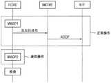
图8是示出根据一些示例实施例的存储系统的操作的顺序图,图9是示出根据一些示例实施例的存储装置的操作时间的示图。图8和图9示出了当在主机装置1100的请求下执行写操作以将数据写入非易失性存储器装置400中时的示例。FIG. 8 is a sequence diagram illustrating operations of a storage system according to some example embodiments, and FIG. 9 is a diagram illustrating operation times of a storage device according to some example embodiments. 8 and 9 illustrate an example when a write operation is performed at the request of the
参照图8和图9,在时间间隔T1至T2中,伴随逻辑地址LA和写数据WDT的数据写请求WRREQ可从主机装置1100传送至存储控制器100。Referring to FIGS. 8 and 9 , a data write request WRREQ accompanied by a logical address LA and write data WDT may be transmitted from the
在时间间隔T2至T3中,存储控制器100可基于第一固件元数据FMDT1执行伴随或导致第一固件元数据FMDT1的变化的第一管理操作MNGOP1(操作S52)。另外,存储控制器100可执行访问操作ACCOP,以将写数据WDT和通过第一管理操作MNGOP1确定的物理地址PA传送至非易失性存储器装置400(操作S53)。然后,非易失性存储器装置400可执行编程操作,以将写数据WDT存储在对应于物理地址PA的存储器区中(操作S54)。During the time interval T2 to T3, the
在时间间隔T3至T4中,存储控制器100可基于第二固件元数据FMDT2执行伴随或导致第二固件元数据FMDT2的变化的第二管理操作MNGOP2(操作S55)。然后,存储控制器100可执行元数据检查,以将第一固件元数据FMDT1的变化和第二固件元数据FMDT2的变化进行比较(操作S56)。In the time interval T3 to T4, the
当存储控制器100确定在元数据中出现了软错误时,存储控制器100可以将错误通知ERRNF传送至主机装置1100(操作S57)。When the
如图9所示,第二管理操作MNGOP2可与访问操作ACCOP和编程操作同时地和/或独立地被执行。通常,非易失性存储器装置400内的编程操作可需要相对长的时间,因此在执行访问操作ACCOP和编程操作的同时,第二管理操作MNGOP2和元数据检查可在时间间隔T3至T4内被充分执行。As shown in FIG. 9 , the second management operation MNGOP2 may be performed simultaneously with and/or independently from the access operation ACCOP and the program operation. Generally, a program operation within the
这样,根据示例实施例的存储装置1200和操作存储装置的方法可有效地和/或在不过分减小存储装置的操作速度的情况下监视元数据中的错误,这是因为非易失性存储器装置可与虚拟操作独立地和/或同时地执行访问操作。As such, the
图10是示出根据一些示例实施例的操作存储装置的方法的流程图。FIG. 10 is a flowchart illustrating a method of operating a storage device according to some example embodiments.
参照图10,可基于存储在非易失性存储器装置中的非易失性元数据生成第一固件元数据、第二固件元数据和第三固件元数据(操作S110)。Referring to FIG. 10 , first, second, and third firmware metadata may be generated based on nonvolatile metadata stored in a nonvolatile memory device (operation S110 ).
可执行正常操作,正常操作包括伴随或导致第一固件元数据的变化的第一管理操作,并且还包括可访问非易失性存储器装置的访问操作(操作S210)。A normal operation including a first management operation accompanying or causing a change of the first firmware metadata and further including an access operation that can access the nonvolatile memory device may be performed (operation S210).
可执行第一虚拟操作,第一虚拟操作包括伴随或导致第二固件元数据的变化的第二管理操作,并且在第一虚拟操作期间,访问操作可受限和/或非易失性存储器装置可不被访问(操作S310)。A first virtual operation may be performed, the first virtual operation includes a second management operation accompanying or causing a change in the second firmware metadata, and during the first virtual operation, access operations may be restricted and/or the non-volatile memory device May not be accessed (operation S310).
可执行附加的虚拟操作或第二虚拟操作,附加的虚拟操作或第二虚拟操作包括伴随或导致第三固件元数据的变化的第三管理操作,并且在第二虚拟操作期间,访问操作可受限和/或非易失性存储器装置可不被访问(操作S320)。An additional virtual operation or a second virtual operation may be performed, the additional virtual operation or the second virtual operation includes a third management operation accompanying or causing a change in the third firmware metadata, and during the second virtual operation, the access operation may be subject to The limited and/or nonvolatile memory device may not be accessed (operation S320).
可通过将由第一管理操作导致的第一固件元数据的变化、由第二管理操作导致的第二固件元数据的变化和由第三管理操作导致的第三固件元数据的变化进行比较来确定在第一固件元数据中是否出现了错误(操作S410)。can be determined by comparing changes in first firmware metadata caused by a first management operation, changes in second firmware metadata caused by a second management operation, and changes in third firmware metadata caused by a third management operation Whether an error occurs in the first firmware metadata (operation S410).
除附加的虚拟操作或第二虚拟操作之外,图10的方法基本上类似于参照图1至图9描述的方法,并且可省略重复描述。Except for an additional dummy operation or a second dummy operation, the method of FIG. 10 is substantially similar to the method described with reference to FIGS. 1 to 9 , and repeated descriptions may be omitted.
图11是示出根据一些示例实施例的由存储控制器管理的固件元数据的示例实施例的示图。FIG. 11 is a diagram illustrating an example embodiment of firmware metadata managed by a storage controller according to some example embodiments.
参照图11,由存储控制器100生成和管理的多个固件元数据301可包括第一固件元数据FMDT1、第二固件元数据FMDT2和第三固件元数据FMDT3。Referring to FIG. 11 , a plurality of
第一固件元数据FMDT1可包括第一日志记录集JLS1、固件映射表FMAP和第一管理数据CMDT1。第一日志记录集JLS1可以存储通过或由第一管理操作导致的第一固件元数据FMDT1的变化。固件映射表FMAT可以存储从主机装置1100提供的逻辑地址和非易失性存储器装置400的物理地址之间的映射关系。第一管理数据CMDT1可包括关于非易失性存储器装置400的坏块、有效页计数等的信息。The first firmware metadata FMDT1 may include a first log record set JLS1, a firmware mapping table FMAP, and first management data CMDT1. The first log record set JLS1 may store changes to the first firmware metadata FMDT1 by or caused by the first management operation. The firmware mapping table FMAT may store a mapping relationship between a logical address provided from the
第二固件元数据FMDT2可包括第二日志记录集JLS2和第二管理数据CMDT2。第二日志记录集JLS2可以存储通过或由第二管理操作导致的第二固件元数据FMDT2的变化。第二管理数据CMDT2可包括关于非易失性存储器装置400的坏块、有效页计数等的信息。The second firmware metadata FMDT2 may include a second log record set JLS2 and second management data CMDT2. The second log record set JLS2 may store changes to the second firmware metadata FMDT2 by or caused by the second management operation. The second management data CMDT2 may include information on bad blocks, valid page counts, and the like of the
第三固件元数据FMDT3可包括第三日志记录集JLS3和第三管理数据CMDT3。第三日志记录集JLS3可以存储通过或由第三管理操作导致的第三固件元数据FMDT3的变化。第三管理数据CMDT3可包括关于非易失性存储器装置400的坏块、有效页计数等的信息。The third firmware metadata FMDT3 may include a third log record set JLS3 and third management data CMDT3. The third log record set JLS3 may store changes to the third firmware metadata FMDT3 by or caused by the third management operation. The third management data CMDT3 may include information on bad blocks of the
在出现元数据的错误之前,或者如果不出现元数据的错误,则第一日志记录集JLS1可保持与第二日志记录集JLS2一致,第二日志记录集JLS2可保持与第三日志记录集JLS3一致。另外,第一管理数据CMDT1可保持与第二管理数据CMDT2一致,第二管理数据CMDT2可保持与第三管理数据CMDT3一致。Before a metadata error occurs, or if no metadata error occurs, the first log record set JLS1 can remain consistent with the second log record set JLS2, and the second log record set JLS2 can remain consistent with the third log record set JLS3 unanimous. In addition, the first management data CMDT1 may remain consistent with the second management data CMDT2, and the second management data CMDT2 may remain consistent with the third management data CMDT3.
如图11所示,第一固件元数据FMDT1可包括固件映射表FMAP,但是第二固件元数据FMDT2和第三固件元数据FMDT3可不包括固件映射表FMAP。固件映射表FMAP的大小与其它元数据的大小相比可能非常大,并且如果存储控制器100要存储多个固件映射表,则存储控制器100的大小和成本可能显著增大。存储控制器100可以在图3中的缓冲器存储器140中存储一个固件映射表FMAP并且可通过参照图7描述的映射表恢复操作执行第一管理操作和第二管理操作。As shown in FIG. 11 , the first firmware metadata FMDT1 may include the firmware mapping table FMAP, but the second firmware metadata FMDT2 and the third firmware metadata FMDT3 may not include the firmware mapping table FMAP. The size of the firmware map FMAP may be very large compared to the size of other metadata, and the size and cost of the
这样,根据一些示例实施例的存储装置和操作存储装置的方法可以更有效地和/或在不过分增大存储控制器中的缓冲器存储器的存储容量的情况下监视元数据中的错误,这是因为仅多个元数据中的一个元数据可包括具有相对更大的大小的固件映射表。As such, storage devices and methods of operating storage devices according to some example embodiments can monitor errors in metadata more efficiently and/or without unduly increasing the storage capacity of buffer memories in storage controllers, which This is because only one of metadata may include a firmware mapping table having a relatively larger size.
图12是示出根据示例实施例的操作存储装置的方法的流程图。FIG. 12 is a flowchart illustrating a method of operating a storage device according to example embodiments.
参照图12,存储控制器100可以从主机装置1100接收请求REQ(操作S10),并且执行对应于请求REQ的第一管理操作MNGOP1和访问操作ACCOP(操作S11、S12)。可基于第一固件元数据FMDT1执行第一管理操作MNGOP1和访问操作ACCOP,并且第一管理操作MNGOP1可以伴随或导致第一固件元数据FMDT1的变化。Referring to FIG. 12 , the
元数据管理器200可基于第一固件元数据FMDT1的变化(例如,基于第一日志记录集JLS1)执行第一映射表恢复操作MTROP1,以将第一固件元数据FMDT1的固件映射表FMAP恢复至先前状态,例如,恢复至在执行第一管理操作MNGOP1之前固件映射表FMAP的状态(操作S13)。The
存储控制器100可基于第二固件元数据FMDT2和通过第一映射表恢复操作MTROP1恢复的固件映射表FMAP执行第二管理操作MNGOP2(操作S14)。The
这样,因为在第一管理操作MNGOP1之后和在第二管理操作MNGOP2之前恢复固件映射表FMAP,所以第一管理操作MNGOP1和第二管理操作MNGOP2可在相同的条件下被执行。因此,如果未出现错误,则第一固件元数据FMDT1的变化可与第二固件元数据FMDT2的变化相同。As such, since the firmware mapping table FMAP is restored after the first management operation MNGOP1 and before the second management operation MNGOP2, the first management operation MNGOP1 and the second management operation MNGOP2 may be performed under the same condition. Therefore, if no error occurs, the change of the first firmware metadata FMDT1 may be the same as the change of the second firmware metadata FMDT2.
元数据检查器220可以将存储第一固件元数据FMDT1的变化的第一日志记录集JLS1和存储第二固件元数据FMDT2的变化的第二日志记录集JLS2进行比较(操作S15)。The
当第一日志记录集JLS1与第二日志记录集JLS2相同时(操作S15:“是”分支),存储控制器100可以确定第一固件元数据FMDT1中未出现错误。在这种情况下,可省略附加的虚拟操作或第二虚拟操作(即,伴随或导致第三固件元数据FMDT3的变化的第三管理操作MNGOP3)。第一固件元数据FMDT1和第二固件元数据FMDT2的一致性可保持,但是第三固件元数据FMDT3相对于第一固件元数据FMDT1和第二固件元数据FMDT2的一致性可不保持,这是因为省略了或未执行附加的虚拟操作。因此,存储控制器100可以代替第三管理操作MNGOP3来更新第三固件元数据FMDT3,使得第三固件元数据FMDT3可与第二固件元数据FMDT2相同(操作S21)。When the first log record set JLS1 is the same as the second log record set JLS2 (operation S15: YES branch), the
当第一日志记录集JLS1与第二日志记录集JLS2不同时(操作S15:“否”分支),元数据管理器200可基于第二固件元数据FMDT2的变化(例如,基于第二日志记录集JLS2)执行第二映射表恢复操作MTROP2,以将第一固件元数据FMDT1的固件映射表FMAP恢复至先前状态,例如,恢复至在执行第二管理操作MNGOP2之前固件映射表FMAP的状态(操作S22)。When the first log record set JLS1 is different from the second log record set JLS2 (operation S15: "No" branch), the
存储控制器100可基于第三固件元数据FMDT3和通过第二映射表恢复操作MTROP2恢复的固件映射表FMAP执行第三管理操作MNGOP3(操作S23)。The
这样,因为在第二管理操作MNGOP2之后和在第三管理操作MNGOP3之前恢复固件映射表FMAP,所以可在相同的条件下执行第一管理操作MNGOP1和第三管理操作MNGOP3。因此,如果未出现错误,则第一固件元数据FMDT1的变化可与第三固件元数据FMDT3的变化相同。As such, since the firmware mapping table FMAP is restored after the second management operation MNGOP2 and before the third management operation MNGOP3, the first management operation MNGOP1 and the third management operation MNGOP3 may be performed under the same condition. Therefore, if no error occurs, the change of the first firmware metadata FMDT1 may be the same as the change of the third firmware metadata FMDT3.
元数据检查器220可以将存储第一固件元数据FMDT1的变化的第一日志记录集JLS1和存储第三固件元数据FMDT3的变化的第三日志记录集JLS3进行比较(操作S24)。The
当第一日志记录集JLS1与第三日志记录集JLS3相同时(操作S24:“是”分支),存储控制器100可以确定第一固件元数据FMDT1中未出现错误,但是在执行第二管理操作MNGOP2时出现错误。在这种情况下,第一固件元数据FMDT1和第三固件元数据FMDT3的一致性可保持,但是第二固件元数据FMDT2相对于第一固件元数据FMDT1和第三固件元数据FMDT3的一致性可不保持,因为执行附加的虚拟操作可指示暂时的问题和/或指向第二固件元数据FMDT2的问题。因此,存储控制器100可以更新随错误改变的第二固件元数据FMDT2,使得第二固件元数据FMDT2可与第三固件元数据FMDT3相同(操作S25)。When the first log record set JLS1 is the same as the third log record set JLS3 (operation S24: "Yes" branch), the
当第一日志记录集JLS1与第三日志记录集JLS3不同时(操作S24:“否”分支),元数据管理器200可以确定第一固件元数据FMDT1中出现了错误。在这种情况下,存储控制器100可以将错误通知传送至主机装置1100(操作S26)。然后,存储控制器100可执行状态恢复操作STROP,以将存储控制器100和非易失性存储器装置400恢复至先前状态,例如,恢复至执行正常操作之前的状态(操作S27)。状态恢复操作STROP可包括丢弃导致错误的第一固件元数据FMDT1、第二固件元数据FMDT2和第三固件元数据FMDT3,然后基于存储在非易失性存储器装置400中的非易失性元数据将第一固件元数据FMDT1、第二固件元数据FMDT2和第三固件元数据FMDT3初始化。另外,状态恢复操作STROP还可包括删除或更换由于存储在非易失性存储器装置400中的用户数据之中或之内的元数据中的软错误而导致的损坏的数据。When the first log record set JLS1 is different from the third log record set JLS3 (operation S24: "NO" branch), the
图13是示出根据示例实施例的存储控制器的框图。FIG. 13 is a block diagram illustrating a memory controller according to example embodiments.
参照图2和图13,存储控制器100a可包括处理器110、主机接口HIF 120、ROM(只读存储器)130、缓冲器存储器BUFF 140、存储器接口MIF 150和电连接存储控制器100a中的组件的内部总线160。2 and 13, the
主机接口120可以通过总线10连接至主机装置1100,并且可在存储控制器100a与主机装置1100之间提供接口。例如,主机接口120可以使用一个或多个接口协议(诸如通用串行总线(USB)协议、多媒体卡(MMC)协议、外围组件互连(PCI)协议、PCI快速(PCI-E)协议、高级技术附件(ATA)协议、串行ATA协议、并行ATA协议、小型计算机小型接口(SCSI)协议、增强型小型磁盘接口(ESDI)协议、集成驱动器电子设备(IDE)协议、移动工业处理器接口(MIPI)协议、通用闪存(UFS)协议等)与存储控制器100a交换数据。The
主机接口120可包括用于控制相对于主机装置1100的传送信号和数据的主机接口控制逻辑HICL。主机接口控制逻辑HICL可包括寄存器HISFR,寄存器HISFR存储用于控制主机接口120的设定值和与主机接口120的当前操作相对应的状态信息。The
存储器接口150可以通过总线20连接至非易失性存储器装置400,并且可在存储控制器100a与非易失性存储器装置400之间提供接口。可利用多个通道CH0至CHm(图13中未示出)来实施总线20。通道CH0至CHm中的每一个可以与非易失性存储器装置400独立地通信。在一些示例实施例中,存储器接口150可为被配置为符合标准协议,诸如Toggle或开放式NAND闪存接口(ONFI)。The
存储器接口150可包括用于控制相对于非易失性存储器装置400的传送信号和数据的存储器接口控制逻辑MICL。存储器接口控制逻辑MICL可包括寄存器MISFR,寄存器MISFR存储用于控制存储器接口150的设定值和与存储器接口150的当前操作相对应的状态信息。The
ROM 130可以存储用于驱动存储控制器100a的代码和数据。缓冲器存储器140可以缓冲和存储从主机装置1100传送的写数据以及从非易失性存储器装置400传送的读数据。用于驱动存储控制器100a的代码和数据可在初始化处理或开机处理期间从ROM 130加载至缓冲器存储器140,和/或存储在非易失性存储器装置400中的元数据可加载至缓冲器存储器140。The
图13示出了在存储控制器100a中可包括ROM 130和缓冲器存储器140,但是本公开的示例实施例不限于此。在一些示例实施例中,ROM 130和/或缓冲器存储器140可布置在存储控制器100a外部。在一些示例实施例中,可利用DRAM(动态随机存取存储器)来实施缓冲器存储器140。FIG. 13 shows that the
处理器110可控制存储控制器100a的整体操作。处理器110可包括用于运行用于控制存储控制器100a的固件的CPU、微处理器等。The
处理器110可包括多个处理器核或者多个控制器。在一些示例实施例中,处理器110可包括主机核HCORE 111、闪存转换层(FTL)核112(FCORE)和NAND管理器(NM)核113(NMCORE)。可以利用不同的处理器核来实施主机核111、FTL核112和NM核113。The
主机核111可以从主机接口120接收请求集。主机核111可以分析请求集,并且将各个请求传送至对应的核。
主机核111可包括操作存储器HOM、奇偶逻辑PRTC和寄存器HSFR。奇偶逻辑PRTC可以生成与用于驱动主机核111的操作代码和操作数据相对应的奇偶校验位,并且可以在操作存储器HOM中与操作代码和操作数据一起存储奇偶校验位。寄存器HSFR可以存储用于控制主机核111的操作的设定值,并且可以存储指示主机核111的当前操作的状态信息。The
FTL核112可基于从主机核111接收的请求REQ控制NM核113,使得可在非易失性存储器装置400中执行操作(诸如读操作、编程操作、擦除操作等)。The
FTL核112可包括操作存储器FOM、奇偶逻辑PRTC和寄存器FSFR。奇偶逻辑PRTC可以生成与用于驱动FTL核112的操作代码和操作数据相对应的奇偶校验位,并且可以在操作存储器FOM中与操作代码和操作数据一起存储奇偶校验位。寄存器FSFR可以存储用于控制FTL核112的操作的设定值,并且可以存储指示FTL核112的当前操作的状态信息。The
NM核113可在FTL核112的控制下控制存储器接口150,使得可执行相对于非易失性存储器装置400的操作。The
NM核113可包括操作存储器NMOM、奇偶逻辑PRTC和寄存器NMSFR。奇偶逻辑PRTC可以生成与用于驱动NM核113的操作代码和操作数据相对应的奇偶校验位,并且可以在操作存储器NMOM中与操作代码和操作数据一起存储奇偶校验位。寄存器NMSFR可以存储用于控制NM核113的操作的设定值,并且可以存储指示NM核113的当前操作的状态信息。The
用于驱动主机核111、FTL核112和NM核113的操作代码和操作数据可在存储控制器100a的初始化处理期间从ROM 130和/或非易失性存储器装置400加载至缓冲器存储器140。主机核111、FTL核112和NM核113中的每一个可从缓冲器存储器140加载操作代码和操作数据的至少一部分,并且可以将加载的代码和数据存储在对应的操作存储器HOM、FOM和NMOM中。在一些示例实施例中,操作代码和操作数据可从ROM 130和/或非易失性存储器装置400直接加载至操作存储器HOM、FOM和NMOM。在一些示例实施例中,可利用SRAM(静态动态随机存取存储器)来实施操作存储器HOM、FOM和NMOM。Operation codes and operation data for driving the
FTL核112可基于通过主机接口120从主机装置1100接收的请求REQ发布将在非易失性存储器装置400中执行的操作,并且NM核113可基于存储在操作存储器NMOM中的操作代码和操作数据控制存储器接口150,使得非易失性存储器装置400可执行从较高等级控制器FCORE接收的发布的操作。在这种情况下,FTL核112对应于等级高于NM核113的处理器核,因此,FTL核112可被称作较高等级控制器FCORE,NM核113可被称作较低等级控制器NMCORE。The
图14是示出根据一些示例实施例的存储控制器的固件的层级结构的示图。FIG. 14 is a diagram illustrating a hierarchical structure of firmware of a memory controller according to some example embodiments.
参照图13和图14,存储控制器100a的固件可包括主机接口层HIL、闪存转换层FTL、虚拟闪存层VFL、闪存接口层FIL、虚拟中断层VIC和NAND管理器(NM)层NML。13 and 14, the firmware of the
当通过主机接口120接收来自主机装置1100的请求时,(可由主机核HCORE执行的)主机接口层HIL可以对请求进行解码,并且将经解码的请求存储在寄存器HISFR中。主机接口层HIL可以通过轮询方案或中断方案接收存储在寄存器HISFR中的信息,并且确定接收的请求是否合适。When a request from the
(由较高等级控制器FCORE执行的)闪存转换层FTL可以将从主机装置1100传送的逻辑块地址(LBA)映射至指示非易失性存储器装置400的物理位置的物理块地址(PBA)。The flash translation layer FTL (executed by the higher-level controller FCORE) may map a logical block address (LBA) transferred from the
(由较低等级控制器NMCORE执行的)NM层NML可控制存储器接口150的操作。由较高等级控制器FCORE执行的虚拟闪存层VFL和闪存接口层FIL可控制较低等级控制器NMCORE的操作。虚拟闪存层VFL可以管理非易失性存储器装置400的坏块信息。(由较高等级控制器FCORE执行的)虚拟中断层VIC可以管理在较低等级控制器NMCORE中出现的异常事件,例如,异常。The NM layer NML (executed by the lower level controller NMCORE) may control the operation of the
参照图15进一步描述根据一些示例实施例的存储控制器100a的固件配置。A firmware configuration of the
图15是示出根据一些示例实施例的存储控制器中包括的较高等级控制器和较低等级控制器的固件配置的示例实施例的示图。FIG. 15 is a diagram illustrating an example embodiment of a firmware configuration of a higher-level controller and a lower-level controller included in a memory controller according to some example embodiments.
参照图13、图14和图15,较低等级控制器NMCORE的NM层NML可包括操作代码OCD、操作数据ODT、以及包括可从较高等级控制器FCORE发布的发布的操作OP1至OP4的发布的队列列表IQLST。较低等级控制器NMCORE可以在较低等级控制器NMCORE的操作存储器NMOM中存储操作代码OCD和操作数据ODT,并且可以执行存储的操作代码OCD。可以通过更新作为初始加载的数据的操作数据ODT的一部分将发布的队列列表IQLST存储在操作存储器NMOM中。Referring to Figures 13, 14 and 15, the NM layer NML of the lower level controller NMCORE may include Operation Code OCD, Operation Data ODT, and Issues of Operations OP1 to OP4 including Issues that may be issued from the higher level controller FCORE The queue list IQLST. The lower-level controller NMCORE may store the operation code OCD and the operation data ODT in the operation memory NMOM of the lower-level controller NMCORE, and may execute the stored operation code OCD. The issued queue list IQLST can be stored in the operational memory NMOM by updating a part of the operational data ODT which is initially loaded data.
较高等级控制器FCORE的虚拟闪存层VFL可包括输入-输出队列IOQ。输入-输出队列IOQ可包括等待队列WTQ、取消队列CNQ和错误队列ERQ。较高等级控制器FCORE可以将输入-输出队列IOQ存储在较高等级控制器FCORE的操作存储器FOM和/或缓冲器存储器140中。The virtual flash layer VFL of the higher-level controller FCORE may include input-output queues IOQ. Input-output queues IOQ may include wait queues WTQ, cancel queues CNQ, and error queues ERQ. The higher-level controller FCORE may store the input-output queue IOQ in the operational memory FOM and/or
等待队列WTQ可包括待传送至较低等级控制器NMCORE的等待操作。取消队列CNQ可包括从闪存接口层FIL返回的操作。错误队列ERQ可包括涉及非易失性存储器装置400的坏块的操作。根据一些示例实施例,等待队列WTQ和取消队列CNQ可组合为一个队列(未示出)。The waiting queue WTQ may comprise waiting operations to be transferred to the lower level controller NMCORE. Cancel queue CNQ may include operations returning from the flash interface layer FIL. The error queue ERQ may include operations involving bad blocks of the
较高等级控制器FCORE的虚拟中断层VIC可包括中断处理器INTRH。在一些示例实施例中,较高等级控制器FCORE可以在较高等级控制器FCORE的操作存储器FOM中存储对应于中断处理器INTRH的操作代码和操作数据,并且可以执行存储的操作代码。在一些示例实施例中,中断处理器INTRH可被实施为与较高等级控制器FCORE不同的硬件或包括在较高等级控制器FCORE中的硬件。The virtual interrupt layer VIC of the higher-level controller FCORE may include an interrupt handler INTRH. In some example embodiments, the higher-level controller FCORE may store operation codes and operation data corresponding to the interrupt handler INTRH in an operation memory FOM of the higher-level controller FCORE, and may execute the stored operation codes. In some example embodiments, the interrupt handler INTRH may be implemented as hardware different from or included in the higher-level controller FCORE.
较高等级控制器FCORE的闪存接口层FIL可包括恢复处理器RCVH和通信队列CMQ。较高等级控制器FCORE可以在较高等级控制器FCORE的操作存储器FOM中存储对应于恢复处理器RCVH的操作代码和操作数据,并且可以执行存储的操作代码。较高等级控制器FCORE可以在较高等级控制器FCORE的操作存储器FOM和/或缓冲器存储器140中存储通信队列CMQ。The flash interface layer FIL of the higher-level controller FCORE may include a recovery processor RCVH and a communication queue CMQ. The higher-level controller FCORE may store operation codes and operation data corresponding to the recovery processor RCVH in the operation memory FOM of the higher-level controller FCORE, and may execute the stored operation codes. The higher-level controller FCORE may store the communication queue CMQ in the operational memory FOM and/or
通信队列CMQ可包括关于传送至较低等级控制器NMCORE的发布的操作的发布信息。如上所述,非易失性存储器装置400可以通过可独立地通信的多个通道CH0至CHm连接至存储器接口150。在这种情况下,通信队列CMQ可包括分别存储与多个通道CH0至CHm相对应的发布信息的多个子队列0CHQ至mCHQ。The communication queue CMQ may contain publication information about the operation of publications transmitted to the lower level controller NMCORE. As described above, the
中断处理器INTRH可以响应于较低等级控制器NMCORE中的中断停止较低等级控制器NMCORE和存储器接口150的操作。恢复控制器RCVH可以将较低等级控制器NMCORE和存储器接口150的状态信息备份。恢复处理器RCVH可以基于备份信息恢复较低等级控制器NMCORE和存储器接口150的状态。The interrupt handler INTRH may stop the operations of the lower-level controller NMCORE and the
较高等级控制器FCORE的闪存转换层FTL可包括操作代码OCD、操作数据ODT、元数据管理器MDMNG和多个固件元数据FMDT1至FMDT3。较高等级控制器FCORE可以在较高等级控制器FCORE的操作存储器FOM中存储操作代码OCD和操作数据ODT,并且可以执行存储的操作代码OCD。另外,较高等级控制器FCORE可以在缓冲器存储器140中存储多个固件元数据FMDT1至FMDT3。The flash translation layer FTL of the higher-level controller FCORE may include an operation code OCD, an operation data ODT, a metadata manager MDMNG, and a plurality of firmware metadata FMDT1 to FMDT3. The higher-level controller FCORE can store the operation code OCD and the operation data ODT in the operation memory FOM of the higher-level controller FCORE, and can execute the stored operation code OCD. In addition, the higher-level controller FCORE may store a plurality of firmware metadata FMDT1 to FMDT3 in the
图16是示出根据一些示例实施例的存储系统的操作的顺序图。FIG. 16 is a sequence diagram illustrating operations of a storage system according to some example embodiments.
参照图16,较高等级控制器FCORE可执行伴随第一固件元数据FMDT1的变化的第一管理操作MNGOP1,并且可以将根据第一管理操作MNGOP1生成的发布的操作传送至较低等级控制器NMCORE。较低等级控制器NMCORE可执行访问操作ACCOP,以基于发布的操作控制存储器接口MIF。这样,存储控制器100或100a可执行包括第一管理操作MNGOP1和访问操作ACCOP的正常操作。Referring to FIG. 16 , the higher-level controller FCORE may execute the first management operation MNGOP1 accompanying the change of the first firmware metadata FMDT1, and may transfer the published operations generated according to the first management operation MNGOP1 to the lower-level controller NMCORE . The lower level controller NMCORE can execute the access operation ACCOP to control the memory interface MIF based on the issued operation. As such, the
另外,较高等级控制器FCORE可执行包括伴随第二固件元数据FMDT2的变化的第二管理操作MNGOP2的虚拟操作。在这种情况下,较高等级控制器FCORE可不生成发布的操作,因此较低等级控制器NMCORE可不执行访问操作ACCOP。In addition, the higher-level controller FCORE may perform a virtual operation including a second management operation MNGOP2 accompanied by a change of the second firmware metadata FMDT2. In this case, the higher-level controller FCORE may not generate the issued operation, so the lower-level controller NMCORE may not execute the access operation ACCOP.
然后,较高等级控制器FCORE可通过将第一固件元数据FMDT1的变化和第二固件元数据FMDT2的变化进行比较来执行元数据检查以确定是否出现软错误。Then, the higher-level controller FCORE may perform a metadata check to determine whether a soft error occurs by comparing changes in the first firmware metadata FMDT1 and changes in the second firmware metadata FMDT2.
这样,较高等级控制器FCORE可以仅在正常操作期间将发布的操作传送至较低等级控制器NMCORE,使得在虚拟操作期间可不执行访问操作ACCOP。In this way, the higher-level controller FCORE can transfer issued operations to the lower-level controller NMCORE only during normal operation, so that the access operation ACCOP may not be performed during virtual operations.
图17是示出根据一些示例实施例的存储装置中包括的非易失性存储器装置的框图。FIG. 17 is a block diagram illustrating a nonvolatile memory device included in a memory device according to some example embodiments.
参照图17,非易失性存储器装置800可包括存储器单元阵列500、页缓冲器电路510、数据输入/输出(I//O)电路520、地址解码器530、控制电路550和电压生成器560。在一些示例实施例中,非易失性存储器装置800可具有存储器单元阵列布置在外围电路上的外围上单元(COP)结构。在这种情况下,存储器单元阵列500可形成在单元区CREG中,并且页缓冲器电路510、数据I/O电路520、地址解码器530、控制电路550和电压生成器560可形成在外围区PREG中。Referring to FIG. 17, a
存储器单元阵列500可通过串选择线SSL、字线WL和地选择线GSL耦接至地址解码器530。存储器单元阵列500可通过位线BL耦接页缓冲器电路510。存储器单元阵列500可包括耦接至字线WL和位线BL的存储器单元。在一些示例实施例中,存储器单元阵列500可以是可按照三维结构(或竖直结构)形成在衬底上的三维存储器单元阵列。在这种情况下,存储器单元阵列500可包括竖直取向的单元串(例如,NAND串),使得至少一个存储器单元位于另一存储器单元上方。The
控制电路550可以从存储器控制器接收命令信号CMD和地址信号ADDR,并且可响应于(或者基于)命令信号CMD和地址信号ADDR中的至少一个控制非易失性存储器装置800的擦除操作、编程操作和读操作。擦除操作可包括执行一系列擦除循环,编程操作可包括执行一系列编程循环。每个编程循环可包括编程操作和编程验证操作。每个擦除循环可包括擦除操作和擦除验证操作。读操作可包括正常读操作和数据恢复读操作。The
在一些示例实施例中,控制电路550可以生成用于控制电压生成器560的操作的控制信号CTL,并且可以基于命令信号CMD生成用于控制页缓冲器电路510的页缓冲器控制信号PBC,并且可以基于地址信号ADDR生成行地址R_ADDR和列地址C_ADDR。控制电路550可将行地址R_ADDR提供至地址解码器530,并且可将列地址C_ADDR提供至数据I/O电路520。In some example embodiments, the
地址解码器530可通过串选择线SSL、字线WL和地选择线GSL耦接至存储器单元阵列500。在编程操作或读操作期间,地址解码器530可以基于行地址R_ADDR,将字线WL之一确定(或者选择)为所选字线,并且将除所选字线之外的其余字线WL确定或指定为未选字线。The
另外,在编程操作或读操作期间,地址解码器530可以基于行地址R_ADDR,将串选择线SSL之一确定为所选串选择线,并且将除所选串选择线之外的其余串选择线SSL确定或指定为未选串选择线。Also, during a program operation or a read operation, the
电压生成器560可以基于控制信号CTL生成用于非易失性存储器装置800的存储器单元阵列500的操作的字线电压VWL。电压生成器560可以从存储器控制器接收电力PWR。字线电压VWL可通过地址解码器530被施加至字线WL。The
在一些示例实施例中,在擦除操作期间,电压生成器560可以将擦除电压施加至存储器块的阱和/或公共源极线,并且可以基于擦除地址将擦除允许电压(例如,地电压)施加至存储器块的所有字线或者一部分字线。在擦除验证操作期间,电压生成器560可以将擦除验证电压同时地施加至存储器块的所有字线,或者顺序地(例如,一个接一个地)施加至各字线。In some example embodiments, during an erase operation, the
在一些示例实施例中,在编程操作期间,电压生成器560可以将编程电压施加至所选字线,并且可以将编程通过电压施加至未选字线。在编程验证操作期间,电压生成器560可以将编程验证电压施加至所选字线,并且可以将验证通过电压施加至未选字线。In some example embodiments, the
在正常读操作期间,电压生成器560可以将读电压施加至所选字线,并且可以将读通过电压施加至未选字线。在数据恢复读操作期间,电压生成器560可以将读电压施加至邻近于所选字线的字线,并且可以将恢复读电压施加至所选字线。During a normal read operation, the
页缓冲器电路510可通过位线BL耦接至存储器单元阵列500。页缓冲器电路510可包括多个缓冲器。在一些示例实施例中,每个缓冲器可仅连接至一条单独的位线。在一些示例实施例中,每个缓冲器可连接至两条或更多条位线。页缓冲器电路510可以临时存储将被编程在所选页中的数据,或者从存储器单元阵列500的所选页读出的数据。The
数据I/O电路520可通过数据线DL耦接至页缓冲器电路510。在编程操作期间,数据I/O电路520可以接收从存储器控制器接收的编程数据DATA,并且可以基于从控制电路550接收的列地址C_ADDR将编程数据DATA提供至页缓冲器电路510。在读操作期间,数据I/O电路520可基于从控制电路550接收的列地址C_ADDR将已经从存储器单元阵列500读取并且被存储在页缓冲器电路510中的读数据DATA提供至存储器控制器。The data I/
页缓冲器电路510和数据I/O电路520可从存储器单元阵列500的第一区域读取数据,并且可以(例如,在不将数据发送至非易失性存储器装置800外部的源(诸如发送至存储器控制器)的情况下)将该读取的数据写至存储器单元阵列500的第二区域。因此,页缓冲器电路510和数据I/O电路520可执行写回操作。
图18是示出图17的非易失性存储器装置中包括的存储器单元阵列的框图,图19是示出图18的存储器单元阵列中包括的存储器块的等效电路的电路图。18 is a block diagram showing a memory cell array included in the nonvolatile memory device of FIG. 17 , and FIG. 19 is a circuit diagram showing an equivalent circuit of a memory block included in the memory cell array of FIG. 18 .
参照图18,存储器单元阵列500可包括存储器块BLK1至BLKz。在一些示例实施例中,可通过图17的地址解码器530选择存储器块BLK1至BLKz。例如,地址解码器530可以选择存储器块BLK1至BLKz中的对应于块地址的特定存储器块BLK。Referring to FIG. 18 , a
图19的存储器块BLKi可按照三维结构(或竖直结构)形成在衬底上。例如,可以在垂直于衬底的上表面的竖直方向D3上形成存储器块BLKi中包括的NAND串或单元串。The memory block BLKi of FIG. 19 may be formed on the substrate in a three-dimensional structure (or vertical structure). For example, NAND strings or cell strings included in the memory block BLKi may be formed in a vertical direction D3 perpendicular to the upper surface of the substrate.
参照图19,存储器块BLKi可包括耦接在位线BL1、BL2和BL3与公共源极线CSL之间的NAND串NS11至NS33。NAND串NS11至NS33中的每一个可包括串选择晶体管SST、存储器单元MC1至MC8和地选择晶体管GST。在图19中,NAND串NS11至NS33中的每一个被示出为包括八个存储器单元MC1至MC8。然而,示例实施例不限于此,NAND串NS11至NS33中的每一个可包括各种数量的存储器单元。Referring to FIG. 19 , a memory block BLKi may include NAND strings NS11 to NS33 coupled between bit lines BL1 , BL2 , and BL3 and a common source line CSL. Each of the NAND strings NS11 to NS33 may include a string selection transistor SST, memory cells MC1 to MC8 and a ground selection transistor GST. In FIG. 19 , each of the NAND strings NS11 to NS33 is shown to include eight memory cells MC1 to MC8 . However, example embodiments are not limited thereto, and each of the NAND strings NS11 to NS33 may include various numbers of memory cells.
每个串选择晶体管SST可以连接至对应的串选择线(SSL1至SSL3之一)。存储器单元MC1至MC8可以分别连接至对应的栅极线GTL1至GTL8。栅极线GTL1至GTL8可为字线,并且栅极线GTL1至GTL8中的一些可为伪字线。每个地选择晶体管GST可以连接至对应的地选择线(GSL1至GSL3之一)。每个串选择晶体管SST可以连接至对应的位线(例如,BL1、BL2和BL3之一),并且每个地选择晶体管GST可以连接至公共源极线CSL。Each string selection transistor SST may be connected to a corresponding string selection line (one of SSL1 to SSL3). The memory cells MC1 to MC8 may be connected to corresponding gate lines GTL1 to GTL8, respectively. The gate lines GTL1 to GTL8 may be word lines, and some of the gate lines GTL1 to GTL8 may be dummy word lines. Each ground selection transistor GST may be connected to a corresponding ground selection line (one of GSL1 to GSL3 ). Each string selection transistor SST may be connected to a corresponding bit line (eg, one of BL1 , BL2 , and BL3 ), and each ground selection transistor GST may be connected to a common source line CSL.
具有相同或相似高度的字线(例如,WL1)可共同连接,并且地选择线GSL1至GSL3和串选择线SSL1至SSL3可分离。在图19中,存储器块BLKi被示出为耦接至八条栅极线GTL1至GTL8和三条位线BL1至BL3。然而,示例实施例不限于此,并且存储器单元阵列500中的每个存储器块可耦接至各种数量的字线和各种数量的位线。Word lines (eg, WL1 ) having the same or similar height may be commonly connected, and ground selection lines GSL1 to GSL3 and string selection lines SSL1 to SSL3 may be separated. In FIG. 19 , the memory block BLKi is shown coupled to eight gate lines GTL1 to GTL8 and three bit lines BL1 to BL3 . However, example embodiments are not limited thereto, and each memory block in the
图20是示出根据示例实施例的电子装置的框图。FIG. 20 is a block diagram illustrating an electronic device according to example embodiments.
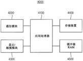
参照图20,电子装置4000可包括应用处理器4100、通信模块4200、显示/触摸模块4300、存储装置4400和缓冲器RAM 4500。Referring to FIG. 20 , the
应用处理器4100可控制电子装置4000的操作。The
通信模块4200可被实施为执行与外部装置的无线或有线通信。The
显示/触摸模块4300可被实施为显示由应用处理器4100处理的数据,或者通过触摸面板接收数据。The display/
存储装置4400可被实施为存储用户数据。存储装置4400可为固态驱动器(SSD)、嵌入式多媒体卡(eMMC)、通用闪存(UFS)等。如上所述,存储装置4400可以存储多个固件元数据并且通过多个管理操作监视元数据的软错误,多个管理操作中的至少一些排除了相应执行访问操作。The
缓冲器RAM 4500可以临时存储用于处理电子装置4000的操作的数据。例如,缓冲器RAM可为诸如DDR(双数据率)SDRAM(同步DRAM)、GDDR(图形DDR)DRAM、RDRAM(RambusDRAM)等的动态随机存取存储器(DRAM)。The
如上所述,存储装置和操作存储装置的方法可以通过冗余地执行伴随或导致元数据的变化的管理操作而不执行对非易失性存储器装置的访问操作,来有效地监视元数据中的错误。As described above, a storage device and a method of operating a storage device can effectively monitor metadata in metadata by redundantly performing management operations that accompany or cause changes in metadata without performing access operations to nonvolatile memory devices. mistake.
可以有效地或更有效地和/或在不过分增大缓冲器存储器的存储容量的情况下监视元数据中的错误,因为仅多个元数据中的一个元数据可包括可具有相对大的大小的固件映射表。Metadata can be monitored for errors efficiently or more efficiently and/or without unduly increasing the storage capacity of the buffer memory, since only one of the plurality of metadata can include firmware mapping table.
另外,可以有效地或更有效地和/或在不过分减小存储装置的操作速度的情况下监视元数据中的错误,因为非易失性存储器装置可与虚拟操作独立地执行访问操作。Additionally, errors in metadata can be monitored efficiently or more efficiently and/or without unduly reducing the operating speed of the storage device because the non-volatile memory device can perform access operations independently of virtual operations.
一些示例实施例可被实施为系统、方法、计算机程序产品或包含一个或多个计算机可读(例如,有形的)介质(在该计算机可读介质上体现有计算机可读程序代码)中的计算机程序产品。计算机可读程序代码可以提供给通用计算机、专用计算机或其他可编程数据处理设备的处理器。计算机可读介质可以是计算机可读信号介质或计算机可读存储介质。计算机可读存储介质可以是任何有形介质,其可以包含或存储供指令执行系统、设备或装置使用或与之结合使用的程序。Some example embodiments may be implemented as a system, method, computer program product, or computer embodying one or more computer-readable (e.g., tangible) media on which computer-readable program code is embodied. program product. Computer readable program code can be provided to a processor of a general purpose computer, special purpose computer, or other programmable data processing apparatus. The computer readable medium may be a computer readable signal medium or a computer readable storage medium. A computer readable storage medium may be any tangible medium that can contain or store the program for use by or in connection with the instruction execution system, apparatus, or apparatus.
实施例可应用于各种电子装置和系统。例如,实施例可应用于诸如存储卡、固态驱动器(SSD)、嵌入式多媒体卡(eMMC)、通用闪存(UFS)、移动电话、智能电话、个人数字助理(PDA)、便携式多媒体播放器(PMP)、数码相机、摄像机、个人计算机(PC)、服务器计算机、工作站、笔记本计算机、数字TV、机顶盒、便携式游戏机、导航系统、可穿戴装置、物联网(IoT)装置、万物网(IoE)装置、电子书、虚拟现实(VR)装置、服务器系统、汽车驾驶系统等的系统。Embodiments are applicable to various electronic devices and systems. For example, embodiments are applicable to devices such as memory cards, solid state drives (SSD), embedded multimedia cards (eMMC), universal flash memory (UFS), mobile phones, smartphones, personal digital assistants (PDAs), portable multimedia players (PMP ), digital cameras, video cameras, personal computers (PCs), server computers, workstations, notebook computers, digital TVs, set-top boxes, portable game consoles, navigation systems, wearable devices, Internet of Things (IoT) devices, Internet of Everything (IoE) devices , e-books, virtual reality (VR) devices, server systems, car driving systems, etc.
上述内容是一些示例实施例的说明,对这些示例实施例的描述不应被解释为对本文所公开的本发明构思的限制。尽管已经描述了一些示例实施例,但本领域技术人员将容易理解,在不实质上脱离本发明构思的情况下,在示例实施例中可以进行许多修改。The foregoing is a description of some example embodiments, and the description of these example embodiments should not be construed as limitations on the inventive concepts disclosed herein. Although a few example embodiments have been described, those skilled in the art will readily appreciate that many modifications are possible in the example embodiments without materially departing from the inventive concept.
Claims (20)
Translated fromChineseApplications Claiming Priority (2)
| Application Number | Priority Date | Filing Date | Title |
|---|---|---|---|
| KR10-2021-0054233 | 2021-04-27 | ||
| KR1020210054233AKR20220147292A (en) | 2021-04-27 | 2021-04-27 | Storage device of performing meta data management and method of operating the same |
Publications (1)
| Publication Number | Publication Date |
|---|---|
| CN115248748Atrue CN115248748A (en) | 2022-10-28 |
Family
ID=83695171
Family Applications (1)
| Application Number | Title | Priority Date | Filing Date |
|---|---|---|---|
| CN202210441483.3APendingCN115248748A (en) | 2021-04-27 | 2022-04-25 | Storage device performing metadata management and method of operating the same |
Country Status (3)
| Country | Link |
|---|---|
| US (1) | US11829228B2 (en) |
| KR (1) | KR20220147292A (en) |
| CN (1) | CN115248748A (en) |
Family Cites Families (14)
| Publication number | Priority date | Publication date | Assignee | Title |
|---|---|---|---|---|
| US6298425B1 (en)* | 1999-01-12 | 2001-10-02 | Compaq Computer Corp. | Computer disk management system using doublet A-B logging |
| US6718494B1 (en) | 2000-12-22 | 2004-04-06 | Intel Corporation | Method and apparatus for preventing and recovering from TLB corruption by soft error |
| US8762620B2 (en) | 2007-12-27 | 2014-06-24 | Sandisk Enterprise Ip Llc | Multiprocessor storage controller |
| US20110040924A1 (en) | 2009-08-11 | 2011-02-17 | Selinger Robert D | Controller and Method for Detecting a Transmission Error Over a NAND Interface Using Error Detection Code |
| US8572311B1 (en) | 2010-01-11 | 2013-10-29 | Apple Inc. | Redundant data storage in multi-die memory systems |
| US8954647B2 (en)* | 2011-01-28 | 2015-02-10 | Apple Inc. | Systems and methods for redundantly storing metadata for non-volatile memory |
| US8700951B1 (en) | 2011-03-09 | 2014-04-15 | Western Digital Technologies, Inc. | System and method for improving a data redundancy scheme in a solid state subsystem with additional metadata |
| US8954694B2 (en) | 2012-11-15 | 2015-02-10 | Western Digital Technologies, Inc. | Methods, data storage devices and systems for fragmented firmware table rebuild in a solid state drive |
| US9384088B1 (en) | 2014-02-24 | 2016-07-05 | Western Digital Technologies, Inc. | Double writing map table entries in a data storage system to guard against silent corruption |
| US10162537B2 (en) | 2015-09-10 | 2018-12-25 | Samsung Electronics Co., Ltd. | Methods and systems to detect silent corruption of data |
| US10275308B2 (en) | 2016-02-24 | 2019-04-30 | Maxta, Inc. | Detecting and correcting silent data corruption in a distributed storage system |
| KR20210029384A (en)* | 2019-09-06 | 2021-03-16 | 에스케이하이닉스 주식회사 | Memory controller and operating method thereof |
| KR20220005832A (en)* | 2020-07-07 | 2022-01-14 | 에스케이하이닉스 주식회사 | Apparatus and method for managing meta data |
| US11467970B1 (en)* | 2021-08-03 | 2022-10-11 | Kioxia Corporation | Metadata management in non-volatile memory devices using in-memory journal |
- 2021
- 2021-04-27KRKR1020210054233Apatent/KR20220147292A/enactivePending
- 2021-12-08USUS17/545,578patent/US11829228B2/enactiveActive
- 2022
- 2022-04-25CNCN202210441483.3Apatent/CN115248748A/enactivePending
Also Published As
| Publication number | Publication date |
|---|---|
| US20220342744A1 (en) | 2022-10-27 |
| US11829228B2 (en) | 2023-11-28 |
| KR20220147292A (en) | 2022-11-03 |
Similar Documents
| Publication | Publication Date | Title |
|---|---|---|
| CN107766257B (en) | Memory system and method of operation | |
| CN110473582B (en) | Memory system and method of operation thereof | |
| KR102564774B1 (en) | Apparatus for diagnosing memory system or data processing system and operating method of memory system or data processing system based on diagnosis | |
| CN109390003B (en) | Memory system and method of operation thereof | |
| CN108694017A (en) | Storage system and its operating method | |
| US11204846B2 (en) | Memory system and method for operating the same | |
| CN107450845B (en) | Memory system and method of operation | |
| CN111400200A (en) | Controller and operation method thereof | |
| CN110765029B (en) | Controller and method for operating the same | |
| CN110968522B (en) | Memory system and method of operation thereof, database system including memory system | |
| CN110727398B (en) | Memory system and operating method thereof | |
| KR102653389B1 (en) | Memory system and operating method of memory system | |
| CN110457230A (en) | Memory system and method of operation | |
| CN108241470B (en) | Controller and its method of operation | |
| CN108427536B (en) | Memory system and method of operating the same | |
| CN110197695B (en) | Memory system and operating method thereof | |
| US12189464B2 (en) | Method of managing debugging log in storage device | |
| CN110910941B (en) | Memory system and operating method thereof | |
| CN111755061A (en) | Apparatus and method for checking the operational status of a memory device in a memory system | |
| CN108932202A (en) | Storage system and its operating method | |
| CN110196816B (en) | Controller, method of operating the same, and memory system including the controller | |
| CN109521946B (en) | Data processing system and method of operation | |
| CN110556153B (en) | Memory device and operation method thereof | |
| KR20190046169A (en) | Data processing system and operating method thereof | |
| US20190026222A1 (en) | Controller and operation method thereof |
Legal Events
| Date | Code | Title | Description |
|---|---|---|---|
| PB01 | Publication | ||
| PB01 | Publication | ||
| SE01 | Entry into force of request for substantive examination | ||
| SE01 | Entry into force of request for substantive examination |