CN115231509A - Wafer level vacuum packaging cavity and packaging method of sandwich type micro-electromechanical system - Google Patents
Wafer level vacuum packaging cavity and packaging method of sandwich type micro-electromechanical systemDownload PDFInfo
- Publication number
- CN115231509A CN115231509ACN202210800894.7ACN202210800894ACN115231509ACN 115231509 ACN115231509 ACN 115231509ACN 202210800894 ACN202210800894 ACN 202210800894ACN 115231509 ACN115231509 ACN 115231509A
- Authority
- CN
- China
- Prior art keywords
- packaging
- layer
- bonding
- cavity
- ring
- Prior art date
- Legal status (The legal status is an assumption and is not a legal conclusion. Google has not performed a legal analysis and makes no representation as to the accuracy of the status listed.)
- Granted
Links
- 238000004806packaging method and processMethods0.000titleclaimsabstractdescription82
- 238000000034methodMethods0.000titleclaimsabstractdescription56
- 238000009461vacuum packagingMethods0.000titleclaimsabstractdescription34
- 230000008569processEffects0.000claimsdescription24
- 238000005538encapsulationMethods0.000claimsdescription22
- 238000000151depositionMethods0.000claimsdescription16
- 229910052710siliconInorganic materials0.000claimsdescription16
- 239000010703siliconSubstances0.000claimsdescription16
- XUIMIQQOPSSXEZ-UHFFFAOYSA-NSiliconChemical compound[Si]XUIMIQQOPSSXEZ-UHFFFAOYSA-N0.000claimsdescription15
- 230000000694effectsEffects0.000claimsdescription14
- 238000001755magnetron sputter depositionMethods0.000claimsdescription12
- 230000008021depositionEffects0.000claimsdescription11
- 238000001312dry etchingMethods0.000claimsdescription5
- 238000001039wet etchingMethods0.000claimsdescription5
- 239000000463materialSubstances0.000claimsdescription3
- 239000000758substrateSubstances0.000claimsdescription3
- HBMJWWWQQXIZIP-UHFFFAOYSA-Nsilicon carbideChemical compound[Si+]#[C-]HBMJWWWQQXIZIP-UHFFFAOYSA-N0.000claimsdescription2
- 229910010271silicon carbideInorganic materials0.000claimsdescription2
- 239000010410layerSubstances0.000abstractdescription111
- 238000013461designMethods0.000abstractdescription12
- 238000005516engineering processMethods0.000abstractdescription8
- 238000012858packaging processMethods0.000abstractdescription3
- 238000004891communicationMethods0.000abstract1
- 239000002356single layerSubstances0.000abstract1
- 235000012431wafersNutrition0.000description23
- 239000007789gasSubstances0.000description19
- 239000010931goldSubstances0.000description10
- 238000010894electron beam technologyMethods0.000description9
- 238000002207thermal evaporationMethods0.000description9
- 238000005530etchingMethods0.000description7
- 238000001459lithographyMethods0.000description7
- 238000004377microelectronicMethods0.000description6
- 238000011161developmentMethods0.000description5
- 238000010586diagramMethods0.000description5
- 230000004913activationEffects0.000description4
- 238000000206photolithographyMethods0.000description4
- SBEQWOXEGHQIMW-UHFFFAOYSA-NsiliconChemical compound[Si].[Si]SBEQWOXEGHQIMW-UHFFFAOYSA-N0.000description4
- 238000001179sorption measurementMethods0.000description4
- 230000008901benefitEffects0.000description3
- 229920002120photoresistant polymerPolymers0.000description3
- 238000004544sputter depositionMethods0.000description3
- XLYOFNOQVPJJNP-UHFFFAOYSA-NwaterChemical compoundOXLYOFNOQVPJJNP-UHFFFAOYSA-N0.000description3
- 230000008859changeEffects0.000description2
- 238000009792diffusion processMethods0.000description2
- ALKZAGKDWUSJED-UHFFFAOYSA-Ndinuclear copper ionChemical compound[Cu].[Cu]ALKZAGKDWUSJED-UHFFFAOYSA-N0.000description2
- QUCZBHXJAUTYHE-UHFFFAOYSA-NgoldChemical compound[Au].[Au]QUCZBHXJAUTYHE-UHFFFAOYSA-N0.000description2
- 238000010438heat treatmentMethods0.000description2
- 238000004519manufacturing processMethods0.000description2
- 230000003647oxidationEffects0.000description2
- 238000007254oxidation reactionMethods0.000description2
- 238000012536packaging technologyMethods0.000description2
- 230000000630rising effectEffects0.000description2
- 208000032750Device leakageDiseases0.000description1
- UFHFLCQGNIYNRP-UHFFFAOYSA-NHydrogenChemical compound[H][H]UFHFLCQGNIYNRP-UHFFFAOYSA-N0.000description1
- 239000000443aerosolSubstances0.000description1
- QVGXLLKOCUKJST-UHFFFAOYSA-Natomic oxygenChemical compound[O]QVGXLLKOCUKJST-UHFFFAOYSA-N0.000description1
- 230000009286beneficial effectEffects0.000description1
- 239000003795chemical substances by applicationSubstances0.000description1
- 230000007547defectEffects0.000description1
- 230000003111delayed effectEffects0.000description1
- 230000005496eutecticsEffects0.000description1
- 239000011521glassSubstances0.000description1
- 239000001257hydrogenSubstances0.000description1
- 229910052739hydrogenInorganic materials0.000description1
- 239000011229interlayerSubstances0.000description1
- 230000007774longtermEffects0.000description1
- 238000012423maintenanceMethods0.000description1
- 238000012986modificationMethods0.000description1
- 230000004048modificationEffects0.000description1
- 239000001301oxygenSubstances0.000description1
- 229910052760oxygenInorganic materials0.000description1
- 230000035515penetrationEffects0.000description1
- 238000011160researchMethods0.000description1
- 239000004065semiconductorSubstances0.000description1
- 239000002210silicon-based materialSubstances0.000description1
- 239000000126substanceSubstances0.000description1
- 230000003746surface roughnessEffects0.000description1
- 230000007704transitionEffects0.000description1
Images


Classifications
- B—PERFORMING OPERATIONS; TRANSPORTING
- B81—MICROSTRUCTURAL TECHNOLOGY
- B81B—MICROSTRUCTURAL DEVICES OR SYSTEMS, e.g. MICROMECHANICAL DEVICES
- B81B7/00—Microstructural systems; Auxiliary parts of microstructural devices or systems
- B81B7/0032—Packages or encapsulation
- B81B7/0035—Packages or encapsulation for maintaining a controlled atmosphere inside of the chamber containing the MEMS
- B81B7/0038—Packages or encapsulation for maintaining a controlled atmosphere inside of the chamber containing the MEMS using materials for controlling the level of pressure, contaminants or moisture inside of the package, e.g. getters
- B—PERFORMING OPERATIONS; TRANSPORTING
- B81—MICROSTRUCTURAL TECHNOLOGY
- B81B—MICROSTRUCTURAL DEVICES OR SYSTEMS, e.g. MICROMECHANICAL DEVICES
- B81B7/00—Microstructural systems; Auxiliary parts of microstructural devices or systems
- B81B7/0032—Packages or encapsulation
- B81B7/0045—Packages or encapsulation for reducing stress inside of the package structure
- B—PERFORMING OPERATIONS; TRANSPORTING
- B81—MICROSTRUCTURAL TECHNOLOGY
- B81C—PROCESSES OR APPARATUS SPECIALLY ADAPTED FOR THE MANUFACTURE OR TREATMENT OF MICROSTRUCTURAL DEVICES OR SYSTEMS
- B81C1/00—Manufacture or treatment of devices or systems in or on a substrate
- B81C1/00015—Manufacture or treatment of devices or systems in or on a substrate for manufacturing microsystems
- B81C1/00261—Processes for packaging MEMS devices
- B81C1/00277—Processes for packaging MEMS devices for maintaining a controlled atmosphere inside of the cavity containing the MEMS
- B81C1/00285—Processes for packaging MEMS devices for maintaining a controlled atmosphere inside of the cavity containing the MEMS using materials for controlling the level of pressure, contaminants or moisture inside of the package, e.g. getters
- B—PERFORMING OPERATIONS; TRANSPORTING
- B81—MICROSTRUCTURAL TECHNOLOGY
- B81C—PROCESSES OR APPARATUS SPECIALLY ADAPTED FOR THE MANUFACTURE OR TREATMENT OF MICROSTRUCTURAL DEVICES OR SYSTEMS
- B81C1/00—Manufacture or treatment of devices or systems in or on a substrate
- B81C1/00015—Manufacture or treatment of devices or systems in or on a substrate for manufacturing microsystems
- B81C1/00261—Processes for packaging MEMS devices
- B81C1/00325—Processes for packaging MEMS devices for reducing stress inside of the package structure
- B—PERFORMING OPERATIONS; TRANSPORTING
- B81—MICROSTRUCTURAL TECHNOLOGY
- B81B—MICROSTRUCTURAL DEVICES OR SYSTEMS, e.g. MICROMECHANICAL DEVICES
- B81B2203/00—Basic microelectromechanical structures
- B81B2203/03—Static structures
- B81B2203/0315—Cavities
Landscapes
- Engineering & Computer Science (AREA)
- Microelectronics & Electronic Packaging (AREA)
- Manufacturing & Machinery (AREA)
- Computer Hardware Design (AREA)
- Micromachines (AREA)
Abstract
Description
Translated fromChinese技术领域technical field
本发明属于MEMS器件封装技术领域,更具体地,涉及一种三明治式微机电系统的圆晶级真空封装腔及封装方法。The invention belongs to the technical field of MEMS device packaging, and more particularly, relates to a wafer-level vacuum packaging cavity and packaging method of a sandwich-type micro-electromechanical system.
背景技术Background technique
MEMS器件不同于其他集成电路的典型特征是器件一般包含传感、三维结构、运动模块。空气水汽等对大型器件的影响微乎其微,但是对于微小型器件的影响变得更为明显。为了隔绝空气对微电子器件的影响,一般考虑对器件进行真空封装。A typical feature of MEMS devices different from other integrated circuits is that the devices generally contain sensing, three-dimensional structures, and motion modules. The effect of air and water vapor on large devices is minimal, but the impact on tiny devices becomes more pronounced. In order to isolate the influence of air on microelectronic devices, vacuum packaging of devices is generally considered.
目前对于微电子器件的发展,封装是工艺流程中至关重要的一环。但是现行的成熟工艺大多为密封封装,这是由于真空封装中,泄漏率的存在使得空气始终会向器件内部泄漏。由于微电子器件的体积限制,腔体内部的气压往往上升过快。At present, for the development of microelectronic devices, packaging is a crucial part of the process flow. However, most of the current mature processes are hermetically sealed packaging, which is due to the existence of leakage rate in vacuum packaging, so that air will always leak to the inside of the device. Due to the volume limitations of microelectronic devices, the air pressure inside the cavity often rises too quickly.
为了解决这一问题,可以提升封装的质量,从而降低封装器件的泄漏率。在目前的封装技术条件下,一般能够将封装泄漏率控制在10e-10Pa m3/s以下,但是更低的泄漏率在现有的封装工艺水平下难以达到。而在这种泄漏率水平下,对于一个真空封装的微电子器件,其气压上升至一千帕,所花时间不会超过100小时。这样一个寿命水平显然无法满足目前对真空封装的要求。To solve this problem, the quality of the package can be improved, thereby reducing the leakage rate of the packaged device. Under the current packaging technology conditions, the packaging leakage rate can generally be controlled below 10e-10 Pa m3/s, but a lower leakage rate is difficult to achieve under the existing packaging technology level. At this leak rate level, it would take no more than 100 hours for a vacuum-encapsulated microelectronic device to rise to one kilopascal of pressure. Such a level of life obviously cannot meet the current requirements for vacuum packaging.
对于泄漏率而言,真空封装好的器件,其内外压力差越大,泄漏率就越大;其内外压力差越小,泄漏率就越小。For the leakage rate, the greater the pressure difference between the inside and outside of the vacuum-packaged device, the greater the leakage rate; the smaller the pressure difference between the inside and outside, the smaller the leakage rate.
考虑到封装工艺技术的限制,期待采用其他方式完成泄漏率的控制。此处对于三明治式三层封装采用的是缓冲腔设计。Considering the limitations of packaging process technology, it is expected that leakage rate control can be accomplished in other ways. The buffer cavity design is used here for the sandwich-type three-layer package.
公开号为CN 101723308 A的中国专利公开报道了一种MEMS圆片级真空封装方法,该发明提供了一种通过硅片深刻蚀作为倒模制作玻璃上盖,设计了缓冲腔,利用在真空下进行阳极键合,形成整个真空封装。公开号为CN 101554987A的中国专利公开报道了一种微机电系统的圆片级真空封装工艺,通过沉积牺牲层维持内部空间和缓冲腔,刻蚀释放孔完成后去除牺牲层后完成封盖的沉积形成封装。公开号为CN 101554988A的中国专利公开报道了一种微机电系统的圆片级真空封装方法,该方法通过沉积吸气剂以及缓冲腔设计,保证真空封装的长时间维持。公开号为CN 101049904A的中国专利公开报道了一种真空封装方法及其装置,该发明通过在一个封装空间的外围设计了一个或多个缓冲的过渡空间,以降低真空封装泄漏率,从而延长整个真空封装器件的寿命。The Chinese Patent Publication No. CN 101723308 A discloses a MEMS wafer-level vacuum packaging method. The invention provides a glass upper cover made by deep etching of a silicon wafer as a reverse mold, a buffer cavity is designed, and a vacuum is used in the vacuum packaging. Anodic bonding is performed to form the entire vacuum package. Chinese Patent Publication No. CN 101554987A discloses a wafer-level vacuum packaging process for a micro-electromechanical system, maintaining an internal space and a buffer cavity by depositing a sacrificial layer, and removing the sacrificial layer after etching the release hole to complete the capping deposition. form a package. The Chinese Patent Publication No. CN 101554988A discloses a wafer-level vacuum packaging method for a micro-electromechanical system. The method ensures the long-term maintenance of the vacuum packaging by depositing a getter and designing a buffer chamber. The Chinese Patent Publication No. CN 101049904A discloses a vacuum packaging method and its device. In the invention, one or more buffer transition spaces are designed on the periphery of a packaging space to reduce the leakage rate of the vacuum packaging, thereby extending the entire packaging space. Lifetime of vacuum packaged devices.
然而,上述封装方式存在如下技术问题:所有的这些设计均为针对双层微机电系统的设计,兼容性不高,其中大多数专利针对对象是管壳封装,器件更大,其封装键合方式繁琐,成本过高。However, the above-mentioned packaging methods have the following technical problems: all these designs are designed for double-layer MEMS, and the compatibility is not high. Most of the patents are aimed at tube-and-shell packaging, the device is larger, and the packaging bonding method Cumbersome and costly.
发明内容SUMMARY OF THE INVENTION
针对现有技术的缺陷,本发明的目的在于提供一种三明治式微机电系统的圆晶级真空封装腔及封装方法,旨在解决现有技术中由于微电子器件内部腔体气压上升速度过快导致器件寿命缩短的问题。Aiming at the defects of the prior art, the purpose of the present invention is to provide a wafer-level vacuum packaging cavity and a packaging method for a sandwich-type micro-electromechanical system, aiming to solve the problem in the prior art caused by the excessively fast rise of the air pressure in the internal cavity of the microelectronic device. The problem of shortened device life.
本发明提供了一种三明治式微机电系统的圆晶级真空封装腔,包括:上盖板、下盖板和位于所述上盖和所述下盖之间的中间层,所述中间层包括主腔体、第一层封装环、第二层封装环、缓冲腔和贯通孔;主腔体位于中心,用于为工作器件提供真空工作环境;第一层封装环环绕设置在主腔体外,且第一层封装环在上盖板和下盖板位置处一一对应,以保证上盖板和下盖板上刻蚀的凹槽;在第一层封装环外设置有缓冲腔,且缓冲腔上下对应以便于贯穿通孔链接;在缓冲腔外环绕设置有第二层封装环,且第二层封装环的位置对于上盖板和下盖板而言一一对应,以保证键合的对顶强度以及器件的规则性,从而方便圆片级键合之后的切片;贯通孔设置在所述缓冲腔的中间位置,用于保证避开其他应力集中的位置。The present invention provides a wafer-level vacuum packaging chamber of a sandwich-type micro-electromechanical system, comprising: an upper cover plate, a lower cover plate, and an intermediate layer between the upper cover and the lower cover, and the intermediate layer includes a main a cavity, a first-layer packaging ring, a second-layer packaging ring, a buffer cavity and a through hole; the main cavity is located in the center, which is used to provide a vacuum working environment for the working device; the first-layer packaging ring is arranged around the outside of the main cavity, and The first-layer encapsulation ring is in one-to-one correspondence at the positions of the upper cover and the lower cover to ensure the etched grooves on the upper cover and the lower cover; a buffer cavity is provided outside the first-layer encapsulation ring, and the buffer cavity Corresponding up and down to facilitate through-hole linking; a second-layer packaging ring is arranged around the buffer cavity, and the positions of the second-layer packaging ring are in a one-to-one correspondence for the upper cover plate and the lower cover plate to ensure that the bonding pairs The strength of the top and the regularity of the device are convenient for slicing after wafer-level bonding; the through hole is arranged in the middle position of the buffer cavity to ensure that other locations where stress is concentrated are avoided.
更进一步地,在主腔体与上盖板和下盖板接触的位置沉积大量吸气剂,用于维持所述主腔体的气体压强。Furthermore, a large amount of getter is deposited at the position where the main cavity is in contact with the upper cover plate and the lower cover plate, so as to maintain the gas pressure of the main cavity.
更进一步地,在缓冲腔底部沉积有吸气剂,用于延缓所述缓冲腔的压强上升的速度。Furthermore, a getter is deposited at the bottom of the buffer chamber for delaying the pressure rise speed of the buffer chamber.
更进一步地,通过磁控溅射的方式在所述缓冲腔(7)和所述主腔体(6)完成Ti基吸气剂的沉积。Furthermore, the deposition of the Ti-based getter in the buffer chamber (7) and the main chamber (6) is completed by means of magnetron sputtering.
更进一步地,通过控制所述缓冲腔(7)的大小来控制对器件的寿命延长效果,代价是整体器件的大小,其漏率规律满足腔体压强随时间变化如下:
更进一步地,上盖板、下盖板以及中间层的材料可以采用高纯硅片、碳化硅或SOI硅片。Further, the materials of the upper cover plate, the lower cover plate and the intermediate layer can be high-purity silicon wafers, silicon carbide or SOI silicon wafers.
本发明还提供了一种基于上述的圆晶级真空封装腔的封装方法,包括下述步骤:The present invention also provides a packaging method based on the above-mentioned wafer-level vacuum packaging cavity, comprising the following steps:
在第一层封装环和第二层封装环之间进行干法或者湿法刻蚀,使得缓冲腔的体积增大;dry or wet etching is performed between the first-layer packaging ring and the second-layer packaging ring, so that the volume of the buffer cavity is increased;
采用干法或者湿法在第一层封装环和第二层封装环之间蚀刻出所述贯通孔;The through hole is etched between the first-layer packaging ring and the second-layer packaging ring by dry method or wet method;
在主腔体的底部或者侧壁沉积吸气剂。The getter is deposited on the bottom or sidewalls of the main cavity.
更进一步地,可以通过增大下盖板的封装环宽度以保证整体的键合效果。其中,受对准精度所限,误差对于两层封装环都有影响,因此封装环指的是每层封装环,每层封装环下盖板的宽度需要比上层封装环宽2μm,保证对封装时对准的补偿。Furthermore, the overall bonding effect can be ensured by increasing the width of the encapsulation ring of the lower cover plate. Among them, due to the limitation of alignment accuracy, the error affects the two layers of packaging rings, so the packaging ring refers to each layer of packaging rings. time alignment compensation.
更进一步地,下盖板的封装环处的硅片衬底需要保证一定的宽度,确保整个键合过程中的对顶强度,达到良好的键合效果。其中,键合时的封装环最好保证在5μm以上,保证键合的强度。因此,下盖板的封装环宽度保证大于7μm,上盖板的封装环宽度保证大于5μm。下盖板总保证比上盖板宽2μm,补偿键合时的对准误差。Furthermore, the silicon wafer substrate at the encapsulation ring of the lower cover plate needs to ensure a certain width to ensure the top-to-top strength in the entire bonding process and achieve a good bonding effect. Among them, the encapsulation ring during bonding is preferably guaranteed to be more than 5 μm to ensure the strength of the bonding. Therefore, the width of the encapsulation ring of the lower cover plate is guaranteed to be greater than 7 μm, and the width of the encapsulation ring of the upper cover plate is guaranteed to be greater than 5 μm. The lower cover is always guaranteed to be 2μm wider than the upper cover to compensate for the alignment error during bonding.
更进一步地,在缓冲腔的底部或者侧壁沉积吸气剂,从而延缓主腔体压强上升的速度,提升整个器件的寿命。Furthermore, a getter is deposited on the bottom or sidewall of the buffer cavity, thereby delaying the pressure rise speed of the main cavity and improving the life of the entire device.
更进一步地,所述键合方法包括但不限于晶圆直接键合,阳极键合,共晶键合,要求其键合之后的漏率达到美军标MLD-STD-883E标准,最好是能够达到10e-10水平。Further, the bonding methods include but are not limited to wafer direct bonding, anodic bonding, and eutectic bonding, and the leakage rate after bonding is required to meet the US military standard MLD-STD-883E standard, preferably one that can Reach the 10e-10 level.
在本发明实施例中,对于封装时上盖板与下盖板的封装环位置保持一致;若上盖与中间层先键合,再与下盖键合,则保证上盖的封装环宽度,以确保与下盖键合时候的对顶强度。若下盖与中间层先键合,再与上盖键合,则保证下盖的封装环宽度,以确保与上盖键合时候的对顶强度。In the embodiment of the present invention, the positions of the packaging rings of the upper cover and the lower cover are kept the same during packaging; if the upper cover and the middle layer are first bonded, and then bonded with the lower cover, the width of the packaging ring of the upper cover is guaranteed. In order to ensure the strength of the top when it is bonded with the lower cover. If the lower cover and the middle layer are bonded first, and then the upper cover is bonded, the width of the encapsulation ring of the lower cover shall be ensured, so as to ensure the top-to-top strength when bonding with the upper cover.
通过本发明所构思的以上技术方案与现有技术相比,具有以下有益效果:Compared with the prior art, the above technical solutions conceived by the present invention have the following beneficial effects:
(1)本发明通过在正常真空封装的器件的封装环外,加入了新的封装环,以构筑缓冲腔,使得气体先进入缓冲腔,在缓冲腔内积累,引起压强上升之后,再向主腔体内渗透。将主腔体压强和外界环境压强的压强差,转变为主腔体-缓冲腔-外界环境的压强台阶,从而降低主腔体内部压强上升的速度。(1) In the present invention, a new packaging ring is added outside the packaging ring of the normal vacuum packaging device to construct a buffer chamber, so that the gas first enters the buffer chamber, accumulates in the buffer chamber, and causes the pressure to rise, and then flows to the main penetration into the cavity. The pressure difference between the pressure of the main cavity and the pressure of the external environment is transformed into a pressure step of the main cavity-buffer cavity-external environment, thereby reducing the speed of pressure rise inside the main cavity.
(2)本发明通过将对三明治式MEMS器件的设计,将下盖主腔体和缓冲腔位置蚀刻出腔室,增大了主腔体和缓冲腔的空间。相比较于双层器件封装,双层器件一般在器件的主腔体上方沉积吸气剂,下方一般为器件的功能模块,无法沉积。而在本发明中,主腔体下方以及缓冲腔的下方均可以沉积吸气剂,真空寿命得到极大提升。对于缓冲腔,通过贯穿通孔链接,增大了缓冲腔的整体体积,延缓了缓冲腔的气压上升速度。(2) The present invention increases the space of the main cavity and the buffer cavity by etching the position of the main cavity and the buffer cavity of the lower cover into the cavity through the design of the sandwich MEMS device. Compared with the double-layer device package, the two-layer device generally deposits the getter above the main cavity of the device, and the lower part is generally the functional module of the device, which cannot be deposited. In the present invention, the getter can be deposited under the main cavity and under the buffer cavity, and the vacuum life is greatly improved. As for the buffer cavity, the overall volume of the buffer cavity is increased by connecting through the through holes, and the air pressure rising speed of the buffer cavity is slowed down.
(3)本发明通过缓冲腔的设计,延长了主腔体的寿命,从而改进了现有的真空封装解决方案,即通过大量的吸气剂来维持主腔体的寿命。从而降低了对吸气剂的要求,降低了对吸气剂的研究成本。(3) The present invention prolongs the life of the main cavity through the design of the buffer cavity, thereby improving the existing vacuum packaging solution, that is, maintaining the life of the main cavity through a large amount of getter. Thereby reducing the requirements for the getter and reducing the research cost of the getter.
(4)本发明提供的整体三明治式MEMS器件的真空键合方法,通过贯通孔的设计,平衡了上下键合面的键合漏率,兼容性强且操作简单易行,无需苛刻的条件,能够实现较好的寿命指标,实用性强。(4) The vacuum bonding method of the integral sandwich MEMS device provided by the present invention balances the bonding leakage rate of the upper and lower bonding surfaces through the design of the through holes, has strong compatibility, is simple and easy to operate, and does not require harsh conditions. It can achieve better life indicators and has strong practicability.
附图说明Description of drawings
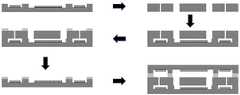
图1为本发明实施例提供的三明治式微机电系统真空封装的缓冲腔的结构示意图;FIG. 1 is a schematic structural diagram of a buffer cavity of a sandwich-type MEMS vacuum package according to an embodiment of the present invention;
图2为本发明实施例提供的三明治式微机电系统真空封装的缓冲腔的上层整体封装示意图;FIG. 2 is a schematic diagram of the overall package of the upper layer of the buffer cavity of the vacuum package of the sandwich MEMS according to an embodiment of the present invention;
图3为本发明实施例提供的三明治式微机电系统真空封装的缓冲腔的中层整体封装示意图;FIG. 3 is a schematic diagram of the overall package of the middle layer of the buffer cavity of the vacuum package of the sandwich MEMS according to the embodiment of the present invention;
图4为本发明实施例提供的三明治式微机电系统真空封装的缓冲腔的下层整体封装示意图;FIG. 4 is a schematic diagram of the overall package of the lower layer of the buffer cavity of the vacuum package of the sandwich MEMS according to the embodiment of the present invention;
图5为本发明实施例提供的三明治式微机电系统真空封装的缓冲腔的下盖和中间层键合,其整体再与上盖键合的封装过程示意图。5 is a schematic diagram of an encapsulation process in which the lower cover and the middle layer of the buffer chamber of the vacuum packaging of the sandwich-type MEMS system according to the embodiment of the present invention are bonded, and the whole is then bonded to the upper cover.
其中,1为上层,2为中层,3为下层,4为第一层封装环,5为第二层封装环,6为主腔体,7为缓冲腔,8为中层贯通孔,9为吸气剂。Among them, 1 is the upper layer, 2 is the middle layer, 3 is the lower layer, 4 is the first layer packaging ring, 5 is the second layer packaging ring, 6 is the main cavity, 7 is the buffer cavity, 8 is the middle layer through hole, 9 is the suction aerosol.
具体实施方式Detailed ways
为了使本发明的目的、技术方案及优点更加清楚明白,以下结合附图及实施例,对本发明进行进一步详细说明。应当理解,此处所描述的具体实施例仅仅用以解释本发明,并不用于限定本发明。In order to make the objectives, technical solutions and advantages of the present invention clearer, the present invention will be further described in detail below with reference to the accompanying drawings and embodiments. It should be understood that the specific embodiments described herein are only used to explain the present invention, but not to limit the present invention.
本发明提供了一种用于在完成三明治式MEMS器件真空封装过程中为保证封装寿命而设计的缓冲腔及其封装方法,通过对封装环进行单独处理,可以解决微电子器件内部腔体气压上升速度过快的问题。The invention provides a buffer cavity and a packaging method for ensuring the life of the package in the process of completing the vacuum packaging of the sandwich MEMS device. Too fast problem.
对于需要真空封装的微电子器件而言,其寿命与其腔体的压强直接相关,过高的压强会影响器件性能甚至无法正常工作。因此,对于真空封装,其寿命指标是十分重要的。为了提升器件的寿命,即降低气体向主腔体内泄漏的速度,需要良好的键合水平,优秀的吸气剂充当气体泵浦,存储泄漏气体。在本发明中,提出了一种器件结构上的设计,通过创建一个缓冲腔,使得气体首先向缓冲腔内泄漏,被吸气剂吸附,之后才会向主腔体内泄漏,从而延长了器件的寿命。为了保证缓冲腔体的体积,平衡吸气剂的压力以及吸气剂的沉积量,采用贯通孔连接三层键合器件的上下层缓冲腔,形成一个整体的腔体。For microelectronic devices that require vacuum packaging, their lifespan is directly related to the pressure of their cavity. Excessive pressure will affect the performance of the device or even fail to work properly. Therefore, for vacuum packaging, its life index is very important. To increase the lifetime of the device, i.e. reduce the rate of gas leakage into the main cavity, a good level of bonding is required, and a good getter acts as a gas pump to store the leaked gas. In the present invention, a structural design of the device is proposed. By creating a buffer cavity, the gas first leaks into the buffer cavity and is adsorbed by the getter, and then leaks into the main cavity, thereby prolonging the life of the device. life. In order to ensure the volume of the buffer cavity, balance the pressure of the getter and the deposition amount of the getter, through holes are used to connect the upper and lower buffer cavities of the three-layer bonding device to form a whole cavity.
图1示出了本发明实施例提供的三明治式微机电系统的圆晶级真空封装腔,为了便于说明,仅示出了与本发明实施例相关的部分,详述如下:FIG. 1 shows a wafer-level vacuum packaging cavity of a sandwich-type MEMS system provided by an embodiment of the present invention. For the convenience of description, only the part related to the embodiment of the present invention is shown, and the details are as follows:
本发明实施例提供的圆晶级真空封装腔包括:最内部的主腔体,用以提供工作器件的真空工作环境。其盖板位置沉积大量吸气剂,用以主腔体的气体压强维持。环绕主腔体为第一层封装环,其封装环在上下盖板位置处一一对应,以保证上下盖板上刻蚀的凹槽,即缓冲腔上下对应,以便于贯穿通孔链接。其贯穿通孔位置应在缓冲腔的中间位置,以保证避开其他应力集中的位置。通过在缓冲腔底部沉积吸气剂,用以延缓缓冲腔的压强上升的速度。缓冲腔外环绕为第二层封装环,与第一层封装环相似,我们也需要保证第二层封装环的位置对于上下盖板而言一一对应,以保证键合的对顶强度,以及器件的规则性,从而方便圆片级键合之后的切片。The wafer-level vacuum packaging cavity provided by the embodiment of the present invention includes: an innermost main cavity, which is used to provide a vacuum working environment for the working device. A large amount of getter is deposited at the position of the cover plate to maintain the gas pressure of the main cavity. Surrounding the main cavity is the first layer of packaging rings, the packaging rings are in one-to-one correspondence at the positions of the upper and lower cover plates to ensure that the grooves etched on the upper and lower cover plates, that is, the buffer chambers correspond up and down, so as to facilitate the connection of through holes. The position of the through hole should be in the middle of the buffer cavity to avoid other stress concentration positions. By depositing a getter at the bottom of the buffer chamber, the pressure rise speed of the buffer chamber is slowed down. The buffer cavity is surrounded by a second layer of packaging rings. Similar to the first layer of packaging rings, we also need to ensure that the positions of the second layer of packaging rings are in one-to-one correspondence with the upper and lower cover plates to ensure the bonding strength to the top, and regularity of the device, thereby facilitating slicing after wafer-level bonding.
如图2所示,对于器件的上层,形状一般为方形,其主腔体的上层与缓冲腔的上层沉积吸气剂,此处采用Ti基吸气剂,Ti表面沉积20nm的Au以充当牺牲层,防止Ti吸气剂氧化,并在键合加温时完成吸气剂的激活,用以保证缓冲腔的腔体压强上升不会太快。其中缓冲腔和主腔体之间的封装环,保持窄于中间层封装环的宽度,其差值与器件制作时的光刻精度相关,以保证键合时,上层的封装环能完整附着在中间层的封装环上。As shown in Figure 2, for the upper layer of the device, the shape is generally square, and the upper layer of the main cavity and the upper layer of the buffer cavity are deposited with getters. Here, a Ti-based getter is used, and 20 nm of Au is deposited on the surface of Ti to act as a sacrificial layer to prevent the oxidation of the Ti getter, and complete the activation of the getter when the bonding is heated, so as to ensure that the cavity pressure of the buffer cavity does not rise too fast. Among them, the packaging ring between the buffer cavity and the main cavity is kept narrower than the width of the middle layer packaging ring, and the difference is related to the lithography accuracy during device fabrication, so as to ensure that the upper packaging ring can be completely attached to the device during bonding. on the encapsulation ring of the middle layer.
如图3所示,对于器件的中间层,一般包括器件的主要运动模块,或者是其他需要真空环境才能正常工作的模块,保证器件功能的正常实现。与器件的上层封装环匹配,需要保证中间层的封装环的宽度,宽于上层的缓冲腔和主腔体之间的封装环,一般可保持差值在2μm以上,其差值与器件制作时的光刻精度相关,以保证键合时,上层的封装环能完整附着在中间层的封装环上。另外,中间层的缓冲腔的位置,需要蚀刻出贯穿通孔,其位置一般在器件缓冲腔的长边的居中位置,以保证避免器件的应力集中。As shown in Figure 3, the middle layer of the device generally includes the main motion module of the device, or other modules that require a vacuum environment to work normally, to ensure the normal realization of the device function. Matching with the upper packaging ring of the device, it is necessary to ensure that the width of the packaging ring in the middle layer is wider than the packaging ring between the upper buffer cavity and the main cavity. Generally, the difference can be maintained at more than 2μm, and the difference is the same as that of the device when the device is fabricated. The lithography accuracy is related to ensure that the packaging ring of the upper layer can be completely attached to the packaging ring of the middle layer during bonding. In addition, the position of the buffer cavity of the intermediate layer needs to be etched through through holes, which are generally located in the center of the long side of the buffer cavity of the device to avoid stress concentration of the device.
如图4所示,对于器件的下层,作为最初的封装模块,其封装环的宽度是最宽的,以满足键合顺序:下层-中层,键合好的器件再与上层键合。下层的封装环需要保证与中间层键合时的压力,二次键合的时候,需要保证与上层封装环键合时的压力。同样,与器件的上层一样,需要在主腔体和缓冲腔的下部沉积吸气剂。同样沉积Ti-Au吸气剂,用以保证缓冲腔的腔体压强上升不会太快。As shown in Figure 4, for the lower layer of the device, as the initial packaging module, the width of the packaging ring is the widest to meet the bonding sequence: lower layer-middle layer, and the bonded device is then bonded to the upper layer. The lower encapsulation ring needs to ensure the pressure when bonding with the middle layer, and during the secondary bonding, it needs to ensure the pressure when bonding with the upper encapsulation ring. Also, as with the upper layers of the device, the getter needs to be deposited in the lower part of the main cavity and the buffer cavity. A Ti-Au getter is also deposited to ensure that the cavity pressure of the buffer cavity does not rise too fast.
本发明提供的缓冲腔技术与现有技术相比,实现了圆晶级真空封装腔从双层圆片级封装到三明治式微机电系统的真空封装的突破。通过上下层同时沉积吸气剂,延缓了缓冲腔的真空度上升的速度。利用中间层的贯穿通孔,提升了缓冲腔的体积,平衡了由于上下键合面的漏率不同带来的缓冲腔上下层的吸气剂压力差异。另外对于吸气剂,本发明中的吸气剂能力更好,通过吸气剂的牺牲层,保证了吸气剂在工作前,不会出现工艺步骤中的损耗;且在键合时,能够同时完成吸气剂的激活,工艺步骤更简单。其封装工艺也更加简单,相比较于没有缓冲腔的设计,制作工艺并没有特别的变化,因此相对于现有技术,工艺兼容性有相当的优势。而封装步骤中的工艺兼容性,能保证更好的封装效果,保证更低的器件漏率。Compared with the prior art, the buffer cavity technology provided by the present invention achieves a breakthrough in the vacuum packaging of the wafer-level vacuum packaging cavity from double-layer wafer-level packaging to the vacuum packaging of the sandwich-type micro-electromechanical system. By simultaneously depositing the getter in the upper and lower layers, the rising speed of the vacuum degree of the buffer chamber is delayed. The use of the through-holes in the middle layer increases the volume of the buffer cavity and balances the difference in the getter pressure between the upper and lower layers of the buffer cavity due to the different leakage rates of the upper and lower bonding surfaces. In addition, for the getter, the getter capability of the present invention is better, and the sacrificial layer of the getter ensures that the getter will not be lost in the process steps before working; and during bonding, it can be At the same time, the activation of the getter is completed, and the process steps are simpler. The packaging process is also simpler. Compared with the design without a buffer cavity, the manufacturing process has no special change, so compared with the existing technology, the process compatibility has a considerable advantage. The process compatibility in the packaging step can ensure better packaging effect and lower device leakage rate.
本发明还提供了一种基于上述缓冲腔的真空封装方法,包括如下步骤:The present invention also provides a vacuum packaging method based on the above buffer chamber, comprising the following steps:
对于器件的上盖,通过干法刻蚀或者湿法刻蚀,完成缓冲腔的蚀刻,通过掩膜光刻和电子束热蒸发,完成封装环的沉积。通过电子束热蒸发或者磁控溅射,在缓冲腔的底部或者下盖的中央位置,完成吸气剂的沉积。For the top cover of the device, the buffer cavity is etched by dry etching or wet etching, and the encapsulation ring is deposited by mask lithography and electron beam thermal evaporation. The deposition of the getter is accomplished at the bottom of the buffer chamber or at the center of the lower cover by electron beam thermal evaporation or magnetron sputtering.
对于器件的中间层,通过干法或者湿法刻蚀,在多层缓冲腔的夹层硅片位置,完成贯穿刻蚀,贯通孔不需很大,仅仅起到连通上下盖板的作用。注意不要影响到器件的键合位置。For the middle layer of the device, dry or wet etching is used to complete the through-etching at the position of the interlayer silicon wafer in the multi-layer buffer cavity. Be careful not to affect the bonding position of the device.
对于器件的下盖,通过干法刻蚀或者湿法刻蚀,完成缓冲腔的蚀刻,通过掩膜光刻和电子束热蒸发,完成封装环的沉积。通过电子束热蒸发或磁控溅射,在缓冲腔的底部或者下盖的中央位置,完成吸气剂的沉积。For the lower cover of the device, the buffer cavity is etched by dry etching or wet etching, and the encapsulation ring is deposited by mask lithography and electron beam thermal evaporation. The deposition of the getter is accomplished at the bottom of the buffer chamber or at the center of the lower cover by electron beam thermal evaporation or magnetron sputtering.
对于上盖-中间层-下盖的键合顺序,决定了封装环的衬底宽度,为了保证器件的键合精度和键合强度,需要给出键合的余量。For the bonding sequence of the upper cover-intermediate layer-lower cover, the substrate width of the packaging ring is determined. In order to ensure the bonding accuracy and bonding strength of the device, the bonding margin needs to be given.
优选地,上盖板、中间层和下盖板可以采用高纯硅材料;硅作为半导体产业中被广泛应用的材料,在微尺寸下,硅的强度仍然能够保持,在器件尺寸很小的情况下,封装环的尺寸更小,而高纯硅能够保证器件的键合强度。Preferably, the upper cover plate, the middle layer and the lower cover plate can be made of high-purity silicon material; silicon is a widely used material in the semiconductor industry, and the strength of silicon can still be maintained at micro-scale. In the case of small device size The size of the package ring is smaller, and the high-purity silicon can ensure the bonding strength of the device.
优选地,本发明方法还包括利用在上下盖以及缓冲腔的内壁沉积吸气剂,延长缓冲腔的压强上升时间,外界气体始终在向器件内部泄漏或者是渗透,吸气剂具体作用在于,将泄漏进入器件内部的气体,包括水汽和空气,通过物理吸附或者化学吸附,将气体吸附在吸气剂表面,并通过扩散,将吸气剂表面的气体向吸气剂底部输运,维持吸气剂表面的吸附能力。通过这种方式,能较长时间的维持缓冲腔的压强水平。更低的缓冲腔压强水平,能够使得缓冲腔内的气体向主腔体泄漏的速度更慢,从而减缓主腔体压强上升的速度,从而维持器件的寿命。Preferably, the method of the present invention further includes depositing a getter on the upper and lower covers and the inner wall of the buffer cavity to prolong the pressure rise time of the buffer cavity, and the external gas always leaks or penetrates into the device. The gas leaked into the device, including water vapor and air, is adsorbed on the surface of the getter by physical adsorption or chemical adsorption, and the gas on the surface of the getter is transported to the bottom of the getter by diffusion to maintain the getter adsorption capacity on the surface of the agent. In this way, the pressure level of the buffer chamber can be maintained for a longer period of time. A lower pressure level of the buffer chamber can make the gas in the buffer chamber leak more slowly to the main chamber, thereby slowing down the speed of pressure rise in the main chamber, thereby maintaining the life of the device.
优选地,当下盖先于中间层键合,然后再与上盖键合,则下盖的封装环需要留出余量,其值与键合设备的对准精度相关。例如光刻和键合对准精度为2um,则上下封装环的设计时,可以将其下层拓宽2um,以保证键合过程中,中间层和下层能精准对齐,防止封装环悬空。Preferably, the lower cover is bonded before the middle layer, and then is bonded with the upper cover, the encapsulation ring of the lower cover needs to leave a margin, and the value is related to the alignment accuracy of the bonding equipment. For example, if the lithography and bonding alignment accuracy is 2um, when designing the upper and lower packaging rings, the lower layer can be widened by 2um to ensure that the middle layer and the lower layer can be accurately aligned during the bonding process and prevent the packaging ring from hanging.
当上盖先于中间层键合,然后再与下盖键合,则上盖的封装环需要留出余量,其值与键合设备的对准精度相关。When the upper cover is bonded before the middle layer, and then is bonded with the lower cover, the encapsulation ring of the upper cover needs to leave a margin, and its value is related to the alignment accuracy of the bonding equipment.
进一步优选地,对缓冲腔和主腔体的吸气剂选择Ti基吸气剂,吸气剂展现了对氧气和氢气和水汽有良好的吸附能力。Ti表面沉积20nm的Au以充当牺牲层,防止Ti吸气剂氧化,并在键合加温时完成吸气剂的激活,通过电子束热蒸发或者磁控溅射沉积,例如磁控溅射沉积过程的工艺参数为:气体流量Ar为20sccm,功率控制在250W,溅射时压强为1mtorr,温度控制在25℃。Further preferably, a Ti-based getter is selected for the getter in the buffer cavity and the main cavity, and the getter exhibits good adsorption capacity for oxygen, hydrogen and water vapor. 20nm of Au is deposited on the Ti surface to act as a sacrificial layer to prevent oxidation of the Ti getter, and to complete the activation of the getter when the bonding is heated, by electron beam thermal evaporation or magnetron sputter deposition, such as magnetron sputter deposition The process parameters of the process are: the gas flow rate Ar is 20 sccm, the power is controlled at 250 W, the pressure during sputtering is 1 mtorr, and the temperature is controlled at 25 °C.
优选地,晶圆键合可以通过硅硅直接键合或者金金热压键合或者铜铜热压键合,完成键合。对于硅硅直接键合,键合结果能够达到体硅强度,但是需要硅与硅的表面粗糙度十分光滑。由于在下层和中间层的键合之前经历的工艺步骤很少,对键合表面的影响更低,能够保证封装键合的质量,因此选择硅硅直接键合的方式,得到更低的漏率和更高的键合强度。而金金热压键合或者铜铜热压键合,对键合表面的粗糙度更加包容,而且键合效果也佳,能够满足更低的漏率,因此应用于中间层和上层的键合中,且在键合过程中,通过加热环境能够完成吸气剂的激活,简化工艺流程。Preferably, the wafer bonding can be accomplished by silicon-silicon direct bonding, gold-gold thermocompression bonding, or copper-copper thermocompression bonding. For silicon-silicon direct bonding, the bonding result can reach the strength of bulk silicon, but the surface roughness of silicon-to-silicon is required to be very smooth. Since there are few process steps before the bonding of the lower layer and the middle layer, the impact on the bonding surface is lower, and the quality of the package bonding can be guaranteed. Therefore, the silicon-silicon direct bonding method is selected to obtain a lower leakage rate. and higher bond strength. Gold-gold thermocompression bonding or copper-copper thermocompression bonding is more tolerant to the roughness of the bonding surface, and the bonding effect is also good, which can meet the lower leakage rate, so it is applied to the bonding of the middle layer and the upper layer. In the bonding process, the activation of the getter can be completed by heating the environment, which simplifies the process flow.
本发明提出的缓冲腔是针对零级封装的设计;采用缓冲腔将主腔体与外界的气压差减小,以台阶形式上升;并将上下两个腔体通过贯穿通孔打通,使得缓冲腔的体积得到提升,由于上下键合方式选择不同,两个键合面存在不相同的漏率。通过贯穿通孔,连接上下两个缓冲腔室,使其平衡上下缓冲腔中两个吸气剂面的压力,增强其减缓主腔体气压上升速度的效果,在三层键合的下层向下刻蚀凹坑,扩大主腔体的体积,并在底部沉积吸气剂,增大吸气剂的体积,延长器件寿命。The buffer cavity proposed by the invention is designed for zero-level packaging; the buffer cavity is used to reduce the air pressure difference between the main cavity and the outside world, and rises in the form of steps; the upper and lower cavities are opened through the through holes, so that the buffer cavity is Due to the different selection of upper and lower bonding methods, the two bonding surfaces have different leakage rates. Connect the upper and lower buffer chambers through the through holes to balance the pressure of the two getter surfaces in the upper and lower buffer chambers and enhance the effect of slowing down the air pressure rise in the main chamber. The pits are etched to expand the volume of the main cavity, and getter is deposited at the bottom to increase the volume of the getter and prolong the life of the device.
为了更进一步的说明本发明实施例,现参照附图并结合具体实例详述如下:In order to further illustrate the embodiments of the present invention, with reference to the accompanying drawings and specific examples are described in detail as follows:
(1)如图2所示,对于真空封装的器件的下层,首先在硅片内表面涂覆光刻胶充当掩膜,经历光刻以及显影,利用等离子体的深刻蚀,将主腔体以及缓冲腔的腔体刻蚀出来。一般而言,封装环的宽度可以设定在10um-15um,使得能够得到良好的键合效果,良好的漏率和更小的器件尺寸。之后利用磁控溅射或者电子束热蒸发,以磁控溅射为例,其工艺参数为:气体流量Ar为20sccm,功率控制在250W,溅射时压强为1mtorr,温度控制在25℃,完成Ti基吸气剂的沉积,之后再完成Au牺牲层的沉积,保护Ti,整个过程均在磁控溅射镀膜机中进行,其内部真空度保证了Ti吸气剂在被Au层保护之前不被氧化。如果采用电子束热蒸发,则原理相同。(1) As shown in Figure 2, for the lower layer of the vacuum-packaged device, first coat the inner surface of the silicon wafer with photoresist as a mask, undergo photolithography and development, and use the deep etching of plasma to remove the main cavity and The cavity of the buffer chamber is etched out. Generally speaking, the width of the package ring can be set at 10um-15um, so that good bonding effect, good leakage rate and smaller device size can be obtained. Then magnetron sputtering or electron beam thermal evaporation is used. Taking magnetron sputtering as an example, the process parameters are: the gas flow rate Ar is 20sccm, the power is controlled at 250W, the pressure during sputtering is 1mtorr, and the temperature is controlled at 25 ℃. The deposition of Ti-based getter, followed by the deposition of Au sacrificial layer to protect Ti, the whole process is carried out in a magnetron sputtering coater, and its internal vacuum ensures that the Ti getter will not be protected by the Au layer before it is protected. Oxidized. The principle is the same if electron beam thermal evaporation is used.
(2)如图3所示,首先在硅片内表面涂覆光刻胶充当掩膜,经历光刻以及显影,利用等离子体的深刻蚀,将主腔体和工作模块以及链接上下缓冲腔的贯穿通孔刻蚀出来。贯穿通孔位置一般在中间层的两层封装环的中间,目的是为了避免应力集中。针对不同的器件而言,贯穿通孔位置不同,但是核心思想为避免应力集中,保证器件的键合质量和本身强度。(2) As shown in Figure 3, first coat the inner surface of the silicon wafer with photoresist as a mask, undergo photolithography and development, and use the deep etching of plasma to connect the main cavity and the working module as well as the upper and lower buffer cavities. Through holes are etched out. The position of the through-hole is generally in the middle of the two-layer packaging ring of the intermediate layer, in order to avoid stress concentration. For different devices, the positions of the through holes are different, but the core idea is to avoid stress concentration and ensure the bonding quality and strength of the device.
(3)如图4所示,对于真空封装的器件的上层,首先在硅片内表面涂覆光刻胶充当掩膜,经历光刻以及显影,利用等离子体的深刻蚀,将主腔体以及缓冲腔的腔体刻蚀出来;一般而言,封装环的宽度可以设定在10um-15um,使得能够得到良好的键合效果,良好的漏率和更小的器件尺寸。然后利用相同工艺,依靠掩膜以及光刻显影,完成键合层的Au层沉积。之后利用磁控溅射或者电子束热蒸发镀Ti吸气剂,以磁控溅射为例,其工艺参数为:气体流量Ar为20sccm,功率控制在250W,溅射时压强为1mtorr,温度控制在25℃,完成Ti基吸气剂的沉积,之后再完成Au牺牲层的沉积,保护Ti,整个过程均在磁控溅射镀膜机中进行,其内部真空度保证了Ti吸气剂在被Au层保护之前不被氧化。如果采用电子束热蒸发,则原理相同。(3) As shown in Figure 4, for the upper layer of the vacuum-packaged device, first coat the inner surface of the silicon wafer with photoresist as a mask, undergo photolithography and development, and use the deep etching of plasma to remove the main cavity and The cavity of the buffer cavity is etched; generally, the width of the package ring can be set at 10um-15um, so that good bonding effect, good leak rate and smaller device size can be obtained. Then, using the same process, relying on mask and photolithography development, the deposition of the Au layer of the bonding layer is completed. Then, magnetron sputtering or electron beam thermal evaporation is used to coat Ti getter. Taking magnetron sputtering as an example, the process parameters are: the gas flow Ar is 20sccm, the power is controlled at 250W, the pressure during sputtering is 1mtorr, and the temperature is controlled At 25°C, the deposition of the Ti-based getter was completed, and then the deposition of the Au sacrificial layer was completed to protect the Ti. The whole process was carried out in a magnetron sputtering coater, and its internal vacuum ensured that the Ti getter was kept in place. The Au layer protects from being oxidized before. The principle is the same if electron beam thermal evaporation is used.
(4)如图5所示,将制作好的器件下层与中间层,利用硅硅直接键合方式,在键合机下进行对准,键合温度350℃,键合压力6000mbar,键合时间为一个小时,键合成为一个整体,之后在中间层的封装环位置,沉积Au,做好与器件上层进行金金直接键合的准备。同样,将其与器件上层在键合机中进行对准,键合温度450℃,键合压力7000mbar,键合时间一个小时。在键合过程中,由键合机内部分子泵抽真空,完成封装之后,键合机真空度即为器件初始真空度。而键合的加热过程,能够同时完成Ti基吸气剂表面的Au牺牲层的消耗扩散,从而露出被保护的Ti吸气剂,简化了工艺流程,保证了吸气剂的性能。(4) As shown in Figure 5, the lower layer and the middle layer of the fabricated device are aligned under the bonding machine using the silicon-silicon direct bonding method. The bonding temperature is 350 °C, the bonding pressure is 6000 mbar, and the bonding time After one hour, the bonding was integrated into a whole, and then Au was deposited on the package ring position of the middle layer to prepare for direct gold-gold bonding with the upper layer of the device. Similarly, align it with the upper layer of the device in a bonding machine, the bonding temperature is 450°C, the bonding pressure is 7000 mbar, and the bonding time is one hour. During the bonding process, the vacuum is pumped by the molecular pump inside the bonding machine. After the packaging is completed, the vacuum degree of the bonding machine is the initial vacuum degree of the device. The bonding heating process can simultaneously complete the consumption and diffusion of the Au sacrificial layer on the surface of the Ti-based getter, thereby exposing the protected Ti getter, simplifying the process flow, and ensuring the performance of the getter.
(5)由于键合顺序为下层和中层先键合,键合成型之后,再与上层键合。工艺中保证下层缓冲腔的封装环宽度大于上层缓冲腔封装环宽度,因此,在器件设计时,需要考虑给器件的下层余量,其大小与光刻和键合的对准精度相关。例如,若光刻和对准过程中,误差为2um,则设计时下层封装环的宽度应比上层大2um,以保证在产生误差时,中间层与下层的封装环,总是能够完整受力,不会因为误差产生悬空部分,从而确保良好的键合效果。同理,中间层与上层键合时,也应考虑这一点。(5) Since the bonding sequence is that the lower layer and the middle layer are bonded first, and then the upper layer is bonded after the bonding is formed. In the process, it is ensured that the package ring width of the lower buffer cavity is larger than that of the upper buffer cavity. Therefore, when designing the device, it is necessary to consider the lower layer margin for the device, and its size is related to the alignment accuracy of lithography and bonding. For example, if the error is 2um during the lithography and alignment process, the width of the lower layer packaging ring should be 2um larger than that of the upper layer during design to ensure that the middle layer and the lower layer packaging ring can always be fully stressed when errors occur. , there will be no dangling parts due to errors, so as to ensure a good bonding effect. Similarly, this should also be considered when bonding the middle layer to the upper layer.
本发明为三明治式真空封装的键合技术,与现有技术相比,对于吸气剂方面,利用牺牲层,提升了吸气剂的性能;对于器件设计方面,利用缓冲腔的设计,降低了吸气剂的压力,增大了对键合效果的容忍度,在下盖刻蚀出凹坑,增大了主腔体的体积,并在下盖位置沉积吸气剂,大幅增大了吸气剂的体积。同时通过中间层的贯穿通孔的设计,能够将器件的上下缓冲腔链接,平衡缓冲腔上下的吸气剂的压力。在追求更低的漏率显得很困难的时候,该技术能够明显提升器件的寿命。同时,这种技术的优势体现在,由于该技术仅仅通过增加了缓冲腔以及扩大了主腔体的体积,以及主腔体和缓冲腔中吸气剂的沉积,完成延缓主腔体气体的泄露因此,并没有与现行的MEMS工艺冲突,兼容性良好。对微机电系统表现为良好的普适性,很多器件的封装,都能通过这种方式获得寿命提升,应用意义大。The present invention is a bonding technology of sandwich type vacuum packaging. Compared with the prior art, for the getter, the sacrificial layer is used to improve the performance of the getter; for the device design, the design of the buffer cavity is used to reduce the performance of the getter. The pressure of the getter increases the tolerance of the bonding effect, and the lower cover is etched with pits, which increases the volume of the main cavity, and the getter is deposited at the lower cover, which greatly increases the size of the getter. volume of. At the same time, through the design of the through holes in the middle layer, the upper and lower buffer cavities of the device can be linked to balance the pressure of the getter on the upper and lower buffer cavities. At a time when the pursuit of lower leak rates is difficult, this technology can significantly improve device life. At the same time, the advantage of this technology is that, because this technology only increases the buffer cavity, expands the volume of the main cavity, and deposits the getter in the main cavity and the buffer cavity, it can delay the gas leakage of the main cavity. Therefore, there is no conflict with the current MEMS process, and the compatibility is good. It has good universality for MEMS. Many devices can be packaged in this way to improve their lifespan, which is of great application significance.
本领域的技术人员容易理解,以上所述仅为本发明的较佳实施例而已,并不用以限制本发明,凡在本发明的精神和原则之内所作的任何修改、等同替换和改进等,均应包含在本发明的保护范围之内。Those skilled in the art can easily understand that the above are only preferred embodiments of the present invention, and are not intended to limit the present invention. Any modifications, equivalent replacements and improvements made within the spirit and principles of the present invention, etc., All should be included within the protection scope of the present invention.
Claims (10)
Translated fromChinesePriority Applications (1)
| Application Number | Priority Date | Filing Date | Title |
|---|---|---|---|
| CN202210800894.7ACN115231509B (en) | 2022-07-08 | 2022-07-08 | Wafer-level vacuum packaging cavity of sandwich type micro-electromechanical system and packaging method |
Applications Claiming Priority (1)
| Application Number | Priority Date | Filing Date | Title |
|---|---|---|---|
| CN202210800894.7ACN115231509B (en) | 2022-07-08 | 2022-07-08 | Wafer-level vacuum packaging cavity of sandwich type micro-electromechanical system and packaging method |
Publications (2)
| Publication Number | Publication Date |
|---|---|
| CN115231509Atrue CN115231509A (en) | 2022-10-25 |
| CN115231509B CN115231509B (en) | 2024-07-16 |
Family
ID=83671210
Family Applications (1)
| Application Number | Title | Priority Date | Filing Date |
|---|---|---|---|
| CN202210800894.7AActiveCN115231509B (en) | 2022-07-08 | 2022-07-08 | Wafer-level vacuum packaging cavity of sandwich type micro-electromechanical system and packaging method |
Country Status (1)
| Country | Link |
|---|---|
| CN (1) | CN115231509B (en) |
Citations (6)
| Publication number | Priority date | Publication date | Assignee | Title |
|---|---|---|---|---|
| EP1834924A2 (en)* | 2006-03-16 | 2007-09-19 | Commissariat A L'energie Atomique | Packaging of a microelectronic component, in particular a MEMS, in an airtight cavity |
| CN101301993A (en)* | 2007-05-11 | 2008-11-12 | 北京大学 | A kind of MEMS device vacuum packaging method |
| US20090309203A1 (en)* | 2008-06-16 | 2009-12-17 | Honeywell International Inc. | Getter on die in an upper sense plate designed system |
| CN103879950A (en)* | 2012-12-19 | 2014-06-25 | 微机电科技香港有限公司 | MEMS device vacuum packaging structure |
| CN104003352A (en)* | 2014-06-13 | 2014-08-27 | 中国科学院上海微系统与信息技术研究所 | Mixed wafer level vacuum packaging method and structure based on getter film |
| CN107572474A (en)* | 2017-08-22 | 2018-01-12 | 华中科技大学 | It is a kind of encapsulate spacing can high-precision control MEMS package structure and method for packing |
- 2022
- 2022-07-08CNCN202210800894.7Apatent/CN115231509B/enactiveActive
Patent Citations (6)
| Publication number | Priority date | Publication date | Assignee | Title |
|---|---|---|---|---|
| EP1834924A2 (en)* | 2006-03-16 | 2007-09-19 | Commissariat A L'energie Atomique | Packaging of a microelectronic component, in particular a MEMS, in an airtight cavity |
| CN101301993A (en)* | 2007-05-11 | 2008-11-12 | 北京大学 | A kind of MEMS device vacuum packaging method |
| US20090309203A1 (en)* | 2008-06-16 | 2009-12-17 | Honeywell International Inc. | Getter on die in an upper sense plate designed system |
| CN103879950A (en)* | 2012-12-19 | 2014-06-25 | 微机电科技香港有限公司 | MEMS device vacuum packaging structure |
| CN104003352A (en)* | 2014-06-13 | 2014-08-27 | 中国科学院上海微系统与信息技术研究所 | Mixed wafer level vacuum packaging method and structure based on getter film |
| CN107572474A (en)* | 2017-08-22 | 2018-01-12 | 华中科技大学 | It is a kind of encapsulate spacing can high-precision control MEMS package structure and method for packing |
Non-Patent Citations (2)
| Title |
|---|
| 汪学方;林栋;甘志银;刘胜;张鸿海;: "MEMS器件真空封装工艺、装备及真空度检测的研究", 中国机械工程, no. 08, 25 April 2007 (2007-04-25)* |
| 王成刚;汪学方;甘志银;林栋;张鸿海;刘胜;: "一种用于MEMS器件真空密封技术的电阻熔焊方法", 焊接技术, no. 02, 28 April 2008 (2008-04-28)* |
Also Published As
| Publication number | Publication date |
|---|---|
| CN115231509B (en) | 2024-07-16 |
Similar Documents
| Publication | Publication Date | Title |
|---|---|---|
| CN101554987B (en) | Wafer-grade vacuum encapsulation process for micro-electro-mechanical system | |
| CN106959106B (en) | A kind of fused silica micro-hemisphere resonant gyroscope based on SOI package and its processing method | |
| CN101554988B (en) | Wafer-level vacuum packaging method for micro-electromechanical systems | |
| US7786561B2 (en) | Encapsulated microcomponent equipped with at least one getter | |
| CN102862947B (en) | A kind of MEMS and wafer-level vacuum encapsulating method thereof | |
| US10384932B2 (en) | Device including micromechanical components in cavities having different pressures and method for its manufacture | |
| JP4840771B2 (en) | Method for manufacturing mechanical quantity sensor | |
| CN102209683B (en) | MEMS device packaging with sidewall leakage protection | |
| CN101723308B (en) | MEMS wafer level vacuum packaging process | |
| US20130207281A1 (en) | Microelectronic substrate comprising a layer of buried organic material | |
| US20060228869A1 (en) | MEMS packaging structure and methods | |
| CN103162727B (en) | Sensing device and manufacturing method thereof | |
| CN115231509A (en) | Wafer level vacuum packaging cavity and packaging method of sandwich type micro-electromechanical system | |
| CN109786270A (en) | A kind of packaging and its manufacturing method | |
| US20160229687A1 (en) | Chip package and fabrication method thereof | |
| US10221063B2 (en) | Multi-level getter structure and encapsulation structure comprising such a multi-level getter structure | |
| CN114477074A (en) | Wafer-level atomic gas chamber processing method and device based on MEMS technology | |
| CN113636522A (en) | Airtight packaging structure of device with cavity and manufacturing method | |
| CN104058367A (en) | Manufacturing method of MEMS device | |
| US10910667B2 (en) | Microelectronic device | |
| CN108217579A (en) | Wafer level high vacuum leadless packaging method based on silica glass anode linkage | |
| CN114291785A (en) | Preparation method of sandwich accelerometer based on GIS cover plate | |
| CN103910325B (en) | High-reliability micro-electromechanical system (MEMS) packaging structure and method capable of achieving accurate control of bonding gap | |
| JP7404558B2 (en) | MEMS hermetic sealing device and method | |
| JP7696372B2 (en) | MEMS device manufacturing method and MEMS device |
Legal Events
| Date | Code | Title | Description |
|---|---|---|---|
| PB01 | Publication | ||
| PB01 | Publication | ||
| SE01 | Entry into force of request for substantive examination | ||
| SE01 | Entry into force of request for substantive examination | ||
| GR01 | Patent grant | ||
| GR01 | Patent grant |