CN115216405A - Multilayer cascade neural network micro-fluidic chip and preparation method thereof - Google Patents
Multilayer cascade neural network micro-fluidic chip and preparation method thereofDownload PDFInfo
- Publication number
- CN115216405A CN115216405ACN202210809837.5ACN202210809837ACN115216405ACN 115216405 ACN115216405 ACN 115216405ACN 202210809837 ACN202210809837 ACN 202210809837ACN 115216405 ACN115216405 ACN 115216405A
- Authority
- CN
- China
- Prior art keywords
- layer
- chip
- microfluidic chip
- neural network
- microelectrode
- Prior art date
- Legal status (The legal status is an assumption and is not a legal conclusion. Google has not performed a legal analysis and makes no representation as to the accuracy of the status listed.)
- Pending
Links
Images


Classifications
- C—CHEMISTRY; METALLURGY
- C12—BIOCHEMISTRY; BEER; SPIRITS; WINE; VINEGAR; MICROBIOLOGY; ENZYMOLOGY; MUTATION OR GENETIC ENGINEERING
- C12M—APPARATUS FOR ENZYMOLOGY OR MICROBIOLOGY; APPARATUS FOR CULTURING MICROORGANISMS FOR PRODUCING BIOMASS, FOR GROWING CELLS OR FOR OBTAINING FERMENTATION OR METABOLIC PRODUCTS, i.e. BIOREACTORS OR FERMENTERS
- C12M23/00—Constructional details, e.g. recesses, hinges
- C12M23/02—Form or structure of the vessel
- C12M23/16—Microfluidic devices; Capillary tubes
- B—PERFORMING OPERATIONS; TRANSPORTING
- B01—PHYSICAL OR CHEMICAL PROCESSES OR APPARATUS IN GENERAL
- B01L—CHEMICAL OR PHYSICAL LABORATORY APPARATUS FOR GENERAL USE
- B01L3/00—Containers or dishes for laboratory use, e.g. laboratory glassware; Droppers
- B01L3/50—Containers for the purpose of retaining a material to be analysed, e.g. test tubes
- B01L3/502—Containers for the purpose of retaining a material to be analysed, e.g. test tubes with fluid transport, e.g. in multi-compartment structures
- B01L3/5027—Containers for the purpose of retaining a material to be analysed, e.g. test tubes with fluid transport, e.g. in multi-compartment structures by integrated microfluidic structures, i.e. dimensions of channels and chambers are such that surface tension forces are important, e.g. lab-on-a-chip
- B01L3/502707—Containers for the purpose of retaining a material to be analysed, e.g. test tubes with fluid transport, e.g. in multi-compartment structures by integrated microfluidic structures, i.e. dimensions of channels and chambers are such that surface tension forces are important, e.g. lab-on-a-chip characterised by the manufacture of the container or its components
- C—CHEMISTRY; METALLURGY
- C12—BIOCHEMISTRY; BEER; SPIRITS; WINE; VINEGAR; MICROBIOLOGY; ENZYMOLOGY; MUTATION OR GENETIC ENGINEERING
- C12M—APPARATUS FOR ENZYMOLOGY OR MICROBIOLOGY; APPARATUS FOR CULTURING MICROORGANISMS FOR PRODUCING BIOMASS, FOR GROWING CELLS OR FOR OBTAINING FERMENTATION OR METABOLIC PRODUCTS, i.e. BIOREACTORS OR FERMENTERS
- C12M23/00—Constructional details, e.g. recesses, hinges
- C12M23/20—Material Coatings
- C—CHEMISTRY; METALLURGY
- C12—BIOCHEMISTRY; BEER; SPIRITS; WINE; VINEGAR; MICROBIOLOGY; ENZYMOLOGY; MUTATION OR GENETIC ENGINEERING
- C12M—APPARATUS FOR ENZYMOLOGY OR MICROBIOLOGY; APPARATUS FOR CULTURING MICROORGANISMS FOR PRODUCING BIOMASS, FOR GROWING CELLS OR FOR OBTAINING FERMENTATION OR METABOLIC PRODUCTS, i.e. BIOREACTORS OR FERMENTERS
- C12M23/00—Constructional details, e.g. recesses, hinges
- C12M23/34—Internal compartments or partitions
- C—CHEMISTRY; METALLURGY
- C12—BIOCHEMISTRY; BEER; SPIRITS; WINE; VINEGAR; MICROBIOLOGY; ENZYMOLOGY; MUTATION OR GENETIC ENGINEERING
- C12M—APPARATUS FOR ENZYMOLOGY OR MICROBIOLOGY; APPARATUS FOR CULTURING MICROORGANISMS FOR PRODUCING BIOMASS, FOR GROWING CELLS OR FOR OBTAINING FERMENTATION OR METABOLIC PRODUCTS, i.e. BIOREACTORS OR FERMENTERS
- C12M35/00—Means for application of stress for stimulating the growth of microorganisms or the generation of fermentation or metabolic products; Means for electroporation or cell fusion
- C12M35/02—Electrical or electromagnetic means, e.g. for electroporation or for cell fusion
- C—CHEMISTRY; METALLURGY
- C12—BIOCHEMISTRY; BEER; SPIRITS; WINE; VINEGAR; MICROBIOLOGY; ENZYMOLOGY; MUTATION OR GENETIC ENGINEERING
- C12M—APPARATUS FOR ENZYMOLOGY OR MICROBIOLOGY; APPARATUS FOR CULTURING MICROORGANISMS FOR PRODUCING BIOMASS, FOR GROWING CELLS OR FOR OBTAINING FERMENTATION OR METABOLIC PRODUCTS, i.e. BIOREACTORS OR FERMENTERS
- C12M41/00—Means for regulation, monitoring, measurement or control, e.g. flow regulation
- G—PHYSICS
- G01—MEASURING; TESTING
- G01N—INVESTIGATING OR ANALYSING MATERIALS BY DETERMINING THEIR CHEMICAL OR PHYSICAL PROPERTIES
- G01N27/00—Investigating or analysing materials by the use of electric, electrochemical, or magnetic means
- G—PHYSICS
- G01—MEASURING; TESTING
- G01N—INVESTIGATING OR ANALYSING MATERIALS BY DETERMINING THEIR CHEMICAL OR PHYSICAL PROPERTIES
- G01N33/00—Investigating or analysing materials by specific methods not covered by groups G01N1/00 - G01N31/00
- G01N33/48—Biological material, e.g. blood, urine; Haemocytometers
- G01N33/50—Chemical analysis of biological material, e.g. blood, urine; Testing involving biospecific ligand binding methods; Immunological testing
- G01N33/5005—Chemical analysis of biological material, e.g. blood, urine; Testing involving biospecific ligand binding methods; Immunological testing involving human or animal cells
- G01N33/5008—Chemical analysis of biological material, e.g. blood, urine; Testing involving biospecific ligand binding methods; Immunological testing involving human or animal cells for testing or evaluating the effect of chemical or biological compounds, e.g. drugs, cosmetics
- G01N33/5044—Chemical analysis of biological material, e.g. blood, urine; Testing involving biospecific ligand binding methods; Immunological testing involving human or animal cells for testing or evaluating the effect of chemical or biological compounds, e.g. drugs, cosmetics involving specific cell types
- G01N33/5058—Neurological cells
Landscapes
- Health & Medical Sciences (AREA)
- Chemical & Material Sciences (AREA)
- Life Sciences & Earth Sciences (AREA)
- Engineering & Computer Science (AREA)
- Bioinformatics & Cheminformatics (AREA)
- Zoology (AREA)
- Wood Science & Technology (AREA)
- Organic Chemistry (AREA)
- Biomedical Technology (AREA)
- General Health & Medical Sciences (AREA)
- Biotechnology (AREA)
- Biochemistry (AREA)
- Microbiology (AREA)
- Genetics & Genomics (AREA)
- Immunology (AREA)
- Sustainable Development (AREA)
- General Engineering & Computer Science (AREA)
- Analytical Chemistry (AREA)
- Clinical Laboratory Science (AREA)
- Physics & Mathematics (AREA)
- Hematology (AREA)
- Cell Biology (AREA)
- General Physics & Mathematics (AREA)
- Molecular Biology (AREA)
- Dispersion Chemistry (AREA)
- Urology & Nephrology (AREA)
- Chemical Kinetics & Catalysis (AREA)
- Pathology (AREA)
- Neurology (AREA)
- Neurosurgery (AREA)
- Toxicology (AREA)
- Tropical Medicine & Parasitology (AREA)
- Electromagnetism (AREA)
- Electrochemistry (AREA)
- Food Science & Technology (AREA)
- Medicinal Chemistry (AREA)
- Apparatus Associated With Microorganisms And Enzymes (AREA)
Abstract
Description
Translated fromChinese技术领域technical field
本发明涉及生物传感器的微加工领域以及生物细胞培养与检测领域,是一种多层级联的神经网络微流控芯片及其制备方法。The invention relates to the field of microfabrication of biosensors and the field of biological cell culture and detection, and relates to a multi-layer cascaded neural network microfluidic chip and a preparation method thereof.
背景技术Background technique
大脑是地球上最为复杂的结构体,大脑除了可感知外部世界,控制机体的反射活动外,还具有语言、学习、记忆和思维等高级功能。然而,人类对大脑功能的认知还十分有限。因此,深入了解大脑的复杂结构,对人类了解大脑并进而开发大脑具有十分重要的意义。The brain is the most complex structure on earth. In addition to perceiving the external world and controlling the body's reflex activities, the brain also has advanced functions such as language, learning, memory, and thinking. However, human understanding of brain function is still very limited. Therefore, a deep understanding of the complex structure of the brain is of great significance for human beings to understand the brain and then develop the brain.
神经电生理学研究是评价大脑功能的重要途径之一。而微加工技术制备的微电极阵列为神经电生理信息的记录和调控提供了一种高信噪比、高通量的手段,是研究神经科学、神经网络发育、神经信息编码、传导、响应和存储的机制研究、神经性疾病的治疗研究以及高通量药物筛选和神经药理学研究等众多领域中的重要研究工具。因此,将微电极阵列用于体外神经元网络电生理信息的检测已经成为理解大脑一些简单功能和潜在神经机制的重要手段。Neuroelectrophysiological research is one of the important ways to evaluate brain function. The microelectrode array prepared by micromachining technology provides a high signal-to-noise ratio and high-throughput means for the recording and regulation of neural electrophysiological information. It is an important research tool in many fields such as mechanistic studies of storage, therapeutic studies of neurological diseases, and high-throughput drug screening and neuropharmacological studies. Therefore, the use of microelectrode arrays for the detection of electrophysiological information in neuronal networks in vitro has become an important means to understand some simple functions and underlying neural mechanisms of the brain.
然而,现在对大脑功能的基本原理的理解仍是神经生理学研究中的一大重要挑战,由于高度的连通性,因此在大脑水平上进行这项研究会带来很高的复杂性。相反,单个或几个神经元的水平不能提供足够的功能连接。从这个意义上讲,体外对神经元网络的研究成为了解大脑高级功能最基本原理的途径之一。However, the current understanding of the fundamentals of brain function remains an important challenge in neurophysiological research, and conducting this research at the brain level entails a high level of complexity due to the high level of connectivity. Conversely, the level of a single or a few neurons does not provide sufficient functional connectivity. In this sense, the study of neuronal networks in vitro has become one of the ways to understand the most basic principles of higher brain functions.
基于微加工技术制备的微流控芯片可以精细化的制作出微小的流体结构,使得体外定制设计神经网络的连接成为可能。这为体外构建大脑的连接关系提供了方法。近年来,将微流控芯片与微电极阵列组合的神经芯片,因其具备检测与调控定制网络的神经电生理信息的能力,在研究脑神经机理上取得了重要成果。Microfluidic chips prepared based on micromachining technology can finely produce tiny fluid structures, making it possible to customize the connection of neural networks in vitro. This provides a way to build brain connections in vitro. In recent years, neural chips that combine microfluidic chips and microelectrode arrays have achieved important results in the study of brain neural mechanisms because of their ability to detect and regulate the neural electrophysiological information of customized networks.
发明内容SUMMARY OF THE INVENTION
本发明的目的是提供一种多层级联的神经网络微流控芯片及其制备方法。该芯片通过微流控的方法在微电极阵列上培养五个相对独立神经元网络,不同神经元网络之间通过微沟道产生突触连接,从而实现不同神经元网络之间的信息传递,并且通过突触控制室可以对微沟道中两个不同神经元网络之间形成的突触进行化学和物理上的调控。微流控芯片下的微电极阵列可以实现对这些神经元网络电生理动力学的评价,从而了解神经元网络之间的神经信息的传递及功能的实现。这些发明使得该芯片能够在实现大脑不同脑区的体外简单模拟,对了解神经元网络信息传递,进而认识大脑的高级功能的基本原理有重要意义。The purpose of the present invention is to provide a multi-layer cascaded neural network microfluidic chip and a preparation method thereof. The chip cultivates five relatively independent neuron networks on a microelectrode array by a microfluidic method, and synaptic connections are generated between different neuron networks through microchannels, thereby realizing information transmission between different neuron networks, and The synapse formed between two different neuronal networks in the microchannel can be chemically and physically regulated through the synaptic control chamber. The microelectrode array under the microfluidic chip can realize the evaluation of the electrophysiological dynamics of these neuronal networks, so as to understand the transmission of neural information and the realization of functions between neuronal networks. These inventions enable the chip to achieve simple in vitro simulation of different brain regions, which is of great significance for understanding the information transmission of neuronal networks, and then understanding the basic principles of advanced functions of the brain.
为实现这一目的,本发明采用如下技术方案:For realizing this purpose, the present invention adopts following technical scheme:
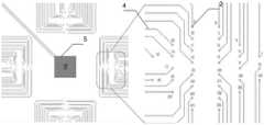
一种多层级联的神经网络微流控芯片,包括两层子芯片:第一层子芯片和第二层子芯片,其中第一层子芯片为第一层微电极阵列芯片,第二层子芯片为第二层微流控芯片;第一层微电极阵列芯片包括:绝缘基底、多个微电极、对电极、连接导线、接触位点及绝缘层;所述绝缘基底(1)是整个神经网络微流控芯片的载体;微电极(2)分四组,微电极位于微沟道(8)的两侧;每组微电极(2)周围都设有对电极(3);对电极(3)和微电极(2)均通过连接导线(4)延伸并连接到绝缘基底外围的接触位点(5);所有连接导线(4)表面均覆盖有绝缘层(6);A multi-layer cascaded neural network microfluidic chip includes two layers of sub-chips: a first layer of sub-chips and a second layer of sub-chips, wherein the first layer of sub-chips is a first-layer micro-electrode array chip, and the second layer of sub-chips The chip is a second-layer microfluidic chip; the first-layer microelectrode array chip includes: an insulating substrate, a plurality of microelectrodes, counter electrodes, connecting wires, contact sites and an insulating layer; the insulating substrate (1) is the entire neural The carrier of the network microfluidic chip; the microelectrodes (2) are divided into four groups, and the microelectrodes are located on both sides of the microchannel (8); each group of microelectrodes (2) is provided with a counter electrode (3) around it; 3) and the microelectrodes (2) are both extended through the connecting wires (4) and connected to the contact points (5) on the periphery of the insulating base; the surfaces of all the connecting wires (4) are covered with an insulating layer (6);
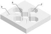
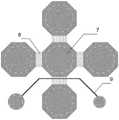
第二层微流控芯片包括:五个细胞培养槽、四组用于连接不同细胞培养槽的微沟道以及一组用于调控突触的突触控制室;突触控制室(9)能够用于对微沟道(8)中的生长的突触进行化学或物理学上的调控造模;在键合工艺下完成所述芯片的微电极阵列芯片与微流控芯片的封装。The second layer of microfluidic chip includes: five cell culture tanks, four groups of microchannels for connecting different cell culture tanks, and a group of synaptic control chambers for regulating synapses; the synaptic control chambers (9) can The method is used for chemically or physically regulating and modeling the synapses grown in the microchannel (8); the microelectrode array chip and the microfluidic chip of the chip are packaged under the bonding process.
所述两层子芯片为第一层微电极阵列芯片和第二层微流控芯片。The two-layer sub-chips are a first-layer microelectrode array chip and a second-layer microfluidic chip.
所述绝缘基底是整个神经网络微流控芯片的载体;微电极分四组,微电极位于微沟道的两侧;每组微电极周围都设有对电极;对电极和微电极均通过连接导线延伸并连接到绝缘基底外围的接触位点;所有连接导线表面均覆盖有绝缘层。The insulating substrate is the carrier of the entire neural network microfluidic chip; the microelectrodes are divided into four groups, and the microelectrodes are located on both sides of the microchannel; each group of microelectrodes is provided with a counter electrode; the counter electrode and the microelectrode are connected by The wires extend and connect to contact sites on the periphery of the insulating substrate; all connecting wires are covered with an insulating layer.
所述微流控芯片中的五个细胞培养槽用于培养神经细胞,并通过微沟道进行连接。而突触控制室可用于对微沟道中的生长的突触进行化学或物理学上的调控造模。The five cell culture tanks in the microfluidic chip are used for culturing nerve cells and are connected through microchannels. Synaptic control chambers can be used to chemically or physically modulate growing synapses in microchannels.
所述的一种多层级联的神经网络微流控芯片,所述微电极阵列芯片,绝缘基底的材料选用石英玻璃;微电极的材料是具备生物相容性的导电薄膜,可以为金、铂、氮化钛、铟锡氧化物和纳米线其中之一;绝缘层所使用材料为具备生物相容性的绝缘材料,为二氧化硅、氮化硅和SU8之一。In the multi-layer cascaded neural network microfluidic chip, the material of the microelectrode array chip is quartz glass; the material of the microelectrode is a biocompatible conductive film, which can be gold or platinum. , one of titanium nitride, indium tin oxide and nanowires; the material used in the insulating layer is a biocompatible insulating material, which is one of silicon dioxide, silicon nitride and SU8.
所述的一种多层级联的神经网络微流控芯片,所述微电极直径为5μm-30μm,微电极间距为50-500μm。In the multi-layer cascaded neural network microfluidic chip, the diameter of the micro-electrodes is 5 μm-30 μm, and the distance between the micro-electrodes is 50-500 μm.
所述的一种多层级联的神经网络微流控芯片,所述微流体芯片的五个细胞培养槽(7)相互独立,仅通过宽度约5-15μm,高度约5-15μm的微沟道(8)相连接,因此可以将培养在不同细胞培养槽(7)的神经元网络可以看作仅通过轴突与树突相连接的独立神经元网络,可将其简单模拟成大脑中的独立网络。In the multi-layer cascaded neural network microfluidic chip, the five cell culture tanks (7) of the microfluidic chip are independent of each other, and only pass through the microchannels with a width of about 5-15 μm and a height of about 5-15 μm (8) are connected, so the neuron network cultured in different cell culture tanks (7) can be regarded as an independent neuron network connected only by axons and dendrites, which can be simply simulated as an independent neuron network in the brain network.
所述的一种多层级联的神经网络微流控芯片,所述的第二层微流控芯片的材质是具有生物相容性的聚甲基硅氧烷或聚甲基丙烯酸甲酯。In the multi-layer cascaded neural network microfluidic chip, the material of the second layer of the microfluidic chip is biocompatible polymethylsiloxane or polymethylmethacrylate.
所述的一种多层级联的神经网络微流控芯片,所述的第二层微流控芯片的细胞培养槽(7)为圆孔,直径为4-8mm;微沟道(8)分四组,每组10-30条沟道,长度400-900μm,用于连接细胞培养槽。In the multi-layer cascaded neural network microfluidic chip, the cell culture tank (7) of the second layer of the microfluidic chip is a circular hole with a diameter of 4-8 mm; the microchannel (8) is divided into Four groups of 10-30 channels each with a length of 400-900 μm are used to connect cell culture tanks.
所述的一种多层级联的神经网络微流控芯片,所述的第二层微流控芯片的突触控制室(9)有大小不同的两个圆形调控室,直径为1-4mm,两者通过一条宽为20-50μm的沟道相连接。In the multi-layer cascaded neural network microfluidic chip, the synaptic control chamber (9) of the second layer of the microfluidic chip has two circular control chambers of different sizes, with a diameter of 1-4 mm , the two are connected by a channel with a width of 20-50μm.
所述的一种多层级联的神经网络微流控芯片,第一层微电极阵列芯片与第二层微流控芯片通过加热键合或者等离子键合的方式在对准仪器上将两个芯片进行贴合。In the multi-layer cascaded neural network microfluidic chip, the first layer of microelectrode array chip and the second layer of microfluidic chip are heated or plasma bonded to align the two chips on the aligning instrument. to fit.
本发明还提供一种制备如上任一项所述的神经网络微流控芯片的方法,包括制备第一层微电极阵列芯片和制备第二层微流控芯片;The present invention also provides a method for preparing the neural network microfluidic chip according to any one of the above, including preparing a first layer of microelectrode array chip and preparing a second layer of microfluidic chip;
制备第一层微电极阵列芯片,包括如下步骤:The preparation of the first-layer microelectrode array chip includes the following steps:
(1)清洗玻璃基底,获得表面清洁的绝缘基底(1);(1) cleaning the glass substrate to obtain an insulating substrate (1) with a clean surface;
(2)在经过清洗过的绝缘基底(1)上旋涂一层光刻胶,厚度为1-2μm,光刻显影后形成微电极(2)、对电极(3)、连接导线(4)和接触位点(5)的图案;(2) Spin-coat a layer of photoresist on the cleaned insulating substrate (1) with a thickness of 1-2 μm, and form microelectrodes (2), counter electrodes (3) and connecting wires (4) after photolithography and development and the pattern of contact sites (5);
(3)在光刻胶图案化的表面通过溅射沉积一层铂导层;可选地可预先溅射钛种子层,用于增加导电层基底的粘附性;(3) depositing a platinum conductive layer on the patterned surface of the photoresist by sputtering; optionally, a titanium seed layer can be sputtered in advance to increase the adhesion of the conductive layer substrate;
(4)采用剥离工艺在有机溶剂中去除多余的导电层,留下所需的微电极(2)、对电极(3)、连接导线(4)和接触位点(5);(4) removing the excess conductive layer in an organic solvent by a stripping process, leaving the required microelectrodes (2), counter electrodes (3), connecting wires (4) and contact sites (5);
(5)通过等离子体增强的化学气相沉积的方法在基底上沉积氧化硅或氮化硅绝缘层(6);(5) depositing a silicon oxide or silicon nitride insulating layer (6) on the substrate by means of plasma-enhanced chemical vapor deposition;
(6)通过光刻和等离子束刻蚀的方法,暴露出微电极(2)、对电极(3)和接触位点(5),保留所有连接导线(4)表面覆盖的绝缘层;(6) Expose the microelectrode (2), the counter electrode (3) and the contact site (5) by means of photolithography and plasma beam etching, and retain the insulating layer covered on the surface of all the connecting wires (4);
制备第二层微流控芯片,包括如下步骤:The preparation of the second-layer microfluidic chip includes the following steps:
(1)在经过清洗过的硅片上旋涂光刻胶,图形化出用于后续光刻的对准标记,接着通过溅射铂在硅片上生成对准标记;(1) spin-coating photoresist on the cleaned silicon wafer, pattern alignment marks for subsequent lithography, and then generate alignment marks on the silicon wafer by sputtering platinum;
(2)采用光刻胶通过光刻的工艺在硅片上光刻出微沟道(8);(2) photoresist is used to photoetch microchannels (8) on the silicon wafer by a photolithography process;
(3)在硅片上光刻出细胞培养槽(7)与突触控制室(9);(3) photoetching the cell culture tank (7) and the synapse control room (9) on the silicon wafer;
(4)光刻完毕后,在热板上加热完成坚模工艺,获得制作好的模具;(4) After the lithography is completed, heating on a hot plate to complete the die-setting process to obtain a manufactured die;
(5)将PDMS预聚物和催化剂混合倒入装模具的培养皿中,在真空干燥器中去除气泡后,加热固化;(5) Pour the PDMS prepolymer and the catalyst into the petri dish with the mold, remove the bubbles in the vacuum desiccator, and heat to solidify;
(6)将微流控器件从模具中分离,并用打孔器在微流控器件中制作出细胞培养槽(7)与突触控制室(9)。(6) The microfluidic device is separated from the mold, and a cell culture tank (7) and a synaptic control chamber (9) are fabricated in the microfluidic device with a punch.
进一步地,所述方法还包括如下步骤:将第一层微电极阵列芯片与第二层微流控芯片在氧离子清洁机中进行表面活化;活化后在对准仪器中间第一层微电极阵列芯片与第二层微流控芯片对齐获得最终的神经网络微流控芯片。Further, the method further includes the steps of: activating the first layer of microelectrode array chip and the second layer of microfluidic chip in an oxygen ion cleaning machine; after activation, aligning the first layer of microelectrode array in the middle of the instrument The chip is aligned with the second-layer microfluidic chip to obtain the final neural network microfluidic chip.
所述的一种多层级联的神经网络微流控芯片的试验方法,具体步骤如下:The described test method for a multi-layered neural network microfluidic chip, the specific steps are as follows:
(a)选择怀孕15-18天的ICR(Institute of Cancer Research)小鼠通过颈椎脱位安乐死,用75%酒精消毒孕鼠的腹部皮肤,然后用手术到去除子宫并放入预冷的HBSS缓冲液中。剥离胎鼠,剪下头部放入预冷的HBSS缓冲液。小心分离海马脑区,去除脑膜并切碎。(a) ICR (Institute of Cancer Research) mice at 15-18 days of pregnancy were selected to be euthanized by cervical dislocation, the abdominal skin of the pregnant mice was disinfected with 75% alcohol, and then the uterus was removed by surgery and placed in pre-chilled HBSS buffer middle. The fetal rat was stripped, and the head was cut off and placed in pre-chilled HBSS buffer. The hippocampal brain region was carefully isolated, the meninges removed and minced.
(b)剥离胎鼠的海马脑区置于DMEM缓冲液中解离15分钟。使用移液枪头轻轻吹打组织使其分散。收集缓冲液的上清液,在离心机中离心5分钟。用Neurobasal Plus Medium重悬细胞并使用血细胞计数器对重悬的细胞进行计数。(b) The hippocampal brain region of the stripped fetal rat was dissociated in DMEM buffer for 15 minutes. Disperse the tissue by gently pipetting with a pipette tip. The buffer supernatant was collected and centrifuged in a centrifuge for 5 minutes. Cells were resuspended in Neurobasal Plus Medium and counted using a hemocytometer.
(c)将神经细胞分别接种在所述芯片的不同细胞培养槽(7)上,神经细胞在体外培养2-3周,让相邻细胞培养槽(7)的轴树突在微沟道中形成突触连接以后进行电生理的检测。(c) Inoculating nerve cells on different cell culture tanks (7) of the chip, the nerve cells are cultured in vitro for 2-3 weeks, and the axonal dendrites in the adjacent cell culture tanks (7) are formed in the microchannels Electrophysiological measurements were performed after synaptic connections.
本发明提供的一种多层级联的神经网络微流控芯片及其制备方法,结合了微电极阵列和微流控的技术,能够在体外构建按照个人想法连接的神经元网络群,并且每个神经元网络内部相对独立,通过微电极阵列可以检测不同神经元网络之间的神经信息的流向。芯片还具备对突触区域精确控制与检测的功能,通过对突触控制区加入化学或物理刺激可以体外模拟突触损伤类连接的神经元网络。因此,本发明为大脑提供一个简化模型,对了解神经元网络信息传递,进而认识大脑的高级功能的基本原理有重要价值。The invention provides a multi-layer cascaded neural network microfluidic chip and a preparation method thereof, which combine the technology of microelectrode array and microfluidic control, and can construct a neuron network group connected according to personal ideas in vitro, and each The interior of the neuron network is relatively independent, and the flow of neural information between different neuron networks can be detected through the microelectrode array. The chip also has the function of precise control and detection of the synaptic area. By adding chemical or physical stimulation to the synaptic control area, the neuron network with synaptic damage-like connections can be simulated in vitro. Therefore, the present invention provides a simplified model for the brain, which is of great value for understanding the information transmission of the neuron network and further understanding the basic principles of the advanced functions of the brain.
附图说明Description of drawings
为了使本发明的目的、特点和优势更加清楚,下面结合图对本发明作进一步的详细描述,其中:In order to make the purpose, features and advantages of the present invention clearer, the present invention is described in further detail below in conjunction with the drawings, wherein:
图1为本发明一种多层级联的神经网络微流控芯片的结构示意图;1 is a schematic structural diagram of a multi-layered neural network microfluidic chip of the present invention;
图2为本发明一种多层级联的神经网络微流控芯片的第一层芯片微电极阵列芯片结构示意图;2 is a schematic structural diagram of a first-layer chip microelectrode array chip of a multi-layered neural network microfluidic chip of the present invention;
图3为本发明一种多层级联的神经网络微流控芯片的第一层芯片微电极阵列芯片局部放大图;FIG. 3 is a partial enlarged view of the first-layer chip microelectrode array chip of a multi-layer cascaded neural network microfluidic chip according to the present invention;
图4为本发明一种多层级联的神经网络微流控芯片的第二层芯片微流控芯片结构示意图;4 is a schematic structural diagram of a second-layer chip microfluidic chip of a multi-layer cascaded neural network microfluidic chip of the present invention;
图5为本发明一种集成微流控、微电极阵列的类脑功能第二层芯片微流控芯片平面示意图;5 is a schematic plan view of a second-layer chip microfluidic chip with a brain-like function integrated with microfluidics and a microelectrode array according to the present invention;
图6为本发明一种多层级联的神经网络微流控芯片的局部发大图;6 is a partial enlarged view of a multi-layered neural network microfluidic chip of the present invention;
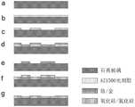
图7为本发明多层级联的神经网络微流控芯片的第一层微电极阵列芯片的制备方法工艺流程图;7 is a process flow diagram of a method for preparing a first-layer microelectrode array chip of a multi-layer cascaded neural network microfluidic chip of the present invention;
图7a为清洗石英玻璃片;Fig. 7a is cleaning quartz glass sheet;
图7b为石英玻璃片表面涂覆AZ1500型光刻胶;Figure 7b shows that the surface of the quartz glass sheet is coated with AZ1500 photoresist;
图7c为光刻AZ1500型光刻胶暴露出导电层图形;Figure 7c shows the pattern of the conductive layer exposed by photolithography of AZ1500 type photoresist;
图7d为溅射Ti/Pt导电层;Figure 7d shows the sputtered Ti/Pt conductive layer;
图7e为采用lift-off工艺形成导电层图形留下所需电极、引线及触点示意图;FIG. 7e is a schematic diagram of forming a conductive layer pattern by a lift-off process to leave required electrodes, leads and contacts;
图7f为PECVD沉积氧化硅和氮化硅;Figure 7f shows PECVD deposition of silicon oxide and silicon nitride;
图7g为刻蚀绝缘层获得微电极阵列芯片;Fig. 7g is a micro-electrode array chip obtained by etching the insulating layer;
附图标号说明:Description of reference numbers:
a为微电极阵列芯片,b为微流控芯片。a is a microelectrode array chip, and b is a microfluidic chip.
1为绝缘基底,2为微电极,3为对电极、4为连接导线、5为接触位点、6为绝缘层,7为细胞培养槽、8为微沟道,9为突触控制室。1 is an insulating substrate, 2 is a microelectrode, 3 is a counter electrode, 4 is a connecting wire, 5 is a contact site, 6 is an insulating layer, 7 is a cell culture tank, 8 is a microchannel, and 9 is a synaptic control chamber.
具体实施方式Detailed ways
以下结合附图和具体的实施例对本发明的技术方案做进一步描述。以下实施例不构成对本发明的限定。The technical solutions of the present invention will be further described below with reference to the accompanying drawings and specific embodiments. The following examples do not constitute a limitation of the present invention.
如图1、2和4为所示,本发明提供的一种多层级联的神经网络微流控芯片。整个芯片系统包括两层子芯片:第一层子芯片和第二层子芯片;其中第一层子芯片为第一层微电极阵列芯片,第二层子芯片为第二层微流控芯片。As shown in Figures 1, 2 and 4, the present invention provides a multi-layer cascaded neural network microfluidic chip. The whole chip system includes two layers of sub-chips: a first layer of sub-chips and a second layer of sub-chips; wherein the first layer of sub-chips is the first layer of micro-electrode array chips, and the second layer of sub-chips is the second layer of micro-fluidic chips.
第一层微电极阵列芯片a包括:绝缘基底1、多个微电极2、对电极3、连接导线4、接触位点5及绝缘层6。The first-layer microelectrode array chip a includes: an insulating
第二层微流控芯片b包括:五个细胞培养槽7、四组用于连接不同细胞培养槽的微沟道8以及一组用于调控突触的突触控制室9。The second layer of microfluidic chip b includes: five
绝缘基底1为玻璃基底。微电极2、对电极3、连接导线4、接触位点5、绝缘层6、细胞培养槽7、微沟道8以及突触控制室9设置在绝缘基底1上。微沟道8为微流控芯片沟道。突触控制室9为微流控芯片的突触控制室。The insulating
如图2、3所示,石英玻璃绝缘基底1是整个芯片系统的载体,厚度约为1.5mm,长度约为5cm,宽度约为5cm。微电极2分四组。微电极2在石英玻璃绝缘基底1的中央区域并分布于每组微沟道8的附近(图6),微电极2通过连接导线4连接到基底外围的接触位点5,微电极的直径约为20μm。微沟道8两侧的每组微电极2附近都设有对电极3。对电极3通过连接导线4延伸并连接到绝缘基底外围的接触位点5。所有连接导线4表面均覆盖有绝缘层6。As shown in FIGS. 2 and 3 , the quartz
如图4、5所示,所述第二层微流控芯片的细胞培养槽7为圆孔,细胞培养槽7是由于培养神经元网络的主体,其直径为4mm。五个细胞培养槽7用于培养神经细胞。微沟道8宽度约5-15μm,高度约5-15μm。As shown in FIGS. 4 and 5 , the
微沟道8用于连接不同的细胞培养槽7进而实现不同神经元网络之间产生定向连接。微沟道8分四组,每组10-30条沟道,长度400-900μm,用于连接细胞培养槽。所述微流体芯片的五个细胞培养槽7相互独立,仅通过微沟道8相连接,因此可以将培养在不同细胞培养槽7的神经元网络可以看作仅通过轴突与树突相连接的独立神经元网络,可将其简单模拟成大脑中的独立网络。The
例如,相邻的细胞培养槽7之间有20条微沟道,微沟道长、宽和高分别为600μm、10μm和5μm。突触控制室9由孔径为2μm和1.5μm一大一小两个圆孔与一条宽度为50μm的沟道组成,一大一小两个圆孔通过所述的一条宽度为50μm的沟道相连接。如图5所示,突触控制室9的沟道位于中央的细胞培养槽7和与中央细胞培养槽相连接的一个外围的细胞培养槽的微沟道8之间,突触控制室9的沟道距离中央和其中一个外围的细胞培养槽分别为200μm和400μm。突触控制室9能够用于对微沟道8中的生长的突触进行化学或物理学上的调控造模。如图6所示,微电极阵列芯片a与微流控芯片b在对准键合后,微电极阵列芯片a上的微电极2分四组,每组31个分布在微流控芯片b的微沟道8附近。具体分布状况如下:距离微沟道8两端100μm的沟道内各分布8个微电极2,每个微电极2中心之间的间距为50μm,共16个;微沟道8两侧分布15个电极。For example, there are 20 microchannels between adjacent
所述微电极阵列芯片,微电极2的材料是具备生物相容性的导电薄膜,可以为金、铂、氮化钛、铟锡氧化物和纳米线其中之一。绝缘层6所使用材料为具备生物相容性的绝缘材料,为二氧化硅、氮化硅和SU8之一。In the microelectrode array chip, the material of the
所述第二层微流控芯片的材质是具有生物相容性的聚甲基硅氧烷或聚甲基丙烯酸甲酯。The material of the second-layer microfluidic chip is biocompatible polymethylsiloxane or polymethylmethacrylate.
第一层微电极阵列芯片与第二层微流控芯片通过加热键合或者等离子键合的方式在对准仪器上将两个芯片进行贴合。The first-layer microelectrode array chip and the second-layer microfluidic chip are bonded together on an alignment instrument by means of thermal bonding or plasma bonding.
神经网络微流控芯片制备可以分为两个部分:第一层微电极阵列芯片的制备和第二层微流控芯片的制备。The preparation of neural network microfluidic chip can be divided into two parts: the preparation of the first layer of microelectrode array chip and the preparation of the second layer of microfluidic chip.
本发明的第一层微电极阵列芯片a部分具体制备过程如图7,详细描述如下:The specific preparation process of part a of the first-layer microelectrode array chip of the present invention is shown in Figure 7, and the detailed description is as follows:
1.在进行工艺前,现有食人鱼液体清洗尺寸为5*5cm2玻璃绝缘基底1,获得表面清洁的绝缘基底1(图7a)。1. Before the process, the existing piranha liquid is used to clean a
2.在石英玻璃片表面旋涂一层正性光刻胶AZ1500,厚度1.5μm,光刻显影后形成掩模板上所有微电极2、对电极3、连接导线4及接触位点5的图案(图7b-c)。2. Spin-coat a layer of positive photoresist AZ1500 on the surface of the quartz glass sheet with a thickness of 1.5 μm. After photolithography and development, the patterns of all
3.在光刻胶图案表面溅射一层厚度30nm的Cr金属种子层,以增加Au导电薄膜层与硅片基底的粘附性,接着溅射250nm的Au薄膜层(图7d)。3. Sputter a Cr metal seed layer with a thickness of 30 nm on the surface of the photoresist pattern to increase the adhesion of the Au conductive film layer to the silicon substrate, and then sputter a 250 nm Au film layer (Figure 7d).
4.采用剥离工艺去除多余的Cr/Au薄膜层,留下所需微电极2、对电极3、连接导线4及接触位点5(图7e)。4. The excess Cr/Au thin film layer is removed by a lift-off process, leaving the required
5.通过等离子体增强的化学气相沉积的方法在制备好Au薄膜层的基底表面沉积氧化硅或氮化硅绝缘层。氧化硅绝缘层的厚度为300nm。氮化硅绝缘层厚度为500nm。最后,通过光刻和SF6等离子刻蚀方法,暴露出微电极2、对电极3、以及接触位点5,保留所有连接导线4表面的绝缘层(图7f-g)。5. A silicon oxide or silicon nitride insulating layer is deposited on the surface of the substrate on which the Au thin film layer is prepared by means of plasma-enhanced chemical vapor deposition. The thickness of the silicon oxide insulating layer was 300 nm. The thickness of the silicon nitride insulating layer is 500 nm. Finally, through photolithography and SF6 plasma etching methods, the
本发明的第二层微流控芯片b部分具体制备过程的详细描述如下:The detailed description of the specific preparation process of part b of the second-layer microfluidic chip of the present invention is as follows:
1.在经过食人鱼液体清洗过的4寸硅片上旋涂厚度为1-2μm AZ1500光刻胶图,通过后续的光刻显影工艺图案化出对准标记的图形,接着把铂溅射到硅片上形成后续工艺的对准标记;1. Spin-coat AZ1500 photoresist pattern with a thickness of 1-2 μm on the 4-inch silicon wafer cleaned by piranha liquid, pattern the alignment mark pattern through the subsequent photolithography development process, and then sputter platinum onto the Alignment marks for subsequent processes are formed on the silicon wafer;
2.采用SU8 5型光刻胶通过光刻的工艺在硅片上光刻出10μm左右的微沟道8;2. Use
3.采用SU8 2100型光刻出100μm左右的细胞培养槽7和突触控制室9;3. The
4.光刻完毕后,在175摄氏度的热板上加热2h完成坚模工艺,获得制作好的模具;4. After the lithography is completed, heat on a hot plate at 175 degrees Celsius for 2 hours to complete the die-hardening process to obtain a finished die;
5.将PDMS预聚物和催化剂(道康宁184;道康宁184硅橡胶是由液体组分组成的双组分套件产品,包括基本组分与固化剂;所述PDMS预聚物指的是基本组分,所述催化剂指的是固化剂)按重量比10:1混合倒入装模具的培养皿(康宁corning直径150mm)中,在真空干燥器中去除气泡后放入80摄氏度烘箱中进行固化。5. The PDMS prepolymer and catalyst (Dow Corning 184; Dow Corning 184 silicone rubber is a two-component kit product composed of liquid components, including basic components and curing agents; the PDMS prepolymer refers to the basic components , the catalyst refers to the curing agent) mixed in a weight ratio of 10:1 and poured into a petri dish (Corning corning diameter 150mm) with a mold, and then placed in an oven at 80 degrees Celsius for curing after removing air bubbles in a vacuum desiccator.
6.用道具将微流控器件从模具中分离,并用打孔器在微流控器件中制作出细胞培养槽7与突触控制室9,得到PDMS微流控芯片。6. Separate the microfluidic device from the mold with a prop, and use a hole punch to make a
完成上述工艺后,我们将所述微电极阵列芯片a与PDMS微流控芯片b在氧离子清洁机中进行表面活化1分钟。活化后在对准仪器中间所述微电极阵列芯片a与PDMS微流控芯片b对齐获得最终的神经网络微流控芯片。After completing the above process, we activated the microelectrode array chip a and the PDMS microfluidic chip b in an oxygen ion cleaning machine for 1 minute. After activation, the microelectrode array chip a is aligned with the PDMS microfluidic chip b in the middle of the alignment apparatus to obtain the final neural network microfluidic chip.
一种多层级联的神经网络微流控芯片的使用步骤如下:The steps of using a multi-layer cascaded neural network microfluidic chip are as follows:
1.在使用芯片之前,将去离子水加到细胞培养槽7中,接着在相连细胞培养槽7中通过气泵抽取空气,使得去离子水充入微沟道8中;1. Before using the chip, add deionized water to the
2.去除芯片中的去离子水,并加入多聚赖氨酸溶液到细胞培养槽7中,等待溶液充满微沟道8后,等待多聚赖氨酸给表面改性30min后,去除溶液。2. Remove the deionized water in the chip, add the polylysine solution to the
3.将原代神经元细胞溶液分辨加入到不同的细胞培养槽7,培养3-7以后,不同细胞培养槽神经模块的轴突和树突会在微沟道8中形成功能连接。3. The primary neuron cell solution is added to different
实施例1:Example 1:
从怀孕15-18天的ICR大鼠的胚胎中获取分离的原代皮层兴奋性神经元和γ-氨基丁酸(GABA)抑制性神经元,将原代皮层兴奋性神经元培养在本发明芯片周边的四个细胞培养槽7中,将GABA抑制性神经元培养在本发明芯片中心的细胞培养槽7中。神经元在CO2培养箱培养2-3周后,体外的神经元网络开始成熟。The isolated primary cortical excitatory neurons and γ-aminobutyric acid (GABA) inhibitory neurons were obtained from the embryos of ICR rats at 15-18 days of pregnancy, and the primary cortical excitatory neurons were cultured on the chip of the present invention In the four surrounding
神经元网络成熟后,可以使用美国blackrock公司的128通道电生理检测仪对神经元进行电生理学检测。神经元网络检测实验可以分为以下几个步骤:After the neuron network is mature, the 128-channel electrophysiological detector of blackrock company in the United States can be used for electrophysiological detection of neurons. The neural network detection experiment can be divided into the following steps:
1.在未加入任何调控的稳定状态下,记录各个细胞培养槽的神经元网络的电生理动力学特性;1. In a steady state without any regulation, record the electrophysiological dynamics of the neuronal network in each cell culture tank;
2.在芯片周边的一个细胞培养槽中加入对神经元有兴奋性刺激的谷氨酸(Glu),在加入后持续记录该细胞培养槽、中心细胞培养槽与加入Glu细胞培养槽相对的培养槽的神经元网络的电生理特性。着重关注兴奋性信号在不同神经元网络之间的传递情况,与中心抑制性神经元网络如何处理兴奋性信号并将其传递到下一级神经元网络;2. Add glutamic acid (Glu), which has excitatory stimulation to neurons, into a cell culture tank around the chip, and continue to record the relative culture of the cell culture tank, the central cell culture tank and the Glu cell culture tank after the addition. Electrophysiological properties of neuronal networks in slots. Focus on the transmission of excitatory signals between different neuron networks, and how the central inhibitory neuron network processes excitatory signals and transmits them to the next-level neuron network;
3.使用双通道点设立电刺激仪在芯片周边的一个细胞培养槽的微电极上施加频率为1Hz或50Hz,幅度为300mV的双极型电刺激。通过记录电刺激后的神经元网络的电生理动力学评价神经元的可塑性,并通过分析微沟道两端的微电极检测到的神经元放电特征来计算本发明两相邻神经元网络的信息的传递时间与效率。3. Use a dual-channel point-setting electrical stimulator to apply bipolar electrical stimulation with a frequency of 1 Hz or 50 Hz and an amplitude of 300 mV to the microelectrode in a cell culture tank around the chip. The plasticity of neurons is evaluated by recording the electrophysiological dynamics of the neuron network after electrical stimulation, and the information of the two adjacent neuron networks of the present invention is calculated by analyzing the neuron discharge characteristics detected by the microelectrodes at both ends of the microchannel. Delivery time and efficiency.
本实施例可以在体外模拟大脑不同神经元网络之间的神经信息的传递。This embodiment can simulate the transmission of neural information between different neuron networks in the brain in vitro.
实施例2:Example 2:
从怀孕15-18天的ICR大鼠的胚胎中获取原代海马神经元,将原代海马神经元培养在本发明芯片细胞培养槽7中。神经元在体外培养2-3周后,体外的神经元网络开始成熟。The primary hippocampal neurons were obtained from the embryos of the ICR rats pregnant for 15-18 days, and the primary hippocampal neurons were cultured in the
神经元网络成熟后,可以对其进行电生理学检测。神经元网络检测实验可以分为以下几个步骤:After the neuronal network is mature, it can be tested electrophysiologically. The neural network detection experiment can be divided into the following steps:
1.在未加入任何调控的稳定状态下,记录各个细胞培养槽的神经元网络的电生理动力学特性;1. In a steady state without any regulation, record the electrophysiological dynamics of the neuronal network in each cell culture tank;
2.在突触控制室9中加入神经抑制物质(如GABA等),通过突触控制室的微沟道流到两个细胞培养槽连接的微沟道中并抑制两个神经元网络的神经信息交互。2. Add nerve inhibitory substances (such as GABA, etc.) into the
本实施例可以在评价体外模拟大脑神经元网络损伤前后的电生理动力学的变化,进而为神经损伤、退化性疾病的治疗提供基础。This embodiment can evaluate the changes of electrophysiological dynamics before and after simulating brain neuron network damage in vitro, thereby providing a basis for the treatment of nerve damage and degenerative diseases.
以上实施例只是为了起到说明目的,并非对本发明的限制,在上述说明的基础上,可以对本发明做出许多改进和改变,所做改进和改变,以及选用其他功能材料的方法均应包括在本发明权利要求保护范围之内。The above examples are only for the purpose of illustration and are not intended to limit the present invention. On the basis of the above description, many improvements and changes can be made to the present invention. The improvements and changes made and the methods for selecting other functional materials should be included in the The invention is within the scope of protection of the claims.
Claims (10)
Priority Applications (1)
| Application Number | Priority Date | Filing Date | Title |
|---|---|---|---|
| CN202210809837.5ACN115216405A (en) | 2022-07-11 | 2022-07-11 | Multilayer cascade neural network micro-fluidic chip and preparation method thereof |
Applications Claiming Priority (1)
| Application Number | Priority Date | Filing Date | Title |
|---|---|---|---|
| CN202210809837.5ACN115216405A (en) | 2022-07-11 | 2022-07-11 | Multilayer cascade neural network micro-fluidic chip and preparation method thereof |
Publications (1)
| Publication Number | Publication Date |
|---|---|
| CN115216405Atrue CN115216405A (en) | 2022-10-21 |
Family
ID=83610645
Family Applications (1)
| Application Number | Title | Priority Date | Filing Date |
|---|---|---|---|
| CN202210809837.5APendingCN115216405A (en) | 2022-07-11 | 2022-07-11 | Multilayer cascade neural network micro-fluidic chip and preparation method thereof |
Country Status (1)
| Country | Link |
|---|---|
| CN (1) | CN115216405A (en) |
Cited By (4)
| Publication number | Priority date | Publication date | Assignee | Title |
|---|---|---|---|---|
| CN118222398A (en)* | 2024-05-09 | 2024-06-21 | 中国科学院空天信息创新研究院 | Microfluidic biological interconnected neural network chip and preparation method thereof |
| WO2024217766A1 (en)* | 2023-04-20 | 2024-10-24 | Laser nanoFab GmbH | Scaffold holder |
| CN119364976A (en)* | 2024-10-11 | 2025-01-24 | 华南师范大学 | A wraparound multi-neurotransmitter recognition biohybrid synaptic system |
| CN119391527A (en)* | 2024-12-31 | 2025-02-07 | 中国科学院上海微系统与信息技术研究所 | Microfluidic devices and nerve cell action potential detection system |
Citations (5)
| Publication number | Priority date | Publication date | Assignee | Title |
|---|---|---|---|---|
| CN103031246A (en)* | 2011-10-10 | 2013-04-10 | 中国科学院电子学研究所 | Microelectrode array chip for multi-parameter detection of nerve cells and preparation method thereof |
| CN103630583A (en)* | 2013-04-27 | 2014-03-12 | 中国科学院电子学研究所 | Multizone multifunctional nerve dual-mode detection microelectrode array chip and preparation method |
| CN110390388A (en)* | 2018-04-17 | 2019-10-29 | 三星电子株式会社 | Neuromorphic circuits with 3D stacked structures and semiconductor devices including the same |
| CN111621420A (en)* | 2020-05-26 | 2020-09-04 | 大连理工大学 | Cell co-culture micro-fluidic chip for enhancing neuron function |
| CN113684133A (en)* | 2021-09-09 | 2021-11-23 | 中国科学院空天信息创新研究院 | Neuron NOT-gate logic function chip integrating micro-fluidic and microelectrode array and preparation method thereof |
- 2022
- 2022-07-11CNCN202210809837.5Apatent/CN115216405A/enactivePending
Patent Citations (5)
| Publication number | Priority date | Publication date | Assignee | Title |
|---|---|---|---|---|
| CN103031246A (en)* | 2011-10-10 | 2013-04-10 | 中国科学院电子学研究所 | Microelectrode array chip for multi-parameter detection of nerve cells and preparation method thereof |
| CN103630583A (en)* | 2013-04-27 | 2014-03-12 | 中国科学院电子学研究所 | Multizone multifunctional nerve dual-mode detection microelectrode array chip and preparation method |
| CN110390388A (en)* | 2018-04-17 | 2019-10-29 | 三星电子株式会社 | Neuromorphic circuits with 3D stacked structures and semiconductor devices including the same |
| CN111621420A (en)* | 2020-05-26 | 2020-09-04 | 大连理工大学 | Cell co-culture micro-fluidic chip for enhancing neuron function |
| CN113684133A (en)* | 2021-09-09 | 2021-11-23 | 中国科学院空天信息创新研究院 | Neuron NOT-gate logic function chip integrating micro-fluidic and microelectrode array and preparation method thereof |
Cited By (5)
| Publication number | Priority date | Publication date | Assignee | Title |
|---|---|---|---|---|
| WO2024217766A1 (en)* | 2023-04-20 | 2024-10-24 | Laser nanoFab GmbH | Scaffold holder |
| CN118222398A (en)* | 2024-05-09 | 2024-06-21 | 中国科学院空天信息创新研究院 | Microfluidic biological interconnected neural network chip and preparation method thereof |
| CN119364976A (en)* | 2024-10-11 | 2025-01-24 | 华南师范大学 | A wraparound multi-neurotransmitter recognition biohybrid synaptic system |
| CN119364976B (en)* | 2024-10-11 | 2025-09-19 | 华南师范大学 | Surrounding type multi-neurotransmitter recognition biological hybrid synaptic system |
| CN119391527A (en)* | 2024-12-31 | 2025-02-07 | 中国科学院上海微系统与信息技术研究所 | Microfluidic devices and nerve cell action potential detection system |
Similar Documents
| Publication | Publication Date | Title |
|---|---|---|
| CN115216405A (en) | Multilayer cascade neural network micro-fluidic chip and preparation method thereof | |
| JP7068461B2 (en) | Neuron test device | |
| US8594762B2 (en) | System for and method of positioning cells and determining cellular activity thereof | |
| Morin et al. | Constraining the connectivity of neuronal networks cultured on microelectrode arrays with microfluidic techniques: a step towards neuron-based functional chips | |
| Aebersold et al. | “Brains on a chip”: towards engineered neural networks | |
| Musick et al. | Three-dimensional micro-electrode array for recording dissociated neuronal cultures | |
| CN113684133B (en) | A neuron NOT gate logic functional chip integrating microfluidics and microelectrode array and its preparation method | |
| Claverol-Tinture et al. | Multielectrode arrays with elastomeric microstructured overlays for extracellular recordings from patterned neurons | |
| US20070092958A1 (en) | Method and apparatus for guiding growth of neurons | |
| CN107118938A (en) | The unicellular arrangement of fluid enhancing dielectrophoresis and control chip and preparation method thereof | |
| CN104611224A (en) | Cell co-culture micro-fluidic chip and application thereof | |
| JP2019521699A (en) | Versatile 3D stretchable microenvironment for biofunctional chip devices fabricated with standard silicon technology | |
| CN101748061B (en) | Device and method for growing connections between neurons at the single-cell level | |
| Macis et al. | An automated microdrop delivery system for neuronal network patterning on microelectrode arrays | |
| JP2004081085A (en) | Nerve cell culture microchamber | |
| CN101629945B (en) | Device for detecting electrical signal of nerve cell | |
| CN117363481A (en) | Microfluidic neural chip for realizing single-cell electrical interconnection, preparation method and inspection method | |
| Huang et al. | Micro/nano-scale materials and structures for constructing neuronal networks and addressing neurons | |
| CN207882196U (en) | A kind of flexible in vitro micro- raceway groove microelectrode array integrated chip | |
| CN116410860A (en) | Human retina-like chip and its microelectrode array sensing system | |
| Wu et al. | Multilayer microfluidic systems with indium-tin-oxide microelectrodes for studying biological cells | |
| CN118222398B (en) | A microfluidic biointerconnected neural network chip and its preparation method | |
| CN108254414A (en) | A kind of flexible in vitro micro- raceway groove microelectrode array integrated chip and its preparation method and application | |
| Frega | Neuronal network dynamics in 2D and 3D in vitro neuroengineered systems | |
| Esteban Linares | Microfluidic platforms for retina electrophysiology studies |
Legal Events
| Date | Code | Title | Description |
|---|---|---|---|
| PB01 | Publication | ||
| PB01 | Publication | ||
| SE01 | Entry into force of request for substantive examination | ||
| SE01 | Entry into force of request for substantive examination |