CN115206994A - display device - Google Patents
display deviceDownload PDFInfo
- Publication number
- CN115206994A CN115206994ACN202210321426.1ACN202210321426ACN115206994ACN 115206994 ACN115206994 ACN 115206994ACN 202210321426 ACN202210321426 ACN 202210321426ACN 115206994 ACN115206994 ACN 115206994A
- Authority
- CN
- China
- Prior art keywords
- conductive layer
- layer
- display device
- gate electrode
- oxide semiconductor
- Prior art date
- Legal status (The legal status is an assumption and is not a legal conclusion. Google has not performed a legal analysis and makes no representation as to the accuracy of the status listed.)
- Pending
Links
Images


Classifications
- G—PHYSICS
- G02—OPTICS
- G02F—OPTICAL DEVICES OR ARRANGEMENTS FOR THE CONTROL OF LIGHT BY MODIFICATION OF THE OPTICAL PROPERTIES OF THE MEDIA OF THE ELEMENTS INVOLVED THEREIN; NON-LINEAR OPTICS; FREQUENCY-CHANGING OF LIGHT; OPTICAL LOGIC ELEMENTS; OPTICAL ANALOGUE/DIGITAL CONVERTERS
- G02F1/00—Devices or arrangements for the control of the intensity, colour, phase, polarisation or direction of light arriving from an independent light source, e.g. switching, gating or modulating; Non-linear optics
- G02F1/01—Devices or arrangements for the control of the intensity, colour, phase, polarisation or direction of light arriving from an independent light source, e.g. switching, gating or modulating; Non-linear optics for the control of the intensity, phase, polarisation or colour
- G02F1/13—Devices or arrangements for the control of the intensity, colour, phase, polarisation or direction of light arriving from an independent light source, e.g. switching, gating or modulating; Non-linear optics for the control of the intensity, phase, polarisation or colour based on liquid crystals, e.g. single liquid crystal display cells
- G02F1/133—Constructional arrangements; Operation of liquid crystal cells; Circuit arrangements
- G02F1/136—Liquid crystal cells structurally associated with a semi-conducting layer or substrate, e.g. cells forming part of an integrated circuit
- G02F1/1362—Active matrix addressed cells
- G02F1/136213—Storage capacitors associated with the pixel electrode
- G—PHYSICS
- G02—OPTICS
- G02F—OPTICAL DEVICES OR ARRANGEMENTS FOR THE CONTROL OF LIGHT BY MODIFICATION OF THE OPTICAL PROPERTIES OF THE MEDIA OF THE ELEMENTS INVOLVED THEREIN; NON-LINEAR OPTICS; FREQUENCY-CHANGING OF LIGHT; OPTICAL LOGIC ELEMENTS; OPTICAL ANALOGUE/DIGITAL CONVERTERS
- G02F1/00—Devices or arrangements for the control of the intensity, colour, phase, polarisation or direction of light arriving from an independent light source, e.g. switching, gating or modulating; Non-linear optics
- G02F1/01—Devices or arrangements for the control of the intensity, colour, phase, polarisation or direction of light arriving from an independent light source, e.g. switching, gating or modulating; Non-linear optics for the control of the intensity, phase, polarisation or colour
- G02F1/13—Devices or arrangements for the control of the intensity, colour, phase, polarisation or direction of light arriving from an independent light source, e.g. switching, gating or modulating; Non-linear optics for the control of the intensity, phase, polarisation or colour based on liquid crystals, e.g. single liquid crystal display cells
- G02F1/133—Constructional arrangements; Operation of liquid crystal cells; Circuit arrangements
- G02F1/136—Liquid crystal cells structurally associated with a semi-conducting layer or substrate, e.g. cells forming part of an integrated circuit
- G02F1/1362—Active matrix addressed cells
- G02F1/136286—Wiring, e.g. gate line, drain line
- G—PHYSICS
- G02—OPTICS
- G02F—OPTICAL DEVICES OR ARRANGEMENTS FOR THE CONTROL OF LIGHT BY MODIFICATION OF THE OPTICAL PROPERTIES OF THE MEDIA OF THE ELEMENTS INVOLVED THEREIN; NON-LINEAR OPTICS; FREQUENCY-CHANGING OF LIGHT; OPTICAL LOGIC ELEMENTS; OPTICAL ANALOGUE/DIGITAL CONVERTERS
- G02F1/00—Devices or arrangements for the control of the intensity, colour, phase, polarisation or direction of light arriving from an independent light source, e.g. switching, gating or modulating; Non-linear optics
- G02F1/01—Devices or arrangements for the control of the intensity, colour, phase, polarisation or direction of light arriving from an independent light source, e.g. switching, gating or modulating; Non-linear optics for the control of the intensity, phase, polarisation or colour
- G02F1/13—Devices or arrangements for the control of the intensity, colour, phase, polarisation or direction of light arriving from an independent light source, e.g. switching, gating or modulating; Non-linear optics for the control of the intensity, phase, polarisation or colour based on liquid crystals, e.g. single liquid crystal display cells
- G02F1/133—Constructional arrangements; Operation of liquid crystal cells; Circuit arrangements
- G02F1/136—Liquid crystal cells structurally associated with a semi-conducting layer or substrate, e.g. cells forming part of an integrated circuit
- G02F1/1362—Active matrix addressed cells
- G02F1/1368—Active matrix addressed cells in which the switching element is a three-electrode device
- H—ELECTRICITY
- H10—SEMICONDUCTOR DEVICES; ELECTRIC SOLID-STATE DEVICES NOT OTHERWISE PROVIDED FOR
- H10D—INORGANIC ELECTRIC SEMICONDUCTOR DEVICES
- H10D30/00—Field-effect transistors [FET]
- H10D30/60—Insulated-gate field-effect transistors [IGFET]
- H10D30/67—Thin-film transistors [TFT]
- H10D30/6704—Thin-film transistors [TFT] having supplementary regions or layers in the thin films or in the insulated bulk substrates for controlling properties of the device
- H10D30/6723—Thin-film transistors [TFT] having supplementary regions or layers in the thin films or in the insulated bulk substrates for controlling properties of the device having light shields
- H—ELECTRICITY
- H10—SEMICONDUCTOR DEVICES; ELECTRIC SOLID-STATE DEVICES NOT OTHERWISE PROVIDED FOR
- H10D—INORGANIC ELECTRIC SEMICONDUCTOR DEVICES
- H10D30/00—Field-effect transistors [FET]
- H10D30/60—Insulated-gate field-effect transistors [IGFET]
- H10D30/67—Thin-film transistors [TFT]
- H10D30/6729—Thin-film transistors [TFT] characterised by the electrodes
- H10D30/6737—Thin-film transistors [TFT] characterised by the electrodes characterised by the electrode materials
- H10D30/6739—Conductor-insulator-semiconductor electrodes
- H—ELECTRICITY
- H10—SEMICONDUCTOR DEVICES; ELECTRIC SOLID-STATE DEVICES NOT OTHERWISE PROVIDED FOR
- H10D—INORGANIC ELECTRIC SEMICONDUCTOR DEVICES
- H10D30/00—Field-effect transistors [FET]
- H10D30/60—Insulated-gate field-effect transistors [IGFET]
- H10D30/67—Thin-film transistors [TFT]
- H10D30/674—Thin-film transistors [TFT] characterised by the active materials
- H10D30/6755—Oxide semiconductors, e.g. zinc oxide, copper aluminium oxide or cadmium stannate
- H—ELECTRICITY
- H10—SEMICONDUCTOR DEVICES; ELECTRIC SOLID-STATE DEVICES NOT OTHERWISE PROVIDED FOR
- H10D—INORGANIC ELECTRIC SEMICONDUCTOR DEVICES
- H10D86/00—Integrated devices formed in or on insulating or conducting substrates, e.g. formed in silicon-on-insulator [SOI] substrates or on stainless steel or glass substrates
- H10D86/40—Integrated devices formed in or on insulating or conducting substrates, e.g. formed in silicon-on-insulator [SOI] substrates or on stainless steel or glass substrates characterised by multiple TFTs
- H10D86/421—Integrated devices formed in or on insulating or conducting substrates, e.g. formed in silicon-on-insulator [SOI] substrates or on stainless steel or glass substrates characterised by multiple TFTs having a particular composition, shape or crystalline structure of the active layer
- H10D86/423—Integrated devices formed in or on insulating or conducting substrates, e.g. formed in silicon-on-insulator [SOI] substrates or on stainless steel or glass substrates characterised by multiple TFTs having a particular composition, shape or crystalline structure of the active layer comprising semiconductor materials not belonging to the Group IV, e.g. InGaZnO
- H—ELECTRICITY
- H10—SEMICONDUCTOR DEVICES; ELECTRIC SOLID-STATE DEVICES NOT OTHERWISE PROVIDED FOR
- H10D—INORGANIC ELECTRIC SEMICONDUCTOR DEVICES
- H10D86/00—Integrated devices formed in or on insulating or conducting substrates, e.g. formed in silicon-on-insulator [SOI] substrates or on stainless steel or glass substrates
- H10D86/40—Integrated devices formed in or on insulating or conducting substrates, e.g. formed in silicon-on-insulator [SOI] substrates or on stainless steel or glass substrates characterised by multiple TFTs
- H10D86/441—Interconnections, e.g. scanning lines
- H10D86/443—Interconnections, e.g. scanning lines adapted for preventing breakage, peeling or short circuiting
- H—ELECTRICITY
- H10—SEMICONDUCTOR DEVICES; ELECTRIC SOLID-STATE DEVICES NOT OTHERWISE PROVIDED FOR
- H10D—INORGANIC ELECTRIC SEMICONDUCTOR DEVICES
- H10D86/00—Integrated devices formed in or on insulating or conducting substrates, e.g. formed in silicon-on-insulator [SOI] substrates or on stainless steel or glass substrates
- H10D86/40—Integrated devices formed in or on insulating or conducting substrates, e.g. formed in silicon-on-insulator [SOI] substrates or on stainless steel or glass substrates characterised by multiple TFTs
- H10D86/60—Integrated devices formed in or on insulating or conducting substrates, e.g. formed in silicon-on-insulator [SOI] substrates or on stainless steel or glass substrates characterised by multiple TFTs wherein the TFTs are in active matrices
- G—PHYSICS
- G02—OPTICS
- G02F—OPTICAL DEVICES OR ARRANGEMENTS FOR THE CONTROL OF LIGHT BY MODIFICATION OF THE OPTICAL PROPERTIES OF THE MEDIA OF THE ELEMENTS INVOLVED THEREIN; NON-LINEAR OPTICS; FREQUENCY-CHANGING OF LIGHT; OPTICAL LOGIC ELEMENTS; OPTICAL ANALOGUE/DIGITAL CONVERTERS
- G02F1/00—Devices or arrangements for the control of the intensity, colour, phase, polarisation or direction of light arriving from an independent light source, e.g. switching, gating or modulating; Non-linear optics
- G02F1/01—Devices or arrangements for the control of the intensity, colour, phase, polarisation or direction of light arriving from an independent light source, e.g. switching, gating or modulating; Non-linear optics for the control of the intensity, phase, polarisation or colour
- G02F1/13—Devices or arrangements for the control of the intensity, colour, phase, polarisation or direction of light arriving from an independent light source, e.g. switching, gating or modulating; Non-linear optics for the control of the intensity, phase, polarisation or colour based on liquid crystals, e.g. single liquid crystal display cells
- G02F1/133—Constructional arrangements; Operation of liquid crystal cells; Circuit arrangements
- G02F1/136—Liquid crystal cells structurally associated with a semi-conducting layer or substrate, e.g. cells forming part of an integrated circuit
- G02F1/1362—Active matrix addressed cells
- G02F1/1368—Active matrix addressed cells in which the switching element is a three-electrode device
- G02F1/13685—Top gates
Landscapes
- Physics & Mathematics (AREA)
- Nonlinear Science (AREA)
- Engineering & Computer Science (AREA)
- Crystallography & Structural Chemistry (AREA)
- Mathematical Physics (AREA)
- Chemical & Material Sciences (AREA)
- Microelectronics & Electronic Packaging (AREA)
- General Physics & Mathematics (AREA)
- Optics & Photonics (AREA)
- Power Engineering (AREA)
- Liquid Crystal (AREA)
- Thin Film Transistor (AREA)
- Devices For Indicating Variable Information By Combining Individual Elements (AREA)
Abstract
Description
Translated fromChinese技术领域technical field
本发明的一个实施方式涉及显示装置。特别是,本发明的一个实施方式涉及使用了具有氧化物半导体的晶体管的显示装置。One embodiment of the present invention relates to a display device. In particular, one embodiment of the present invention relates to a display device using a transistor including an oxide semiconductor.
背景技术Background technique
最近,代替非晶硅、低温多晶硅及单晶硅,而正在开发一种对通道使用氧化物半导体的晶体管(例如,日本特开2015-187701号公报及日本特开2020-025114号公报)。将氧化物半导体用于通道的晶体管与将非晶硅用于通道的晶体管同样地,通过简单的结构且低温工序而形成。已知将氧化物半导体用于通道的晶体管具有比将非晶硅用于通道的晶体管高的移动度,关态电流非常低。Recently, instead of amorphous silicon, low temperature polycrystalline silicon, and single crystal silicon, a transistor using an oxide semiconductor for a channel has been developed (eg, Japanese Patent Laid-Open No. 2015-187701 and Japanese Patent Laid-Open No. 2020-025114). A transistor using an oxide semiconductor for a channel is formed by a simple structure and a low-temperature process in the same manner as a transistor using an amorphous silicon for the channel. It is known that a transistor using an oxide semiconductor for a channel has a higher mobility than a transistor using an amorphous silicon for the channel, and an off-state current is very low.
为了使将氧化物半导体用于通道的晶体管进行稳定的动作,在其制造工序中,通过向氧化物半导体供给更多的氧,从而减小形成于氧化物半导体的氧缺陷是很重要的。作为向氧化物半导体供给氧的方法之一,在日本特开2015-187701号公报及日本特开2020-025114号公报中,公开了一种技术:在使该绝缘层含有更多氧的条件下,形成覆盖氧化物半导体的绝缘层。In order to stably operate a transistor using an oxide semiconductor as a channel, it is important to reduce oxygen vacancies formed in the oxide semiconductor by supplying more oxygen to the oxide semiconductor in the manufacturing process. As one method of supplying oxygen to an oxide semiconductor, Japanese Patent Laid-Open No. 2015-187701 and Japanese Patent Laid-Open No. 2020-025114 disclose a technique in which the insulating layer contains more oxygen under the condition that the insulating layer contains more oxygen. , forming an insulating layer covering the oxide semiconductor.
发明内容SUMMARY OF THE INVENTION
发明所要解决的技术问题The technical problem to be solved by the invention
例如在显示装置中使用的晶体管中,使用含有氢的层。例如,作为用于对层叠的导电层进行绝缘的绝缘层,有时使用含有氢的层。若从该绝缘层释放出的氢到达构成晶体管的氧化物半导体层,则氧化物半导体被还原。其结果为,形成于氧化物半导体的氧缺陷增加,晶体管的电特性发生变动(例如,阈值电压负向漂移)等,使用了该晶体管的显示装置的可靠性产生问题。For example, in a transistor used in a display device, a layer containing hydrogen is used. For example, a layer containing hydrogen may be used as an insulating layer for insulating the stacked conductive layers. When the hydrogen released from the insulating layer reaches the oxide semiconductor layer constituting the transistor, the oxide semiconductor is reduced. As a result, oxygen vacancies formed in the oxide semiconductor increase, and electrical characteristics of the transistor vary (eg, negative shift in threshold voltage), and the like, which causes problems in the reliability of a display device using the transistor.
本发明的实施方式之一的课题在于实现可靠性高的显示装置。One of the problems of the embodiments of the present invention is to realize a highly reliable display device.
解决技术问题的手段means of solving technical problems
本发明的一实施方式所涉及的显示装置具有第一晶体管,该第一晶体管具备:氧化物半导体层;与上述氧化物半导体层对置的第一栅电极;以及上述氧化物半导体层与上述第一栅电极之间的第一栅绝缘层,上述第一栅电极具备氢吸留性。A display device according to an embodiment of the present invention includes a first transistor including: an oxide semiconductor layer; a first gate electrode facing the oxide semiconductor layer; and the oxide semiconductor layer and the first gate electrode. A first gate insulating layer between gate electrodes, and the first gate electrode has hydrogen storage properties.
本发明的一实施方式所涉及的显示装置具有第一晶体管,该第一晶体管具备:氧化物半导体层;与上述氧化物半导体层对置的第一栅电极;以及上述氧化物半导体层与上述第一栅电极之间的第一栅绝缘层,上述第一栅电极包括能够在表面形成金属氢化物的第一导电层。A display device according to an embodiment of the present invention includes a first transistor including: an oxide semiconductor layer; a first gate electrode facing the oxide semiconductor layer; and the oxide semiconductor layer and the first gate electrode. A first gate insulating layer between gate electrodes, wherein the first gate electrode includes a first conductive layer capable of forming metal hydride on the surface.
附图说明Description of drawings
图1A是表示本发明的一实施方式所涉及的显示装置的概要的剖面图。1A is a cross-sectional view showing an outline of a display device according to an embodiment of the present invention.
图1B是表示本发明的一实施方式所涉及的晶体管的结构的剖面图。1B is a cross-sectional view showing a structure of a transistor according to an embodiment of the present invention.
图2是表示本发明的一实施方式所涉及的显示装置的概要的俯视图。2 is a plan view showing the outline of the display device according to the embodiment of the present invention.
图3是在本发明的一实施方式所涉及的显示装置中,对各层的布局进行说明的俯视图。3 is a plan view illustrating the layout of each layer in the display device according to the embodiment of the present invention.
图4是在本发明的一实施方式所涉及的显示装置中,对各层的布局进行说明的俯视图。4 is a plan view illustrating the layout of each layer in the display device according to the embodiment of the present invention.
图5是在本发明的一实施方式所涉及的显示装置中,对各层的布局进行说明的俯视图。5 is a plan view illustrating the layout of each layer in the display device according to the embodiment of the present invention.
图6是在本发明的一实施方式所涉及的显示装置中,对各层的布局进行说明的俯视图。6 is a plan view illustrating the layout of each layer in the display device according to the embodiment of the present invention.
图7是在本发明的一实施方式所涉及的显示装置中,对各层的布局进行说明的俯视图。7 is a plan view illustrating the layout of each layer in the display device according to the embodiment of the present invention.
图8是在本发明的一实施方式所涉及的显示装置中,对各层的布局进行说明的俯视图。8 is a plan view illustrating the layout of each layer in the display device according to the embodiment of the present invention.
图9是在本发明的一实施方式所涉及的显示装置中,对各层的布局进行说明的俯视图。9 is a plan view illustrating the layout of each layer in the display device according to the embodiment of the present invention.
图10是在本发明的一实施方式所涉及的显示装置中,对各层的布局进行说明的俯视图。10 is a plan view illustrating the layout of each layer in the display device according to the embodiment of the present invention.
图11是在本发明的一实施方式所涉及的显示装置中,对各层的布局进行说明的俯视图。11 is a plan view illustrating the layout of each layer in the display device according to the embodiment of the present invention.
图12是在本发明的一实施方式所涉及的显示装置中,对各层的布局进行说明的俯视图。12 is a plan view illustrating the layout of each layer in the display device according to the embodiment of the present invention.
图13是在本发明的一实施方式所涉及的显示装置中,对各层的布局进行说明的俯视图。13 is a plan view illustrating the layout of each layer in the display device according to the embodiment of the present invention.
图14是表示本发明的一实施方式所涉及的显示装置的概要的剖面图。14 is a cross-sectional view showing an outline of a display device according to an embodiment of the present invention.
图15是表示本发明的一实施方式所涉及的显示装置的概要的俯视图。15 is a plan view showing an outline of a display device according to an embodiment of the present invention.
图16是表示本发明的一实施方式所涉及的显示装置的电路构成的框图。16 is a block diagram showing a circuit configuration of a display device according to an embodiment of the present invention.
图17是表示本发明的一实施方式所涉及的显示装置的像素电路的电路图。17 is a circuit diagram showing a pixel circuit of a display device according to an embodiment of the present invention.
图18是表示本发明的一实施方式所涉及的晶体管的结构的剖面图。18 is a cross-sectional view showing a structure of a transistor according to an embodiment of the present invention.
图19是表示本发明的一实施方式所涉及的晶体管的结构的剖面图。19 is a cross-sectional view showing a structure of a transistor according to an embodiment of the present invention.
图20是表示本发明的一实施方式所涉及的晶体管的结构的剖面图。20 is a cross-sectional view showing a structure of a transistor according to an embodiment of the present invention.
图21是表示本发明的一实施方式所涉及的晶体管的结构的剖面图。21 is a cross-sectional view showing a structure of a transistor according to an embodiment of the present invention.
图22是表示本发明的一实施方式所涉及的晶体管的结构的剖面图。22 is a cross-sectional view showing a structure of a transistor according to an embodiment of the present invention.
图23是表示本发明的一实施方式所涉及的晶体管的结构的剖面图。23 is a cross-sectional view showing a structure of a transistor according to an embodiment of the present invention.
图24是表示本发明的一实施方式所涉及的晶体管的结构的剖面图。24 is a cross-sectional view showing a structure of a transistor according to an embodiment of the present invention.
图25是表示本发明的一实施方式所涉及的晶体管的结构的剖面图。25 is a cross-sectional view showing a structure of a transistor according to an embodiment of the present invention.
图26是本发明的一实施方式所涉及的晶体管的截面照片。26 is a cross-sectional photograph of a transistor according to an embodiment of the present invention.
具体实施方式Detailed ways
以下,参照附图对本发明的各实施方式进行说明。以下的公开不过是一个例子。本领域技术人员通过在保持发明的主旨的同时适当变更实施方式的构成而能够容易想到的构成当然包括在本发明的范围内。为了使说明更加明确,与实际形态相比,附图有时将各部分的宽度、厚度、形状等示意性地表示。但是,图示的形状不过是一个例子,并不限定本发明的解释。在本说明书与各图中,在与关于上述附图的上述构成相同的构成中,在相同的附图标记之后标注字母,有时适当省略详细说明。Hereinafter, each embodiment of the present invention will be described with reference to the drawings. The following disclosure is but an example. It goes without saying that configurations that can be easily conceived by those skilled in the art by appropriately changing the configuration of the embodiment while maintaining the gist of the invention are included in the scope of the present invention. In order to clarify the description, the width, thickness, shape, etc. of each part may be schematically shown in the drawings in comparison with the actual form. However, the illustrated shape is merely an example, and does not limit the interpretation of the present invention. In this specification and each drawing, in the same structure as the above-mentioned structure with respect to the above-mentioned drawings, a letter is attached|subjected after the same code|symbol, and a detailed description may be abbreviate|omitted suitably.
在本发明的各实施方式中,将从基板朝向氧化物半导体层的方向称为上或上方。相反地,将从氧化物半导体层朝向基板的方向称为下或下方。像这样,为了便于说明,使用上方或下方这样的语句进行说明,但例如,基板与氧化物半导体层的上下关系也可以配置为与图示不同的朝向。在以下的说明中,例如基板上的氧化物半导体层这样的表述如上述那样不过是对使基板与氧化物半导体层的上下关系进行说明,也可以在基板与氧化物半导体层之间配置其他部件。上方或者下方意味着层叠了多层的结构中的层叠顺序,在表述为晶体管的上方的像素电极的情况下,也可以为在俯视时晶体管与像素电极不重叠的位置关系。另一方面,在表述为晶体管的铅垂上方的像素电极的情况下,意味着在俯视时晶体管与像素电极重叠的位置关系。In each embodiment of the present invention, the direction from the substrate toward the oxide semiconductor layer is referred to as upper or upper. Conversely, the direction from the oxide semiconductor layer toward the substrate is referred to as lower or lower. In this way, for convenience of description, the phrases such as upper and lower are used for description, but for example, the upper-lower relationship between the substrate and the oxide semiconductor layer may be arranged in a direction different from that shown in the drawing. In the following description, for example, the description of the oxide semiconductor layer on the substrate is only to describe the vertical relationship between the substrate and the oxide semiconductor layer as described above, and other members may be arranged between the substrate and the oxide semiconductor layer. . Above or below means the stacking order in a structure in which multiple layers are stacked, and when expressed as a pixel electrode above a transistor, it may be a positional relationship in which the transistor and the pixel electrode do not overlap in plan view. On the other hand, when expressed as a pixel electrode vertically above the transistor, it means a positional relationship in which the transistor and the pixel electrode overlap in a plan view.
“显示装置”是指使用电光学层而显示影像的结构体。例如,显示装置这样的用语也存在是指包括电光学层的显示面板的情况,或者也存在是指对显示单元安装了其他光学部件(例如、偏振部件、背光灯、触摸面板等)的结构体。对于“电光学层”,只要不产生技术上的矛盾,可包括液晶层、电致发光(EL)层、电致变色(EC)层、电泳层。因此,关于后述的实施方式,作为显示装置,对包括液晶层的液晶显示装置进行例示来进行说明,但本实施方式中的结构能够适用于包括上述的其他电气光学层的显示装置。The "display device" refers to a structure that displays an image using an electro-optical layer. For example, the term display device may refer to a display panel including an electro-optical layer, or may refer to a structure in which other optical components (eg, polarizing components, backlights, touch panels, etc.) are attached to the display unit. . The "electro-optical layer" may include a liquid crystal layer, an electroluminescence (EL) layer, an electrochromic (EC) layer, and an electrophoretic layer as long as there is no technical contradiction. Therefore, in the embodiments to be described later, a liquid crystal display device including a liquid crystal layer is exemplified and described as a display device, but the configuration in this embodiment can be applied to a display device including the other electro-optical layers described above.
在本说明书中,关于“α包括A、B或C”、“α包括A、B及C中的任一个”、“α包括从由A、B及C构成的组中选择出的一个”这样的表述,除非另有说明,否则不排除α包括A~C的多个组合的情况。进一步,这些表述也不排除α包括其他要素的情况。In this specification, "α includes A, B or C", "α includes any one of A, B, and C", "α includes one selected from the group consisting of A, B, and C" The expression of , unless otherwise specified, does not exclude the case that α includes multiple combinations of A to C. Further, these expressions do not exclude the case where α includes other elements.
此外,以下的各实施方式只要不产生技术上的矛盾,则能够相互组合。In addition, the following respective embodiments can be combined with each other as long as there is no technical contradiction.
[1.第一实施方式][1. First Embodiment]
[1-1.显示装置10的构成][1-1. Configuration of Display Device 10 ]
使用图1A~图13对本发明的一实施方式所涉及的显示装置10的构成进行说明。图1A是表示本发明的一实施方式所涉及的显示装置的概要的剖面图。图1B是表示本发明的一实施方式所涉及的晶体管的构成的剖面图。图2是表示本发明的一实施方式所涉及的显示装置的概要的俯视图。The configuration of the
图3~图13是在本发明的一实施方式所涉及的显示装置中,对各层的布局进行说明的俯视图。图1A的剖面图是用于说明显示装置10的层构成的剖面图,且严格来说也存在不与图2的俯视图一致的情况。3 to 13 are plan views illustrating the layout of each layer in the display device according to the embodiment of the present invention. The cross-sectional view of FIG. 1A is a cross-sectional view for explaining the layer structure of the
如图1A所示,显示装置10设置在基板SUB的上方。显示装置10具有晶体管Tr1、晶体管Tr2、布线W、连接电极ZTCO、像素电极PTCO、公共辅助电极CMTL及公共电极CTCO。TCO为Transparent Conductive Oxide(透明导电性氧化物)的简称。晶体管Tr1为显示装置10的像素电路(pixel circuit)所包括的晶体管。晶体管Tr2为周边电路(peripheral circuit)所包括的晶体管。详细内容后文叙述,但周边电路为驱动像素电路的驱动电路。As shown in FIG. 1A , the
[1-2.晶体管Tr1的构成][1-2. Configuration of transistor Tr1]
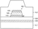
晶体管Tr1具有氧化物半导体层OS(OS1、OS2)、栅绝缘层GI1(第一栅绝缘层)及栅电极GL1(第一栅电极)。栅电极GL1与氧化物半导体层OS对置。栅绝缘层GI1设置在氧化物半导体层OS与栅电极GL1之间。在本实施方式中,例示了在比栅电极GL1靠基板SUB侧设置有氧化物半导体层OS的顶栅型晶体管,但也可以使用栅电极GL1与氧化物半导体层OS的位置关系相反的底栅型晶体管。The transistor Tr1 has an oxide semiconductor layer OS ( OS1 , OS2 ), a gate insulating layer GI1 (first gate insulating layer), and a gate electrode GL1 (first gate electrode). The gate electrode GL1 faces the oxide semiconductor layer OS. The gate insulating layer GI1 is provided between the oxide semiconductor layer OS and the gate electrode GL1. In this embodiment mode, a top-gate transistor in which the oxide semiconductor layer OS is provided on the substrate SUB side rather than the gate electrode GL1 is exemplified, but a bottom gate in which the positional relationship between the gate electrode GL1 and the oxide semiconductor layer OS is reversed may be used. type transistor.
氧化物半导体层OS包括氧化物半导体层OS1、OS2。氧化物半导体层OS1为在俯视时与栅电极GL1重叠的区域的氧化物半导体层。氧化物半导体层OS1作为半导体层发挥功能,并根据供给至栅电极GL1的电压而切换为导通状态与非导通状态。也就是说,氧化物半导体层OS1作为晶体管Tr1的通道发挥功能。氧化物半导体层OS2作为导电层发挥功能。氧化物半导体层OS1、OS2为由相同的氧化物半导体层形成的层。例如,氧化物半导体层OS2为通过对与氧化物半导体层OS1相同物性的层掺杂杂质而被低电阻化的氧化物半导体层。The oxide semiconductor layer OS includes oxide semiconductor layers OS1 and OS2. The oxide semiconductor layer OS1 is an oxide semiconductor layer in a region overlapping with the gate electrode GL1 in a plan view. The oxide semiconductor layer OS1 functions as a semiconductor layer, and is switched between a conductive state and a non-conductive state according to the voltage supplied to the gate electrode GL1. That is, the oxide semiconductor layer OS1 functions as a channel of the transistor Tr1. The oxide semiconductor layer OS2 functions as a conductive layer. The oxide semiconductor layers OS1 and OS2 are layers formed of the same oxide semiconductor layer. For example, the oxide semiconductor layer OS2 is an oxide semiconductor layer whose resistance is reduced by doping a layer having the same physical properties as the oxide semiconductor layer OS1 with impurities.
在栅电极GL1之上设置有绝缘层IL2。在绝缘层IL2之上设置有布线W1。布线W1经由设置于绝缘层IL2及栅绝缘层GI1的开口WCON而与氧化物半导体层OS2连接。与像素的灰度相关的数据信号被传递至布线W1。在绝缘层IL2及布线W1之上设置有绝缘层IL3。在绝缘层IL3之上设置有连接电极ZTCO。连接电极ZTCO经由设置于绝缘层IL3、IL2及栅绝缘层GI1的开口ZCON而与氧化物半导体层OS2连接。连接电极ZTCO在开口ZCON的底部与氧化物半导体层OS2接触。连接电极ZTCO为透明导电层。An insulating layer IL2 is provided on the gate electrode GL1. The wiring W1 is provided on the insulating layer IL2. The wiring W1 is connected to the oxide semiconductor layer OS2 through the opening WCON provided in the insulating layer IL2 and the gate insulating layer GI1. A data signal related to the gradation of the pixel is transferred to the wiring W1. An insulating layer IL3 is provided on the insulating layer IL2 and the wiring W1. A connection electrode ZTCO is provided on the insulating layer IL3. The connection electrode ZTCO is connected to the oxide semiconductor layer OS2 through the opening ZCON provided in the insulating layers IL3 and IL2 and the gate insulating layer GI1. The connection electrode ZTCO is in contact with the oxide semiconductor layer OS2 at the bottom of the opening ZCON. The connection electrode ZTCO is a transparent conductive layer.
将连接电极ZTCO与氧化物半导体层OS2接触的区域称为第一接触区域CON1。详细内容后文叙述,但连接电极ZTCO在俯视时不与栅电极GL1及布线W1重叠的第一接触区域CON1中与氧化物半导体层OS2接触。俯视时,第一接触区域CON1包括在像素的显示区域中。A region where the connection electrode ZTCO is in contact with the oxide semiconductor layer OS2 is referred to as a first contact region CON1. The details will be described later, but the connection electrode ZTCO is in contact with the oxide semiconductor layer OS2 in the first contact region CON1 that does not overlap the gate electrode GL1 and the wiring W1 in a plan view. When viewed from above, the first contact area CON1 is included in the display area of the pixel.
例如若将ITO层等透明导电层以与硅层等半导体层接触的方式而形成,则通过ITO成膜时的工艺气体、氧离子而使半导体层的表面氧化。形成于半导体层的表面的氧化层为高电阻,因此半导体层与透明导电层之间的接触电阻变高。其结果为,半导体层与透明导电层的电接触产生不良。另一方面,即使将上述的透明导电层以与氧化物半导体层接触的方式形成,在氧化物半导体层的表面也不形成上述那样的高电阻的氧化层。因此,氧化物半导体层与透明导电层之间的电接触不会产生不良。For example, when a transparent conductive layer such as an ITO layer is formed in contact with a semiconductor layer such as a silicon layer, the surface of the semiconductor layer is oxidized by the process gas and oxygen ions during ITO film formation. Since the oxide layer formed on the surface of the semiconductor layer has high resistance, the contact resistance between the semiconductor layer and the transparent conductive layer becomes high. As a result, poor electrical contact between the semiconductor layer and the transparent conductive layer occurs. On the other hand, even if the above-mentioned transparent conductive layer is formed in contact with the oxide semiconductor layer, the above-mentioned high-resistance oxide layer is not formed on the surface of the oxide semiconductor layer. Therefore, the electrical contact between the oxide semiconductor layer and the transparent conductive layer does not become defective.
在连接电极ZTCO之上设置有绝缘层IL4。绝缘层IL4缓和由设置在比绝缘层IL4靠下层的结构体形成的高低差。有时将绝缘层IL4称为平坦化膜。在绝缘层IL4之上设置有像素电极PTCO。像素电极PTCO经由设置于绝缘层IL4的开口PCON而与连接电极ZTCO连接。将连接电极ZTCO与像素电极PTCO接触的区域称为第二接触区域CON2。俯视时,第二接触区域CON2与栅电极GL1重叠。像素电极PTCO为透明导电层。An insulating layer IL4 is provided on the connection electrode ZTCO. The insulating layer IL4 relieves the level difference formed by the structure provided in the lower layer than the insulating layer IL4. The insulating layer IL4 is sometimes referred to as a planarizing film. A pixel electrode PTCO is provided on the insulating layer IL4. The pixel electrode PTCO is connected to the connection electrode ZTCO through the opening PCON provided in the insulating layer IL4. A region where the connection electrode ZTCO is in contact with the pixel electrode PTCO is referred to as a second contact region CON2. In a plan view, the second contact region CON2 overlaps with the gate electrode GL1. The pixel electrode PTCO is a transparent conductive layer.
在像素电极PTCO之上设置有绝缘层IL5。在绝缘层IL5之上设置有公共辅助电极CMTL及公共电极CTCO。即,像素电极PTCO经由绝缘层IL5而与公共电极CTCO对置。公共电极CTCO在开口PCON(第二接触区域CON2内)与公共辅助电极CMTL连接。详细内容后文叙述,但公共辅助电极CMTL与公共电极CTCO具有分别不同的平面图案。公共辅助电极CMTL为金属层。公共电极CTCO为透明导电层。公共辅助电极CMTL的电阻与公共电极CTCO的电阻相比为低电阻。公共辅助电极CMTL也作为遮光层发挥功能。例如,通过公共辅助电极CMTL对来自邻接的像素的光进行遮光,从而抑制了混色的产生。在公共电极CTCO之上设置有隔离件SP。An insulating layer IL5 is provided on the pixel electrode PTCO. A common auxiliary electrode CMTL and a common electrode CTCO are arranged on the insulating layer IL5. That is, the pixel electrode PTCO faces the common electrode CTCO via the insulating layer IL5. The common electrode CTCO is connected to the common auxiliary electrode CMTL in the opening PCON (in the second contact region CON2). The details will be described later, but the common auxiliary electrode CMTL and the common electrode CTCO have different plane patterns, respectively. The common auxiliary electrode CMTL is a metal layer. The common electrode CTCO is a transparent conductive layer. The resistance of the common auxiliary electrode CMTL is low in resistance compared to the resistance of the common electrode CTCO. The common auxiliary electrode CMTL also functions as a light shielding layer. For example, light from adjacent pixels is shielded by the common auxiliary electrode CMTL, thereby suppressing the occurrence of color mixing. A spacer SP is provided over the common electrode CTCO.
隔离件SP针对一部分的像素而设置。例如,隔离件SP可以针对蓝色像素、红色像素、绿色像素中的任一个像素而设置。不过,隔离件SP也可以设置于所有像素。隔离件SP的高度为单元间隙的一半的高度。在对置基板也设置有隔离件,对置基板的隔离件与上述的隔离件SP在俯视时重叠。The spacers SP are provided for some of the pixels. For example, the spacer SP may be provided for any one of blue pixels, red pixels, and green pixels. However, the spacers SP may be provided in all the pixels. The height of the spacer SP is half the height of the cell gap. A spacer is also provided on the opposing substrate, and the spacer of the opposing substrate overlaps the above-described spacer SP in a plan view.
在晶体管Tr1与基板SUB之间设置有遮光层LS。在本实施方式中,作为遮光层LS,设置有遮光层LS1、LS2。不过,遮光层LS也可以仅由遮光层LS1或LS2形成。在俯视时,遮光层LS设置于栅电极GL1与氧化物半导体层OS重叠的区域。即,在俯视时,遮光层LS设置于与氧化物半导体层OS1重叠的区域。遮光层LS抑制从基板SUB侧入射的光到达氧化物半导体层OS1。在作为遮光层LS使用导电层的情况下,也可以对遮光层LS施加电压而控制氧化物半导体层OS1。在对遮光层LS施加电压的情况下,遮光层LS与栅电极GL1也可以在像素电路的周边区域连接。在俯视时,上述的第一接触区域CON1设置于不与遮光层LS重叠的区域。A light shielding layer LS is provided between the transistor Tr1 and the substrate SUB. In this embodiment, the light-shielding layers LS1 and LS2 are provided as the light-shielding layer LS. However, the light shielding layer LS may be formed of only the light shielding layer LS1 or LS2. The light shielding layer LS is provided in a region where the gate electrode GL1 and the oxide semiconductor layer OS overlap with each other in a plan view. That is, in a plan view, the light shielding layer LS is provided in a region overlapping with the oxide semiconductor layer OS1. The light shielding layer LS suppresses light incident from the substrate SUB side from reaching the oxide semiconductor layer OS1. When a conductive layer is used as the light shielding layer LS, the oxide semiconductor layer OS1 may be controlled by applying a voltage to the light shielding layer LS. When a voltage is applied to the light shielding layer LS, the light shielding layer LS and the gate electrode GL1 may be connected in the peripheral region of the pixel circuit. In a plan view, the above-described first contact region CON1 is provided in a region that does not overlap with the light shielding layer LS.
[1-3.晶体管Tr2的构成][1-3. Configuration of transistor Tr2]
晶体管Tr2具有p型的晶体管Tr2-1和n型的晶体管Tr2-2。有时将晶体管Tr2称为“第二晶体管”。The transistor Tr2 includes a p-type transistor Tr2-1 and an n-type transistor Tr2-2. The transistor Tr2 is sometimes referred to as a "second transistor".
p型的晶体管Tr2-1和n型的晶体管Tr2-2均具有栅电极GL2、栅绝缘层GI2、半导体层S(S1、S2、S3)。栅电极GL2与半导体层S对置。栅绝缘层GI2设置在半导体层S与栅电极GL2之间。在本实施方式中,例示了在比半导体层S靠基板SUB侧设置有栅电极GL2的底栅型晶体管,但也可以使用半导体层S与栅电极GL2的位置关系相反的顶栅型晶体管。有时将栅电极GL2称为“第二栅电极”。有时将栅绝缘层GI2称为“第二栅绝缘层”。Both the p-type transistor Tr2-1 and the n-type transistor Tr2-2 have a gate electrode GL2, a gate insulating layer GI2, and a semiconductor layer S (S1, S2, S3). The gate electrode GL2 is opposed to the semiconductor layer S. The gate insulating layer GI2 is provided between the semiconductor layer S and the gate electrode GL2. In this embodiment, a bottom-gate transistor in which the gate electrode GL2 is provided on the substrate SUB side rather than the semiconductor layer S is exemplified, but a top-gate transistor in which the positional relationship between the semiconductor layer S and the gate electrode GL2 is reversed may be used. The gate electrode GL2 is sometimes referred to as a "second gate electrode". The gate insulating layer GI2 is sometimes referred to as a "second gate insulating layer".
p型的晶体管Tr2-1的半导体层S包括半导体层S1、S2。n型的晶体管Tr2-2的半导体层S包括半导体层S1、S2、S3。半导体层S1为在俯视时与栅电极GL2重叠的区域的半导体层。半导体层S1作为晶体管Tr2-1和Tr2-2的通道发挥功能。半导体层S2作为导电层发挥功能。半导体层S3作为电阻比半导体层S2高的导电层发挥功能。半导体层S3通过使朝向半导体层S1侵入的热载流子衰减,从而抑制热载流子劣化。The semiconductor layer S of the p-type transistor Tr2-1 includes semiconductor layers S1 and S2. The semiconductor layer S of the n-type transistor Tr2-2 includes semiconductor layers S1, S2, and S3. The semiconductor layer S1 is a semiconductor layer in a region overlapping with the gate electrode GL2 in plan view. The semiconductor layer S1 functions as a channel for the transistors Tr2-1 and Tr2-2. The semiconductor layer S2 functions as a conductive layer. The semiconductor layer S3 functions as a conductive layer having a higher resistance than the semiconductor layer S2. The semiconductor layer S3 attenuates hot carriers that have penetrated toward the semiconductor layer S1, thereby suppressing hot carrier degradation.
在半导体层S之上设置有绝缘层IL1及栅绝缘层GI1。在晶体管Tr2中,栅绝缘层GI1仅作为层间膜(第一绝缘层)发挥功能。即,第一绝缘层覆盖晶体管Tr2。在该情况下,第一绝缘层与栅绝缘层GI1为同一层。在这些绝缘层之上设置有布线W2。布线W2经由设置于绝缘层IL1及栅绝缘层GI1的开口而与半导体层S连接。在布线W2之上设置有绝缘层IL2。在绝缘层IL2之上设置有布线W1。布线W1经由设置于绝缘层IL2的开口而与布线W2连接。On the semiconductor layer S, an insulating layer IL1 and a gate insulating layer GI1 are provided. In the transistor Tr2, the gate insulating layer GI1 functions only as an interlayer film (first insulating layer). That is, the first insulating layer covers the transistor Tr2. In this case, the first insulating layer and the gate insulating layer GI1 are the same layer. Wiring W2 is provided over these insulating layers. The wiring W2 is connected to the semiconductor layer S through openings provided in the insulating layer IL1 and the gate insulating layer GI1. An insulating layer IL2 is provided on the wiring W2. The wiring W1 is provided on the insulating layer IL2. The wiring W1 is connected to the wiring W2 through an opening provided in the insulating layer IL2.
如图1A所示,设置于周边电路的栅电极GL2与设置于像素电路的遮光层LS2为同一层。设置于周边电路的布线W2(第一周边电路布线)与设置于像素电路的栅电极GL1(第一栅电极)为同一层。在周边电路中,布线W2经由贯通绝缘层(栅绝缘层GI1、缘层IL1、栅绝缘层GI2)而设置的接触孔与和栅电极GL2设置在同一层的布线W3(第二周边电路布线)连接。同一层意味着通过将一个层图案化而形成多个部件、或者通过对相同的单层材料或者层叠材料进行图案化而在同一工序同时形成的层。即,栅电极GL1的各层的厚度及各层的锥角与布线W2的各层的厚度及各层的锥角实际上相同。As shown in FIG. 1A , the gate electrode GL2 provided in the peripheral circuit and the light shielding layer LS2 provided in the pixel circuit are the same layer. The wiring W2 (first peripheral circuit wiring) provided in the peripheral circuit and the gate electrode GL1 (first gate electrode) provided in the pixel circuit are in the same layer. In the peripheral circuit, the wiring W2 and the wiring W3 (second peripheral circuit wiring) provided on the same layer as the gate electrode GL2 via a contact hole provided through the insulating layers (gate insulating layer GI1, edge layer IL1, gate insulating layer GI2) connect. The same layer means a layer formed simultaneously in the same process by patterning one layer to form a plurality of components, or by patterning the same single-layer material or laminated material. That is, the thickness of each layer of the gate electrode GL1 and the taper angle of each layer are substantially the same as the thickness of each layer of the wiring W2 and the taper angle of each layer.
[1-4.栅电极GL1的构成][1-4. Configuration of gate electrode GL1 ]
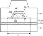
使用图1B对栅电极GL1的详细截面构成进行说明。如图1B所示,栅电极GL1具有第一导电层110、第二导电层120及第三导电层130。第一导电层110设置在栅绝缘层GI1之上,并与栅绝缘层GI1接触。第二导电层120设置在第一导电层110之上,并与第一导电层110接触。第三导电层130设置在第二导电层120之上,并与第二导电层120接触。The detailed cross-sectional configuration of the gate electrode GL1 will be described with reference to FIG. 1B . As shown in FIG. 1B , the gate electrode GL1 has a first
第一导电层110、第二导电层120及第三导电层130各自的侧部具有倾斜面朝向上方的锥形形状。在图1B中,将上述倾斜面与栅绝缘层GI1(或者,基板SUB的上表面或水平面)所成的角称为锥角θ。在图1B中,示出了这些导电层的侧面存在于直线上的锥形形状,但并不限于该构成。例如,这些导电层的侧面的倾斜角也可以分别不同。第一导电层110的侧面的上端与第二导电层120的侧面的下端也可以不一致。同样地,第二导电层120的侧面的上端与第三导电层130的侧面的下端也可以不一致。例如,第一导电层110的上表面的一部分也可以从第二导电层120露出。同样地,第二导电层120的上表面的一部也可以从第三导电层130露出。Each side portion of the first
作为第一导电层110及第三导电层130,使用具备氢吸留性的材料。换言之,作为第一导电层110及第三导电层130,使用能够在其表面形成金属氢化物的材料。具体地,作为第一导电层110及第三导电层130,使用钛(Ti)、镁(Mg)、钒(V)、镧(La)、以及含有它们的合金。例如,在作为第一导电层110及第三导电层130使用了Ti的情况下,通过Ti吸收制造工序中的水分及酸性液中所含有的氢,从而形成金属氢化物(TiH2)。像这样,通过Ti等上述的材料形成氢化物,从而第一导电层110及第三导电层130具备氢吸留性。As the first
作为第二导电层120,使用电阻比第一导电层110及第三导电层130小的材料。例如,使用铝(Al)、钼(Mo)、钨(W)、银(Ag)及含有它们的合金(例如,钼与钨的合金)作为第二导电层120。As the second
[1-5.显示装置10的平面布局][1-5. Plane Layout of Display Device 10 ]
使用图2~图13对显示装置10的像素的平面布局进行说明。在图2中,省略了像素电极PTCO、公共辅助电极CMTL、公共电极CTCO以及隔离件SP。像素电极PTCO、公共辅助电极CMTL以及公共电极CTCO的平面布局分别在图11~图13中示出。The plane layout of the pixels of the
如图2和图3所示,遮光层LS沿D1方向延伸。通过像素而使遮光层LS的形状不同。在本实施方式中,设置有从沿D1方向延伸的遮光层LS的一部分向D2方向突出的突出部PJT。如图5所示,遮光层LS设置于包括在俯视时栅电极GL1与氧化物半导体层OS重叠的区域的区域。此外,也能够将栅电极GL1称为“栅极线”。As shown in FIGS. 2 and 3 , the light shielding layer LS extends in the D1 direction. The shape of the light shielding layer LS is varied by the pixels. In the present embodiment, a protruding portion PJT that protrudes in the D2 direction from a part of the light shielding layer LS extending in the D1 direction is provided. As shown in FIG. 5 , the light shielding layer LS is provided in a region including a region where the gate electrode GL1 and the oxide semiconductor layer OS overlap with each other in plan view. In addition, the gate electrode GL1 can also be called a "gate line".
如图2、图4及图5所示,氧化物半导体层OS沿D2方向延伸。栅电极GL1以与氧化物半导体层OS交叉的方式沿D1方向延伸。栅电极GL1的图案设置在遮光层LS的图案的内侧。换言之,氧化物半导体层OS形成为与栅电极GL1交叉的长条状。As shown in FIGS. 2 , 4 and 5 , the oxide semiconductor layer OS extends in the D2 direction. The gate electrode GL1 extends in the D1 direction so as to intersect the oxide semiconductor layer OS. The pattern of the gate electrode GL1 is provided inside the pattern of the light shielding layer LS. In other words, the oxide semiconductor layer OS is formed in a long shape intersecting with the gate electrode GL1.
如图2、图6及图7所示,开口WCON在氧化物半导体层OS的图案的上端附近,设置于与布线W1重叠的区域。氧化物半导体层OS的图案的主要部分在邻接的布线W1之间沿D2方向延伸。氧化物半导体层OS的图案的剩余部分从该主要部分朝向开口WCON的区域沿相对于D1方向及D2方向倾斜的方向延伸。As shown in FIG. 2 , FIG. 6 , and FIG. 7 , the opening WCON is provided in the region overlapping the wiring W1 in the vicinity of the upper end of the pattern of the oxide semiconductor layer OS. The main part of the pattern of the oxide semiconductor layer OS extends in the D2 direction between the adjacent wirings W1. The remainder of the pattern of the oxide semiconductor layer OS extends from the main portion toward the region of the opening WCON in directions inclined with respect to the D1 direction and the D2 direction.
如图2及图7所示,多个布线W1沿D2方向延伸。在需要分别区分邻接的布线W1来进行说明的情况下,将邻接的布线W1称为布线W1-1(第一像素布线)及布线W1-2(第二像素布线)。在该情况下,氧化物半导体层OS的主要部分能够在第一像素布线W1-1与第二像素布线W1-2之间沿D2方向延伸,并与栅电极GL1交叉。将上述的构成换句话说,氧化物半导体层OS在D2方向上设置成长条状(具有长边的形状),并通过氧化物半导体层OS的长边方向的一个端部与布线W1-1连接。As shown in FIGS. 2 and 7 , the plurality of wirings W1 extend in the D2 direction. When it is necessary to distinguish and describe the adjacent wirings W1, the adjacent wirings W1 are referred to as wirings W1-1 (first pixel wirings) and wirings W1-2 (second pixel wirings). In this case, the main portion of the oxide semiconductor layer OS can extend in the D2 direction between the first pixel wiring W1-1 and the second pixel wiring W1-2, and intersect the gate electrode GL1. In other words, the oxide semiconductor layer OS is formed in a strip shape (having a long side shape) in the D2 direction, and the oxide semiconductor layer OS is connected to the wiring W1-1 through one end portion in the long side direction of the oxide semiconductor layer OS. .
如图2、图8及图9所示,开口ZCON设置在氧化物半导体层OS的图案的下端附近。开口ZCON设置于与氧化物半导体层OS的图案重叠的区域、且不与栅电极GL1重叠的区域。开口ZCON设置于与连接电极ZTCO重叠的区域。连接电极ZTCO在布线W1-1与布线W1-2之间,与栅电极GL1及氧化物半导体层OS重叠。由此,连接电极ZTCO在不与栅电极GL1重叠的开口ZCON(第一接触区域CON1)与氧化物半导体层OS接触。As shown in FIGS. 2 , 8 and 9 , the opening ZCON is provided in the vicinity of the lower end of the pattern of the oxide semiconductor layer OS. The opening ZCON is provided in a region overlapping with the pattern of the oxide semiconductor layer OS and not overlapping with the gate electrode GL1. The opening ZCON is provided in a region overlapping with the connection electrode ZTCO. The connection electrode ZTCO overlaps the gate electrode GL1 and the oxide semiconductor layer OS between the wiring W1-1 and the wiring W1-2. Thereby, the connection electrode ZTCO is brought into contact with the oxide semiconductor layer OS at the opening ZCON (first contact region CON1) not overlapping with the gate electrode GL1.
将上述的构成换句话说,氧化物半导体层OS通过氧化物半导体层OS的长边方向的另一端部与连接电极ZTCO(第一透明导电层)连接。连接电极ZTCO(第一透明导电层)与氧化物半导体层OS同样地形成为沿D2方向延伸的长条状。在D1方向上,连接电极ZTCO(第一透明导电层)的宽度比氧化物半导体层OS的宽度小。In other words, the above-described configuration is such that the oxide semiconductor layer OS is connected to the connection electrode ZTCO (first transparent conductive layer) through the other end portion in the longitudinal direction of the oxide semiconductor layer OS. The connection electrode ZTCO (first transparent conductive layer) is formed in a long strip shape extending in the D2 direction similarly to the oxide semiconductor layer OS. In the D1 direction, the width of the connection electrode ZTCO (first transparent conductive layer) is smaller than the width of the oxide semiconductor layer OS.
如图2、图7及图8所示,氧化物半导体层OS相对于栅电极GL1在与开口ZCON(第一接触区域CON1)相反的一侧与布线W1接触。开口ZCON(第一接触区域CON1)不与遮光层LS重叠。As shown in FIGS. 2 , 7 and 8 , the oxide semiconductor layer OS is in contact with the wiring W1 on the side opposite to the opening ZCON (first contact region CON1 ) with respect to the gate electrode GL1 . The opening ZCON (the first contact region CON1 ) does not overlap with the light shielding layer LS.
如图2、图10及图11所示,开口PCON设置在连接电极ZTCO的图案的上端附近。开口PCON设置于与栅电极GL1的图案及连接电极ZTCO的图案重叠的区域。开口PCON设置于与像素电极PTCO重叠的区域。像素电极PTCO在布线W1-1与布线W1-2之间,与栅电极GL1、氧化物半导体层OS及连接电极ZTCO重叠。由此,像素电极PTCO在与栅电极GL1重叠的开口PCON(第二接触区域CON2)与连接电极ZTCO接触。As shown in FIGS. 2 , 10 and 11 , the opening PCON is provided in the vicinity of the upper end of the pattern of the connection electrode ZTCO. The opening PCON is provided in a region overlapping with the pattern of the gate electrode GL1 and the pattern of the connection electrode ZTCO. The opening PCON is disposed in a region overlapping with the pixel electrode PTCO. The pixel electrode PTCO overlaps with the gate electrode GL1, the oxide semiconductor layer OS, and the connection electrode ZTCO between the wiring W1-1 and the wiring W1-2. Thereby, the pixel electrode PTCO is brought into contact with the connection electrode ZTCO at the opening PCON (second contact region CON2) overlapping with the gate electrode GL1.
像素电极PTCO在下述的透光区域延伸。有时将像素电极PTCO称为“第二透明导电层”。若将上述的构成换句话说,像素电极PTCO(第二透明导电层)与氧化物半导体层OS及布线W1-1(第一像素布线)同样地,形成为沿D2方向延伸的长条状。在D1方向上,设置了开口PCON的部分中的像素电极PTCO(第二透明导电层)的宽度比氧化物半导体层OS的宽度大。The pixel electrode PTCO extends in a light-transmitting region described below. The pixel electrode PTCO is sometimes referred to as the "second transparent conductive layer". In other words, the pixel electrode PTCO (second transparent conductive layer) is formed in an elongated shape extending in the D2 direction, similarly to the oxide semiconductor layer OS and the wiring W1-1 (first pixel wiring). In the D1 direction, the width of the pixel electrode PTCO (second transparent conductive layer) in the portion where the opening PCON is provided is larger than the width of the oxide semiconductor layer OS.
如图11所示,连接电极ZTCO(第一透明导电层)形成为沿着布线W1-1(第一像素布线)延伸的长条状。在D1方向上,构成第二接触区域CON2的开口PCON的宽度比连接电极ZTCO(第一透明导电层)的宽度大。在俯视时连接电极ZTCO(第一透明导电层)的整体与像素电极PTCO(第二透明导电层)重叠。As shown in FIG. 11 , the connection electrode ZTCO (first transparent conductive layer) is formed in an elongated shape extending along the wiring W1-1 (first pixel wiring). In the D1 direction, the width of the opening PCON constituting the second contact region CON2 is larger than the width of the connection electrode ZTCO (first transparent conductive layer). The entire connection electrode ZTCO (first transparent conductive layer) overlaps with the pixel electrode PTCO (second transparent conductive layer) in a plan view.
如图11所示,像素电极PTCO沿D2方向排列。有时将沿D2方向邻接的像素中的、一方的像素称为“第一像素”,将另一方的像素称为“第二像素”。例如,第一像素为与在图11中沿D2方向排列的像素电极PTCO中的上方的像素电极PTCO对应的像素,第二像素为与沿D2方向排列的像素电极PTCO中的下方的像素电极PTCO对应的像素。在该情况下,从布线W1-1(第一像素布线)对第一像素及第二像素供给像素信号。As shown in FIG. 11 , the pixel electrodes PTCO are arranged in the D2 direction. Among the pixels adjacent in the D2 direction, one pixel may be referred to as a "first pixel", and the other pixel may be referred to as a "second pixel". For example, the first pixel is a pixel corresponding to the upper pixel electrode PTCO among the pixel electrodes PTCO arranged along the D2 direction in FIG. 11 , and the second pixel is the pixel electrode PTCO lower than the pixel electrodes PTCO arranged along the D2 direction. corresponding pixel. In this case, pixel signals are supplied from the wiring W1-1 (first pixel wiring) to the first pixel and the second pixel.
另外,像素电极PTCO沿D1方向排列。将相对于上述的第一像素在D1方向上邻接的像素称为“第三像素”,将相对于第二像素在D1方向上邻接的像素称为“第四像素”。第三像素与第四像素在D2方向上邻接。从与布线W1-1(第一像素布线)相邻的布线W1-2(第二像素布线)对第三像素及第四像素供给像素信号。In addition, the pixel electrodes PTCO are arranged in the D1 direction. The pixel adjacent to the above-described first pixel in the D1 direction is referred to as a “third pixel”, and the pixel adjacent to the second pixel in the D1 direction is referred to as a “fourth pixel”. The third pixel is adjacent to the fourth pixel in the D2 direction. The third pixel and the fourth pixel are supplied with pixel signals from the wiring W1-2 (second pixel wiring) adjacent to the wiring W1-1 (first pixel wiring).
如上述那样,第一像素、第二像素、第三像素及第四像素分别具有晶体管Tr1(像素晶体管)、连接电极ZTCO(第一透明导电层)及像素电极PTCO(第二透明导电层)。As described above, the first pixel, the second pixel, the third pixel, and the fourth pixel have the transistor Tr1 (pixel transistor), the connection electrode ZTCO (first transparent conductive layer), and the pixel electrode PTCO (second transparent conductive layer), respectively.
晶体管Tr1具备氧化物半导体层OS、与氧化物半导体层OS对置的栅电极GL1、以及氧化物半导体层OS与栅电极GL1之间的栅绝缘层GI1。连接电极ZTCO在俯视时与栅电极GL1及氧化物半导体层OS重叠,并在不与栅电极GL1重叠的开口ZCON(第一接触区域CON1)与氧化物半导体层OS接触。像素电极PTCO在俯视时与栅电极GL1、氧化物半导体层OS及连接电极ZTCO重叠,并在与栅电极GL1重叠的开口PCON(第二接触区域CON2)与连接电极ZTCO连接。The transistor Tr1 includes an oxide semiconductor layer OS, a gate electrode GL1 facing the oxide semiconductor layer OS, and a gate insulating layer GI1 between the oxide semiconductor layer OS and the gate electrode GL1. The connection electrode ZTCO overlaps the gate electrode GL1 and the oxide semiconductor layer OS in plan view, and is in contact with the oxide semiconductor layer OS at the opening ZCON (first contact region CON1 ) that does not overlap the gate electrode GL1 . The pixel electrode PTCO overlaps the gate electrode GL1 , the oxide semiconductor layer OS, and the connection electrode ZTCO in plan view, and is connected to the connection electrode ZTCO at the opening PCON (second contact region CON2 ) overlapping the gate electrode GL1 .
图11的上侧设置的第一像素的像素电极PTCO在俯视时与该第一像素的氧化物半导体层OS及设置在第一像素的下侧的第二像素的氧化物半导体层OS重叠。另外,第一像素的像素电极PTCO在俯视时也与第四像素的氧化物半导体层OS重叠。The pixel electrode PTCO of the first pixel provided on the upper side of FIG. 11 overlaps the oxide semiconductor layer OS of the first pixel and the oxide semiconductor layer OS of the second pixel provided below the first pixel in plan view. In addition, the pixel electrode PTCO of the first pixel also overlaps with the oxide semiconductor layer OS of the fourth pixel in plan view.
如图12所示,公共辅助电极CMTL以包围像素区域的周围的方式设置成格子状。即,公共辅助电极CMTL相对于多个像素共用地设置。换言之,公共辅助电极CMTL具有开口OP。开口OP设置为将像素电极PTCO露出。开口OP的图案设置在像素电极PTCO的图案的内侧。设置有开口OP的区域相当于显示区域。即,开口ZCON(第一接触区域CON1)包括在显示区域中。显示区域意味着用户能够视觉确认来自像素的光的区域。例如,被金属层遮光、用户无法视觉确认光的区域不包括在显示区域中。即,有时将上述的显示区域称为“透光区域(或者,开口区域)”。As shown in FIG. 12 , the common auxiliary electrodes CMTL are arranged in a lattice shape so as to surround the periphery of the pixel region. That is, the common auxiliary electrode CMTL is provided in common with a plurality of pixels. In other words, the common auxiliary electrode CMTL has the opening OP. The opening OP is provided to expose the pixel electrode PTCO. The pattern of openings OP is provided inside the pattern of the pixel electrode PTCO. The area where the opening OP is provided corresponds to the display area. That is, the opening ZCON (the first contact area CON1 ) is included in the display area. The display area means the area where the user can visually recognize the light from the pixel. For example, an area blocked by the metal layer and the user cannot visually confirm the light is not included in the display area. That is, the above-mentioned display area may be referred to as a "light-transmitting area (or an opening area)" in some cases.
如图13所示,公共电极CTCO相对于多个像素共用地设置。在与上述开口OP对应的区域设置有狭缝SL。狭缝SL具有弯曲的形状(纵长的S字形状)。狭缝SL的前端具有与该前端的延伸方向正交的宽度变小的形状。参照图1及图13,公共电极CTCO在与像素电极PTCO(第二透明导电层)对置的位置具有狭缝SL。As shown in FIG. 13 , the common electrode CTCO is provided in common with a plurality of pixels. The slit SL is provided in the area|region corresponding to the said opening OP. The slit SL has a curved shape (longitudinal S-shape). The front end of the slit SL has a shape with a reduced width perpendicular to the extending direction of the front end. 1 and 13 , the common electrode CTCO has a slit SL at a position opposite to the pixel electrode PTCO (second transparent conductive layer).
[1-6.显示装置10的各部件的材质][1-6. Materials of Components of Display Device 10 ]
作为基板SUB,能够使用玻璃基板、石英基板及蓝宝石基板等具有透光性、且不具有挠性的刚性基板。另一方面,在需要基板SUB具有挠性的情况下,作为基板SUB,能够使用聚酰亚胺基板、丙烯酸基板、硅氧烷基板、或者氟树脂基板等含有树脂、且具有挠性的柔性基板。为了提高基板SUB的耐热性,也可以向上述的树脂导入杂质。As the substrate SUB, a glass substrate, a quartz substrate, and a sapphire substrate can be used as a rigid substrate having light transmittance and not having flexibility. On the other hand, when the substrate SUB is required to have flexibility, a flexible substrate containing a resin such as a polyimide substrate, an acrylic substrate, a silicone substrate, or a fluororesin substrate can be used as the substrate SUB. . In order to improve the heat resistance of the substrate SUB, impurities may be introduced into the above-mentioned resin.
作为栅电极GL2、布线W1、W2、遮光层LS及公共辅助电极CMTL,能够使用普通的金属材料。例如,作为它们的电极等部件,使用铝(Al)、钛(Ti)、铬(Cr)、钴(Co)、镍(Ni)、钼(Mo)、铪(Hf)、钽(Ta)、钨(W)、铋(Bi)及银(Ag)、或者它们的合金或化合物。作为上述的电极等部件,可以单层地使用上述的材料,也可以层叠地使用上述的材料。Common metal materials can be used as the gate electrode GL2, the wirings W1, W2, the light shielding layer LS, and the common auxiliary electrode CMTL. For example, aluminum (Al), titanium (Ti), chromium (Cr), cobalt (Co), nickel (Ni), molybdenum (Mo), hafnium (Hf), tantalum (Ta), Tungsten (W), bismuth (Bi), silver (Ag), or their alloys or compounds. As the members such as the above-mentioned electrodes, the above-mentioned materials may be used in a single layer, or may be used in a stacked layer.
作为栅绝缘层GI1、GI2及绝缘层IL1~IL5,能够使用通常的绝缘层性材料。例如,作为绝缘层IL1~IL3、IL5,能够使用氧化硅(SiOx)、氧化氮化硅(SiOxNy)、氮化硅(SiNx)、氮化氧化硅(SiNxOy)、氧化铝(AlOx)、氧化氮化铝(AlOxNy)、氮化氧化铝(AlNxOy)、氮化铝(AlNx)等无机绝缘层。作为这些绝缘层,能够使用缺陷少的绝缘层。作为绝缘层IL4,能够使用聚酰亚胺树脂、丙烯酸树脂、环氧树脂、硅酮树脂、氟树脂、或者硅氧烷树脂等有机绝缘材料。作为栅绝缘层GI1、GI2及绝缘层IL1~IL3、IL5,也可以使用上述的有机绝缘材料。作为上述的绝缘层等的部件,可以单层地使用上述的材料,也可以层叠地使用。As the gate insulating layers GI1 and GI2 and the insulating layers IL1 to IL5, common insulating layer materials can be used. For example, as the insulating layers IL1 to IL3 and IL5, silicon oxide (SiOx ), silicon nitride oxide (SiOx Ny ), silicon nitride (SiNx ), silicon nitride oxide (SiNx Oy ), Inorganic insulating layers such as aluminum oxide (AlOx ), aluminum oxide nitride (AlOx Ny ), aluminum nitride (AlNx Oy ), and aluminum nitride (AlNx ). As these insulating layers, insulating layers with few defects can be used. As the insulating layer IL4, an organic insulating material such as polyimide resin, acrylic resin, epoxy resin, silicone resin, fluororesin, or siloxane resin can be used. As the gate insulating layers GI1 and GI2 and the insulating layers IL1 to IL3 and IL5, the above-mentioned organic insulating materials can also be used. As the members such as the above-mentioned insulating layers, the above-mentioned materials may be used in a single layer, or may be used in a laminated form.
作为上述的绝缘层的一个例子,作为栅绝缘层GI1使用厚度为100nm的SiOx。作为绝缘层IL1使用总厚度为600nm~700nm的SiOx/SiNx/SiOx。作为栅绝缘层GI2使用总厚度为60~100nm的SiOx/SiNx。作为绝缘层IL2使用总厚度为300nm~500nm的SiOx/SiNx/SiOx。作为绝缘层IL3使用总厚度为200nm~500nm的SiOx(单层)、SiNx(单层)、或者它们的叠层。作为绝缘层IL4使用厚度为2μm~4μm的有机层。作为绝缘层IL5使用厚度为50nm~150nm的SiNx(单层)。As an example of the above-described insulating layer, SiOx having a thickness of 100 nm is used as the gate insulating layer GI1. As the insulating layer IL1, SiOx /SiNx /SiOx having a total thickness of 600 nm to 700 nm is used. As the gate insulating layer GI2, SiOx /SiNx having a total thickness of 60 to 100 nm is used. As the insulating layer IL2, SiOx /SiNx /SiOx having a total thickness of 300 nm to 500 nm is used. As the insulating layer IL3, SiOx (single layer), SiNx (single layer), or a stacked layer thereof having a total thickness of 200 nm to 500 nm is used. As the insulating layer IL4, an organic layer having a thickness of 2 μm to 4 μm is used. As the insulating layer IL5, SiNx (single layer) having a thickness of 50 nm to 150 nm is used.
上述的SiOxNy及AlOxNy为含有比氧(O)小的比率(x>y)的氮(N)的硅化合物及铝化合物。SiNxOy及AlNxOy为含有比氮小的比率(x>y)的氧的硅化合物及铝化合物。The above-mentioned SiOx Ny and AlOx Ny are silicon compounds and aluminum compounds containing nitrogen (N) in a ratio (x>y) smaller than oxygen (O). SiNx Oy and AlNx Oy are silicon compounds and aluminum compounds containing oxygen in a ratio (x>y) smaller than nitrogen.
作为氧化物半导体层OS,能够使用具有半导体的特性的氧化金属。氧化物半导体层OS具有透光性。例如,能够使用含有铟(In)、镓(Ga)、锌(Zn)及氧(O)的氧化物半导体作为氧化物半导体层OS。特别是,能够使用具有In:Ga:Zn:O=1:1:1:4的组成比的氧化物半导体。不过,本实施方式中使用的含有In、Ga、Zn及O的氧化物半导体并不限于上述的组成,也能够使用与上述不同的组成的氧化物半导体。例如,为了提高移动度,也可以使In的比率比上述大。另外,为了增大带隙并减小基于光照射的影响,也可以使Ga的比率比上述大。As the oxide semiconductor layer OS, a metal oxide having semiconductor characteristics can be used. The oxide semiconductor layer OS has light transmittance. For example, an oxide semiconductor containing indium (In), gallium (Ga), zinc (Zn), and oxygen (O) can be used as the oxide semiconductor layer OS. In particular, an oxide semiconductor having a composition ratio of In:Ga:Zn:O=1:1:1:4 can be used. However, the oxide semiconductor containing In, Ga, Zn, and O used in the present embodiment is not limited to the above-mentioned composition, and an oxide semiconductor of a composition different from the above-mentioned composition may be used. For example, in order to improve the mobility, the ratio of In may be made larger than the above. In addition, in order to increase the band gap and reduce the influence due to light irradiation, the ratio of Ga may be made larger than the above.
也可以对含有In、Ga、Zn及O的氧化物半导体添加其他元素。例如,可以对该氧化物半导体添加Al、Sn等金属元素。除上述的氧化物半导体以外,也可以使用含有In和Ga的氧化物半导体(IGO)、含有In和Zn的氧化物半导体(IZO)、含有In、Sn及Zn的氧化物半导体(ITZO)、以及含有In和W的氧化物半导体等作为氧化物半导体层OS。氧化物半导体层OS既可以是非晶态,也可以是结晶性。氧化物半导体层OS也可以是非晶态与结晶的混相。Other elements may be added to the oxide semiconductor containing In, Ga, Zn, and O. For example, a metal element such as Al and Sn may be added to the oxide semiconductor. In addition to the above oxide semiconductors, oxide semiconductors containing In and Ga (IGO), oxide semiconductors containing In and Zn (IZO), oxide semiconductors containing In, Sn and Zn (ITZO), and An oxide semiconductor or the like containing In and W is used as the oxide semiconductor layer OS. The oxide semiconductor layer OS may be amorphous or crystalline. The oxide semiconductor layer OS may be a mixed phase of amorphous and crystalline.
作为连接电极ZTCO、像素电极PTCO及公共电极CTCO,使用透明导电层。作为该透明导电层,能够使用氧化铟与氧化锡的混合物(ITO)及氧化铟与氧化锌的混合物(IZO)。作为该透明导电层,也可以使用除上述以外的材料。As the connection electrode ZTCO, the pixel electrode PTCO, and the common electrode CTCO, a transparent conductive layer is used. As the transparent conductive layer, a mixture of indium oxide and tin oxide (ITO) and a mixture of indium oxide and zinc oxide (IZO) can be used. As the transparent conductive layer, materials other than those described above can also be used.
如以上那样,在本实施方式所涉及的显示装置10中,作为栅电极GL1使用氢吸留性的第一导电层110。因此,例如,从栅绝缘层GI1、绝缘层IL1、IL2等释放出的氢被吸留在第一导电层110中。其结果为,特别是能够在氧化物半导体层周围减少使该氧化物半导体层OS还原的氢,因此抑制了晶体管Tr1的电气特性的变动。As described above, in the
特别是,在将氧化物半导体层用于通道的晶体管Tr1与将由多晶硅构成的半导体层用于通道的晶体管Tr2形成在同一基板上的情况下,为了改善晶体管Tr2的特性,使用膜中含有许多氢的氮化硅层。若从该氮化硅层释放的氢到达晶体管Tr1的氧化物半导体层,则使晶体管Tr1的电气特性变动。但是,根据本实施方式所涉及的构成,即使在这样的情况下,由于第一导电层110吸留氢,因此也能够抑制上述那样的晶体管Tr1的电气特性的变动。In particular, when a transistor Tr1 using an oxide semiconductor layer for a channel and a transistor Tr2 using a semiconductor layer made of polysilicon for a channel are formed on the same substrate, in order to improve the characteristics of the transistor Tr2, a film containing a large amount of hydrogen is used. the silicon nitride layer. When the hydrogen released from the silicon nitride layer reaches the oxide semiconductor layer of the transistor Tr1, the electrical characteristics of the transistor Tr1 are changed. However, according to the configuration according to the present embodiment, even in such a case, since the first
通过栅电极GL1所包括的各导电层具备锥形形状,从而在绝缘层IL2越过栅电极GL1的区域中,抑制了绝缘层IL2的覆盖恶化。其结果为,能够抑制形成在绝缘层IL2之上的导电层的断线等不良情况。因此,能够实现可靠性高的显示装置。Since each conductive layer included in the gate electrode GL1 has a tapered shape, in a region where the insulating layer IL2 goes beyond the gate electrode GL1, the coverage deterioration of the insulating layer IL2 is suppressed. As a result, inconveniences such as disconnection of the conductive layer formed on the insulating layer IL2 can be suppressed. Therefore, a highly reliable display device can be realized.
[1-7.显示装置10的变形例][1-7. Modification of Display Device 10 ]
使用图18~图21对显示装置10的变形例进行说明。图18~图21是表示本发明的一实施方式所涉及的显示装置的像素电路的电路图。该变形例的栅电极GL1虽然与图1B的栅电极GL1相似,但两者的层结构不同。Modifications of the
[1-7-1.变形例1][1-7-1. Modification 1]
如图18所示,在变形例1中,设置于比第一导电层110远离氧化物半导体层OS的位置的第三导电层130的厚度比第一导电层110的厚度小。第三导电层130的厚度为第一导电层110的厚度的1/2以下或1/3以下。通过具有上述的结构,从而在对栅电极GL1进行干式蚀刻时,相比于第三导电层130的厚度与第一导电层110的厚度相同的情况(图1B),能够减小第二导电层120(例如Al)的锥角θ2。即,与图1B所示的第二导电层120的锥角θ相比,能够减小图18所示的第二导电层120的锥角θ2。其结果为,能够改善形成在栅电极GL1之上的绝缘层IL2的覆盖范围。在图18中,例示了与第一导电层110的锥角θ1相比,第二导电层120的锥角θ2较小的(θ2<θ1)构成,但并不限于该构成。也可以是第一导电层110的锥角θ1与第二导电层120的锥角θ2相同(θ2=θ1),也可以是第一导电层110的锥角θ1比第二导电层120的锥角θ2小(θ1<θ2)。As shown in FIG. 18 , in
[1-7-2.变形例2][1-7-2. Modification 2]
如图19所示,在变形例2中,代替第三导电层130而设置有第四导电层140。第四导电层140与第二导电层120的上表面及侧面接触。进一步,第四导电层140与第一导电层110的侧面及栅绝缘层GI1接触。作为第四导电层140,与第一导电层110及第三导电层130同样地,使用具备氢吸留性的材料。为了形成该结构,在形成了第一导电层110和第二导电层120的图案之后,将第四导电层140成膜,之后形成第四导电层140的图案。即,在对第二导电层120进行加工时,由于第二导电层120位于最上层,因此能够使第二导电层120的锥角θ2比第一导电层110的锥角θ1小。其结果为,能够改善形成在栅电极GL1之上的绝缘层IL2的覆盖范围。与变形例1同样地,也可以第一导电层110的锥角θ1与第二导电层120的锥角θ2相同,也可以第一导电层110的锥角θ1比第二导电层120的锥角θ2小。As shown in FIG. 19 , in
在作为第二导电层120使用Al的情况下,也可以设置在将第四导电层140成膜之前,去除形成于第二导电层120的表面的天然氧化膜的工序。例如,在通过溅射法将第四导电层140成膜的情况下,也可以在将第四导电层140成膜之前,对第二导电层120的表面进行反溅射处理,由此去除该天然氧化膜。When Al is used as the second
[1-7-3.变形例3][1-7-3. Modification 3]
如图20所示,在变形例3中,具有在变形例1(图18)之上形成有第四导电层140的构成。即,在变形例3中,第四导电层140与第三导电层130的上表面及侧面接触。进一步,第四导电层140与第一导电层110及第二导电层120各自的侧面及栅绝缘层GI1接触。为了形成该结构,在形成第一导电层110~第三导电层130的图案之后,将第四导电层140成膜而形成其图案。在变形例3中,也与变形例1同样地,能够改善形成在栅电极GL1之上的绝缘层IL2的覆盖范围。此外,自不用说,在该构成中,氧化物半导体层OS的通道长度由第四导电层140的外端间的距离L规定。即,电连接的第一导电层110与第四导电层140这两种导电层隔着栅绝缘层GI1而从相同的方向与氧化物半导体OS对置,它们构成一个栅电极。As shown in FIG. 20 , the
[1-7-4.变形例4][1-7-4. Modification 4]
如图21所示,在变形例4中,第一导电层110的上表面的一部分从第二导电层120露出。即,第一导电层110的侧面的上端与第二导电层120的侧面的下端不一致,在俯视时,第二导电层120的侧面的下端位于第一导电层110的侧面的上端的内侧。第二导电层120的锥角θ2与第一导电层110的锥角θ1相等。如上述那样,通过具备氢吸留性的第一导电层110的上表面的一部分从第二导电层120露出,从而能够增大第一导电层110的表面中的、能够吸留氢的面积。在图21的例子中,例示了第二导电层120的侧面的上端与第三导电层130的侧面的下端一致的构成,但并不限于该构成。第二导电层120的锥角θ2也可以与第一导电层110的锥角θ1不同。As shown in FIG. 21 , in Modification 4, a part of the upper surface of the first
[1-7-5.变形例5][1-7-5. Modification 5]
如图22所示,变形例5与变形例2(图19)的结构相似,但在第四导电层140的结构中,与变形例2不同。具体而言,在变形例5中,第四导电层140从第一导电层110的端部向外侧延伸。换言之,在俯视时不与第一导电层110重叠的区域中,截面观察时的第四导电层140的下表面及上表面双方与栅绝缘层GI1的上表面平行。在该构成中,氧化物半导体层OS的通道长度由第四导电层140的外端间的距离L规定。As shown in FIG. 22 , Modification 5 is similar in structure to Modification 2 ( FIG. 19 ), but differs from
[1-7-6.变形例6][1-7-6. Modification 6]
如图23所示,变形例6与变形例4(图21)的结构相似,但在第二导电层120的结构中,与变形例4不同。具体而言,在第二导电层120的图案端部,第二导电层120的下表面与侧面所成的角θ2为大致直角的方面、及第一导电层110的上表面的一部分的区域未被第二导电层120覆盖,在该区域,第一导电层110的上表面与绝缘层IL2接触的方面上,与变形例4不同。As shown in FIG. 23 , Modification 6 is similar in structure to Modification 4 ( FIG. 21 ), but differs from Modification 4 in the structure of the second
在变形例6中,第二导电层120的锥角θ2比第一导电层110的锥角θ1及第三导电层130的锥角θ3大。第一导电层110的锥角θ1可以与第三导电层130的锥角θ3相同,也可以与第三导电层130的锥角θ3不同。第二导电层120的锥角θ2不需要严格地为直角(90°),只要实质上为直角即可。例如,第二导电层120的锥角可以为85°以上且95°以下。In Modification 6, the taper angle θ2 of the second
[1-7-7.变形例7][1-7-7. Modification 7]
如图24所示,变形例7与变形例6(图23)的结构相似,但在锥角θ1~锥角θ3中,与变形例6不同。在变形例7中,锥角θ2为鋭角。进一步,锥角θ1及锥角θ3为比锥角θ2小的角度。锥角θ1与锥角θ3大致相同。锥角θ1也可以与锥角θ3不同。即,能够采用θ1>θ3、θ1<θ3的构成。在图24中,例示了第二导电层120的上表面的全部被第三导电层130覆盖的构成,但并不限于该构成。也可以是第二导电层120的上表面的一部分的区域不被第三导电层130覆盖,而在该区域,第二导电层120的上表面与绝缘层IL2接触。As shown in FIG. 24 , Modification 7 is similar in structure to Modification 6 ( FIG. 23 ), but differs from Modification 6 in taper angle θ1 to taper angle θ3 . In Modification 7, the taper angle θ2 is a sharp angle. Furthermore, the taper angle θ1 and the taper angle θ3 are smaller angles than the taper angle θ2 . The taper angle θ1 is substantially the same as the taper angle θ3 . The taper angle θ1 may also be different from the taper angle θ3 . That is, the configuration of θ1 >θ3 and θ1 <θ3 can be adopted. In FIG. 24 , the configuration in which the entire upper surface of the second
[1-7-8.变形例8][1-7-8. Modification 8]
如图25所示,变形例8虽然与变形例6(图23)的结构相似,但在第二导电层120及第三导电层130的结构中,与变形例6不同。具体而言,第二导电层120的外端间的距离L2比第三导电层130的外端间的距离L3小。其结果为,在第三导电层130的一部分的区域中,下表面131不与第二导电层120接触。在图25中,例示了下表面131与绝缘层IL2接触的构成,但并不限于该构成。例如,下表面131也可以不与绝缘层IL2接触。即,也可以在下表面131的附近不形成绝缘层IL2而形成有空洞。As shown in FIG. 25 ,
图26是本发明的一实施方式所涉及的晶体管的截面照片(截面TEM像)。在图26中,栅绝缘层GI1、第一导电层110、第二导电层120、第三导电层130及绝缘层IL2被放大显示。在图26所示的截面照片中,将第一导电层110、第二导电层120及第三导电层130各自的端部的侧面的形状用虚线示出。图26的截面照片所示的结构具备与图25所示的结构同样的构成。26 is a cross-sectional photograph (cross-sectional TEM image) of the transistor according to the embodiment of the present invention. In FIG. 26 , the gate insulating layer GI1 , the first
[2.第二实施方式][2. Second Embodiment]
使用图14对本发明的一实施方式所涉及的显示装置10A的构成进行说明。图14是表示本发明的一实施方式所涉及的显示装置的概要的剖面图。图14所示的显示装置10A虽然与图1A所示的显示装置10相似,但像素电极PTCO与公共电极CTCO的位置关系不同。The configuration of a
如图14所示,在绝缘层IL4之上设置有公共辅助电极CMTL及公共电极CTCO。在公共辅助电极CMTL及公共电极CTCO之上设置有绝缘层IL5。在绝缘层IL5之上设置有像素电极PTCO。像素电极PTCO经由设置于绝缘层IL4、IL5的开口PCON而与连接电极ZTCO连接。如上述那样,像素电极PTCO也可以设置在公共电极CTCO的上方。As shown in FIG. 14 , a common auxiliary electrode CMTL and a common electrode CTCO are provided on the insulating layer IL4 . An insulating layer IL5 is provided on the common auxiliary electrode CMTL and the common electrode CTCO. A pixel electrode PTCO is provided on the insulating layer IL5. The pixel electrode PTCO is connected to the connection electrode ZTCO through the openings PCON provided in the insulating layers IL4 and IL5. As described above, the pixel electrode PTCO may also be provided above the common electrode CTCO.
根据本实施方式所涉及的显示装置10A,能够得到与第一实施方式所涉及的显示装置10同样的效果。According to the
[3.第三实施方式][3. Third Embodiment]
使用图15~图17对在上述的第一实施方式及第二实施方式中说明的显示装置的整体构成进行说明。The overall configuration of the display device described in the first embodiment and the second embodiment described above will be described with reference to FIGS. 15 to 17 .
[3-1.显示装置20B的概要][3-1. Outline of
图15是表示本发明的一实施方式所涉及的显示装置的概要的俯视图。如图15所示,显示装置20B具有阵列基板300B、密封部400B、对置基板500B、柔性印刷电路基板600B(FPC600B)以及IC芯片700B。阵列基板300B与对置基板500B通过密封部400B贴合。在被密封部400B围起来的液晶区域22B,呈矩阵状配置有多个像素电路310B。液晶区域22B为与后述的液晶元件410B在俯视时重叠的区域。液晶区域22B为有助于显示的区域。有时将液晶区域22B称为“显示区域”。上述的晶体管Tr1(第一晶体管)设置于液晶区域22B(显示区域)。15 is a plan view showing an outline of a display device according to an embodiment of the present invention. As shown in FIG. 15 , the
设置有密封部400B的密封区域24B为液晶区域22B的周围的区域。FPC600B设置于端子区域26B。端子区域26B为阵列基板300B从对置基板500B露出的区域,设置在密封区域24B的外侧。此外,密封区域24B的外侧意味着设置有密封部400B的区域及被密封部400B围起来的区域的外侧。IC芯片700B设置在FPC600B上。IC芯片700B供给用于驱动各像素电路310B的信号。密封区域24B或者将密封区域24B与端子区域26B合在一起的区域为包围液晶区域22B(显示区域)的区域。有时将这些区域称为“边框区域”。上述的晶体管Tr2(第二晶体管)设置于该边框区域。The sealing
[3-2.显示装置20B的电路构成][3-2. Circuit Configuration of
图16是表示本发明的一实施方式所涉及的显示装置的电路构成的框图。如图16所示,在与配置有像素电路310B的液晶区域22B在D1方向(列方向)上邻接的位置设置有源极驱动电路320B,在与液晶区域22B在D2方向(行方向)上邻接的位置设置有栅极驱动电路330B。源极驱动电路320B及栅极驱动电路330B设置于上述的密封区域24B。不过,设置源极驱动电路320B及栅极驱动电路330B的区域并不限于密封区域24B,只要是设置有像素电路310B的区域的外侧,则可以是任何区域。16 is a block diagram showing a circuit configuration of a display device according to an embodiment of the present invention. As shown in FIG. 16 , the
源极布线321B从源极驱动电路320B沿D1方向延伸,并与沿D1方向排列的多个像素电路310B连接。栅极布线331B从栅极驱动电路330B沿D2方向延伸,并与沿D2方向排列的多个像素电路310B连接。The
在端子区域26B设置有端子部333B。端子部333B与源极驱动电路320B通过连接布线341B连接。同样地,端子部333B与栅极驱动电路330B通过连接布线341B连接。通过FPC600B与端子部333B连接,从而将连接有FPC600B的外部设备与显示装置20B连接,设置于显示装置20B的各像素电路310B通过来自外部设备的信号驱动。A
第一实施方式及第二实施方式所示的晶体管Tr1用于像素电路310B。第一实施方式及第二实施方式所示的晶体管Tr2适用于源极驱动电路320B及栅极驱动电路330B所包括的晶体管。The transistor Tr1 shown in the first embodiment and the second embodiment is used in the
[3-3.显示装置20B的像素电路310B][3-3.
图17是表示本发明的一实施方式所涉及的显示装置的像素电路的电路图。如图17所示,像素电路310B包括晶体管800B、存储电容器890B及液晶元件410B等元件。存储电容器890B的一个电极为像素电极PTCO,另一个电极为公共电极CTCO。同样地,液晶元件410B的一个电极为像素电极PTCO,另一个电极为公共电极CTCO。晶体管800B具有第一栅电极810B、第一源电极830B及第一漏电极840B。第一栅电极810B与栅极布线331B连接。第一源电极830B与源极布线321B连接。第一漏电极840B与存储电容器890B及液晶元件410B连接。第一实施方式及第二实施方式所示的晶体管Tr1适用于图17所示的晶体管800B。在本实施方式中,为了便于说明,将830B称为源电极,将840B称为漏电极,但各个电极的作为源极的功能与作为漏极的功能也可以互换。17 is a circuit diagram showing a pixel circuit of a display device according to an embodiment of the present invention. As shown in FIG. 17 , the
作为本发明的实施方式,上述各实施方式只要不相互矛盾,便能够适当组合而实施。另外,只要具备本发明的主旨,本领域技术人员基于各实施方式的显示装置适当进行构成要素的添加、删除或设计变更,或者进行工序的追加、省略或条件变更也包括在本发明的范围内。As an embodiment of the present invention, the above-described embodiments can be implemented in appropriate combination as long as they do not contradict each other. In addition, as long as the gist of the present invention is present, those skilled in the art can appropriately add, delete, or change the design of components based on the display device of each embodiment, or perform addition, omission of steps, or modification of conditions, which are also within the scope of the present invention. .
即使是与上述的各实施方式所带来的作用效果不同的其他作用效果,只要是通过本说明书的描述而显而易见的、或者本领域技术人员可以容易地预测到的任何内容,应当理解为由本发明实现。Even if there are other functions and effects different from the functions and effects brought by the above-mentioned embodiments, as long as it is obvious from the description of this specification or any content that can be easily predicted by those skilled in the art, it should be understood that the present invention accomplish.
附图标记说明Description of reference numerals
10:显示装置;20B:显示装置;22B:液晶区域;24B:密封区域;26B:端子区域;110:第一导电层;120:第二导电层;130:第三导电层;140:第四导电层;300B:阵列基板;310B:像素电路;320B:源极驱动电路;321B:源极布线;330B:栅极驱动电路;331B:栅极布线;333B:端子部;341B:连接布线;400B:密封部;410B:液晶元件;500B:对置基板;600B:柔性印刷电路基板;700B:芯片;800B:晶体管;810B:第一栅电极;830B:第一源电极;840B:第一漏电极;890B:存储电容器;CMTL:公共辅助电极;CON1:第一接触区域;CON2:第二接触区域;CTCO:公共电极;GI1、GI2:栅绝缘层;GL1、GL2:栅电极;IL1~IL5:绝缘层;LS:遮光层;OP:开口;OS:氧化物半导体层;PCON、WCON、ZCON:开口;PJT:突出部;PTCO:像素电极;S:半导体层;SL:狭缝;SP:隔离件;SUB:基板;Tr1、Tr2:晶体管;W:布线;ZTCO:连接电极。10: display device; 20B: display device; 22B: liquid crystal region; 24B: sealing region; 26B: terminal region; 110: first conductive layer; 120: second conductive layer; 130: third conductive layer; 140: fourth 300B: Array substrate; 310B: Pixel circuit; 320B: Source driver circuit; 321B: Source wiring; 330B: Gate driver circuit; 331B: Gate wiring; 333B: Terminal portion; 341B: Connection wiring; 400B : sealing part; 410B: liquid crystal element; 500B: counter substrate; 600B: flexible printed circuit board; 700B: chip; 800B: transistor; 810B: first gate electrode; 830B: first source electrode; 840B: first drain electrode ; 890B: storage capacitor; CMTL: common auxiliary electrode; CON1: first contact area; CON2: second contact area; CTCO: common electrode; GI1, GI2: gate insulating layer; GL1, GL2: gate electrode; IL1~IL5: insulating layer; LS: light shielding layer; OP: opening; OS: oxide semiconductor layer; PCON, WCON, ZCON: opening; PJT: protrusion; PTCO: pixel electrode; S: semiconductor layer; SL: slit; SP: isolation SUB: substrate; Tr1, Tr2: transistors; W: wiring; ZTCO: connecting electrodes.
Claims (22)
Applications Claiming Priority (4)
| Application Number | Priority Date | Filing Date | Title |
|---|---|---|---|
| JP2021-066632 | 2021-04-09 | ||
| JP2021066632 | 2021-04-09 | ||
| JP2022024957AJP2022161825A (en) | 2021-04-09 | 2022-02-21 | Display device |
| JP2022-024957 | 2022-02-21 |
Publications (1)
| Publication Number | Publication Date |
|---|---|
| CN115206994Atrue CN115206994A (en) | 2022-10-18 |
Family
ID=83509516
Family Applications (1)
| Application Number | Title | Priority Date | Filing Date |
|---|---|---|---|
| CN202210321426.1APendingCN115206994A (en) | 2021-04-09 | 2022-03-29 | display device |
Country Status (2)
| Country | Link |
|---|---|
| US (3) | US11676972B2 (en) |
| CN (1) | CN115206994A (en) |
Families Citing this family (3)
| Publication number | Priority date | Publication date | Assignee | Title |
|---|---|---|---|---|
| CN111507280B (en)* | 2020-04-21 | 2024-04-16 | 京东方科技集团股份有限公司 | Display panel and display device |
| CN115206994A (en)* | 2021-04-09 | 2022-10-18 | 株式会社日本显示器 | display device |
| CN116953990A (en)* | 2022-04-20 | 2023-10-27 | 群创光电股份有限公司 | Electronic device |
Citations (15)
| Publication number | Priority date | Publication date | Assignee | Title |
|---|---|---|---|---|
| JP2000216399A (en)* | 1998-11-17 | 2000-08-04 | Semiconductor Energy Lab Co Ltd | Semiconductor device and manufacturing method thereof |
| CN1333568A (en)* | 2000-07-11 | 2002-01-30 | 株式会社东芝 | Semiconductor device and making method thereof |
| JP2002124677A (en)* | 2000-10-13 | 2002-04-26 | Nec Corp | Substrate for liquid crystal displays and its manufacturing method |
| US6624473B1 (en)* | 1999-03-10 | 2003-09-23 | Matsushita Electric Industrial Co., Ltd. | Thin-film transistor, panel, and methods for producing them |
| JP2008205330A (en)* | 2007-02-22 | 2008-09-04 | Semiconductor Energy Lab Co Ltd | Semiconductor device |
| US20110079777A1 (en)* | 2009-10-01 | 2011-04-07 | Semiconductor Energy Laboratory Co., Ltd. | Semiconductor device and method for manufacturing the same |
| CN103299429A (en)* | 2010-12-27 | 2013-09-11 | 夏普株式会社 | Active matrix substrate, method for manufacturing same, and display panel |
| US20150221679A1 (en)* | 2014-02-05 | 2015-08-06 | Semiconductor Energy Laboratory Co., Ltd. | Semiconductor Device, Manufacturing Method Thereof, Module, and Electronic Device |
| US20160005873A1 (en)* | 2014-07-03 | 2016-01-07 | Semiconductor Energy Laboratory Co., Ltd. | Semiconductor device and display device including the semiconductor device |
| CN109768082A (en)* | 2017-11-09 | 2019-05-17 | 乐金显示有限公司 | Thin film transistor with hydrogen barrier layer and display device including the same |
| CN111293125A (en)* | 2018-11-22 | 2020-06-16 | 三星显示有限公司 | Display device and method for manufacturing the same |
| KR20200070811A (en)* | 2018-12-10 | 2020-06-18 | 엘지디스플레이 주식회사 | Organic light emitting display apparatus |
| CN112186004A (en)* | 2019-07-04 | 2021-01-05 | 乐金显示有限公司 | Display device |
| US20210066505A1 (en)* | 2019-08-27 | 2021-03-04 | Apple Inc. | Hydrogen Trap Layer for Display Device and the Same |
| US20210082920A1 (en)* | 2018-01-25 | 2021-03-18 | Semiconductor Energy Laboratory Co., Ltd. | Semiconductor device |
Family Cites Families (11)
| Publication number | Priority date | Publication date | Assignee | Title |
|---|---|---|---|---|
| US4042946A (en)* | 1976-12-08 | 1977-08-16 | The United States Of America As Represented By The Secretary Of The Army | Radiation hardened field effect device |
| JP5583315B2 (en)* | 2007-07-19 | 2014-09-03 | ピーエスフォー ルクスコ エスエイアールエル | Semiconductor device and manufacturing method thereof |
| JP5377940B2 (en)* | 2007-12-03 | 2013-12-25 | 株式会社半導体エネルギー研究所 | Semiconductor device |
| JP5361651B2 (en) | 2008-10-22 | 2013-12-04 | 株式会社半導体エネルギー研究所 | Method for manufacturing semiconductor device |
| JP2011243948A (en)* | 2010-04-22 | 2011-12-01 | Elpida Memory Inc | Semiconductor device and method of manufacturing the same |
| KR102361966B1 (en) | 2013-12-02 | 2022-02-14 | 가부시키가이샤 한도오따이 에네루기 켄큐쇼 | Display device and method for manufacturing the same |
| DE112016004928B4 (en)* | 2015-10-29 | 2020-08-06 | Mitsubishi Electric Corporation | Thin film transistor substrate |
| JP2021150591A (en)* | 2020-03-23 | 2021-09-27 | キオクシア株式会社 | Semiconductor device |
| JP2022014108A (en)* | 2020-07-06 | 2022-01-19 | シャープ株式会社 | Active matrix substrate and its manufacturing method |
| CN114325907B (en)* | 2020-09-30 | 2024-08-16 | 京东方科技集团股份有限公司 | Wave-shaped grating, display panel and method for manufacturing wave-shaped grating |
| CN115206994A (en)* | 2021-04-09 | 2022-10-18 | 株式会社日本显示器 | display device |
- 2022
- 2022-03-29CNCN202210321426.1Apatent/CN115206994A/enactivePending
- 2022-04-08USUS17/716,070patent/US11676972B2/enactiveActive
- 2023
- 2023-05-01USUS18/141,542patent/US12080718B2/enactiveActive
- 2024
- 2024-08-09USUS18/799,070patent/US20240405026A1/enactivePending
Patent Citations (15)
| Publication number | Priority date | Publication date | Assignee | Title |
|---|---|---|---|---|
| JP2000216399A (en)* | 1998-11-17 | 2000-08-04 | Semiconductor Energy Lab Co Ltd | Semiconductor device and manufacturing method thereof |
| US6624473B1 (en)* | 1999-03-10 | 2003-09-23 | Matsushita Electric Industrial Co., Ltd. | Thin-film transistor, panel, and methods for producing them |
| CN1333568A (en)* | 2000-07-11 | 2002-01-30 | 株式会社东芝 | Semiconductor device and making method thereof |
| JP2002124677A (en)* | 2000-10-13 | 2002-04-26 | Nec Corp | Substrate for liquid crystal displays and its manufacturing method |
| JP2008205330A (en)* | 2007-02-22 | 2008-09-04 | Semiconductor Energy Lab Co Ltd | Semiconductor device |
| US20110079777A1 (en)* | 2009-10-01 | 2011-04-07 | Semiconductor Energy Laboratory Co., Ltd. | Semiconductor device and method for manufacturing the same |
| CN103299429A (en)* | 2010-12-27 | 2013-09-11 | 夏普株式会社 | Active matrix substrate, method for manufacturing same, and display panel |
| US20150221679A1 (en)* | 2014-02-05 | 2015-08-06 | Semiconductor Energy Laboratory Co., Ltd. | Semiconductor Device, Manufacturing Method Thereof, Module, and Electronic Device |
| US20160005873A1 (en)* | 2014-07-03 | 2016-01-07 | Semiconductor Energy Laboratory Co., Ltd. | Semiconductor device and display device including the semiconductor device |
| CN109768082A (en)* | 2017-11-09 | 2019-05-17 | 乐金显示有限公司 | Thin film transistor with hydrogen barrier layer and display device including the same |
| US20210082920A1 (en)* | 2018-01-25 | 2021-03-18 | Semiconductor Energy Laboratory Co., Ltd. | Semiconductor device |
| CN111293125A (en)* | 2018-11-22 | 2020-06-16 | 三星显示有限公司 | Display device and method for manufacturing the same |
| KR20200070811A (en)* | 2018-12-10 | 2020-06-18 | 엘지디스플레이 주식회사 | Organic light emitting display apparatus |
| CN112186004A (en)* | 2019-07-04 | 2021-01-05 | 乐金显示有限公司 | Display device |
| US20210066505A1 (en)* | 2019-08-27 | 2021-03-04 | Apple Inc. | Hydrogen Trap Layer for Display Device and the Same |
Also Published As
| Publication number | Publication date |
|---|---|
| US20240405026A1 (en) | 2024-12-05 |
| US12080718B2 (en) | 2024-09-03 |
| US20230275098A1 (en) | 2023-08-31 |
| US20220328531A1 (en) | 2022-10-13 |
| US11676972B2 (en) | 2023-06-13 |
Similar Documents
| Publication | Publication Date | Title |
|---|---|---|
| JP7621859B2 (en) | Display device | |
| CN115148745B (en) | Display device | |
| CN115206994A (en) | display device | |
| CN115128873B (en) | Display device and array substrate of display device | |
| JP2022161825A (en) | Display device | |
| CN115206995B (en) | Display device | |
| JP2022161827A (en) | Display device | |
| KR102821527B1 (en) | Semiconductor device | |
| CN115513220B (en) | Display device | |
| JP7688556B2 (en) | display device | |
| KR20250147627A (en) | Semiconductor device and manufacturing method of the same | |
| JP2023175533A (en) | Display device and manufacturing method of the same | |
| JP2025158396A (en) | Semiconductor device and manufacturing method thereof | |
| CN120786952A (en) | Semiconductor device and method for manufacturing the same | |
| JP2024040041A (en) | display device | |
| JP2022153275A (en) | Display device and display device array substrate | |
| JP2025158315A (en) | Semiconductor device and manufacturing method thereof | |
| CN120786926A (en) | Semiconductor device and method for manufacturing the same |
Legal Events
| Date | Code | Title | Description |
|---|---|---|---|
| PB01 | Publication | ||
| PB01 | Publication | ||
| SE01 | Entry into force of request for substantive examination | ||
| SE01 | Entry into force of request for substantive examination | ||
| WD01 | Invention patent application deemed withdrawn after publication | Application publication date:20221018 | |
| WD01 | Invention patent application deemed withdrawn after publication |