CN115200751A - Tactile sensor based on tunnel magnetoresistance effect - Google Patents
Tactile sensor based on tunnel magnetoresistance effectDownload PDFInfo
- Publication number
- CN115200751A CN115200751ACN202210758444.6ACN202210758444ACN115200751ACN 115200751 ACN115200751 ACN 115200751ACN 202210758444 ACN202210758444 ACN 202210758444ACN 115200751 ACN115200751 ACN 115200751A
- Authority
- CN
- China
- Prior art keywords
- tunnel junction
- magnetic tunnel
- signal line
- magnetic
- tactile sensor
- Prior art date
- Legal status (The legal status is an assumption and is not a legal conclusion. Google has not performed a legal analysis and makes no representation as to the accuracy of the status listed.)
- Pending
Links
Images


Classifications
- G—PHYSICS
- G01—MEASURING; TESTING
- G01L—MEASURING FORCE, STRESS, TORQUE, WORK, MECHANICAL POWER, MECHANICAL EFFICIENCY, OR FLUID PRESSURE
- G01L1/00—Measuring force or stress, in general
- G01L1/12—Measuring force or stress, in general by measuring variations in the magnetic properties of materials resulting from the application of stress
Landscapes
- Physics & Mathematics (AREA)
- General Physics & Mathematics (AREA)
- Hall/Mr Elements (AREA)
Abstract
Description
Translated fromChinese技术领域technical field
本发明实施例涉及磁传感器技术领域,尤其涉及一种基于隧道磁阻效应的触觉传感器。Embodiments of the present invention relate to the technical field of magnetic sensors, and in particular, to a tactile sensor based on the tunnel magnetoresistance effect.
背景技术Background technique
计算机和人工智能技术的发展导致了机器人系统的大量应用,给医疗保健、远程搜救行动、深海勘探、采矿等方面带来革命性的变化。为了实现各种复杂的操作,机器人系统需要使用大量的精密传感器,其中触觉传感器因为具有优异的空间和压力分辨率,其作用尤其重要。此外,触觉传感器还可以用于假肢、人工皮肤、以及手术器械、计算机硬件、或者安全系统等,如手机和计算机的触屏、电梯按钮、触觉医疗成像。The development of computer and artificial intelligence technology has led to a large number of applications of robotic systems, bringing revolutionary changes to medical care, remote search and rescue operations, deep sea exploration, mining, and more. In order to realize various complex operations, robotic systems need to use a large number of precision sensors, among which tactile sensors are particularly important because of their excellent spatial and pressure resolution. In addition, tactile sensors can also be used in prosthetics, artificial skin, and surgical instruments, computer hardware, or security systems, such as mobile phone and computer touch screens, elevator buttons, and tactile medical imaging.
众所周知,人体皮肤通过对周围环境接触的生物感应,如机械刺激、温度和疼痛来感知环境,而触觉传感器则是对人体皮肤的仿真,采用的是传感器与环境产生物理接触,接受环境对传感器作用的信号,从而能够提供所接触物体的信息,比如目标物体的存在、尺寸、形状、位置、方向和材料类型等。As we all know, the human skin perceives the environment through biological sensing of the surrounding environment, such as mechanical stimulation, temperature and pain, while the tactile sensor is a simulation of the human skin, using the sensor to make physical contact with the environment and accept the effect of the environment on the sensor , which can provide information about the object in contact, such as the presence, size, shape, location, orientation and material type of the target object.
触觉传感器包括,光学触觉传感器、压阻触觉传感器、压电触觉传感器、电容触觉传感器、温度触觉传感器、流体触觉传感器、二进制传感器等。但上述传感器在应用过程中都存在缺点。例如,光学触觉传感器内的光发射器和光探测器需要用到大尺寸器件,体积较大;压阻触觉传感器的缺点在于空间导电橡胶尺寸大,空间分辨率减小,而且还存在灵敏度漂移和信号迟滞现象;压电触觉传感器也存在尺寸大,空间分辨率小,灵敏度漂移和迟滞现象。Tactile sensors include optical tactile sensors, piezoresistive tactile sensors, piezoelectric tactile sensors, capacitive tactile sensors, temperature tactile sensors, fluid tactile sensors, binary sensors, and the like. However, the above sensors all have shortcomings in the application process. For example, the light emitters and light detectors in optical tactile sensors need to use large-sized devices and are larger in size; the disadvantages of piezoresistive tactile sensors are that the size of the spatially conductive rubber is large, the spatial resolution is reduced, and there are also sensitivity drift and signal Hysteresis; piezoelectric tactile sensors also have large size, small spatial resolution, sensitivity drift and hysteresis.
发明内容SUMMARY OF THE INVENTION
针对以上现有技术的缺陷,本发明提供一种基于隧道磁阻效应的触觉传感器,以减小触觉传感器的尺寸,提高触觉传感器的灵敏度和分辨率。In view of the above defects of the prior art, the present invention provides a tactile sensor based on the tunnel magnetoresistance effect, so as to reduce the size of the tactile sensor and improve the sensitivity and resolution of the tactile sensor.
本发明实施例提供一种基于隧道磁阻效应的触觉传感器,包括:An embodiment of the present invention provides a tactile sensor based on the tunnel magnetoresistance effect, including:
柔性衬底;flexible substrate;
在所述柔性衬底上分别沿第一方向和第二方向呈阵列分布的M*N个磁隧道结单元;沿着所述柔性衬底指向所述磁隧道结单元的方向,所述各磁隧道结单元均包括依次层叠设置的下电极层、钉扎层、绝缘层、自由层和上电极层;其中,所述自由层的磁致伸缩系数不为零,所述自由层的磁矩方向与所述钉扎层的磁矩方向的夹角在45°~135°或-135°~-45°之间;M*N magnetic tunnel junction units distributed in an array along the first direction and the second direction respectively on the flexible substrate; along the direction of the flexible substrate pointing to the magnetic tunnel junction units, the magnetic tunnel junction units are Each of the tunnel junction units includes a lower electrode layer, a pinned layer, an insulating layer, a free layer and an upper electrode layer that are stacked in sequence; wherein, the magnetostriction coefficient of the free layer is not zero, and the direction of the magnetic moment of the free layer is not zero. The included angle with the magnetic moment direction of the pinned layer is between 45° to 135° or -135° to -45°;
与所述各磁隧道结单元一一对应设置的触柱,所述触柱设置在所述磁隧道结单元远离所述柔性衬底的一侧表面;当外界物体接触所述触柱时,所述触柱发生形变并向所述磁隧道结单元施加应力,导致所述自由层的磁矩方向发生变化;The contact posts are arranged in one-to-one correspondence with the magnetic tunnel junction units, and the contact posts are arranged on the surface of the magnetic tunnel junction unit away from the flexible substrate; when an external object contacts the contact posts, the The contact post deforms and applies stress to the magnetic tunnel junction unit, resulting in a change in the direction of the magnetic moment of the free layer;
至少一条第一信号线,设置于所述柔性衬底上并分别与所述各磁隧道结单元的上电极层电连接;at least one first signal line, disposed on the flexible substrate and electrically connected to the upper electrode layers of the respective magnetic tunnel junction units;
至少一条第二信号线,设置于所述柔性衬底上并分别与所述各磁隧道结单元的下电极层电连接;所述第一信号线和所述第二信号线用于对所述磁隧道结单元的输出电压值进行检测;At least one second signal line is disposed on the flexible substrate and is electrically connected to the lower electrode layers of the magnetic tunnel junction units respectively; the first signal line and the second signal line are used to connect the The output voltage value of the magnetic tunnel junction unit is detected;
其中,M和N为大于0的整数,所述第一方向和所述第二方向均与所述柔性衬底平行,且所述第一方向与所述第二方向相交。Wherein, M and N are integers greater than 0, the first direction and the second direction are both parallel to the flexible substrate, and the first direction and the second direction intersect.
与现有技术相比,本发明具有如下技术效果:在柔性衬底上形成由M*N个磁隧道结单元构成的磁隧道结阵列,基于磁隧道结单元的隧道磁阻效应实现对外部物体的感知。单个磁隧道结单元的尺寸为微米、亚微米数量级,既可以形成高分辨率的触觉传感器,也能实现触觉传感器的小型化应用;另外,设置自由层的磁致伸缩系数不为零,并且自由层与钉扎层的磁矩方向之间的夹角在45°~135°或-135°~-45°范围内,使得磁隧道结单元的隧道磁阻效应比较强,磁隧道结单元的电阻对外加磁场的磁场强度的感应更加灵敏,大大提高了触觉传感器的灵敏度。Compared with the prior art, the present invention has the following technical effects: a magnetic tunnel junction array composed of M*N magnetic tunnel junction units is formed on a flexible substrate, and based on the tunnel magnetoresistance effect of the magnetic tunnel junction units, the perception. The size of a single magnetic tunnel junction unit is in the order of micrometers and submicrometers, which can not only form high-resolution tactile sensors, but also realize the miniaturization of tactile sensors; in addition, the magnetostriction coefficient of the free layer is not zero, and the free The angle between the magnetic moment direction of the layer and the pinned layer is in the range of 45°~135° or -135°~-45°, so that the tunnel magnetoresistance effect of the magnetic tunnel junction unit is relatively strong, and the resistance of the magnetic tunnel junction unit is relatively strong. The induction of the magnetic field strength of the external magnetic field is more sensitive, which greatly improves the sensitivity of the tactile sensor.
附图说明Description of drawings
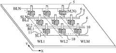
图1为本发明实施例提供的一种基于隧道磁阻效应的触觉传感器的结构示意图;1 is a schematic structural diagram of a tactile sensor based on the tunnel magnetoresistance effect provided by an embodiment of the present invention;
图2为本发明实施例提供的一种磁隧道结单元的磁矩图;2 is a magnetic moment diagram of a magnetic tunnel junction unit provided by an embodiment of the present invention;
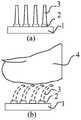
图3为本发明实施例提供的一种触觉传感器对外部物体感应的示意图;3 is a schematic diagram of a tactile sensor sensing an external object according to an embodiment of the present invention;
图4为本发明实施例提供的一种自由层磁矩方向的示意图;4 is a schematic diagram of a magnetic moment direction of a free layer according to an embodiment of the present invention;
图5为本发明实施例提供的另一种自由层磁矩方向的示意图;5 is a schematic diagram of another free layer magnetic moment direction provided by an embodiment of the present invention;
图6为本发明实施例提供的一种磁隧道结单元的R-H转换曲线图;6 is an R-H conversion curve diagram of a magnetic tunnel junction unit provided by an embodiment of the present invention;
图7为本发明实施例提供的另一种基于隧道磁阻效应的触觉传感器的结构示意图;7 is a schematic structural diagram of another tactile sensor based on the tunnel magnetoresistance effect provided by an embodiment of the present invention;
图8为本发明实施例提供的又一种基于隧道磁阻效应的触觉传感器的结构示意图;FIG. 8 is a schematic structural diagram of another tactile sensor based on the tunnel magnetoresistance effect provided by an embodiment of the present invention;
图9为本发明实施例提供的再一种基于隧道磁阻效应的触觉传感器的结构示意图;9 is a schematic structural diagram of still another tactile sensor based on the tunnel magnetoresistance effect provided by an embodiment of the present invention;
图10为本发明实施例提供的磁隧道结单元的通断方式示意图;10 is a schematic diagram of an on-off manner of a magnetic tunnel junction unit provided by an embodiment of the present invention;
图11为本发明实施例提供的又一种基于隧道磁阻效应的触觉传感器的结构示意图;11 is a schematic structural diagram of another tactile sensor based on the tunnel magnetoresistance effect provided by an embodiment of the present invention;
图12为本发明实施例提供的另一种磁隧道结单元的通断方式示意图;12 is a schematic diagram of an on-off manner of another magnetic tunnel junction unit provided by an embodiment of the present invention;
图13为本发明实施例提供的再一种基于隧道磁阻效应的触觉传感器的结构示意图;13 is a schematic structural diagram of still another tactile sensor based on the tunnel magnetoresistance effect provided by an embodiment of the present invention;
图14为本发明实施例提供的又一种磁隧道结单元的通断方式示意图;14 is a schematic diagram of another on-off mode of a magnetic tunnel junction unit provided by an embodiment of the present invention;
图15为本发明实施例提供的一种触柱材料的制备方法的示意图;15 is a schematic diagram of a method for preparing a contact post material provided by an embodiment of the present invention;
图16为本发明实施例提供的一种触柱在磁隧道结单元上的制备方法的示意图;16 is a schematic diagram of a method for preparing a contact post on a magnetic tunnel junction unit according to an embodiment of the present invention;
图17为本发明实施例提供的四种磁隧道结单元的俯视形状示意图;17 is a schematic top-view shape diagram of four types of magnetic tunnel junction units provided in an embodiment of the present invention;
图18为本发明实施例提供的一种触觉传感器的数据处理方式示意图;18 is a schematic diagram of a data processing method of a tactile sensor provided by an embodiment of the present invention;
图19为本发明实施例提供的另一种触觉传感器的数据处理方式示意图。FIG. 19 is a schematic diagram of another data processing manner of a tactile sensor provided by an embodiment of the present invention.
具体实施方式Detailed ways
下面结合附图和实施例对本发明作进一步的详细说明。可以理解的是,此处所描述的具体实施例仅仅用于解释本发明,而非对本发明的限定。另外还需要说明的是,为了便于描述,附图中仅示出了与本发明相关的部分而非全部结构。The present invention will be further described in detail below in conjunction with the accompanying drawings and embodiments. It should be understood that the specific embodiments described herein are only used to explain the present invention, but not to limit the present invention. In addition, it should be noted that, for the convenience of description, the drawings only show some but not all structures related to the present invention.
图1为本发明实施例提供的一种基于隧道磁阻效应的触觉传感器的结构示意图,如图1所示,该触觉传感器包括:柔性衬底1;在柔性衬底1上分别沿第一方向X和第二方向Y呈阵列分布的M*N个磁隧道结单元2;沿着柔性衬底1指向磁隧道结单元2的方向,各磁隧道结单元2均包括依次层叠设置的下电极层21、钉扎层22、绝缘层23、自由层24和上电极层25;其中,自由层24的磁致伸缩系数λs不为零,自由层24的磁矩方向与钉扎层22的磁矩方向的夹角在45°~135°或-135°~-45°之间;FIG. 1 is a schematic structural diagram of a tactile sensor based on the tunnel magnetoresistance effect provided by an embodiment of the present invention. As shown in FIG. 1 , the tactile sensor includes: a
与各磁隧道结单元2一一对应设置的触柱3,触柱3设置在磁隧道结单元2远离柔性衬底1的一侧表面;当外界物体接触触柱3时,触柱3发生形变并向磁隧道结单元2施加应力,导致自由层24的磁矩方向发生变化;The
至少一条第一信号线5,设置于柔性衬底1上并分别与各磁隧道结单元2的上电极层25电连接;At least one
至少一条第二信号线6,设置于柔性衬底1上并分别与各磁隧道结单元2的下电极层21电连接;第一信号线5和第二信号线6用于对磁隧道结单元2的输出电压值进行检测;At least one
其中,M和N为大于0的整数,第一方向X和第二方向Y均与柔性衬底1平行,且第一方向X与第二方向Y相交。Wherein, M and N are integers greater than 0, both the first direction X and the second direction Y are parallel to the
具体地,如图1中所示,该触觉传感器包括:柔性衬底1;柔性衬底1可以为减薄的硅,或者聚合物材料,例如聚二甲基硅氧烷(Polydimethylsiloxane,PDMS)、聚甲基丙烯酸甲酯(polymethyl methacrylate,PMMA)、聚酰亚胺(Polyimide,PI)、聚酰亚胺薄膜(Kapton)和聚氯乙烯(Polyvinyl chloride,PVC)等材料,但不限于此。设置柔性衬底1能够提升整体触觉传感器的柔性,使触觉传感器满足多领域应用需求。Specifically, as shown in FIG. 1 , the tactile sensor includes: a
继续参考图1,本发明中,触觉传感器还包括在柔性衬底1上分别沿第一方向X和第二方向Y呈阵列分布的M*N个磁隧道结单元2,也即,M*N个磁隧道结单元2在第一方向X和第二方向Y上阵列分布构成磁隧道结阵列。其中,M和N为大于0的整数,第一方向X和第二方向Y均与柔性衬底1平行,且第一方向X与第二方向Y相交。图1中示例性的示出了第一方向X为柔性衬底1的行方向,第二方向Y为柔性衬底1的列方向,实际设置情况不限于此。以第一方向X为行方向,磁隧道结阵列中包括N行、M列磁隧道结单元2。对于磁隧道结单元2的制作方式,本发明实施例不做限制,本领域技术人员可根据实际情况进行设置,例如可使用标准大规模集成制造技术制造,但不限于此。可以以坐标(x,y)形式表示各位置处的磁隧道结单元2,如(1,1)代表第一列第一行的磁隧道结单元2,(M,N)即代表第M列第N行的磁隧道结单元2。Continuing to refer to FIG. 1 , in the present invention, the tactile sensor further includes M*N magnetic
每个磁隧道结单元2均包括下电极层21、钉扎层22、绝缘层23、自由层24和上电极层25,沿着柔性衬底1指向磁隧道结单元2的方向,下电极层21、钉扎层22、绝缘层23、自由层24和上电极层25依次层叠排列,下电极层21靠近柔性衬底1。其中,自由层24的磁致伸缩系数λs不为零,自由层24的磁矩方向与钉扎层22的磁矩方向的夹角在45°~135°或-135°~-45°之间。Each magnetic
磁隧道结单元2的工作原理可简单描述如下:隧道磁阻效应来源于钉扎层22和自由层24的磁矩方向的相对取向,当钉扎层22和自由层24的磁矩方向相同时,电流流过磁隧道结单元2时遇到阻力较小,对应于低电阻状态。当钉扎层22和自由层24的磁矩方向相反时,电流流过磁隧道结单元2时阻力较大,对应于高电阻状态。为使钉扎层22和自由层24的磁矩方向相反而获得较大的隧道磁阻效应,一般采用反铁磁材料的交换偏置效应对钉扎层22的磁矩方向进行钉扎,使其不能自由转向;而自由层24可随外加磁场发生自由转向。当正向或反向的外加磁场超过自由层24的矫顽场时,可以实现磁矩方向的平行或反平行两种状态,产生磁隧道结单元2电阻的极小和极大值。The working principle of the magnetic
本发明中,设置自由层24的磁致伸缩系数λs不为零,并且自由层24与钉扎层22的磁矩方向之间的夹角在45°~135°或-135°~-45°范围内,也即,相对于磁矩方向固定的钉扎层22,自由层24的磁矩方向可在45°~135°或-135°~-45°范围内变化。由此使得磁隧道结单元2的隧道磁阻效应比较强,磁隧道结单元2的电阻对外加磁场的磁场强度的感应更加灵敏,提高了触觉传感器的灵敏度。图2为本发明实施例提供的一种磁隧道结单元的磁矩图,图中以FL表示自由层24的磁矩方向,PL表示钉扎层22的磁矩方向。如图2所示,自由层24与钉扎层22的磁矩方向之间的夹角在45°~135°或-135°~-45°范围内。In the present invention, the magnetostrictive coefficient λs of the
可仍参考图1,触觉传感器还包括:与各磁隧道结单元2一一对应设置的触柱3,也即,在柔性衬底1上分别沿第一方向X和第二方向Y呈阵列分布的M*N个触柱3。触柱3设置在磁隧道结单元2远离柔性衬底1的一侧表面,并与磁隧道结单元2直接接触。图3为本发明实施例提供的一种触觉传感器对外部物体感应的示意图,图3中(a)图为触觉传感器未接触外部物体时触柱3的状态,图3中(b)图为触觉传感器与外部物体接触时触柱3的状态,图3中示例性的示出了手指为外部物体,实际情况不限于此。可参考图1和图3,触柱3具有柔性,当外界物体接触触柱3时,触柱3会发生形变并向磁隧道结单元2施加应力,此应力即可以为拉应力也可以为压应力,当磁隧道结单元2受到外部应力时,外部应力的各向异性场引起导致自由层24的磁矩方向的变化,进而导致磁隧道结单元2的电阻发生变化。当磁隧道结单元2中通入电流时,即可根据检测到的各磁隧道结单元2处的输出电压值来确定应力的分布,进而实现对外部物体的感知。Still referring to FIG. 1 , the tactile sensor further includes: the contact posts 3 arranged in a one-to-one correspondence with each magnetic
进一步地,本发明中,触觉传感器还包括至少一条第一信号线5和至少一条第二信号线6,第一信号线5和第二信号线6均在设置在柔性衬底1上,第一信号线5与各磁隧道结单元2的上电极层25电连接,第二信号线6与各磁隧道结单元2的下电极层21电连接。Further, in the present invention, the tactile sensor further includes at least one
可以理解的是,当各磁隧道结单元2的电阻发生变化时,其两端的输出电压也会发生变化,因此,可设置第一信号线5和第二信号线6,通过第一信号线5和第二信号线6即可检测到磁隧道结单元2处的输出电压值,由此得到整个触觉传感器的应力分布情况。It can be understood that when the resistance of each magnetic
其中,对于第一信号线5和第二信号线6的具体布线方式,本发明实施例不做限制,本领域技术人员可根据实际需求进行设置,只需保证通过第一信号线5和第二信号线6能够准确检测到磁隧道结阵列中不同位置处的各磁隧道结单元2的输出电压值。The specific wiring methods of the
应力的各向异性场的大小与应力的关系可根据以下公式计算:The relationship between the magnitude of the anisotropic field of stress and the stress can be calculated according to the following formula:

其中,HKS为应力的各向异性场,λs为自由层的磁致伸缩系数,σ为所受应力的大小,MS为自由层的饱和磁矩。Among them,HKS is the anisotropic field of stress,λs is the magnetostrictive coefficient of the free layer, σ is the magnitude of the stress, and MS is the saturation magnetic moment of the free layer.
进一步地,以HKM表示施加应力前自由层24的各向异性场,HK表示施加应力后自由层24的各向异性场即自由层24实际的各向异性场,以HKS表示应力的各向异性场,三者的关系满足以下公式:Further, HKM represents the anisotropy field of the

施加应力后自由层24各向异性场为应力的各向异性场和施加应力前自由层24的各向异性场的矢量和。图4为本发明实施例提供的一种自由层磁矩方向的示意图,图5为本发明实施例提供的另一种自由层磁矩方向的示意图。图4中示出了磁隧道结单元2受到的为拉应力,应力σ大于零,且自由层24的磁致伸缩系数λs大于零的情况,图4和图5中以HKS代表应力的各向异性场的磁矩方向,HKM代表施加应力前自由层24的各向异性场的磁矩方向,FL代表施加应力后自由层24的各向异性场的磁矩方向,也即自由层24的实际的各向异性场的磁矩方向。如图4所示,当磁致伸缩系数λs大于零时,应力σ的各向异性场的磁矩方向与应力的方向一致,使得自由层24的磁矩向应力σ作用的方向偏转


可以理解的是,当磁隧道结单元2受到的为压应力的时候,应力σ小于零。此时若自由层24的磁致伸缩系数λs大于零,则应力的各向异性场的磁矩方向与应力的方向垂直,使得自由层24的磁矩向远离应力作用的方向偏转;若自由层24的磁致伸缩系数λs小于零,则应力的各向异性场的磁矩方向与应力的方向一致,使得自由层24的磁矩向应力作用的方向偏转。It can be understood that when the magnetic
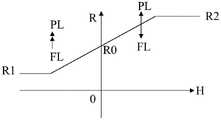
图6为本发明实施例提供的一种磁隧道结单元的R-H转换曲线图,图6中仍以FL表示自由层24的磁矩方向,以PL表示钉扎层22的磁矩方向。参考图6,在应力等于零的情况下,沿钉扎层22的磁矩方向,应力的各向异性场磁场强度H等于零,此时磁隧道结单元2的电阻为R0。当应力的各向异性场的磁矩方向与钉扎层22的磁矩方向一致时,随着应力的各向异性场强度H的逐渐增加,自由层24的磁矩方向与钉扎层22的磁矩方向逐渐趋向一致,此时磁隧道结单元2的电阻逐渐变小;当自由层24的磁矩方向与钉扎层22的磁矩方向完全相同时,磁隧道结单元2的电阻达到最小值R1。当应力的各向异性场的磁矩方向与钉扎层22的磁矩方向相反时,随着应力的各向异性场强度H的增加,自由层24的磁矩方向与钉扎层22的磁矩方向逐渐相反,此时磁隧道结单元2的电阻逐渐增大;当自由层24的磁矩方向与钉扎层22的磁矩方向完全相反时,磁隧道结单元2的电阻达到最大值R2。当应力的各向异性场的方向和强度发生变化时,磁隧道结单元2的电阻也会相应的发生变化,因此,可通过检测磁隧道结单元2的输出电压值来确定应力的分布情况。6 is an R-H conversion curve diagram of a magnetic tunnel junction unit provided by an embodiment of the present invention. In FIG. 6 , the magnetic moment direction of the
另外,本发明中,设置自由层24和钉扎层22的磁矩方向夹角在45°~135°或-135°~-45°内,也能够使磁隧道结单元2的电阻随着应力的各向异性场发生如图6中所示的线性变化,提高磁隧道结单元2检测的准确性。In addition, in the present invention, the included angle of the magnetic moment direction of the
进一步地,磁隧道结单元2的电阻R和自由层24的实际各向异性场HK的关系可表示为:Further, the relationship between the resistance R of the magnetic
dR/dH=C/Hk (3)dR/dH=C/Hk (3)
在施加应力前自由层24的各向异性场HKM不变的情况下,自由层24的实际各向异性场HK正比于应力σ和自由层24磁致伸缩系数λs的乘积,即HK正比于应σλs。磁隧道结单元2的电阻R与应力σ存在如下关系:Under the condition that the anisotropy field HKM of the
dR/dσ=C1/λs (4)dR/dσ=C1/λs (4)
其中C和C1为常数。where C and C1 are constants.
当计算出各磁隧道结单元处的输出电压值后,能够转换为磁隧道结单元的电阻,进而根据上述公式,得到应力的方向及大小等,获得磁隧道结单元的应力分布情况。After calculating the output voltage value of each magnetic tunnel junction unit, it can be converted into the resistance of the magnetic tunnel junction unit, and then according to the above formula, the direction and magnitude of the stress can be obtained, and the stress distribution of the magnetic tunnel junction unit can be obtained.
本发明实施例中,在柔性衬底上形成由M*N个磁隧道结单元构成的磁隧道结阵列,基于磁隧道结单元的隧道磁阻效应实现对外部物体的感知。单个磁隧道结单元的尺寸为微米、亚微米数量级,既可以形成高分辨率的触觉传感器,也能实现触觉传感器的小型化应用;另外,设置自由层的磁致伸缩系数不为零,并且自由层与钉扎层的磁矩方向之间的夹角在45°~135°或-135°~-45°范围内,使得磁隧道结单元的隧道磁阻效应比较强,磁隧道结单元的电阻对外加磁场的磁场强度的感应更加灵敏,提高了触觉传感器的灵敏度。In the embodiment of the present invention, a magnetic tunnel junction array composed of M*N magnetic tunnel junction units is formed on the flexible substrate, and the perception of external objects is realized based on the tunnel magnetoresistance effect of the magnetic tunnel junction units. The size of a single magnetic tunnel junction unit is in the order of micrometers and submicrometers, which can not only form high-resolution tactile sensors, but also realize the miniaturization of tactile sensors; in addition, the magnetostriction coefficient of the free layer is not zero, and the free The angle between the magnetic moment direction of the layer and the pinned layer is in the range of 45°~135° or -135°~-45°, so that the tunnel magnetoresistance effect of the magnetic tunnel junction unit is relatively strong, and the resistance of the magnetic tunnel junction unit is relatively strong. The induction of the magnetic field strength of the external magnetic field is more sensitive, and the sensitivity of the tactile sensor is improved.
可选的,在一可能的实施例中,触觉传感器还可包括软磁屏蔽层;软磁屏蔽层设置于柔性衬底和磁隧道结单元之间;或者,软磁屏蔽层设置在磁隧道结单元与触柱之间。Optionally, in a possible embodiment, the tactile sensor may further include a soft magnetic shielding layer; the soft magnetic shielding layer is arranged between the flexible substrate and the magnetic tunnel junction unit; or, the soft magnetic shielding layer is arranged on the magnetic tunnel junction between the unit and the post.
图7为本发明实施例提供的另一种基于隧道磁阻效应的触觉传感器的结构示意图,如图7所示,本实施例中,触觉传感器内还可设置软磁屏蔽层6,软磁屏蔽层6用于解决外磁场存在条件下的触觉传感器的磁屏蔽问题。对于软磁屏蔽层6的设置位置,本发明实施例不做限制。FIG. 7 is a schematic structural diagram of another tactile sensor based on the tunnel magnetoresistance effect provided by an embodiment of the present invention. As shown in FIG. 7 , in this embodiment, a soft
示例性的,在一种可能的实施方式中,如图7中,软磁屏蔽层6可设置在柔性衬底1与磁隧道结单元2之间,即可在柔性衬底1上先设置一层软磁屏蔽层6,然后在软磁屏蔽层6的上方制备磁隧道结单元2。Exemplarily, in a possible implementation manner, as shown in FIG. 7 , the soft
示例性的,在另一可能的实施方式中,软磁屏蔽层6可设置在磁隧道结单元2与触柱3之间,也即,设置在磁隧道结单元2的上电极层25表面。软磁屏蔽层6的存在能够对外界环境磁场起到较好的屏蔽作用,防止外界环境磁场对触觉传感器的工作造成影响。Exemplarily, in another possible implementation, the soft
可选的,在一可能的实施例中,软磁屏蔽层6为包含铁、钴和镍中的一种或多种元素的软磁合金材料。上述软磁合金材料的成本不高,利用上述软磁合金材料形成软磁屏蔽层6,既能保证对外界环境磁场的屏蔽效果,也能降低触觉传感器的制作成本。Optionally, in a possible embodiment, the soft
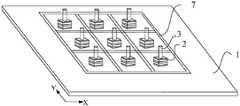
可选的,图8为本发明实施例提供的又一种基于隧道磁阻效应的触觉传感器的结构示意图,如图8所示,在一可能的实施例中,触觉传感器还可包括硬质材料层7;硬质材料层7设置于各磁隧道结单元2之间。Optionally, FIG. 8 is a schematic structural diagram of another tactile sensor based on the tunnel magnetoresistance effect provided by an embodiment of the present invention. As shown in FIG. 8 , in a possible embodiment, the tactile sensor may further include a
具体地,参考图8,本实施例中,还可在柔性衬底1上设置硬质材料层7,硬质材料层7设置在各磁隧道结单元2之间,也即硬质材料层7围绕在各磁隧道结单元2之间,形成网格状结构,以将各磁隧道结单元2分开。这样设置的好处在于,当某磁隧道结单元2上方的触柱3受到应力形变时,触柱3的弯曲形变能够有效传递至该磁隧道结单元2,并且不会影响其他磁隧道结单元2的磁场,进而保证触觉传感器的灵敏度与准确度。Specifically, referring to FIG. 8 , in this embodiment, a
其中,可选的,硬质材料层7可以利用Si3N4、Al2O3、SiO2等绝缘材料形成,但不限于此,本领域技术人员可根据实际需求进行选择。Wherein, optionally, the
可仍参考图7,当触觉传感器同时包括软磁屏蔽层6和硬质材料层7时,可先在柔性衬底1上设置软磁屏蔽层6,设置软磁屏蔽层6时,在各磁隧道结单元2的四周留有狭槽窗口61,然后在狭槽窗口61内设置硬质材料层7,保证各磁隧道结单元2的柔性变形不受软磁屏蔽层6的影响。Still referring to FIG. 7 , when the tactile sensor includes the soft
可选的,可继续参考图1,在一可能的实施例中,第一信号线5和第二信号线6可参照如下方式进行设置。其中,第一信号线5包括N条,第二信号线6包括M条;N条第一信号线5沿第一方向X延伸并在第二方向Y上排列;在第一方向X上排列的M个磁隧道结单元2与对应排布的同一条第一信号线5电连接;M条第二信号线6沿第二方向Y延伸并在第一方向X上排列;在第二方向Y上排列的N个磁隧道结单元2与对应排布的同一条第二信号线6电连接。Optionally, referring to FIG. 1 , in a possible embodiment, the
具体地,柔性衬底1上可设置沿第一方向X延伸并在第二方向Y排列的N条第一信号线5以及沿第二方向Y延伸并在第一方向X排列的M条第二信号线6,即图1中所示行方向的N条第一信号线5和列方向的M条第二信号线6。在第一方向X排列的M个磁隧道结单元2与对应排布的同一条第一信号线5电连接,也即,每行中的M个磁隧道结单元2均与同一条第一信号线5电连接,例如第N行的M个磁隧道结单元2与第N条第一信号线5电连接。同样的,沿第二方向Y排列的N个磁隧道结单元2与对应排布的同一条第二信号线6电连接,也即,每列中的N个磁隧道结单元2与同一条第二信号线6电连接,例如,第M列的N个磁隧道结单元2与第M条第二信号线6电连接。位置(M,N)处的磁隧道结单元2分别与第N条第一信号线5和第M条第二信号线6连接。图中以C(1)~C(M)表示第一方向X排列的M条第一信号线5,R(1)~(N)表示第二方向Y排列的N条第一信号线5。Specifically, N
其中,图1中示例性的示出了同一行方向的各磁隧道结单元2的上电极层25分别与一条第一信号线5电连接,同一列方向的各磁隧道结单元2的下电极层21分别与一条第二信号线6电连接;在其他实施例中,也设置同一行方向的各磁隧道结单元2的下电极层21分别与一条第二信号线6电连接,同一列方向的各磁隧道结单元2的上电极层25分别与一条第一信号线5电连接,只需保证通过第一信号线5和第二信号线6能够采集到磁隧道结单元2整体的输出电压值。1 exemplarily shows that the upper electrode layer 25 of each magnetic
这样设置的好处在于,在第一信号线5和第二信号线6与磁隧道结单元2均呈阵列排布,在通过第一信号线5和第二信号线6检测磁隧道结单元2的输出电压值时,能够较为准确的确定各磁隧道结单元2的位置,进而准确判断受到应力的区域。The advantage of this arrangement is that the
可选的,图9为本发明实施例提供的再一种基于隧道磁阻效应的触觉传感器的结构示意图,如图9中所示,在一可能的实施例中,触觉传感器还包括与各磁隧道结单元2一一对应设置的单向导通元件4;在第一方向X上排列的M个磁隧道结单元2的上电极层25分别通过一个单向导通元件4与同一条第一信号线5电连接;或者,在第二方向Y上排列的N个磁隧道结单元2的下电极层21分别通过一个单向导通元件4与同一条第二信号线6电连接。Optionally, FIG. 9 is a schematic structural diagram of another tactile sensor based on the tunnel magnetoresistance effect provided by an embodiment of the present invention. As shown in FIG. 9 , in a possible embodiment, the tactile sensor further includes The
具体地,本发明中,还可在触觉传感器中设置与各磁隧道结单元2一一对应连接的单向导通元件4。单向导通元件4可用来控制流向各磁隧道结单元2的电流,实现磁隧道结单元2的通断,也即,只有单向导通元件4正向导通时,磁隧道结单元2内才会有电流通过,磁隧道结单元2的电压值能够被检测到。Specifically, in the present invention, the tactile sensor may also be provided with a one-way
图9中示例性的是示出了第一方向X上排列的M个磁隧道结单元2的上电极层25分别通过一个单向导通元件4与同一条第一信号线5电连接,单向导通元件4的正极连接第一信号线5,负极连接磁隧道结单元2的上电极层25,此时,在第二方向Y排列的N个磁隧道结单元2的下电极层21可直接与一条第二信号线6电连接。FIG. 9 exemplarily shows that the upper electrode layers 25 of the M magnetic
或者,在其他实施例中,也可设置在第二方向Y上排列的N个磁隧道结单元2的下电极层21分别通过一个单向导通元件4用同一条第二信号线6电连接,单向导通元件4的正极连接磁隧道结单元2的下电极层21,负极连接第二信号线6,此时,在第一方向X排列的M个磁隧道结单元2的上电极层25可直接与一条第一信号线5电连接。Alternatively, in other embodiments, the lower electrode layers 21 of the N magnetic
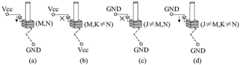
本实施例中以单向导通元件4为二极管为例,对单向导通元件4的工作过程进行介绍。图10为本发明实施例提供的磁隧道结单元的通断方式示意图,图10中示出了图9所示二极管连接方式下磁隧道结单元2的通断方式,如图10中(a)图所示,与位置(M,N)处的磁隧道结单元2相连的二极管的正极接收电源信号Vcc,同时该磁隧道结单元2的下电极层21接收接地信号GND,位置(M,N)处的二极管导通,电流经上电极层25、自由层24、绝缘层23、钉扎层22传输至下电极层21,进而可通过第一信号线5和第二信号线6对该磁隧道结单元2的输出电压值进行检测。In this embodiment, the working process of the one-
参考图10中(b)图,与位置(M,K≠N)处的磁隧道结单元2相连的二极管的正极接收电源信号Vcc,同时向该磁隧道结单元2的下电极层21传输电源信号Vcc,位置(M,K≠N)处的二极管不导通,位置(M,K≠N)处的磁隧道结单元2处的输出电压值无法被检测。Referring to (b) in FIG. 10 , the anode of the diode connected to the magnetic
参考图10中(c)图,与位置(J≠M,N)处的磁隧道结单元2相连的二极管的正极接收接地信号GND,同时向该磁隧道结单元2的下电极层21传输接地信号GND,位置(J≠M,N)处的二极管不导通,位置(J≠M,N)处的磁隧道结单元2处的输出电压值无法被检测。Referring to (c) in FIG. 10 , the anode of the diode connected to the magnetic
参考图10中(d)图,与位置(J≠M,K≠N)处的磁隧道结单元2相连的二极管的正极接收接地信号GND或者电源信号Vcc,同时向该磁隧道结单元2的下电极层21传输接地信号GND或者电源信号Vcc,位置(J≠M,K≠N)处的二极管不导通,位置(J≠M,K≠N)处的磁隧道结单元2处的输出电压值无法被检测。图中所述黑色箭头代表电流可通过,“×”表示电流无法通过。Referring to (d) in FIG. 10 , the anode of the diode connected to the magnetic
可以理解的是,电源信号Vcc或接地信号GND是以很快的频率在各磁隧道结单元2扫描传输,当位置(M,N)处的磁隧道结单元2受到触柱3对其施加的应力,同时(M,N)处对应的二极管导通,即可通过第一信号线5和第二信号线6检测该磁隧道结单元2的电压。It can be understood that the power signal Vcc or the ground signal GND scans and transmits in each magnetic
可选的,控制二极管导通或关断的信号,如电源信号Vcc和接地信号GND可由其他图中未示出的信号线或电路发出,本发明实施例不限定具体方式。Optionally, the signals for controlling the diode to be turned on or off, such as the power signal Vcc and the ground signal GND, can be sent by signal lines or circuits not shown in other figures, and the embodiment of the present invention does not limit the specific manner.
可选的,上述实施例中通过设置单向导通元件4来控制对磁隧道结单元2输出电压的检测,在其他实施例中,也可设置开关元件对流向磁隧道结单元2的电流进行控制。Optionally, in the above embodiment, the detection of the output voltage of the magnetic
图11为本发明实施例提供的又一种基于隧道磁阻效应的触觉传感器的结构示意图,图12为本发明实施例提供的另一种磁隧道结单元的通断方式示意图。参考图11和图12,本实施例中,触觉传感器可包括与第一信号线5一一对应电连接的第一开关元件8、与第二信号线6一一对应电连接的第二开关元件9。当第一开关元件8和第二开关元件9同时导通时,对应的磁隧道结单元2的电压值可以被检测到。本实施例中,示例性的设置第一开关元件8和第二开关元件9均为MOS管,实际设置方式不限于此。11 is a schematic structural diagram of another tactile sensor based on the tunnel magnetoresistance effect provided by an embodiment of the present invention, and FIG. 12 is a schematic diagram of another on-off manner of a magnetic tunnel junction unit provided by an embodiment of the present invention. Referring to FIGS. 11 and 12 , in this embodiment, the tactile sensor may include a
具体地,参考图11,仍以第一方向X为行方向,第二方向Y为列方向为例,触觉传感器还可包括N个沿第二方向Y即列方向排列的第一开关元件8,每个第一开关元件8分别与相应的第一信号线5连接,也即,在第二方向Y上,第N个第一开关元件8与第N条第一信号线5连接。同样的,触觉传感器还包括M个沿第一方向X即行方向排列的第二开关元件9,每个第二开关元件9分别与相应的第二信号线6连接,也即,在第一方向X上,第M个第二开关元件9与第M条第二信号线6连接。Specifically, referring to FIG. 11 , still taking the first direction X as the row direction and the second direction Y as the column direction as an example, the tactile sensor may further include N first switching
参考图12中的(a)图,与第N行第一信号线5相连的MOS管31接收电源信号Vcc,与第M列第二信号线6相连的MOS管32接收接地信号GND,同时MOS管31的控制端和MOS管32的控制端接收导通控制信号,MOS管31和MOS管32同时导通,则位置(M,N)处的磁隧道结单元2的输出电压值能够被检测。Referring to (a) of FIG. 12 , the
参考图12中的(b)图,与第N行第一信号线5相连的MOS管31接收电源信号Vcc,与第J(J≠M)列第二信号线6相连的MOS管33接收接地信号GND,同时MOS管31的控制端接收导通控制信号,MOS管33的控制端接收关断控制信号,MOS管31导通,MOS管33关断,位置(J≠M,N)处的磁隧道结单元2的输出电压值不能被检测。Referring to (b) in FIG. 12 , the
参考图12中的(c)图,与第K(K≠N)行第一信号线5相连的MOS管34接收电源信号Vcc,与第M列第二信号线6相连的MOS管32接收接地信号GND,同时MOS管34的控制端接收关断控制信号,MOS管34关断,位置(M,K≠N)处的磁隧道结单元2的输出电压值不能被检测。Referring to (c) in FIG. 12 , the
参考图12中的(d)图,与第K(K≠N)行第一信号线5相连的MOS管34接收电源信号Vcc,与第J(J≠M)列第二信号线6相连的MOS管33接收接地信号GND,此时的MOS管34和MOS管33都不导通,则位置(J≠M,K≠N)处的磁隧道结单元2的输出电压值不能被检测。Referring to Fig. 12 (d), the
可选的,图13为本发明实施例提供的再一种基于隧道磁阻效应的触觉传感器的结构示意图。本实施例中,第一信号线5和第二信号线6均包括N条;N条第一信号线5与N条第二信号线6均沿第一方向X延伸并在第二方向Y上排列;在第一方向X上排列的M个磁隧道结单元2的上电极层25分别与对应排布的同一条第一信号线5电连接,在第一方向X上排列的M个磁隧道结单元2的下电极层21分别与对应排布的同一条第二信号线6电连接。Optionally, FIG. 13 is a schematic structural diagram of still another tactile sensor based on the tunnel magnetoresistance effect provided by an embodiment of the present invention. In this embodiment, both the
本实施例中,可设置第一信号线5和第二信号线6在同一方向上延伸并在同一方向上排列,图13中示例性的示出了第一信号线5和第二信号线6均在第一方向X延伸、在第二方向Y排列,实际设置情况不限于此。这样设置的好处在于,可以简化第一信号线5和第二信号线6的制备工艺,减少触觉传感器的制作周期。图13中以BL1代表第1条第一信号线、BLN代表第N条第一信号线6、SL1代表第1条第二信号线6、SLN代表第N条第二信号线6。In this embodiment, the
可选的,第一信号线5和第二信号线6的此种设置方式下,可采用以下方式对各磁隧道结单元2的通断方式进行设置。触觉传感器还可包括与各磁隧道结单元2一一对应设置的第三开关元件10;在第一方向X上排列的M个磁隧道结单元2的上电极层25分别通过一个第三开关元件10与同一条第一信号线5电连接;或者,在第一方向X上排列的M个磁隧道结单元2的下电极层21分别通过一个第三开关元件10与同一条第二信号线6电连接。Optionally, in this arrangement of the
对于第三开关元件10的类型,本发明实施例不做限制,本领域技术人员可根据实际需求进行设置,本实施例中,第三开关元件10仍可以为MOS管。The type of the
具体地,可设置在第一方向X上排列的M个磁隧道结单元2的上电极层25分别通过一个MOS管与同一条第一信号线5电连接,在第一方向X上排列的M个磁隧道结单元2的下电极层21可直接与同一条第二信号线6电连接;或者,在第一方向X上排列的M个磁隧道结单元2的下电极层21分别通过一个MOS管与同一条第二信号线6电连接,此时在第一方向X上排列的M个磁隧道结单元2的上电极层25可直接与一条第一信号线5电连接。Specifically, the upper electrode layers 25 of the M magnetic
其中,柔性衬底1上还包括在第二方向Y延伸、第一方向X上排列M条控制信号线11,在第二方向Y上排列的各MOS管的控制端连接同一条控制信号线11,MOS管根据控制信号线11传输的信号导通或关断,当MOS管导通时,对应的磁隧道结单元2的输出电压值可以被检测到。图13中WL1代表第1条控制信号线11,WLM代表第M条控制信号线11。图13中所示为上述第二种可选的设置方式,根据图13,本领域技术人员能够得出第一种设置方式下MOS管的具体设置方式,此处不再进行详细说明。The
图14为本发明实施例提供的又一种磁隧道结单元的通断方式示意图。图14中磁隧道结单元2的通断方式与图13中信号线的设置方式对应。如图14中(a)图,第N行第一信号线5和第N行第二信号线6分别连接电源信号Vcc和接地信号GND,第M列控制信号线为开通模式,即传输导通控制信号,此时位置(M,N)处的磁隧道结单元2处的输出电压值能够被检测。FIG. 14 is a schematic diagram of another on-off manner of a magnetic tunnel junction unit provided by an embodiment of the present invention. The on-off mode of the magnetic
参考图14(b),第N行第一信号线5和第N行第二信号线6分别连接电源信号Vcc和接地信号GND,第J列控制信号线为关闭模式,即第J(J≠M)列控制信号线传输关断控制信号,此时位置(J≠M,N)处的磁隧道结单元2处的输出电压值不能够被检测。Referring to FIG. 14(b), the
参考图14(c),第K行第一信号线5和第K行第二信号线6均连接接地信号GND或电源信号Vcc,此时第M列控制信号线虽然为开通模式,但是第K(K≠N)行第一信号线5和第K行第二信号线6为等电位的GND或者Vcc,此时位置(K≠N,M)处的磁隧道结单元2处的输出电压值不能够被检测。Referring to FIG. 14( c ), the
参考图14(d),若要使得位置(K≠N,J≠M)处的磁隧道结单元2处的输出电压值不能够被检测。可通过控制第K行第一信号线5和第K行第二信号线6均连接接地信号GND或电源信号Vcc,或者控制第J列控制信号线为关闭模式,又或者使得第K行第一信号线5和第K行第二信号线6反电位,即分别为接地信号GND和电源信号Vcc。Referring to FIG. 14( d ), the output voltage value at the magnetic
可选的,在一可能的实施例中,自由层24的材料为钴铁硼、钴铁或镍铁合金。Optionally, in a possible embodiment, the material of the
本实施例中,可选择磁致伸缩系数λs大于零的钴铁硼、钴铁或镍铁合金来制备自由层24,上述材料的磁致伸缩系数λs较大,利用上述材料形成自由层24,磁隧道结单元2隧道磁阻效应较为明显,能够提高触觉传感器的灵敏度。In this embodiment, cobalt-iron-boron, cobalt-iron or nickel-iron alloys with a magnetostrictive coefficient λs greater than zero can be selected to prepare the
可选的,在一可能的实施例中,触柱3为非磁性材料。本实施例中,可采用非磁性材料形成触柱3,避免触柱3对磁隧道结单元2处的磁场产生影响。触柱3不但要求具有一定强度,而且要求具有柔性,在和外部物体接触时能够产生变形,因此可选择聚合物和纳米材料来制备触柱3,例如聚合物可选PDMS,纳米材料可为纳米丝,纳米管、纳米颗粒等。Optionally, in a possible embodiment, the
可选的,对于各磁隧道结单元2上的触柱3的形成方式,本发明实施例不做限制,本领域技术人员可根据实际需求进行设置。Optionally, the manner of forming the contact posts 3 on each magnetic
示例性的,图15为本发明实施例提供的一种触柱材料的制备方法的示意图,如图15所示,首先提供铝衬底51,对铝衬底51进行第一次阳极氧化,在铝衬底51表面形成多孔的第一氧化铝结构52;再将表面的第一氧化铝结构52溶解掉,得到较为平整的铝表面510。紧接着,对铝衬底51进行第二次阳极氧化,形成均匀分布的孔径531直径约35nm的第二氧化铝结构53,然后对第二氧化铝结构53的底部54进行适当腐蚀,使得孔径531直接和铝衬底51接触;进一步地,采用电镀的方法在孔径531中电镀生长纳米丝55,如可以是纳米铁、纳米铜、纳米镍铁或者纳米镍丝等,然后对第二氧化铝结构53进行溶解释放,得到触柱材料55。Exemplarily, FIG. 15 is a schematic diagram of a method for preparing a contact post material according to an embodiment of the present invention. As shown in FIG. 15 , an
图16为本发明实施例提供的一种触柱在磁隧道结单元上的制备方法的示意图,如图16所示,将上述过程制备得到的触柱材料55分散在聚合物如PDMS56中,形成纳米材料混合物57,其中触柱材料55和PDMS56的体积比可为10-20%,以保持流动性。进一步地,在制备好的柔性衬底1的上的磁隧道结单元2的上方旋涂PDMS层58,并加热固化,然后将纳米混合物57转移到固化的PDMS层58表面,同时将表面有触柱孔591的PMMA模板59定位在固化的PDMS层58表面,这样纳米材料混合物57进入PMMA模板59的触柱孔591中,然后加热固化纳米材料混合物57形成触柱3,最后去除PMMA模板58,就可以得到触柱阵列。其中,PMMA模板58可以采用激光打孔的方法获得触柱孔591,也可以采用LIGA技术得到触柱孔591。FIG. 16 is a schematic diagram of a method for preparing a contact post on a magnetic tunnel junction unit provided by an embodiment of the present invention. As shown in FIG. 16 , the
可选的,图17为本发明实施例提供的四种磁隧道结单元的俯视形状示意图,本发明实施例中,磁隧道结单元2的俯视形状呈椭圆形、圆形、菱形、矩形或者方形。当触觉传感器的应用领域不同时,其结构也不尽相同,可根据实际应用需求设置磁隧道结单元2的具体形状,例如设置成椭圆形、圆形、菱形、矩形或者方形等,但不限于此。Optionally, FIG. 17 is a schematic diagram of top-view shapes of four types of magnetic tunnel junction units provided in an embodiment of the present invention. In this embodiment of the present invention, the top-view shape of the magnetic
可选的,在一可能的实施例中,触觉传感器还可包括偏置永磁体,用于提供偏置磁场,以确定磁隧道结单元在未受到应力时的初始电压值。具体地,偏置磁场的存在可以为自由层提高初始偏置磁矩,增加自由层的动态范围,提高磁场响应的线性度,并降低磁滞。外部磁场还可用来对准应力的各向异性场的磁矩,使得触柱向磁隧道结单元施加应力后,应力的各向异性场能够在自由层中诱发磁矩变化,从而自由层的磁矩方向与钉扎层的磁矩方向的夹角可在一定角度范围内变化。通过设置偏置磁场,还能对磁隧道结单元的R-H曲线的零点(即H=0)进行设置,进行确定磁隧道结单元在未受到应力时的初始电压值。Optionally, in a possible embodiment, the tactile sensor may further include a bias permanent magnet for providing a bias magnetic field to determine the initial voltage value of the magnetic tunnel junction unit when it is not under stress. Specifically, the existence of the bias magnetic field can increase the initial bias magnetic moment for the free layer, increase the dynamic range of the free layer, improve the linearity of the magnetic field response, and reduce the magnetic hysteresis. The external magnetic field can also be used to align the magnetic moment of the anisotropic field of stress, so that after the contact post applies stress to the magnetic tunnel junction unit, the anisotropic field of stress can induce a change in the magnetic moment in the free layer, so that the magnetic moment of the free layer is changed. The included angle between the direction of the moment and the direction of the magnetic moment of the pinning layer can be varied within a certain angle range. By setting the bias magnetic field, the zero point (ie, H=0) of the R-H curve of the magnetic tunnel junction unit can also be set to determine the initial voltage value of the magnetic tunnel junction unit when it is not under stress.
可选的,在一可能的实施例中,触觉传感器还可包括,信号处理电路(图中未示出);信号处理电路与第一信号线和第二信号线电连接,用于通过第一信号线和第二信号线检测各磁隧道结单元的输出电压值,并根据各磁隧道结单元的输出电压值确定各磁隧道结单元处的应力值,实现对外部物体的感知。Optionally, in a possible embodiment, the tactile sensor may further include a signal processing circuit (not shown in the figure); the signal processing circuit is electrically connected to the first signal line and the second signal line, and is used for passing the first signal line and the second signal line. The signal line and the second signal line detect the output voltage value of each magnetic tunnel junction unit, and determine the stress value at each magnetic tunnel junction unit according to the output voltage value of each magnetic tunnel junction unit, so as to realize the perception of external objects.
具体地,本发明实施例中,可设置信号处理电路,由信号处理电路进行各磁隧道结单元的输出电压值的采集,并根据各磁隧道结单元的输出电压值确定各磁隧道结单元处的应力值,实现对外部物体的感知。Specifically, in the embodiment of the present invention, a signal processing circuit may be provided, the signal processing circuit collects the output voltage value of each magnetic tunnel junction unit, and determines the position of each magnetic tunnel junction unit according to the output voltage value of each magnetic tunnel junction unit. The stress value can realize the perception of external objects.
其中,对于信号处理电路的设置位置,本发明实施例不做限制,本领域技术人员可根据实际需求设置。例如可设置在柔性电路板的边缘,或与柔性电路板分开设置等,此处不再详细说明。Wherein, the setting position of the signal processing circuit is not limited in the embodiment of the present invention, and those skilled in the art can set it according to actual requirements. For example, it may be arranged at the edge of the flexible circuit board, or be arranged separately from the flexible circuit board, etc., which will not be described in detail here.
当然,本申请中,也可不在触觉传感器中设置信号处理电路,单独设置处理器芯片等外部信号处理装置,由外部信号处理装置执行上述信号处理电路的功能,此时本申请中的触觉传感器可仅作为感应元件。Of course, in this application, a signal processing circuit may not be provided in the tactile sensor, and an external signal processing device such as a processor chip may be provided separately, and the external signal processing device performs the functions of the above-mentioned signal processing circuit. At this time, the tactile sensor in this application can be As an inductive element only.
图18为本发明实施例提供的一种触觉传感器的数据处理方式示意图,如图18所示,信号处理电路可将每个磁隧道结单元的输出电压值读出,并作出各磁隧道结单元的输出电压值分布图,进行根据输出电压值分布图确定应力分布,对外部物体进行感知。例如,位置(1,1)处的磁隧道结单元的输出电压值为V(1,1),位置(M,N)处的磁隧道结单元的输出电压值为V(M,N)。FIG. 18 is a schematic diagram of a data processing method of a tactile sensor provided by an embodiment of the present invention. As shown in FIG. 18 , the signal processing circuit can read out the output voltage value of each magnetic tunnel junction unit, and generate each magnetic tunnel junction unit. According to the output voltage value distribution diagram, the stress distribution is determined according to the output voltage value distribution diagram, and the external objects are sensed. For example, the output voltage value of the magnetic tunnel junction unit at the position (1, 1) is V(1, 1), and the output voltage value of the magnetic tunnel junction unit at the position (M, N) is V(M, N).
可选的,图19为本发明实施例提供的另一种触觉传感器的数据处理方式示意图,如图19所示,信号处理电路还可用于根据各磁隧道结单元的输出电压值计算相邻的磁隧道结单元的输出电压差值,进而确定相邻的磁隧道结单元的应力差值。Optionally, FIG. 19 is a schematic diagram of another data processing method of a tactile sensor provided by an embodiment of the present invention. As shown in FIG. 19 , the signal processing circuit can also be used to calculate adjacent magnetic tunnel junction units according to the output voltage value of each magnetic tunnel junction unit. The output voltage difference of the magnetic tunnel junction units is used to determine the stress difference of adjacent magnetic tunnel junction units.
具体地,可先读出各磁隧道结单元处的输出电压值,然后计算相邻的磁隧道结单元的输出电压差值,并作出磁隧道结阵列的输出电压差值分布图,进而确定磁隧道结阵列中各相邻的磁隧道结单元处的应力差值,实现对外部物体的感知。例如,位置(1,1)和(2,1)的磁隧道结单元的输出电压差值为V(2,1)-V(1,1),位置(M,N)和位置(M-1,N)处的磁隧道结单元的输出电压值为V(M,N)-(M-1,N)。图18和图19中仅示出了部分磁隧道结单元的输出电压值或输出电压差值,未示出全部磁隧道结单元的输出电压值或输出电压差值。Specifically, the output voltage value of each magnetic tunnel junction unit can be read first, and then the output voltage difference of adjacent magnetic tunnel junction units can be calculated, and the output voltage difference distribution map of the magnetic tunnel junction array can be drawn, and then the magnetic tunnel junction array can be determined. The stress difference at each adjacent magnetic tunnel junction unit in the tunnel junction array realizes the perception of external objects. For example, the output voltage difference of the magnetic tunnel junction cells at positions (1,1) and (2,1) is V(2,1)-V(1,1), position (M,N) and position (M- The output voltage value of the magnetic tunnel junction unit at 1,N) is V(M,N)-(M-1,N). FIG. 18 and FIG. 19 only show the output voltage values or output voltage difference values of some of the magnetic tunnel junction units, and do not show the output voltage values or output voltage difference values of all the magnetic tunnel junction units.
注意,上述仅为本发明的较佳实施例及所运用技术原理。本领域技术人员会理解,本发明不限于这里的特定实施例,对本领域技术人员来说能够进行各种明显的变化、重新调整、相互结合和替代而不会脱离本发明的保护范围。因此,虽然通过以上实施例对本发明进行了较为详细的说明,但是本发明不仅仅限于以上实施例,在不脱离本发明构思的情况下,还可以包括更多其他等效实施例,而本发明的范围由所附的权利要求范围决定。Note that the above are only preferred embodiments of the present invention and applied technical principles. Those skilled in the art will understand that the present invention is not limited to the specific embodiments herein, and various obvious changes, readjustments, combinations and substitutions can be made to those skilled in the art without departing from the protection scope of the present invention. Therefore, although the present invention has been described in detail through the above embodiments, the present invention is not limited to the above embodiments, and can also include more other equivalent embodiments without departing from the concept of the present invention. The scope is determined by the scope of the appended claims.
Claims (15)
Priority Applications (1)
| Application Number | Priority Date | Filing Date | Title |
|---|---|---|---|
| CN202210758444.6ACN115200751A (en) | 2022-06-29 | 2022-06-29 | Tactile sensor based on tunnel magnetoresistance effect |
Applications Claiming Priority (1)
| Application Number | Priority Date | Filing Date | Title |
|---|---|---|---|
| CN202210758444.6ACN115200751A (en) | 2022-06-29 | 2022-06-29 | Tactile sensor based on tunnel magnetoresistance effect |
Publications (1)
| Publication Number | Publication Date |
|---|---|
| CN115200751Atrue CN115200751A (en) | 2022-10-18 |
Family
ID=83578080
Family Applications (1)
| Application Number | Title | Priority Date | Filing Date |
|---|---|---|---|
| CN202210758444.6APendingCN115200751A (en) | 2022-06-29 | 2022-06-29 | Tactile sensor based on tunnel magnetoresistance effect |
Country Status (1)
| Country | Link |
|---|---|
| CN (1) | CN115200751A (en) |
Cited By (1)
| Publication number | Priority date | Publication date | Assignee | Title |
|---|---|---|---|---|
| CN119666035A (en)* | 2024-11-21 | 2025-03-21 | 武汉真友科技有限公司 | A tactile sensor and a method for manufacturing the same |
Citations (16)
| Publication number | Priority date | Publication date | Assignee | Title |
|---|---|---|---|---|
| US5650958A (en)* | 1996-03-18 | 1997-07-22 | International Business Machines Corporation | Magnetic tunnel junctions with controlled magnetic response |
| US20020073785A1 (en)* | 2000-12-20 | 2002-06-20 | Shiva Prakash | Use of multi-layer thin films as stress sensors |
| JP2002357489A (en)* | 2001-05-31 | 2002-12-13 | Matsushita Electric Ind Co Ltd | Stress sensor |
| US20040216534A1 (en)* | 2003-04-29 | 2004-11-04 | Manfred Ruhrig | Sensor device having a magnetostrictive force sensor |
| KR20130010611A (en)* | 2011-07-19 | 2013-01-29 | 충남대학교산학협력단 | Flexible magnetoresistance sensor and manufacturing method thereof |
| DE102011082122A1 (en)* | 2011-09-05 | 2013-03-07 | Siemens Aktiengesellschaft | Measuring device for mechanical deformation of body for weight measuring scale, has spin valve sensor element, in which free layer is freely directed in direction of magnetization, and shape anisotropy is fixed by magnetic shape anisotropy |
| CN203482163U (en)* | 2013-07-24 | 2014-03-12 | 江苏多维科技有限公司 | Magnetic-resistance mixer |
| CN104218035A (en)* | 2013-05-31 | 2014-12-17 | 华中科技大学 | Magnetic tunnel junction unit and spinning electronic device |
| US20150082900A1 (en)* | 2013-09-20 | 2015-03-26 | Kabushiki Kaisha Toshiba | Strain sensing element, pressure sensor, microphone, blood pressure sensor, and touch panel |
| JP2018006769A (en)* | 2017-09-14 | 2018-01-11 | 株式会社東芝 | Sensor, microphone, blood pressure sensor, and touch panel |
| CN108431620A (en)* | 2015-12-28 | 2018-08-21 | 柯尼卡美能达株式会社 | Magnetic sensor, sensor unit, magnetic detection device, and magnetic measurement device |
| US20180256035A1 (en)* | 2010-09-30 | 2018-09-13 | Kabushiki Kaisha Toshiba | Strain sensor element and blood pressure sensor |
| CN112490351A (en)* | 2020-11-19 | 2021-03-12 | 西安交通大学 | Flexible TMR magnetoresistive sensor and preparation method thereof |
| CN113176330A (en)* | 2021-04-30 | 2021-07-27 | 重庆能源职业学院 | Steel wire rope magnetic flux leakage detection system and application of system to elevator |
| CN113532257A (en)* | 2020-04-16 | 2021-10-22 | 中国科学院苏州纳米技术与纳米仿生研究所 | Strain sensor and manufacturing method thereof |
| US20220163410A1 (en)* | 2019-10-21 | 2022-05-26 | Murata Manufacturing Co., Ltd. | Sensor, strain detection sensor, pressure sensor, and microphone |
- 2022
- 2022-06-29CNCN202210758444.6Apatent/CN115200751A/enactivePending
Patent Citations (16)
| Publication number | Priority date | Publication date | Assignee | Title |
|---|---|---|---|---|
| US5650958A (en)* | 1996-03-18 | 1997-07-22 | International Business Machines Corporation | Magnetic tunnel junctions with controlled magnetic response |
| US20020073785A1 (en)* | 2000-12-20 | 2002-06-20 | Shiva Prakash | Use of multi-layer thin films as stress sensors |
| JP2002357489A (en)* | 2001-05-31 | 2002-12-13 | Matsushita Electric Ind Co Ltd | Stress sensor |
| US20040216534A1 (en)* | 2003-04-29 | 2004-11-04 | Manfred Ruhrig | Sensor device having a magnetostrictive force sensor |
| US20180256035A1 (en)* | 2010-09-30 | 2018-09-13 | Kabushiki Kaisha Toshiba | Strain sensor element and blood pressure sensor |
| KR20130010611A (en)* | 2011-07-19 | 2013-01-29 | 충남대학교산학협력단 | Flexible magnetoresistance sensor and manufacturing method thereof |
| DE102011082122A1 (en)* | 2011-09-05 | 2013-03-07 | Siemens Aktiengesellschaft | Measuring device for mechanical deformation of body for weight measuring scale, has spin valve sensor element, in which free layer is freely directed in direction of magnetization, and shape anisotropy is fixed by magnetic shape anisotropy |
| CN104218035A (en)* | 2013-05-31 | 2014-12-17 | 华中科技大学 | Magnetic tunnel junction unit and spinning electronic device |
| CN203482163U (en)* | 2013-07-24 | 2014-03-12 | 江苏多维科技有限公司 | Magnetic-resistance mixer |
| US20150082900A1 (en)* | 2013-09-20 | 2015-03-26 | Kabushiki Kaisha Toshiba | Strain sensing element, pressure sensor, microphone, blood pressure sensor, and touch panel |
| CN108431620A (en)* | 2015-12-28 | 2018-08-21 | 柯尼卡美能达株式会社 | Magnetic sensor, sensor unit, magnetic detection device, and magnetic measurement device |
| JP2018006769A (en)* | 2017-09-14 | 2018-01-11 | 株式会社東芝 | Sensor, microphone, blood pressure sensor, and touch panel |
| US20220163410A1 (en)* | 2019-10-21 | 2022-05-26 | Murata Manufacturing Co., Ltd. | Sensor, strain detection sensor, pressure sensor, and microphone |
| CN113532257A (en)* | 2020-04-16 | 2021-10-22 | 中国科学院苏州纳米技术与纳米仿生研究所 | Strain sensor and manufacturing method thereof |
| CN112490351A (en)* | 2020-11-19 | 2021-03-12 | 西安交通大学 | Flexible TMR magnetoresistive sensor and preparation method thereof |
| CN113176330A (en)* | 2021-04-30 | 2021-07-27 | 重庆能源职业学院 | Steel wire rope magnetic flux leakage detection system and application of system to elevator |
Cited By (1)
| Publication number | Priority date | Publication date | Assignee | Title |
|---|---|---|---|---|
| CN119666035A (en)* | 2024-11-21 | 2025-03-21 | 武汉真友科技有限公司 | A tactile sensor and a method for manufacturing the same |
Similar Documents
| Publication | Publication Date | Title |
|---|---|---|
| Hu et al. | Liquid metal circuit based magnetoresistive strain sensor with discriminating magnetic and mechanical sensitivity | |
| US10551447B2 (en) | Magnetic field sensing apparatus | |
| US9557392B2 (en) | Integrated magnetometer and its manufacturing process | |
| Zhou et al. | Magnetized micropillar-enabled wearable sensors for touchless and intelligent information communication | |
| He et al. | High-performance zero-standby-power-consumption-under-bending pressure sensors for artificial reflex arc | |
| US8816683B2 (en) | Magnetic field sensing methods and megnetic field sensing apparatuses using tunneling magneto-resistor devices | |
| KR101172852B1 (en) | multi-functional sensor and method for manufacturing the same | |
| JPH07174649A (en) | Magnetic surface pressure input panel | |
| CN104181475A (en) | Three-dimensional hall sensor for detecting a spatial magnetic field | |
| US10859449B2 (en) | Distribution measuring sensor, distribution measuring sensor system, distribution measuring program, and recording medium | |
| JPH01251763A (en) | Vertical hall element and integrated magnetic sensor | |
| CN114739541A (en) | A kind of flexible tactile sensor and its application | |
| Chen et al. | Matrix-addressed flexible capacitive pressure sensor with suppressed crosstalk for artificial electronic skin | |
| Ouyang et al. | Machine learning-coupled tactile recognition with high spatiotemporal resolution based on cross-striped nanocarbon piezoresistive sensor array | |
| CN108387249A (en) | Ultra-high sensitive Bionic flexible nano-sensor | |
| TWI283295B (en) | Piezoelectric touching sensor | |
| CN109244132A (en) | Transistor and Magnetic Sensor based on mangneto piezoelectricity gesture | |
| CN115112272A (en) | Flexible force sensor, flexible force/magnetic field composite sensor and robot | |
| CN115200751A (en) | Tactile sensor based on tunnel magnetoresistance effect | |
| Park et al. | Magnetostrictive Fe–Ga/Cu nanowires array With GMR sensor for sensing applied pressure | |
| Rahimi et al. | A low-cost fabrication technique for direct sewing stretchable interconnetions for wearable electronics | |
| Heidari et al. | Towards bendable CMOS magnetic sensors | |
| Li et al. | A tactile sensor based on magnetic sensing: Design and mechanism | |
| US11009569B2 (en) | Magnetic field sensing device | |
| Shah et al. | On-chip magnetoresistive sensors for detection and localization of paramagnetic particles |
Legal Events
| Date | Code | Title | Description |
|---|---|---|---|
| PB01 | Publication | ||
| PB01 | Publication | ||
| SE01 | Entry into force of request for substantive examination | ||
| SE01 | Entry into force of request for substantive examination |