CN115188814B - RC-JGBT device and manufacturing method thereof - Google Patents
RC-JGBT device and manufacturing method thereofDownload PDFInfo
- Publication number
- CN115188814B CN115188814BCN202211081098.9ACN202211081098ACN115188814BCN 115188814 BCN115188814 BCN 115188814BCN 202211081098 ACN202211081098 ACN 202211081098ACN 115188814 BCN115188814 BCN 115188814B
- Authority
- CN
- China
- Prior art keywords
- type
- pillar
- region
- gate
- emitter
- Prior art date
- Legal status (The legal status is an assumption and is not a legal conclusion. Google has not performed a legal analysis and makes no representation as to the accuracy of the status listed.)
- Active
Links
- 238000004519manufacturing processMethods0.000titleabstractdescription12
- 239000000758substrateSubstances0.000claimsdescription29
- 238000001312dry etchingMethods0.000claimsdescription9
- 238000000034methodMethods0.000claimsdescription8
- 238000002513implantationMethods0.000claimsdescription6
- 150000002500ionsChemical class0.000claimsdescription6
- 239000002184metalSubstances0.000claimsdescription3
- 238000000151depositionMethods0.000claimsdescription2
- 239000012535impuritySubstances0.000claims1
- 239000000463materialSubstances0.000abstractdescription8
- 238000011084recoveryMethods0.000abstractdescription7
- 230000015556catabolic processEffects0.000abstractdescription5
- HBMJWWWQQXIZIP-UHFFFAOYSA-Nsilicon carbideChemical compound[Si+]#[C-]HBMJWWWQQXIZIP-UHFFFAOYSA-N0.000description28
- 229910010271silicon carbideInorganic materials0.000description28
- 108091006146ChannelsProteins0.000description6
- 102000004129N-Type Calcium ChannelsHuman genes0.000description4
- 108090000699N-Type Calcium ChannelsProteins0.000description4
- 238000010586diagramMethods0.000description4
- 239000000243solutionSubstances0.000description4
- 229910004298SiO 2Inorganic materials0.000description2
- 230000005669field effectEffects0.000description2
- 239000013067intermediate productSubstances0.000description2
- 238000012986modificationMethods0.000description2
- 230000004048modificationEffects0.000description2
- 239000004065semiconductorSubstances0.000description2
- XUIMIQQOPSSXEZ-UHFFFAOYSA-NSiliconChemical compound[Si]XUIMIQQOPSSXEZ-UHFFFAOYSA-N0.000description1
- 230000004888barrier functionEffects0.000description1
- 230000007547defectEffects0.000description1
- 230000000694effectsEffects0.000description1
- 230000005684electric fieldEffects0.000description1
- 238000002347injectionMethods0.000description1
- 239000007924injectionSubstances0.000description1
- 238000009413insulationMethods0.000description1
- 229910044991metal oxideInorganic materials0.000description1
- 150000004706metal oxidesChemical class0.000description1
- 229910003465moissaniteInorganic materials0.000description1
- 238000002360preparation methodMethods0.000description1
- 239000000047productSubstances0.000description1
- 229910052710siliconInorganic materials0.000description1
- 239000010703siliconSubstances0.000description1
Images


Classifications
- H—ELECTRICITY
- H10—SEMICONDUCTOR DEVICES; ELECTRIC SOLID-STATE DEVICES NOT OTHERWISE PROVIDED FOR
- H10D—INORGANIC ELECTRIC SEMICONDUCTOR DEVICES
- H10D12/00—Bipolar devices controlled by the field effect, e.g. insulated-gate bipolar transistors [IGBT]
- H—ELECTRICITY
- H10—SEMICONDUCTOR DEVICES; ELECTRIC SOLID-STATE DEVICES NOT OTHERWISE PROVIDED FOR
- H10D—INORGANIC ELECTRIC SEMICONDUCTOR DEVICES
- H10D12/00—Bipolar devices controlled by the field effect, e.g. insulated-gate bipolar transistors [IGBT]
- H10D12/01—Manufacture or treatment
- H10D12/031—Manufacture or treatment of IGBTs
- H—ELECTRICITY
- H10—SEMICONDUCTOR DEVICES; ELECTRIC SOLID-STATE DEVICES NOT OTHERWISE PROVIDED FOR
- H10D—INORGANIC ELECTRIC SEMICONDUCTOR DEVICES
- H10D62/00—Semiconductor bodies, or regions thereof, of devices having potential barriers
- H10D62/10—Shapes, relative sizes or dispositions of the regions of the semiconductor bodies; Shapes of the semiconductor bodies
- H10D62/102—Constructional design considerations for preventing surface leakage or controlling electric field concentration
- H10D62/103—Constructional design considerations for preventing surface leakage or controlling electric field concentration for increasing or controlling the breakdown voltage of reverse-biased devices
- H10D62/105—Constructional design considerations for preventing surface leakage or controlling electric field concentration for increasing or controlling the breakdown voltage of reverse-biased devices by having particular doping profiles, shapes or arrangements of PN junctions; by having supplementary regions, e.g. junction termination extension [JTE]
- H10D62/109—Reduced surface field [RESURF] PN junction structures
- H10D62/111—Multiple RESURF structures, e.g. double RESURF or 3D-RESURF structures
- H—ELECTRICITY
- H10—SEMICONDUCTOR DEVICES; ELECTRIC SOLID-STATE DEVICES NOT OTHERWISE PROVIDED FOR
- H10D—INORGANIC ELECTRIC SEMICONDUCTOR DEVICES
- H10D62/00—Semiconductor bodies, or regions thereof, of devices having potential barriers
- H10D62/80—Semiconductor bodies, or regions thereof, of devices having potential barriers characterised by the materials
- H10D62/83—Semiconductor bodies, or regions thereof, of devices having potential barriers characterised by the materials being Group IV materials, e.g. B-doped Si or undoped Ge
- H10D62/832—Semiconductor bodies, or regions thereof, of devices having potential barriers characterised by the materials being Group IV materials, e.g. B-doped Si or undoped Ge being Group IV materials comprising two or more elements, e.g. SiGe
- H10D62/8325—Silicon carbide
Landscapes
- Junction Field-Effect Transistors (AREA)
- Bipolar Transistors (AREA)
Abstract
Translated fromChinese
Description
Translated fromChinese技术领域technical field
本申请涉及JGBT器件技术领域,具体涉及一种RC-JGBT器件及其制作方法。The present application relates to the technical field of JGBT devices, in particular to an RC-JGBT device and a manufacturing method thereof.
背景技术Background technique
由于硅(Silicon, Si)材料的禁带宽度较窄,对高温高压等环境的承受能力较差,传统的Si功率器件已经无法满足航空航天、轨道交通、新能源等先进领域对器件性能的要求。本发明中使用的第三代半导体材料碳化硅(Silicon Carbide, SiC)具有宽禁带、高临界电场、高电子饱和速度和高热导率等优点,使得SiC成为用于制作耐高温高压的大功率器件的理想材料。Due to the narrow bandgap width of silicon (Si) materials and their poor tolerance to high temperature and high pressure environments, traditional Si power devices have been unable to meet the performance requirements of advanced fields such as aerospace, rail transit, and new energy. . The third-generation semiconductor material silicon carbide (Silicon Carbide, SiC) used in the present invention has the advantages of wide bandgap, high critical electric field, high electron saturation velocity and high thermal conductivity, making SiC a high-power and high-temperature and high-pressure resistant material. ideal material for devices.
常见的功率器件如肖特基二极管(Schottky Barrier Diod, SBD)、金属氧化物半导体场效应晶体管(Metal Oxide Semiconductor Field Effect Transistor, MOSFET)、结型场效应晶体管(Junction Field Effect Transistor, JFET)、绝缘栅双极型晶体管(Insulated Gate Bipolar Transistor, IGBT)均已有了相应的商业化的SiC基产品。但是,SiC MOSFET由于SiC/SiO2界面缺陷密度过高,比Si/SiO2界面高出约2-3个数量级,导致其栅极氧化层可靠性低,并且降低了沟道电子迁移率,严重影响了器件的开关速度和耐压等级。SiC IGBT是MOSFET和BJT的结合,虽然由于集电极空穴的注入导致其导通电阻相较于MOSFET明显降低,但器件前级的MOSFET的栅极氧化层可靠性低,导致器件提前击穿的问题依然存在。并且,SiC IGBT没有反向续流的能力,超高的反向恢复电荷会导致器件的拖尾电流很大,大大降低了开关速度,限制了SiC IGBT在高频中的应用。Common power devices such as Schottky Barrier Diod (SBD), Metal Oxide Semiconductor Field Effect Transistor (MOSFET), Junction Field Effect Transistor (JFET), insulation There are corresponding commercial SiC-based products for gate bipolar transistors (Insulated Gate Bipolar Transistor, IGBT). However, due to the high defect density of the SiC/SiO2 interface of SiC MOSFET, which is about 2-3 orders of magnitude higher than that of the Si/SiO2 interface, the reliability of the gate oxide layer is low, and the channel electron mobility is reduced, seriously It affects the switching speed and withstand voltage level of the device. SiC IGBT is a combination of MOSFET and BJT. Although its on-resistance is significantly lower than that of MOSFET due to the injection of collector holes, the reliability of the gate oxide layer of MOSFET in the front stage of the device is low, which leads to early breakdown of the device. The problem persists. Moreover, SiC IGBT has no reverse freewheeling ability, and the ultra-high reverse recovery charge will cause a large tail current of the device, which greatly reduces the switching speed and limits the application of SiC IGBT in high frequency.
发明内容Contents of the invention
为了解决上述技术问题,本发明旨在提供一种SiC Semi-SuperJunction RC-JGBT器件及其制作方法。该器件采用半超结结构,集成反向续流二极管,沟槽型栅极结构,垂直沟道,器件的击穿电压更高,接近理想SiC材料极限的超低导通电阻,具有超高的反向恢复能力,开关速度快,器件元胞尺寸更小,设计灵活,大规模量产可以显著降低制作成本。本申请所采用的技术方案如下:In order to solve the above technical problems, the present invention aims to provide a SiC Semi-SuperJunction RC-JGBT device and a manufacturing method thereof. The device adopts semi-superjunction structure, integrated reverse freewheeling diode, trench gate structure, vertical channel, higher breakdown voltage of the device, ultra-low on-resistance close to the limit of ideal SiC material, and ultra-high Reverse recovery capability, fast switching speed, smaller device cell size, flexible design, and large-scale mass production can significantly reduce production costs. The technical scheme adopted in this application is as follows:
一种RC-JGBT器件,该器件的元胞结构从下到上依次为集电极Collector、P+型衬底层、设置在所述P+型衬底层中间的N+型掺杂区、N型底部辅助层N-BAL、N柱区N-pillar、设置于所述N柱区N-pillar两侧的P柱区P-pillar、N-型漂移区、设置于所述N-型漂移区两侧的P+型掺杂区、设置于两侧的P+型掺杂区之上的栅极Gate,设置于N-型漂移区上方的N+型发射极区、设置于N+型发射极区上方的发射极Emitter。An RC-JGBT device, the cell structure of the device is sequentially from bottom to top a collector collector, a P+ type substrate layer, an N+ type doped region arranged in the middle of the P+ type substrate layer, and an N type bottom auxiliary layer N -BAL, N-pillar in the N-pillar area, P-pillar in the P-pillar area on both sides of the N-pillar in the N-pillar area, N-type drift area, and P+ type on both sides of the N-type drift area The doped region, the gate Gate disposed on the P+ doped region on both sides, the N+ emitter region disposed above the N-type drift region, and the emitter Emitter disposed above the N+ type emitter region.
进一步的,在器件栅极加负电压,P+型掺杂区向N-型沟道区耗尽,且耗尽层随着负压绝对值升高而变宽。Further, when a negative voltage is applied to the gate of the device, the P+ type doped region is depleted to the N-type channel region, and the depletion layer becomes wider as the absolute value of the negative voltage increases.
进一步的,当耗尽层足够宽以至于扩张并完全占据N-型沟道区时,垂直沟道被夹断。Furthermore, when the depletion layer is wide enough to expand and fully occupy the N-type channel region, the vertical channel is pinched off.
进一步的,集电极到发射极之间没有电流流过,所述器件处于关断状态。Further, no current flows between the collector and the emitter, and the device is in an off state.
进一步的,在器件栅极不加电压或加正电压时,P+型掺杂区不形成展宽的耗尽层。Further, when no voltage is applied to the gate of the device or a positive voltage is applied, the P+ type doped region does not form a widened depletion layer.
进一步的,电流从器件的集电极流向发射极,所述器件处于导通状态。Further, current flows from the collector to the emitter of the device, and the device is in an on state.
进一步的,当电流很小时,电流从衬底N+型掺杂区流向发射极,器件处于单极电子导通状态。Furthermore, when the current is small, the current flows from the N+ doped region of the substrate to the emitter, and the device is in a unipolar electronic conduction state.
进一步的,当电流慢慢变大后,衬底P+型掺杂区开始向漂移区中注入空穴,电流同时从衬底P+型和N+型掺杂区流向发射极,器件处于双极型导通状态。Further, when the current gradually increases, the P+ type doped region of the substrate begins to inject holes into the drift region, and the current flows from the P+ type and N+ type doped regions of the substrate to the emitter at the same time, and the device is in bipolar conduction pass status.
进一步的,该器件采用半超结结构,集成反向续流二极管、沟槽型栅极结构以及垂直沟道。Further, the device adopts a semi-superjunction structure, and integrates a reverse freewheeling diode, a trench gate structure and a vertical channel.
一种用于制作上述RC-JGBT器件的方法,该方法包括如下步骤:A kind of method for making above-mentioned RC-JGBT device, this method comprises the steps:
步骤1、选定待加工芯片的SiC P+型衬底;Step 1. Select the SiC P+ type substrate of the chip to be processed;
步骤2、在SiC P+型衬底上通过异质外延生长形成N型底部辅助层N-BAL;Step 2, forming an N-type bottom auxiliary layer N-BAL on the SiC P+ type substrate by heteroepitaxial growth;
步骤3、将芯片翻转,在SiC P+型衬底上通过干法刻蚀并同质外延形成N+型掺杂区;Step 3. Turn the chip over, and form an N+ type doped region on the SiC P+ type substrate by dry etching and homoepitaxial growth;
步骤4、将芯片翻转,在N型底部辅助层上通过同质外延生长形成N柱区N-pillar;Step 4, turning the chip over, and forming the N-pillar in the N-pillar region by homoepitaxial growth on the N-type bottom auxiliary layer;
步骤5、在N柱区N-pillar两侧通过干法刻蚀并异质外延生长形成P柱区P-pillar;Step 5, forming a P-pillar in the P-pillar area by dry etching and heteroepitaxial growth on both sides of the N-pillar in the N-pillar area;
步骤6、在N柱区N-pillar顶部通过同质外延生长形成N-型漂移区;Step 6, forming an N-type drift region by homoepitaxial growth on the top of the N-pillar in the N-pillar region;
步骤7、在N-型漂移区两侧通过干法刻蚀形成栅极Gate的沟槽;Step 7, forming gate gate trenches by dry etching on both sides of the N-type drift region;
步骤8、在栅极Gate的沟槽中通过Al离子垂直注入和侧向注入形成P+型参杂区;Step 8, forming a P+ type doped region in the trench of the gate Gate by Al ion vertical implantation and lateral implantation;
步骤9、在N-漂移区顶部通过N离子垂直注入形成N+型发射极区;Step 9, forming an N+ type emitter region by vertically implanting N ions at the top of the N-drift region;
步骤10、分别在栅极Gate的沟槽、顶部N+型发射极区、底部P+型衬底层淀积Al金属形成栅极Gate、发射极Emitter、集电极Collector。Step 10, depositing Al metal on the trench of the gate gate, the top N+ type emitter region, and the bottom P+ type substrate layer to form the gate Gate, the emitter electrode Emitter, and the collector electrode Collector.
通过本申请实施例,可以获得如下技术效果:Through the embodiment of the present application, the following technical effects can be obtained:
(1)本发明不需要生长栅极氧化层,提高了器件的可靠性;本发明是一种新型的功率器件,首次将SiC JFET和SiC BJT组合形成SiC JGBT,器件的开关速度更快;本发明引入半超结结构,形成SiC Semi-SuperJunction JGBT器件,可以最大限度发挥SiC材料的极限,增大击穿电压的同时大大降低导通电阻,并且相对于全超结结构,提高了器件反向恢复的软度因子,降低了反向恢复电荷;(1) The present invention does not need to grow a gate oxide layer, which improves the reliability of the device; the present invention is a new type of power device, which combines SiC JFET and SiC BJT to form SiC JGBT for the first time, and the switching speed of the device is faster; The invention introduces a semi-superjunction structure to form a SiC Semi-SuperJunction JGBT device, which can maximize the limit of the SiC material, increase the breakdown voltage and greatly reduce the on-resistance, and compared with the full superjunction structure, improve the reverse direction of the device. Recovery softness factor, reducing reverse recovery charge;
(2)本发明集成了反向续流二极管,形成SiC Semi-SuperJunction RC-JGBT器件,提高了器件的反向恢复能力,降低了拖尾电流,提高了开关速度,并且降低了器件应用成本以及提高了器件应用的可靠性与稳定性;本发明是沟槽型结构,器件的元胞尺寸更小,设计更加灵活,制作成本更低。(2) The invention integrates a reverse freewheeling diode to form a SiC Semi-SuperJunction RC-JGBT device, which improves the reverse recovery capability of the device, reduces the tail current, improves the switching speed, and reduces the device application cost and The reliability and stability of the device application are improved; the invention has a trench structure, the cell size of the device is smaller, the design is more flexible, and the manufacturing cost is lower.
附图说明Description of drawings
为了更清楚地说明本申请实施例中的技术方案,下面将对实施例或现有技术描述中所需要使用的附图作一简单地介绍,显而易见地,下面描述中的附图是本申请的一些实施例,对于本领域普通技术人员来讲,在不付出创造性劳动性的前提下,还可以根据这些附图获得其他的附图。In order to more clearly illustrate the technical solutions in the embodiments of the present application, the following will briefly introduce the drawings that need to be used in the embodiments or the description of the prior art. Obviously, the accompanying drawings in the following description are of the present application For some embodiments, those of ordinary skill in the art can also obtain other drawings based on these drawings without paying creative efforts.
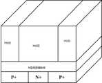
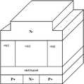
图1 为SiC Semi-SuperJunction RC-JGBT器件元胞结构示意图;Figure 1 is a schematic diagram of the cell structure of the SiC Semi-SuperJunction RC-JGBT device;
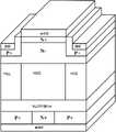
图2为本发明制作方法的流程示意图;Fig. 2 is a schematic flow sheet of the preparation method of the present invention;
图3(a)至图3(j)为本发明方法各步骤中间产物的结构示意图。Fig. 3(a) to Fig. 3(j) are structural schematic diagrams of intermediate products in each step of the method of the present invention.
具体实施方式Detailed ways
为使本申请实施例的目的、技术方案和优点更加清楚,下面将结合本申请实施例中的附图,对本申请实施例中的技术方案进行清楚、完整地描述,显然,所描述的实施例是本申请一部分实施例,而不是全部的实施例。基于本申请中的实施例,本领域普通技术人员在没有作出创造性劳动前提下所获得的全部其他实施例,都属于本申请保护的范围。In order to make the purposes, technical solutions and advantages of the embodiments of the present application clearer, the technical solutions in the embodiments of the present application will be clearly and completely described below in conjunction with the drawings in the embodiments of the present application. Obviously, the described embodiments It is a part of the embodiments of this application, not all of them. Based on the embodiments in this application, all other embodiments obtained by persons of ordinary skill in the art without creative efforts fall within the protection scope of this application.
图1 为SiC Semi-SuperJunction RC-JGBT器件元胞结构示意图。该器件的元胞结构从下到上依次为集电极Collector、P+型衬底层、设置在所述P+型衬底层中间的N+型掺杂区、N型底部辅助层N-BAL、N柱区N-pillar、设置于所述N柱区N-pillar两侧的P柱区P-pillar、N-型漂移区、设置于所述N-型漂移区两侧的P+型掺杂区、设置于两侧的P+型掺杂区之上的栅极Gate,设置于N-型漂移区上方的N+型发射极区、设置于N+型发射极区上方的发射极Emitter。Figure 1 is a schematic diagram of the cell structure of the SiC Semi-SuperJunction RC-JGBT device. The cell structure of the device is, from bottom to top, the collector collector, the P+ type substrate layer, the N+ type doped region arranged in the middle of the P+ type substrate layer, the N type bottom auxiliary layer N-BAL, and the N column region N -pillar, the P-pillar region P-pillar arranged on both sides of the N-pillar region of the N-pillar region, the N-type drift region, the P+ type doped region arranged on both sides of the N-type drift region, arranged on both sides The gate Gate above the P+ type doped region on the side, the N+ type emitter region above the N-type drift region, and the emitter Emitter above the N+ type emitter region.
该RC-JGBT器件的工作原理如下:在器件栅极加负电压,P+型掺杂区向N-型沟道区耗尽,且耗尽层随着负压绝对值升高而变宽。当耗尽层足够宽以至于扩张并完全占据N-型沟道区时,垂直沟道被夹断。此时,SiC Semi-SuperJunction RC-JGBT的集电极到发射极之间几乎没有电流流过,器件处于关断状态。在器件栅极不加电压或加正电压时,P+型掺杂区不形成展宽的耗尽层。因此,电流从集电极流向发射极,器件处于导通状态。当电流很小时,电流从衬底N+型掺杂区流向发射极,器件处于单极电子导通状态;当电流慢慢变大后,衬底P+型掺杂区开始向漂移区中注入空穴,电流同时从衬底P+型和N+型掺杂区流向发射极,器件处于双极型导通状态。The working principle of the RC-JGBT device is as follows: a negative voltage is applied to the gate of the device, and the P+ type doped region is depleted to the N-type channel region, and the depletion layer becomes wider as the absolute value of the negative voltage increases. When the depletion layer is wide enough to expand and fully occupy the N-type channel region, the vertical channel is pinched off. At this time, almost no current flows from the collector to the emitter of the SiC Semi-SuperJunction RC-JGBT, and the device is in an off state. When no voltage is applied to the gate of the device or a positive voltage is applied, the P+ type doped region does not form a widened depletion layer. Therefore, current flows from collector to emitter and the device is in conduction state. When the current is small, the current flows from the N+ doped region of the substrate to the emitter, and the device is in a unipolar electronic conduction state; when the current increases slowly, the P+ doped region of the substrate begins to inject holes into the drift region , the current flows from the P+ type and N+ type doped regions of the substrate to the emitter at the same time, and the device is in a bipolar conduction state.
图2为本发明制作方法的流程示意图,图3(a)至图3(j)为本发明方法各步骤中间产物的结构示意图。该方法包括如下步骤:Fig. 2 is a schematic flowchart of the production method of the present invention, and Fig. 3(a) to Fig. 3(j) are structural schematic diagrams of intermediate products of each step of the method of the present invention. The method comprises the steps of:
步骤1、选定待加工芯片的SiC P+型衬底;如图3(a)所示;Step 1. Select the SiC P+ substrate of the chip to be processed; as shown in Figure 3(a);
步骤2、在SiC P+型衬底上通过异质外延生长形成N型底部辅助层N-BAL;如图3(b)所示;Step 2. Form the N-type bottom auxiliary layer N-BAL on the SiC P+ type substrate by heteroepitaxial growth; as shown in Figure 3(b);
步骤3、将芯片翻转,在SiC P+型衬底上通过干法刻蚀并同质外延形成N+型掺杂区;如图3(c)所示;Step 3. Turn the chip over, and form an N+ type doped region on the SiC P+ type substrate by dry etching and homoepitaxial growth; as shown in Figure 3(c);
步骤4、将芯片翻转,在N型底部辅助层上通过同质外延生长形成N柱区N-pillar;如图3(d)所示;Step 4. Turn the chip over, and form the N-pillar in the N-pillar region by homoepitaxial growth on the N-type bottom auxiliary layer; as shown in Figure 3(d);
步骤5、在N柱区N-pillar两侧通过干法刻蚀并异质外延生长形成P柱区P-pillar;如图3(e)所示;Step 5. Form the P-pillar in the P-pillar area by dry etching and heteroepitaxial growth on both sides of the N-pillar in the N-pillar area; as shown in Figure 3(e);
步骤6、在N柱区N-pillar顶部通过同质外延生长形成N-型漂移区;如图3(f)所示;Step 6, forming an N-type drift region by homoepitaxial growth on the top of the N-pillar in the N-pillar region; as shown in Figure 3(f);
步骤7、在N-型漂移区两侧通过干法刻蚀形成栅极Gate的沟槽;如图3(g)所示;Step 7. Form gate trenches on both sides of the N-type drift region by dry etching; as shown in Figure 3(g);
步骤8、在栅极Gate的沟槽中通过Al离子垂直注入和侧向注入形成P+型参杂区;如图3(h)所示;Step 8, forming a P+ type doped region in the trench of the gate Gate by vertical implantation and lateral implantation of Al ions; as shown in Figure 3(h);
步骤9、在N-漂移区顶部通过N离子垂直注入形成N+型发射极区;如图3(i)。Step 9, forming an N+ type emitter region by vertically implanting N ions at the top of the N− drift region; as shown in Figure 3 (i).
步骤10、分别在栅极Gate的沟槽、顶部N+型发射极区、底部P+型衬底层淀积Al金属形成栅极Gate、发射极Emitter、集电极Collector;如图3(j)所示。Step 10. Deposit Al metal on the trench of the gate gate, the top N+ type emitter region, and the bottom P+ type substrate layer to form the gate gate, emitter electrode, and collector electrode Collector; as shown in Figure 3(j).
上述技术方案,通过采用半超结结构,集成反向续流二极管,沟槽型栅极结构,垂直沟道,器件的击穿电压更高,接近理想SiC材料极限的超低导通电阻,具有超高的反向恢复能力,开关速度快,器件元胞尺寸更小,设计灵活,大规模量产可以显著降低制作成本。The above technical solution adopts a semi-superjunction structure, integrates a reverse freewheeling diode, a trench gate structure, and a vertical channel. The breakdown voltage of the device is higher, and the ultra-low on-resistance close to the limit of the ideal SiC material has the advantages of Ultra-high reverse recovery capability, fast switching speed, smaller device cell size, flexible design, and large-scale mass production can significantly reduce production costs.
虽然以上描述了本发明的具体实施方式,但是本领域的技术人员应当理解,这些仅是举例说明,本发明的保护范围是由所附权利要求书限定的。本领域的技术人员在不背离本发明的原理和实质的前提下,可以对这些实施方式作出多种变更或修改,但这些变更和修改均落入本发明的保护范围。Although the specific embodiments of the present invention have been described above, those skilled in the art should understand that these are only examples, and the protection scope of the present invention is defined by the appended claims. Those skilled in the art can make various changes or modifications to these embodiments without departing from the principle and essence of the present invention, but these changes and modifications all fall within the protection scope of the present invention.
Claims (10)
Translated fromChinesePriority Applications (1)
| Application Number | Priority Date | Filing Date | Title |
|---|---|---|---|
| CN202211081098.9ACN115188814B (en) | 2022-09-06 | 2022-09-06 | RC-JGBT device and manufacturing method thereof |
Applications Claiming Priority (1)
| Application Number | Priority Date | Filing Date | Title |
|---|---|---|---|
| CN202211081098.9ACN115188814B (en) | 2022-09-06 | 2022-09-06 | RC-JGBT device and manufacturing method thereof |
Publications (2)
| Publication Number | Publication Date |
|---|---|
| CN115188814A CN115188814A (en) | 2022-10-14 |
| CN115188814Btrue CN115188814B (en) | 2023-01-20 |
Family
ID=83524066
Family Applications (1)
| Application Number | Title | Priority Date | Filing Date |
|---|---|---|---|
| CN202211081098.9AActiveCN115188814B (en) | 2022-09-06 | 2022-09-06 | RC-JGBT device and manufacturing method thereof |
Country Status (1)
| Country | Link |
|---|---|
| CN (1) | CN115188814B (en) |
Families Citing this family (2)
| Publication number | Priority date | Publication date | Assignee | Title |
|---|---|---|---|---|
| CN115241286B (en)* | 2022-09-21 | 2023-01-31 | 深圳平创半导体有限公司 | A SiC semi-superjunction junction gate bipolar transistor device and its manufacturing method |
| CN116544273A (en)* | 2023-07-07 | 2023-08-04 | 深圳平创半导体有限公司 | Reverse conduction-junction gate bipolar transistor device and manufacturing method thereof |
Citations (5)
| Publication number | Priority date | Publication date | Assignee | Title |
|---|---|---|---|---|
| GB201210369D0 (en)* | 2010-04-07 | 2012-07-25 | Ge Aviat Systems Ltd | Power switches for aircraft |
| CN112599588A (en)* | 2020-12-15 | 2021-04-02 | 陈小建 | SiC semiconductor device and method for manufacturing same |
| CN113964196A (en)* | 2021-10-20 | 2022-01-21 | 重庆平创半导体研究院有限责任公司 | A depletion mode power semiconductor structure, series structure and processing technology |
| CN113990757A (en)* | 2021-10-27 | 2022-01-28 | 电子科技大学 | A MOS device structure and manufacturing method |
| CN114613861A (en)* | 2022-05-16 | 2022-06-10 | 深圳平创半导体有限公司 | Trench SiC JFET device and preparation method thereof |
Family Cites Families (3)
| Publication number | Priority date | Publication date | Assignee | Title |
|---|---|---|---|---|
| JP5757101B2 (en)* | 2011-02-17 | 2015-07-29 | 富士電機株式会社 | Super junction semiconductor device |
| JP7446198B2 (en)* | 2020-10-01 | 2024-03-08 | 三菱電機株式会社 | semiconductor equipment |
| CN114937689B (en)* | 2022-06-06 | 2023-04-28 | 电子科技大学 | A planar SiC IGBT and its manufacturing method |
- 2022
- 2022-09-06CNCN202211081098.9Apatent/CN115188814B/enactiveActive
Patent Citations (5)
| Publication number | Priority date | Publication date | Assignee | Title |
|---|---|---|---|---|
| GB201210369D0 (en)* | 2010-04-07 | 2012-07-25 | Ge Aviat Systems Ltd | Power switches for aircraft |
| CN112599588A (en)* | 2020-12-15 | 2021-04-02 | 陈小建 | SiC semiconductor device and method for manufacturing same |
| CN113964196A (en)* | 2021-10-20 | 2022-01-21 | 重庆平创半导体研究院有限责任公司 | A depletion mode power semiconductor structure, series structure and processing technology |
| CN113990757A (en)* | 2021-10-27 | 2022-01-28 | 电子科技大学 | A MOS device structure and manufacturing method |
| CN114613861A (en)* | 2022-05-16 | 2022-06-10 | 深圳平创半导体有限公司 | Trench SiC JFET device and preparation method thereof |
Also Published As
| Publication number | Publication date |
|---|---|
| CN115188814A (en) | 2022-10-14 |
Similar Documents
| Publication | Publication Date | Title |
|---|---|---|
| TWI520337B (en) | Stepped trench type gold oxygen half field effect transistor and manufacturing method thereof | |
| CN107248533A (en) | A kind of carborundum VDMOS device and preparation method thereof | |
| CN111146274B (en) | A silicon carbide trench IGBT structure and manufacturing method thereof | |
| CN115188814B (en) | RC-JGBT device and manufacturing method thereof | |
| CN106711207B (en) | SiC junction gate bipolar transistor with vertical channel and method for making the same | |
| CN115241286B (en) | A SiC semi-superjunction junction gate bipolar transistor device and its manufacturing method | |
| CN114944421B (en) | Trench type silicon carbide insulated gate field effect transistor and manufacturing method thereof | |
| CN116387362A (en) | HJD integrated SiC UMOSFET device and preparation method thereof | |
| CN114551586B (en) | Silicon carbide split gate MOSFET cell with integrated gated diode and preparation method | |
| CN114823911A (en) | Groove silicon carbide MOSFET integrated with high-speed freewheeling diode and preparation method | |
| CN117038732A (en) | Wide bandgap semiconductor trench MOSFET device and manufacturing method thereof | |
| CN105161533A (en) | Silicon carbide VDMOS device and manufacturing method | |
| CN109920838B (en) | A trench type silicon carbide MOSFET device and preparation method thereof | |
| CN117080269A (en) | Silicon carbide MOSFET device and preparation method thereof | |
| CN116364778A (en) | A SiC VDMOSFET device with integrated HJD and its preparation method | |
| CN113725280A (en) | Super-junction RB-IGBT device with low turn-on voltage | |
| CN116110796A (en) | Silicon carbide SGT-MOSFET with integrated SBD and its preparation method | |
| CN116230545A (en) | UMOSFET embedded with 3C/4H-SiC heterogeneous freewheel junction and graded semi-super junction and preparation method thereof | |
| CN103956381A (en) | MOS grid-control thyristor | |
| CN110190128A (en) | MOSFET device with silicon carbide double-sided deep L-shaped base structure and its preparation method | |
| CN106783987A (en) | The SiC Schottky gates bipolar transistor and preparation method of a kind of longitudinal channel | |
| CN103928321A (en) | Preparation method for silicon carbide insulated gate bipolar transistor | |
| CN116544273A (en) | Reverse conduction-junction gate bipolar transistor device and manufacturing method thereof | |
| CN215342616U (en) | Deep schottky power device with buried layer structure | |
| CN116169159B (en) | A super-junction insulated gate bipolar transistor structure and its manufacturing method |
Legal Events
| Date | Code | Title | Description |
|---|---|---|---|
| PB01 | Publication | ||
| PB01 | Publication | ||
| SE01 | Entry into force of request for substantive examination | ||
| SE01 | Entry into force of request for substantive examination | ||
| GR01 | Patent grant | ||
| GR01 | Patent grant |