CN115188354A - Passive Buzzer Control IC - Google Patents
Passive Buzzer Control ICDownload PDFInfo
- Publication number
- CN115188354A CN115188354ACN202210798729.2ACN202210798729ACN115188354ACN 115188354 ACN115188354 ACN 115188354ACN 202210798729 ACN202210798729 ACN 202210798729ACN 115188354 ACN115188354 ACN 115188354A
- Authority
- CN
- China
- Prior art keywords
- transistor
- circuit
- resistor
- collector
- twenty
- Prior art date
- Legal status (The legal status is an assumption and is not a legal conclusion. Google has not performed a legal analysis and makes no representation as to the accuracy of the status listed.)
- Granted
Links
Images


Classifications
- G—PHYSICS
- G10—MUSICAL INSTRUMENTS; ACOUSTICS
- G10K—SOUND-PRODUCING DEVICES; METHODS OR DEVICES FOR PROTECTING AGAINST, OR FOR DAMPING, NOISE OR OTHER ACOUSTIC WAVES IN GENERAL; ACOUSTICS NOT OTHERWISE PROVIDED FOR
- G10K9/00—Devices in which sound is produced by vibrating a diaphragm or analogous element, e.g. fog horns, vehicle hooters or buzzers
- G10K9/12—Devices in which sound is produced by vibrating a diaphragm or analogous element, e.g. fog horns, vehicle hooters or buzzers electrically operated
- G—PHYSICS
- G10—MUSICAL INSTRUMENTS; ACOUSTICS
- G10K—SOUND-PRODUCING DEVICES; METHODS OR DEVICES FOR PROTECTING AGAINST, OR FOR DAMPING, NOISE OR OTHER ACOUSTIC WAVES IN GENERAL; ACOUSTICS NOT OTHERWISE PROVIDED FOR
- G10K9/00—Devices in which sound is produced by vibrating a diaphragm or analogous element, e.g. fog horns, vehicle hooters or buzzers
- G10K9/18—Details, e.g. bulbs, pumps, pistons, switches or casings
- H—ELECTRICITY
- H02—GENERATION; CONVERSION OR DISTRIBUTION OF ELECTRIC POWER
- H02J—CIRCUIT ARRANGEMENTS OR SYSTEMS FOR SUPPLYING OR DISTRIBUTING ELECTRIC POWER; SYSTEMS FOR STORING ELECTRIC ENERGY
- H02J7/00—Circuit arrangements for charging or depolarising batteries or for supplying loads from batteries
- H02J7/0068—Battery or charger load switching, e.g. concurrent charging and load supply
- H—ELECTRICITY
- H02—GENERATION; CONVERSION OR DISTRIBUTION OF ELECTRIC POWER
- H02J—CIRCUIT ARRANGEMENTS OR SYSTEMS FOR SUPPLYING OR DISTRIBUTING ELECTRIC POWER; SYSTEMS FOR STORING ELECTRIC ENERGY
- H02J7/00—Circuit arrangements for charging or depolarising batteries or for supplying loads from batteries
- H02J7/007—Regulation of charging or discharging current or voltage
- H02J7/00712—Regulation of charging or discharging current or voltage the cycle being controlled or terminated in response to electric parameters
- H02J7/00714—Regulation of charging or discharging current or voltage the cycle being controlled or terminated in response to electric parameters in response to battery charging or discharging current
- H—ELECTRICITY
- H02—GENERATION; CONVERSION OR DISTRIBUTION OF ELECTRIC POWER
- H02J—CIRCUIT ARRANGEMENTS OR SYSTEMS FOR SUPPLYING OR DISTRIBUTING ELECTRIC POWER; SYSTEMS FOR STORING ELECTRIC ENERGY
- H02J7/00—Circuit arrangements for charging or depolarising batteries or for supplying loads from batteries
- H02J7/007—Regulation of charging or discharging current or voltage
- H02J7/00712—Regulation of charging or discharging current or voltage the cycle being controlled or terminated in response to electric parameters
- H02J7/007182—Regulation of charging or discharging current or voltage the cycle being controlled or terminated in response to electric parameters in response to battery voltage
Landscapes
- Engineering & Computer Science (AREA)
- Power Engineering (AREA)
- Physics & Mathematics (AREA)
- Acoustics & Sound (AREA)
- Multimedia (AREA)
- Amplifiers (AREA)
Abstract
Translated fromChinese
Description
Translated fromChinese技术领域technical field
本申请涉及电路领域,尤其涉及一种无源蜂鸣器控制集成电路。The present application relates to the field of circuits, and in particular, to a passive buzzer control integrated circuit.
背景技术Background technique
音乐蜂鸣器电路是一种使用扬声器实现音乐功能的电路,该电路广泛应用于洗衣机,电冰箱,热水器,咖啡机等。The music buzzer circuit is a circuit that uses a speaker to realize the music function, which is widely used in washing machines, refrigerators, water heaters, coffee machines, etc.
传统的音乐蜂鸣器电路通常采用三极管,电阻,电容等等分立器件搭建,在生产过程中容易受到分立器件精度、可靠性等级等因素的制约,并且分立器件较多,导致PCB面积占用大。Traditional music buzzer circuits are usually built with discrete devices such as transistors, resistors, capacitors, etc., which are easily restricted by factors such as the accuracy and reliability of discrete devices in the production process, and there are many discrete devices, resulting in a large PCB area.
发明内容SUMMARY OF THE INVENTION
本申请提供一种无源蜂鸣器控制集成电路,用以实现电路集成化效果,减少PCB面积,摆脱分立器件精度、可靠性等级等因素的制约。The present application provides a passive buzzer control integrated circuit, which is used to realize the effect of circuit integration, reduce the PCB area, and get rid of the constraints of discrete device precision, reliability level and other factors.
一方面,本申请提供一种无源蜂鸣器控制集成电路,包括:使能电路、偏置电路、充放电电路、电平转换电路以及驱动电路;其中,In one aspect, the present application provides a passive buzzer control integrated circuit, including: an enabling circuit, a bias circuit, a charging and discharging circuit, a level conversion circuit and a driving circuit; wherein,
所述使能电路,用于根据使能信号输出充电电流和启动电流;所述偏置电路,与所述使能电路和所述充放电电路连接,用于根据所述启动电流输出放电电流;the enabling circuit is used for outputting the charging current and the starting current according to the enabling signal; the bias circuit is connected with the enabling circuit and the charging and discharging circuit and is used for outputting the discharging current according to the starting current;
所述充放电电路,与所述使能电路连接,用于基于所述充电电流和所述放电电流,输出初始电压;所述电平转换电路,与所述充放电电路连接,用于对所述初始电压进行变压处理后,输出供电电压;The charging and discharging circuit is connected to the enabling circuit for outputting an initial voltage based on the charging current and the discharging current; the level conversion circuit is connected to the charging and discharging circuit for After the initial voltage is transformed, the power supply voltage is output;
所述驱动电路,与所述电平转换电路和扬声器连接,用于基于所述供电电压和调制控制信号,向所述扬声器输出驱动信号,以驱动所述扬声器工作。The drive circuit is connected to the level conversion circuit and the speaker, and is configured to output a drive signal to the speaker based on the power supply voltage and the modulation control signal, so as to drive the speaker to work.
在一种实施例中,所述使能电路包括第一晶体管、第一电阻、第二电阻和偏置电流模块;In one embodiment, the enabling circuit includes a first transistor, a first resistor, a second resistor and a bias current module;
所述第一电阻的第一端用于接收所述使能信号,所述第一电阻的第二端与所述第一晶体管的基极连接;The first end of the first resistor is used to receive the enable signal, and the second end of the first resistor is connected to the base of the first transistor;
所述第一晶体管的集电极与所述充放电电路连接,用于输出所述充电电流;所述第一晶体管的发射极与所述第二电阻的第一端连接,所述第二电阻的第二端接地;The collector of the first transistor is connected to the charging and discharging circuit for outputting the charging current; the emitter of the first transistor is connected to the first end of the second resistor, and the second resistor is The second terminal is grounded;
所述偏置电流模块,与所述第一晶体管的基极连接,用于生成所述启动电流。The bias current module is connected to the base of the first transistor and is used for generating the startup current.
在一种实施例中,所述偏置电流模块包括:第二晶体管、第三晶体管、第四晶体管与第三电阻;In one embodiment, the bias current module includes: a second transistor, a third transistor, a fourth transistor and a third resistor;
所述第二晶体管的基极与所述第二晶体管的集电极和所述第一晶体管的基极连接,所述第二晶体管的发射极与所述第三电阻的第一端和所述第三晶体管的基极连接;The base of the second transistor is connected to the collector of the second transistor and the base of the first transistor, and the emitter of the second transistor is connected to the first terminal of the third resistor and the first terminal of the first transistor. The base connection of the three transistors;
所述第三电阻的第二端与所述第三晶体管的集电极连接,所述第三晶体管的发射极接地;The second end of the third resistor is connected to the collector of the third transistor, and the emitter of the third transistor is grounded;
所述第四晶体管的基极与所述第三晶体管的集电极连接;所述第四晶体管的集电极与所述偏置电路相连,用于输出所述启动电流;所述第四晶体管的发射极接地。The base of the fourth transistor is connected to the collector of the third transistor; the collector of the fourth transistor is connected to the bias circuit for outputting the startup current; the emission of the fourth transistor pole ground.
在一种实施例中,所述偏置电路包括自偏置电流镜电路。In one embodiment, the bias circuit includes a self-biased current mirror circuit.
在一种实施例中,所述自偏置电流镜电路包括:第五晶体管、第六晶体管、第七晶体管、第八晶体管、第九晶体管与第四电阻;In one embodiment, the self-biased current mirror circuit includes: a fifth transistor, a sixth transistor, a seventh transistor, an eighth transistor, a ninth transistor, and a fourth resistor;
所述第五晶体管的发射极与所述第六晶体管的发射极和所述第九晶体管的发射极连接并且接至电源;所述第五晶体管的基极与所述第五晶体管的集电极连接;所述第五晶体管的集电极与所述第七晶体管的集电极和所述使能电路连接,用于接收所述启动电流;The emitter of the fifth transistor is connected to the emitter of the sixth transistor and the emitter of the ninth transistor and is connected to the power supply; the base of the fifth transistor is connected to the collector of the fifth transistor ; the collector of the fifth transistor is connected to the collector of the seventh transistor and the enabling circuit for receiving the startup current;
所述第七晶体管的基极与所述第八晶体管的基极连接,所述第七晶体管的发射极与所述第四电阻的第一端连接,所述第四电阻的第二端接地;The base of the seventh transistor is connected to the base of the eighth transistor, the emitter of the seventh transistor is connected to the first end of the fourth resistor, and the second end of the fourth resistor is grounded;
所述第六晶体管的基极与所述第五晶体管的基极连接,所述第六晶体管的集电极与所述第八晶体管的集电极连接;所述第八晶体管的基极与所述第八晶体管的集电极连接,所述第八晶体管的发射极接地;The base of the sixth transistor is connected to the base of the fifth transistor, the collector of the sixth transistor is connected to the collector of the eighth transistor; the base of the eighth transistor is connected to the The collectors of the eight transistors are connected, and the emitters of the eighth transistors are grounded;
所述第九晶体管的基极与所述第五晶体管的基极连接,所述第九晶体管的集电极与所述充放电电路连接,用于输出放电电流。The base of the ninth transistor is connected to the base of the fifth transistor, and the collector of the ninth transistor is connected to the charge-discharge circuit for outputting a discharge current.
在一种实施例中,所述充放电电路包括:电容、放电模块和充电模块;其中,所述充电模块包括第十晶体管与第十一晶体管;所述放电模块包括第十二晶体管与第十三晶体管;In an embodiment, the charging and discharging circuit includes: a capacitor, a discharging module and a charging module; wherein the charging module includes a tenth transistor and an eleventh transistor; the discharging module includes a twelfth transistor and a tenth transistor three transistors;
所述第十晶体管的发射极与所述第十一晶体管的发射极连接并且接至电源,所述第十晶体管的基极与所述第十晶体管的集电极和所述使能电路连接,用于接收充电电流;The emitter of the tenth transistor is connected to the emitter of the eleventh transistor and is connected to the power supply, the base of the tenth transistor is connected to the collector of the tenth transistor and the enabling circuit, using to receive charging current;
所述第十一晶体管的基极与所述第十晶体管的基极连接,所述第十一晶体管的集电极与所述电容的第一端连接,所述电容的第二端接地;The base of the eleventh transistor is connected to the base of the tenth transistor, the collector of the eleventh transistor is connected to the first end of the capacitor, and the second end of the capacitor is grounded;
所述第十二晶体管的集电极与所述电容的第一端连接,所述第十二晶体管的发射极接地,所述第十二晶体管的基极与所述第十三晶体管的基极连接;所述第十三晶体管的基极与所述第十三晶体管的集电极和所述偏置电路连接,用于接收放电电流;所述第十三晶体管的发射极接地。The collector of the twelfth transistor is connected to the first end of the capacitor, the emitter of the twelfth transistor is grounded, and the base of the twelfth transistor is connected to the base of the thirteenth transistor ; the base of the thirteenth transistor is connected to the collector of the thirteenth transistor and the bias circuit for receiving discharge current; the emitter of the thirteenth transistor is grounded.
在一种实施例中,所述充放电电路还包括:分压模块以及阶梯镜像支路:In an embodiment, the charging and discharging circuit further includes: a voltage divider module and a ladder mirror branch:
所述分压模块用于输出阶梯电压,所述阶梯电压与所述阶梯镜像支路之间一一对应;The voltage dividing module is used for outputting a stepped voltage, and the stepped voltage is in one-to-one correspondence with the stepped mirror branch;
所述阶梯镜像支路,连接至对应的阶梯电压,用于根据电容的当前储能和所述阶梯电压之间的关系,启动或停止对所述电容的放电。The ladder mirror branch is connected to the corresponding ladder voltage, and is used for starting or stopping the discharge of the capacitor according to the relationship between the current energy storage of the capacitor and the ladder voltage.
在一种实施例中,所述阶梯镜像支路的数量为两个,所述阶梯电压的数量也为两个,不同阶梯镜像支路对应的阶梯电压不同。In an embodiment, the number of the ladder mirror branches is two, the number of ladder voltages is also two, and the ladder voltages corresponding to different ladder mirror branches are different.
在一种实施例中,第一阶梯镜像支路包括:第十四晶体管和第十五晶体管,第二阶梯镜像支路包括:第十六晶体管和第十七晶体管;In an embodiment, the first ladder mirror branch includes: a fourteenth transistor and a fifteenth transistor, and the second ladder mirror branch includes: a sixteenth transistor and a seventeenth transistor;
所述第十四晶体管与所述第十六晶体管互为镜像,所述第十五晶体管与所述第十七晶体管互为镜像。The fourteenth transistor and the sixteenth transistor are mirror images of each other, and the fifteenth transistor and the seventeenth transistor are mirror images of each other.
所述第十四晶体管的基极与所述第十四晶体管的集电极连接;所述第十四晶体管的集电极与所述第十五晶体管的集电极和所述分压电路连接,用于接收对应的阶梯电压;所述第十四晶体管的发射极与所述电容的第一端连接;The base of the fourteenth transistor is connected to the collector of the fourteenth transistor; the collector of the fourteenth transistor is connected to the collector of the fifteenth transistor and the voltage divider circuit, for receiving the corresponding step voltage; the emitter of the fourteenth transistor is connected to the first end of the capacitor;
所述第十五晶体管的基极与所述第十三晶体管的基极连接,所述第十五晶体管的发射极接地;The base of the fifteenth transistor is connected to the base of the thirteenth transistor, and the emitter of the fifteenth transistor is grounded;
所述第十四晶体管与所述第十六晶体管互为镜像,所述第十五晶体管与所述第十七晶体管互为镜像。The fourteenth transistor and the sixteenth transistor are mirror images of each other, and the fifteenth transistor and the seventeenth transistor are mirror images of each other.
在一种实施例中,所述第十四晶体管的集电极和所述分压电路之间设置有单向导通元件;In an embodiment, a unidirectional conduction element is arranged between the collector of the fourteenth transistor and the voltage divider circuit;
所述单向导通元件的第一端与所述分压电路连接,所述单向导通元件的第二端与所述第十四晶体管的集电极连接,用于将所述分压电路提供的阶梯电压单向传输至所述第十四晶体管。The first end of the one-way conduction element is connected to the voltage divider circuit, and the second end of the one-way conduction element is connected to the collector of the fourteenth transistor for connecting the voltage provided by the voltage divider circuit. The stepped voltage is unidirectionally transmitted to the fourteenth transistor.
在一种实施例中,所述单向导通元件包括:第十八晶体管与第十九晶体管;In an embodiment, the unidirectional conduction element includes: an eighteenth transistor and a nineteenth transistor;
所述第十八晶体管的发射极与所述分压电路连接,所述第十八晶体管的基极与所述第十八晶体管的集电极连接,所述第十八晶体管的集电极与所述第十四晶体管的集电极连接;The emitter of the eighteenth transistor is connected to the voltage divider circuit, the base of the eighteenth transistor is connected to the collector of the eighteenth transistor, and the collector of the eighteenth transistor is connected to the the collector connection of the fourteenth transistor;
所述第十八晶体管与所述第十九晶体管互为镜像。The eighteenth transistor and the nineteenth transistor are mirror images of each other.
在一种实施例中,所述单向导通元件包括:二极管;In one embodiment, the one-way conducting element comprises: a diode;
所述二极管的正极与所述分压电路连接,所述二极管的负极与所述第十四晶体管的集电极连接。The anode of the diode is connected to the voltage divider circuit, and the cathode of the diode is connected to the collector of the fourteenth transistor.
在一种实施例中,所述分压模块包括:第二十晶体管、第五电阻、第六电阻、第七电阻以及第八电阻;In an embodiment, the voltage dividing module includes: a twentieth transistor, a fifth resistor, a sixth resistor, a seventh resistor, and an eighth resistor;
所述第五电阻的第一端接接至电源;所述第五电阻的第二端用于输出第一阶梯电压,所述第五电阻的第二端与所述第六电阻的第一端以及所述第一阶梯电压对应的阶梯镜像支路中的第十四晶体管的集电极连接;The first end of the fifth resistor is connected to the power supply; the second end of the fifth resistor is used to output the first step voltage, the second end of the fifth resistor and the first end of the sixth resistor and the collector connection of the fourteenth transistor in the step mirror branch corresponding to the first step voltage;
所述第六电阻的第二端用于输出第二阶梯电压,所述第六电阻的第二端与所述第七电阻的第一端以及所述第二阶梯电压对应的阶梯镜像支路中的第十四晶体管的集电极连接;The second end of the sixth resistor is used to output the second step voltage, and the second end of the sixth resistor is in the step mirror branch corresponding to the first end of the seventh resistor and the second step voltage. The collector connection of the fourteenth transistor;
所述第七电阻的第二端与所述第二十晶体管的集电极连接,所述第二十晶体管的第二端接地;所述第八电阻的第一端与所述电平转换电路连接,用于接收所述供电电压;所述第八电阻的第二端与所述第二十晶体管的基极连接。The second end of the seventh resistor is connected to the collector of the twentieth transistor, and the second end of the twentieth transistor is grounded; the first end of the eighth resistor is connected to the level conversion circuit , for receiving the supply voltage; the second end of the eighth resistor is connected to the base of the twentieth transistor.
在一种实施例中,所述驱动电路包括:第二十一晶体管、第二十二晶体管、第二十三晶体管、第二十四晶体管、第二十五晶体管、第二十六晶体管、第九电阻、第十电阻、第十一电阻以及第十二电阻;In an embodiment, the driving circuit includes: a twenty-first transistor, a twenty-second transistor, a twenty-third transistor, a twenty-fourth transistor, a twenty-fifth transistor, a twenty-sixth transistor, a Nine resistors, tenth resistors, eleventh resistors and twelfth resistors;
所述第二十一晶体管的发射极与所述第九电阻的第一端和所述第二十二晶体管的发射极连接且连至所述供电电压,所述第二十一晶体管的基极与所述第九电阻的第二端连接;所述第二十一晶体管的集电极与所述第二十四晶体管的集电极连接,用于输出所述驱动信号;所述第二十四晶体管的发射极接地;The emitter of the twenty-first transistor is connected to the first end of the ninth resistor and the emitter of the twenty-second transistor and is connected to the supply voltage, and the base of the twenty-first transistor connected to the second end of the ninth resistor; the collector of the twenty-first transistor is connected to the collector of the twenty-fourth transistor for outputting the drive signal; the twenty-fourth transistor The emitter is grounded;
所述第二十二晶体管的发射极与所述第十电阻的第一端连接,所述第二十二晶体管的基极与所述第十电阻的第二端连接;所述第二十二晶体管的集电极与所述第二十三晶体管的集电极连接,用于输出所述驱动信号;所述第二十三晶体管的发射极接地;The emitter of the twenty-second transistor is connected to the first end of the tenth resistor, and the base of the twenty-second transistor is connected to the second end of the tenth resistor; the twenty-second transistor is connected to the second end of the tenth resistor. The collector of the transistor is connected to the collector of the twenty-third transistor for outputting the driving signal; the emitter of the twenty-third transistor is grounded;
所述第十一电阻的第一端与所述二十五晶体管的基极连接,用于接收所述调制控制信号;所述第十一电阻的第二端与所述第二十三晶体管的基极连接;所述第二十五晶体管的集电极与所述第九电阻的第二端连接,所述第二十五晶体管的发射极接地;The first end of the eleventh resistor is connected to the base of the twenty-fifth transistor for receiving the modulation control signal; the second end of the eleventh resistor is connected to the second end of the twenty-third transistor. the base is connected; the collector of the twenty-fifth transistor is connected to the second end of the ninth resistor, and the emitter of the twenty-fifth transistor is grounded;
所述第十二电阻的第一端与所述第二十四晶体管的基极连接;所述第十二电阻的第二端与所述第二十六晶体管的基极连接,用于接收所述调制控制信号的反相信号;所述第二十六晶体管的集电极与所述第十电阻的第二端连接,所述第二十六晶体管的发射极接地。The first end of the twelfth resistor is connected to the base of the twenty-fourth transistor; the second end of the twelfth resistor is connected to the base of the twenty-sixth transistor for receiving all the The inversion signal of the modulation control signal; the collector of the twenty-sixth transistor is connected to the second end of the tenth resistor, and the emitter of the twenty-sixth transistor is grounded.
在一种实施例中,所述驱动电路还包括:反相器;In one embodiment, the driving circuit further includes: an inverter;
所述反相器的输入端连至所述调制控制信号,所述反相器的输出端与所述第二十六晶体管的基极连接。The input terminal of the inverter is connected to the modulation control signal, and the output terminal of the inverter is connected to the base of the twenty-sixth transistor.
本申请提供的无源蜂鸣器控制集成电路,包括:使能电路、偏置电路、充放电电路、电平转换电路以及驱动电路。所述使能电路,用于根据使能信号输出充电电流和启动电流;所述偏置电路,与所述使能电路和所述充放电电路连接,用于根据所述启动电流输出放电电流;所述充放电电路,与所述使能电路连接,用于基于所述充电电流和所述放电电流,输出初始电压;所述电平转换电路,与所述充放电电路连接,用于对所述初始电压进行变压处理后,输出供电电压;所述驱动电路,与所述电平转换电路和扬声器连接,用于基于所述供电电压和调制控制信号,向所述扬声器输出驱动信号,以驱动所述扬声器工作。本申请提供的方案采用集成电路的设计思维,将音乐无源蜂鸣器控制电路达到集成化效果,从而减少了PCB面积,摆脱了分立器件精度、可靠性等级等因素的制约。The passive buzzer control integrated circuit provided by the present application includes an enabling circuit, a bias circuit, a charging and discharging circuit, a level conversion circuit and a driving circuit. the enabling circuit is used for outputting the charging current and the starting current according to the enabling signal; the bias circuit is connected with the enabling circuit and the charging and discharging circuit and is used for outputting the discharging current according to the starting current; The charging and discharging circuit is connected to the enabling circuit for outputting an initial voltage based on the charging current and the discharging current; the level conversion circuit is connected to the charging and discharging circuit for After the initial voltage is transformed, the power supply voltage is output; the drive circuit is connected to the level conversion circuit and the speaker, and is used for outputting a drive signal to the speaker based on the power supply voltage and the modulation control signal, so as to drive the speaker to work. The solution provided in this application adopts the design thinking of integrated circuits, and achieves the integrated effect of the control circuit of the passive music buzzer, thereby reducing the PCB area and getting rid of the constraints of discrete device precision, reliability level and other factors.
附图说明Description of drawings
此处的附图被并入说明书中并构成本说明书的一部分,示出了符合本申请的实施例,并与说明书一起用于解释本申请的原理。The accompanying drawings, which are incorporated in and constitute a part of this specification, illustrate embodiments consistent with the application and together with the description serve to explain the principles of the application.
图1为无源蜂鸣器控制集成电路控制扬声器工作的示意图;1 is a schematic diagram of a passive buzzer control integrated circuit controlling the operation of a loudspeaker;
图2为本申请实施例一提供的无源蜂鸣器控制集成电路的结构示意图;FIG. 2 is a schematic structural diagram of a passive buzzer control integrated circuit provided in Embodiment 1 of the present application;
图3为本申请实施例一提供的是使能电路的结构示意图;3 is a schematic structural diagram of an enabling circuit provided in Embodiment 1 of the present application;
图4为本申请实施例一提供的是使能电路的另一种结构示意图;4 is another schematic structural diagram of an enabling circuit provided in Embodiment 1 of the present application;
图5为本申请实施例一提供的偏置电路的结构示意图;FIG. 5 is a schematic structural diagram of a bias circuit provided in Embodiment 1 of the present application;
图6为本申请实施例一提供的偏置电路的另一种结构示意图;FIG. 6 is another schematic structural diagram of the bias circuit provided in Embodiment 1 of the present application;
图7为本申请实施例一提供的充放电电路的结构示意图;FIG. 7 is a schematic structural diagram of a charging and discharging circuit provided in Embodiment 1 of the present application;
图8为本申请实施例一提供的充放电电路的另一种结构示意图;FIG. 8 is another schematic structural diagram of the charging and discharging circuit provided in Embodiment 1 of the present application;
图9为本申请实施例一提供的充放电电路的又一种结构示意图;FIG. 9 is another schematic structural diagram of the charging and discharging circuit provided in Embodiment 1 of the present application;
图10为本申请实施例一提供的充放电电路的又一种结构示意图;FIG. 10 is another schematic structural diagram of the charging and discharging circuit provided in Embodiment 1 of the present application;
图11为本申请实施例一提供的充放电电路的又一种结构示意图;11 is another schematic structural diagram of the charging and discharging circuit provided in Embodiment 1 of the present application;
图12为本申请实施例一提供的充放电电路的又一种结构示意图;12 is another schematic structural diagram of the charging and discharging circuit provided in Embodiment 1 of the present application;
图13为本申请实施例一提供的充放电电路的又一种结构示意图;13 is another schematic structural diagram of the charging and discharging circuit provided in Embodiment 1 of the present application;
图14为本申请实施例一提供的驱动电路的结构示意图;14 is a schematic structural diagram of a driving circuit provided in Embodiment 1 of the present application;
图15为本申请实施例一提供的驱动电路的另一种结构示意图。FIG. 15 is another schematic structural diagram of the driving circuit provided in Embodiment 1 of the present application.
附图标记说明:Description of reference numbers:
21:使能电路;21: enable circuit;
22:偏置电路;22: Bias circuit;
23:充放电电路;23: charge and discharge circuit;
24:电平转换电路;24: level conversion circuit;
25:驱动电路;25: drive circuit;
Q1:第一晶体管;Q1: the first transistor;
Q2:第二晶体管;Q2: the second transistor;
Q3:第三晶体管;Q3: the third transistor;
Q4:第四晶体管;Q4: the fourth transistor;
Q5:第五晶体管;Q5: fifth transistor;
Q6:第六晶体管;Q6: sixth transistor;
Q7:第七晶体管;Q7: seventh transistor;
Q8:第八晶体管;Q8: the eighth transistor;
Q9:第九晶体管;Q9: the ninth transistor;
Q10:第十晶体管;Q10: Tenth transistor;
Q11:第十一晶体管;Q11: the eleventh transistor;
Q12:第十二晶体管;Q12: the twelfth transistor;
Q13:第十三晶体管;Q13: Thirteenth transistor;
Q14:第十四晶体管;Q14: the fourteenth transistor;
Q15:第十五晶体管;Q15: the fifteenth transistor;
Q16:第十六晶体管;Q16: the sixteenth transistor;
Q17:第十七晶体管;Q17: the seventeenth transistor;
Q18:第十八晶体管;Q18: Eighteenth transistor;
Q19:第十九晶体管;Q19: The nineteenth transistor;
Q20:第二十晶体管;Q20: the twentieth transistor;
Q21:第二十一晶体管;Q21: the twenty-first transistor;
Q22:第二十二晶体管;Q22: the twenty-second transistor;
Q23:第二十三晶体管;Q23: the twenty-third transistor;
Q24:第二十四晶体管;Q24: the twenty-fourth transistor;
Q25:第二十五晶体管;Q25: the twenty-fifth transistor;
Q26:第二十六晶体管;Q26: the twenty-sixth transistor;
R1:第一电阻;R1: the first resistance;
R2:第二电阻;R2: the second resistance;
R3:第三电阻;R3: the third resistor;
R4:第四电阻;R4: the fourth resistor;
R5:第五电阻;R5: fifth resistor;
R6:第六电阻;R6: sixth resistor;
R7:第七电阻;R7: seventh resistor;
R8:第八电阻;R8: the eighth resistor;
R9:第九电阻;R9: ninth resistor;
R10:第十电阻;R10: tenth resistance;
R11:第十一电阻;R11: the eleventh resistor;
R12:第十二电阻。R12: Twelfth resistor.
具体实施方式Detailed ways
这里将详细地对示例性实施例进行说明,其示例表示在附图中。下面的描述涉及附图时,除非另有表示,不同附图中的相同数字表示相同或相似的要素。以下示例性实施例中所描述的实施方式并不代表与本申请相一致的所有实施方式。相反,它们仅是与如所附权利要求书中所详述的、本申请的一些方面相一致的装置和方法的例子。Exemplary embodiments will be described in detail herein, examples of which are illustrated in the accompanying drawings. Where the following description refers to the drawings, the same numerals in different drawings refer to the same or similar elements unless otherwise indicated. The implementations described in the illustrative examples below are not intended to represent all implementations consistent with this application. Rather, they are merely examples of apparatus and methods consistent with some aspects of the present application as recited in the appended claims.
需要说明的是,本申请中对于术语的简要说明,仅是为了方便理解接下来描述的实施方式,而不是意图限定本申请的实施方式。除非另有说明,这些术语应当按照其普通和通常的含义理解。It should be noted that the brief description of the terms in the present application is only for the convenience of understanding the embodiments described below, rather than intended to limit the embodiments of the present application. Unless otherwise specified, these terms are to be understood according to their ordinary and ordinary meanings.
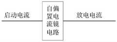
在实际应用中,蜂鸣器集成电路主要是一种使用扬声器实现音乐功能的电路,如图1所示,图1为无源蜂鸣器控制集成电路控制扬声器工作的示意图,通常情况下,广泛应用于洗衣机,电冰箱,热水器,咖啡机等。由图可知,所述无源蜂鸣器控制集成电路将输入信号转化为输出信号发送给扬声器,使得扬声器发声工作,在一种示例中,本申请提供的无源蜂鸣器控制集成电路也可改变发送的信号频率改变扬声器的声调变化,使得扬声器的声音更加悦耳。In practical applications, the buzzer integrated circuit is mainly a circuit that uses speakers to achieve music functions, as shown in Figure 1. Figure 1 is a schematic diagram of the passive buzzer control integrated circuit controlling the operation of the speaker. Used in washing machines, refrigerators, water heaters, coffee machines, etc. It can be seen from the figure that the passive buzzer control integrated circuit converts the input signal into an output signal and sends it to the speaker, so that the speaker works. In an example, the passive buzzer control integrated circuit provided by the present application can also Changing the frequency of the transmitted signal changes the tone of the speaker, making the speaker sound more pleasing to the ear.
下面以具体的实施例对本申请的技术方案以及本申请的技术方案进行详细说明。下面这几个具体的实施例可以相互结合,对于相同或相似的概念或过程可能在某些实施例中不再赘述。在本申请的描述中,除非另有明确的规定和限定,各术语应在本领域内做广义理解。下面将结合附图,对本申请的实施例进行描述。The technical solutions of the present application and the technical solutions of the present application will be described in detail below with specific embodiments. The following specific embodiments may be combined with each other, and the same or similar concepts or processes may not be repeated in some embodiments. In the description of the present application, unless otherwise clearly defined and defined, each term should be understood broadly in the art. The embodiments of the present application will be described below with reference to the accompanying drawings.
实施例一Example 1
图2为本申请实施例一提供的无源蜂鸣器控制集成电路的结构示意图,如图2所示,所述无源蜂鸣器控制集成电路包括:使能电路21、偏置电路22、充放电电路23、电平转换电路24以及驱动电路25;其中,FIG. 2 is a schematic structural diagram of the passive buzzer control integrated circuit provided in the first embodiment of the application. As shown in FIG. 2 , the passive buzzer control integrated circuit includes: an enabling
使能电路21,用于根据使能信号输出充电电流和启动电流;偏置电路22,与使能电路21和充放电电路23连接,用于根据所述启动电流输出放电电流;The enabling
充放电电路23,与使能电路21连接,用于基于所述充电电流和所述放电电流,输出初始电压;电平转换电路24与充放电电路23连接,用于对所述初始电压进行变压处理后,输出供电电压;The charging and discharging
驱动电路25,与电平转换电路24和扬声器连接,用于基于所述供电电压和调制控制信号,向所述扬声器输出驱动信号,以驱动所述扬声器工作。The
结合场景示例,所述无源蜂鸣器控制集成电路在使能信号的接入后开始工作,使能电路21接收所述使能信号后输出启动电流提供给偏置电路22,同时输出一个充电电流提供给充放电电路23。偏置电路22接收到所述启动电流后,输出放电电流提供给充放电电路23。充放电电路接收到所述充电电流与所述放电电流后,输出一个初始电压提供给电平转换电路24,电平转换电路24会对接收到的初始电压进行电平转换,生成供电电压VREG提供给驱动电路25。驱动电路25接收到所述供电电压后,基于调制控制信号生成驱动信号提供给扬声器,从而控制扬声器工作,所述调制控制信号是一种脉宽调制PWM信号,是扬声器频率输入信号。作为示例,供电电压VREG还可以返回充放电电路23。Combined with the example of the scene, the passive buzzer control integrated circuit starts to work after the enable signal is connected, the enable
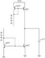
在一个示例中,图3为本申请实施例一提供的使能电路的结构示意图,使能电路21包括第一晶体管Q1、第一电阻R1、第二电阻R2和偏置电流模块;In an example, FIG. 3 is a schematic structural diagram of an enabling circuit provided in Embodiment 1 of the present application, and the enabling
第一电阻R1的第一端用于接收所述使能信号,第一电阻R1的第二端与第一晶体管Q1的基极连接;The first end of the first resistor R1 is used to receive the enable signal, and the second end of the first resistor R1 is connected to the base of the first transistor Q1;
第一晶体管Q1的集电极与所述充放电电路23连接,用于输出所述充电电流;第一晶体管Q1的发射极与第二电阻R2的第一端连接,第二电阻R2的第二端接地;The collector of the first transistor Q1 is connected to the charging and discharging
所偏置电流模块,与第一晶体管Q1的基极连接,用于生成所述启动电流。The bias current module is connected to the base of the first transistor Q1, and is used for generating the startup current.
使能电路21是由第一电阻R1、第二电阻R2、第一晶体管与第一镜像电路都构成的。使能信号通过第一电阻R1后与第一晶体管Q1的基极相连,使能信号使得第一晶体管导通产生充电电流,所述充电电流从第一晶体管Q1的集电极输出后被传输到充放电电路23。第一晶体管Q1的发射极经过第二电阻后接地,目的是使得第一晶体管Q1的发射极电压为0,这样只要使能信号达到第一晶体管Q1后,就会使第一晶体管Q1导通从而产生充电电流。偏置电流模块的工作原理是,基于经过降流(减小电流)处理的使能信号生成一个信号,所述信号为启动电流,所述生成的启动电流被传输到偏置电路22。通过对使能信号降流,能够避免晶体管被烧坏。The enabling
在另一个示例中,图4为本申请实施例一提供的使能电路的另一种结构示意图,所述偏置电流模块包括:第二晶体管Q2、第三晶体管Q3、第四晶体管Q4与第三电阻R3;In another example, FIG. 4 is another schematic structural diagram of the enabling circuit provided in Embodiment 1 of the present application. The bias current module includes: a second transistor Q2, a third transistor Q3, a fourth transistor Q4 and a third transistor Q2. Three resistors R3;
第二晶体管Q2的基极与第二晶体管Q2的集电极和第一晶体管Q1的基极连接,第二晶体管Q2的发射极与第三电阻R3的第一端和第三晶体管Q3的基极连接;The base of the second transistor Q2 is connected to the collector of the second transistor Q2 and the base of the first transistor Q1, and the emitter of the second transistor Q2 is connected to the first terminal of the third resistor R3 and the base of the third transistor Q3 ;
第三电阻R3的第二端与第三晶体管Q3的集电极连接,第三晶体管Q3的发射极接地;The second end of the third resistor R3 is connected to the collector of the third transistor Q3, and the emitter of the third transistor Q3 is grounded;
第四晶体管Q4的基极与第三晶体管Q3的集电极连接;第四晶体管Q4的集电极与偏置电路22相连,用于输出所述启动电流;第四晶体管Q4的发射极接地。The base of the fourth transistor Q4 is connected to the collector of the third transistor Q3; the collector of the fourth transistor Q4 is connected to the
结合图示的场景举例来说:当所述使能信号传输到第一晶体管Q1时,也会同时传输到第二晶体管Q2,经过第二晶体管Q2、第三电阻R3以及第三晶体管Q3所构成的结构实现降流后,输入第四晶体管Q4,使得第四晶体管Q4输出启动电流。For example, in combination with the scene shown in the figure: when the enable signal is transmitted to the first transistor Q1, it is also transmitted to the second transistor Q2 at the same time, which is formed by the second transistor Q2, the third resistor R3 and the third transistor Q3. After the structure is implemented to reduce the current, the fourth transistor Q4 is input, so that the fourth transistor Q4 outputs the start-up current.
在一个示例中,图5为本申请实施例一提供的偏置电路的结构示意图,偏置电路22包括自偏置电流镜电路。In an example, FIG. 5 is a schematic structural diagram of a bias circuit provided in Embodiment 1 of the present application, and the
偏置电路22的自偏置电流镜电路主要是基于接收到的启动电流,生成放电电流,所述放电电流被提供给充放电电路23中。The self-biased current mirror circuit of the
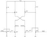
在一个示例中,图6为本申请实施例一提供的偏置电路的另一种结构示意图,所述自偏置电流镜电路包括:第五晶体管Q5、第六晶体管Q6、第七晶体管Q7、第八晶体管Q8、第九晶体管Q9与第四电阻R4;In an example, FIG. 6 is another schematic structural diagram of the bias circuit provided in Embodiment 1 of the present application. The self-bias current mirror circuit includes: a fifth transistor Q5, a sixth transistor Q6, a seventh transistor Q7, an eighth transistor Q8, a ninth transistor Q9 and a fourth resistor R4;
第五晶体管Q5的发射极与第六晶体管Q6的发射极和第九晶体管Q9的发射极连接并且接至电源;第五晶体管Q5的基极与第五晶体管Q5的集电极连接;第五晶体管Q5的集电极与第七晶体管Q7的集电极和使能电路21连接,用于接收所述启动电流;The emitter of the fifth transistor Q5 is connected to the emitter of the sixth transistor Q6 and the emitter of the ninth transistor Q9 and is connected to the power supply; the base of the fifth transistor Q5 is connected to the collector of the fifth transistor Q5; the fifth transistor Q5 The collector of Q7 is connected to the collector of the seventh transistor Q7 and the enabling
第七晶体管Q7的基极与第八晶体管Q8的基极连接,第七晶体管Q7的发射极与第四电阻R4的第一端连接,第四电阻R4的第二端接地;The base of the seventh transistor Q7 is connected to the base of the eighth transistor Q8, the emitter of the seventh transistor Q7 is connected to the first end of the fourth resistor R4, and the second end of the fourth resistor R4 is grounded;
第六晶体管Q6的基极与第五晶体管Q5的基极连接,第六晶体管Q6的集电极与第八晶体管Q8的集电极连接;第八晶体管Q8的基极与第八晶体管Q8的集电极连接,第八晶体管Q8的发射极接地;The base of the sixth transistor Q6 is connected to the base of the fifth transistor Q5, the collector of the sixth transistor Q6 is connected to the collector of the eighth transistor Q8; the base of the eighth transistor Q8 is connected to the collector of the eighth transistor Q8 , the emitter of the eighth transistor Q8 is grounded;
第九晶体管Q9的基极与第五晶体管Q5的基极连接,第九晶体管Q9的集电极与充放电电路连接23,用于输出放电电流。The base of the ninth transistor Q9 is connected to the base of the fifth transistor Q5, and the collector of the ninth transistor Q9 is connected to the charge-
具体的,在偏置电路22中,第六晶体管Q6镜像第五晶体管Q5中的电流,并且由于电阻R4的加入,衰减了环路增益,电路正反馈的增益小于1,使得电路保持稳定。Specifically, in the
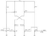
在一个示例中,图7为本申请实施例一提供的充放电电路的结构示意图,充放电电路23包括:电容C1、放电模块和充电模块;其中,所述充电模块包括第十晶体管Q10与第十一晶体管Q11;所述放电模块包括第十二晶体管Q12与第十三晶体管Q13;In an example, FIG. 7 is a schematic structural diagram of the charging and discharging circuit provided in Embodiment 1 of the present application. The charging and discharging
第十晶体管Q10的发射极与第十一晶体管Q11的发射极连接并且接至电源,第十晶体管Q10的基极与第十晶体管Q10的集电极和所述使能电路连接,用于接收充电电流;The emitter of the tenth transistor Q10 is connected to the emitter of the eleventh transistor Q11 and connected to the power supply, and the base of the tenth transistor Q10 is connected to the collector of the tenth transistor Q10 and the enabling circuit for receiving the charging current ;
第十一晶体管Q11的基极与第十晶体管Q10的基极连接,第十一晶体管Q11的集电极与电容C1的第一端连接,电容C1的第二端接地;The base of the eleventh transistor Q11 is connected to the base of the tenth transistor Q10, the collector of the eleventh transistor Q11 is connected to the first end of the capacitor C1, and the second end of the capacitor C1 is grounded;
第十二晶体管Q12的集电极与电容C1的第一端连接,第十二晶体管Q12的发射极接地,第十二晶体管Q12的基极与第十三晶体管Q13的基极连接;第十三晶体管Q13的基极与第十三晶体管Q13的集电极端和所述偏置电路连接,用于接收放电电流;第十三晶体管Q13的发射极接地。The collector of the twelfth transistor Q12 is connected to the first end of the capacitor C1, the emitter of the twelfth transistor Q12 is grounded, and the base of the twelfth transistor Q12 is connected to the base of the thirteenth transistor Q13; The base of Q13 is connected to the collector terminal of the thirteenth transistor Q13 and the bias circuit for receiving the discharge current; the emitter of the thirteenth transistor Q13 is grounded.
当充放电电路23收到充电电流时,第十一晶体管Q11镜像第十晶体管Q10中的电流,镜像生成的电流给电容C1充电;电容C1充电时,放电电流也同时工作,但由于充电电流远大于放电电流,所以电容C1上的电压不受放电电流的影响。当充放电电路收到放电电流时,第十二晶体管Q12镜像第十三晶体管Q13中的放电电流,从而提供电容C1向地的放电路径,实现对电容C1的放电。When the charging and discharging
在一个示例中,图8为本申请实施例一提供的充放电电路的另一种结构示意图,充放电电路23还包括:分压模块以及阶梯镜像支路:In an example, FIG. 8 is another schematic structural diagram of the charging and discharging circuit provided in the first embodiment of the application. The charging and discharging
所述分压模块用于输出阶梯电压,所述阶梯电压与所述阶梯镜像支路之间一一对应;The voltage dividing module is used for outputting a stepped voltage, and the stepped voltage is in one-to-one correspondence with the stepped mirror branch;
所述阶梯镜像支路,连接至对应的阶梯电压,用于根据电容的当前储能和所述阶梯电压之间的关系,启动或停止对所述电容的放电。The ladder mirror branch is connected to the corresponding ladder voltage, and is used for starting or stopping the discharge of the capacitor according to the relationship between the current energy storage of the capacitor and the ladder voltage.
首先图中VREG信号源于充电电流给充放电电路23内置的电容C1充电,使得C1上的电压抬升,然后C1上的电压提供给电平转换电路24,使得电平转换电路24输出VREG,电平转换电路24输出VREG后再作用于充放电电路23的分压模块,使得分压模块工作。First, theVREG signal in the figure comes from the charging current to charge the capacitor C1 built in the charging and discharging
在一个示例中,分压电路输出不同的阶梯电压,不同的阶梯电压对应不同的阶梯镜像电路,阶梯镜像支路用于提供电容C1向地的放电路径。In an example, the voltage divider circuit outputs different staircase voltages, different staircase voltages correspond to different staircase mirror circuits, and the staircase mirror branch is used to provide a discharge path from the capacitor C1 to the ground.
可选的,所述阶梯镜像支路的数量为两个,所述阶梯电压的数量也为两个,不同阶梯镜像支路对应的阶梯电压不同。通过调节阶梯镜像支路的数量,可以实现不同阶段的阶梯放电,从而可以使得所述VREG电压缓慢阶梯下降,使得声音更加悦耳。Optionally, the number of the ladder mirror branches is two, the number of ladder voltages is also two, and the ladder voltages corresponding to different ladder mirror branches are different. By adjusting the number of step mirror branches, different stages of step discharge can be achieved, so that the VREG voltage can be slowly stepped down, making the sound more pleasing to the ear.
在一个示例中,图9为本申请实施例一提供的充放电电路的又一种结构示意图,第一阶梯镜像支路包括:第十四晶体管Q14和第十五晶体管Q15,第二阶梯镜像支路包括:第十六晶体管Q16和第十七晶体管Q17;In an example, FIG. 9 is another schematic structural diagram of the charging and discharging circuit provided in the first embodiment of the application. The first ladder mirror branch includes: a fourteenth transistor Q14 and a fifteenth transistor Q15, and the second ladder mirror branch includes: The circuit includes: a sixteenth transistor Q16 and a seventeenth transistor Q17;
第十四晶体管Q14的基极与第十四晶体管Q14的集电极连接;第十四晶体管Q14的集电极与第十五晶体管Q15的集电极和所述分压电路连接,用于接收对应的阶梯电压;第十四晶体管Q14的发射极与电容C1的第一端连接;The base of the fourteenth transistor Q14 is connected to the collector of the fourteenth transistor Q14; the collector of the fourteenth transistor Q14 is connected to the collector of the fifteenth transistor Q15 and the voltage divider circuit for receiving the corresponding ladder voltage; the emitter of the fourteenth transistor Q14 is connected to the first end of the capacitor C1;
第十五晶体管Q15的基极与第十三晶体管Q13的基极连接,第十五晶体管Q15的发射极接地;The base of the fifteenth transistor Q15 is connected to the base of the thirteenth transistor Q13, and the emitter of the fifteenth transistor Q15 is grounded;
第十四晶体管Q14与第十六晶体管Q16互为镜像,第十五晶体管Q15与第十七晶体管Q17互为镜像。The fourteenth transistor Q14 and the sixteenth transistor Q16 are mirror images of each other, and the fifteenth transistor Q15 and the seventeenth transistor Q17 are mirror images of each other.
结合图示进行举例说明:充放电电路23中存在两个阶梯镜像支路,分别为第一阶梯镜像支路与第二阶梯镜像支路。其中每个阶梯镜像支路都包括两个晶体管,其中,第一阶梯镜像支路包括第十四晶体管Q14和第十五晶体管Q15,第二梯镜像支路包括第十六晶体管Q16和第十七晶体管Q17。其中所述第一阶梯镜像支路中的第十四晶体管Q14与所述第二阶梯镜像支路中的第十六晶体管Q16户为镜像结构,在电路中的连接方式相同。同理,第十五晶体管Q15与第十七晶体管Q17户为镜像结构。An example is given with reference to the drawings: there are two ladder mirror branches in the charging and discharging
在一个示例中,图10为本申请实施例一提供的充放电电路的又一种结构示意图,第十四晶体管Q14的集电极和所述分压电路之间设置有单向导通元件;In an example, FIG. 10 is another schematic structural diagram of the charging and discharging circuit provided in the first embodiment of the application, and a unidirectional conduction element is provided between the collector of the fourteenth transistor Q14 and the voltage divider circuit;
所述单向导通元件的第一端与所述分压电路连接,所述单向导通元件的第二端与第十四晶体管Q14的集电极连接,用于将所述分压电路提供的阶梯电压单向传输至第十四晶体管Q14。The first end of the one-way conduction element is connected to the voltage divider circuit, and the second end of the one-way conduction element is connected to the collector of the fourteenth transistor Q14, for connecting the ladder provided by the voltage divider circuit The voltage is unidirectionally transmitted to the fourteenth transistor Q14.
具体的,所述阶梯镜像支路上存在单向导通元件可以保障电流信号的传输方向只能从分压模块流向第十四晶体管Q14,而不能反向传输,防止信号倒灌。由于所述第一阶梯镜像支路与所述第二阶梯镜像支路户为镜像支路,所以在第十六晶体管Q16与所述分压电路之间亦设置有单向导通元件。Specifically, the presence of a unidirectional conducting element on the step mirror branch can ensure that the transmission direction of the current signal can only flow from the voltage divider module to the fourteenth transistor Q14, but cannot be transmitted in the reverse direction, preventing signal backflow. Since the first ladder mirror branch and the second ladder mirror branch are mirror branches, a unidirectional conduction element is also provided between the sixteenth transistor Q16 and the voltage divider circuit.
在一个示例中,图11为本申请实施例一提供的充放电电路的又一种结构示意图,所述单向导通元件包括:第十八晶体管Q18与第十九晶体管Q19;In an example, FIG. 11 is another schematic structural diagram of the charging and discharging circuit provided in Embodiment 1 of the present application, and the unidirectional conduction element includes: an eighteenth transistor Q18 and a nineteenth transistor Q19;
第十八晶体管Q18的发射极与所述分压电路连接,第十八晶体管Q18的基极与第十八晶体管Q18的集电极连接,第十八晶体管Q18的集电极与第十四晶体管Q14的集电极连接;The emitter of the eighteenth transistor Q18 is connected to the voltage divider circuit, the base of the eighteenth transistor Q18 is connected to the collector of the eighteenth transistor Q18, and the collector of the eighteenth transistor Q18 is connected to the collector of the fourteenth transistor Q14 collector connection;
第十八晶体管Q18与第十九晶体管Q19互为镜像。The eighteenth transistor Q18 and the nineteenth transistor Q19 are mirror images of each other.
具体的,单个阶梯镜像支路中的单向导通元件可以采用晶体管的方式实现。例如,图中第一阶梯镜像支路中的第十八晶体管Q18,作为第一阶梯镜像支路中的单向导通元件;第二阶梯镜像支路中的第十九晶体管Q19,作为第二阶梯镜像支路中的单向导通元件。Specifically, the unidirectional conduction element in a single step mirror branch can be implemented in the form of a transistor. For example, the eighteenth transistor Q18 in the first ladder mirror branch in the figure is used as a unidirectional conducting element in the first ladder mirror branch; the nineteenth transistor Q19 in the second ladder mirror branch is used as the second ladder A unidirectional conducting element in a mirror leg.
在一个示例中,图12为本申请实施例一提供的充放电电路的又一种结构示意图,所述单向导通元件包括:二极管;In an example, FIG. 12 is another schematic structural diagram of the charging and discharging circuit provided in Embodiment 1 of the present application, and the unidirectional conduction element includes: a diode;
所述二极管的正极与所述分压电路连接,所述二极管的负极与第十四晶体管Q14的集电极连接。The anode of the diode is connected to the voltage divider circuit, and the cathode of the diode is connected to the collector of the fourteenth transistor Q14.
具体的,所述阶梯镜像支路上的单向导通元件可以为二极管。例如图12中,第一阶梯镜像支路对应的二极管为D1,所述D1的负极与第十四晶体管Q14的集电极连接。所述第二阶梯镜像支路对应的二极管为D2,所述D2的的负极与第十六晶体管Q16的第一端连接。Specifically, the one-way conducting element on the step mirror branch may be a diode. For example, in FIG. 12 , the diode corresponding to the first step mirror branch is D1, and the cathode of the D1 is connected to the collector of the fourteenth transistor Q14. The diode corresponding to the second step mirror branch is D2, and the cathode of the D2 is connected to the first end of the sixteenth transistor Q16.
在一个示例中,图13为本申请实施例一提供的充放电电路的又一种结构示意图,所述分压模块包括:第二十晶体管Q20、第五电阻R5、第六电阻R6、第七电阻R7以及第八电阻R8;In an example, FIG. 13 is another schematic structural diagram of the charging and discharging circuit provided in Embodiment 1 of the present application. The voltage dividing module includes: a twentieth transistor Q20, a fifth resistor R5, a sixth resistor R6, a seventh resistor Resistor R7 and eighth resistor R8;
第五电阻R5的第一端接接至电源;第五电阻R5的第二端用于输出第一阶梯电压,第五电阻R5的第二端与第六电阻R6的第一端以及所述第一阶梯电压对应的阶梯镜像支路中的第十四晶体管的集电极连接;The first end of the fifth resistor R5 is connected to the power supply; the second end of the fifth resistor R5 is used to output the first step voltage, the second end of the fifth resistor R5 and the first end of the sixth resistor R6 and the The collector of the fourteenth transistor in the step mirror branch corresponding to a step voltage is connected;
第六电阻R6的第二端用于输出第二阶梯电压,第六电阻R6的第二端与第七电阻R7的第一端以及所述第二阶梯电压对应的阶梯镜像支路中的第十四晶体管的集电极连接;The second end of the sixth resistor R6 is used to output the second step voltage, the second end of the sixth resistor R6 and the first end of the seventh resistor R7 and the tenth step in the step mirror branch corresponding to the second step voltage Collector connection of four transistors;
第七电阻R7的第二端与第二十晶体管Q20的集电极连接,第二十晶体管Q20的发射极接地;第八电阻R8的第一端与电平转换电路24连接,用于接收所述供电电压;第八电阻R8的第二端与第二十晶体管Q20的基极连接。The second end of the seventh resistor R7 is connected to the collector of the twentieth transistor Q20, and the emitter of the twentieth transistor Q20 is grounded; the first end of the eighth resistor R8 is connected to the
在充放电电路中,第五电阻R5的第一端接接至电源VCC,第五电阻R5的第二端输出第一阶梯电压,相应的,第一阶梯电压对应的第一阶梯镜像支路与第五电阻R5的第二端连接;类似的,第六电阻R6的第二端输出第二阶梯电压,第二阶梯电压对应的第二阶梯镜像支路与第六电阻R6的第二端连接。In the charging and discharging circuit, the first end of the fifth resistor R5 is connected to the power supply VCC, and the second end of the fifth resistor R5 outputs the first step voltage. Correspondingly, the first step mirror branch corresponding to the first step voltage is the same as The second end of the fifth resistor R5 is connected; similarly, the second end of the sixth resistor R6 outputs a second step voltage, and the second step mirror branch corresponding to the second step voltage is connected to the second end of the sixth resistor R6.
根据图示的情形,可知,在该示例中,第一阶梯电压V1高于第二阶梯电压V2。结合放电场景示例:当电容C1刚开始放电时,电容C1第一端的电压较大,第一阶梯镜像支路的第十四晶体管Q14和第二阶梯镜像支路的第十六晶体管Q16右端处电压(这里的“左/右”仅是参照图示举例,但并未对结构进行限制)高于自身的左端处电压,因此Q14和Q16均导通。相应的,电容C1上的储能经过Q14和Q15构成的第一阶梯镜像支路,以及Q16和Q17构成的第二阶梯镜像支路向地放电。也就是说,这时对电容C1的放电路径包括第十二晶体管Q12所在的路径以及上述两个阶梯镜像支路,三支路径。According to the situation shown in the figure, it can be known that, in this example, the first step voltage V1 is higher than the second step voltage V2. Combined with an example of a discharge scenario: when the capacitor C1 starts to discharge, the voltage at the first end of the capacitor C1 is relatively large, and the right end of the fourteenth transistor Q14 of the first ladder mirror branch and the sixteenth transistor Q16 of the second ladder mirror branch are The voltage ("left/right" here is only an example with reference to the illustration, but does not limit the structure) is higher than the voltage at the left end of itself, so both Q14 and Q16 are turned on. Correspondingly, the stored energy on the capacitor C1 is discharged to the ground through the first ladder mirror branch formed by Q14 and Q15 and the second ladder mirror branch formed by Q16 and Q17. That is to say, the discharge path for the capacitor C1 at this time includes the path where the twelfth transistor Q12 is located, the above-mentioned two ladder mirror branches, and three branch paths.
当电容C1放电一段时间后,电容C1上的电压降低,相应的,第十四晶体管Q14和第十六晶体管Q16右端的电压伴随降低,当电压降低到所述第一阶梯电压与所述第二阶梯电压之间时,第十四晶体管Q14右端处电压低于自身左端处电压,第十六晶体管Q16右端处电压仍高于自身左端处电压。故第十四晶体管Q14断开,但第十六晶体管Q16仍导通。因此,此时的放电路径包括第十二晶体管Q12所在的路径与第二阶梯镜像支路,两支路径。When the capacitor C1 discharges for a period of time, the voltage on the capacitor C1 decreases, and accordingly, the voltages at the right ends of the fourteenth transistor Q14 and the sixteenth transistor Q16 decrease along with it. When the voltage decreases to the first step voltage and the second step voltage When between the step voltages, the voltage at the right end of the fourteenth transistor Q14 is lower than the voltage at the left end thereof, and the voltage at the right end of the sixteenth transistor Q16 is still higher than the voltage at the left end thereof. Therefore, the fourteenth transistor Q14 is turned off, but the sixteenth transistor Q16 is still turned on. Therefore, the discharge path at this time includes the path where the twelfth transistor Q12 is located and the second staircase mirror branch, which are two paths.
后续电容C1继续放电,电容C1上的电压继续降低,当电压降低到低于第二阶梯电压时,第十六晶体管Q16断开,放电路径仅包括第十二晶体管Q12所在的路径,直至电容C1放电结束。The subsequent capacitor C1 continues to discharge, and the voltage on the capacitor C1 continues to decrease. When the voltage drops below the second step voltage, the sixteenth transistor Q16 is turned off, and the discharge path only includes the path where the twelfth transistor Q12 is located, until the capacitor C1 Discharge ends.
本示例中,充放电电路23通过设定分压模块与阶梯镜像支路,达到了对电容C1阶梯放电的效果,使得无源蜂鸣器控制的声音更加平缓悦耳。另外,当C1上的电压放电,使得供电电压VREG小于第二十晶体管Q20的开启电压时,分压电路停止工作,从而降低功耗。In this example, the charge-
在一个示例中,图14为本申请实施例一提供的驱动电路的结构示意图,驱动电路25包括:第二十一晶体管Q21、第二十二晶体管Q22、第二十三晶体管Q23、第二十四晶体管Q24、第二十五晶体管Q25、第二十六晶体管Q26、第九电阻R9、第十电阻R10、第十一电阻R11以及第十二电阻R12;In an example, FIG. 14 is a schematic structural diagram of a driving circuit provided in Embodiment 1 of the present application. The driving
第二十一晶体管Q21的发射极与第九电阻R9的第一端和第二十二晶体管Q22的发射极连接且连至所述供电电压,第二十一晶体管Q21的基极与第九电阻R9的第二端连接;第二十一晶体管Q21的集电极与第二十四晶体管Q24的集电极连接,用于输出所述驱动信号;第二十四晶体管Q24的发射极接地;The emitter of the twenty-first transistor Q21 is connected to the first terminal of the ninth resistor R9 and the emitter of the twenty-second transistor Q22 is connected to the supply voltage, and the base of the twenty-first transistor Q21 is connected to the ninth resistor The second end of R9 is connected; the collector of the twenty-first transistor Q21 is connected to the collector of the twenty-fourth transistor Q24 for outputting the driving signal; the emitter of the twenty-fourth transistor Q24 is grounded;
第二十二晶体管Q22的发射极与第十电阻R10的第一端连接,第二十二晶体管Q22的基极与第十电阻R10的第二端连接;第二十二晶体管Q22的集电极与第二十三晶体管Q23的集电极连接,用于输出所述驱动信号;第二十三晶体管Q23的发射极接地;The emitter of the twenty-second transistor Q22 is connected to the first end of the tenth resistor R10, the base of the twenty-second transistor Q22 is connected to the second end of the tenth resistor R10; the collector of the twenty-second transistor Q22 is connected to the The collector of the twenty-third transistor Q23 is connected to output the driving signal; the emitter of the twenty-third transistor Q23 is grounded;
第十一电阻R11的第一端与二十五晶体管Q25的基极连接,用于接收所述调制控制信号;第十一电阻R11的第二端与第二十三晶体管Q23的基极连接;第二十五晶体管Q25的集电极与第九电阻R9的第二端连接,第二十五晶体管Q25的发射极接地;The first end of the eleventh resistor R11 is connected to the base of the twenty-fifth transistor Q25 for receiving the modulation control signal; the second end of the eleventh resistor R11 is connected to the base of the twenty-third transistor Q23; The collector of the twenty-fifth transistor Q25 is connected to the second end of the ninth resistor R9, and the emitter of the twenty-fifth transistor Q25 is grounded;
第十二电阻R12的第一端与第二十四晶体管Q24的基极连接;第十二电阻R12的第二端与第二十六晶体管Q26的基极连接,用于接收所述调制控制信号的反相信号;第二十六晶体管Q26的集电极与第十电阻R10的第二端连接,第二十六晶体管Q26的发射极接地。The first end of the twelfth resistor R12 is connected to the base of the twenty-fourth transistor Q24; the second end of the twelfth resistor R12 is connected to the base of the twenty-sixth transistor Q26 for receiving the modulation control signal , the collector of the twenty-sixth transistor Q26 is connected to the second end of the tenth resistor R10, and the emitter of the twenty-sixth transistor Q26 is grounded.
电平转换电路24输出的VREG信号,传输到驱动电路25中,作为驱动电路的供电电源。在驱动电路25中,PWM信号为调制控制信号,所述调制控制信号PWM用于给所述扬声器提供频率输入信号。驱动电路25基于调制控制信号,输出驱动信号BUZZ_A和BUZZ_B,用于驱动扬声器。调节所述PWM信号的频率可以使扬声器发出不同的声调。TheVREG signal output by the
在一个示例中,为了提供调制控制信号的反相信号,图15为本申请实施例一提供的驱动电路的另一种结构示意图,驱动电路25还包括:反相器;In an example, in order to provide an inverted signal of the modulation control signal, FIG. 15 is another schematic structural diagram of the driving circuit provided in the first embodiment of the application, and the driving
所述反相器的输入端连至所述调制控制信号,所述反相器的输出端与第二十六晶体管Q26的基极连接。The input terminal of the inverter is connected to the modulation control signal, and the output terminal of the inverter is connected to the base of the twenty-sixth transistor Q26.
本实施例提供的无源蜂鸣器控制集成电路中,所述使能电路用于根据使能信号输出充电电流和启动电流;所述偏置电路基于所述启动电流输出放电电流;所述充放电电路基于所述充电电流和所述放电电流,输出初始电压;所述电平转换电路基于对所述初始电压进行变压处理后,输出供电电压;所述驱动电路基于所述供电电压和调制控制信号,向所述扬声器输出驱动信号,以驱动所述扬声器工作。本申请提供的方案采用集成电路的设计思维,将音乐无源蜂鸣器控制电路达到集成化效果,从而减少了PCB面积,摆脱了分立器件因素的制约。In the passive buzzer control integrated circuit provided in this embodiment, the enabling circuit is configured to output a charging current and a startup current according to an enable signal; the bias circuit outputs a discharging current based on the startup current; the charging current The discharging circuit outputs an initial voltage based on the charging current and the discharging current; the level shifting circuit outputs a supply voltage based on the transformation of the initial voltage; the driving circuit outputs a supply voltage based on the supply voltage and modulation A control signal is used to output a driving signal to the speaker, so as to drive the speaker to work. The solution provided by this application adopts the design thinking of integrated circuits, and achieves the integrated effect of the control circuit of the passive music buzzer, thereby reducing the PCB area and getting rid of the constraints of discrete device factors.
Claims (15)
Priority Applications (1)
| Application Number | Priority Date | Filing Date | Title |
|---|---|---|---|
| CN202210798729.2ACN115188354B (en) | 2022-07-08 | 2022-07-08 | Passive buzzer control IC |
Applications Claiming Priority (1)
| Application Number | Priority Date | Filing Date | Title |
|---|---|---|---|
| CN202210798729.2ACN115188354B (en) | 2022-07-08 | 2022-07-08 | Passive buzzer control IC |
Publications (2)
| Publication Number | Publication Date |
|---|---|
| CN115188354Atrue CN115188354A (en) | 2022-10-14 |
| CN115188354B CN115188354B (en) | 2025-09-30 |
Family
ID=83517935
Family Applications (1)
| Application Number | Title | Priority Date | Filing Date |
|---|---|---|---|
| CN202210798729.2AActiveCN115188354B (en) | 2022-07-08 | 2022-07-08 | Passive buzzer control IC |
Country Status (1)
| Country | Link |
|---|---|
| CN (1) | CN115188354B (en) |
Citations (6)
| Publication number | Priority date | Publication date | Assignee | Title |
|---|---|---|---|---|
| US20120184338A1 (en)* | 2008-09-27 | 2012-07-19 | Kesler Morris P | Integrated repeaters for cell phone applications |
| CN103236843A (en)* | 2013-05-08 | 2013-08-07 | 杭州百事特电子有限公司 | Impulse waveform driver and electromagnetic buzzer |
| CN105790754A (en)* | 2015-11-06 | 2016-07-20 | 成都芯源系统有限公司 | Digital isolation circuit and control method thereof |
| KR20210093828A (en)* | 2012-12-28 | 2021-07-28 | 가부시키가이샤 한도오따이 에네루기 켄큐쇼 | Power storage device control system, power storage system, and electrical appliance |
| CN113812076A (en)* | 2020-03-13 | 2021-12-17 | 电力集成公司 | Mode operation detection for controlling power converter with active clamp switch |
| CN114141220A (en)* | 2021-11-29 | 2022-03-04 | 深圳市太美亚电子科技有限公司 | Drive circuit of music passive buzzer |
- 2022
- 2022-07-08CNCN202210798729.2Apatent/CN115188354B/enactiveActive
Patent Citations (6)
| Publication number | Priority date | Publication date | Assignee | Title |
|---|---|---|---|---|
| US20120184338A1 (en)* | 2008-09-27 | 2012-07-19 | Kesler Morris P | Integrated repeaters for cell phone applications |
| KR20210093828A (en)* | 2012-12-28 | 2021-07-28 | 가부시키가이샤 한도오따이 에네루기 켄큐쇼 | Power storage device control system, power storage system, and electrical appliance |
| CN103236843A (en)* | 2013-05-08 | 2013-08-07 | 杭州百事特电子有限公司 | Impulse waveform driver and electromagnetic buzzer |
| CN105790754A (en)* | 2015-11-06 | 2016-07-20 | 成都芯源系统有限公司 | Digital isolation circuit and control method thereof |
| CN113812076A (en)* | 2020-03-13 | 2021-12-17 | 电力集成公司 | Mode operation detection for controlling power converter with active clamp switch |
| CN114141220A (en)* | 2021-11-29 | 2022-03-04 | 深圳市太美亚电子科技有限公司 | Drive circuit of music passive buzzer |
Also Published As
| Publication number | Publication date |
|---|---|
| CN115188354B (en) | 2025-09-30 |
Similar Documents
| Publication | Publication Date | Title |
|---|---|---|
| CN104917376B (en) | DC/DC converter | |
| JP3251770B2 (en) | Power supply circuit for semiconductor integrated circuit | |
| JP2693874B2 (en) | Delay pulse generation circuit | |
| CN115188354A (en) | Passive Buzzer Control IC | |
| JP2009525921A (en) | Method and circuit for adjusting drive signal frequency of electronic horn with capacitor | |
| CN2884287Y (en) | Circuit for starting current-source or valtage-source | |
| KR20050075427A (en) | Pwm generator | |
| JP3697678B2 (en) | V / F conversion circuit | |
| US5841306A (en) | Pulse generator for generating output pulse of a predetermined width | |
| US20050135125A1 (en) | [charge-pump circuitry] | |
| US5642064A (en) | Voltage to current conversion circuit including a differential amplifier | |
| JPS5846706A (en) | Bridge output stage for electric-acoustic converter audible frequency amplifier | |
| CN219247699U (en) | Three-phase bridge arm drive circuit, three-phase inverter, circuit board and electronic equipment | |
| CN210609093U (en) | Photoelectric oscillation module | |
| US11520366B2 (en) | Voltage generation circuit and associated capacitor charging method and system | |
| JP3916449B2 (en) | Amplifier | |
| JP3067721B2 (en) | Charge pump booster circuit | |
| JPS60128708A (en) | oscillation circuit | |
| JP2812739B2 (en) | Triangular wave generator | |
| JPS5829635Y2 (en) | synchronous oscillation circuit | |
| JPS6116590Y2 (en) | ||
| JPS60245464A (en) | Charge pump type booster circuit | |
| US5834984A (en) | Current controlled oscillator | |
| JPS63169117A (en) | Current pulse generating circuit | |
| JPH0560284B2 (en) |
Legal Events
| Date | Code | Title | Description |
|---|---|---|---|
| PB01 | Publication | ||
| PB01 | Publication | ||
| SE01 | Entry into force of request for substantive examination | ||
| SE01 | Entry into force of request for substantive examination | ||
| GR01 | Patent grant |