CN115148930A - Display panel - Google Patents
Display panelDownload PDFInfo
- Publication number
- CN115148930A CN115148930ACN202210750868.8ACN202210750868ACN115148930ACN 115148930 ACN115148930 ACN 115148930ACN 202210750868 ACN202210750868 ACN 202210750868ACN 115148930 ACN115148930 ACN 115148930A
- Authority
- CN
- China
- Prior art keywords
- layer
- electrodes
- electrode
- display panel
- sub
- Prior art date
- Legal status (The legal status is an assumption and is not a legal conclusion. Google has not performed a legal analysis and makes no representation as to the accuracy of the status listed.)
- Pending
Links
Images


Classifications
- H—ELECTRICITY
- H10—SEMICONDUCTOR DEVICES; ELECTRIC SOLID-STATE DEVICES NOT OTHERWISE PROVIDED FOR
- H10K—ORGANIC ELECTRIC SOLID-STATE DEVICES
- H10K50/00—Organic light-emitting devices
- H10K50/80—Constructional details
- H10K50/805—Electrodes
- H10K50/82—Cathodes
- H10K50/822—Cathodes characterised by their shape
- G—PHYSICS
- G06—COMPUTING OR CALCULATING; COUNTING
- G06F—ELECTRIC DIGITAL DATA PROCESSING
- G06F3/00—Input arrangements for transferring data to be processed into a form capable of being handled by the computer; Output arrangements for transferring data from processing unit to output unit, e.g. interface arrangements
- G06F3/01—Input arrangements or combined input and output arrangements for interaction between user and computer
- G06F3/03—Arrangements for converting the position or the displacement of a member into a coded form
- G06F3/041—Digitisers, e.g. for touch screens or touch pads, characterised by the transducing means
- G06F3/0412—Digitisers structurally integrated in a display
- G—PHYSICS
- G06—COMPUTING OR CALCULATING; COUNTING
- G06F—ELECTRIC DIGITAL DATA PROCESSING
- G06F3/00—Input arrangements for transferring data to be processed into a form capable of being handled by the computer; Output arrangements for transferring data from processing unit to output unit, e.g. interface arrangements
- G06F3/01—Input arrangements or combined input and output arrangements for interaction between user and computer
- G06F3/03—Arrangements for converting the position or the displacement of a member into a coded form
- G06F3/041—Digitisers, e.g. for touch screens or touch pads, characterised by the transducing means
- G06F3/0416—Control or interface arrangements specially adapted for digitisers
- G06F3/04164—Connections between sensors and controllers, e.g. routing lines between electrodes and connection pads
- G—PHYSICS
- G06—COMPUTING OR CALCULATING; COUNTING
- G06F—ELECTRIC DIGITAL DATA PROCESSING
- G06F3/00—Input arrangements for transferring data to be processed into a form capable of being handled by the computer; Output arrangements for transferring data from processing unit to output unit, e.g. interface arrangements
- G06F3/01—Input arrangements or combined input and output arrangements for interaction between user and computer
- G06F3/03—Arrangements for converting the position or the displacement of a member into a coded form
- G06F3/041—Digitisers, e.g. for touch screens or touch pads, characterised by the transducing means
- G06F3/044—Digitisers, e.g. for touch screens or touch pads, characterised by the transducing means by capacitive means
- G06F3/0443—Digitisers, e.g. for touch screens or touch pads, characterised by the transducing means by capacitive means using a single layer of sensing electrodes
- G—PHYSICS
- G06—COMPUTING OR CALCULATING; COUNTING
- G06F—ELECTRIC DIGITAL DATA PROCESSING
- G06F3/00—Input arrangements for transferring data to be processed into a form capable of being handled by the computer; Output arrangements for transferring data from processing unit to output unit, e.g. interface arrangements
- G06F3/01—Input arrangements or combined input and output arrangements for interaction between user and computer
- G06F3/03—Arrangements for converting the position or the displacement of a member into a coded form
- G06F3/041—Digitisers, e.g. for touch screens or touch pads, characterised by the transducing means
- G06F3/044—Digitisers, e.g. for touch screens or touch pads, characterised by the transducing means by capacitive means
- G06F3/0446—Digitisers, e.g. for touch screens or touch pads, characterised by the transducing means by capacitive means using a grid-like structure of electrodes in at least two directions, e.g. using row and column electrodes
- H—ELECTRICITY
- H10—SEMICONDUCTOR DEVICES; ELECTRIC SOLID-STATE DEVICES NOT OTHERWISE PROVIDED FOR
- H10K—ORGANIC ELECTRIC SOLID-STATE DEVICES
- H10K59/00—Integrated devices, or assemblies of multiple devices, comprising at least one organic light-emitting element covered by group H10K50/00
- H10K59/10—OLED displays
- H10K59/12—Active-matrix OLED [AMOLED] displays
- H10K59/122—Pixel-defining structures or layers, e.g. banks
- H—ELECTRICITY
- H10—SEMICONDUCTOR DEVICES; ELECTRIC SOLID-STATE DEVICES NOT OTHERWISE PROVIDED FOR
- H10K—ORGANIC ELECTRIC SOLID-STATE DEVICES
- H10K59/00—Integrated devices, or assemblies of multiple devices, comprising at least one organic light-emitting element covered by group H10K50/00
- H10K59/10—OLED displays
- H10K59/12—Active-matrix OLED [AMOLED] displays
- H10K59/124—Insulating layers formed between TFT elements and OLED elements
- H—ELECTRICITY
- H10—SEMICONDUCTOR DEVICES; ELECTRIC SOLID-STATE DEVICES NOT OTHERWISE PROVIDED FOR
- H10K—ORGANIC ELECTRIC SOLID-STATE DEVICES
- H10K59/00—Integrated devices, or assemblies of multiple devices, comprising at least one organic light-emitting element covered by group H10K50/00
- H10K59/40—OLEDs integrated with touch screens
- H—ELECTRICITY
- H10—SEMICONDUCTOR DEVICES; ELECTRIC SOLID-STATE DEVICES NOT OTHERWISE PROVIDED FOR
- H10K—ORGANIC ELECTRIC SOLID-STATE DEVICES
- H10K59/00—Integrated devices, or assemblies of multiple devices, comprising at least one organic light-emitting element covered by group H10K50/00
- H10K59/80—Constructional details
- H10K59/805—Electrodes
- H10K59/8052—Cathodes
- H10K59/80521—Cathodes characterised by their shape
- G—PHYSICS
- G06—COMPUTING OR CALCULATING; COUNTING
- G06F—ELECTRIC DIGITAL DATA PROCESSING
- G06F2203/00—Indexing scheme relating to G06F3/00 - G06F3/048
- G06F2203/041—Indexing scheme relating to G06F3/041 - G06F3/045
- G06F2203/04107—Shielding in digitiser, i.e. guard or shielding arrangements, mostly for capacitive touchscreens, e.g. driven shields, driven grounds
- G—PHYSICS
- G06—COMPUTING OR CALCULATING; COUNTING
- G06F—ELECTRIC DIGITAL DATA PROCESSING
- G06F2203/00—Indexing scheme relating to G06F3/00 - G06F3/048
- G06F2203/041—Indexing scheme relating to G06F3/041 - G06F3/045
- G06F2203/04111—Cross over in capacitive digitiser, i.e. details of structures for connecting electrodes of the sensing pattern where the connections cross each other, e.g. bridge structures comprising an insulating layer, or vias through substrate
- G—PHYSICS
- G06—COMPUTING OR CALCULATING; COUNTING
- G06F—ELECTRIC DIGITAL DATA PROCESSING
- G06F2203/00—Indexing scheme relating to G06F3/00 - G06F3/048
- G06F2203/041—Indexing scheme relating to G06F3/041 - G06F3/045
- G06F2203/04112—Electrode mesh in capacitive digitiser: electrode for touch sensing is formed of a mesh of very fine, normally metallic, interconnected lines that are almost invisible to see. This provides a quite large but transparent electrode surface, without need for ITO or similar transparent conductive material
Landscapes
- Engineering & Computer Science (AREA)
- General Engineering & Computer Science (AREA)
- Theoretical Computer Science (AREA)
- Physics & Mathematics (AREA)
- Human Computer Interaction (AREA)
- General Physics & Mathematics (AREA)
- Microelectronics & Electronic Packaging (AREA)
- Computer Networks & Wireless Communication (AREA)
- Optics & Photonics (AREA)
- Electroluminescent Light Sources (AREA)
- Devices For Indicating Variable Information By Combining Individual Elements (AREA)
Abstract
Translated fromChinese
Description
Translated fromChinese技术领域technical field
本申请涉及显示技术领域,尤其涉及一种显示面板。The present application relates to the field of display technology, and in particular, to a display panel.
背景技术Background technique
随着便携式电子显示设备的发展,触控技术作为人机互动的界面越来越不可或缺,目前比较常用的触控技术包括外挂式触控技术和内嵌式触控技术。内嵌式触控技术相比外挂式触控技术能够使显示装置更轻薄,因此内嵌式触控技术应于有机发光二极管显示装置(Organic Light-Emitting Diode,OLED)更被关注。With the development of portable electronic display devices, touch technology is becoming more and more indispensable as an interface for human-computer interaction. Currently, commonly used touch technologies include external touch technology and in-cell touch technology. Compared with the external touch technology, the in-cell touch technology can make the display device thinner and lighter, so the in-cell touch technology should be paid more attention to the organic light-emitting diode display device (Organic Light-Emitting Diode, OLED).
现有比较成熟的内嵌式触控技术是在显示面板技术的基础上增加薄膜层和工艺流程,因此会造成结构复杂,增加制程成本。The existing relatively mature in-cell touch technology adds a thin film layer and a process flow on the basis of the display panel technology, so the structure is complicated and the process cost is increased.
发明内容SUMMARY OF THE INVENTION
本申请的目的在于提供一种显示面板,旨在提供简化触控式显示面板的结构和节约成本。The purpose of the present application is to provide a display panel, which aims to simplify the structure of the touch display panel and save the cost.
本申请提供一种显示面板,所述显示面板至少包括:The present application provides a display panel, the display panel includes at least:
阳极层;anode layer;
发光功能层,位于所述阳极层上;a light-emitting functional layer, located on the anode layer;
阴极层,位于所述发光功能层上,且包括多个阴极单元,每个所述阴极单元包括相互绝缘的第一电极和第二电极,在俯视结构中所述第二电极位于所述第一电极的外围。The cathode layer is located on the light-emitting functional layer and includes a plurality of cathode units, each of the cathode units includes a first electrode and a second electrode that are insulated from each other, and the second electrode is located in the first electrode in a plan view the periphery of the electrode.
在一些实施例中,所述显示面板还包括:In some embodiments, the display panel further includes:
阵列基板,所述阵列基板包括源极和漏极;an array substrate, the array substrate includes a source electrode and a drain electrode;
金属层,位于所述阵列基板和所述阳极层之间;a metal layer, located between the array substrate and the anode layer;
其中,所述金属层包括间隔设置的触控驱动信号金属层和连接金属层,所述触控驱动信号金属层与所述第一电极电连接;所述连接金属层连接所述阳极和所述漏极。Wherein, the metal layer includes a touch driving signal metal layer and a connecting metal layer arranged at intervals, and the touch driving signal metal layer is electrically connected to the first electrode; the connecting metal layer connects the anode and the first electrode. drain.
在一些实施例中,多个所述阴极单元呈多行分布,相邻两行所述阴极单元交错设置,且同一行中的所述第二电极相互连接。In some embodiments, a plurality of the cathode units are distributed in multiple rows, the cathode units in two adjacent rows are staggered, and the second electrodes in the same row are connected to each other.
在一些实施例中,多行所述第一电极包括交替设置的连接行电极和虚拟行电极,所述连接行电极包括至少一个第一子电极和多个第二子电极,所述第一子电极与所述触控驱动信号金属层电连接;所述虚拟行电极包括多个所述第二子电极。In some embodiments, a plurality of rows of the first electrodes include alternately arranged connecting row electrodes and dummy row electrodes, the connecting row electrodes include at least one first sub-electrode and a plurality of second sub-electrodes, the first sub-electrodes The electrodes are electrically connected to the touch driving signal metal layer; the dummy row electrodes include a plurality of the second sub-electrodes.
在一些实施例中,所述连接行电极包括多个第一子电极,在一行所述连接行电极中,所述多个第一子电极与所述多个第二子电极交替设置。In some embodiments, the connecting row electrodes include a plurality of first sub-electrodes, and in a row of the connecting row electrodes, the plurality of first sub-electrodes and the plurality of second sub-electrodes are alternately arranged.
在一些实施例中,不同行的所述连接行电极中,所述第一子电极呈列分布,所述触控驱动信号金属层沿所述第一子电极的列方向延伸。In some embodiments, in the connection row electrodes of different rows, the first sub-electrodes are distributed in columns, and the touch driving signal metal layer extends along the column direction of the first sub-electrodes.
在一些实施例中,所述连接行电极中的所述第一子电极与同行的所述第二电极组成触控电极。In some embodiments, the first sub-electrodes in the connecting row electrodes and the second electrodes in the same row form touch electrodes.
在一些实施例中,所述连接行电极中的所述第一子电极与相邻所述虚拟行电极中的所述第二电极组成触控电极。In some embodiments, the first sub-electrodes in the connecting row electrodes and the second electrodes in the adjacent dummy row electrodes form touch electrodes.
在一些实施例中,所述显示面板还包括:In some embodiments, the display panel further includes:
平坦层,位于所述阵列基板与所述阳极层之间,且覆盖所述金属层;a flat layer, located between the array substrate and the anode layer, and covering the metal layer;
像素定义层,位于所述平坦层上,且所述阳极层和所述发光功能层位于所述像素定义层中;a pixel definition layer on the flat layer, and the anode layer and the light-emitting functional layer are located in the pixel definition layer;
公共电极层,位于所述阴极层和所述像素定义层之间;A common electrode layer, located between the cathode layer and the pixel definition layer;
其中,所述平坦层和所述像素定义层在对应所述触控驱动信号金属层的位置分别形成有连通的第一开口和第二开口,所述第一电极在所述第一开口的底部与所述触控驱动信号金属层连接。Wherein, the flat layer and the pixel definition layer are respectively formed with connected first openings and second openings at positions corresponding to the touch driving signal metal layer, and the first electrodes are formed at the bottom of the first openings. connected with the touch driving signal metal layer.
在一些实施例中,所述显示面板还包括:In some embodiments, the display panel further includes:
钝化层,位于所述像素定义层和所述平坦层之间,所述钝化层中形成有连通所述第一开口和所述第二开口的第三开口;a passivation layer, located between the pixel definition layer and the flat layer, and a third opening connecting the first opening and the second opening is formed in the passivation layer;
其中,所述第一开口的所述底部包括暴露于所述第二开口和所述第三开口的第一底部,以及被所述钝化层和所述像素定义层遮挡的第二底部,所述公共电极层覆盖所述第一底部,所述第一电极覆盖所述公共电极层且覆盖所述第二底部。Wherein, the bottom of the first opening includes a first bottom exposed to the second opening and the third opening, and a second bottom blocked by the passivation layer and the pixel definition layer, so The common electrode layer covers the first bottom, and the first electrode covers the common electrode layer and covers the second bottom.
本申请的有益效果是:提供一种显示面板,包括阳极层、发光功能层和阴极层,该发光功能层位于阳极层上,该阴极层位于发光功能层上且包括多个阴极单元。每个阴极单元包括相互绝缘的第一电极和第二电极,其中第二电极位于第一电极的外围。本申请将阴极层分成多个阴极单元,且阴极单元中的第一电极可以作为触控驱动电极,第二电极可以作为触控感应电极,因此相互绝缘的第一电极和第二电极可以形成互容内嵌式的触控电极。由此阴极层不仅作为发光功能层的电极,还可以形成触控电极,即本申请利用阴极层就可以形成触控电极,不需要增加其他膜层,因此可以简化内嵌式触控显示面板的结构,节约成本。The beneficial effect of the present application is to provide a display panel including an anode layer, a light-emitting functional layer and a cathode layer, the light-emitting functional layer is located on the anode layer, and the cathode layer is located on the light-emitting functional layer and includes a plurality of cathode units. Each cathode unit includes a first electrode and a second electrode that are insulated from each other, wherein the second electrode is located at the periphery of the first electrode. In this application, the cathode layer is divided into a plurality of cathode units, and the first electrode in the cathode unit can be used as a touch driving electrode, and the second electrode can be used as a touch sensing electrode, so the mutually insulated first electrode and second electrode can form a mutual Built-in touch electrodes. Therefore, the cathode layer not only serves as the electrode of the light-emitting functional layer, but also can form the touch electrode, that is, the application can form the touch electrode by using the cathode layer without adding other film layers, so the in-cell touch display panel can be simplified. structure to save costs.
附图说明Description of drawings
下面结合附图,通过对本申请的具体实施方式详细描述,将使本申请的技术方案及其它有益效果显而易见。The technical solutions and other beneficial effects of the present application will be apparent through the detailed description of the specific embodiments of the present application in conjunction with the accompanying drawings.
图1是本申请实施例提供的显示面板的结构示意图;FIG. 1 is a schematic structural diagram of a display panel provided by an embodiment of the present application;
图2是本申请实施例提供的阴极层的俯视结构示意图;2 is a schematic top-view structural diagram of a cathode layer provided in an embodiment of the present application;
图3是本申请一种实施例提供的阴极层与触控驱动信号金属层连接的结构示意图;FIG. 3 is a schematic structural diagram of the connection between the cathode layer and the touch driving signal metal layer provided by an embodiment of the present application;
图4是本申请另一种实施例提供的阴极层与触控驱动信号金属层连接的结构示意图。FIG. 4 is a schematic structural diagram of the connection between the cathode layer and the touch driving signal metal layer according to another embodiment of the present application.
具体实施方式Detailed ways
下面将结合本申请实施例中的附图,对本申请实施例中的技术方案进行清楚、完整地描述。显然,所描述的实施例仅仅是本申请一部分实施例,而不是全部的实施例。基于本申请中的实施例,本领域技术人员在没有做出创造性劳动前提下所获得的所有其他实施例,都属于本申请保护的范围。The technical solutions in the embodiments of the present application will be clearly and completely described below with reference to the accompanying drawings in the embodiments of the present application. Obviously, the described embodiments are only a part of the embodiments of the present application, but not all of the embodiments. Based on the embodiments in this application, all other embodiments obtained by those skilled in the art without creative efforts shall fall within the protection scope of this application.
在本申请的描述中,需要理解的是,术语“第一”、“第二”仅用于描述目的,而不能理解为指示或暗示相对重要性或者隐含指明所指示的技术特征的数量。由此,限定有“第一”、“第二”的特征可以明示或者隐含地包括一个或者更多个所述特征。在本申请的描述中,“多个”的含义是两个或两个以上,除非另有明确具体的限定。In the description of the present application, it should be understood that the terms "first" and "second" are only used for description purposes, and cannot be interpreted as indicating or implying relative importance or implicitly indicating the number of indicated technical features. Thus, features defined as "first", "second" may expressly or implicitly include one or more of said features. In the description of the present application, "plurality" means two or more, unless otherwise expressly and specifically defined.
在本申请中,除非另有明确的规定和限定,第一特征在第二特征之“上”或之“下”可以包括第一和第二特征直接接触,也可以包括第一和第二特征不是直接接触而是通过它们之间的另外的特征接触。而且,第一特征在第二特征“之上”、“上方”和“上面”包括第一特征在第二特征正上方和斜上方,或仅仅表示第一特征水平高度高于第二特征。第一特征在第二特征“之下”、“下方”和“下面”包括第一特征在第二特征正下方和斜下方,或仅仅表示第一特征水平高度小于第二特征。In this application, unless otherwise expressly specified and defined, a first feature "on" or "under" a second feature may include direct contact between the first and second features, or may include the first and second features Not directly but through additional features between them. Also, the first feature being "above", "over" and "above" the second feature includes the first feature being directly above and obliquely above the second feature, or simply means that the first feature is level higher than the second feature. The first feature is "below", "below" and "below" the second feature includes the first feature being directly below and diagonally below the second feature, or simply means that the first feature has a lower level than the second feature.
下文的公开提供了许多不同的实施方式或例子用来实现本申请的不同结构。为了简化本申请的公开,下文中对特定例子的部件和设置进行描述。当然,它们仅仅为示例,并且目的不在于限制本申请。此外,本申请可以在不同例子中重复参考数字和/或参考字母,这种重复是为了简化和清楚的目的,其本身不指示所讨论各种实施方式和/或设置之间的关系。此外,本申请提供了的各种特定的工艺和材料的例子,但是本领域普通技术人员可以意识到其他工艺的应用和/或其他材料的使用。The following disclosure provides many different embodiments or examples for implementing different structures of the present application. To simplify the disclosure of the present application, the components and arrangements of specific examples are described below. Of course, they are only examples and are not intended to limit the application. Furthermore, this application may repeat reference numerals and/or reference letters in different instances for the purpose of simplicity and clarity, and does not in itself indicate a relationship between the various embodiments and/or arrangements discussed. In addition, this application provides examples of various specific processes and materials, but one of ordinary skill in the art will recognize the application of other processes and/or the use of other materials.
请参阅图1,图1是本申请实施例提供的显示面板的结构示意图。该显示面板可以应用于内嵌触控式的有机发光二极管显示装置(Organic Light-Emitting Diode,OLED)。请同时参阅图2,图2是本申请实施例提供的阴极层的俯视结构示意图。Please refer to FIG. 1 , which is a schematic structural diagram of a display panel provided by an embodiment of the present application. The display panel can be applied to an in-cell touch-type organic light-emitting diode display device (Organic Light-Emitting Diode, OLED). Please refer to FIG. 2 at the same time. FIG. 2 is a schematic top-view structural diagram of a cathode layer provided by an embodiment of the present application.
该显示面板100至少包括阳极层10、发光功能层11和阴极层12,该发光功能层11位于阳极层10上,该阴极层12位于发光功能层11上且包括多个阴极单元120。其中每个阴极单元120包括相互绝缘的第一电极121和第二电极122,在俯视结构中所述第二电极122位于第一电极121的外围。The
其中,阳极层10的结构包括但不限于氧化ITO/Ag/ITO的叠层结构或者单层的ITO结构。发光功能层11的结构可以包括空穴注入层、空穴传输层、发光层、电子传输层和电子注入层。阴极层12的材料可以为Mg、Ag、和IZO中的一种或多种。Wherein, the structure of the
在一些实施例中,如图1所示,该显示面板100还可以包括阵列基板13和位于阵列基板13和阳极层10之间的金属层14。所述阵列基板13由下至上可以包括基底130、阻挡层131、缓冲层132、有源层133、第一栅绝缘层134a、第一栅极135a、第二栅绝缘层134b、第二栅极135b、层间介质层136、源极137a和漏极137b、第一平坦层138。其中,有源层133位于缓冲层132上,第一栅绝缘层134a位于所述缓冲层132上且覆盖所述有源层133。第一栅极135a位于所述第一栅绝缘层134a上,第二栅绝缘层134b位于所述第一栅绝缘层134a上且覆盖所述第一栅极135a。第二栅极135b位于所述第二栅绝缘层134b上,层间介质层136位于所述第二栅绝缘层134b上且覆盖所述第二栅极135b。源极137a和漏极137b位于所述层间介质层136上,且通过过孔连接在所述有源层133的两侧。第一平坦层138位于所述层间介质层136上,且覆盖所述源极137a和所述漏极137b。In some embodiments, as shown in FIG. 1 , the
基板可以包括刚性基板(如玻璃)和柔性基板(如聚酰亚胺、聚对苯二甲酸乙二醇酯等)其中之一或其组合。阻挡层131可以为聚酰亚胺、环氧树脂等有机绝缘材质,也可以为SiNx、SiOx等无机绝缘材质。缓冲层132可以为由SiOx、SiNx、SiNO中的一种制备而成的单层结构,或者由SiNx/SiOx制备而成的叠层结构。有源层133可以采用铟镓锌氧化物或低温多晶硅制备而成,也可以采用其他任何可以作为有源层的材料制备而成。第一栅绝缘层134a和第二栅绝缘层134b的材料可为SiOx,SiNx,Al2O3/SiNx/SiOx,SiOx/SiNx/SiOx等。第一栅极135a和第二栅极135b的材料可以为Mo或Mo/Al或Mo/Cu或Mo/Cu/IZO或IZO/Cu/IZO或Mo/Cu/ITO或Ni/Cu/Ni或MoTiNi/Cu/MoTiNi或NiCr/Cu/NiCr或CuNb等。层间介质层136可以采用无机材料制备而成,该无机材料为SiOx、SiNx、SiNO中的一种。源极137a和漏极137b的材料可以为Mo或Al/Mo或Mo/Al/Mo或Mo/Cu或Mo/Cu/IZO或IZO/Cu/IZO或Mo/Cu/ITO或Ni/Cu/Ni或MoTiNi/Cu/MoTiNi或NiCr/Cu/NiCr或CuNb等。第一平坦层138所用的材质可以为有机材料。The substrate may include one or a combination of rigid substrates (eg, glass) and flexible substrates (eg, polyimide, polyethylene terephthalate, etc.). The
在一些实施例中,所述金属层14位于所述阵列基板13(或第一平坦层138)上,且包括间隔设置的触控驱动信号金属层141和连接金属层142。该显示面板100还可以包括第二平坦层15,所述第二平坦层15位于所述阵列基板13(或第一平坦层138)上,且覆盖所述金属层14。阳极层10位于所述第二平坦层15上且通过过孔与所述连接金属层142连接,所述连接金属层142通过过孔与所述漏极137b连接,因此连接金属层142可以连接阳极层10与漏极137b。其中,金属层14的材料可以为各种导电性较好的金属或金属氧化物,第二平坦层15所用的材质可以为有机材料。In some embodiments, the
在一些实施例中,阳极层10也可以直接通过过孔与所述漏极137b连接。In some embodiments, the
在一些实施例中,该显示面板100还可以包括像素定义层16,所述阳极层10和所述发光功能层11形成在所述像素定义层16中,图案化的阴极层12位于发光功能层11和像素定义层16上。所述触控驱动信号金属层141与所述阴极层12中的第一电极121电连接,其具体的连接方式可以参见下文。其中,像素定义层16所用的材质可以为有机材料。In some embodiments, the
在一些实施例中,该显示面板100还可以包括位于像素定义层16上的隔垫物17。In some embodiments, the
如图2所示,阴极层12被分成多个阴极单元120,阴极单元120的形成可采用激光刻蚀、湿法刻蚀或精细金属掩模(Fine Metal Mask,FMM)的方式实现。阴极单元120的俯视形状可以为圆形、方形或菱形。多个所述阴极单元120呈多行分布,图中只显示出了6行阴极单元120。多个阴极单元120呈多行分布,说明多个第一电极121呈多行分布,且多个第二电极122对应第一电极121呈多行分布。As shown in FIG. 2 , the
在一些实施例中,相邻两行所述阴极单元120交错设置,例如第二行的阴极单元120向右偏移一定距离,使第二行的阴极单元120位于第一行的两个阴极单元120之间,以节省空间。第三行和第五行的阴极单元120可以与第一行的阴极单元120对齐,第四行和第六行的阴极单元120可以与第二行的阴极单元120对齐。由于第二电极122围绕第一电极121设置,因此多个第一电极121在空间位置上是独立分隔的。同一行中的多个第二电极122可以相互连接。In some embodiments, the
在一些实施例中,多行第一电极121可以包括交替设置的连接行电极12a和虚拟行电极12b,即相邻两行连接行电极12a之间具有一行虚拟行电极12b,或者说相邻两行虚拟行电极12b之间具有一行连接行电极12a。其中,连接行电极12a中的至少一个第一电极121与所述触控驱动信号金属层141电连接,以接收所述触控驱动信号金属层141的触控驱动信号,而作为触控驱动电极。也就是说连接行电极12a中的第一电极121可以全部都与触控驱动信号金属层141电连接,也可以部分与触控驱动信号金属层141电连接。虚拟行电极12b中的第一电极121都不与所述触控驱动信号金属层141电连接。In some embodiments, the plurality of rows of first electrodes 121 may include alternately arranged connecting
在一种实施例中,与触控驱动信号金属层141电连接的第一电极121可以称为第一子电极121a,不与触控驱动信号金属层141电连接的第一电极121可以称为第二子电极121b。当连接行电极12a中的所有第一电极121都通过过孔与触控驱动信号金属层141电连接时,所述连接行电极12a只包括所述第一子电极121a。当连接行电极12a中的部分第一电极121通过过孔与触控驱动信号金属层141电连接时,所述连接行电极12a包括至少一个第一子电极121a和至少一个第二子电极121b,也就是说,一行连接行电极12a中可以有一个第一子电极121a,也可以有多个第一子电极121a。由于虚拟行电极12b中的第一电极121都不与所述触控驱动信号金属层141电连接,所以虚拟行电极12b可以包括多个所述第二子电极121b,即虚拟行电极12b中都是第二子电极121b。In one embodiment, the first electrode 121 electrically connected to the touch driving
如图2所示,当连接行电极12a中包括多个第一子电极121a和多个第二子电极121b时,在一行连接行电极12a中第一子电极121a和第二子电极121b可以交替设置,即第一子电极121a与第二子电极121b相邻设置,或者说相邻的两个第一子电极121a之间具有一个第二子电极121b。As shown in FIG. 2, when the connecting
其中,不同行连接行电极12a中的第一子电极121a可以呈列分布,即在列方向上对齐。可以理解的是,列的方向(列方向)与行的方向(行方向)是垂直的。触控驱动信号金属层141可以沿所述列方向延伸,以将不同行的第一子电极121a连接起来。如图2所示,第一子电极121a可以通过过孔143与下方的触控驱动信号金属层141连接,一个第一子电极121a可以通过四个过孔143来确保与触控驱动信号金属层141的连接。The first sub-electrodes 121a in the
需要说明的是,由于触控驱动信号金属层141位于阴极层12的下方,在俯视图中本看不到所述触控驱动信号金属层141,图2是为了示出触控驱动信号金属层141的位置。It should be noted that since the touch driving
可以理解的是,连接行电极12a和虚拟行电极12b中的第一电极121都可以作为发光功能层11的电极,阳极层10作为发光功能层11的另一电极。当显示面板100处于发光阶段时,第一电极121接受图像信号,与阳极层10形成电场,驱动发光功能层11发光。当显示面板100处于触控阶段时,第一电极121中的第一子电极121a作为触控驱动电极,第二电极122作为触控感应电极,感应电容值的变化,从而确定触控点位。具体的,第二电极122与外围的触控引线连接,所述触控引线与所述第二电极122同层设置,且延伸至非显示区与柔性电路板连接。第一子电极121a接收触控驱动信号,第一子电极121a和第二电极122之间产生耦合电容,手指触摸时耦合电容减少,因此第二电极122接收的电荷量(感测信号)发生变化,并通过触控引线将所述感测信号传递给柔性电路板,所述柔性电路板根据感测信号得到触摸的位置。It can be understood that, the first electrode 121 in the connecting
在一些实施例中,所述连接行电极12a中的第一子电极121a与同行的第二电极122组成触控电极。也就是说第一子电极121a与围绕它的第二电极122组成触控电极,其中第一子电极121a作为触控驱动电极,围绕它的第二电极122作为触控感应电极。In some embodiments, the first sub-electrodes 121a in the connecting
在一些实施例中,所述连接行电极12a中的第一子电极121a与相邻的虚拟行电极12b中的第二电极122组成触控电极。也就是说,第一子电极121a作为触控驱动电极,而与其相邻行的第二电极122作为触控感应电极。In some embodiments, the first sub-electrodes 121a in the connecting
请参阅图3,图3是本申请一种实施例提供的阴极层与触控驱动信号金属层连接的结构示意图。为了便于理解和简要说明,本实施例中与上述实施例中相同的结构使用相同的标号。Please refer to FIG. 3 . FIG. 3 is a schematic structural diagram of the connection between the cathode layer and the touch driving signal metal layer according to an embodiment of the present application. For ease of understanding and brief description, the same reference numerals are used for the same structures in this embodiment as those in the above-mentioned embodiments.
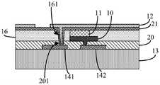
在一些实施例中,显示面板包括阵列基板13、平坦层20和公共电极层21。所述平坦层20位于所述阵列基板13与所述阳极层10之间,且覆盖所述金属层14,所述平坦层20可以是图1实施例中的第二平坦层15。像素定义层16位于所述平坦层20上,且所述阳极层10和所述发光功能层11位于所述像素定义层16中。所述公共电极层21位于所述阴极层12和所述像素定义层16之间。所述平坦层20在对应所述触控驱动信号金属层141的位置形成有第一开口201,所述像素定义层16在对应所述触控驱动信号金属层141的位置形成有第二开口161,第一开口201与第二开口161连通。第一开口201的底部暴露出触控驱动信号金属层141,阴极层12(实际上是第一子电极)在所述第一开口201的底部与所述触控驱动信号金属层141连接。In some embodiments, the display panel includes an
具体的,可以采用激光蚀刻的方式将第一开口201中阴极层12底部的公共电极层21去除掉,则形成的阴极层12中可以在第一开口201的底部与触控驱动信号金属层141搭接。Specifically, the
请参阅图4,图4是本申请另一种实施例提供的阴极层与触控驱动信号金属层连接的结构示意图。为了便于理解和简要说明,本实施例中与上述实施例中相同的结构使用相同的标号。Please refer to FIG. 4 . FIG. 4 is a schematic structural diagram of the connection between the cathode layer and the touch driving signal metal layer according to another embodiment of the present application. For ease of understanding and brief description, the same reference numerals are used for the same structures in this embodiment as those in the above-mentioned embodiments.
在一些实施例中,显示面板还可以包括钝化层22,所述钝化层22位于所述像素定义层16和所述平坦层20之间。所述平坦层20在对应所述触控驱动信号金属层141的位置形成有第一开口202,所述像素定义层16在对应所述触控驱动信号金属层141的位置形成有第二开口161,所述钝化层22中形成有连通所述第一开口202和所述第二开口161的第三开口221,第一开口202的底部2020暴露出触控驱动信号金属层141。钝化层22的材质可以为无机材料。In some embodiments, the display panel may further include a
其中,第一开口202、第二开口161和第三开口221可以形成底切结构U,即所述第一开口202在平行于阵列基板13的横截面的面积,大于第三开口221在平行于阵列基板13的横截面的面积,也大于第二开口161在平行于阵列基板13的横截面的面积。具体的,可以通过干法刻蚀的方式形成所述底切结构U,即像素定义层16和钝化层22刻蚀地少一些,平坦层20刻蚀地相对多一些。所述第一开口202的底部2020包括第一底部2021和第二底部2022,所述第一底部2021暴露于所述第二开口161和所述第三开口221,所述第二底部2022被所述钝化层22和所述像素定义层16遮挡。The first opening 202 , the
在一些实施例中,形成所述底切结构U之后,可以通过调控阴极层12’和公共电极层21’蒸镀的阴影(shadow),使得阴极层12’蒸镀的阴影大于公共电极层21’蒸镀的阴影,进而使得公共电极层21’覆盖所述第一底部2021,阴极层12’覆盖所述公共电极层21’且覆盖所述第二底部2022。因此阴极层12’可以覆盖到第一开口202未被公共电极层21’覆盖的第二底部2022,进而阴极层12’(实际上是第一子电极)在所述第一开口202的底部2020与所述触控驱动信号金属层141连接。In some embodiments, after the undercut structure U is formed, the shadows of the
在本实施例中,公共电极层21’和阴极层12’还形成在所述底切结构U的右侧壁。该显示面板还可以包括封装层(图中未示出),封装层形成在所述阴极层12’上且填充在所述底切结构U中。In this embodiment, the common electrode layer 21' and the cathode layer 12' are also formed on the right side wall of the undercut structure U. The display panel may further include an encapsulation layer (not shown in the figure), the encapsulation layer is formed on the cathode layer 12' and filled in the undercut structure U.
本申请实施例提供的显示面板,包括阳极层10、发光功能层11和阴极层12/12’,该发光功能层11位于阳极层10上,该阴极层12/12’位于发光功能层11上且包括多个阴极单元120。每个阴极单元120包括相互绝缘的第一电极121和第二电极122,其中第二电极122位于第一电极121的外围。本申请将阴极层12/12’分成多个阴极单元120,第一电极121和第二电极122可以形成互容内嵌式的触控电极,不需要增加其他膜层和设备,因此可以简化内嵌式触控显示面板的结构,节约成本。The display panel provided by the embodiment of the present application includes an
本申请实施例还提供一种显示装置,所述显示装置至少包括上述任一种实施例中的显示面板,因此具有与上述任一种显示面板相同的有益效果,在此不再赘述。An embodiment of the present application further provides a display device, the display device includes at least the display panel in any of the above-mentioned embodiments, and thus has the same beneficial effects as any of the above-mentioned display panels, which will not be repeated here.
以上实施例的说明只是用于帮助理解本申请的技术方案及其核心思想;本领域的普通技术人员应当理解:其依然可以对前述各实施例所记载的技术方案进行修改,或者对其中部分技术特征进行等同替换;而这些修改或者替换,并不使相应技术方案的本质脱离本申请各实施例的技术方案的范围。The descriptions of the above embodiments are only used to help understand the technical solutions and core ideas of the present application; those of ordinary skill in the art should understand that the technical solutions recorded in the foregoing embodiments can still be modified, or some of the technical solutions can be modified. The features are equivalently replaced; and these modifications or replacements do not make the essence of the corresponding technical solutions deviate from the scope of the technical solutions of the embodiments of the present application.
Claims (10)
Translated fromChinesePriority Applications (3)
| Application Number | Priority Date | Filing Date | Title |
|---|---|---|---|
| CN202210750868.8ACN115148930A (en) | 2022-06-28 | 2022-06-28 | Display panel |
| US17/759,808US20240188371A1 (en) | 2022-06-28 | 2022-07-13 | Display panel and display device |
| PCT/CN2022/105348WO2024000655A1 (en) | 2022-06-28 | 2022-07-13 | Display panel and display device |
Applications Claiming Priority (1)
| Application Number | Priority Date | Filing Date | Title |
|---|---|---|---|
| CN202210750868.8ACN115148930A (en) | 2022-06-28 | 2022-06-28 | Display panel |
Publications (1)
| Publication Number | Publication Date |
|---|---|
| CN115148930Atrue CN115148930A (en) | 2022-10-04 |
Family
ID=83410524
Family Applications (1)
| Application Number | Title | Priority Date | Filing Date |
|---|---|---|---|
| CN202210750868.8APendingCN115148930A (en) | 2022-06-28 | 2022-06-28 | Display panel |
Country Status (3)
| Country | Link |
|---|---|
| US (1) | US20240188371A1 (en) |
| CN (1) | CN115148930A (en) |
| WO (1) | WO2024000655A1 (en) |
Citations (6)
| Publication number | Priority date | Publication date | Assignee | Title |
|---|---|---|---|---|
| CN104820532A (en)* | 2015-05-08 | 2015-08-05 | 厦门天马微电子有限公司 | Touch device, driving method thereof, and liquid crystal display panel |
| CN106773221A (en)* | 2017-02-17 | 2017-05-31 | 武汉华星光电技术有限公司 | Array base palte and preparation method thereof and In Cell touch-control display panels |
| CN107885400A (en)* | 2017-11-07 | 2018-04-06 | 武汉华星光电半导体显示技术有限公司 | A kind of OLED touch-control display panels and its driving method |
| CN107992225A (en)* | 2017-11-22 | 2018-05-04 | 武汉华星光电半导体显示技术有限公司 | Touch-control display panel and its manufacture method |
| CN110471568A (en)* | 2019-08-15 | 2019-11-19 | 京东方科技集团股份有限公司 | Touch-control structure, touch control display apparatus and preparation method thereof |
| CN114115571A (en)* | 2020-08-26 | 2022-03-01 | 深圳市柔宇科技股份有限公司 | Touch display panel and electronic equipment |
Family Cites Families (8)
| Publication number | Priority date | Publication date | Assignee | Title |
|---|---|---|---|---|
| KR102079251B1 (en)* | 2013-05-21 | 2020-04-08 | 삼성디스플레이 주식회사 | Organic light emitting display apparatus and method for manufacturing the same |
| KR102344331B1 (en)* | 2015-01-15 | 2021-12-28 | 삼성디스플레이 주식회사 | Organic light emitting diode display device |
| CN107394057B (en)* | 2017-07-28 | 2020-04-03 | 武汉天马微电子有限公司 | Organic light emitting display panel and manufacturing method thereof |
| CN111341937A (en)* | 2020-03-13 | 2020-06-26 | 深圳市华星光电半导体显示技术有限公司 | Display panel and preparation method thereof |
| CN111625130B (en)* | 2020-05-15 | 2021-09-24 | 武汉华星光电半导体显示技术有限公司 | Touch display panel and touch display device |
| CN111785742B (en)* | 2020-08-25 | 2022-07-12 | 京东方科技集团股份有限公司 | Display panel, manufacturing method thereof and display device |
| CN114461087B (en)* | 2020-11-09 | 2024-12-17 | 宸鸿科技(厦门)有限公司 | Electronic device with touch control function |
| CN113488514B (en)* | 2021-06-23 | 2022-10-04 | 深圳市华星光电半导体显示技术有限公司 | Display panel and preparation method thereof |
- 2022
- 2022-06-28CNCN202210750868.8Apatent/CN115148930A/enactivePending
- 2022-07-13USUS17/759,808patent/US20240188371A1/enactivePending
- 2022-07-13WOPCT/CN2022/105348patent/WO2024000655A1/ennot_activeCeased
Patent Citations (7)
| Publication number | Priority date | Publication date | Assignee | Title |
|---|---|---|---|---|
| CN104820532A (en)* | 2015-05-08 | 2015-08-05 | 厦门天马微电子有限公司 | Touch device, driving method thereof, and liquid crystal display panel |
| CN106773221A (en)* | 2017-02-17 | 2017-05-31 | 武汉华星光电技术有限公司 | Array base palte and preparation method thereof and In Cell touch-control display panels |
| CN107885400A (en)* | 2017-11-07 | 2018-04-06 | 武汉华星光电半导体显示技术有限公司 | A kind of OLED touch-control display panels and its driving method |
| CN107992225A (en)* | 2017-11-22 | 2018-05-04 | 武汉华星光电半导体显示技术有限公司 | Touch-control display panel and its manufacture method |
| WO2019100478A1 (en)* | 2017-11-22 | 2019-05-31 | 武汉华星光电半导体显示技术有限公司 | Touch display panel and manufacturing method therefor |
| CN110471568A (en)* | 2019-08-15 | 2019-11-19 | 京东方科技集团股份有限公司 | Touch-control structure, touch control display apparatus and preparation method thereof |
| CN114115571A (en)* | 2020-08-26 | 2022-03-01 | 深圳市柔宇科技股份有限公司 | Touch display panel and electronic equipment |
Also Published As
| Publication number | Publication date |
|---|---|
| WO2024000655A1 (en) | 2024-01-04 |
| US20240188371A1 (en) | 2024-06-06 |
Similar Documents
| Publication | Publication Date | Title |
|---|---|---|
| CN212515770U (en) | Touch structure, touch display substrate and touch display device | |
| US20210326001A1 (en) | Display Device Having Touch Sensor | |
| CN106952938B (en) | Flexible display device, manufacturing method thereof and flexible display equipment | |
| US11340745B2 (en) | Touch structure and method for manufacturing the same, touch substrate and touch display device | |
| WO2021227424A1 (en) | Touch-control display panel and touch-control display apparatus | |
| US11921963B2 (en) | Touch structure, touch display structure, and touch display device | |
| CN112860137B (en) | Touch display device | |
| CN114467072B (en) | Touch panel, manufacturing method thereof and display device | |
| CN114127671B (en) | Touch structure and touch display panel | |
| CN108598290A (en) | Flexible display and preparation method thereof | |
| CN117063144A (en) | Touch structure, touch display panel and display device | |
| CN115793882A (en) | Touch display panel and display device | |
| KR102009331B1 (en) | Display device | |
| WO2025180132A1 (en) | Touch display panel and display device | |
| US20240029629A1 (en) | Display panel and mobile terminal | |
| US12189876B2 (en) | Touch panel and preparation method thereof, and display touch apparatus | |
| US20250081828A1 (en) | Display panel and display apparatus | |
| WO2025039534A1 (en) | Display panel and display apparatus | |
| CN115148930A (en) | Display panel | |
| CN218938924U (en) | Touch display panel, display device | |
| CN115715122A (en) | Display panel and display device | |
| WO2023216283A1 (en) | Touch substrate and display panel | |
| CN114335090A (en) | OLED touch display panel and touch display device | |
| TWI767571B (en) | Touch integrated display device | |
| CN115241247A (en) | a display panel |
Legal Events
| Date | Code | Title | Description |
|---|---|---|---|
| PB01 | Publication | ||
| PB01 | Publication | ||
| SE01 | Entry into force of request for substantive examination | ||
| SE01 | Entry into force of request for substantive examination |