CN115136323A - Transistor, electronic device and method for manufacturing transistor - Google Patents
Transistor, electronic device and method for manufacturing transistorDownload PDFInfo
- Publication number
- CN115136323A CN115136323ACN202180014587.XACN202180014587ACN115136323ACN 115136323 ACN115136323 ACN 115136323ACN 202180014587 ACN202180014587 ACN 202180014587ACN 115136323 ACN115136323 ACN 115136323A
- Authority
- CN
- China
- Prior art keywords
- film
- transistor
- gate insulating
- sic
- substrate
- Prior art date
- Legal status (The legal status is an assumption and is not a legal conclusion. Google has not performed a legal analysis and makes no representation as to the accuracy of the status listed.)
- Pending
Links
- 238000000034methodMethods0.000titleclaimsdescription22
- 238000004519manufacturing processMethods0.000titleclaimsdescription8
- 239000004065semiconductorSubstances0.000claimsabstractdescription59
- 239000000758substrateSubstances0.000claimsdescription59
- 239000000463materialSubstances0.000claimsdescription29
- VYPSYNLAJGMNEJ-UHFFFAOYSA-NSilicium dioxideChemical compoundO=[Si]=OVYPSYNLAJGMNEJ-UHFFFAOYSA-N0.000claimsdescription26
- 229910052814silicon oxideInorganic materials0.000claimsdescription26
- 238000000137annealingMethods0.000claimsdescription12
- 238000005268plasma chemical vapour depositionMethods0.000claimsdescription8
- 239000011347resinSubstances0.000claimsdescription2
- 229920005989resinPolymers0.000claimsdescription2
- 239000005001laminate filmSubstances0.000claims1
- 239000010408filmSubstances0.000description303
- 239000010409thin filmSubstances0.000description54
- 239000007789gasSubstances0.000description40
- 230000015572biosynthetic processEffects0.000description21
- 239000002994raw materialSubstances0.000description19
- FFUAGWLWBBFQJT-UHFFFAOYSA-NhexamethyldisilazaneChemical compoundC[Si](C)(C)N[Si](C)(C)CFFUAGWLWBBFQJT-UHFFFAOYSA-N0.000description17
- 238000005229chemical vapour depositionMethods0.000description11
- 238000004544sputter depositionMethods0.000description11
- 238000001678elastic recoil detection analysisMethods0.000description10
- 230000000052comparative effectEffects0.000description9
- -1polyphenylenePolymers0.000description8
- 150000002500ionsChemical class0.000description6
- MYMOFIZGZYHOMD-UHFFFAOYSA-NDioxygenChemical compoundO=OMYMOFIZGZYHOMD-UHFFFAOYSA-N0.000description5
- XLOMVQKBTHCTTD-UHFFFAOYSA-NZinc monoxideChemical compound[Zn]=OXLOMVQKBTHCTTD-UHFFFAOYSA-N0.000description5
- QVGXLLKOCUKJST-UHFFFAOYSA-Natomic oxygenChemical compound[O]QVGXLLKOCUKJST-UHFFFAOYSA-N0.000description5
- 229910001882dioxygenInorganic materials0.000description5
- 238000005259measurementMethods0.000description5
- 239000001301oxygenSubstances0.000description5
- 229910052760oxygenInorganic materials0.000description5
- SLIUAWYAILUBJU-UHFFFAOYSA-NpentaceneChemical compoundC1=CC=CC2=CC3=CC4=CC5=CC=CC=C5C=C4C=C3C=C21SLIUAWYAILUBJU-UHFFFAOYSA-N0.000description5
- 229920000301poly(3-hexylthiophene-2,5-diyl) polymerPolymers0.000description5
- XKRFYHLGVUSROY-UHFFFAOYSA-NArgonChemical compound[Ar]XKRFYHLGVUSROY-UHFFFAOYSA-N0.000description4
- UFHFLCQGNIYNRP-UHFFFAOYSA-NHydrogenChemical compound[H][H]UFHFLCQGNIYNRP-UHFFFAOYSA-N0.000description4
- XUIMIQQOPSSXEZ-UHFFFAOYSA-NSiliconChemical group[Si]XUIMIQQOPSSXEZ-UHFFFAOYSA-N0.000description4
- 239000002178crystalline materialSubstances0.000description4
- 238000010438heat treatmentMethods0.000description4
- 239000012535impuritySubstances0.000description4
- 229910052751metalInorganic materials0.000description4
- 239000002184metalSubstances0.000description4
- 239000000203mixtureSubstances0.000description4
- 125000004430oxygen atomChemical groupO*0.000description4
- 238000000059patterningMethods0.000description4
- 229920001721polyimidePolymers0.000description4
- 239000004642PolyimideSubstances0.000description3
- YXFVVABEGXRONW-UHFFFAOYSA-NTolueneChemical compoundCC1=CC=CC=C1YXFVVABEGXRONW-UHFFFAOYSA-N0.000description3
- 238000004458analytical methodMethods0.000description3
- 239000012159carrier gasSubstances0.000description3
- 239000001257hydrogenSubstances0.000description3
- 229910052739hydrogenInorganic materials0.000description3
- 238000001259photo etchingMethods0.000description3
- 229920003207poly(ethylene-2,6-naphthalate)Polymers0.000description3
- 239000011112polyethylene naphthalateSubstances0.000description3
- 229920000642polymerPolymers0.000description3
- 238000001039wet etchingMethods0.000description3
- ULYOATJQTYIRQV-UHFFFAOYSA-N9,10-bis(octylcarbamoyl)perylene-3,4-dicarboxylic acidChemical compoundC=12C3=CC=C(C(O)=O)C2=C(C(O)=O)C=CC=1C1=CC=C(C(=O)NCCCCCCCC)C2=C1C3=CC=C2C(=O)NCCCCCCCCULYOATJQTYIRQV-UHFFFAOYSA-N0.000description2
- XMWRBQBLMFGWIX-UHFFFAOYSA-NC60 fullereneChemical compoundC12=C3C(C4=C56)=C7C8=C5C5=C9C%10=C6C6=C4C1=C1C4=C6C6=C%10C%10=C9C9=C%11C5=C8C5=C8C7=C3C3=C7C2=C1C1=C2C4=C6C4=C%10C6=C9C9=C%11C5=C5C8=C3C3=C7C1=C1C2=C4C6=C2C9=C5C3=C12XMWRBQBLMFGWIX-UHFFFAOYSA-N0.000description2
- 229910007541Zn OInorganic materials0.000description2
- 229910045601alloyInorganic materials0.000description2
- 239000000956alloySubstances0.000description2
- 229910052786argonInorganic materials0.000description2
- 230000004888barrier functionEffects0.000description2
- 125000004432carbon atomChemical groupC*0.000description2
- 239000002131composite materialSubstances0.000description2
- 150000001875compoundsChemical class0.000description2
- 238000007796conventional methodMethods0.000description2
- 238000009826distributionMethods0.000description2
- 238000005401electroluminescenceMethods0.000description2
- 238000011156evaluationMethods0.000description2
- 229910003472fullereneInorganic materials0.000description2
- 229910052733galliumInorganic materials0.000description2
- 125000004435hydrogen atomChemical group[H]*0.000description2
- 229910052738indiumInorganic materials0.000description2
- PJXISJQVUVHSOJ-UHFFFAOYSA-Nindium(iii) oxideChemical compound[O-2].[O-2].[O-2].[In+3].[In+3]PJXISJQVUVHSOJ-UHFFFAOYSA-N0.000description2
- 239000004973liquid crystal related substanceSubstances0.000description2
- 229910000480nickel oxideInorganic materials0.000description2
- 239000003960organic solventSubstances0.000description2
- 150000003961organosilicon compoundsChemical class0.000description2
- 238000004611spectroscopical analysisMethods0.000description2
- 238000006557surface reactionMethods0.000description2
- 239000012815thermoplastic materialSubstances0.000description2
- 238000001771vacuum depositionMethods0.000description2
- 239000011701zincSubstances0.000description2
- 239000011787zinc oxideSubstances0.000description2
- GYHNNYVSQQEPJS-UHFFFAOYSA-NGalliumChemical compound[Ga]GYHNNYVSQQEPJS-UHFFFAOYSA-N0.000description1
- 229910000990Ni alloyInorganic materials0.000description1
- 229910001096P alloyInorganic materials0.000description1
- OAICVXFJPJFONN-UHFFFAOYSA-NPhosphorusChemical compound[P]OAICVXFJPJFONN-UHFFFAOYSA-N0.000description1
- 239000004952PolyamideSubstances0.000description1
- 239000004698PolyethyleneSubstances0.000description1
- 229920000265PolyparaphenylenePolymers0.000description1
- 239000004793PolystyreneSubstances0.000description1
- 229910004298SiO 2Inorganic materials0.000description1
- 229910006404SnO 2Inorganic materials0.000description1
- GWEVSGVZZGPLCZ-UHFFFAOYSA-NTitan oxideChemical compoundO=[Ti]=OGWEVSGVZZGPLCZ-UHFFFAOYSA-N0.000description1
- 229910052782aluminiumInorganic materials0.000description1
- 125000004429atomChemical group0.000description1
- 238000005452bendingMethods0.000description1
- 230000005540biological transmissionEffects0.000description1
- 229920002678cellulosePolymers0.000description1
- 239000001913celluloseSubstances0.000description1
- 239000000919ceramicSubstances0.000description1
- 238000000576coating methodMethods0.000description1
- 239000004020conductorSubstances0.000description1
- 229910052802copperInorganic materials0.000description1
- 239000010949copperSubstances0.000description1
- XCJYREBRNVKWGJ-UHFFFAOYSA-Ncopper(II) phthalocyanineChemical compound[Cu+2].C12=CC=CC=C2C(N=C2[N-]C(C3=CC=CC=C32)=N2)=NC1=NC([C]1C=CC=CC1=1)=NC=1N=C1[C]3C=CC=CC3=C2[N-]1XCJYREBRNVKWGJ-UHFFFAOYSA-N0.000description1
- 238000010586diagramMethods0.000description1
- 239000000835fiberSubstances0.000description1
- 239000011521glassSubstances0.000description1
- 229910052737goldInorganic materials0.000description1
- 239000010931goldSubstances0.000description1
- RBTKNAXYKSUFRK-UHFFFAOYSA-Nheliogen blueChemical compound[Cu].[N-]1C2=C(C=CC=C3)C3=C1N=C([N-]1)C3=CC=CC=C3C1=NC([N-]1)=C(C=CC=C3)C3=C1N=C([N-]1)C3=CC=CC=C3C1=N2RBTKNAXYKSUFRK-UHFFFAOYSA-N0.000description1
- 150000002431hydrogenChemical class0.000description1
- APFVFJFRJDLVQX-UHFFFAOYSA-Nindium atomChemical compound[In]APFVFJFRJDLVQX-UHFFFAOYSA-N0.000description1
- 229910003437indium oxideInorganic materials0.000description1
- 239000012212insulatorSubstances0.000description1
- 230000001678irradiating effectEffects0.000description1
- 238000010030laminatingMethods0.000description1
- 150000002739metalsChemical class0.000description1
- 229910052750molybdenumInorganic materials0.000description1
- 229910052759nickelInorganic materials0.000description1
- PXHVJJICTQNCMI-UHFFFAOYSA-NnickelSubstances[Ni]PXHVJJICTQNCMI-UHFFFAOYSA-N0.000description1
- 125000004433nitrogen atomChemical groupN*0.000description1
- 230000003287optical effectEffects0.000description1
- GNRSAWUEBMWBQH-UHFFFAOYSA-NoxonickelChemical compound[Ni]=OGNRSAWUEBMWBQH-UHFFFAOYSA-N0.000description1
- 125000002080perylenyl groupChemical groupC1(=CC=C2C=CC=C3C4=CC=CC5=CC=CC(C1=C23)=C45)*0.000description1
- 239000011574phosphorusSubstances0.000description1
- 239000004033plasticSubstances0.000description1
- 229920003023plasticPolymers0.000description1
- 229920000058polyacrylatePolymers0.000description1
- 229920002647polyamidePolymers0.000description1
- 239000004417polycarbonateSubstances0.000description1
- 229920000515polycarbonatePolymers0.000description1
- 229920000728polyesterPolymers0.000description1
- 229920000573polyethylenePolymers0.000description1
- 229920000139polyethylene terephthalatePolymers0.000description1
- 239000005020polyethylene terephthalateSubstances0.000description1
- 229920000098polyolefinPolymers0.000description1
- 229920002223polystyrenePolymers0.000description1
- 229920002635polyurethanePolymers0.000description1
- 239000004814polyurethaneSubstances0.000description1
- 239000004800polyvinyl chlorideSubstances0.000description1
- 229920000915polyvinyl chloridePolymers0.000description1
- YYMBJDOZVAITBP-UHFFFAOYSA-NrubreneChemical compoundC1=CC=CC=C1C(C1=C(C=2C=CC=CC=2)C2=CC=CC=C2C(C=2C=CC=CC=2)=C11)=C(C=CC=C2)C2=C1C1=CC=CC=C1YYMBJDOZVAITBP-UHFFFAOYSA-N0.000description1
- 229910052710siliconInorganic materials0.000description1
- 239000010703siliconSubstances0.000description1
- 238000012358sourcingMethods0.000description1
- 238000005477sputtering targetMethods0.000description1
- VEALVRVVWBQVSL-UHFFFAOYSA-Nstrontium titanateChemical compound[Sr+2].[O-][Ti]([O-])=OVEALVRVVWBQVSL-UHFFFAOYSA-N0.000description1
- 239000000126substanceSubstances0.000description1
- 229920001187thermosetting polymerPolymers0.000description1
- XOLBLPGZBRYERU-UHFFFAOYSA-Ntin dioxideChemical compoundO=[Sn]=OXOLBLPGZBRYERU-UHFFFAOYSA-N0.000description1
- 229910001887tin oxideInorganic materials0.000description1
- 229910052719titaniumInorganic materials0.000description1
- 239000010936titaniumSubstances0.000description1
- FMZQNTNMBORAJM-UHFFFAOYSA-Ntri(propan-2-yl)-[2-[13-[2-tri(propan-2-yl)silylethynyl]pentacen-6-yl]ethynyl]silaneChemical compoundC1=CC=C2C=C3C(C#C[Si](C(C)C)(C(C)C)C(C)C)=C(C=C4C(C=CC=C4)=C4)C4=C(C#C[Si](C(C)C)(C(C)C)C(C)C)C3=CC2=C1FMZQNTNMBORAJM-UHFFFAOYSA-N0.000description1
- GRUMUEUJTSXQOI-UHFFFAOYSA-Nvanadium dioxideChemical compoundO=[V]=OGRUMUEUJTSXQOI-UHFFFAOYSA-N0.000description1
- 239000010457zeoliteSubstances0.000description1
- 229910052725zincInorganic materials0.000description1
Images


Classifications
- H—ELECTRICITY
- H10—SEMICONDUCTOR DEVICES; ELECTRIC SOLID-STATE DEVICES NOT OTHERWISE PROVIDED FOR
- H10D—INORGANIC ELECTRIC SEMICONDUCTOR DEVICES
- H10D30/00—Field-effect transistors [FET]
- H10D30/60—Insulated-gate field-effect transistors [IGFET]
- H10D30/67—Thin-film transistors [TFT]
- H10D30/6729—Thin-film transistors [TFT] characterised by the electrodes
- H10D30/673—Thin-film transistors [TFT] characterised by the electrodes characterised by the shapes, relative sizes or dispositions of the gate electrodes
- H—ELECTRICITY
- H01—ELECTRIC ELEMENTS
- H01L—SEMICONDUCTOR DEVICES NOT COVERED BY CLASS H10
- H01L21/00—Processes or apparatus adapted for the manufacture or treatment of semiconductor or solid state devices or of parts thereof
- H01L21/02—Manufacture or treatment of semiconductor devices or of parts thereof
- H01L21/02104—Forming layers
- H01L21/02107—Forming insulating materials on a substrate
- H01L21/02109—Forming insulating materials on a substrate characterised by the type of layer, e.g. type of material, porous/non-porous, pre-cursors, mixtures or laminates
- H01L21/02112—Forming insulating materials on a substrate characterised by the type of layer, e.g. type of material, porous/non-porous, pre-cursors, mixtures or laminates characterised by the material of the layer
- H01L21/02123—Forming insulating materials on a substrate characterised by the type of layer, e.g. type of material, porous/non-porous, pre-cursors, mixtures or laminates characterised by the material of the layer the material containing silicon
- H01L21/02164—Forming insulating materials on a substrate characterised by the type of layer, e.g. type of material, porous/non-porous, pre-cursors, mixtures or laminates characterised by the material of the layer the material containing silicon the material being a silicon oxide, e.g. SiO2
- C—CHEMISTRY; METALLURGY
- C23—COATING METALLIC MATERIAL; COATING MATERIAL WITH METALLIC MATERIAL; CHEMICAL SURFACE TREATMENT; DIFFUSION TREATMENT OF METALLIC MATERIAL; COATING BY VACUUM EVAPORATION, BY SPUTTERING, BY ION IMPLANTATION OR BY CHEMICAL VAPOUR DEPOSITION, IN GENERAL; INHIBITING CORROSION OF METALLIC MATERIAL OR INCRUSTATION IN GENERAL
- C23C—COATING METALLIC MATERIAL; COATING MATERIAL WITH METALLIC MATERIAL; SURFACE TREATMENT OF METALLIC MATERIAL BY DIFFUSION INTO THE SURFACE, BY CHEMICAL CONVERSION OR SUBSTITUTION; COATING BY VACUUM EVAPORATION, BY SPUTTERING, BY ION IMPLANTATION OR BY CHEMICAL VAPOUR DEPOSITION, IN GENERAL
- C23C16/00—Chemical coating by decomposition of gaseous compounds, without leaving reaction products of surface material in the coating, i.e. chemical vapour deposition [CVD] processes
- C23C16/22—Chemical coating by decomposition of gaseous compounds, without leaving reaction products of surface material in the coating, i.e. chemical vapour deposition [CVD] processes characterised by the deposition of inorganic material, other than metallic material
- C23C16/30—Deposition of compounds, mixtures or solid solutions, e.g. borides, carbides, nitrides
- C23C16/36—Carbonitrides
- C—CHEMISTRY; METALLURGY
- C23—COATING METALLIC MATERIAL; COATING MATERIAL WITH METALLIC MATERIAL; CHEMICAL SURFACE TREATMENT; DIFFUSION TREATMENT OF METALLIC MATERIAL; COATING BY VACUUM EVAPORATION, BY SPUTTERING, BY ION IMPLANTATION OR BY CHEMICAL VAPOUR DEPOSITION, IN GENERAL; INHIBITING CORROSION OF METALLIC MATERIAL OR INCRUSTATION IN GENERAL
- C23C—COATING METALLIC MATERIAL; COATING MATERIAL WITH METALLIC MATERIAL; SURFACE TREATMENT OF METALLIC MATERIAL BY DIFFUSION INTO THE SURFACE, BY CHEMICAL CONVERSION OR SUBSTITUTION; COATING BY VACUUM EVAPORATION, BY SPUTTERING, BY ION IMPLANTATION OR BY CHEMICAL VAPOUR DEPOSITION, IN GENERAL
- C23C16/00—Chemical coating by decomposition of gaseous compounds, without leaving reaction products of surface material in the coating, i.e. chemical vapour deposition [CVD] processes
- C23C16/22—Chemical coating by decomposition of gaseous compounds, without leaving reaction products of surface material in the coating, i.e. chemical vapour deposition [CVD] processes characterised by the deposition of inorganic material, other than metallic material
- C23C16/30—Deposition of compounds, mixtures or solid solutions, e.g. borides, carbides, nitrides
- C23C16/42—Silicides
- C—CHEMISTRY; METALLURGY
- C23—COATING METALLIC MATERIAL; COATING MATERIAL WITH METALLIC MATERIAL; CHEMICAL SURFACE TREATMENT; DIFFUSION TREATMENT OF METALLIC MATERIAL; COATING BY VACUUM EVAPORATION, BY SPUTTERING, BY ION IMPLANTATION OR BY CHEMICAL VAPOUR DEPOSITION, IN GENERAL; INHIBITING CORROSION OF METALLIC MATERIAL OR INCRUSTATION IN GENERAL
- C23C—COATING METALLIC MATERIAL; COATING MATERIAL WITH METALLIC MATERIAL; SURFACE TREATMENT OF METALLIC MATERIAL BY DIFFUSION INTO THE SURFACE, BY CHEMICAL CONVERSION OR SUBSTITUTION; COATING BY VACUUM EVAPORATION, BY SPUTTERING, BY ION IMPLANTATION OR BY CHEMICAL VAPOUR DEPOSITION, IN GENERAL
- C23C16/00—Chemical coating by decomposition of gaseous compounds, without leaving reaction products of surface material in the coating, i.e. chemical vapour deposition [CVD] processes
- C23C16/44—Chemical coating by decomposition of gaseous compounds, without leaving reaction products of surface material in the coating, i.e. chemical vapour deposition [CVD] processes characterised by the method of coating
- C23C16/50—Chemical coating by decomposition of gaseous compounds, without leaving reaction products of surface material in the coating, i.e. chemical vapour deposition [CVD] processes characterised by the method of coating using electric discharges
- H—ELECTRICITY
- H01—ELECTRIC ELEMENTS
- H01L—SEMICONDUCTOR DEVICES NOT COVERED BY CLASS H10
- H01L21/00—Processes or apparatus adapted for the manufacture or treatment of semiconductor or solid state devices or of parts thereof
- H01L21/02—Manufacture or treatment of semiconductor devices or of parts thereof
- H01L21/02104—Forming layers
- H01L21/02107—Forming insulating materials on a substrate
- H01L21/02109—Forming insulating materials on a substrate characterised by the type of layer, e.g. type of material, porous/non-porous, pre-cursors, mixtures or laminates
- H01L21/02112—Forming insulating materials on a substrate characterised by the type of layer, e.g. type of material, porous/non-porous, pre-cursors, mixtures or laminates characterised by the material of the layer
- H01L21/02123—Forming insulating materials on a substrate characterised by the type of layer, e.g. type of material, porous/non-porous, pre-cursors, mixtures or laminates characterised by the material of the layer the material containing silicon
- H01L21/02167—Forming insulating materials on a substrate characterised by the type of layer, e.g. type of material, porous/non-porous, pre-cursors, mixtures or laminates characterised by the material of the layer the material containing silicon the material being a silicon carbide not containing oxygen, e.g. SiC, SiC:H or silicon carbonitrides
- H—ELECTRICITY
- H01—ELECTRIC ELEMENTS
- H01L—SEMICONDUCTOR DEVICES NOT COVERED BY CLASS H10
- H01L21/00—Processes or apparatus adapted for the manufacture or treatment of semiconductor or solid state devices or of parts thereof
- H01L21/02—Manufacture or treatment of semiconductor devices or of parts thereof
- H01L21/02104—Forming layers
- H01L21/02107—Forming insulating materials on a substrate
- H01L21/02109—Forming insulating materials on a substrate characterised by the type of layer, e.g. type of material, porous/non-porous, pre-cursors, mixtures or laminates
- H01L21/022—Forming insulating materials on a substrate characterised by the type of layer, e.g. type of material, porous/non-porous, pre-cursors, mixtures or laminates the layer being a laminate, i.e. composed of sublayers, e.g. stacks of alternating high-k metal oxides
- H—ELECTRICITY
- H01—ELECTRIC ELEMENTS
- H01L—SEMICONDUCTOR DEVICES NOT COVERED BY CLASS H10
- H01L21/00—Processes or apparatus adapted for the manufacture or treatment of semiconductor or solid state devices or of parts thereof
- H01L21/02—Manufacture or treatment of semiconductor devices or of parts thereof
- H01L21/02104—Forming layers
- H01L21/02107—Forming insulating materials on a substrate
- H01L21/02109—Forming insulating materials on a substrate characterised by the type of layer, e.g. type of material, porous/non-porous, pre-cursors, mixtures or laminates
- H01L21/02205—Forming insulating materials on a substrate characterised by the type of layer, e.g. type of material, porous/non-porous, pre-cursors, mixtures or laminates the layer being characterised by the precursor material for deposition
- H01L21/02208—Forming insulating materials on a substrate characterised by the type of layer, e.g. type of material, porous/non-porous, pre-cursors, mixtures or laminates the layer being characterised by the precursor material for deposition the precursor containing a compound comprising Si
- H01L21/02211—Forming insulating materials on a substrate characterised by the type of layer, e.g. type of material, porous/non-porous, pre-cursors, mixtures or laminates the layer being characterised by the precursor material for deposition the precursor containing a compound comprising Si the compound being a silane, e.g. disilane, methylsilane or chlorosilane
- H—ELECTRICITY
- H01—ELECTRIC ELEMENTS
- H01L—SEMICONDUCTOR DEVICES NOT COVERED BY CLASS H10
- H01L21/00—Processes or apparatus adapted for the manufacture or treatment of semiconductor or solid state devices or of parts thereof
- H01L21/02—Manufacture or treatment of semiconductor devices or of parts thereof
- H01L21/02104—Forming layers
- H01L21/02107—Forming insulating materials on a substrate
- H01L21/02225—Forming insulating materials on a substrate characterised by the process for the formation of the insulating layer
- H01L21/0226—Forming insulating materials on a substrate characterised by the process for the formation of the insulating layer formation by a deposition process
- H01L21/02263—Forming insulating materials on a substrate characterised by the process for the formation of the insulating layer formation by a deposition process deposition from the gas or vapour phase
- H01L21/02271—Forming insulating materials on a substrate characterised by the process for the formation of the insulating layer formation by a deposition process deposition from the gas or vapour phase deposition by decomposition or reaction of gaseous or vapour phase compounds, i.e. chemical vapour deposition
- H01L21/02274—Forming insulating materials on a substrate characterised by the process for the formation of the insulating layer formation by a deposition process deposition from the gas or vapour phase deposition by decomposition or reaction of gaseous or vapour phase compounds, i.e. chemical vapour deposition in the presence of a plasma [PECVD]
- H—ELECTRICITY
- H01—ELECTRIC ELEMENTS
- H01L—SEMICONDUCTOR DEVICES NOT COVERED BY CLASS H10
- H01L21/00—Processes or apparatus adapted for the manufacture or treatment of semiconductor or solid state devices or of parts thereof
- H01L21/02—Manufacture or treatment of semiconductor devices or of parts thereof
- H01L21/02104—Forming layers
- H01L21/02107—Forming insulating materials on a substrate
- H01L21/02296—Forming insulating materials on a substrate characterised by the treatment performed before or after the formation of the layer
- H01L21/02299—Forming insulating materials on a substrate characterised by the treatment performed before or after the formation of the layer pre-treatment
- H01L21/02304—Forming insulating materials on a substrate characterised by the treatment performed before or after the formation of the layer pre-treatment formation of intermediate layers, e.g. buffer layers, layers to improve adhesion, lattice match or diffusion barriers
- H—ELECTRICITY
- H01—ELECTRIC ELEMENTS
- H01L—SEMICONDUCTOR DEVICES NOT COVERED BY CLASS H10
- H01L21/00—Processes or apparatus adapted for the manufacture or treatment of semiconductor or solid state devices or of parts thereof
- H01L21/02—Manufacture or treatment of semiconductor devices or of parts thereof
- H01L21/02104—Forming layers
- H01L21/02107—Forming insulating materials on a substrate
- H01L21/02296—Forming insulating materials on a substrate characterised by the treatment performed before or after the formation of the layer
- H01L21/02318—Forming insulating materials on a substrate characterised by the treatment performed before or after the formation of the layer post-treatment
- H—ELECTRICITY
- H01—ELECTRIC ELEMENTS
- H01L—SEMICONDUCTOR DEVICES NOT COVERED BY CLASS H10
- H01L21/00—Processes or apparatus adapted for the manufacture or treatment of semiconductor or solid state devices or of parts thereof
- H01L21/02—Manufacture or treatment of semiconductor devices or of parts thereof
- H01L21/04—Manufacture or treatment of semiconductor devices or of parts thereof the devices having potential barriers, e.g. a PN junction, depletion layer or carrier concentration layer
- H01L21/18—Manufacture or treatment of semiconductor devices or of parts thereof the devices having potential barriers, e.g. a PN junction, depletion layer or carrier concentration layer the devices having semiconductor bodies comprising elements of Group IV of the Periodic Table or AIIIBV compounds with or without impurities, e.g. doping materials
- H01L21/30—Treatment of semiconductor bodies using processes or apparatus not provided for in groups H01L21/20 - H01L21/26
- H01L21/31—Treatment of semiconductor bodies using processes or apparatus not provided for in groups H01L21/20 - H01L21/26 to form insulating layers thereon, e.g. for masking or by using photolithographic techniques; After treatment of these layers; Selection of materials for these layers
- H—ELECTRICITY
- H01—ELECTRIC ELEMENTS
- H01L—SEMICONDUCTOR DEVICES NOT COVERED BY CLASS H10
- H01L21/00—Processes or apparatus adapted for the manufacture or treatment of semiconductor or solid state devices or of parts thereof
- H01L21/02—Manufacture or treatment of semiconductor devices or of parts thereof
- H01L21/04—Manufacture or treatment of semiconductor devices or of parts thereof the devices having potential barriers, e.g. a PN junction, depletion layer or carrier concentration layer
- H01L21/34—Manufacture or treatment of semiconductor devices or of parts thereof the devices having potential barriers, e.g. a PN junction, depletion layer or carrier concentration layer the devices having semiconductor bodies not provided for in groups H01L21/18, H10D48/04 and H10D48/07, with or without impurities, e.g. doping materials
- H01L21/44—Manufacture of electrodes on semiconductor bodies using processes or apparatus not provided for in groups H01L21/38 - H01L21/428
- H01L21/441—Deposition of conductive or insulating materials for electrodes
- H—ELECTRICITY
- H10—SEMICONDUCTOR DEVICES; ELECTRIC SOLID-STATE DEVICES NOT OTHERWISE PROVIDED FOR
- H10D—INORGANIC ELECTRIC SEMICONDUCTOR DEVICES
- H10D30/00—Field-effect transistors [FET]
- H10D30/01—Manufacture or treatment
- H10D30/021—Manufacture or treatment of FETs having insulated gates [IGFET]
- H10D30/031—Manufacture or treatment of FETs having insulated gates [IGFET] of thin-film transistors [TFT]
- H—ELECTRICITY
- H10—SEMICONDUCTOR DEVICES; ELECTRIC SOLID-STATE DEVICES NOT OTHERWISE PROVIDED FOR
- H10D—INORGANIC ELECTRIC SEMICONDUCTOR DEVICES
- H10D30/00—Field-effect transistors [FET]
- H10D30/60—Insulated-gate field-effect transistors [IGFET]
- H10D30/67—Thin-film transistors [TFT]
- H10D30/6729—Thin-film transistors [TFT] characterised by the electrodes
- H10D30/6737—Thin-film transistors [TFT] characterised by the electrodes characterised by the electrode materials
- H10D30/6739—Conductor-insulator-semiconductor electrodes
- H—ELECTRICITY
- H10—SEMICONDUCTOR DEVICES; ELECTRIC SOLID-STATE DEVICES NOT OTHERWISE PROVIDED FOR
- H10D—INORGANIC ELECTRIC SEMICONDUCTOR DEVICES
- H10D30/00—Field-effect transistors [FET]
- H10D30/60—Insulated-gate field-effect transistors [IGFET]
- H10D30/67—Thin-film transistors [TFT]
- H10D30/674—Thin-film transistors [TFT] characterised by the active materials
- H10D30/6755—Oxide semiconductors, e.g. zinc oxide, copper aluminium oxide or cadmium stannate
- H—ELECTRICITY
- H10—SEMICONDUCTOR DEVICES; ELECTRIC SOLID-STATE DEVICES NOT OTHERWISE PROVIDED FOR
- H10D—INORGANIC ELECTRIC SEMICONDUCTOR DEVICES
- H10D99/00—Subject matter not provided for in other groups of this subclass
- H—ELECTRICITY
- H10—SEMICONDUCTOR DEVICES; ELECTRIC SOLID-STATE DEVICES NOT OTHERWISE PROVIDED FOR
- H10K—ORGANIC ELECTRIC SOLID-STATE DEVICES
- H10K10/00—Organic devices specially adapted for rectifying, amplifying, oscillating or switching; Organic capacitors or resistors having potential barriers
- H10K10/40—Organic transistors
- H10K10/46—Field-effect transistors, e.g. organic thin-film transistors [OTFT]
- H10K10/462—Insulated gate field-effect transistors [IGFETs]
- H10K10/468—Insulated gate field-effect transistors [IGFETs] characterised by the gate dielectrics
- H10K10/474—Insulated gate field-effect transistors [IGFETs] characterised by the gate dielectrics the gate dielectric comprising a multilayered structure
- H—ELECTRICITY
- H01—ELECTRIC ELEMENTS
- H01L—SEMICONDUCTOR DEVICES NOT COVERED BY CLASS H10
- H01L21/00—Processes or apparatus adapted for the manufacture or treatment of semiconductor or solid state devices or of parts thereof
- H01L21/02—Manufacture or treatment of semiconductor devices or of parts thereof
- H01L21/02104—Forming layers
- H01L21/02365—Forming inorganic semiconducting materials on a substrate
- H01L21/02518—Deposited layers
- H01L21/02521—Materials
- H01L21/02551—Group 12/16 materials
- H01L21/02554—Oxides
- H—ELECTRICITY
- H01—ELECTRIC ELEMENTS
- H01L—SEMICONDUCTOR DEVICES NOT COVERED BY CLASS H10
- H01L21/00—Processes or apparatus adapted for the manufacture or treatment of semiconductor or solid state devices or of parts thereof
- H01L21/02—Manufacture or treatment of semiconductor devices or of parts thereof
- H01L21/02104—Forming layers
- H01L21/02365—Forming inorganic semiconducting materials on a substrate
- H01L21/02518—Deposited layers
- H01L21/02521—Materials
- H01L21/02565—Oxide semiconducting materials not being Group 12/16 materials, e.g. ternary compounds
- H—ELECTRICITY
- H01—ELECTRIC ELEMENTS
- H01L—SEMICONDUCTOR DEVICES NOT COVERED BY CLASS H10
- H01L21/00—Processes or apparatus adapted for the manufacture or treatment of semiconductor or solid state devices or of parts thereof
- H01L21/02—Manufacture or treatment of semiconductor devices or of parts thereof
- H01L21/02104—Forming layers
- H01L21/02365—Forming inorganic semiconducting materials on a substrate
- H01L21/02612—Formation types
- H01L21/02617—Deposition types
- H01L21/02631—Physical deposition at reduced pressure, e.g. MBE, sputtering, evaporation
Landscapes
- Engineering & Computer Science (AREA)
- Physics & Mathematics (AREA)
- Chemical & Material Sciences (AREA)
- Microelectronics & Electronic Packaging (AREA)
- Power Engineering (AREA)
- Condensed Matter Physics & Semiconductors (AREA)
- General Physics & Mathematics (AREA)
- Manufacturing & Machinery (AREA)
- Computer Hardware Design (AREA)
- Chemical Kinetics & Catalysis (AREA)
- Plasma & Fusion (AREA)
- General Chemical & Material Sciences (AREA)
- Materials Engineering (AREA)
- Mechanical Engineering (AREA)
- Metallurgy (AREA)
- Organic Chemistry (AREA)
- Inorganic Chemistry (AREA)
- Thin Film Transistor (AREA)
Abstract
Description
Translated fromChinese技术领域technical field
本发明系关于晶体管、电子装置及晶体管之制造方法。The present invention relates to a transistor, an electronic device and a method for manufacturing the transistor.
本申请案主张基于2020年2月20日于日本申请之特愿2020-027134之优先权,将其内容引用于本文。This application claims priority based on Japanese Patent Application No. 2020-027134 filed in Japan on February 20, 2020, the contents of which are incorporated herein by reference.
背景技术Background technique
薄膜晶体管(Thin Film Transistor,TFT)广泛用于液晶显示设备及有机电激发光(Electro Luminescence:EL)显示设备等中。Thin film transistors (Thin Film Transistor, TFT) are widely used in liquid crystal display devices, organic electroluminescence (Electro Luminescence: EL) display devices, and the like.
作为薄膜晶体管之半导体膜材料,氧化物半导体受到关注。其中,使用In-Ga-Zn-O(IGZO(氧化铟镓锌))等非晶质氧化物半导体之薄膜晶体管受到关注。As a semiconductor film material for thin film transistors, oxide semiconductors have attracted attention. Among them, a thin film transistor using an amorphous oxide semiconductor such as In-Ga-Zn-O (IGZO (Indium Gallium Zinc Oxide)) is attracting attention.
又,薄膜晶体管之闸极绝缘层例如专利文献1所记载,藉由CVD(Chemical VaporDeposition(化学气相沉积))法成膜。近年来,要求显示设备进一步高性能化,从而寻求一种高绝缘性能、高可靠性之薄膜晶体管。In addition, the gate insulating layer of the thin film transistor is, for example, described in
[先前技术文献][Prior Art Literature]
[专利文献][Patent Literature]
[专利文献1]日本特开2017-107952号公报[Patent Document 1] Japanese Patent Laid-Open No. 2017-107952
发明内容SUMMARY OF THE INVENTION
本发明之一态样系一种晶体管,其具有闸极电极、闸极绝缘膜、半导体膜、源极电极及汲极电极之薄膜晶体管,且上述闸极绝缘膜系交替积层SiOx膜与SiCyNz膜而成之积层膜,构成上述积层膜之膜之总数为3层以上18层以下,构成上述积层膜之各膜之膜厚为25nm以上150nm以下。One aspect of the present invention is a transistor comprising a thin film transistor including a gate electrode, a gate insulating film, a semiconductor film, a source electrode and a drain electrode, wherein the gate insulating film is alternately laminated with aSiOx film and In the laminated film formed of the SiCy Nz film, the total number of films constituting the laminated film is 3 to 18 layers, and the thickness of each film constituting the laminated film is 25 nm to 150 nm.
附图说明Description of drawings
图1系本实施形态之薄膜晶体管之一例之剖面的示意图。FIG. 1 is a schematic diagram of a cross section of an example of the thin film transistor of the present embodiment.
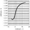
图2系表示实施例1中制造之薄膜晶体管之晶体管特性之图。FIG. 2 is a graph showing transistor characteristics of the thin film transistor fabricated in Example 1. FIG.
图3系表示实施例2中制造之薄膜晶体管之晶体管特性之图。FIG. 3 is a graph showing transistor characteristics of the thin film transistor fabricated in Example 2. FIG.
图4系表示实施例3中制造之薄膜晶体管之晶体管特性之图。FIG. 4 is a graph showing transistor characteristics of the thin film transistor fabricated in Example 3. FIG.
图5系表示实施例4中制造之薄膜晶体管之晶体管特性之图。FIG. 5 is a graph showing transistor characteristics of the thin film transistor fabricated in Example 4. FIG.
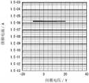
图6系表示比较例1中制造之薄膜晶体管之晶体管特性之图。FIG. 6 is a graph showing transistor characteristics of the thin film transistor produced in Comparative Example 1. FIG.
图7系表示比较例2中制造之薄膜晶体管之晶体管特性之图。FIG. 7 is a graph showing transistor characteristics of the thin film transistor manufactured in Comparative Example 2. FIG.
具体实施方式Detailed ways
<薄膜晶体管><Thin Film Transistor>
本实施形态系具有闸极电极、闸极绝缘膜、半导体膜、源极电极及汲极电极之薄膜晶体管。This embodiment is a thin film transistor having a gate electrode, a gate insulating film, a semiconductor film, a source electrode, and a drain electrode.
于本实施形态中,闸极绝缘膜系交替积层SiOx膜与SiCyNz膜而成之积层膜。In this embodiment, the gate insulating film is a laminated film formed by alternately laminating aSiOx film and a SiCy Nz film.
图1所示之薄膜晶体管1系形成于基板11之表面之底闸极型薄膜晶体管。薄膜晶体管1具备闸极电极12、闸极绝缘膜13、半导体膜14、源极电极15a及汲极电极15b。The
以下对各构成进行说明。Each configuration will be described below.
《基板》"Substrate"
基板11之材料可例举:金属、结晶质材料、非晶质材料、导体、半导体、绝缘体、纤维、玻璃、陶瓷、沸石、塑料、热硬化性及热塑性材料。又,基板11亦可为光学组件、涂装基板、膜等。Examples of the material of the
作为结晶性材料,可例举:单晶质材料、多晶质材料或部分晶质材料。As a crystalline material, a single crystalline material, a polycrystalline material, or a partially crystalline material can be mentioned.
作为热塑性材料,可例举:聚丙烯酸酯、聚碳酸酯、聚胺基甲酸酯、聚苯乙烯、纤维素聚合物、聚烯烃、聚酰胺、聚酰亚胺、聚酯、聚苯、聚乙烯、聚对苯二甲酸乙二酯、聚萘二甲酸乙二酯、聚丙烯、乙烯-乙烯基共聚物(ethylene-vinyl copolymer)、聚氯乙烯等。该等材料亦可经掺杂。As the thermoplastic material, polyacrylate, polycarbonate, polyurethane, polystyrene, cellulose polymer, polyolefin, polyamide, polyimide, polyester, polyphenylene, poly Ethylene, polyethylene terephthalate, polyethylene naphthalate, polypropylene, ethylene-vinyl copolymer, polyvinyl chloride, and the like. These materials can also be doped.
于本实施形态中,作为基板11之材质,较佳为聚酰亚胺或聚萘二甲酸乙二酯。In this embodiment, as the material of the
聚酰亚胺之软化点为290℃。聚萘二甲酸乙二酯之软化点为120℃。The softening point of the polyimide is 290°C. The softening point of polyethylene naphthalate is 120°C.
于本实施形态中,基板11较佳为具有可挠性之基板。此处,可挠性系指即便对基板11施加自重程度之力亦不剪断或断裂,而可使基板11弯曲之性质。In this embodiment, the
又,因自重程度之力而弯曲之性质亦属于可挠性。于本实施形态中,基板11之可挠性根据基板11之材质、大小、厚度、或温度等环境等等发生变化。In addition, the property of bending due to the force of its own weight is also flexible. In this embodiment, the flexibility of the
作为具有可挠性之基板11,较佳为由树脂材料构成之基板。As the
再者,作为基板11,可使用1片长条状之基板。又,于本实施形态中,关于基板11,亦可设为将复数个单位基板连接而形成为长条状之构成。In addition, as the
《闸极电极》"Gate Electrode"
闸极电极12形成于基板11之表面。闸极电极12具有导电性。作为构成闸极电极12之材料,并无特别限定。于本实施形态中,可例举:Al、Mo、Cu、Ti、Au、Ni等。The
闸极电极12可为单独使用该等材料之积层体,亦可为并用2种以上该等材料之积层体。The
又,亦可使用包含该等材料之合金。作为闸极电极12中使用之合金,可例举镍与磷之合金。Moreover, alloys containing these materials can also be used. As the alloy used for the
作为闸极电极12之形状,并无特别限定,就通道长度及通道宽度之控制性之观点而言,较佳为将薄膜晶体管之通道长度方向及通道宽度方向作为长宽之俯视方形。The shape of the
作为闸极电极12之大小,只要为可确保薄膜晶体管之通道长度及通道宽度之大小即可。The size of the
此处,薄膜晶体管之通道长度方向系指薄膜晶体管之源极电极15a及汲极电极15b之对向方向。Here, the channel length direction of the thin film transistor refers to the opposite direction of the
又,该薄膜晶体管之通道宽度方向系指与薄膜晶体管之通道长度方向正交且与基板11之表面平行之方向。In addition, the channel width direction of the thin film transistor refers to a direction orthogonal to the channel length direction of the thin film transistor and parallel to the surface of the
闸极电极12之平均厚度可例举50nm以上500nm以下、100nm以上400nm以下。The average thickness of the
再者,为了使闸极绝缘膜13之覆盖性变得良好,闸极电极12之厚度方向之剖面可设为朝基板11扩张之锥形。作为使闸极电极12成为锥形之情形时之倾斜角度,较佳为30°以上40°以下。Furthermore, in order to improve the coverage of the
《闸极绝缘膜》"Gate Insulating Film"
闸极绝缘膜13以覆盖闸极电极12之方式形成于基板11之一面。于本实施形态中,将基板11中之设置有闸极电极12之面设为上主面。于本实施形态中,闸极绝缘膜13系交替形成SiOx膜与SiCyNz膜而成之积层膜。The
SiOx膜之x较佳为1.7以上2.4以下,更佳为1.9以上2.1以下。The x of the SiOx film is preferably 1.7 or more and 2.4 or less, more preferably 1.9 or more and 2.1 or less.
SiCyNz膜之y较佳为1.0以上3.5以下,更佳为1.0以上2.0以下。SiCyNz膜之z较佳为超过0且为1.0以下,更佳为0.2以上0.7以下。The y of the SiCy Nz film is preferably 1.0 or more and 3.5 or less, more preferably 1.0 or more and 2.0 or less. The z of the SiCy Nz film is preferably more than 0 and 1.0 or less, more preferably 0.2 or more and 0.7 or less.
构成积层膜之膜之总数为3层以上18层以下,较佳为4层以上16层以下。于本实施形态中,构成积层膜之膜之总数可为奇数,亦可为偶数,但偶数更佳。The total number of films constituting the laminated film is 3 or more and 18 or less, preferably 4 or more and 16 or less. In this embodiment, the total number of films constituting the laminated film may be an odd number or an even number, but an even number is more preferable.
于构成积层膜之膜之总数为奇数之情形时,较佳为以与半导体膜14相接之层成为SiOx膜之方式形成。即,较佳为自基板11之侧依序具备SiOx膜、SiCyNz膜、SiOx膜。When the total number of films constituting the laminated film is an odd number, it is preferable to form the layer in contact with the
积层膜较佳为于闸极电极12之上依序交替形成SiCyNz膜、SiOx膜。又,较佳为以与半导体膜14相接之层成为SiOx膜之方式形成。The laminated film is preferably formed by alternately forming a SiCy Nz film and a SiOx film on the
即,于底闸极型之情形时,积层膜较佳为以半导体膜14侧之最上层成为SiOx膜之方式形成。That is, in the case of the bottom gate type, the build-up film is preferably formed so that the uppermost layer on the side of the
于顶闸极型之情形时,较佳为以半导体膜14侧之最下层成为SiOx膜之方式形成。In the case of the top gate type, it is preferable to form the lowermost layer on the side of the
SiOx膜对于水分(H2O)或氢(H2)之类的对薄膜晶体管特性造成影响之杂质,具有阻隔性。而且,于本实施形态中,藉由制成上述层构成之积层膜,而SiOx膜之界面增加。该等杂质被截留于各界面中。因此,阻隔性提升,杂质变得不易扩散至半导体膜。其结果为,可实现可靠性较高之装置。又,藉由使积层膜具有SiCyNz膜,可制成被赋予挠性从而对应力之耐性亦得到提升之装置。The SiOx film has barrier properties against impurities such as moisture (H2 O) or hydrogen (H2 ) that affect the characteristics of thin film transistors. Furthermore, in the present embodiment, the interface of the SiOx film is increased by forming a laminated film having the above-mentioned layer structure. These impurities are trapped in the interfaces. Therefore, the barrier property is improved, and it becomes difficult for impurities to diffuse into the semiconductor film. As a result, a device with high reliability can be realized. In addition, by providing the laminated film with a SiCy Nz film, a device in which flexibility is imparted and resistance to stress is also improved can be obtained.
作为藉由电浆CVD装置成膜SiO2系薄膜之习知方法,就提高闸极绝缘膜之绝缘性之观点而言,可例举于200℃至300℃左右之高温下成膜之方法。又,可例举必须进行高温下之后退火处理之方法。As a conventional method of forming a SiO2 -based thin film by a plasma CVD apparatus, from the viewpoint of improving the insulating properties of the gate insulating film, a method of forming a film at a high temperature of about 200°C to 300°C is exemplified. Moreover, the method which must carry out the post-annealing treatment at a high temperature is mentioned.
若如习知方法而必须进行高温下之热处理,则存在基板之材质之选择性变低,从而无法使用树脂制之基板等问题。If the heat treatment at a high temperature is necessary as in the conventional method, the selectivity of the material of the substrate becomes low, and a resin-made substrate cannot be used.
根据本实施形态,藉由设为交替形成SiCyNz膜与SiOx膜而成之复合绝缘膜,即使不经由高温热处理亦可于例如未达200℃之处理温度下制成高品质之闸极绝缘膜。According to the present embodiment, by forming a composite insulating film in which a SiCy Nz film and a SiOx film are alternately formed, a high-quality gate can be produced at a treatment temperature of less than 200° C. even without high-temperature heat treatment. Extremely insulating film.
此外,藉由制成上述层构成之积层膜,可使闸极绝缘膜之膜应力降低。因此,亦可适用于可重复弯曲之可挠性基板。In addition, the film stress of the gate insulating film can be reduced by forming a laminated film composed of the above-mentioned layers. Therefore, it can also be applied to a flexible substrate that can be bent repeatedly.
构成积层膜之各膜之厚度分别为25nm以上150nm以下,较佳为26nm以上90nm以下,更佳为27nm以上80nm以下。The thickness of each film constituting the laminated film is 25 nm or more and 150 nm or less, preferably 26 nm or more and 90 nm or less, and more preferably 27 nm or more and 80 nm or less.
若构成积层膜之各膜之厚度为上述下限值以上,则可发挥较高之绝缘性。又,若构成积层膜之各膜之厚度为上述上限值以下,则可使迟滞变得更小或消失,从而可获得可靠性较高之装置。If the thickness of each film constituting the laminated film is equal to or more than the above lower limit value, high insulating properties can be exhibited. Moreover, when the thickness of each film which comprises a laminated film is below the said upper limit value, a hysteresis can be made smaller or eliminated, and a device with high reliability can be obtained.
于本实施形态中,积层膜之总膜厚较佳为500nm以下。又,构成积层膜之各膜之膜厚较佳为大致相同。各层之厚度只要根据膜之总数适当调整即可。于本实施形态中,构成积层膜之各膜之膜厚较佳为大致相同。In this embodiment, the total film thickness of the laminated film is preferably 500 nm or less. Moreover, it is preferable that the film thickness of each film which comprises a laminated film is substantially the same. The thickness of each layer may be appropriately adjusted according to the total number of films. In this embodiment, it is preferable that the film thickness of each film which comprises a laminated film is substantially the same.
闸极绝缘膜13只要可被覆闸极电极12,则其形状无限定,例如闸极绝缘膜13亦可覆盖基板11之整面。The shape of the
闸极绝缘膜为交替形成SiOx膜与SiCyNz膜而成之积层膜,构成上述积层膜之膜之总数为3层以上18层以下,构成上述积层膜之各膜之膜厚为25nm以上150nm以下,上述情况可藉由以下方法确认。The gate insulating film is a laminated film formed by alternately formingSiOx films and SiCyNz films, the total number of films constituting the laminated film is 3 to 18 layers, and the films constituting each of the laminated films The thickness is 25 nm or more and 150 nm or less, which can be confirmed by the following method.
构成闸极绝缘膜之各层中之氧原子之浓度可藉由使用拉瑟福德逆散射谱法及氢前向散射分析法之组成分析进行测定。有时将拉瑟福德逆散射谱法简写为“RBS”,将氢前向散射分析法简写为“HFS”。The concentration of oxygen atoms in each layer constituting the gate insulating film can be determined by composition analysis using Rutherford inverse scattering spectroscopy and hydrogen forward scattering analysis. Rutherford Reverse Scattering Spectroscopy is sometimes abbreviated as "RBS" and Hydrogen Forward Scattering Analysis as "HFS".
藉由RBS或HFS,亦可测定构成闸极绝缘膜之各层中之硅原子浓度及碳原子浓度。The concentration of silicon atoms and the concentration of carbon atoms in each layer constituting the gate insulating film can also be measured by RBS or HFS.
作为构成闸极绝缘膜之各层中所存在之杂质之氢原子浓度可藉由HFS进行测定。The concentration of hydrogen atoms, which is an impurity present in each layer constituting the gate insulating film, can be measured by HFS.
RBS系对测定对象照射高速离子(He+、H+等),对因测定对象之原子核而受到弹性(拉塞福)散射之入射离子的一部分测定散射离子之能量及产量。散射离子之能量根据对象原子之质量及位置(深度)而有所不同。因此,根据散射离子之能量与产量,可获得测定对象之深度方向之元素组成。RBS irradiates the measurement object with high-speed ions (He+ , H+ , etc.), and measures the energy and yield of scattered ions for a part of the incident ions that are elastically (Rasseford) scattered by the atomic nucleus of the measurement object. The energy of the scattered ions varies according to the mass and position (depth) of the target atom. Therefore, according to the energy and yield of scattered ions, the elemental composition in the depth direction of the measurement object can be obtained.
藉由对测定对象照射高速离子(He+等),测定对象中之氢因弹性反冲而朝前方散射,HFS系利用上述现象,根据反冲氢之能量与产量,获得元素之深度分布。By irradiating the measurement object with high-speed ions (He+ etc.), the hydrogen in the measurement object is scattered forward by elastic recoil. HFS uses the above phenomenon to obtain the depth distribution of elements according to the energy and yield of recoil hydrogen.
藉由利用RBS或HFS测定硅原子浓度及氧原子浓度,可确认SiOx膜之存在。又,藉由利用RBS或HFS测定硅原子浓度、碳原子浓度及氮原子浓度,可确认SiCyNz膜之存在。藉由确认该等之分布,可确认是否为交替形成SiOx膜与SiCyNz膜而成之积层膜。又,可确认构成积层膜之膜之总数。The presence of the SiOx film can be confirmed by measuring the silicon atomic concentration and the oxygen atomic concentration by RBS or HFS. Furthermore, the presence of the SiCy Nz film can be confirmed by measuring the concentration of silicon atoms, the concentration of carbon atoms, and the concentration of nitrogen atoms by RBS or HFS. By confirming these distributions, it can be confirmed whether or not it is a laminated film in which a SiOx film and a SiCy Nz film are alternately formed. In addition, the total number of films constituting the laminated film can be confirmed.
《半导体膜》"Semiconductor Film"
作为构成半导体膜14之半导体材料,可例示载子移动率较高、相对较容易成膜之IGZO(In-Ga-Zn-O系)、透明非晶质氧化物半导体(TAOS(Transparent Amorphous OxideSemiconductor))、氧化锌(ZnO)、氧化镍(NiO)、氧化锡(SnO2)、氧化钛(TiO2)、氧化钒(VO2)、氧化铟(In2O3)、钛酸锶(SrTiO3)等。As the semiconductor material constituting the
又,可使用有机半导体作为构成半导体膜14之半导体材料。作为有机半导体材料,可使用p型半导体、富勒烯类或n型半导体。Also, an organic semiconductor can be used as the semiconductor material constituting the
作为p型半导体,可例举:铜酞青(CuPc)、稠五苯、红萤烯、稠四苯及P3HT(聚(3-己基噻吩-2,5-二基))(poly(3-hexylthiophene-2,5-diyl))等。Examples of p-type semiconductors include copper phthalocyanine (CuPc), condensed pentacene, rubrene, condensed tetraphenyl, and P3HT (poly(3-hexylthiophene-2,5-diyl)) (poly(3- hexylthiophene-2,5-diyl)) and so on.
作为富勒烯类,可例举C60。As fullerenes, C60 is mentioned.
作为n型半导体,可例举PTCDI-C8H(N,N'-二辛基-3,4,9,10-苝四甲酸二酰亚胺)(N,N'-dioctyl-3,4,9,10-perylene tetracarboxylic diimide)之类的苝衍生物等。As an n-type semiconductor, PTCDI-C8H (N,N'-dioctyl-3,4,9,10-perylenetetracarboxylic acid diimide) (N,N'-dioctyl-3,4,9 , 10-perylene tetracarboxylic diimide) and other perylene derivatives.
作为构成半导体膜14之半导体材料,其中可溶性稠五苯或有机半导体聚合物可溶于有机溶剂。因此,可利用湿式步骤形成半导体膜。作为可溶性稠五苯,可例举TIPS稠五苯(6,13-双(三异丙基硅烷基乙炔基)稠五苯)(6,13-Bis(triisopropylsilylethynyl)pentacene)。As the semiconductor material constituting the
作为有机半导体聚合物,可例举聚(3-己基噻吩-2,5-二基)(P3HT)等。As an organic semiconductor polymer, poly(3-hexylthiophene-2,5-diyl) (P3HT) etc. are mentioned.
作为有机溶剂,较佳使用甲苯。As the organic solvent, toluene is preferably used.
《源极电极及汲极电极》"Source Electrode and Drain Electrode"
源极电极15a及汲极电极15b覆盖闸极绝缘膜13之一部分,并且于薄膜电晶体1之通道之两端与半导体膜14电性连接。The source electrode 15 a and the
根据闸极电极12及源极电极15a间之电压以及源极电极15a及汲极电极15b间之电压,薄膜晶体管1之汲极电流流过该源极电极15a及汲极电极15b之间。According to the voltage between the
作为构成源极电极15a及汲极电极15b之材料,只要具有导电性,则并无特别限定,例如可使用与闸极电极12相同之材料。The material constituting the
作为源极电极15a及汲极电极15b之平均厚度,可例举100nm以上400nm以下、150nm以上300nm以下。The average thickness of the
作为源极电极15a及汲极电极15b之对向距离,亦即薄膜晶体管1之通道长度,可例举5μm以上50μm以下、10μm以上30μm以下。The opposing distance between the
作为源极电极15a及汲极电极15b之通道宽度方向之长度,亦即薄膜晶体管1之通道宽度,可例举100μm以上300μm以下、150μm以上250μm以下。The length in the channel width direction of the
虽对于以底闸极型薄膜晶体管作为薄膜晶体管1之情形进行了说明,亦可以顶闸极型薄膜晶体管作为其他态样。Although the case where the bottom gate type thin film transistor is used as the
(薄膜晶体管之特性)(Characteristics of thin film transistors)
作为本实施形态之薄膜晶体管之阈值电压之下限,较佳为-1V,更佳为0V。The lower limit of the threshold voltage of the thin film transistor of the present embodiment is preferably -1V, more preferably 0V.
另一方面,作为该薄膜晶体管之阈值电压之上限,较佳为3V,更佳为2V。On the other hand, as the upper limit of the threshold voltage of the thin film transistor, 3V is preferable, and 2V is more preferable.
<电子装置><Electronic device>
本实施形态为包含上述本实施形态之薄膜晶体管之电子装置。作为电子装置,可例举液晶显示组件等显示组件。This embodiment is an electronic device including the thin film transistor of this embodiment described above. As an electronic device, display elements, such as a liquid crystal display element, are mentioned.
<薄膜晶体管之制造方法><Manufacturing method of thin film transistor>
本实施形态系关于薄膜晶体管之制造方法。The present embodiment relates to a method of manufacturing a thin film transistor.
本实施形态之薄膜晶体管之制造方法具有成膜闸极绝缘膜之步骤,即,藉由电浆CVD法交替形成SiOx膜与SiCyNz膜,从而形成闸极绝缘膜。The manufacturing method of the thin film transistor of this embodiment includes the step of forming a gateinsulating film, that is, forming a gate insulating film by alternately forming aSiOx film and aSiCyNz film by a plasma CVD method.
闸极绝缘膜成膜步骤中之成膜温度为未达构成基板之材质之软化点之温度。The film forming temperature in the gate insulating film forming step is a temperature that does not reach the softening point of the material constituting the substrate.
本实施形态之薄膜晶体管之制造方法较佳为依序具备闸极电极成膜步骤、闸极绝缘膜成膜步骤、半导体膜成膜步骤、源极及汲极电极成膜步骤以及退火步骤。The manufacturing method of the thin film transistor of this embodiment preferably includes a gate electrode film forming step, a gate insulating film forming step, a semiconductor film forming step, a source and drain electrode film forming step, and an annealing step in this order.
<闸极电极成膜步骤><Gate electrode film formation step>
闸极电极成膜步骤中,于基板11之表面,成膜闸极电极12。In the gate electrode film forming step, a
具体而言,首先于基板11之表面,藉由公知之方法例如溅镀法,以所需膜厚形成导电膜。作为藉由溅镀法形成导电膜时之条件,并无特别限定,例如可设为如下条件:基板温度20℃以上50℃以下、成膜功率密度3W/cm2以上4W/cm2以下、压力0.1Pa以上0.4Pa以下、载体气体Ar。Specifically, first, a conductive film is formed on the surface of the
接着,对该导电膜进行图案化,藉此形成闸极电极12。作为图案化之方法,并无特别限定,例如可使用于进行光蚀刻之后进行湿式蚀刻之方法。此时,较佳为将闸极电极12之剖面蚀刻为朝基板11扩张之锥形,以便使闸极绝缘膜13之覆盖性变得良好。Next, the conductive film is patterned, whereby the
<闸极绝缘膜成膜步骤><Step of forming gate insulating film>
闸极绝缘膜成膜步骤中,以覆盖闸极电极12之方式,于基板11之表面侧成膜闸极绝缘膜13。In the gate insulating film forming step, a
具体而言,首先依序实施于基板11之上形成SiCyNz膜之SiCyNz膜形成步骤及于SiCyNz膜之上形成SiOx膜之SiOx膜形成步骤。藉由交替地反复进行SiCyNz膜形成步骤及SiOx膜形成步骤,可形成交替积层SiCyNz膜与SiOx膜而成之积层膜。Specifically, first, a SiCy Nz film forming step of forming a SiCy Nz film on the
SiCyNz膜与SiOx膜例如可使用日本专利第5967983号中记载之膜形成装置,并藉由化学气相沉积(Chemical Vapor Deposition:CVD)法进行成膜。The SiCy Nz film and the SiOx film can be formed by a chemical vapor deposition (Chemical Vapor Deposition: CVD) method using, for example, the film forming apparatus described in Japanese Patent No. 5967983 .
[SiCyNz膜形成步骤][SiCy Nz film formation step]
SiCyNz膜形成步骤系使用原料气体并藉由电浆CVD法,于基板11之上形成SiCyNz膜。作为SiCyNz膜形成步骤中使用之原料气体,可例举由有机硅化合物及含有氢原子之化合物构成之原料气体。具体而言,可使用包含六甲基二硅氮烷之原料气体。六甲基二硅氮烷简写为“HMDS”。In the step of forming the SiCy Nz film, a SiCy Nz film is formed on the
具体而言,例如藉由向成膜室导入氢气与氩气之混合气体及HMDS等原料气体,形成SiCyNz膜。原料气体之导入速度可例举3sccm以上100sccm以下。Specifically, for example, a SiCy Nz film is formed by introducing a mixed gas of hydrogen gas and argon gas and a source gas such as HMDS into the film formation chamber. The introduction speed of the raw material gas can be, for example, 3 sccm or more and 100 sccm or less.
较佳为混合气体与原料气体同时导入至成膜室。混合气体之导入速度可例举20sccm以上1000sccm以下。Preferably, the mixed gas and the source gas are introduced into the film formation chamber at the same time. The introduction speed of the mixed gas can be, for example, 20 sccm or more and 1000 sccm or less.
藉由一面导入混合气体及原料气体一面产生电浆,而于基板11之表面进行表面反应,从而于基板11之上形成SiCyNz膜。A SiCy Nz film is formed on the
[SiOx膜形成步骤][SiOx film formation step]
SiOx膜成步骤系使用原料气体并藉由电浆CVD法,于SiCyNz膜之上形成SiOx。作为SiOx膜形成步骤中使用之原料气体,可例举由有机硅化合物及含有氧原子之化合物构成之原料气体。具体而言,可使用包含六甲基二硅氮烷之原料气体。将六甲基二硅氮烷记载为“HMDS”。The SiOx film forming step is to form SiOx on the SiCy Nz film by plasma CVD using a raw material gas. As the raw material gas used in the SiOx film forming step, a raw material gas composed of an organosilicon compound and a compound containing an oxygen atom can be exemplified. Specifically, a raw material gas containing hexamethyldisilazane can be used. Hexamethyldisilazane is described as "HMDS".
具体而言,例如藉由向成膜室导入氧气及HMDS等原料气体,形成SiOx膜。原料气体之导入速度可例举3sccm以上20sccm以下。Specifically, for example, a SiOx film is formed by introducing a source gas such as oxygen gas and HMDS into the film formation chamber. The introduction speed of the raw material gas can be, for example, 3 sccm or more and 20 sccm or less.
氧气之导入速度可例举20sccm以上1000sccm以下。The introduction rate of oxygen gas can be, for example, 20 sccm or more and 1000 sccm or less.
藉由一面导入氧气及原料气体一面产生电浆,而于SiCyNz膜之表面进行表面反应,从而于SiCyNz膜之上形成SiOx膜。ASiOx film is formed on the SiCy Nz film by generating a plasma while introducing oxygen gas and a raw material gas to perform a surface reaction on the surface of the SiCy Nz film.
再者,亦可于基板11之上形成SiCyNz膜之前,以任意步骤于基板11之上形成基底膜。若形成基底膜,则可使闸极电极与SiCyNz膜、基板与SiCyNz膜之密接性提升。Furthermore, before the SiCy Nz film is formed on the
于本实施形态中,作为可以任意步骤形成之基底膜,可例举藉由电浆CVD法形成且至少包含硅原子及氧原子之膜。基底膜较佳为氧原子之浓度为10~35元素%。In this embodiment, as a base film which can be formed in an arbitrary step, a film formed by a plasma CVD method and containing at least silicon atoms and oxygen atoms can be exemplified. The base film preferably has an oxygen atom concentration of 10 to 35 elemental %.
于本实施形态中,闸极绝缘膜成膜步骤于未达构成上述基板之材质之软化点之温度下实施。In the present embodiment, the gate insulating film formation step is performed at a temperature that does not reach the softening point of the material constituting the substrate.
具体而言,较佳为较构成上述基板之材质之软化点低20℃以上之温度,更佳为较构成上述基板之材质之软化点低40℃以上之温度。Specifically, it is preferably a temperature lower than the softening point of the material constituting the substrate by 20°C or more, and more preferably a temperature lower than the softening point of the material constituting the substrate by 40°C or more.
于本实施形态中,藉由制成交替形成SiCyNz膜与SiOx膜而成之复合绝缘膜,而可进行较构成基板之材质之软化点低之低温成膜。In the present embodiment, by forming a composite insulating film in which a SiCy Nz film and a SiOx film are alternately formed, it is possible to perform film formation at a lower temperature than the softening point of the material constituting the substrate.
<半导体膜成膜步骤><Semiconductor Film Formation Step>
半导体膜成膜步骤中,于闸极绝缘膜13之表面且于闸极电极12之正上方,成膜半导体膜14。In the semiconductor film forming step, a
具体而言,于闸极绝缘膜13之表面形成半导体层之后,对该半导体层进行图案化,藉此形成半导体膜14。Specifically, after the semiconductor layer is formed on the surface of the
(半导体层之形成)(Formation of semiconductor layer)
具体而言,首先例如使用公知之溅镀装置,藉由溅镀法于闸极绝缘膜13之表面形成半导体层。藉由使用溅镀法,可容易地形成成分及膜厚之面内均匀性优异之半导体层。Specifically, first, a semiconductor layer is formed on the surface of the
溅镀法中使用之溅镀靶可例举包含In、Ga、Zn之氧化物靶(IGZO靶)。As a sputtering target used for a sputtering method, the oxide target (IGZO target) containing In, Ga, and Zn is mentioned.
作为藉由溅镀法形成半导体层时之条件,并无特别限定,例如可设为如下条件:基板温度20℃以上50℃以下、成膜功率密度2W/cm2以上3W/cm2以下、压力0.1Pa以上0.3Pa以下、载体气体Ar。又,作为氧源,可使环境气体中含有氧。作为环境气体中之氧之含量,可设为3体积%以上5体积%以下。The conditions for forming the semiconductor layer by sputtering are not particularly limited. For example, the following conditions can be used: substrate temperature of 20° C. or higher and 50° C. or lower, film formation power density of 2 W/cm2 or higher and 3 W/cm2 or lower, pressure 0.1Pa or more and 0.3Pa or less, carrier gas Ar. Moreover, as an oxygen source, oxygen can be contained in an ambient gas. As content of oxygen in an ambient gas, it can be made into 3 volume% or more and 5 volume% or less.
再者,形成半导体层之方法并不限定于溅镀法,亦可使用涂布法等化学成膜法。In addition, the method of forming a semiconductor layer is not limited to a sputtering method, Chemical film-forming methods, such as a coating method, can also be used.
(图案化)(patterned)
接着,藉由对该半导体层进行图案化,形成半导体膜14。作为半导体薄层之图案化之方法,并无特别限定,例如可使用进行光蚀刻之后进行湿式蚀刻之方法。Next, by patterning the semiconductor layer, the
<源极及汲极电极成膜步骤><Source and drain electrode film formation steps>
源极及汲极电极成膜步骤中,成膜源极电极15a及汲极电极15b,上述源极电极15a及汲极电极15b于薄膜晶体管之通道两端与半导体膜14电性连接。In the film forming step of the source and drain electrodes, the
具体而言,首先于基板11之表面,藉由公知之方法例如溅镀法,以所需膜厚形成导电膜。作为藉由溅镀法形成导电膜时之条件,并无特别限定,例如可设为如下条件:基板温度20℃以上50℃以下、成膜功率密度3W/cm2以上4W/cm2以下、压力0.1Pa以上0.4Pa以下、载体气体Ar。Specifically, first, a conductive film is formed on the surface of the
接着,对该导电膜进行图案化,藉此形成源极电极15a及汲极电极15b。作为图案化之方法,并无特别限定,例如可使用于进行光蚀刻之后进行湿式蚀刻之方法。Next, the conductive film is patterned to form the
<退火步骤><annealing step>
较佳为包含退火步骤,该退火步骤系于闸极绝缘膜形成之后,进而于300℃以下之温度下进行退火。Preferably, an annealing step is included, and the annealing step is performed at a temperature below 300° C. after the gate insulating film is formed.
退火温度更佳为200℃以下。The annealing temperature is more preferably 200°C or lower.
退火步骤较佳为于上述温度下进行10分钟以上8小时以下。The annealing step is preferably performed at the above temperature for 10 minutes or more and 8 hours or less.
[实施例][Example]
以下对实施例进行进一步具体说明,但本发明并不限定于以下实施例。The following examples are described in more detail, but the present invention is not limited to the following examples.
<实施例1><Example 1>
[闸极电极成膜步骤][Gate electrode film formation step]
将膜厚125μm之聚酰亚胺膜(软化点:290℃)用作基板11。将具有与闸极电极对应之图案之金属屏蔽(厚度0.08mm之SUS430)载置于经洗净之基板11之一面,并藉由电阻加热式之真空蒸镀法成膜闸极电极12之形成材料亦即导电膜(Al膜:50nm)。藉此,于基板11上形成闸极电极12。A polyimide film (softening point: 290° C.) with a film thickness of 125 μm was used as the
[闸极绝缘膜成膜步骤][Gate insulating film forming step]
接着,以覆盖闸极电极12之方式,于基板11之上主面之整面形成闸极绝缘膜13。闸极绝缘膜13系使用化学气相沉积(Chemical Vapor Deposition:CVD)法,并藉由以下步骤交替形成SiOx膜与SiCyNz膜而成。Next, a
[闸极绝缘膜成膜步骤][Gate insulating film forming step]
闸极绝缘膜成膜步骤系以覆盖闸极电极12之方式于基板11之表面侧成膜闸极绝缘膜13。The gate insulating film forming step is to form a
SiCyNz膜与SiOx膜系使用日本专利第5967983号中记载之膜形成装置,并藉由化学气相沉积(Chemical Vapor Deposition:CVD)法进行成膜。The SiCy Nz film and the SiOx film were formed by a chemical vapor deposition (Chemical Vapor Deposition: CVD) method using the film forming apparatus described in Japanese Patent No. 5967983.
[SiCyNz膜形成步骤][SiCy Nz film formation step]
使用原料气体并藉由电浆CVD法,于基板11之上形成SiCyNz膜。于SiCyNz膜形成步骤中,使用HMDS气体作为原料气体。A SiCy Nz film is formed on the
向成膜室导入氢气与氩气之混合气体及HMDS气体,形成SiCyNz膜。原料气体之导入速度设为3~100sccm。A mixed gas of hydrogen gas and argon gas and HMDS gas are introduced into the film forming chamber to form a SiCy Nz film. The introduction speed of the raw material gas was set to 3 to 100 sccm.
混合气体与原料气体同时导入至成膜室。混合气体之导入速度设为20~1000sccm。The mixed gas and the raw material gas are introduced into the film formation chamber at the same time. The introduction speed of the mixed gas was set at 20 to 1000 sccm.
藉由一面导入混合气体及原料气体一面产生电浆,而于基板11之上形成SiCyNz膜。以电浆功率1~20kW产生电浆直至SiCyNz膜成为既定厚度。A SiCy Nz film is formed on the
[SiOx膜形成步骤][SiOx film formation step]
使用原料气体并藉由电浆CVD法,于SiCyNz膜之上形成SiOx。于SiOx膜形成步骤中,原料气体使用HMDS气体。SiOx is formed over the SiCy Nz film by plasma CVD using a raw material gas. In theSiOx film formation step, HMDS gas is used as the raw material gas.
藉由向成膜室导入氧气及HMDS气体,形成SiOx膜。HMDS气体之导入速度设为10~100sccm。AnSiOx film is formed by introducing oxygen gas and HMDS gas into the film formation chamber. The introduction speed of the HMDS gas was set to 10-100 sccm.
氧气之导入速度设为20~1000sccm。The introduction speed of oxygen was set to 20 to 1000 sccm.
藉由一面导入氧气及原料气体一面产生电浆,而于SiCyNz膜之上形成SiOx膜。以电浆功率1~20kW产生电浆直至SiOx膜成为既定厚度。ASiOx film is formed on the SiCy Nz film by generating plasma while introducing oxygen gas and raw material gas. Plasma was generated at a plasma power of 1 to 20 kW until the SiOx film had a predetermined thickness.
闸极绝缘膜成膜步骤之成膜温度设为82℃。The film forming temperature of the gate insulating film forming step was set to 82°C.
于实施例1中,将1组SiCyNz膜形成步骤与SiOx膜形成步骤算作1次,实施2次,从而成膜4层构成之闸极绝缘膜。此处,将1组SiCyNz膜形成步骤与SiOx膜形成步骤算作1次。In Example 1, one set of the SiCy Nz film forming step and the SiOx film forming step was counted as one time and performed twice to form a four-layer gate insulating film. Here, one set of the SiCy Nz film forming step and the SiOx film forming step is counted as one time.
藉由RBS或HFS对实施例1中制造之4层构成之闸极绝缘膜13进行分析,结果于所形成之SiCyNz膜中,y为1.0以上2.0以下,z为0.2以上0.7以下。于所形成之SiOx膜中,x为1.9以上2.1以下。The
藉由RBS或HFS对实施例1中制造之4层构成之闸极绝缘膜13进行分析,结果为自闸极电极12之侧起,膜厚100nm之SiCyNz膜、膜厚100nm之SiOx膜、膜厚100nm之SiCyNz膜、膜厚100nm之SiOx膜之4层构成。The
[半导体膜成膜步骤][Semiconductor Film Formation Step]
接着,于上述闸极绝缘膜13之上形成半导体膜14。Next, the
作为半导体膜14之形成材料之氧化物半导体膜藉由使用InGaZnO靶[In2O3-Ga2O3-(ZnO)2]之溅镀法而形成,该InGaZnO靶中,In:Ga:Zn之原子组成比为2:2:1。再者,半导体膜14以与闸极电极12相同之方式使用金属屏蔽进行图案化。The oxide semiconductor film as the material for forming the
藉此,形成厚度20nm之InGaZnO膜。Thereby, an InGaZnO film with a thickness of 20 nm was formed.
[源极电极及汲极电极成膜步骤][Sourcing and Drain Electrode Film Formation Steps]
接着,藉由电阻加热式之真空蒸镀法,形成源极电极15a及汲极电极15b之材料亦即导电膜(Al膜:50nm)。再者,该成膜亦透过金属屏蔽进行,而获得具有所需图案形状之源极电极15a及汲极电极15b。Next, a conductive film (Al film: 50 nm), which is a material of the
源极电极15a及汲极电极15b以各自与闸极绝缘膜13及半导体膜14重迭之方式形成。The
以半导体膜14之一部分于源极电极15a及汲极电极15b之间露出之方式形成。It is formed so that a part of the
[退火步骤][annealing step]
闸极绝缘膜形成之后,进而于105℃以下之温度下实施8小时之退火步骤。藉此获得实施例1之薄膜晶体管。After the gate insulating film is formed, an annealing step is further performed at a temperature below 105° C. for 8 hours. Thereby, the thin film transistor of Example 1 was obtained.
<实施例2><Example 2>
将1组SiCyNz膜形成步骤与SiOx膜形成步骤算作1次,实施4次,从而形成8层构成之闸极绝缘膜13,该8层构成之闸极绝缘膜13自闸极电极12之侧起为膜厚50nm之SiCyNz膜、膜厚50nm之SiOx膜、膜厚50nm之SiCyNz膜、膜厚50nm之SiOx膜、膜厚50nm之SiCyNz膜、膜厚50nm之SiOx膜、膜厚50nm之SiCyNz膜、膜厚50nm之SiOx膜,除此之外,以与实施例1相同之方式制造薄膜晶体管。One set of the SiCy Nz film forming step and the SiOx film forming step is counted as one time, and is performed four times, thereby forming the
<实施例3><Example 3>
将1组SiCyNz膜形成步骤与SiOx膜形成步骤算作1次,实施7次,自闸极电极12之侧起依序交替形成膜厚30nm之SiCyNz膜与膜厚30nm之SiOx膜,从而形成14层构成之闸极绝缘膜13,除此之外,以与实施例1相同之方式制造薄膜晶体管。One set of the SiCy Nz film forming step and the SiOx film forming step is counted as one time, and is performed 7 times. From the side of the
<实施例4><Example 4>
依序实施SiOx膜形成步骤、SiCyNz膜形成步骤及SiOx膜形成步骤,形成3层构成之闸极绝缘膜13,该3层构成之闸极绝缘膜13自闸极电极12之侧起为膜厚50nm之SiOx膜、膜厚300nm之SiCyNz膜、膜厚50nm之SiOx膜,除此之外,以与实施例1相同之方式制造薄膜晶体管。The SiOx film forming step, the SiCy Nz film forming step, and the SiOx film forming step are sequentially performed to form a
<比较例1><Comparative Example 1>
形成膜厚400nm之SiCyNz膜之闸极绝缘膜13,除此之外,以与实施例1相同之方式制造薄膜晶体管。A thin film transistor was produced in the same manner as in Example 1, except that the
<比较例2><Comparative Example 2>
将1组SiCyNz膜形成步骤与SiOx膜形成步骤算作1次,实施10次,自闸极电极12之侧起依序交替形成膜厚20nm之SiCyNz膜与膜厚20nm之SiOx膜,从而形成20层构成之闸极绝缘膜13,除此之外,以与实施例1相同之方式制造薄膜晶体管。One set of the SiCy Nz film forming step and the SiOx film forming step is counted as one time and performed 10 times. From the side of the
<薄膜晶体管特性之评价><Evaluation of thin film transistor characteristics>
对实施例1~4、比较例1~2中制造之薄膜晶体管特性进行评价。The characteristics of the thin film transistors produced in Examples 1 to 4 and Comparative Examples 1 to 2 were evaluated.
使用半导体参数-分析仪装置(Keithley公司制造之4200A-SCS),对实施例1~4、比较例1~2中制造之薄膜晶体管实施晶体管性能评价。Transistor performance evaluation was performed on the thin film transistors manufactured in Examples 1 to 4 and Comparative Examples 1 to 2 using a semiconductor parameter analyzer device (4200A-SCS manufactured by Keithley Corporation).
将源极-汲极电极间之电压Vds设为10V,使闸极电压自Vg=-10V变化为+20V,对电流-电压特性(传输特性)进行评价。The voltage Vds between the source-drain electrodes was set to 10V, the gate voltage was changed from Vg=-10V to +20V, and the current-voltage characteristics (transmission characteristics) were evaluated.
将该结果示于图2~图7,实施例1~4之结果分别示于图2~5。比较例1~2之结果分别示于图6~7。The results are shown in FIGS. 2 to 7 , and the results of Examples 1 to 4 are shown in FIGS. 2 to 5 , respectively. The results of Comparative Examples 1 to 2 are shown in FIGS. 6 to 7 , respectively.
图2~7中,纵轴表示汲极电流,横轴表示闸极电压。In FIGS. 2 to 7 , the vertical axis represents the drain current, and the horizontal axis represents the gate voltage.
图2~图5所示之实施例1~4之阈值电压之下限值处于0V附近,阈值电压之负向偏移得到抑制。此外,图2~图5所示之实施例1~4获得迟滞较小之良好薄膜晶体管特性。In
其中,可确认,图3所示之实施例2、图4所示之实施例3不产生迟滞,初始特性之可靠性较高。Among them, it was confirmed that Example 2 shown in FIG. 3 and Example 3 shown in FIG. 4 did not generate hysteresis, and the reliability of the initial characteristics was high.
另一方面,如图6所示,比较例1之阈值电压之下限值向负侧偏移。又,图7所示之比较例2动作不良。认为其原因在于,构成闸极绝缘膜之各层之厚度过薄。On the other hand, as shown in FIG. 6 , the lower limit value of the threshold voltage of Comparative Example 1 is shifted to the negative side. In addition, the comparative example 2 shown in FIG. 7 did not operate properly. The reason for this is considered to be that the thickness of each layer constituting the gate insulating film is too thin.
[符号说明][Symbol Description]
1:薄膜晶体管1: Thin film transistor
11:基板11: Substrate
12:闸极电极12: Gate electrode
13:闸极绝缘膜13: Gate insulating film
14:半导体膜(氧化物半导体)14: Semiconductor film (oxide semiconductor)
15a:源极电极15a: Source electrode
15b:汲极电极15b: Drain electrode
Claims (11)
Translated fromChineseApplications Claiming Priority (3)
| Application Number | Priority Date | Filing Date | Title |
|---|---|---|---|
| JP2020-027134 | 2020-02-20 | ||
| JP2020027134 | 2020-02-20 | ||
| PCT/JP2021/005865WO2021166940A1 (en) | 2020-02-20 | 2021-02-17 | Transistor, electronic device, and method for manufacturing transistor |
Publications (1)
| Publication Number | Publication Date |
|---|---|
| CN115136323Atrue CN115136323A (en) | 2022-09-30 |
Family
ID=77391236
Family Applications (1)
| Application Number | Title | Priority Date | Filing Date |
|---|---|---|---|
| CN202180014587.XAPendingCN115136323A (en) | 2020-02-20 | 2021-02-17 | Transistor, electronic device and method for manufacturing transistor |
Country Status (6)
| Country | Link |
|---|---|
| US (1) | US20220384657A1 (en) |
| JP (1) | JP7657767B2 (en) |
| KR (1) | KR20220143028A (en) |
| CN (1) | CN115136323A (en) |
| TW (1) | TWI871436B (en) |
| WO (1) | WO2021166940A1 (en) |
Citations (4)
| Publication number | Priority date | Publication date | Assignee | Title |
|---|---|---|---|---|
| JP2005277406A (en)* | 2004-02-25 | 2005-10-06 | Semiconductor Energy Lab Co Ltd | Semiconductor device and manufacturing method of semiconductor device |
| WO2007046169A1 (en)* | 2005-10-20 | 2007-04-26 | Sharp Kabushiki Kaisha | Semiconductor device, thin-film transistor and methods for manufacturing those |
| CN101207143A (en)* | 2006-12-20 | 2008-06-25 | 富士胶片株式会社 | Image detector and radiation detection system |
| CN110660793A (en)* | 2018-06-29 | 2020-01-07 | 台湾积体电路制造股份有限公司 | semiconductor device |
Family Cites Families (18)
| Publication number | Priority date | Publication date | Assignee | Title |
|---|---|---|---|---|
| US7417254B2 (en)* | 2005-01-14 | 2008-08-26 | Au Optronics Corp. | Switching device for a pixel electrode and methods for fabricating the same |
| TWI384665B (en)* | 2008-05-22 | 2013-02-01 | Ind Tech Res Inst | Passivation layer structure of an organic semiconductor device and method for manufacturing the same |
| JP2012134240A (en) | 2010-12-20 | 2012-07-12 | Renesas Electronics Corp | Semiconductor device and manufacturing method of the same |
| KR20130007006A (en)* | 2011-06-28 | 2013-01-18 | 삼성디스플레이 주식회사 | Organic light emitting display device and method of manufacturing an organic light emitting display device |
| JP5794879B2 (en) | 2011-09-29 | 2015-10-14 | ルネサスエレクトロニクス株式会社 | Semiconductor device and SiP device using the same |
| JP6092902B2 (en)* | 2012-03-09 | 2017-03-08 | エア プロダクツ アンド ケミカルズ インコーポレイテッドAir Products And Chemicals Incorporated | Method for producing a silicon-containing film on a thin film transistor device |
| CN102751333A (en)* | 2012-04-13 | 2012-10-24 | 友达光电股份有限公司 | Active element and manufacturing method thereof |
| JP2014116564A (en) | 2012-12-12 | 2014-06-26 | Tohoku Univ | Organic semiconductor element and cmis semiconductor device with the same |
| JP6113500B2 (en) | 2012-12-27 | 2017-04-12 | ルネサスエレクトロニクス株式会社 | Semiconductor device and manufacturing method of semiconductor device |
| KR102129035B1 (en)* | 2013-08-01 | 2020-07-02 | 삼성디스플레이 주식회사 | Organic light emitting display apparatus and the manufacturing method thereof |
| JP6072858B2 (en) | 2015-06-22 | 2017-02-01 | ルネサスエレクトロニクス株式会社 | Manufacturing method of semiconductor device |
| JP6004459B1 (en)* | 2015-12-08 | 2016-10-05 | 国立大学法人 奈良先端科学技術大学院大学 | THIN FILM TRANSISTOR, MANUFACTURING METHOD THEREOF, AND SEMICONDUCTOR DEVICE HAVING THE THIN FILM TRANSISTOR |
| KR102465559B1 (en)* | 2015-12-28 | 2022-11-11 | 엘지디스플레이 주식회사 | Thin Film Transistor Substrate And Display Using The Same |
| KR102478472B1 (en)* | 2016-03-02 | 2022-12-19 | 삼성디스플레이 주식회사 | The Method of manufacturing display device |
| TWI697096B (en)* | 2016-06-14 | 2020-06-21 | 聯華電子股份有限公司 | Semiconductor device and method for fabricating the same |
| CN109643735B (en) | 2016-09-12 | 2022-12-16 | 株式会社半导体能源研究所 | Display device and electronic equipment |
| US10224430B1 (en)* | 2017-12-06 | 2019-03-05 | International Business Machines Corporation | Thin film transistors with epitaxial source/drain and drain field relief |
| JP2020004860A (en)* | 2018-06-28 | 2020-01-09 | 堺ディスプレイプロダクト株式会社 | Thin film transistor, display device, and method of manufacturing thin film transistor |
- 2021
- 2021-02-17CNCN202180014587.XApatent/CN115136323A/enactivePending
- 2021-02-17JPJP2022501927Apatent/JP7657767B2/enactiveActive
- 2021-02-17KRKR1020227027943Apatent/KR20220143028A/enactivePending
- 2021-02-17WOPCT/JP2021/005865patent/WO2021166940A1/ennot_activeCeased
- 2021-02-18TWTW110105484Apatent/TWI871436B/enactive
- 2022
- 2022-08-09USUS17/884,276patent/US20220384657A1/enactivePending
Patent Citations (4)
| Publication number | Priority date | Publication date | Assignee | Title |
|---|---|---|---|---|
| JP2005277406A (en)* | 2004-02-25 | 2005-10-06 | Semiconductor Energy Lab Co Ltd | Semiconductor device and manufacturing method of semiconductor device |
| WO2007046169A1 (en)* | 2005-10-20 | 2007-04-26 | Sharp Kabushiki Kaisha | Semiconductor device, thin-film transistor and methods for manufacturing those |
| CN101207143A (en)* | 2006-12-20 | 2008-06-25 | 富士胶片株式会社 | Image detector and radiation detection system |
| CN110660793A (en)* | 2018-06-29 | 2020-01-07 | 台湾积体电路制造股份有限公司 | semiconductor device |
Non-Patent Citations (1)
| Title |
|---|
| FUMIHIRO INOUE等: ""Influence of Composition of SiCN as Interfacial Layer on Plasma Activated Direct Bonding"", ECS JOURNAL OF SOLID STATE SCIENCE AND TECHNOLOGY, 19 June 2019 (2019-06-19), pages 346 - 350* |
Also Published As
| Publication number | Publication date |
|---|---|
| JPWO2021166940A1 (en) | 2021-08-26 |
| TW202201781A (en) | 2022-01-01 |
| WO2021166940A1 (en) | 2021-08-26 |
| KR20220143028A (en) | 2022-10-24 |
| JP7657767B2 (en) | 2025-04-07 |
| TWI871436B (en) | 2025-02-01 |
| US20220384657A1 (en) | 2022-12-01 |
Similar Documents
| Publication | Publication Date | Title |
|---|---|---|
| KR101927579B1 (en) | Transition metal dichalcogenide thin film transistor and method of manufacturing the same | |
| CN101304046B (en) | Thin film transistor and method for forming the same | |
| Huang et al. | High-mobility solution-processed tin oxide thin-film transistors with high-κ alumina dielectric working in enhancement mode | |
| Tsao et al. | Hydrogen-induced improvements in electrical characteristics of a-IGZO thin-film transistors | |
| CN101884109B (en) | Oxide semiconductor device including insulating layer and display apparatus using the same | |
| JP5137146B2 (en) | Semiconductor device and manufacturing method thereof | |
| Heo et al. | Water-mediated photochemical treatments for low-temperature passivation of metal-oxide thin-film transistors | |
| CN102104072B (en) | Transistor, manufacture transistor method and comprise the electronic installation of transistor | |
| CN102136499A (en) | Thin film transistor and method of manufacturing the same | |
| KR101694270B1 (en) | Substrate for high mobility electronic sensor and manufacturing method thereof | |
| CN116636014A (en) | Method for manufacturing tellurium-based semiconductor device, tellurium-based semiconductor device manufactured thereby, and thin film transistor | |
| KR102768807B1 (en) | Thin film transistor | |
| TW202040803A (en) | Device and method | |
| KR20080002414A (en) | An organic thin film transistor in which an interfacial stabilized layer is formed between a gate insulating film and an organic semiconductor layer, and a manufacturing method | |
| CN111226307A (en) | Oxide semiconductor thin film, thin film transistor, and sputtering target | |
| TWI871436B (en) | Transistor, electronic device and method for manufacturing transistor | |
| Park et al. | Performance Improvement of N-Type $\hbox {TiO} _ {x} $ Active-Channel TFTs Grown by Low-Temperature Plasma-Enhanced ALD | |
| JP6742309B2 (en) | Transistor device generation method | |
| KR20160018260A (en) | Thin Film Transistor and manufacturing method thereof | |
| KR102151101B1 (en) | Oxide semiconductor thin film transistor | |
| KR20150128322A (en) | Method for manufacturing thin film transistor | |
| JP7369340B2 (en) | Thin film transistor and method for manufacturing thin film transistor | |
| KR102592055B1 (en) | Transparent oxide non-volatile resistive variable memory | |
| Lee et al. | Inkjet-processed zinc-tin-oxide thin-film transistor with a MoO3 interlayer and its stability | |
| JP2017201651A (en) | Method for manufacturing oxide semiconductor |
Legal Events
| Date | Code | Title | Description |
|---|---|---|---|
| PB01 | Publication | ||
| PB01 | Publication | ||
| SE01 | Entry into force of request for substantive examination | ||
| SE01 | Entry into force of request for substantive examination |