CN115132848A - High-power-density IGZO thin film transistor and manufacturing method thereof - Google Patents
High-power-density IGZO thin film transistor and manufacturing method thereofDownload PDFInfo
- Publication number
- CN115132848A CN115132848ACN202210672734.9ACN202210672734ACN115132848ACN 115132848 ACN115132848 ACN 115132848ACN 202210672734 ACN202210672734 ACN 202210672734ACN 115132848 ACN115132848 ACN 115132848A
- Authority
- CN
- China
- Prior art keywords
- layer
- igzo
- active layer
- electrode layer
- thin film
- Prior art date
- Legal status (The legal status is an assumption and is not a legal conclusion. Google has not performed a legal analysis and makes no representation as to the accuracy of the status listed.)
- Granted
Links
- 239000010409thin filmSubstances0.000titleclaimsabstractdescription65
- 238000004519manufacturing processMethods0.000titleclaimsabstractdescription12
- 239000000758substrateSubstances0.000claimsabstractdescription32
- 238000002161passivationMethods0.000claimsabstractdescription26
- 238000000034methodMethods0.000claimsdescription72
- 238000000623plasma-assisted chemical vapour depositionMethods0.000claimsdescription29
- 238000004544sputter depositionMethods0.000claimsdescription24
- 239000004065semiconductorSubstances0.000claimsdescription17
- 239000010408filmSubstances0.000claimsdescription16
- XLOMVQKBTHCTTD-UHFFFAOYSA-NZinc monoxideChemical compound[Zn]=OXLOMVQKBTHCTTD-UHFFFAOYSA-N0.000claimsdescription14
- XKRFYHLGVUSROY-UHFFFAOYSA-NArgonChemical group[Ar]XKRFYHLGVUSROY-UHFFFAOYSA-N0.000claimsdescription12
- VYPSYNLAJGMNEJ-UHFFFAOYSA-NSilicium dioxideChemical compoundO=[Si]=OVYPSYNLAJGMNEJ-UHFFFAOYSA-N0.000claimsdescription12
- 239000000463materialSubstances0.000claimsdescription12
- 229920002120photoresistant polymerPolymers0.000claimsdescription11
- 229910052751metalInorganic materials0.000claimsdescription9
- 239000002184metalSubstances0.000claimsdescription9
- QVGXLLKOCUKJST-UHFFFAOYSA-Natomic oxygenChemical compound[O]QVGXLLKOCUKJST-UHFFFAOYSA-N0.000claimsdescription8
- 239000001301oxygenSubstances0.000claimsdescription8
- 229910052760oxygenInorganic materials0.000claimsdescription8
- 238000002360preparation methodMethods0.000claimsdescription8
- 238000000137annealingMethods0.000claimsdescription7
- 239000011787zinc oxideSubstances0.000claimsdescription7
- CSCPPACGZOOCGX-UHFFFAOYSA-NAcetoneChemical compoundCC(C)=OCSCPPACGZOOCGX-UHFFFAOYSA-N0.000claimsdescription6
- LFQSCWFLJHTTHZ-UHFFFAOYSA-NEthanolChemical compoundCCOLFQSCWFLJHTTHZ-UHFFFAOYSA-N0.000claimsdescription6
- 229910052786argonInorganic materials0.000claimsdescription6
- 230000004888barrier functionEffects0.000claimsdescription6
- 239000000919ceramicSubstances0.000claimsdescription6
- 239000010936titaniumSubstances0.000claimsdescription6
- YVTHLONGBIQYBO-UHFFFAOYSA-Nzinc indium(3+) oxygen(2-)Chemical compound[O--].[Zn++].[In+3]YVTHLONGBIQYBO-UHFFFAOYSA-N0.000claimsdescription6
- ZOKXTWBITQBERF-UHFFFAOYSA-NMolybdenumChemical compound[Mo]ZOKXTWBITQBERF-UHFFFAOYSA-N0.000claimsdescription5
- 229910052581Si3N4Inorganic materials0.000claimsdescription5
- 229910052750molybdenumInorganic materials0.000claimsdescription5
- 239000011733molybdenumSubstances0.000claimsdescription5
- 238000000206photolithographyMethods0.000claimsdescription5
- 239000000377silicon dioxideSubstances0.000claimsdescription5
- 235000012239silicon dioxideNutrition0.000claimsdescription5
- HQVNEWCFYHHQES-UHFFFAOYSA-Nsilicon nitrideChemical compoundN12[Si]34N5[Si]62N3[Si]51N64HQVNEWCFYHHQES-UHFFFAOYSA-N0.000claimsdescription5
- GYHNNYVSQQEPJS-UHFFFAOYSA-NGalliumChemical compound[Ga]GYHNNYVSQQEPJS-UHFFFAOYSA-N0.000claimsdescription4
- RTAQQCXQSZGOHL-UHFFFAOYSA-NTitaniumChemical compound[Ti]RTAQQCXQSZGOHL-UHFFFAOYSA-N0.000claimsdescription4
- 229910052733galliumInorganic materials0.000claimsdescription4
- 239000007789gasSubstances0.000claimsdescription4
- 229910052738indiumInorganic materials0.000claimsdescription4
- APFVFJFRJDLVQX-UHFFFAOYSA-Nindium atomChemical compound[In]APFVFJFRJDLVQX-UHFFFAOYSA-N0.000claimsdescription4
- 229910052719titaniumInorganic materials0.000claimsdescription4
- 238000001039wet etchingMethods0.000claimsdescription4
- VEXZGXHMUGYJMC-UHFFFAOYSA-NHydrochloric acidChemical compoundClVEXZGXHMUGYJMC-UHFFFAOYSA-N0.000claimsdescription3
- 239000008367deionised waterSubstances0.000claimsdescription3
- 229910021641deionized waterInorganic materials0.000claimsdescription3
- 238000010438heat treatmentMethods0.000claimsdescription3
- 238000011065in-situ storageMethods0.000claimsdescription3
- 229910003437indium oxideInorganic materials0.000claimsdescription3
- PJXISJQVUVHSOJ-UHFFFAOYSA-Nindium(iii) oxideChemical compound[O-2].[O-2].[O-2].[In+3].[In+3]PJXISJQVUVHSOJ-UHFFFAOYSA-N0.000claimsdescription3
- DOTMOQHOJINYBL-UHFFFAOYSA-Nmolecular nitrogen;molecular oxygenChemical compoundN#N.O=ODOTMOQHOJINYBL-UHFFFAOYSA-N0.000claimsdescription3
- 239000011224oxide ceramicSubstances0.000claimsdescription3
- 239000002904solventSubstances0.000claimsdescription3
- XLYOFNOQVPJJNP-UHFFFAOYSA-NwaterChemical compoundOXLYOFNOQVPJJNP-UHFFFAOYSA-N0.000claimsdescription3
- 239000011701zincSubstances0.000claimsdescription3
- VYZAMTAEIAYCRO-UHFFFAOYSA-NChromiumChemical compound[Cr]VYZAMTAEIAYCRO-UHFFFAOYSA-N0.000claimsdescription2
- 229910052804chromiumInorganic materials0.000claimsdescription2
- 239000011651chromiumSubstances0.000claimsdescription2
- 238000005566electron beam evaporationMethods0.000claimsdescription2
- PCHJSUWPFVWCPO-UHFFFAOYSA-NgoldChemical compound[Au]PCHJSUWPFVWCPO-UHFFFAOYSA-N0.000claimsdescription2
- 229910052737goldInorganic materials0.000claimsdescription2
- 239000010931goldSubstances0.000claimsdescription2
- 238000002156mixingMethods0.000claimsdescription2
- 239000000203mixtureSubstances0.000claimsdescription2
- 229910052814silicon oxideInorganic materials0.000claimsdescription2
- MYMOFIZGZYHOMD-UHFFFAOYSA-NDioxygenChemical compoundO=OMYMOFIZGZYHOMD-UHFFFAOYSA-N0.000claims1
- 229910001882dioxygenInorganic materials0.000claims1
- 230000000052comparative effectEffects0.000description20
- 230000005684electric fieldEffects0.000description7
- 238000010586diagramMethods0.000description6
- 238000005516engineering processMethods0.000description6
- 239000011521glassSubstances0.000description6
- 230000015556catabolic processEffects0.000description5
- 238000009825accumulationMethods0.000description4
- 230000000903blocking effectEffects0.000description2
- 230000006866deteriorationEffects0.000description2
- 230000009977dual effectEffects0.000description2
- BLRPTPMANUNPDV-UHFFFAOYSA-NSilaneChemical compound[SiH4]BLRPTPMANUNPDV-UHFFFAOYSA-N0.000description1
- 230000009286beneficial effectEffects0.000description1
- 238000005253claddingMethods0.000description1
- 230000007812deficiencyEffects0.000description1
- 238000005137deposition processMethods0.000description1
- 230000002542deteriorative effectEffects0.000description1
- 238000009826distributionMethods0.000description1
- 230000000694effectsEffects0.000description1
- 238000010894electron beam technologyMethods0.000description1
- 238000005530etchingMethods0.000description1
- 230000008020evaporationEffects0.000description1
- 238000001704evaporationMethods0.000description1
- 230000005669field effectEffects0.000description1
- 229910044991metal oxideInorganic materials0.000description1
- 150000004706metal oxidesChemical class0.000description1
- 230000005855radiationEffects0.000description1
- 238000002601radiographyMethods0.000description1
- 230000008054signal transmissionEffects0.000description1
- 230000008719thickeningEffects0.000description1
- 238000004506ultrasonic cleaningMethods0.000description1
Images


Classifications
- H—ELECTRICITY
- H10—SEMICONDUCTOR DEVICES; ELECTRIC SOLID-STATE DEVICES NOT OTHERWISE PROVIDED FOR
- H10D—INORGANIC ELECTRIC SEMICONDUCTOR DEVICES
- H10D30/00—Field-effect transistors [FET]
- H10D30/60—Insulated-gate field-effect transistors [IGFET]
- H10D30/67—Thin-film transistors [TFT]
- H10D30/674—Thin-film transistors [TFT] characterised by the active materials
- H10D30/6755—Oxide semiconductors, e.g. zinc oxide, copper aluminium oxide or cadmium stannate
- H10D30/6756—Amorphous oxide semiconductors
- H—ELECTRICITY
- H10—SEMICONDUCTOR DEVICES; ELECTRIC SOLID-STATE DEVICES NOT OTHERWISE PROVIDED FOR
- H10D—INORGANIC ELECTRIC SEMICONDUCTOR DEVICES
- H10D30/00—Field-effect transistors [FET]
- H10D30/01—Manufacture or treatment
- H10D30/021—Manufacture or treatment of FETs having insulated gates [IGFET]
- H10D30/031—Manufacture or treatment of FETs having insulated gates [IGFET] of thin-film transistors [TFT]
Landscapes
- Thin Film Transistor (AREA)
Abstract
Translated fromChinese
Description
Translated fromChinese技术领域technical field
本申请属于薄膜晶体管及其工艺制造领域,具体涉及一种高功率密度IGZO薄膜晶体管及其制造方法。The application belongs to the field of thin film transistors and process manufacturing thereof, and in particular relates to a high power density IGZO thin film transistor and a manufacturing method thereof.
背景技术Background technique
薄膜晶体管作为金属氧化物半导体场效应晶体管的一类重要分支,是采用沉积工艺制备半导体薄膜作为沟道层以实现电路驱动或信号传输。薄膜晶体管被广泛研究与应用于柔性显示、射线成像、集成MEMS等领域,其中,对薄膜晶体管提出了要具备承担以及处理高电压的要求,因此,高压薄膜晶体管应运而生。非晶铟镓锌氧(a-IGZO)半导体因其具有宽禁带、高迁移率等优势是作为高压薄膜晶体管有源层材料的合适选择,但是,由于传统IGZO薄膜晶体管结构中漏电极与栅电极在水平位置上的交叠区域在漏极电压偏置下极易发生电场聚集,进而导致击穿,由此,学界以及产业界往往通过增厚栅绝缘层厚度或者采用具有漏极偏移区结构的IGZO薄膜晶体管实现处理高压的需求。As an important branch of metal-oxide-semiconductor field-effect transistors, thin film transistors use a deposition process to prepare a semiconductor thin film as a channel layer to realize circuit driving or signal transmission. Thin film transistors have been widely researched and applied in the fields of flexible display, radiography, integrated MEMS, etc. Among them, thin film transistors are required to be able to bear and handle high voltages. Therefore, high-voltage thin film transistors emerge as the times require. Amorphous indium gallium zinc oxide (a-IGZO) semiconductor is a suitable choice as the active layer material of high voltage thin film transistor due to its advantages of wide band gap and high mobility. The overlapping area of the electrodes in the horizontal position is very prone to electric field accumulation under the drain voltage bias, which leads to breakdown. Therefore, the academic and industrial circles often increase the thickness of the gate insulating layer or use a drain offset region. The structured IGZO thin film transistors meet the demands of handling high voltages.
通过增厚栅绝缘层降低交叠区域处栅绝缘层中电场分布的同时也恶化了栅对沟道区的调控能力,降低了输出电流。阶梯栅介质技术通过仅增厚交叠区域处栅绝缘层厚度,针对性改善了交叠区中的电场以提高阻断电压,显然,阶梯栅介质技术缓解了大尺寸栅绝缘层导致的输出电流降低现象,但并没有消除大尺寸栅绝缘层对输出电流的恶化影响且增加了工艺成本。另一方面,漏极偏移区结构是通过在栅电极与漏电极之间设计非交叠的偏移区,消除了传统IGZO薄膜晶体管中栅电极与漏电极交叠区处电场聚集现象,从而达到提升IGZO薄膜晶体管击穿电压的目的。然而,偏移区结构在IGZO有源层中引入了不受栅调控的漂移区,该区的高阻特性会恶化薄膜晶体管的导通电阻,降低输出电流。针对偏移区高阻问题,Al膜覆盖层技术的提出是借助Al膜工艺对漂移区进行掺杂降低电阻改善输出电流,但该技术对背沟道掺杂会直接影响器件的关态电流特性,关态电流的提高不仅会降低电流开关比,还会增加器件的功耗。综上,不难得出现有IGZO高压薄膜晶体管的设计提高了阻断电压(BV),却难以避免对输出电流密度(Id)的恶化,此外,关态电流特性对功率器件设计也至关重要,高关态电流会导致高功耗,因此,限制了IGZO高压薄膜晶体管技术在高功率器件领域的应用。By thickening the gate insulating layer, the electric field distribution in the gate insulating layer at the overlapping region is reduced, and the control ability of the gate to the channel region is also deteriorated, and the output current is reduced. The stepped gate dielectric technology improves the blocking voltage by increasing the thickness of the gate insulating layer only at the overlapping area, and improves the electric field in the overlapping area. Obviously, the stepped gate dielectric technology alleviates the output current caused by the large-sized gate insulating layer. It reduces the phenomenon, but does not eliminate the deteriorating effect of the large-sized gate insulating layer on the output current and increases the process cost. On the other hand, the structure of the drain offset region eliminates the electric field accumulation in the overlapping region of the gate electrode and the drain electrode in the traditional IGZO thin film transistor by designing a non-overlapping offset region between the gate electrode and the drain electrode, thereby The purpose of improving the breakdown voltage of the IGZO thin film transistor is achieved. However, the offset region structure introduces a drift region that is not controlled by the gate in the IGZO active layer, and the high resistance of this region will deteriorate the on-resistance of the thin film transistor and reduce the output current. Aiming at the problem of high resistance in the offset region, the Al film cladding technology is proposed to use the Al film process to dope the drift region to reduce the resistance and improve the output current. However, the doping of the back channel in this technology will directly affect the off-state current characteristics of the device. , the increase of off-state current will not only reduce the current switching ratio, but also increase the power consumption of the device. To sum up, it is not difficult to see that the design of IGZO high-voltage thin film transistors improves the blocking voltage (BV ), but it is difficult to avoid the deterioration of the output current density (Id ). In addition, the off-state current characteristics are also very important for power device design. , high off-state current will lead to high power consumption, therefore, limiting the application of IGZO high-voltage thin-film transistor technology in the field of high-power devices.
发明内容SUMMARY OF THE INVENTION
解决的技术问题:本申请基于IGZO高压薄膜晶体管技术中的不足,针对具有漏极偏移区结构的IGZO高压薄膜晶体管在导通电阻、输出电流特性方面表现出的设计问题提供了解决方案。Technical problem to be solved: Based on the deficiencies in IGZO high-voltage thin film transistor technology, the present application provides a solution to the design problems of the IGZO high-voltage thin film transistor with drain offset region structure in terms of on-resistance and output current characteristics.
技术方案:Technical solutions:
为达到上述目的,本申请采用如下技术方案:To achieve the above object, the application adopts the following technical solutions:
一种高功率密度IGZO薄膜晶体管,包括基板、支撑层、栅电极层、栅绝缘层、低阻有源层、IGZO有源层、源区电极层、漏区电极层、钝化层; 所述支撑层位于基板上侧,所述栅电极层设于支撑层上侧中间位置,所述栅电极层厚度为80nm-150nm;所述栅绝缘层设于支撑层上侧,并覆盖栅电极层上表面,所述低阻有源层位于栅绝缘层上侧,所述低阻有源层包含在水平位置上与所述栅电极层交叠的栅控区以及在水平位置上处于所述漏极偏移区中非栅控的低阻漂移区,所述栅控区长度为10μm-20μm,且水平方向上与源区电极层无交叠;所述低阻漂移区长度取决于漏极所述漏极偏移区长度,借助低阻有源层的设计,改善现有漂移区结构的高阻特性;所述IGZO有源层形成于低阻有源层上侧,完全覆盖且交叠在所述低阻有源层的上表面;所述源区电极层位于IGZO有源层上表面的左端,所述漏区电极层位于IGZO有源层上表面的右端,所述源区电极层与漏区电极层之间相隔一定距离,所述栅电极层与所述源区电极层在水平位置上存在交叠区,该交叠区长度不小于0.5μm,所述栅电极层与漏区电极层在水平位置上存在非交叠区域,该非交叠区域作为漏极偏移区,其长度不小于0.1μm,所述钝化层覆盖于源区电极层、漏区电极层以及IGZO有源层上表面;所述钝化层的材质为氮化硅,所述钝化层的厚度为200 nm-300nm,以隔绝背沟道与外界环境的接触,提高IGZO薄膜晶体管的可靠性。A high power density IGZO thin film transistor, comprising a substrate, a support layer, a gate electrode layer, a gate insulating layer, a low-resistance active layer, an IGZO active layer, a source electrode layer, a drain electrode layer, and a passivation layer; the The support layer is located on the upper side of the substrate, the gate electrode layer is arranged in the middle position of the upper side of the support layer, and the thickness of the gate electrode layer is 80nm-150nm; the gate insulating layer is arranged on the upper side of the support layer and covers the gate electrode layer the surface, the low-resistance active layer is located on the upper side of the gate insulating layer, the low-resistance active layer includes a gate control region overlapping the gate electrode layer in a horizontal position and the drain electrode in a horizontal position A non-gated low-resistance drift region in the offset region, the gated region has a length of 10 μm-20 μm, and does not overlap with the source electrode layer in the horizontal direction; the length of the low-resistance drift region depends on the drain The length of the drain offset region, by means of the design of the low-resistance active layer, improves the high-resistance characteristics of the existing drift region structure; the IGZO active layer is formed on the upper side of the low-resistance active layer, completely covering and overlapping all The upper surface of the low-resistance active layer; the source electrode layer is located at the left end of the upper surface of the IGZO active layer, the drain electrode layer is located at the right end of the upper surface of the IGZO active layer, and the source electrode layer and drain There is a certain distance between the region electrode layers, the gate electrode layer and the source region electrode layer have an overlapping region in the horizontal position, the length of the overlapping region is not less than 0.5 μm, the gate electrode layer and the drain region electrode layer There is a non-overlapping region in the horizontal position, the non-overlapping region is used as a drain offset region, and its length is not less than 0.1 μm, and the passivation layer covers the source electrode layer, the drain electrode layer and the IGZO active layer The upper surface; the material of the passivation layer is silicon nitride, and the thickness of the passivation layer is 200 nm-300 nm, so as to isolate the contact between the back channel and the external environment and improve the reliability of the IGZO thin film transistor.
进一步地,所述低阻有源层的材料为氧化铟锌(IZO)薄膜,厚度为3-5 nm;所述低阻有源层完全覆盖栅绝缘层的上表面,作为正沟道半导体层用于提高输出电流密度。Further, the material of the low-resistance active layer is an indium-zinc oxide (IZO) film with a thickness of 3-5 nm; the low-resistance active layer completely covers the upper surface of the gate insulating layer and serves as a positive channel semiconductor layer Used to increase the output current density.
进一步地,所述IGZO有源层的材质是IGZO半导体薄膜,厚度为40-50 nm;所述IGZO有源层作为背沟道半导体层,用以降低IGZO薄膜晶体管的关态电流。Further, the material of the IGZO active layer is an IGZO semiconductor thin film with a thickness of 40-50 nm; the IGZO active layer is used as a back channel semiconductor layer to reduce the off-state current of the IGZO thin film transistor.
进一步地,所述源区电极层和漏区电极层的材料为金属钼、金、钛、铬中的一种或多种,所述源区电极层和漏区电极层的厚度为80nm-150nm。Further, the material of the source electrode layer and the drain electrode layer is one or more of metal molybdenum, gold, titanium and chromium, and the thickness of the source electrode layer and the drain electrode layer is 80nm-150nm .
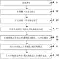
一种高功率密度IGZO薄膜晶体管的制造方法,包括以下步骤:A method for manufacturing a high power density IGZO thin film transistor, comprising the following steps:
S1 基板依次通过丙酮,乙醇以及去离子水在100 W功率下超声清洗10min;The S1 substrate was ultrasonically cleaned by acetone, ethanol and deionized water at a power of 100 W for 10 min in turn;
S2 在所述基板上采用等离子增强化学气相沉积(PECVD)工艺制备二氧化硅作为支撑层;S2 using a plasma enhanced chemical vapor deposition (PECVD) process to prepare silicon dioxide on the substrate as a support layer;
S3 在所述支撑层上采用直流溅射工艺制备金属钼(Mo)作为栅电极层;S3 using a DC sputtering process to prepare metal molybdenum (Mo) as a gate electrode layer on the support layer;
S4 在所述栅电极层上采用等离子增强化学气相沉积((PECVD)工艺形成栅绝缘层,随后在氮氧混合气氛下对栅绝缘层进行退火;S4 using a plasma enhanced chemical vapor deposition (PECVD) process to form a gate insulating layer on the gate electrode layer, and then annealing the gate insulating layer in a nitrogen-oxygen mixed atmosphere;
S5 在所述栅绝缘层上采用直流溅射工艺形成低阻有源层;S5 using a DC sputtering process to form a low-resistance active layer on the gate insulating layer;
S6 在所述低阻有源层上采用直流溅射工艺形成IGZO有源层,通过标准光刻工艺在低阻有源层和IGZO有源层外表面形成光刻胶阻挡层,将覆盖有所述光刻胶阻挡层的衬底使用浓度为1 mol/L的稀盐酸溶剂进行标准湿法刻蚀工艺,形成所述低阻有源层和所述IGZO有源层的目标图形,随后将去胶后图形化的低阻有源层以及IGZO有源层在空气氛围下退火30min,退火温度为250℃;S6 Using a DC sputtering process to form an IGZO active layer on the low-resistance active layer, and forming a photoresist barrier layer on the low-resistance active layer and the outer surface of the IGZO active layer by a standard photolithography process, which will cover The substrate of the photoresist barrier layer is subjected to a standard wet etching process using a dilute hydrochloric acid solvent with a concentration of 1 mol/L to form the target pattern of the low-resistance active layer and the IGZO active layer. The patterned low-resistance active layer and the IGZO active layer were annealed in air for 30 minutes, and the annealing temperature was 250°C;
S7 在所述IGZO有源层上表面的左侧和右侧采用电子束蒸发工艺形成源区电极层与漏区电极层;S7 using an electron beam evaporation process to form a source electrode layer and a drain electrode layer on the left and right sides of the upper surface of the IGZO active layer;
S8 在所述源区电极层、漏区电极层以及IGZO有源层上表面采用等离子增强化学气相沉积(PECVD)工艺形成钝化层,且钝化层形成后,在氧气氛围下进行退火。S8 A passivation layer is formed on the upper surfaces of the source electrode layer, the drain electrode layer and the IGZO active layer by a plasma enhanced chemical vapor deposition (PECVD) process, and after the passivation layer is formed, annealing is performed in an oxygen atmosphere.
进一步地,制备支撑层所用等离子增强化学气相沉积(PECVD)工艺的基底工艺温度为200℃,射频功率100 W, 反应压强为80 mtorr,在N2O: SiH4=600:100sccm混合气氛下进行制备。Further, the substrate process temperature of the plasma-enhanced chemical vapor deposition (PECVD) process used for preparing the support layer is 200 °C, the radio frequency power is 100 W, the reaction pressure is 80 mtorr, and the process is carried out in a mixed atmosphere of N2 O: SiH4 =600:100 sccm preparation.
进一步地,所述栅绝缘层的材质为氧化硅,所用等离子增强化学气相沉积(PECVD)工艺的基底工艺温度范围在300℃-380℃,射频功率100 W, 反应压强为50 mtorr,在N2O:SiH4=600:100sccm混合气氛下制备,随后在氮氧混合气氛为N2:O2=1000:400sccm下进行400℃退火30min处理。Further, the material of the gate insulating layer is silicon oxide, the substrate process temperature range of the plasma enhanced chemical vapor deposition (PECVD) process used is 300°C-380°C, the radio frequency power is 100 W, the reaction pressure is 50 mtorr, and the reaction pressure is 50 mtorr under N2 . It was prepared in a mixed atmosphere of O:SiH4 =600:100sccm, and then annealed at 400°C for 30min in a nitrogen-oxygen mixed atmosphere of N2 :O2 =1000:400sccm.
进一步地,步骤S5所述的低阻有源层的材质是氧化铟锌(IZO)半导体薄膜,所述氧化铟锌(IZO)半导体薄膜由氧化铟陶瓷靶材和氧化锌陶瓷靶通过共溅射工艺形成具有高载流子浓度(Nd-IZO>1e18cm-3)与高电子迁移率(μn-IZO>30cm2V-1s-1)的半导体薄膜;所述共溅射工艺在溅射功率为150 W、腔体压强为5 mtorr、腔体气氛为氩气或氩气和氧气混合的条件下制备,所述氩气和氧气的混合比例根据所制备的薄膜电阻率进行调节。Further, the material of the low-resistance active layer described in step S5 is an indium zinc oxide (IZO) semiconductor film, and the indium zinc oxide (IZO) semiconductor film is co-sputtered by an indium oxide ceramic target and a zinc oxide ceramic target. The process forms a semiconductor thin film with high carrier concentration (Nd-IZO >1e18cm-3 ) and high electron mobility (μn-IZO >30cm2 V-1 s-1 ); the co-sputtering process is in sputtering It was prepared under the conditions that the radiation power was 150 W, the cavity pressure was 5 mtorr, and the cavity atmosphere was argon or a mixture of argon and oxygen, and the mixing ratio of the argon and oxygen was adjusted according to the resistivity of the prepared film.
进一步地,步骤S6所述IGZO有源层是采用原位生长的方式制备;在所述低阻有源层制备完成后,随即采用直流溅射工艺在所述低阻有源层上表面进行IGZO半导体薄膜制备工艺, 所制备的IGZO有源层载流子浓度为1e15cm-3<Nd-IGZO<1e16cm-3,电子迁移率为5cm2V-1s-1<μn-IGZO<10cm2V-1s-1,以确保所制备的IGZO薄膜晶体管具有低关态电流(Ioff<1e-12A);步骤S6所述直流溅射工艺,选用原子比为In:Ga:Zn:O=2:2:1:7的铟镓锌氧陶瓷靶材,在基底加热温度为50℃、溅射功率为120 W、腔体压强为5 mtorr的条件下制备。Further, the IGZO active layer in step S6 is prepared by in-situ growth; after the preparation of the low-resistance active layer is completed, IGZO is immediately performed on the upper surface of the low-resistance active layer by a DC sputtering process. The semiconductor thin film preparation process, the carrier concentration of the prepared IGZO active layer is 1e15cm-3 <Nd-IGZO <1e16cm-3 , and the electron mobility is 5cm2 V-1 s-1 <μn-IGZO <10cm2 V-1 s-1 , to ensure that the prepared IGZO thin film transistor has a low off-state current (Ioff <1e-12 A); in the DC sputtering process in step S6, the atomic ratio is In:Ga:Zn:O The indium gallium zinc oxide ceramic target with a ratio of 2:2:1:7 was prepared under the conditions of a substrate heating temperature of 50 °C, a sputtering power of 120 W, and a cavity pressure of 5 mtorr.
进一步地,所述钝化层所用等离子增强化学气相沉积(PECVD)工艺的基底工艺温度为30℃,射频功率100 W, 反应压强为50 mtorr,在N2:SiH4 =600:60sccm混合气氛下进行;所述钝化层在氧气氛围下采用350℃退火3h。Further, the substrate process temperature of the plasma-enhanced chemical vapor deposition (PECVD) process used in the passivation layer is 30° C., the radio frequency power is 100 W, and the reaction pressure is 50 mtorr, under a mixed atmosphere of N2 : SiH4 =600:60sccm proceed; the passivation layer is annealed at 350° C. for 3h in an oxygen atmosphere.
有益效果:Beneficial effects:
1.采用具有高载流子浓度和高迁移率的金属氧化物IZO薄膜取代部分IGZO薄膜设于栅绝缘层上表面作为低阻有源层,有效提高漂移区载流子浓度,降低漂移区电阻;1. The metal oxide IZO film with high carrier concentration and high mobility is used to replace part of the IGZO film and set on the upper surface of the gate insulating layer as a low-resistance active layer, which effectively increases the carrier concentration in the drift region and reduces the resistance of the drift region. ;
2.精准调控IZO薄膜厚度,实现了兼顾高击穿电压和大输出电流的IGZO HVTFT;2. Precisely control the thickness of the IZO film, realizing the IGZO HVTFT with both high breakdown voltage and large output current;
3.在不增加工艺复杂度的前提下,对现有的IGZO偏移结构薄膜晶体管的输出电流实现了极大提升;3. Under the premise of not increasing the complexity of the process, the output current of the existing IGZO offset structure thin film transistor has been greatly improved;
4.一方面,IGZO有源层作为背沟道可以降低关态电流,减小功耗;另一方面,通过采用具有高载流子浓度的低阻层位于栅绝缘层上表面,作为正沟道层,有效降低了漏极偏移区域处漂移区电阻,输出电流密度能够提升至194%以上。4. On the one hand, the IGZO active layer as a back channel can reduce off-state current and power consumption; on the other hand, by using a low-resistance layer with high carrier concentration on the upper surface of the gate insulating layer, as a positive channel The channel layer effectively reduces the drift region resistance at the drain offset region, and the output current density can be increased to more than 194%.
附图说明Description of drawings
图1是现有的传统IGZO薄膜晶体管的结构示意图;1 is a schematic structural diagram of an existing traditional IGZO thin film transistor;
图2是带漏极偏移区IGZO薄膜晶体管的结构示意图;2 is a schematic structural diagram of an IGZO thin film transistor with a drain offset region;
图3是本发明实施例中IGZO薄膜晶体管的结构示意图;3 is a schematic structural diagram of an IGZO thin film transistor in an embodiment of the present invention;
图4是本发明实施例中IGZO薄膜晶体管的制备工艺流程图;Fig. 4 is the preparation process flow chart of IGZO thin film transistor in the embodiment of the present invention;
图5是本发明实施例中双有源层制备工艺流程;5 is a process flow for preparing a dual active layer in an embodiment of the present invention;
图6是本发明实施例与对比例的IGZO薄膜晶体管的输出特性曲线图;Fig. 6 is the output characteristic curve diagram of the IGZO thin film transistor of the embodiment of the present invention and a comparative example;
图7是本发明实施例与对比例的IGZO薄膜晶体管的功率密度比较图。FIG. 7 is a comparison diagram of the power density of the IGZO thin film transistor of the embodiment of the present invention and the comparative example.
附图说明标记:1-基板、2-支撑层、3-栅电极层、4-栅绝缘层、5-低阻有源层、6-IGZO有源层、7a-源区电极、7b-漏区电极、8-钝化层。Reference symbols: 1-substrate, 2-support layer, 3-gate electrode layer, 4-gate insulating layer, 5-low-resistance active layer, 6-IGZO active layer, 7a-source electrode, 7b-drain Area electrode, 8-passivation layer.
具体实施方式Detailed ways
下面的实施例可使本专业技术人员更全面地理解本发明,但不以任何方式限制本发明。The following examples may enable those skilled in the art to more fully understand the present invention, but do not limit the present invention in any way.
实施例1Example 1
一种高功率密度IGZO薄膜晶体管制造方法,包括以下步骤:A method for manufacturing a high power density IGZO thin film transistor, comprising the following steps:
S1 获取基板1S1 Get substrate 1
在本实施例中选用康宁Eagle XG玻璃基板,并依次通过丙酮,乙醇以及去离子水超声清洗处理,采用的超声功率是100 W,超声清洗的时间均为10分钟;In the present embodiment, Corning Eagle XG glass substrate is selected, and then ultrasonically cleaned with acetone, ethanol and deionized water in sequence, the ultrasonic power used is 100 W, and the ultrasonic cleaning time is 10 minutes;
S2 在所述基板1上表面形成支撑层2S2 Forming a
在本实施例中选用二氧化硅作为支撑层2,采用PECVD工艺在所述玻璃基板1上形成二氧化硅薄膜,其中,PECVD工艺条件设为基底温度200℃,射频功率100 W, 反应压强为80 mtorr,以及N2O:SiH4=600:100sccm的源气体氛围;In this embodiment, silicon dioxide is selected as the
S3在所述支撑层2上形成栅电极层3S3 forming a
在本实施例中选用导电金属钼(Mo)作为栅极金属电极,通过在所述支撑层2上采用标准光刻工艺,得到图形化的光刻胶掩膜层,随后通过直流溅射工艺在光刻胶掩膜层以及支撑层2上形成Mo膜,再通过标准剥离工艺,去除光刻胶后得到图形化的栅电极层3;In this embodiment, conductive metal molybdenum (Mo) is selected as the gate metal electrode, and a patterned photoresist mask layer is obtained by using a standard photolithography process on the
S4 在所述栅电极层3上形成栅绝缘层4S4 forming a
在本实施例中,选用二氧化硅作为栅绝缘层4,采用PECVD工艺在所述栅电极层3上形成栅绝缘层4,其中,PECVD工艺条件设为基底温度350℃,射频功率100 W, 反应压强为50mtorr,以及N2O:SiH4=600:100sccm源气体氛围,随后对所述栅绝缘层层在N2:O2=1000:400sccm混合氛围下进行400℃,退火半小时处理;In this embodiment, silicon dioxide is selected as the
S5 在所述栅绝缘层4上表面形成低阻有源层5S5 A low-resistance
在本发明实施例中,采用常温下的直流溅射工艺在栅绝缘层4的上表面形成IZO薄膜作为低阻有源层5,在本实施例中是选用氧化锌陶瓷靶、氧化铟陶瓷靶在溅射功率为150W、腔体压强为5 mtorr、腔体气氛比为Ar:O2=39.6:0.4sccm的工艺条件下进行共溅射形成IZO薄膜;In the embodiment of the present invention, an IZO film is formed on the upper surface of the
S6 在所述低阻有源层5上形成IGZO有源层6S6 forming an IGZO
在本发明实施例中,采用原位生长的方式通过直流溅射工艺在所述低阻有源层5上表面形成IGZO薄膜作为IGZO有源层6,在本实施例中是选用原子比为In:Ga:Zn:O=2:2:1:7的铟镓锌氧陶瓷靶材,在基底加热温度为50℃、溅射功率为120 W、腔体压强为5 mtorr的溅射工艺条件下制备IGZO薄膜;In the embodiment of the present invention, an IGZO thin film is formed on the upper surface of the low-resistance
采用标准光刻工艺在所述IGZO有源层6上表面形成光刻胶阻挡层,将覆盖有所述光刻胶阻挡层的衬底采用标准湿法刻蚀工艺形成所述低阻有源层5和所述IGZO有源层6的目标图形,湿法刻蚀工艺是采用浓度为1 mol/L的稀盐酸溶剂进行刻蚀工艺,随后将去胶后图形化的低阻有源层5以及IGZO有源层6在空气氛围下250℃退火半小时;A photoresist barrier layer is formed on the upper surface of the IGZO
S7 在所述IGZO有源层6上表面形成源区电极层7a和漏区电极层7bS7 Form a
在本发明实施例中,选用金属钛(Ti)作为源/漏区电极金属,通过标准光刻工艺在在所述IGZO有源层6上表面形成光刻胶掩膜层,随后,采用电子束蒸发工艺沉积金属钛(Ti),再通标准剥离工艺形成图形化的源区电极层7a、漏区电极层7b;In the embodiment of the present invention, titanium metal (Ti) is selected as the source/drain region electrode metal, and a photoresist mask layer is formed on the upper surface of the IGZO
S8 在所述IGZO有源层6上表面、所述源区电极层7a和漏区电极层7b上表面形成钝化层8S8 A
在本实施例中选用氮化硅作为钝化层8的材料,采用PECVD工艺形成钝化层8,PECVD工艺条件设为基底温度30℃,射频功率100 W, 反应压强为50 mtorr,以及N2:SiH4=600:60sccm源气体氛围,随后对所述氮化硅钝化层8在氧气氛围下进行350℃,退火三小时处理。In this embodiment, silicon nitride is selected as the material of the
对比例1Comparative Example 1
如图1所示,一种IGZO薄膜晶体管,包括玻璃基板、支撑层、栅电极层、栅绝缘层、IGZO有源层、源区电极层、漏区电极层、钝化层;所述支撑层完全覆盖于玻璃基板上,所述栅电极层设于支撑层中间,所述栅绝缘层完全覆盖栅电极层,左右两侧与支撑层上表面相连,所述IGZO有源层完全覆盖栅绝缘层,所述源区电极层、漏区电极层分别设于IGZO有源层左右两端,所述钝化层完全覆盖源区电极层、漏区电极层,并与IGZO有源层相连。As shown in Figure 1, an IGZO thin film transistor includes a glass substrate, a support layer, a gate electrode layer, a gate insulating layer, an IGZO active layer, a source electrode layer, a drain electrode layer, and a passivation layer; the support layer It completely covers the glass substrate, the gate electrode layer is arranged in the middle of the support layer, the gate insulating layer completely covers the gate electrode layer, the left and right sides are connected to the upper surface of the support layer, and the IGZO active layer completely covers the gate insulating layer. The source electrode layer and the drain electrode layer are respectively arranged on the left and right ends of the IGZO active layer, and the passivation layer completely covers the source electrode layer and the drain electrode layer, and is connected to the IGZO active layer.
对比例2Comparative Example 2
如图2所示,一种带漏极偏移区结构的IGZO薄膜晶体管,包括玻璃基板、支撑层、栅电极层、栅绝缘层、IGZO有源层、源区电极层、漏区电极层、钝化层;所述支撑层完全覆盖于玻璃基板上,所述栅电极层设于支撑层中间,所述栅绝缘层完全覆盖栅电极层,左右两侧与支撑层上表面相连,所述IGZO有源层完全覆盖栅绝缘层,所述源区电极层、漏区电极层分别设于IGZO有源层左右两端,所述漏区电极层在水平位置上与栅电极层存在2μm的非交叠区域,该非交叠区域构成漏极偏移区;所述钝化层完全覆盖源区电极层、漏区电极层,并与IGZO有源层相连。As shown in FIG. 2, an IGZO thin film transistor with a drain offset region structure includes a glass substrate, a support layer, a gate electrode layer, a gate insulating layer, an IGZO active layer, a source electrode layer, a drain electrode layer, Passivation layer; the support layer completely covers the glass substrate, the gate electrode layer is arranged in the middle of the support layer, the gate insulating layer completely covers the gate electrode layer, the left and right sides are connected to the upper surface of the support layer, the IGZO The active layer completely covers the gate insulating layer, the source electrode layer and the drain electrode layer are respectively arranged at the left and right ends of the IGZO active layer, and the drain electrode layer and the gate electrode layer have a non-intersection of 2 μm in the horizontal position. The non-overlapping region constitutes the drain offset region; the passivation layer completely covers the source electrode layer and the drain electrode layer, and is connected to the IGZO active layer.
图5是本发明实施中双有源层制备工艺流程;5 is a process flow for preparing a dual active layer in the implementation of the present invention;
图6是本发明实施例与对比例的IGZO薄膜晶体管的输出特性曲线,其中,对比例1是现有传统结构的IGZO薄膜晶体管,对比例2是现有带漏极偏移区结构的IGZO薄膜晶体管,由于IGZO漂移区中较低的载流子浓度会增加导通电阻,降低输出电流,显然,对比例2的输出电流相较于对比例1降低了59.2% (Id,offset=13.5 μA,Id,con=21.5 μA)。6 is the output characteristic curve of the IGZO thin film transistor according to the embodiment of the present invention and the comparative example, wherein, the comparative example 1 is an IGZO thin film transistor with a conventional structure, and the comparative example 2 is an IGZO thin film with a drain offset region structure. For the transistor, the lower carrier concentration in the IGZO drift region will increase the on-resistance and reduce the output current. Obviously, the output current of Comparative Example 2 is reduced by 59.2% compared to Comparative Example 1 (Id,offset =13.5 μA ,Id,con =21.5 μA).
然而,在本发明实施例中,通过采用具有高载流子浓度和高电子迁移率的低阻有源层5设于栅绝缘层4上表面,取代部分传统的IGZO有源层结构,显著提高了漂移区载流子浓度,降低了漂移区电阻,此外,由于IZO薄膜具有高电子迁移率,实施例的输出电流相较于对比例1提升了194% (Id,DAL=63.2 μA,Id,con=21.5 μA)。However, in the embodiment of the present invention, a low-resistance
图7是本发明实施例与对比例的IGZO薄膜晶体管的功率密度比较图,其中,对比例1是现有传统结构的IGZO薄膜晶体管,对比例2是现有带漏极偏移区结构的IGZO薄膜晶体管,对于对比例1,漏区电极与栅电极之间的交叠区在高漏极电压下会发生电场聚集,栅绝缘层中高的电场峰值导致薄膜晶体管过早击穿,对比例1的击穿电压为72 V。7 is a power density comparison diagram of an IGZO thin film transistor according to an embodiment of the present invention and a comparative example, wherein the comparative example 1 is an IGZO thin film transistor with a conventional structure, and the comparative example 2 is an IGZO with a drain offset region structure. For the thin film transistor, for Comparative Example 1, electric field accumulation occurs in the overlap region between the drain electrode and the gate electrode at high drain voltage, and the high electric field peak in the gate insulating layer causes the thin film transistor to break down prematurely. The breakdown voltage is 72 V.
在对比例2和本实施例中,由于漏区电极与栅电极在水平位置上存在1 μm的非交叠区,有效缓解了栅电极右侧末端附近的电场聚集现象,两种结构均实现了较高的击穿电压,分别为380 V和384 V,但值得注意的是,结合图5,对比例2中具有高阻值的IGZO漂移区会导致对比例2的输出电流降低,相反的,在本发明实施例中采用的低阻有源层5叠加IGZO有源层6的结构,不仅弥补了漂移区对输出电流的恶化效应,还因IZO薄膜具有高的电子迁移率,显著提高了输出电流(相较于对比例1)。据此,本发明实施例的功率密度相较于对比例1和对比例2分别提高了231.2%和1456.3%,实现了具有高功率密度的IGZO功率器件。In Comparative Example 2 and this example, since there is a 1 μm non-overlapping region between the drain electrode and the gate electrode in the horizontal position, the electric field accumulation near the right end of the gate electrode is effectively alleviated. The higher breakdown voltages, 380 V and 384 V, respectively, but it is worth noting that, in conjunction with Figure 5, the IGZO drift region with high resistance in Comparative Example 2 will cause the output current of Comparative Example 2 to decrease, conversely, The structure of the low-resistance
Claims (10)
Translated fromChinesePriority Applications (1)
| Application Number | Priority Date | Filing Date | Title |
|---|---|---|---|
| CN202210672734.9ACN115132848B (en) | 2022-06-15 | 2022-06-15 | High-power-density IGZO thin film transistor and manufacturing method thereof |
Applications Claiming Priority (1)
| Application Number | Priority Date | Filing Date | Title |
|---|---|---|---|
| CN202210672734.9ACN115132848B (en) | 2022-06-15 | 2022-06-15 | High-power-density IGZO thin film transistor and manufacturing method thereof |
Publications (2)
| Publication Number | Publication Date |
|---|---|
| CN115132848Atrue CN115132848A (en) | 2022-09-30 |
| CN115132848B CN115132848B (en) | 2024-06-14 |
Family
ID=83378808
Family Applications (1)
| Application Number | Title | Priority Date | Filing Date |
|---|---|---|---|
| CN202210672734.9AActiveCN115132848B (en) | 2022-06-15 | 2022-06-15 | High-power-density IGZO thin film transistor and manufacturing method thereof |
Country Status (1)
| Country | Link |
|---|---|
| CN (1) | CN115132848B (en) |
Cited By (3)
| Publication number | Priority date | Publication date | Assignee | Title |
|---|---|---|---|---|
| CN115458609A (en)* | 2022-10-11 | 2022-12-09 | 东南大学 | A high withstand voltage, low on-resistance IGZO thin film transistor and its preparation method |
| CN119008705A (en)* | 2024-10-24 | 2024-11-22 | 南京邮电大学 | Amorphous InGaZnO/InAlSnO heterojunction composite channel double-gate thin film transistor device and preparation method thereof |
| WO2025044156A1 (en)* | 2023-08-29 | 2025-03-06 | 东南大学 | Ito thin-film transistor with high withstand voltage and low on-resistance, and preparation method therefor |
Citations (3)
| Publication number | Priority date | Publication date | Assignee | Title |
|---|---|---|---|---|
| CN105006487A (en)* | 2015-07-14 | 2015-10-28 | 北京大学 | Top gate self-aligned metal oxide semiconductor thin-film transistor and preparation method thereof |
| CN113270501A (en)* | 2021-05-19 | 2021-08-17 | 东南大学 | Power IGZO thin film transistor and preparation method thereof |
| CN113594260A (en)* | 2021-07-22 | 2021-11-02 | 东南大学 | IGZO thin film transistor and manufacturing method thereof |
- 2022
- 2022-06-15CNCN202210672734.9Apatent/CN115132848B/enactiveActive
Patent Citations (3)
| Publication number | Priority date | Publication date | Assignee | Title |
|---|---|---|---|---|
| CN105006487A (en)* | 2015-07-14 | 2015-10-28 | 北京大学 | Top gate self-aligned metal oxide semiconductor thin-film transistor and preparation method thereof |
| CN113270501A (en)* | 2021-05-19 | 2021-08-17 | 东南大学 | Power IGZO thin film transistor and preparation method thereof |
| CN113594260A (en)* | 2021-07-22 | 2021-11-02 | 东南大学 | IGZO thin film transistor and manufacturing method thereof |
Cited By (4)
| Publication number | Priority date | Publication date | Assignee | Title |
|---|---|---|---|---|
| CN115458609A (en)* | 2022-10-11 | 2022-12-09 | 东南大学 | A high withstand voltage, low on-resistance IGZO thin film transistor and its preparation method |
| WO2024078637A1 (en)* | 2022-10-11 | 2024-04-18 | 东南大学 | High-voltage-resistance and low-on-resistance igzo thin-film transistor and preparation method therefor |
| WO2025044156A1 (en)* | 2023-08-29 | 2025-03-06 | 东南大学 | Ito thin-film transistor with high withstand voltage and low on-resistance, and preparation method therefor |
| CN119008705A (en)* | 2024-10-24 | 2024-11-22 | 南京邮电大学 | Amorphous InGaZnO/InAlSnO heterojunction composite channel double-gate thin film transistor device and preparation method thereof |
Also Published As
| Publication number | Publication date |
|---|---|
| CN115132848B (en) | 2024-06-14 |
Similar Documents
| Publication | Publication Date | Title |
|---|---|---|
| CN115132848B (en) | High-power-density IGZO thin film transistor and manufacturing method thereof | |
| CN106128963B (en) | Thin film transistor (TFT) and preparation method, array substrate and preparation method, display panel | |
| US7883934B2 (en) | Method of fabricating oxide semiconductor device | |
| US9991135B2 (en) | Method for fabricating a metal oxide thin film transistor | |
| WO2011143887A1 (en) | Metal oxide thin film transistor and manufacturing method thereof | |
| WO2020228180A1 (en) | Array substrate and preparation method for array substrate | |
| CN111446288A (en) | NS-stacked transistor based on two-dimensional material and preparation method thereof | |
| WO2024078637A1 (en) | High-voltage-resistance and low-on-resistance igzo thin-film transistor and preparation method therefor | |
| JP2018074178A (en) | Method for manufacturing thin-film transistor | |
| WO2021073193A1 (en) | Composite crystalline metal oxide thin film transistor having vertical structure and manufacturing method therefor | |
| WO2021134423A1 (en) | Method for preparing thin film transistor | |
| CN115084276B (en) | Amorphous oxide semiconductor thin film transistor and preparation method thereof | |
| CN109148597A (en) | Thin film transistor (TFT) and preparation method thereof | |
| CN116504815B (en) | A high-power a-IGZO thin film transistor and its preparation method | |
| CN110634957A (en) | TFT device and preparation method thereof, TFT array substrate, and display device | |
| WO2014153853A1 (en) | Thin film transistor and manufacturing method thereof, array substrate and display device | |
| CN110808289A (en) | Top gate Schottky oxide thin film transistor and preparation method thereof | |
| KR102685952B1 (en) | Thin film transistor including spinel single-phase crystalline izto oxide semiconductor | |
| CN116314197A (en) | Oxide semiconductor three-dimensional integrated cascode enhanced GaN power device and manufacturing method | |
| KR101231724B1 (en) | Thinfilm transistor and method of manufacturing thereof | |
| WO2023241006A1 (en) | Phase inverter based on igzo thin-film transistor, and preparation method therefor | |
| WO2021134422A1 (en) | Method for fabricating thin film transistor | |
| CN112687554B (en) | Array substrate preparation method, array substrate and display device | |
| KR102855270B1 (en) | Thin Film Transistor with Trench-structured Oxide Semiconductor Layer and Method for Manufacturing the Same | |
| CN107749422A (en) | Oxide semiconductor thin-film transistor |
Legal Events
| Date | Code | Title | Description |
|---|---|---|---|
| PB01 | Publication | ||
| PB01 | Publication | ||
| SE01 | Entry into force of request for substantive examination | ||
| SE01 | Entry into force of request for substantive examination | ||
| GR01 | Patent grant | ||
| GR01 | Patent grant |