CN115117146A - SiC-based schottky device with low conduction voltage drop and preparation method thereof - Google Patents
SiC-based schottky device with low conduction voltage drop and preparation method thereofDownload PDFInfo
- Publication number
- CN115117146A CN115117146ACN202210532495.7ACN202210532495ACN115117146ACN 115117146 ACN115117146 ACN 115117146ACN 202210532495 ACN202210532495 ACN 202210532495ACN 115117146 ACN115117146 ACN 115117146A
- Authority
- CN
- China
- Prior art keywords
- drift layer
- layer
- sic
- low
- drift
- Prior art date
- Legal status (The legal status is an assumption and is not a legal conclusion. Google has not performed a legal analysis and makes no representation as to the accuracy of the status listed.)
- Granted
Links
Images


Classifications
- H—ELECTRICITY
- H10—SEMICONDUCTOR DEVICES; ELECTRIC SOLID-STATE DEVICES NOT OTHERWISE PROVIDED FOR
- H10D—INORGANIC ELECTRIC SEMICONDUCTOR DEVICES
- H10D8/00—Diodes
- H10D8/60—Schottky-barrier diodes
- H—ELECTRICITY
- H10—SEMICONDUCTOR DEVICES; ELECTRIC SOLID-STATE DEVICES NOT OTHERWISE PROVIDED FOR
- H10D—INORGANIC ELECTRIC SEMICONDUCTOR DEVICES
- H10D62/00—Semiconductor bodies, or regions thereof, of devices having potential barriers
- H10D62/10—Shapes, relative sizes or dispositions of the regions of the semiconductor bodies; Shapes of the semiconductor bodies
- H10D62/102—Constructional design considerations for preventing surface leakage or controlling electric field concentration
- H10D62/112—Constructional design considerations for preventing surface leakage or controlling electric field concentration for preventing surface leakage due to surface inversion layers, e.g. by using channel stoppers
- H—ELECTRICITY
- H10—SEMICONDUCTOR DEVICES; ELECTRIC SOLID-STATE DEVICES NOT OTHERWISE PROVIDED FOR
- H10D—INORGANIC ELECTRIC SEMICONDUCTOR DEVICES
- H10D62/00—Semiconductor bodies, or regions thereof, of devices having potential barriers
- H10D62/10—Shapes, relative sizes or dispositions of the regions of the semiconductor bodies; Shapes of the semiconductor bodies
- H10D62/124—Shapes, relative sizes or dispositions of the regions of semiconductor bodies or of junctions between the regions
- H—ELECTRICITY
- H10—SEMICONDUCTOR DEVICES; ELECTRIC SOLID-STATE DEVICES NOT OTHERWISE PROVIDED FOR
- H10D—INORGANIC ELECTRIC SEMICONDUCTOR DEVICES
- H10D62/00—Semiconductor bodies, or regions thereof, of devices having potential barriers
- H10D62/80—Semiconductor bodies, or regions thereof, of devices having potential barriers characterised by the materials
- H10D62/83—Semiconductor bodies, or regions thereof, of devices having potential barriers characterised by the materials being Group IV materials, e.g. B-doped Si or undoped Ge
- H10D62/832—Semiconductor bodies, or regions thereof, of devices having potential barriers characterised by the materials being Group IV materials, e.g. B-doped Si or undoped Ge being Group IV materials comprising two or more elements, e.g. SiGe
- H10D62/8325—Silicon carbide
- H—ELECTRICITY
- H10—SEMICONDUCTOR DEVICES; ELECTRIC SOLID-STATE DEVICES NOT OTHERWISE PROVIDED FOR
- H10D—INORGANIC ELECTRIC SEMICONDUCTOR DEVICES
- H10D8/00—Diodes
- H10D8/01—Manufacture or treatment
- H10D8/051—Manufacture or treatment of Schottky diodes
Landscapes
- Electrodes Of Semiconductors (AREA)
Abstract
Translated fromChinese
Description
Translated fromChinese技术领域technical field
本发明涉及一种SiC肖特基器件及其制备方法,尤其是涉及一种具有低导通压降的SiC基肖特基二极管结构及其制备方法。The invention relates to a SiC Schottky device and a preparation method thereof, in particular to a SiC-based Schottky diode structure with low conduction voltage drop and a preparation method thereof.
背景技术Background technique
第三代半导体碳化硅(SiC)材料具有比传统的Si材料优异的物理和电学特性。例如SiC具有禁带宽、热导率高、击穿场强高、饱和电子漂移速率高等特点,同时还兼具有极好的物理及化学稳定性、极强的抗辐照能力和机械强度等。因此,基于宽禁带SiC材料的电子器件可用于高温、大功率、高频、高辐射等电力电子领域。The third generation semiconductor silicon carbide (SiC) materials have superior physical and electrical properties than traditional Si materials. For example, SiC has the characteristics of band gap, high thermal conductivity, high breakdown field strength, high saturation electron drift rate, and also has excellent physical and chemical stability, strong radiation resistance and mechanical strength. Therefore, electronic devices based on wide-bandgap SiC materials can be used in power electronics fields such as high temperature, high power, high frequency, and high radiation.
SiC肖特基二极管器件在商业化进程上已经很成熟,尤其以注入p型屏蔽层的结型肖特基器件为主流。结势垒型肖特基二极管将PN结集成在肖特基结构中,能够有效地保证低肖特基势垒的优良正向导通特性,同时在反向阻断时,能够将最大电场限制在PN结区从而降低表面肖特基接触处的电场,使得反向漏电流相对于纯肖特基类型的大大降低。尽管如此,一方面,SiC肖特基器件的导通压降(VF)受到总串联电阻的影响,即总串联电阻包括JFET电阻RJFET、漂移区电阻Rdrift以及衬底电阻RSUB。针对SiC肖特基器件阻断电压与正向导通特性折中设计仍然存在着诸多矛盾点,例如对其产生关键影响的外延层掺杂和厚度的优化设计,较高的漂移区掺杂和较小的漂移层厚度不利于反向阻断能力的提升,反之,不利于正向导通特性的提升。另一方面,SiC衬底表面依然存在较多缺陷,虽然通过生长缓冲层来提高后续外延层的质量,但器件通电后依然存在着较强电应力的驱动作用,使得缺陷演化进而影响到器件的整体可靠性。考虑到这些因素需要寻找一种新的技术使得SiC肖特基器件具有低导通压降,同时能够降低敏感区域的缺陷扩展并提高器件的长期稳定性工作能力。SiC Schottky diode devices are already very mature in the commercialization process, especially the junction Schottky devices injected into the p-type shielding layer are the mainstream. Junction-barrier Schottky diode integrates PN junction in Schottky structure, which can effectively ensure the excellent forward conduction characteristics of low Schottky barrier, and can limit the maximum electric field to The PN junction region thus reduces the electric field at the surface Schottky contact, resulting in a greatly reduced reverse leakage current relative to the pure Schottky type. Nonetheless, on the one hand, the on-voltage drop (VF ) of a SiC Schottky device is affected by the total series resistance, ie the total series resistance includes the JFET resistance RJFET , the drift region resistance Rdrift and the substrate resistance RSUB . There are still many contradictions in the compromise design between blocking voltage and forward conduction characteristics of SiC Schottky devices, such as the optimal design of epitaxial layer doping and thickness that have a key impact on it, higher drift region doping and relatively A small drift layer thickness is not conducive to the improvement of the reverse blocking capability, and conversely, it is not conducive to the improvement of the forward conduction characteristics. On the other hand, there are still many defects on the surface of the SiC substrate. Although the quality of the subsequent epitaxial layer is improved by growing the buffer layer, there is still a strong electrical stress driving effect after the device is energized, which makes the evolution of the defects affect the device's performance. overall reliability. Considering these factors, it is necessary to find a new technology to make SiC Schottky devices have low on-voltage drop, at the same time, it can reduce the defect propagation in sensitive areas and improve the long-term stability of the device.
发明内容SUMMARY OF THE INVENTION
针对上述问题,本发明的目的在于,针对目前SiC肖特基器件的导通压降和阻断电压的设计矛盾体、以及材料缺陷受电应力扩展的问题,提供一种SiC肖特基器件的结构设计方案与制备方法,主要用于降低SiC肖特基器件的导通压降和功耗,同时提高器件长期稳定性。In view of the above-mentioned problems, the purpose of the present invention is to provide a kind of SiC Schottky device in view of the current design contradictions of the on-voltage drop and blocking voltage of the SiC Schottky device, as well as the expansion of the electrical stress of the material defects. The structural design scheme and the preparation method are mainly used to reduce the turn-on voltage drop and power consumption of the SiC Schottky device, and at the same time improve the long-term stability of the device.
本发明的技术方案是从决定SiC肖特基器件导通压降的总串联电阻如JFET电阻RJFET、漂移区电阻Rdrift以及衬底电阻RSUB等方面综合考虑,提出一种具有变掺杂外延结构的SiC肖特基器件,利用远离主结区的高掺杂漂移层降低器件的串联电阻,并利用主结区域的低掺杂层提高p型屏蔽层的保护作用,降低器件的反向漏电流,同时利用靠近缓冲层一侧低掺杂外延结构设计以提高SiC肖特基器件的可靠性工作能力。The technical scheme of the present invention is to comprehensively consider the total series resistance that determines the on-voltage drop of the SiC Schottky device, such as the JFET resistance RJFET , the drift region resistance Rdrift and the substrate resistance RSUB , etc. For SiC Schottky devices with epitaxial structure, the highly doped drift layer away from the main junction area is used to reduce the series resistance of the device, and the low doped layer in the main junction area is used to improve the protection of the p-type shielding layer and reduce the reverse direction of the device. At the same time, the low-doped epitaxial structure design near the buffer layer is used to improve the reliability of the SiC Schottky device.
为了实现以上目的,本发明的技术方案为:In order to achieve the above purpose, the technical scheme of the present invention is:
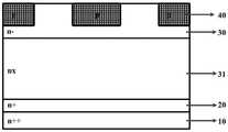
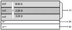
一种具有低导通压降的SiC基肖特基器件,由下至上包括欧姆接触电极、n++型SiC衬底基片、n+型缓冲层、漂移层和肖特基接触电极;漂移层自下而上包括nx第一漂移层和n-第二漂移层,nx第一漂移层的掺杂浓度大于n-第二漂移层的掺杂浓度,n-第二漂移层之内设有p型屏蔽层;其中nx第一漂移层的掺杂浓度自下而上先由低变至高掺杂,后由高变至低掺杂。A SiC-based Schottky device with low on-voltage drop, from bottom to top, includes an ohmic contact electrode, an n++ type SiC substrate substrate, an n+ type buffer layer, a drift layer and a Schottky contact electrode; the drift layer is from bottom to top The upper part includes an nx first drift layer and an n- second drift layer, the doping concentration of the nx first drift layer is greater than that of the n- second drift layer, and a p-type shield is arranged in the n- second drift layer. layer; wherein the doping concentration of the nx first drift layer first changes from low to high doping from bottom to top, and then changes from high to low doping.
可选的,所述nx第一漂移层的厚度占比整个漂移层厚度的50-80%。Optionally, the thickness of the nx first drift layer accounts for 50-80% of the thickness of the entire drift layer.
可选的,所述p型屏蔽层设于所述n-第二漂移层的上部,且所述p型屏蔽层的底部与所述n-第二漂移层的底部的间距是n-第二漂移层厚度的50%~90%。Optionally, the p-type shielding layer is provided on the upper part of the n-second drift layer, and the distance between the bottom of the p-type shielding layer and the bottom of the n-second drift layer is n-second 50% to 90% of the thickness of the drift layer.
可选的,所述nx第一漂移层包括叠设的至少三个掺杂层,且中间的掺杂层的掺杂浓度大于上下两侧的掺杂层的掺杂浓度。Optionally, the nx first drift layer includes at least three stacked doping layers, and the doping concentration of the middle doping layer is greater than the doping concentration of the doping layers on the upper and lower sides.
可选的,所述中间的掺杂层的厚度占比所述nx第一漂移层厚度的40%~60%。Optionally, the thickness of the intermediate doped layer accounts for 40% to 60% of the thickness of the nx first drift layer.
可选的,所述nx第一漂移层由下至上形成渐变掺杂,且掺杂浓度先由低至高,再由高至低。Optionally, the nx first drift layer is gradually doped from bottom to top, and the doping concentration is first from low to high, and then from high to low.
可选的,所述nx第一漂移层的掺杂浓度最高不超过1×1017cm-3,最低不少于1×1015cm-3;所述n-第二漂移层的掺杂浓度范围为1×10¹⁴~5×1015cm-3;所述n+型缓冲层的掺杂浓度范围为1×10¹⁸~1×1019cm-3。Optionally, the doping concentration of the nx first drift layer is not more than 1×1017 cm-3 at the highest, and not less than 1×1015 cm-3 at the lowest; the doping concentration of the n-second drift layer The range is 1×10¹⁴ to 5×1015 cm−3 ; the doping concentration of the n+ type buffer layer is in the range of 1×10¹⁸ to 1×1019 cm−3 .
一种上述具有低导通压降的SiC基肖特基器件的制备方法,包括以下步骤:A preparation method of the above-mentioned SiC-based Schottky device with low on-voltage drop, comprising the following steps:
1)于n++型SiC衬底基片之上生长n+型缓冲层;1) growing an n+ type buffer layer on the n++ type SiC substrate;
2)生长漂移层,首先于n+型缓冲层之上生长掺杂浓度较高的nx第一漂移层,然后于nx第一漂移层上生长掺杂浓度较低的n-第二漂移层;2) growing a drift layer, firstly growing an nx first drift layer with a higher doping concentration on the n+ type buffer layer, and then growing an n- second drift layer with a lower doping concentration on the nx first drift layer;
3)通过局部掺杂工艺于n-第二漂移层中制作p型屏蔽层;3) forming a p-type shielding layer in the n-second drift layer through a local doping process;
4)于n++型SiC衬底基片背面制作欧姆接触电极;4) Making ohmic contact electrodes on the back of the n++ type SiC substrate;
5)于n-第二漂移层上制作肖特基接触电极。5) A Schottky contact electrode is formed on the n-second drift layer.
可选的,所述步骤2)中,采用化学气相沉积工艺生长所述漂移层,生长温度为1500-1700℃,掺杂源为NH3,通过控制掺杂源流量控制掺杂浓度。Optionally, in the step 2), the drift layer is grown by a chemical vapor deposition process, the growth temperature is 1500-1700° C., the doping source is NH3 , and the doping concentration is controlled by controlling the flow of the doping source.
可选的,所述nx第一漂移层生长过程中,所述掺杂源的流量阶段式变化或渐变式变化。Optionally, during the growth process of the nx first drift layer, the flow rate of the doping source is changed in stages or gradually.
本发明的有益效果为:The beneficial effects of the present invention are:
(1)基于部分高掺杂的漂移层,使得SiC肖特基器件的串联电阻大大降低;(1) Based on part of the highly doped drift layer, the series resistance of SiC Schottky devices is greatly reduced;
(2)采用变掺杂外延结构,主结区域的低掺杂层仍能提高p型屏蔽层的保护作用,降低器件的反向漏电流,提高SiC肖特基器件的阻断能力。(2) Using the variable doping epitaxial structure, the low-doped layer in the main junction region can still improve the protection of the p-type shielding layer, reduce the reverse leakage current of the device, and improve the blocking ability of the SiC Schottky device.
(3)采用变掺杂外延结构,远离主结区域的高掺杂层可以适当地减小厚度,与传统器件相比进一步降低器件导通压降;(3) By adopting the variable doping epitaxial structure, the thickness of the highly doped layer far from the main junction region can be appropriately reduced, and the on-voltage drop of the device can be further reduced compared with the traditional device;
(4)采用变掺杂外延结构,靠近缓冲层一侧的掺杂层可以降低缓冲层与外延层界面的电场和碰撞电离率等,减小缺陷扩展的几率。(4) The variable doping epitaxial structure is adopted, and the doping layer near the buffer layer can reduce the electric field and impact ionization rate at the interface between the buffer layer and the epitaxial layer, and reduce the probability of defect expansion.
(5)所述的SiC肖特基器件,相比于传统的肖特基二极管,具有更高的巴俐加优值和更大的高频开关优值。(5) Compared with the traditional Schottky diode, the SiC Schottky device has a higher figure of merit of Barriga and a larger figure of merit of high-frequency switching.
附图说明Description of drawings
图1本公开提供的一种低导通压降的SiC肖特基器件的制备流程图;1 is a flow chart of the preparation of a SiC Schottky device with low on-voltage drop provided by the present disclosure;
图2是实施例涉及的SiC外延材料基片的结构图;Fig. 2 is the structural diagram of the SiC epitaxial material substrate involved in the embodiment;
图3是实施例涉及的制成nx第一漂移层31的结构图;FIG. 3 is a structural diagram of an nx
图4是实施例涉及的制成n-第二漂移层30的结构图;FIG. 4 is a structural diagram of an n-
图5是实施例涉及的制成p型屏蔽层40的结构图;FIG. 5 is a structural diagram of the p-
图6是实施例涉及的制成欧姆接触电极50的结构图;FIG. 6 is a structural diagram of an
图7是实施例涉及的制成肖特基接触电极60的结构图;FIG. 7 is a structural diagram of a
图8是实施例涉及的制成nx第一漂移层31的结构图;FIG. 8 is a structural diagram of making an nx
图9是实施例二涉及的制成低导通压降的SiC肖特基器件的结构图;FIG. 9 is a structural diagram of a SiC Schottky device with a low on-state voltage drop involved in
图10是实施例二涉及的制成nx第一漂移层31的结构图;FIG. 10 is a structural diagram of the nx
图11是实施例二涉及的制成低导通压降的SiC肖特基器件的结构图;FIG. 11 is a structural diagram of a SiC Schottky device with a low on-state voltage drop involved in
图12是本发明实施例低导通压降的SiC肖特基器件与传统器件的对比效果图。FIG. 12 is a comparison effect diagram of a SiC Schottky device with low on-voltage drop according to an embodiment of the present invention and a conventional device.
具体实施方式Detailed ways
以下结合附图和具体实施例对本发明做进一步解释。本发明的各附图仅为示意以更容易了解本发明,其具体比例可依照设计需求进行调整。文中所描述的图形中相对元件的上下关系以及正面/背面的定义,在本领域技术人员应能理解是指构件的相对位置而言,因此皆可以翻转而呈现相同的构件,此皆应同属本说明书所揭露的范围。The present invention will be further explained below with reference to the accompanying drawings and specific embodiments. The accompanying drawings of the present invention are only schematic diagrams to facilitate the understanding of the present invention, and the specific proportions thereof can be adjusted according to design requirements. Those skilled in the art should understand that the upper and lower relationship of the relative elements in the graphics described in the text and the definition of the front/back surface refer to the relative positions of the components, so they can all be turned over to present the same components, which shall belong to the same category. the scope disclosed in the specification.
本发明中,提供一种兼具低导通压降和高可靠性的SiC肖特基器件结构及制备方法。器件利用变掺杂外延结构,大大降低SiC肖特基器件的漂移层电阻,保证器件正向导通时具有低导通压降特性。反向阻断时,相邻p型屏蔽层的自洽屏蔽作用有效保护肖特基接触,使得器件肖特基接触处电场大大降低,雪崩发生在器件体区的PN结处,同时靠近缓冲层一侧的外延层区域的电应力降低,提高了器件的可靠性。所制备的SiC肖特基器件具有较低的正向导通压降和较低的反向漏电电流,器件的导通、阻断特性以及稳定性均得到提高。In the present invention, a SiC Schottky device structure and preparation method are provided with both low on-state voltage drop and high reliability. The device uses a variable doping epitaxial structure, which greatly reduces the drift layer resistance of the SiC Schottky device and ensures that the device has low on-voltage drop characteristics when it is conducting forward. When reverse blocking, the self-consistent shielding effect of the adjacent p-type shielding layer effectively protects the Schottky contact, so that the electric field at the Schottky contact of the device is greatly reduced, and the avalanche occurs at the PN junction of the device body region and close to the buffer layer. The electrical stress of the epitaxial layer region on one side is reduced, and the reliability of the device is improved. The prepared SiC Schottky device has lower forward voltage drop and lower reverse leakage current, and the turn-on, blocking characteristics and stability of the device are improved.
实施例1Example 1
图1是一种低导通压降的SiC肖特基器件的制备方法流程图,包括以下步骤:Figure 1 is a flow chart of a method for preparing a SiC Schottky device with low on-voltage drop, including the following steps:
S1.清洗SiC材料基片。S1. Cleaning the SiC material substrate.
S2.生长缓冲层。S2. Growth buffer layer.
S3.生长漂移层。S3. Growing the drift layer.
S4.制作p型屏蔽层。S4. Make a p-type shielding layer.
S5.制作欧姆接触。S5. Making ohmic contacts.
S6.制作肖特基接触。S6. Making Schottky contacts.
其中,in,
步骤S1:清洗SiC材料基片。所述的SiC材料基片包含的n++型SiC衬底基片10,对该基片样品进行标准清洗,具体为:Step S1: cleaning the SiC material substrate. The n++ type
a.依次用丙酮和乙醇超声清洗三遍,再用去离子水冲洗。a. Sequentially wash with acetone and ethanol three times ultrasonically, and then rinse with deionized water.
b.将将有机超声后的SiC外延材料基片放入放在浓硫酸和双氧水溶液中至少煮10min。b. Put the SiC epitaxial material substrate after organic ultrasound into concentrated sulfuric acid and hydrogen peroxide solution and cook for at least 10min.
c.将煮过浓硫酸的SiC外延材料基片依次用一号液和二号液煮15min,再用去离子水冲洗干净后用氮气吹干待用。一号液为氨水、过氧化氢和去离子水的混合液,按体积比氨水︰过氧化氢︰去离子水=1︰2︰5,二号液为盐酸、过氧化氢和去离子水的混合液,按体积比盐酸︰过氧化氢︰去离子水=1︰2︰5。c. Boil the SiC epitaxial material substrate that has been boiled with concentrated sulfuric acid with No. 1 solution and No. 2 solution for 15 minutes, rinse it with deionized water, and dry it with nitrogen for use. No. 1 solution is a mixture of ammonia water, hydrogen peroxide and deionized water. The volume ratio of ammonia water: hydrogen peroxide: deionized water = 1:2:5. No. 2 solution is hydrochloric acid, hydrogen peroxide and deionized water. Mixed solution, hydrochloric acid: hydrogen peroxide: deionized water = 1:2:5 by volume.
d.将冲洗后的SiC外延材料基片放入稀释的氢氟酸(按体积比氟化氢:去离子水=1:3)内浸泡1min,去除表面的氧化物,并用去离子水清洗,再烘干。d. Put the rinsed SiC epitaxial material substrate into diluted hydrofluoric acid (by volume hydrogen fluoride: deionized water = 1:3) and soak for 1 min to remove oxides on the surface, rinse with deionized water, and bake again Dry.
步骤S2:生长缓冲层。如图2所示,所述的n+型缓冲层20为同质材料,具体包括:Step S2: growing the buffer layer. As shown in FIG. 2 , the n+
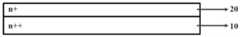
如图2所示,通过物理或者化学气相沉积获得,具体为:利用化学气相沉积或物理气相沉积等方法将同质材料n+型缓冲层20生长到清洗后的SiC材料基片的n++型SiC衬底基片10之上,生长源为SiH4和C2H4,或者其他Si源和C源气体,n+型缓冲层20的厚度为0.5-5μm,n+型缓冲层20的生长温度为1500-1700℃,掺杂源为NH3。n+型缓冲层20的掺杂浓度范围为1×10¹⁸~1×1019cm-3。As shown in FIG. 2, it is obtained by physical or chemical vapor deposition, specifically: using chemical vapor deposition or physical vapor deposition and other methods to grow the n+-
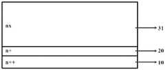
步骤S3:生长漂移层。如图3和图4所示,所述的漂移层包含nx第一漂移层31和n-第二漂移层30,所述的nx第一漂移层31和n-第二漂移层30为同质材料,具体包括:Step S3: growing a drift layer. As shown in FIG. 3 and FIG. 4 , the drift layer includes nx first drift layers 31 and n- second drift layers 30 , and the nx first drift layers 31 and n- second drift layers 30 are homogeneous materials, including:
a.如图3所示,通过物理或者化学气相沉积获得,具体为:利用化学气相沉积或物理气相沉积等方法将同质材料nx第一漂移层31生长到n+型缓冲层20之上,生长源为SiH4和C2H4,或者其他Si源和C源气体,掺杂源为NH3,生长温度为1500-1700℃。nx第一漂移层31的厚度占比整个漂移层的厚度为50-80%,举例来说,nx第一漂移层31的厚度为5-8μm。a. As shown in FIG. 3, obtained by physical or chemical vapor deposition, specifically: using chemical vapor deposition or physical vapor deposition and other methods to grow the nx
nx第一漂移层31自上而下具有中间部分高掺杂、两边低掺杂的特征,如图8所示,作为举例说明nx第一漂移层31由下至上包含了nx1、nx2和nx3三层结构,nx2层的掺杂浓度大于nx1层和nx3层的掺杂浓度。举例来说,nx2层的掺杂浓度为1×1016cm-3~1×1017cm-3,厚度为3-4μm;nx1层的掺杂浓度为1×1015cm-3~1×1016cm-3,厚度为1-2μm;nx3层的掺杂浓度为1×1015cm-3~1×1016cm-3,厚度为1-2μm。The nx
b.如图4所示,通过物理或者化学气相沉积获得,具体为:利用化学气相沉积或物理气相沉积等方法将同质材料n-第二漂移层30生长到nx第一漂移层31之上,生长源为SiH4和C2H4,或者其他Si源和C源气体,掺杂源为NH3,生长温度为1500-1700℃。n-第二漂移层30的厚度占比整个漂移层的厚度为20-50%。n-第二漂移层30掺杂浓度为1×10¹⁴~5×1015cm-3。b. As shown in FIG. 4, obtained by physical or chemical vapor deposition, specifically: using chemical vapor deposition or physical vapor deposition and other methods to grow the n-
步骤S4:制作p型屏蔽层40。如图5所示,所述的p型屏蔽层40,周期排列于n-第二漂移层30之内,p型屏蔽层40的底部不超过n-第二漂移层30的底部,即与nx第一漂移层31的顶部保持一定的间距,具体包括:Step S4 : forming the p-
利用化学气相沉积或者物理气相沉积,于n-第二漂移层300上淀积掩膜层,所述的掩膜层可以是SiO2或Si3N4或多晶硅或金属类物质,利用光刻版A,光刻图形化,形成注入掩膜层,并利用离子注入等掺杂方法,于n-第二漂移层30中制成p型屏蔽层40,所述的p型屏蔽层40周期排列于n-第二漂移层30之内,p型屏蔽层40的底部不超过n-第二漂移层30的底部,即与nx第一漂移层31的顶部保持一定的间距,p型屏蔽层40的掺杂浓度为5×1017cm-3~1×1019cm-3。p型屏蔽层40底部与n-第二漂移层30底部的距离是n-第二漂移层30厚度的50%~90%。Using chemical vapor deposition or physical vapor deposition, a mask layer is deposited on the n-
步骤S5:制作欧姆接触,如图6所示,具体包括:Step S5: making an ohmic contact, as shown in Figure 6, which specifically includes:
a.SiC基片正面涂光刻胶保护,并用稀释的HF去除n++型SiC衬底基片10背面的氧化层,利用电子束蒸发或溅射等薄膜沉积方法在背面淀积金属层,所述的金属层可以是AlTi、Ni、TiW、AlTi等金属或它们的组合,制成电极接触,再去除正面光刻胶。a. The front side of the SiC substrate is coated with photoresist for protection, and the oxide layer on the back side of the n++ type
b:在900℃~1100℃的温度范围,氮气或者氩气条件退火电极接触,使其形成欧姆接触电极50。b: In the temperature range of 900° C. to 1100° C., the electrode contacts are annealed under nitrogen or argon conditions to form the
步骤S6:制作肖特基接触,如图7所示,具体包括:Step S6: making a Schottky contact, as shown in Figure 7, which specifically includes:
a.SiC基片背面涂光刻胶保护,利用电子束蒸发或溅射等薄膜沉积方法在正面淀积金属层,所述的金属层可以是Ti、TiAl等金属,制成肖特基接触,所述的金属肖特基接触位于n-第二漂移层30和p型屏蔽层40的上表面a. Coat the back of the SiC substrate with photoresist for protection, and deposit a metal layer on the front by thin film deposition methods such as electron beam evaporation or sputtering. The metal Schottky contacts are located on the upper surfaces of the n-
b.在400~600℃的温度范围,氮气或者氩气条件退火肖特基接触,最终形成肖特基接触电极60。b. In the temperature range of 400˜600° C., the Schottky contact is annealed under nitrogen or argon, and the
c.光刻图形化,形成正面pad金属层。c. Photolithography patterning to form a front pad metal layer.
完成一种兼具低导通压降和高可靠的SiC肖特基器件的制备,如图7和9所示。The fabrication of a SiC Schottky device with both low on-voltage drop and high reliability is completed, as shown in Figures 7 and 9.
实施例2Example 2
图1是一种低导通压降的SiC肖特基器件的制备方法流程图,包括以下步骤:Figure 1 is a flow chart of a method for preparing a SiC Schottky device with low on-voltage drop, including the following steps:
S1.清洗SiC材料基片。S1. Cleaning the SiC material substrate.
S2.生长缓冲层。S2. Growth buffer layer.
S3.生长漂移层。S3. Growing the drift layer.
S4.制作p型屏蔽层。S4. Make a p-type shielding layer.
S5.制作欧姆接触。S5. Making ohmic contacts.
S6.制作肖特基接触。S6. Making Schottky contacts.
其中,in,
步骤S1-S2,步骤S4-S6均与实施例1相同,所不同的是:Steps S1-S2, steps S4-S6 are the same as those in
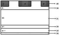
步骤S3:生长漂移层。如图10和图11所示,所述的漂移层包含nx第一漂移层31和n-第二漂移层30,所述的nx第一漂移层31和n-第二漂移层30为同质材料,具体包括:Step S3: growing a drift layer. As shown in FIG. 10 and FIG. 11 , the drift layer includes nx first drift layers 31 and n- second drift layers 30 , and the nx first drift layers 31 and n- second drift layers 30 are homogeneous materials, including:
a.如图10所示,通过物理或者化学气相沉积获得,具体为:利用化学气相沉积或物理气相沉积等方法将同质材料nx第一漂移层31生长到n+型缓冲层20之上,生长源为SiH4和C2H4,或者其他Si源和C源气体,掺杂源为NH3,生长温度为1500-1700℃。nx第一漂移层31自下而上形成了渐变掺杂结构,具体地,nx第一漂移层31自下而上掺杂浓度首先逐渐由低到高,其次逐渐由高到低。举例来说,nx第一漂移层31中间部分的高掺层浓度为1×1016cm-3~1×1017cm-3,厚度约占nx第一漂移层31总厚度的50%,nx第一漂移层31上下两侧部分的低掺层浓度为1×1015cm-3~1×1016cm-3,厚度分别约占nx第一漂移层31总厚度的25%。nx第一漂移层31的厚度占比整个漂移层的厚度为50-80%,举例来说nx第一漂移层31的厚度为5-8μm。a. As shown in FIG. 10, obtained by physical or chemical vapor deposition, specifically: using chemical vapor deposition or physical vapor deposition and other methods to grow the nx
b.如图11所示,通过物理或者化学气相沉积获得,具体为:利用化学气相沉积或物理气相沉积等方法将同质材料n-第二漂移层30生长到nx第一漂移层31之上,生长源为SiH4和C2H4,或者其他Si源和C源气体,掺杂源为NH3,生长温度为1500-1700℃。n-第二漂移层30的厚度占比整个漂移层的厚度为20-50%。b. As shown in FIG. 11, obtained by physical or chemical vapor deposition, specifically: using chemical vapor deposition or physical vapor deposition and other methods to grow the n-
最后,经过步骤S4-S6,完成一种兼具低导通压降和高可靠性的SiC肖特基器件的制备,如图11所示。Finally, through steps S4-S6, the preparation of a SiC Schottky device with both low on-voltage drop and high reliability is completed, as shown in FIG. 11 .
对比例1Comparative Example 1
对比例1与实施例1的差别在于,漂移层采用均一的掺杂浓度5×1015cm-3,厚度为10μm。The difference between Comparative Example 1 and Example 1 is that the drift layer adopts a uniform doping concentration of 5×1015 cm−3 and a thickness of 10 μm.
参考图12,可见当采用实施例1的nx第一漂移层结构,即中间部分1×1016cm-3和两侧5×1015cm-3变掺杂结构,导通电流得到显著提升,同时反向阻断时,在主结PN处发生较高的碰撞电离可能性,而靠近n+型缓冲层20一侧的碰撞电离可能性明显降低,从而减小了缓冲层一侧材料缺陷扩展的可能性,提高了器件的长期稳定性。Referring to FIG. 12 , it can be seen that when the nx first drift layer structure of Example 1 is adopted, that is, the 1×1016 cm-3 in the middle part and the 5×1015 cm-3 variable doping structure on both sides, the on-current is significantly improved, At the same time, when reverse blocking occurs, a higher probability of impact ionization occurs at the main junction PN, while the probability of impact ionization on the side close to the n+-
上述实施例仅用来进一步说明本发明的一种具有低导通压降的SiC基肖特基器件及其制备方法,但本发明并不局限于实施例,凡是依据本发明的技术实质对以上实施例所作的任何简单修改、等同变化与修饰,均落入本发明技术方案的保护范围内。The above embodiments are only used to further illustrate a SiC-based Schottky device with low on-voltage drop and a preparation method thereof of the present invention, but the present invention is not limited to the embodiments, and the technical essence of the present invention is consistent with the above. Any simple modifications, equivalent changes and modifications made in the embodiments fall within the protection scope of the technical solutions of the present invention.
Claims (10)
Translated fromChinesePriority Applications (1)
| Application Number | Priority Date | Filing Date | Title |
|---|---|---|---|
| CN202210532495.7ACN115117146B (en) | 2022-05-12 | 2022-05-12 | A SiC-based Schottky device with low on-state voltage drop and a method for preparing the same |
Applications Claiming Priority (1)
| Application Number | Priority Date | Filing Date | Title |
|---|---|---|---|
| CN202210532495.7ACN115117146B (en) | 2022-05-12 | 2022-05-12 | A SiC-based Schottky device with low on-state voltage drop and a method for preparing the same |
Publications (2)
| Publication Number | Publication Date |
|---|---|
| CN115117146Atrue CN115117146A (en) | 2022-09-27 |
| CN115117146B CN115117146B (en) | 2025-05-16 |
Family
ID=83325656
Family Applications (1)
| Application Number | Title | Priority Date | Filing Date |
|---|---|---|---|
| CN202210532495.7AActiveCN115117146B (en) | 2022-05-12 | 2022-05-12 | A SiC-based Schottky device with low on-state voltage drop and a method for preparing the same |
Country Status (1)
| Country | Link |
|---|---|
| CN (1) | CN115117146B (en) |
Cited By (1)
| Publication number | Priority date | Publication date | Assignee | Title |
|---|---|---|---|---|
| CN120400988A (en)* | 2025-07-03 | 2025-08-01 | 江苏鑫华半导体科技股份有限公司 | Silicon carbide epitaxial wafer, preparation method thereof, and semiconductor device |
Citations (7)
| Publication number | Priority date | Publication date | Assignee | Title |
|---|---|---|---|---|
| JP2006210569A (en)* | 2005-01-27 | 2006-08-10 | Shindengen Electric Mfg Co Ltd | Semiconductor device and manufacturing method thereof |
| JP2010040562A (en)* | 2008-07-31 | 2010-02-18 | Mitsubishi Electric Corp | Semiconductor device, and manufacturing method thereof |
| CN102376777A (en)* | 2010-08-24 | 2012-03-14 | 上海芯石微电子有限公司 | Junction barrier schottky having low forward voltage drop |
| WO2013153909A1 (en)* | 2012-04-12 | 2013-10-17 | 富士電機株式会社 | Wide band gap semiconductor device and manufacturing method therefor |
| CN103890920A (en)* | 2011-11-15 | 2014-06-25 | 富士电机株式会社 | Semiconductor device and method for manufacturing semiconductor device |
| US20140266403A1 (en)* | 2013-03-15 | 2014-09-18 | Cree, Inc. | Low Loss Electronic Devices Having Increased Doping for Reduced Resistance and Methods of Forming the Same |
| US20150001667A1 (en)* | 2012-07-03 | 2015-01-01 | Shindengen Electric Manufacturing Co., Ltd. | Semiconductor device |
- 2022
- 2022-05-12CNCN202210532495.7Apatent/CN115117146B/enactiveActive
Patent Citations (7)
| Publication number | Priority date | Publication date | Assignee | Title |
|---|---|---|---|---|
| JP2006210569A (en)* | 2005-01-27 | 2006-08-10 | Shindengen Electric Mfg Co Ltd | Semiconductor device and manufacturing method thereof |
| JP2010040562A (en)* | 2008-07-31 | 2010-02-18 | Mitsubishi Electric Corp | Semiconductor device, and manufacturing method thereof |
| CN102376777A (en)* | 2010-08-24 | 2012-03-14 | 上海芯石微电子有限公司 | Junction barrier schottky having low forward voltage drop |
| CN103890920A (en)* | 2011-11-15 | 2014-06-25 | 富士电机株式会社 | Semiconductor device and method for manufacturing semiconductor device |
| WO2013153909A1 (en)* | 2012-04-12 | 2013-10-17 | 富士電機株式会社 | Wide band gap semiconductor device and manufacturing method therefor |
| US20150001667A1 (en)* | 2012-07-03 | 2015-01-01 | Shindengen Electric Manufacturing Co., Ltd. | Semiconductor device |
| US20140266403A1 (en)* | 2013-03-15 | 2014-09-18 | Cree, Inc. | Low Loss Electronic Devices Having Increased Doping for Reduced Resistance and Methods of Forming the Same |
Cited By (1)
| Publication number | Priority date | Publication date | Assignee | Title |
|---|---|---|---|---|
| CN120400988A (en)* | 2025-07-03 | 2025-08-01 | 江苏鑫华半导体科技股份有限公司 | Silicon carbide epitaxial wafer, preparation method thereof, and semiconductor device |
Also Published As
| Publication number | Publication date |
|---|---|
| CN115117146B (en) | 2025-05-16 |
Similar Documents
| Publication | Publication Date | Title |
|---|---|---|
| CN114823911B (en) | Trench silicon carbide MOSFET with integrated high-speed freewheeling diode and preparation method thereof | |
| CN108417617B (en) | Silicon carbide trench MOSFETs and method of making the same | |
| CN105720110A (en) | SiC annular floating-point type P+ structured junction barrier Schottky diode and preparation method thereof | |
| CN116581151B (en) | A low turn-on voltage gallium oxide Schottky diode and its preparation method | |
| CN102376779B (en) | SiC Schottky diode and its manufacturing method | |
| CN101315887A (en) | Ohmic contact fabrication method for semi-insulating SiC semiconductor device | |
| CN112038412A (en) | Silicon carbide-based DSRD device with p-type variable doping base region and preparation method thereof | |
| CN116487445A (en) | A silicon carbide power device surrounding a P+ gradient ring with an N- region and its preparation method | |
| CN118448463A (en) | A diamond trench gate VDMOS device and its preparation method | |
| CN112018177A (en) | Full-vertical Si-based GaN UMOSFET power device and preparation method thereof | |
| CN107452624A (en) | Schottky contacts SiC IGBT and preparation method thereof | |
| CN115117146A (en) | SiC-based schottky device with low conduction voltage drop and preparation method thereof | |
| CN112951905B (en) | A SiC reverse conduction insulated gate bipolar transistor device and its manufacturing method | |
| CN106024627A (en) | Manufacturing method of SiC-based super-junction IGBT (Insulated Gate Bipolar Transistor) with low off-state loss | |
| CN118610274A (en) | Thick insulating layer pin junction terminal gallium oxide Schottky barrier diode and preparation method thereof | |
| CN118610260A (en) | p-NiO/n-Ga2O3 hole super-injection low resistance vertical field effect transistor and preparation method thereof | |
| CN106611798A (en) | N type silicon carbide semiconductor Schottky diode structure | |
| CN209963064U (en) | SiC-based DMOSFET device | |
| CN116417520B (en) | A gallium oxide field effect transistor and its preparation method | |
| CN116153982A (en) | Diamond drift step diode with field plate termination structure and preparation method | |
| CN115117145B (en) | SiC-based MOSFET device with low on-resistance and preparation method thereof | |
| CN114843365A (en) | A lateral structure 4H-silicon carbide/β-gallium oxide heterojunction high temperature solar blind detector and preparation method thereof | |
| CN112038411A (en) | Vertical aluminum nitride PN junction diode based on silicon carbide substrate and preparation method | |
| CN220189658U (en) | Silicon carbide Schottky diode structure | |
| CN111799336A (en) | A kind of SiC MPS diode device and preparation method thereof |
Legal Events
| Date | Code | Title | Description |
|---|---|---|---|
| PB01 | Publication | ||
| PB01 | Publication | ||
| SE01 | Entry into force of request for substantive examination | ||
| SE01 | Entry into force of request for substantive examination | ||
| GR01 | Patent grant | ||
| GR01 | Patent grant |