CN115083486A - TLC data programming with hybrid parity - Google Patents
TLC data programming with hybrid parityDownload PDFInfo
- Publication number
- CN115083486A CN115083486ACN202110665754.9ACN202110665754ACN115083486ACN 115083486 ACN115083486 ACN 115083486ACN 202110665754 ACN202110665754 ACN 202110665754ACN 115083486 ACN115083486 ACN 115083486A
- Authority
- CN
- China
- Prior art keywords
- data
- memory
- xor
- parity
- storage device
- Prior art date
- Legal status (The legal status is an assumption and is not a legal conclusion. Google has not performed a legal analysis and makes no representation as to the accuracy of the status listed.)
- Pending
Links
Images


Classifications
- G—PHYSICS
- G06—COMPUTING OR CALCULATING; COUNTING
- G06F—ELECTRIC DIGITAL DATA PROCESSING
- G06F3/00—Input arrangements for transferring data to be processed into a form capable of being handled by the computer; Output arrangements for transferring data from processing unit to output unit, e.g. interface arrangements
- G06F3/06—Digital input from, or digital output to, record carriers, e.g. RAID, emulated record carriers or networked record carriers
- G06F3/0601—Interfaces specially adapted for storage systems
- G06F3/0628—Interfaces specially adapted for storage systems making use of a particular technique
- G06F3/0638—Organizing or formatting or addressing of data
- G06F3/064—Management of blocks
- G—PHYSICS
- G06—COMPUTING OR CALCULATING; COUNTING
- G06F—ELECTRIC DIGITAL DATA PROCESSING
- G06F11/00—Error detection; Error correction; Monitoring
- G06F11/07—Responding to the occurrence of a fault, e.g. fault tolerance
- G06F11/08—Error detection or correction by redundancy in data representation, e.g. by using checking codes
- G06F11/10—Adding special bits or symbols to the coded information, e.g. parity check, casting out 9's or 11's
- G06F11/1076—Parity data used in redundant arrays of independent storages, e.g. in RAID systems
- G06F11/108—Parity data distribution in semiconductor storages, e.g. in SSD
- G—PHYSICS
- G11—INFORMATION STORAGE
- G11C—STATIC STORES
- G11C16/00—Erasable programmable read-only memories
- G11C16/02—Erasable programmable read-only memories electrically programmable
- G11C16/06—Auxiliary circuits, e.g. for writing into memory
- G11C16/10—Programming or data input circuits
- G—PHYSICS
- G06—COMPUTING OR CALCULATING; COUNTING
- G06F—ELECTRIC DIGITAL DATA PROCESSING
- G06F11/00—Error detection; Error correction; Monitoring
- G06F11/07—Responding to the occurrence of a fault, e.g. fault tolerance
- G06F11/08—Error detection or correction by redundancy in data representation, e.g. by using checking codes
- G06F11/10—Adding special bits or symbols to the coded information, e.g. parity check, casting out 9's or 11's
- G06F11/1004—Adding special bits or symbols to the coded information, e.g. parity check, casting out 9's or 11's to protect a block of data words, e.g. CRC or checksum
- G—PHYSICS
- G06—COMPUTING OR CALCULATING; COUNTING
- G06F—ELECTRIC DIGITAL DATA PROCESSING
- G06F11/00—Error detection; Error correction; Monitoring
- G06F11/07—Responding to the occurrence of a fault, e.g. fault tolerance
- G06F11/08—Error detection or correction by redundancy in data representation, e.g. by using checking codes
- G06F11/10—Adding special bits or symbols to the coded information, e.g. parity check, casting out 9's or 11's
- G06F11/1008—Adding special bits or symbols to the coded information, e.g. parity check, casting out 9's or 11's in individual solid state devices
- G06F11/1068—Adding special bits or symbols to the coded information, e.g. parity check, casting out 9's or 11's in individual solid state devices in sector programmable memories, e.g. flash disk
- G—PHYSICS
- G06—COMPUTING OR CALCULATING; COUNTING
- G06F—ELECTRIC DIGITAL DATA PROCESSING
- G06F3/00—Input arrangements for transferring data to be processed into a form capable of being handled by the computer; Output arrangements for transferring data from processing unit to output unit, e.g. interface arrangements
- G06F3/06—Digital input from, or digital output to, record carriers, e.g. RAID, emulated record carriers or networked record carriers
- G06F3/0601—Interfaces specially adapted for storage systems
- G06F3/0602—Interfaces specially adapted for storage systems specifically adapted to achieve a particular effect
- G06F3/0626—Reducing size or complexity of storage systems
- G—PHYSICS
- G06—COMPUTING OR CALCULATING; COUNTING
- G06F—ELECTRIC DIGITAL DATA PROCESSING
- G06F3/00—Input arrangements for transferring data to be processed into a form capable of being handled by the computer; Output arrangements for transferring data from processing unit to output unit, e.g. interface arrangements
- G06F3/06—Digital input from, or digital output to, record carriers, e.g. RAID, emulated record carriers or networked record carriers
- G06F3/0601—Interfaces specially adapted for storage systems
- G06F3/0668—Interfaces specially adapted for storage systems adopting a particular infrastructure
- G06F3/0671—In-line storage system
- G06F3/0673—Single storage device
- G—PHYSICS
- G11—INFORMATION STORAGE
- G11C—STATIC STORES
- G11C29/00—Checking stores for correct operation ; Subsequent repair; Testing stores during standby or offline operation
- G11C29/04—Detection or location of defective memory elements, e.g. cell constructio details, timing of test signals
- G11C29/08—Functional testing, e.g. testing during refresh, power-on self testing [POST] or distributed testing
- G11C29/12—Built-in arrangements for testing, e.g. built-in self testing [BIST] or interconnection details
- G11C29/38—Response verification devices
- G11C29/42—Response verification devices using error correcting codes [ECC] or parity check
Landscapes
- Engineering & Computer Science (AREA)
- Theoretical Computer Science (AREA)
- General Engineering & Computer Science (AREA)
- Physics & Mathematics (AREA)
- General Physics & Mathematics (AREA)
- Human Computer Interaction (AREA)
- Quality & Reliability (AREA)
- Computer Security & Cryptography (AREA)
- Techniques For Improving Reliability Of Storages (AREA)
Abstract
Translated fromChinese
Description
Translated fromChinese背景技术Background technique
技术领域technical field
本公开的实施方案整体涉及改进对数据存储设备诸如固态驱动器(SSD)的编程。Embodiments of the present disclosure relate generally to improving programming of data storage devices such as solid state drives (SSDs).
相关领域的描述Description of related fields
编程或写入数据可能需要两个写入阶段:模糊和精细。在模糊-精细编程中,要写入的位不能仅写入一次。相反,数据需要首先通过模糊编程写入,在模糊编程中提供电压脉冲以将当前状态推送到解析度较高状态,但并非完全解析状态。精细编程在模糊编程之后的一个时间点执行,以在完全解析状态下再次写入数据。Programming or writing data may require two phases of writing: fuzzy and fine. In fuzzy-fine programming, the bit to be written cannot be written only once. Instead, the data needs to be written first through fuzzy programming, where voltage pulses are provided to push the current state to a higher-resolution state, but not a fully-resolved state. Fine programming is performed at a point in time after fuzzy programming to write data again in a fully resolved state.
在将数据编程或写入到数据存储设备的相应位置时,可能会累积编程失败,诸如位误差。为了修复编程失败,由误差校正引擎(诸如奇偶引擎或低密度奇偶校验(LDPC)引擎)生成异或(XOR)奇偶数据。XOR奇偶数据存储在数据写入的每个位置中。例如,如果将数据精细编程到第一非易失性存储器设备,则首先将数据编程到易失性存储器设备高速缓存或第二非易失性存储器设备高速缓存。然后将数据模糊编程到第一非易失性存储器设备。在完成对第一非易失性存储器设备的模糊编程之后,将数据精细编程到第一非易失性存储器设备。XOR奇偶数据可以与编程数据一起生成并存储在数据编程序列的每个位置中,诸如易失性存储器设备高速缓存、第二非易失性存储器设备高速缓存、对第一非易失性存储器设备的模糊编程以及对第一非易失性存储器设备的精细编程中。XOR奇偶数据在先前提及的每个存储器设备中的累积增加了XOR奇偶开销,并且减少了数据存储设备中用户数据的过度供应或容量。Program failures, such as bit errors, may accumulate when data is programmed or written to the corresponding locations of the data storage device. To repair programming failures, exclusive-or (XOR) parity data is generated by an error correction engine, such as a parity engine or a low density parity check (LDPC) engine. XOR parity data is stored in each location where data is written. For example, if data is finely programmed to a first non-volatile memory device, the data is first programmed to the volatile memory device cache or the second non-volatile memory device cache. The data is then fuzzy programmed to the first non-volatile memory device. After the fuzzy programming of the first non-volatile memory device is completed, data is finely programmed to the first non-volatile memory device. XOR parity data can be generated along with the programming data and stored in each location of the data programming sequence, such as a volatile memory device cache, a second non-volatile memory device cache, a cache for the first non-volatile memory device of fuzzy programming and fine-grained programming of the first non-volatile memory device. The accumulation of XOR parity data in each of the previously mentioned memory devices increases the XOR parity overhead and reduces the over-provisioning or capacity of user data in the data storage device.
因此,本领域需要改进对非易失性存储器的编程,同时减小XOR奇偶开销并保持或增加数据存储设备的可靠性。Accordingly, there is a need in the art to improve programming of non-volatile memory while reducing XOR parity overhead and maintaining or increasing the reliability of data storage devices.
发明内容SUMMARY OF THE INVENTION
本公开整体涉及改进对数据存储设备诸如固态驱动器(SSD)的编程。第一存储器设备具有第一XOR元素,并且第二存储器设备具有第二XOR元素。该第一XOR元素与该第一存储器设备的容量的比率基本上小于该第二XOR元素与该第二存储器设备的容量的比率。用于发现编程失败的读取验证操作在字线与字线的基础上、在擦除块与擦除块的基础上或者在字线与字线的基础和擦除块与擦除块的基础两者上执行。因为这些编程失败在对该第二存储器设备编程之前被发现并修复,所以该第二XOR元素可显著地减小。The present disclosure generally relates to improving programming of data storage devices such as solid state drives (SSDs). The first memory device has a first XOR element and the second memory device has a second XOR element. The ratio of the first XOR element to the capacity of the first memory device is substantially smaller than the ratio of the second XOR element to the capacity of the second memory device. Read verify operations for finding program failures on a wordline-to-wordline basis, an eraseblock-to-eraseblock basis, or a wordline-to-wordline basis and an eraseblock-to-eraseblock basis performed on both. Because these programming failures are discovered and repaired prior to programming the second memory device, the second XOR element can be significantly reduced.
在一个实施方案中,数据存储设备包括控制器和耦接到该控制器的存储器设备。存储器设备包括具有第一存储大小的第一奇偶部分的第一超级块和具有第二存储大小的第二奇偶部分的第二超级块。所述第一存储尺寸小于所述第二存储尺寸。In one embodiment, a data storage device includes a controller and a memory device coupled to the controller. The memory device includes a first superblock having a first parity portion of a first storage size and a second superblock having a second parity portion of a second storage size. The first storage size is smaller than the second storage size.
在另一个实施方案中,数据存储设备包括存储器设备以及耦接到存储器设备的控制器。所述控制器被配置为:从主机设备接收主机数据;为所述主机数据生成第一异或(XOR)奇偶数据;用编码器对所述主机数据和所述第一XOR奇偶数据进行编码;将所述主机数据和所述第一XOR奇偶数据写入到第一存储器超级块;对写入到所述第一存储器超级块的有效数据和第一XOR奇偶数据进行解码,其中所述有效数据与尚未被位于所述第一存储器超级块中的所述主机设备修改的所述主机数据相对应;为所述解码的有效数据生成第二XOR奇偶数据;用所述编码器对所述解码的数据和第二XOR奇偶数据进行重新编码;以及将所述重新编码的数据和奇偶数据写入到第二存储器超级块。所述重新编码的第二XOR奇偶数据的大小小于所述第一XOR奇偶数据的所述大小。In another embodiment, a data storage device includes a memory device and a controller coupled to the memory device. The controller is configured to: receive host data from a host device; generate first exclusive-OR (XOR) parity data for the host data; encode the host data and the first XOR parity data with an encoder; writing the host data and the first XOR parity data to a first memory superblock; decoding the valid data and first XOR parity data written to the first memory superblock, wherein the valid data corresponding to the host data that has not been modified by the host device located in the first memory superblock; generating second XOR parity data for the decoded valid data; re-encoding the data and the second XOR parity data; and writing the re-encoded data and parity data to a second memory superblock. The size of the recoded second XOR parity data is smaller than the size of the first XOR parity data.
在另一个实施方案中,数据存储设备包括:存储器装置,所述存储器装置包括第一存储器超级块和第二存储器超级块;用于将主机数据和奇偶数据存储在所述第一存储器超级块中的装置;以及用于将所述主机数据和奇偶数据的副本存储在所述第二存储器超级块中的装置,其中,与所述第一超级块中的奇偶数据存储量相比,所述奇偶数据的所述副本利用所述第二超级块中较少的奇偶数据存储量。In another embodiment, a data storage device includes: a memory device comprising a first memory superblock and a second memory superblock; for storing host data and parity data in the first memory superblock and means for storing a copy of the host data and parity data in the second memory superblock, wherein the parity is compared to the amount of parity data stored in the first superblock The copy of data utilizes less parity data storage in the second superblock.
附图说明Description of drawings
因此,通过参考实施方案,可以获得详细理解本公开的上述特征的方式、本公开的更具体描述、上述简要概述,所述实施方案中的一些在附图中示出。然而,应当注意的是,附图仅示出了本公开的典型实施方案并且因此不应视为限制其范围,因为本公开可以允许其他同等有效的实施方案。Thus, a detailed understanding of the manner in which the above-described features of the disclosure, a more detailed description of the disclosure, and the foregoing brief summary can be obtained by reference to the embodiments, some of which are illustrated in the accompanying drawings. It is to be noted, however, that the appended drawings illustrate only typical embodiments of this disclosure and are therefore not to be considered limiting of its scope, for the disclosure may admit to other equally effective embodiments.
图1是示出根据所公开的实施方案的存储系统的示意性框图,其中数据存储设备可以用作主机设备的存储设备。1 is a schematic block diagram illustrating a storage system in which a data storage device may function as a storage device for a host device, according to disclosed embodiments.
图2A和图2B是根据所公开的实施方案的调度模糊-精细编程的示意图。2A and 2B are schematic diagrams of scheduling fuzzy-fine programming in accordance with the disclosed embodiments.
图3是根据所公开的实施方案的具有超级块的完全管芯冗余的水平异或(XOR)方案的示意图。3 is a schematic diagram of a horizontal exclusive-OR (XOR) scheme with full die redundancy with superblocks in accordance with the disclosed embodiments.
图4是根据所公开的实施方案的多级单元中的异或(XOR)的可能选项的图示。4 is an illustration of possible options for exclusive-or (XOR) in a multi-level cell according to the disclosed embodiments.
图5A和图5B是根据所公开的实施方案的各种编程失败类型的图示。5A and 5B are illustrations of various types of programming failures in accordance with the disclosed embodiments.
图6A和图6B是根据所公开的实施方案的超级块的减少的水平异或(XOR)方案的示意图。6A and 6B are schematic diagrams of a reduced horizontal exclusive-or (XOR) scheme for superblocks, according to disclosed embodiments.
图7是根据所公开的实施方案的超级块的减少的水平异或(XOR)方案的示意图。7 is a schematic diagram of a reduced horizontal exclusive-OR (XOR) scheme for a superblock in accordance with the disclosed embodiments.
图8是根据所公开的实施方案的超级块的减少的竖直异或(XOR)方案的示意图。8 is a schematic diagram of a reduced vertical exclusive-OR (XOR) scheme of a superblock in accordance with the disclosed embodiments.
图9是示出根据所公开的实施方案的执行模糊-精细编程的方法的流程图。9 is a flowchart illustrating a method of performing fuzzy-fine programming in accordance with the disclosed embodiments.
为了有助于理解,在可能的情况下,使用相同的参考标号来表示附图中共有的相同元件。可以设想是,在一个实施方案中公开的元件可以有利地用于其他实施方案而无需具体叙述。To aid understanding, where possible, the same reference numerals have been used to refer to the same elements that are common to the figures. It is contemplated that elements disclosed in one embodiment may be used to advantage on other embodiments without specific recitation.
具体实施方式Detailed ways
在下文中,参考本公开的实施方案。然而,应当理解的是,本公开不限于具体描述的实施方案。相反,思考以下特征和元件的任何组合(无论是否与不同实施方案相关)以实现和实践本公开。此外,尽管本公开的实施方案可以实现优于其他可能解决方案和/或优于现有技术的优点,但是否通过给定实施方案来实现特定优点不是对本公开的限制。因此,以下方面、特征、实施方案和优点仅是说明性的,并且不被认为是所附权利要求书的要素或限制,除非在权利要求书中明确地叙述。同样地,对“本公开”的引用不应当被解释为本文公开的任何发明主题的概括,并且不应当被认为是所附权利要求书的要素或限制,除非在权利要求书中明确地叙述。In the following, reference is made to embodiments of the present disclosure. It should be understood, however, that the present disclosure is not limited to the specifically described embodiments. Rather, any combination of the following features and elements, whether related to different embodiments or not, is contemplated to implement and practice the present disclosure. Furthermore, although embodiments of the present disclosure may achieve advantages over other possible solutions and/or over the prior art, whether or not a particular advantage is achieved by a given embodiment is not a limitation of the present disclosure. Accordingly, the following aspects, features, embodiments, and advantages are merely illustrative, and are not to be considered elements or limitations of the appended claims unless expressly recited in the claims. Likewise, references to "the present disclosure" should not be construed as a generalization of any inventive subject matter disclosed herein, and should not be considered an element or limitation of the appended claims unless expressly recited in the claims.
本公开整体涉及改进对数据存储设备诸如固态驱动器(SSD)的编程。第一存储器设备具有第一XOR元素,并且第二存储器设备具有第二XOR元素。该第一XOR元素与该第一存储器设备的容量的比率基本上小于该第二XOR元素与该第二存储器设备的容量的比率。用于发现编程失败的读取验证操作在字线与字线的基础上、在擦除块与擦除块的基础上或者在字线与字线的基础和擦除块与擦除块的基础两者上执行。因为这些编程失败在对该第二存储器设备编程之前被发现并修复,所以该第二XOR元素可显著地减小。The present disclosure generally relates to improving programming of data storage devices such as solid state drives (SSDs). The first memory device has a first XOR element and the second memory device has a second XOR element. The ratio of the first XOR element to the capacity of the first memory device is substantially smaller than the ratio of the second XOR element to the capacity of the second memory device. Read verify operations for finding program failures on a wordline-to-wordline basis, an eraseblock-to-eraseblock basis, or a wordline-to-wordline basis and an eraseblock-to-eraseblock basis performed on both. Because these programming failures are discovered and repaired prior to programming the second memory device, the second XOR element can be significantly reduced.
图1是示出根据公开的实施方案的存储系统100的示意性框图,其中数据存储设备106可以用作主机设备104的存储设备。例如,主机设备104可以利用包括在数据存储设备106中的非易失性存储器(NVM)110来存储和检索数据。主机设备104包括主机DRAM 138。在一些示例中,存储系统100可以包括可作为存储阵列工作的多个存储设备,诸如数据存储设备106。例如,存储系统100可以包括多个数据存储设备106,其被配置成共同用作主机设备104的大容量存储设备的廉价/独立磁盘(RAID)冗余阵列。FIG. 1 is a schematic block diagram illustrating a
存储系统100包括主机设备104,该主机设备可以向一个或多个存储设备诸如数据存储设备106存储数据和/或从其检索数据。如图1所示,主机设备104可以经由接口114与数据存储设备106通信。主机设备104可以包括多种设备中的任何一种,包括计算机服务器、网络附接存储(NAS)单元、台式计算机、笔记本(即膝上型)计算机、平板计算机、机顶盒、电话手机诸如所谓的“智能”电话、所谓的“智能”平板电脑、电视、相机、显示设备、数字媒体播放器、视频游戏控制台、视频流设备、或能够从数据存储设备发送或接收数据的其它设备等。
数据存储设备106包括控制器108、NVM 110、电源111、易失性存储器112、接口114和写入缓冲区116。在一些示例中,为了清楚起见,数据存储设备106可以包括图1中未示出的附加部件。例如,数据存储设备106可以包括印刷电路板(PCB),数据存储设备106的部件机械地附接到该印刷电路板,并且该印刷电路板包括电互连数据存储设备106的部件等的导电迹线。在一些示例中,数据存储设备106的物理尺寸和连接器配置可以符合一个或多个标准形状因数。一些示例性标准形状因子包括但不限于3.5”数据存储设备(例如,HDD或SSD)、2.5”数据存储设备、1.8”数据存储设备、外围部件互连(PCI)、PCI扩展(PCI-X)、PCIExpress(PCIe)(例如,PCIe x1、x4、x8、x16、PCIe Mini卡、MiniPCI等)。在一些示例中,数据存储设备106可以直接耦接(例如,直接焊接)到主机设备104的母板。
数据存储设备106的接口114可以包括用于与主机设备104交换数据的数据总线和用于与主机设备104交换命令的控制总线中的一者或两者。接口114可以根据任何合适的协议操作。例如,接口114可以根据以下协议中的一个或多个协议来操作:高级技术附件(ATA)(例如,串行ATA(SATA)和并行ATA(PATA))、光纤信道协议(FCP)、小型计算机系统接口(SCSI)、串行附接SCSI(SAS)、PCI和PCIe、非易失性存储器express(NVMe)、OpenCAPI、GenZ、高速缓存相干接口加速器(CCIX)、开放信道SSD(OCSSD)等。接口114的电连接(例如,数据总线、控制总线或两者)电连接到控制器108,从而提供主机设备104与控制器108之间的电连接,允许在主机设备104与控制器108之间交换数据。在一些示例中,接口114的电连接还可以允许数据存储设备106从主机设备104接收电力。例如,如图1所示,电源111可以经由接口114从主机设备104接收电力。The
NVM 110可以包括多个存储器设备或存储器单元。NVM 110可以被配置成存储和/或检索数据。例如,NVM 110的存储单元可以接收数据并且从控制器108接收指示存储单元存储数据的消息。类似地,NVM 110的存储单元可以从控制器108接收指示存储单元检索数据的消息。在一些示例中,存储单元中的每个存储单元可以被称为管芯。在一些示例中,单个物理芯片可以包括多个管芯(即,多个存储单元)。在一些示例中,每个存储单元可以被配置成存储相对大量的数据(例如,128MB、256MB、512MB、1GB、2GB、4GB、8GB、16GB、32GB、64GB、128GB、256GB、512GB、1TB等)。NVM 110 may include multiple memory devices or memory cells. NVM 110 may be configured to store and/or retrieve data. For example, a storage unit of NVM 110 may receive data and a message from
在一些示例中,NVM 110的每个存储单元可以包括任何类型的非易失性存储器设备,诸如闪存存储器设备、相变存储器(PCM)设备、电阻随机存取存储器(ReRAM)设备、磁阻随机存取存储器(MRAM)设备、铁电随机存取存储器(F-RAM)、全息存储器设备、以及任何其它类型的非易失性存储器设备。In some examples, each memory cell of NVM 110 may include any type of non-volatile memory device, such as flash memory devices, phase change memory (PCM) devices, resistive random access memory (ReRAM) devices, magnetoresistive random access Access memory (MRAM) devices, ferroelectric random access memory (F-RAM), holographic memory devices, and any other type of non-volatile memory device.
NVM 110可以包括多个闪存存储器设备或存储单元。NVM闪存存储器设备可以包括基于NAND或NOR的闪存存储器设备,并且可以基于包含在用于每个闪存存储器单元的晶体管的浮栅中的电荷来存储数据。在NVM闪存存储器设备中,闪存存储器设备可被划分成多个管芯,其中多个管芯中的每个管芯包括多个块,这些块可被进一步划分成多个页面。特定存储器设备内的多个块中的每个块可以包括多个NVM单元。NVM单元的行可以使用字线来电连接以限定多个页面中的页面。多个页面中的每个页面中的相应单元可以电连接到相应位线。此外,NVM闪存存储器设备可以是2D或3D设备,并且可以是单级单元(SLC)、多级单元(MLC)、三级单元(TLC)或四级单元(QLC)。控制器108可能以页面等级向NVM闪存存储器设备写入数据以及从NVM闪存存储器设备读取数据,并且以块等级从NVM闪存存储器设备擦除数据。NVM 110 may include multiple flash memory devices or storage units. NVM flash memory devices may include NAND or NOR based flash memory devices and may store data based on charges contained in the floating gates of transistors for each flash memory cell. In an NVM flash memory device, the flash memory device may be divided into a plurality of dies, where each die of the plurality of dies includes a plurality of blocks, which may be further divided into a plurality of pages. Each of the plurality of blocks within a particular memory device may include a plurality of NVM units. Rows of NVM cells may be electrically connected using word lines to define pages of multiple pages. A corresponding cell in each of the plurality of pages may be electrically connected to a corresponding bit line. Furthermore, NVM flash memory devices may be 2D or 3D devices, and may be single-level cell (SLC), multi-level cell (MLC), triple-level cell (TLC), or quad-level cell (QLC). The
数据存储设备106包括电源111,其可以向数据存储设备106的一个或多个部件提供电力。当以标准模式操作时,电源111可以使用由外部设备诸如主机设备104提供的电力向一个或多个部件供电。例如,电源111可以使用经由接口114从主机设备104接收的电力向一个或多个部件供电。在一些示例中,电源111可以包括一个或多个电力存储部件,其被配置成当以关闭模式操作时向一个或多个部件供电,诸如在停止从外部设备接收电力的情况下。以这种方式,电源111可以用作机载备用电源。一个或多个电力存储部件的一些示例包括但不限于电容器、超级电容器、电池等。在一些示例中,可由一个或多个电力存储部件存储的电量可以是一个或多个电力存储部件的成本和/或尺寸(例如,面积/体积)的函数。换句话说,随着由一个或多个电力存储部件存储的电量增加,一个或多个电力存储部件的成本和/或尺寸也增加。
数据存储设备106还包括易失性存储器112,其可以由控制器108用来存储信息。易失性存储器112可以包括一个或多个易失性存储器设备。在一些示例中,控制器108可以使用易失性存储器112作为高速缓存。例如,控制器108可以将高速缓存的信息存储在易失性存储器112中,直到高速缓存的信息被写入非易失性存储器110。如图1所示,易失性存储器112可以消耗从电源111接收的电力。易失性存储器112的示例包括但不限于随机存取存储器(RAM)、动态随机存取存储器(DRAM)、静态RAM(SRAM)和同步动态RAM(SDRAM(例如,DDR1、DDR2、DDR3、DDR3L、LPDDR3、DDR4、LPDDR4等))。
数据存储设备106包括控制器108,其可以管理数据存储设备106的一个或多个操作。例如,控制器108可以管理从NVM 110读取数据和/或将数据写入该NVM 110。在一些实施方案中,当数据存储设备106从主机设备104接收写入命令时,控制器108可以发起数据存储命令以将数据存储到该NVM 110并且监测数据存储命令的进度。控制器108可以确定存储系统100的至少一个操作特性,并且将至少一个操作特性存储到该NVM 110。在一些实施方案中,当数据存储设备106从主机设备104接收到写入命令时,控制器108在将数据发送至NVM110之前将与写入命令相关联的数据暂时存储在内部存储器或写入缓冲区116中。The
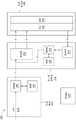
图2A是根据所公开的实施方案的调度模糊-精细编程的示意图。前端(FE)模块202包括第一XOR引擎204和第一静态随机存取存储器(SRAM)206。主机数据可最初递送到FE模块202。数据经过第一XOR引擎204并写入到第一SRAM 206。第一XOR引擎204在写入到SRAM206之前生成XOR奇偶信息。异或(XOR)奇偶信息用于提高用于存储数据的存储设备的可靠性,诸如使得能够对往返于NVM的数据写入失败或数据读取失败进行数据恢复,或者使得能够进行数据恢复以防电力丢失。存储设备可以是图1的数据存储设备106。可通过使用基于存储到存储设备的数据生成或计算的XOR奇偶信息来提供可靠性。第一XOR引擎204可以生成要写入到第一SRAM 206的第一奇偶流。第一SRAM 206可以包含数据可写入到的多个管芯。2A is a schematic diagram of scheduling fuzzy-fine programming in accordance with the disclosed embodiments. The front end (FE)
第二闪存管理器(FM2)模块210包括编码器212、第二SRAM 216、解码器214和第二XOR引擎232,其中第二XOR引擎232被配置为生成要写入到第二SRAM 216的第二奇偶流。解码器214可包括低档(LG)解码器和高档(HG)解码器。LG解码器可以实现低功率位翻转算法,诸如低密度奇偶校验(LDPC)算法。LG解码器可用于解码数据并校正位翻转,其中这种数据具有低误码率(BER)。HG解码器可以实现全功率解码和误差校正算法,这些算法可在LG解码器未能解码和校正数据中的位翻转时启动。HG解码器可用于在这种数据具有高BER的情况下校正位翻转。另选地,FM2可用组合的FE-FM单片替换。The second flash manager (FM2)
例如,编码器212和解码器214(包括LG解码器和HG解码器)可以包括处理电路或处理器(具有存储可由处理器执行的计算机可读程序代码(例如,固件)的计算机可读介质)、逻辑电路、专用集成电路(ASIC)、可编程逻辑控制器、嵌入式微控制器、它们的组合,等等。在一些示例中,编码器212和解码器214与存储控制器分开,并且在其它示例中,编码器212和解码器214嵌入在存储控制器中或是存储控制器的一部分。在一些示例中,LG解码器是硬化电路,诸如逻辑电路、ASIC等等。在一些示例中,HG解码器可以是软解码器(例如,由处理器实现)。数据可以在解码器214处解码之后写入到第二SRAM 216。第二SRAM 216处的数据可以进一步递送到编码器212,如以下所论述。For example,
存储器设备220可以是NAND存储器设备。存储器设备220可以包括TLC存储器222。应当理解,本文所论述的实施方案可不限于TLC存储器,并且可适用于任何多级单元存储器,诸如MLC存储器、QLC存储器等。SLC存储器、MLC存储器、TLC存储器、QLC存储器和PLC存储器根据存储器单元可以接受的位数来命名。例如,SLC存储器可以接受每个存储器单元一位,并且QLC存储器可以接受每个存储器单元四位。每个位在存储设备上寄存为1或0。
此外,TLC存储器222包括TLC异或(XOR)分区226,其中TLC XOR分区226存储奇偶数据或XOR数据。主机数据被写入到FE模块202的第一SRAM 206。当主机数据被写入到第一SRAM 206时,可以在FE模块202的第一XOR引擎204处同时生成第一XOR奇偶数据。主机数据和所生成的第一XOR奇偶数据从第一SRAM 206传递到编码器212以沿着流1进行编码。主机数据被编码并模糊写入到TLC存储器222。同样地,所生成的第一XOR奇偶数据被编码并且沿着流2模糊写入到存储器设备220的TLC XOR分区226。在模糊写入期间,控制器可以选择性地选取要读取的数据,以便允许将数据分类到相关的一个或多个流中。TLC存储器222可以是存储器设备220的专用于在电力损失事件的情况下保护数据的区域。Additionally, the
在流3处,在解码器214处从TLC存储器222读取主机数据。在解码器214处解码主机数据之后,主机数据沿着流4写入到FM2 210的第二SRAM 216,其中在FM2 210的第二XOR引擎232处进一步针对主机数据生成第二XOR奇偶数据。主机数据和第二XOR奇偶数据经过编码器212以沿着流5进行编码,并且沿着流6精细写入到TLC存储器222和TLC XOR分区226的相应位置。At stream 3, host data is read at decoder 214 from
图2B是根据所公开的实施方案的调度模糊-精细编程的示意图。TLC存储器222可进一步划分为第一TLC存储器分区222A和第二TLC存储器分区222B。第二TLC存储器分区222B可大于第一TLC存储器分区222A。此外,TLC XOR分区226可进一步划分为第一TLC XOR分区226A和第二TLC XOR分区226B。第二TLC XOR分区226B可小于第一TLC XOR分区226B。在一个实施方案中,第二TLC XOR分区226B的大小小于第一TLX XOR分区226A的大小,差异范围约50%。又如,第二TLC XOR分区226B的大小小于第一TLX XOR分区226A的大小,差异范围约50%。2B is a schematic diagram of scheduling fuzzy-fine programming in accordance with the disclosed embodiments. The
在一些示例中,第二TLC XOR分区226B的大小能够配置,使得控制器108可以根据诸如阈值、TLC存储器222健康状况(诸如TLC存储器的失败位计数(FBC))等因素,在数据存储设备106的寿命期间确定第二TLC XOR分区226B的大小。第一TLC存储器分区222A和第一TLC XOR分区226A可以是第一TLC超级块,并且第二TLC存储器分区222B和第二TLC XOR分区226B可以是第二超级块。In some examples, the size of the second
当模糊编程到TLC存储器222时,主机数据被编程到第一TLC XOR分区222A。同样,XOR奇偶数据被编程到第一TLC XOR分区226A。第一TLC存储器分区222A和第一TLC XOR分区226A可被认为是“主机写入”区域,其中在“主机写入”区域中编程的数据可能丢失或损坏。然而,当精细编程到TLC存储器222时,主机数据从第一TLC XOR分区222A被复制(即,回收副本),这仍然有效(即,尚未被另一主机命令重新写入或修剪),被重新编码并编程到第二TLC存储器分区222B,并且XOR奇偶数据被编程到第二TLC XOR分区226B。在精细编程到第二TLC存储器分区222B和第二TLC XOR分区226B之后,当数据的第一副本存储在第一TLC存储器分区222A中时,数据和XOR奇偶数据受到保护。出于上述原因,第二TLC存储器分区222B和第二TLC XOR分区226B可被认为是“回收副本”区域。When fuzzy programming to
由于精细编程可以利用减小的XOR奇偶方案,诸如下面描述的方案,因此可以减小所需XOR奇偶分区大小。例如,XOR奇偶数据减少约50%可以在7680GB SSD中释放约100GB的容量。然后,可利用释放的100GB容量来存储附加的主机数据。因此,可以减少存储器对XOR奇偶数据的过度供应,并且可以利用将用于存储XOR奇偶数据的存储器来存储主机数据或类似数据。Since fine programming can utilize a reduced XOR parity scheme, such as the one described below, the required XOR parity partition size can be reduced. For example, a ~50% reduction in XOR parity data can free up ~100GB of capacity in a 7680GB SSD. The freed 100GB can then be used to store additional host data. Therefore, over-provisioning of memory for XOR parity data can be reduced, and memory that will be used to store XOR parity data can be utilized to store host data or the like.
图3是根据所公开的实施方案的具有超级块300的完全管芯冗余的水平异或(XOR)方案的示意图。超级块300包括多个管芯(例如,管芯0-管芯7)和多条字线(WL)(例如,WL 0-WL 95)。所列出的管芯和字线的数量并非旨在进行限制,而是被示出以例示可能的实施方案。例如,超级块可以包括约32个管芯和多于或少于约96个WL。多个管芯中的每个管芯包括由PL0指示的第一平面和由PL1指示的第二平面。此外,多条字线中的每条字线包括四个串(STR)。每条字线的串的数量是基于超级块的存储器单元的类型。例如,QLC存储器包括每条字线四个串,TLC存储器包括每条字线三个串,并且SLC存储器包括每条字线一个串。3 is a schematic diagram of a horizontal exclusive-OR (XOR) scheme with full die redundancy of the
超级块300可以是区名称空间架构的示例,该区名称空间架构包括用于数据的七个管芯和用于XOR奇偶数据的第八管芯。超级块300的管芯7与XOR奇偶数据302相关联。因为管芯7仅包括XOR奇偶数据302,所以XOR奇偶数据302可以恢复另一个失效管芯304,诸如管芯1,其中恢复另一个失效管芯304包括恢复失效管芯的全部数据(即,完全管芯冗余)。此外,因为每个串诸如WL 0的串2横跨八个管芯中的每个管芯,所以每个串包括16个平面。因为管芯7包括XOR奇偶数据302,所以奇偶群组比为约1:7,其中XOR奇偶数据开销为约12.5%(即,1/8)。所列出的值并非旨在进行限制,而是提供可能实施方案的示例。
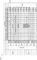
图4是根据所公开的实施方案的多级单元中的异或(XOR)的可能选项的图示。不可校正的误差校正码(UECC)数据误差的源包括编程状态失败(PSF)、静默编程失败和与磨损和数据保持相关的随机失败。PSF和静默编程失败可以与位失败比(BFR)和/或编程擦除(PE)循环相关联。磨损和DR相关的随机失败可以与扇区失败比(SFR)相关联。4 is an illustration of possible options for exclusive-or (XOR) in a multi-level cell according to the disclosed embodiments. Sources of uncorrectable error correction code (UECC) data errors include program state failures (PSFs), silent program failures, and random failures related to wear and data retention. PSF and silent program failures can be associated with bit fail ratios (BFRs) and/or program erase (PE) cycles. Wear and DR-related random failures can be associated with a sector failure ratio (SFR).
“XOR奇偶”列示出了每个实施方案中包括的XOR奇偶的类型。例如,完全管芯冗余(FDR)可以恢复整个失效管芯。然而,与FDR相关联的XOR奇偶数据可能需要超级块中的大量存储空间,从而减少了可以存储在超级块中的数据量。XOR奇偶数据或用于多个误差校正码(ECC)码字的任何其它奇偶方案诸如低密度奇偶校验(LDPC)可以用于恢复失败的数据位。例如,当失败位计数(FBC)大于阈值时,控制器诸如图1的控制器108可以利用XOR奇偶数据来恢复失败位,使得与失败位相关联的数据不包括失败位。The "XOR parity" column shows the type of XOR parity included in each implementation. For example, full die redundancy (FDR) can recover an entire failed die. However, XOR parity data associated with FDR may require a large amount of storage space in the superblock, reducing the amount of data that can be stored in the superblock. XOR parity data or any other parity scheme for multiple Error Correcting Code (ECC) codewords such as Low Density Parity Check (LDPC) can be used to recover failed data bits. For example, when the Failed Bit Count (FBC) is greater than a threshold, a controller such as
数据误差的另一个示例是编程失败,其中编程失败尺寸从一个WL-串-平面到2-擦除块失败两个平面而变化。与FBC误差不同,在XOR奇偶数据和LDPC两者可以用于校正FBC误差的情况下,XOR奇偶数据和类似奇偶方案可以用于校正编程失败。可以通过在超级块的不同位置中写入数据来修复编程失败,诸如PSF。例如,当单元具有不可接受的误码率(UBER)时,控制器可以避免将数据编程到具有UBER的单元。然而,静默编程失败可能无法被控制器检测到,并且不被觉察地被传递到NVM,诸如图1的NVM 110。静默编程失败可能导致降低数据存储设备诸如图1的数据存储设备106的可靠性的双重误差、三重误差或更高误差。Another example of a data error is a program failure, where the program failure size varies from one WL-string-plane to 2-erase block failure two planes. Unlike FBC errors, where both XOR parity data and LDPC can be used to correct FBC errors, XOR parity data and similar parity schemes can be used to correct for program failures. Program failures, such as PSFs, can be repaired by writing data in different locations of the superblock. For example, when the cell has an unacceptable bit error rate (UBER), the controller can avoid programming data to the cell with the UBER. However, silent programming failures may go undetected by the controller and pass unnoticed to an NVM, such as NVM 110 of FIG. 1 . Silent programming failures may result in double errors, triple errors, or higher errors that reduce the reliability of a data storage device such as
为了保护用户数据免于由于编程失败所致的失败,XOR奇偶数据方案需要足够大(即,低XOR奇偶比)以防止先前描述的编程失败和未描述但设想的任何编程失败的任何组合,并且也具有正确的几何结构。然而,XOR奇偶数据方案尺寸具有局限性。例如,通过增大XOR奇偶数据方案的尺寸,更少用户数据或任何其它数据可以存储在NVM中,原因是XOR奇偶数据占用NVM中的更多内存,其中更多内存可以用来存储更多用户数据。To protect user data from failures due to program failures, the XOR parity data scheme needs to be large enough (ie, a low XOR parity ratio) to prevent any combination of previously described program failures and any program failures not described but envisaged, and Also has the correct geometry. However, the XOR parity data scheme size has limitations. For example, by increasing the size of the XOR parity data scheme, less user data or any other data can be stored in the NVM because the XOR parity data occupies more memory in the NVM, where more memory can be used to store more users data.
“额外措施”列是指数据在高速缓存或缓冲器中的临时存储或者用于校验和修复误差的读取验证/增强后写入读取(EPWR)的等级。例如,缓冲器或高速缓存可以存储写入到超级块的数据的至多最后两条字线(2WL深度)。当将另一条字线写入到超级块时,存储在缓冲器或高速缓存中的最后两条字线中最旧的字线被释放,使得释放字线是指擦除数据。此外,读取验证/EPWR等级是指读取验证/EPWR操作的频率。例如,字线的读取验证/EPWR等级表示在字线被编程之后,发生读取验证/EPWR操作。The "Extra Measures" column refers to the temporary storage of data in a cache or buffer or the level of Read Verification/Enhanced Post Write Read (EPWR) for checksum repair errors. For example, a buffer or cache may store at most the last two word lines (2WL depth) of data written to the super block. When another word line is written to the super block, the oldest of the last two word lines stored in the buffer or cache is released, so that releasing the word line means erasing the data. Furthermore, the read verify/EPWR level refers to the frequency of read verify/EPWR operations. For example, a read verify/EPWR level for a word line indicates that a read verify/EPWR operation occurs after the word line is programmed.
如图4所示,每当存在附加固件(FW)读取验证/EPWR校验时,XOR奇偶比减小。例如,在第一FW读取验证/EPWR校验实施方案404处,在将数据从第一TLC存储器分区诸如图2B的第一TLC存储器222A复制到第二TLC存储器诸如图2B的第二TLC存储器222B的情况下,XOR奇偶比为约1:127。作为比较,无额外校验实施方案402所具有的XOR奇偶比为约1:63。第一FW读取验证/EPWR校验实施方案404包括字线的读取验证/EPWR等级。此外,高速缓存或缓冲器存储写入到超级块的数据的最后两条字线(例如,2WL深度)。通过进一步执行读取验证/EPWR校验,诸如第四FW读取验证/EPWR校验实施方案406,XOR奇偶比可以基本上减小到约0,其中缓冲器或高速缓存存储写入到超级块的最后擦除块,并且读取验证/EPWR操作在每当字线、擦除块或字线和擦除块两者被编程之后发生。As shown in Figure 4, the XOR parity decreases whenever there is an additional firmware (FW) read verification/EPWR check. For example, at the first FW read verify/EPWR verify
如果不需要校正PSF,则可以减少XOR奇偶数据比以及开销。例如,如果数据(诸如写入的至多最后两条字线或编程的最后擦除块)在源块(诸如SLC存储器、缓冲器和/或高速缓存)中仍可用,则可以越过PSF失败对源块中的数据进行编程。在另一个示例中,临时XOR奇偶数据可以存储在缓冲器、高速缓存和/或易失性存储器(诸如图1的易失性存储器112)中,其中就PSF而言,每个高速缓存的XOR条(即一个管芯、最后两条字线)的一个XOR奇偶元素(即,XOR奇偶数据)可以被修复。If correction of the PSF is not required, the XOR parity and overhead can be reduced. For example, if data (such as at most the last two word lines written or the last erase block programmed) is still available in the source block (such as SLC memory, buffers, and/or caches), a PSF failure can be passed to the source data in the block for programming. In another example, temporary XOR parity data may be stored in buffers, caches, and/or volatile memory (such as
此外,如果无需修复静默编程失败,则可以减少XOR奇偶数据比以及开销。例如,如果数据(诸如写入的至多最后两条字线或编程的最后擦除块)在源块(诸如第一TLC存储器分区222A、缓冲器和/或高速缓存)中仍可用,则可以越过PSF失败对源块中的数据进行编程。此外,如果附加FW读取验证/EPWR操作通过寻找静默编程失败类型的错误签名来检测静默编程失败,则可以减少XOR奇偶比和开销。参考图2B,第一TLC存储器分区222A和第一TLCXOR分区226A的XOR奇偶比可以是约1:7,其中对于XOR奇偶数据的每1个管芯,7个管芯适合于数据。同样,第二TLC存储器分区226A和第二TLC XOR分区226B的XOR奇偶比可以是约1:7。然而,通过对编程到第二TLC存储器分区226B的数据执行附加FW读取验证/EPWR操作,第二TLC存储器分区222B和第二TLC XOR分区226B的XOR奇偶比可以是约1:15、约1:31、约1:63、约1:127、约1:255、约1:383等。可以设想,第二TLC存储器分区222B和第二TLC XOR分区226B的XOR奇偶比可以是约0,其中没有XOR奇偶数据存储在第二TLC XOR分区226B中。In addition, XOR parity and overhead can be reduced if silent programming failures do not need to be fixed. For example, if data (such as at most the last two word lines written or the last erase block programmed) is still available in the source block (such as the first
例如,当写入到第二TLC存储器分区222B的超级块时,可以针对静默编程失败校验每条字线。在一些实施方案中,还针对静默编程失败校验字线的每个平面和/或每个串。尽管操作的开销可能较大,但静默编程失败不会被不被察觉地编程到第二TLC存储器分区222B。此外,因为每条字线被校验,所以可以将仅最小数量的字线(诸如至多约两条字线)存储在缓冲器、高速缓存和/或易失性存储器中。因此,将字线从存储位置复制到第二TLC存储器分区222B的等待时间或将字线从存储位置释放的等待时间可以忽略不计或可以是小的。For example, when writing to the super block of the second
在另一个示例中,FW读取验证/EPWR操作可以针对整个擦除块失败进行校验。当针对整个擦除块失败进行校验时,在对擦除块进行编程结束时仅需要校验几条字线,从而使得操作的开销小于校验每条字线的操作的开销。在一个实施方案中,所校验的字线的数量可以是约两条字线,其中所校验的约两条字线是所编程的擦除块的最后字线。然而,因为在到第二TLC存储器分区222B的擦除块编程完成时校验擦除块,所以可能需要将与擦除块的数据相关联的源块存储在第一TLC存储器分区222A、缓冲器和/或高速缓存中。因为存储与擦除块相关联的源块大于存储编程到第二TLC存储器分区222B的最后两条字线,所以从相关位置释放源块的等待时间可能大于释放至多约两条字线的等待时间。In another example, a FW read verify/EPWR operation may check for an entire erase block failure. When verifying for an entire erase block failure, only a few word lines need to be verified at the end of programming the erase block, so that the overhead of the operation is less than that of verifying each word line. In one embodiment, the number of word lines verified may be about two word lines, where the about two word lines verified are the last word lines of the programmed erase block. However, because the erase block is verified when its programming to the second
在又一个示例中,FW读取验证/EPWR操作可以针对擦除块失败和字线失败两者进行校验。在擦除块已被编程到第二TLC存储器分区222B之后,针对字线失败校验擦除块的每条字线。在一些实施方案中,针对编程失败校验字线的每个平面和/或每个串。因为在到第二TLC存储器分区222B的擦除块编程完成时校验擦除块的每条字线,所以可能需要将与擦除块的数据相关联的源块存储在第一TLC存储器分区222A、缓冲器和/或高速缓存中。因为存储与擦除块相关联的源块大于存储编程到第二TLC存储器分区222B的最后两条字线,所以从相关位置释放源块的等待时间可能大于释放至多约两条字线的等待时间。尽管操作的开销可能大于先前两个示例,但静默编程失败可能不会被不被察觉地传递到第二TLC存储器分区222B,从而使得能够最大程度地减少XOR奇偶数据,其中所存储的XOR奇偶数据可以是最小值或基本上约为零。在一些实施方案中,所存储的唯一XOR奇偶数据可以用于磨损和DR相关的随机失败。In yet another example, the FW read verify/EPWR operation may verify for both erase block failures and word line failures. After the erase block has been programmed to the second
图5A和图5B是根据所公开的实施方案的各种编程失败类型的图示。应当理解,图5A和图5B共同代表单个图,该单个图分成标记为图5A和图5B的两个页面。静默误差(即,静默编程失败)不包括任何PSF失败。因此,静默误差可以被传递到MLC存储器,诸如图2的MLC存储器224。然而,如图5A和图5B的其它示例所示,通过包括具有PSF的至少一个单元,控制器可以注意到误差,并且控制器可以利用XOR奇偶数据、LDPC等校正误差。各种编程失败类型可以是UECC/短路和PSF。在一些实施方案中,编程失败是沿着超级块的边界,诸如所编程的最后字线(即,WL(n))和/或所编程的最后串(即,S3)。通过实现读取验证/EPWR操作,诸如图4中所描述的读取验证/EPWR操作,图5A和图5B所示的编程失败可能不会被编程到MLC存储器。可以设想,未示出的其它失败类型适用于本文所述的实施方案。5A and 5B are illustrations of various types of programming failures in accordance with the disclosed embodiments. It should be understood that Figures 5A and 5B collectively represent a single figure divided into two pages labeled Figures 5A and 5B. Silent errors (ie, silent programming failures) do not include any PSF failures. Thus, silent errors may be passed to an MLC memory, such as MLC memory 224 of FIG. 2 . However, as shown in the other examples of Figures 5A and 5B, by including at least one cell with a PSF, the controller can notice the error, and the controller can correct the error using XOR parity data, LDPC, or the like. Various programming failure types can be UECC/Short and PSF. In some implementations, the program failure is along a superblock boundary, such as the last word line programmed (ie, WL(n)) and/or the last string programmed (ie, S3). By implementing a read verify/EPWR operation, such as the read verify/EPWR operation described in Figure 4, the program failures shown in Figures 5A and 5B may not be programmed to the MLC memory. It is envisaged that other failure types not shown are suitable for the embodiments described herein.
图6A和图6B是根据所公开的实施方案的超级块600、650的减少的水平异或(XOR)方案的示意图。图3的超级块300的各方面可以类似于图6A的超级块600和图6B的超级块650。尽管例示了超级块方案,但可以设想,所公开的实施方案可以适用于非超级块方案。超级块方案可以是指跨多个管芯的数据分条,以便实现更高等级的并行性。非超级块方案可以是指跨单个管芯的数据分条。此外,应当理解,虽然例示了水平XOR方案,但是实施方案可以适用于减少的竖直XOR方案。根据水平XOR方案,XOR奇偶群组/条水平地横跨数据条,使得用XOR奇偶数据对水平数据条的最后块或块集进行编程。XOR奇偶数据可以防止相应水平数据条的数据失败。根据竖直XOR奇偶方案,XOR奇偶群组竖直地横跨单个平面,例如,使得用XOR奇偶数据对平面的最后块或平面的块集进行编程。XOR奇偶数据可以防止相应竖直数据条的数据失败。6A and 6B are schematic diagrams of a reduced horizontal exclusive-or (XOR) scheme of
与图3的超级块300不同,当与超级块300相比时,超级块600(具体地,管芯7)所具有的XOR奇偶数据减少了约50%。XOR奇偶数据602可以位于单个管芯的单个平面(诸如管芯7的PL1)上。与超级块600类似,当与超级块300相比时,超级块650所具有的XOR奇偶数据减少了约50%。然而,不是在单个管芯的单个平面上具有XOR奇偶数据,而是可以将XOR奇偶数据602存储在交替串上,诸如存储在WL0的STR1和STR3上,其中XOR奇偶数据602存储在单个管芯(诸如管芯7)的PL0和PL1两者上。同样地,1:15奇偶群组652示出了奇偶性(P)可以位于交替字线上的情况。Unlike
减少的XOR奇偶数据可能是由于附加读取验证/EPWR操作以针对PSF和静默编程失败进行校验。超级块600、650的约50%XOR奇偶数据可以仅恢复管芯604的块或平面,而非整个管芯失败。奇偶群组比可以是约1:15而非如先前图3中所示的1:7。然而,因为对超级块的编程字线和/或擦除块执行附加读取验证/EPWR操作,所以UBER可以显著地小于不具有对超级块的字线和/或擦除块未执行的附加读取验证/EPWR操作的超级块的编程字线和/或擦除块。The reduced XOR parity data may be due to additional read verify/EPWR operations to check for PSF and silent program failures. About 50% of the XOR parity data of the
图7是根据所公开的实施方案的超级块700的减少的水平异或(XOR)方案的示意图。图6B的超级块650的各方面可以类似于超级块700。尽管例示了超级块方案,但可以设想,所公开的实施方案可以适用于非超级块方案。此外,应当理解,虽然例示了竖直XOR方案,但实施方案可以适用于减少的水平XOR方案。例如,超级块700具有1:15奇偶群组比,其中XOR奇偶数据702存储在交替串上。关于超级块700,第四字线WL3的第四串STR3正被编程。由于编程失败所致而处于风险中的数据是两个先前编程的字线WL2和WL1。然而,将WL2和WL1的数据的源块存储在TLC存储器(诸如图2B的第一TLC存储器分区222A)中。WL0可以被视为“安全的”,其中成功的读取验证/EPWR操作(诸如图4中所描述的读取验证/EPWR操作)已在WL0的数据上完成。编程失败704(PSF和静默编程失败两者)可仍然存在于WL1、WL2和WL3中,原因是读取验证/EPWR操作尚未被执行。7 is a schematic diagram of a reduced horizontal exclusive-or (XOR) scheme for a
图8是根据所公开的实施方案的超级块800的减少的竖直异或(XOR)方案的示意图。尽管例示了超级块方案,但可以设想,所公开的实施方案可以适用于非超级块方案。此外,应当理解,虽然例示了竖直XOR方案,但实施方案可以适用于减少的水平XOR方案。超级块800例示了如图4所示的1:383奇偶群组方案,其中1:383是指针对包括96条字线和8个管芯的TLC存储器中的383个其它单元的1个XOR奇偶数据。在一些示例中,每个超级块的奇偶群组的数量可以减少到超级块的一半或四分之一,使得超级块包括约2个与约4个之间的奇偶群组。例如,奇偶群组中的每个奇偶群组可以防止相应管芯和邻近的相邻管芯的数据失败。8 is a schematic diagram of a reduced vertical exclusive-or (XOR) scheme of
并非将XOR奇偶数据编程到每条字线的最后管芯,而是将XOR奇偶数据802编程到最后字线的最后串,使得XOR奇偶数据保护每个平面和/或管芯的先前字线和先前串。在一些示例中,XOR奇偶数据802可以存储在易失性存储器(诸如图1的易失性存储器112)中,直到对先前串和字线的编程完成为止,以便保持对超级块的顺序编程。Instead of programming the XOR parity data to the last die of each word line, the
在一个示例中,XOR奇偶数据可以沿着相同管芯和/或平面保护,使得管芯7、PL1、WL 95、STR3中的第一XOR奇偶数据806可以保护管芯7、PL0、WL0、STR1中的第四位置808d。在另一个示例中,管芯7、PL1、WL 95、STR3中的第一XOR奇偶数据806可以保护分散的单元群组,诸如第一位置808a、第二位置808b、第三位置808c和第四位置808d。此外,易失性存储器和/或NVM(诸如图2B的第一TLC存储器分区222A)可以存储数据的最后擦除块,使得第一擦除块804可以被恢复。In one example, XOR parity data may be protected along the same die and/or plane, such that the first
图9是示出根据所公开的实施方案的模糊-精细编程的方法900的流程图。在框902处,控制器诸如图1的控制器108接收写入命令。在框904处,控制器执行到非易失性存储器诸如图2B的第二TLC存储器分区222B的模糊/精细编程。可以将与精细编程相关联的数据写入到NVM的一条或多条字线(诸如第一字线和第二字线)或者NVM的擦除块。FIG. 9 is a flowchart illustrating a
在框906处,数据源(即,与框902处的写入命令相关联的数据)保持在易失性存储器(诸如图1的易失性存储器112)和/或NVM(诸如图2B的第一TLC存储器分区222B)中,其中数据源可以存储精细编程或写入到NVM的至多最后约两条字线或精细编程到NVM的最后擦除块。在框908处,对精细编程到NVM的数据进行读取验证操作。读取验证操作可以是增强后写入读取操作。此外,可以对先前编程的最后两条字线(诸如第一字线和第二字线)、先前写入的最后擦除块或先前写入的最后擦除块的每条字线进行读取验证操作。读取验证操作针对编程失败,诸如PSF、静默编程失败等进行校验。At
在框910处,控制器确定读取验证操作是否成功。如果在框910处读取验证操作不成功(即,存在编程失败),则在框912处,将存储在第一TLC存储器分区222A中的数据源复制到第二TLC存储器分区222B,其中将数据复制到第二TLC存储器分区222B是精细编程。在框908处,控制器然后对复制的数据执行读取验证操作。然而,如果在框910处读取验证操作成功,则在框914处用数据编程的XOR奇偶数据的量减少,使得所编程的XOR奇偶数据可以是以先前方法编程的XOR奇偶数据的约50%。所编程的XOR奇偶数据的量可以取决于所执行的编程冗余的等级,诸如先前在图4中描述的不同冗余等级。At
例如,当将数据编程到第二TLC存储器分区222B时,跨多条字线中的每条字线的管芯的平面可以包括XOR奇偶元素(即,XOR奇偶数据)。多条字线包括多个串,其中将XOR奇偶元素写入到管芯的交替串,并且多个串中的至少一个串不包括XOR奇偶数据。在成功的读取验证操作之后,不是用XOR奇偶数据对整个管芯进行编程,而是用XOR奇偶数据对约一半管芯进行编程。应当理解,减少的XOR奇偶数据方案可以是减少的水平奇偶方案、减少的竖直奇偶方案或先前提及的方案的组合。此外,在一些示例中,减少的竖直奇偶方案可以是分散的竖直奇偶方案,使得XOR奇偶数据确实保护每个管芯的每个平面的不同单元或位。在一些实施方案中,第一TLC存储器分区222A和第二TLC存储器分区222B可能不具有相同XOR奇偶方案。例如,第一TLC存储器分区222A具有第一比率,其中第一比率为约1:7奇偶群组比,并且第二TLC存储器分区222B具有第二比率,其中第二比率为约1:15奇偶群组比。此外,在一些示例中,第二TLC存储器分区222B可以不具有任何XOR奇偶数据,诸如图4中描述的第四FW读取验证/EPWR校验实施方案406。For example, when programming data into the second
在框916处,从第一TLC存储器分区222A、缓冲器和/或高速缓存释放与成功的读取验证操作的数据相关联的数据源。在框918处,完成精细编程。At
通过诸如在字线与字线的基础上、在擦除块的基础上或在擦除块的每条字线的基础上对非易失性存储器的不同层级执行读取验证操作,并且将数据源存储在SLC存储器、缓冲器和/或高速缓存中,可以减小到NVM的精细编程的XOR奇偶数据的尺寸,并且可以增加数据的可靠性。By performing read verify operations on different levels of non-volatile memory, such as on a wordline-by-wordline basis, on an eraseblock basis, or on a per wordline basis of an eraseblock, and the data Sources are stored in SLC memory, buffers and/or caches, which can reduce the size of finely programmed XOR parity data to the NVM and can increase the reliability of the data.
在一个实施方案中,数据存储设备包括控制器和耦接到该控制器的存储器设备。存储器设备包括具有第一存储大小的第一奇偶部分的第一超级块和具有第二存储大小的第二奇偶部分的第二超级块。所述第一存储尺寸小于所述第二存储尺寸。In one embodiment, a data storage device includes a controller and a memory device coupled to the controller. The memory device includes a first superblock having a first parity portion of a first storage size and a second superblock having a second parity portion of a second storage size. The first storage size is smaller than the second storage size.
所述第一超级块具有第三存储大小,并且所述第二超级块具有第四存储大小。所述第三存储尺寸小于所述第四存储尺寸。所述第一超级块被配置为处理主机写入数据。所述第二超级块被配置为处理所述主机写入数据的回收副本。所述第一超级块是TLC存储器。所述第二超级块是TLC存储器。所述第一奇偶部分和所述第二奇偶部分是XOR奇偶。所述第二储存大小小于所述第一储存大小,差异范围约50%。所述第二超级块包括多条字线。每条字线包括多个串。该多个串中的至少一个串不包括异或(XOR)数据。The first superblock has a third storage size, and the second superblock has a fourth storage size. The third storage size is smaller than the fourth storage size. The first superblock is configured to process host write data. The second superblock is configured to process reclaimed copies of the host write data. The first superblock is TLC memory. The second superblock is TLC memory. The first parity portion and the second parity portion are XOR parities. The second storage size is smaller than the first storage size by about 50%. The second super block includes a plurality of word lines. Each word line includes multiple strings. At least one of the plurality of strings does not include exclusive-or (XOR) data.
在另一个实施方案中,数据存储设备包括存储器设备以及耦接到存储器设备的控制器。所述控制器被配置为:从主机设备接收主机数据;为所述主机数据生成第一异或(XOR)奇偶数据;用编码器对所述主机数据和所述第一XOR奇偶数据进行编码;将所述编码的主机数据和所述第一XOR奇偶数据写入到第一存储器超级块;对写入到所述第一存储器超级块的有效数据和第一XOR奇偶数据进行解码,其中所述有效数据与当位于所述第一存储器超级块中时尚未废弃的所述主机数据相对应;为所述解码的有效数据生成第二XOR奇偶数据;用所述编码器对所述解码的有效数据和所述第二XOR奇偶数据进行重新编码;以及将所述重新编码的数据和所述第二XOR奇偶数据写入到第二存储器超级块。所述重新编码的第二XOR奇偶数据的大小小于所述第一XOR奇偶数据的所述大小。In another embodiment, a data storage device includes a memory device and a controller coupled to the memory device. The controller is configured to: receive host data from a host device; generate first exclusive-OR (XOR) parity data for the host data; encode the host data and the first XOR parity data with an encoder; writing the encoded host data and the first XOR parity data to a first memory superblock; decoding the valid data and first XOR parity data written to the first memory superblock, wherein the valid data corresponds to said host data that has not been discarded when located in said first memory superblock; generating second XOR parity data for said decoded valid data; said decoded valid data with said encoder re-encoding with the second XOR parity data; and writing the re-encoded data and the second XOR parity data to a second memory superblock. The size of the recoded second XOR parity data is smaller than the size of the first XOR parity data.
所述存储器设备包括多个管芯。该多个管芯中的每个管芯包括第一平面和第二平面。所述第一平面和所述第二平面中的至少一个平面包括异或(XOR)数据。所述控制器还被配置为将数据写入到所述存储器设备的多条字线中的第一字线,将数据写入到所述多条字线中的第二字线,对所述第一字线执行读取验证操作,并且对所述第二字线执行读取验证操作。所述第一字线和所述第二字线中的至少一者不包括XOR奇偶元素。所述读取验证操作是增强后写入读取(EPWR)。所述XOR奇偶元素是完全管芯冗余、完全平面冗余和擦除块冗余中的至少一者。所述解码器和所述编码器设置在所述数据存储设备的前端模块中。所述第一XOR奇偶数据在与所述前端模块分开的前端模块中生成。The memory device includes a plurality of dies. Each die of the plurality of dies includes a first plane and a second plane. At least one of the first plane and the second plane includes exclusive-or (XOR) data. The controller is also configured to write data to a first word line of a plurality of word lines of the memory device, write data to a second word line of the plurality of word lines, to the memory device A read verify operation is performed on the first word line, and a read verify operation is performed on the second word line. At least one of the first word line and the second word line does not include XOR parity elements. The read verify operation is Enhanced Post-Write Read (EPWR). The XOR parity element is at least one of full die redundancy, full plane redundancy, and erase block redundancy. The decoder and the encoder are provided in a front end module of the data storage device. The first XOR parity data is generated in a front end module separate from the front end module.
在另一个实施方案中,数据存储设备包括:存储器装置,所述存储器装置包括第一存储器超级块和第二存储器超级块;用于将主机数据和奇偶数据存储在所述第一存储器超级块中的装置;以及用于将所述主机数据和奇偶数据的副本存储在所述第二存储器超级块中的装置,其中,与所述第一超级块中的奇偶数据存储量相比,所述奇偶数据的所述副本利用所述第二超级块中较少的奇偶数据存储量。In another embodiment, a data storage device includes: a memory device comprising a first memory superblock and a second memory superblock; for storing host data and parity data in the first memory superblock and means for storing a copy of the host data and parity data in the second memory superblock, wherein the parity is compared to the amount of parity data stored in the first superblock The copy of data utilizes less parity data storage in the second superblock.
数据存储设备还包括用于执行读取验证操作以检测编程失败的装置。所述读取验证操作是增强后写入读取。所述用于执行读取验证操作的装置包括:针对编程失败校验所述存储器装置的多条字线中的每条字线,针对编程失败校验所述存储器装置的多个擦除块中的每个擦除块,或者针对编程失败校验所述多条字线中的每条字线和所述多个擦除块中的每个擦除块两者。The data storage device also includes means for performing a read verify operation to detect programming failures. The read verify operation is a post-enhanced write read. The means for performing a read verify operation includes verifying each of a plurality of word lines of the memory device for program failures, verifying each of a plurality of erase blocks of the memory device for program failures each erase block of the plurality of erase blocks, or both each word line of the plurality of word lines and each erase block of the plurality of erase blocks are verified for program failures.
虽然前述内容针对本公开的实施方案,但是可以在不脱离本公开的基本范围的情况下设想本公开的其他和另外的实施方案,并且本公开的范围由所附权利要求书确定。While the foregoing has been directed to embodiments of the present disclosure, other and additional embodiments of the present disclosure can be contemplated without departing from the essential scope of the present disclosure, and the scope of the present disclosure is to be determined by the appended claims.
Claims (20)
Applications Claiming Priority (2)
| Application Number | Priority Date | Filing Date | Title |
|---|---|---|---|
| US17/202,163US11861195B2 (en) | 2021-03-15 | 2021-03-15 | TLC data programming with hybrid parity |
| US17/202,163 | 2021-03-15 |
Publications (1)
| Publication Number | Publication Date |
|---|---|
| CN115083486Atrue CN115083486A (en) | 2022-09-20 |
Family
ID=83005604
Family Applications (1)
| Application Number | Title | Priority Date | Filing Date |
|---|---|---|---|
| CN202110665754.9APendingCN115083486A (en) | 2021-03-15 | 2021-06-16 | TLC data programming with hybrid parity |
Country Status (3)
| Country | Link |
|---|---|
| US (2) | US11861195B2 (en) |
| CN (1) | CN115083486A (en) |
| DE (1) | DE102021115858A1 (en) |
Families Citing this family (11)
| Publication number | Priority date | Publication date | Assignee | Title |
|---|---|---|---|---|
| US11789611B2 (en) | 2020-04-24 | 2023-10-17 | Netapp, Inc. | Methods for handling input-output operations in zoned storage systems and devices thereof |
| US11340987B1 (en) | 2021-03-04 | 2022-05-24 | Netapp, Inc. | Methods and systems for raid protection in zoned solid-state drives |
| US11782602B2 (en)* | 2021-06-24 | 2023-10-10 | Western Digital Technologies, Inc. | Providing priority indicators for NVMe data communication streams |
| US11797377B2 (en)* | 2021-10-05 | 2023-10-24 | Netapp, Inc. | Efficient parity determination in zoned solid-state drives of a storage system |
| US11803329B2 (en) | 2021-11-22 | 2023-10-31 | Netapp, Inc. | Methods and systems for processing write requests in a storage system |
| US11816359B2 (en) | 2021-12-16 | 2023-11-14 | Netapp, Inc. | Scalable solid-state storage system and methods thereof |
| EP4449238A1 (en) | 2021-12-16 | 2024-10-23 | NetApp, Inc. | Scalable solid-state storage system and methods thereof |
| US12141466B2 (en)* | 2022-05-18 | 2024-11-12 | Micron Technology, Inc. | Data storage with parity and partial read back in a redundant array |
| US12001721B2 (en)* | 2022-08-05 | 2024-06-04 | Micron Technology, Inc. | Multiple-pass programming of memory cells using temporary parity generation |
| KR20240057337A (en)* | 2022-10-24 | 2024-05-02 | 에스케이하이닉스 주식회사 | Apparatus and method for distributing and storing write data in plural memory regions |
| US20250278331A1 (en)* | 2024-03-04 | 2025-09-04 | Microsoft Technology Licensing, Llc | System and Method for Protecting Data |
Citations (9)
| Publication number | Priority date | Publication date | Assignee | Title |
|---|---|---|---|---|
| CN105359218A (en)* | 2013-01-25 | 2016-02-24 | 桑迪士克技术有限公司 | Non-volatile memory programming data preservation |
| US20170315867A1 (en)* | 2016-04-27 | 2017-11-02 | Silicon Motion Inc. | Method for accessing flash memory module and associated flash memory controller and memory device |
| CN107403646A (en)* | 2016-04-27 | 2017-11-28 | 慧荣科技股份有限公司 | Flash memory device and flash memory management method |
| CN109767806A (en)* | 2017-11-09 | 2019-05-17 | 三星电子株式会社 | Adaptive error checking and correction for semiconductor memory devices and memory systems |
| CN110928722A (en)* | 2018-09-19 | 2020-03-27 | 爱思开海力士有限公司 | Memory system and operation method of memory system |
| US20200110661A1 (en)* | 2018-10-09 | 2020-04-09 | Micron Technology, Inc. | Multiple memory devices having parity protection |
| US20200183779A1 (en)* | 2018-12-05 | 2020-06-11 | Micron Technology, Inc. | Nand device mixed parity management |
| CN111415699A (en)* | 2019-01-07 | 2020-07-14 | 爱思开海力士有限公司 | Data storage device and operation method thereof |
| CN111710358A (en)* | 2016-04-27 | 2020-09-25 | 慧荣科技股份有限公司 | Flash memory device, flash memory controller and flash memory storage management method |
Family Cites Families (25)
| Publication number | Priority date | Publication date | Assignee | Title |
|---|---|---|---|---|
| KR100242178B1 (en)* | 1990-11-09 | 2000-08-01 | 토마스 에프.멀베니 | Flexible Host Interface Control Architecture |
| KR100822030B1 (en) | 2006-12-26 | 2008-04-15 | 삼성전자주식회사 | Multilevel Cell Memory Device Using High Code Rate Codes |
| KR101368694B1 (en) | 2008-01-22 | 2014-03-03 | 삼성전자주식회사 | Apparatus and method of memory programming |
| US8144512B2 (en) | 2009-12-18 | 2012-03-27 | Sandisk Technologies Inc. | Data transfer flows for on-chip folding |
| US8037345B1 (en)* | 2010-03-31 | 2011-10-11 | Emc Corporation | Deterministic recovery of a file system built on a thinly provisioned logical volume having redundant metadata |
| KR101666941B1 (en) | 2010-07-06 | 2016-10-17 | 삼성전자주식회사 | Non-volatile memory device, method of operating the same, and semiconductor system having the same |
| US8898374B2 (en) | 2010-07-21 | 2014-11-25 | Silicon Motion, Inc. | Flash memory device and method for managing flash memory device |
| US9116831B2 (en)* | 2010-10-06 | 2015-08-25 | Cleversafe, Inc. | Correcting an errant encoded data slice |
| US8775901B2 (en) | 2011-07-28 | 2014-07-08 | SanDisk Technologies, Inc. | Data recovery for defective word lines during programming of non-volatile memory arrays |
| US9135156B2 (en)* | 2012-10-29 | 2015-09-15 | Broadcom Corporation | Dynamically configurable memory |
| US9135155B2 (en) | 2012-11-30 | 2015-09-15 | Sandisk Technologies Inc. | Storage and retrieval of shaped data |
| US9009565B1 (en)* | 2013-03-15 | 2015-04-14 | Pmc-Sierra, Inc. | Systems and methods for mapping for solid-state memory |
| US9235469B2 (en) | 2013-05-22 | 2016-01-12 | Seagate Technology Llc | Systems and methods for inter-cell interference mitigation in a flash memory |
| US9927998B2 (en)* | 2014-02-05 | 2018-03-27 | Tidal Systems, Inc. | Flash memory compression |
| US8902652B1 (en) | 2014-05-13 | 2014-12-02 | Sandisk Technologies Inc. | Systems and methods for lower page writes |
| US9619321B1 (en) | 2015-10-08 | 2017-04-11 | Seagate Technology Llc | Internal copy-back with read-verify |
| US9530491B1 (en) | 2015-11-16 | 2016-12-27 | Sandisk Technologies Llc | System and method for direct write to MLC memory |
| US10025662B2 (en) | 2016-04-27 | 2018-07-17 | Silicon Motion Inc. | Flash memory apparatus and storage management method for flash memory |
| US10090044B2 (en) | 2016-07-21 | 2018-10-02 | Sandisk Technologies Llc | System and method for burst programming directly to MLC memory |
| US10339000B2 (en) | 2016-09-13 | 2019-07-02 | Sandisk Technologies Llc | Storage system and method for reducing XOR recovery time by excluding invalid data from XOR parity |
| US10101942B1 (en) | 2017-04-17 | 2018-10-16 | Sandisk Technologies Llc | System and method for hybrid push-pull data management in a non-volatile memory |
| US10635585B2 (en)* | 2018-05-15 | 2020-04-28 | Western Digital Technologies, Inc. | On-chip copy with data folding in three-dimensional non-volatile memory array |
| US10748606B2 (en) | 2018-12-14 | 2020-08-18 | Western Digital Technologies, Inc. | Multi-state programming for memory devices |
| US10769014B2 (en) | 2018-12-28 | 2020-09-08 | Micron Technology, Inc. | Disposable parity |
| JP7471883B2 (en) | 2020-03-19 | 2024-04-22 | キオクシア株式会社 | Memory System |
- 2021
- 2021-03-15USUS17/202,163patent/US11861195B2/enactiveActive
- 2021-06-16CNCN202110665754.9Apatent/CN115083486A/enactivePending
- 2021-06-18DEDE102021115858.3Apatent/DE102021115858A1/enactivePending
- 2023
- 2023-11-21USUS18/515,758patent/US12399638B2/enactiveActive
Patent Citations (9)
| Publication number | Priority date | Publication date | Assignee | Title |
|---|---|---|---|---|
| CN105359218A (en)* | 2013-01-25 | 2016-02-24 | 桑迪士克技术有限公司 | Non-volatile memory programming data preservation |
| US20170315867A1 (en)* | 2016-04-27 | 2017-11-02 | Silicon Motion Inc. | Method for accessing flash memory module and associated flash memory controller and memory device |
| CN107403646A (en)* | 2016-04-27 | 2017-11-28 | 慧荣科技股份有限公司 | Flash memory device and flash memory management method |
| CN111710358A (en)* | 2016-04-27 | 2020-09-25 | 慧荣科技股份有限公司 | Flash memory device, flash memory controller and flash memory storage management method |
| CN109767806A (en)* | 2017-11-09 | 2019-05-17 | 三星电子株式会社 | Adaptive error checking and correction for semiconductor memory devices and memory systems |
| CN110928722A (en)* | 2018-09-19 | 2020-03-27 | 爱思开海力士有限公司 | Memory system and operation method of memory system |
| US20200110661A1 (en)* | 2018-10-09 | 2020-04-09 | Micron Technology, Inc. | Multiple memory devices having parity protection |
| US20200183779A1 (en)* | 2018-12-05 | 2020-06-11 | Micron Technology, Inc. | Nand device mixed parity management |
| CN111415699A (en)* | 2019-01-07 | 2020-07-14 | 爱思开海力士有限公司 | Data storage device and operation method thereof |
Non-Patent Citations (3)
| Title |
|---|
| LORENZO ZUOLO等: "LDPC Soft Decoding with Improved Performance in 1X-2X MLC and TLC NAND Flash-Based Solid State Drives", IEEE TRANSACTIONS ON EMERGING TOPICS IN COMPUTING, vol. 7, no. 3, 31 December 2019 (2019-12-31)* |
| 余辉龙;何昕;魏仲慧;王东鹤;: "NAND型闪存大容量图像存储器无效块管理", 微电子学与计算机, no. 02, 5 February 2010 (2010-02-05)* |
| 闫新峰;邝浩欣;金文;苏伟;王伟伟;: "再入飞行器低误码率数字化遥测系统设计", 计算机测量与控制, no. 07, 25 July 2020 (2020-07-25)* |
Also Published As
| Publication number | Publication date |
|---|---|
| DE102021115858A1 (en) | 2022-09-15 |
| US20220291838A1 (en) | 2022-09-15 |
| US12399638B2 (en) | 2025-08-26 |
| US20240086097A1 (en) | 2024-03-14 |
| US11861195B2 (en) | 2024-01-02 |
Similar Documents
| Publication | Publication Date | Title |
|---|---|---|
| US12399638B2 (en) | TLC data programming with hybrid parity | |
| US11531590B2 (en) | Method and system for host-assisted data recovery assurance for data center storage device architectures | |
| US11170869B1 (en) | Dual data protection in storage devices | |
| KR101405741B1 (en) | Stripe-based non-volatile multilevel memory operation | |
| US10290353B2 (en) | Error mitigation for 3D NAND flash memory | |
| US20180091172A1 (en) | Ecc and raid-type decoding | |
| KR102571747B1 (en) | Data storage device and operating method thereof | |
| US10339343B2 (en) | Storage system and method for improved generation and storage of data protection information | |
| US11537510B2 (en) | Storage devices having minimum write sizes of data | |
| KR102593374B1 (en) | Qlc data programming | |
| CN113838510B (en) | Fast replication via controller | |
| US11294598B2 (en) | Storage devices having minimum write sizes of data | |
| KR20220033975A (en) | RELOCATION FLOW USING CbA TECHNOLOGY | |
| WO2021252016A1 (en) | Qlc programming method with staging of fine data | |
| US10922025B2 (en) | Nonvolatile memory bad row management | |
| US11537466B2 (en) | Detection of data discrepancy after XOR recovery | |
| US12314132B2 (en) | ZNS protection with small SLC cache using zone groups | |
| US11704190B2 (en) | UECC failure handling method | |
| US12298846B2 (en) | Enhanced end to end system failure recovery | |
| US11755407B2 (en) | Multi-rate ECC parity for fast SLC read | |
| US11914468B1 (en) | NVMe boot partition error correction code enhancement | |
| US20250272022A1 (en) | Optimized XOR Loading To SRAM and HMB | |
| CN120418767A (en) | Preemption operations for faster XOR recovery and relocation |
Legal Events
| Date | Code | Title | Description |
|---|---|---|---|
| PB01 | Publication | ||
| PB01 | Publication | ||
| SE01 | Entry into force of request for substantive examination | ||
| SE01 | Entry into force of request for substantive examination | ||
| TA01 | Transfer of patent application right | Effective date of registration:20240827 Address after:California, USA Applicant after:SanDisk Technology Co. Country or region after:U.S.A. Address before:California, USA Applicant before:Western Digital Technologies, Inc. Country or region before:U.S.A. | |
| TA01 | Transfer of patent application right |