CN115081573A - Semiconductor memory device with a plurality of memory cells - Google Patents
Semiconductor memory device with a plurality of memory cellsDownload PDFInfo
- Publication number
- CN115081573A CN115081573ACN202110811894.2ACN202110811894ACN115081573ACN 115081573 ACN115081573 ACN 115081573ACN 202110811894 ACN202110811894 ACN 202110811894ACN 115081573 ACN115081573 ACN 115081573A
- Authority
- CN
- China
- Prior art keywords
- substrate
- semiconductor memory
- case
- memory device
- connector
- Prior art date
- Legal status (The legal status is an assumption and is not a legal conclusion. Google has not performed a legal analysis and makes no representation as to the accuracy of the status listed.)
- Withdrawn
Links
Images


Classifications
- G—PHYSICS
- G06—COMPUTING OR CALCULATING; COUNTING
- G06K—GRAPHICAL DATA READING; PRESENTATION OF DATA; RECORD CARRIERS; HANDLING RECORD CARRIERS
- G06K19/00—Record carriers for use with machines and with at least a part designed to carry digital markings
- G06K19/06—Record carriers for use with machines and with at least a part designed to carry digital markings characterised by the kind of the digital marking, e.g. shape, nature, code
- G06K19/067—Record carriers with conductive marks, printed circuits or semiconductor circuit elements, e.g. credit or identity cards also with resonating or responding marks without active components
- G06K19/07—Record carriers with conductive marks, printed circuits or semiconductor circuit elements, e.g. credit or identity cards also with resonating or responding marks without active components with integrated circuit chips
- G06K19/077—Constructional details, e.g. mounting of circuits in the carrier
- G06K19/0772—Physical layout of the record carrier
- G06K19/07732—Physical layout of the record carrier the record carrier having a housing or construction similar to well-known portable memory devices, such as SD cards, USB or memory sticks
- H—ELECTRICITY
- H01—ELECTRIC ELEMENTS
- H01R—ELECTRICALLY-CONDUCTIVE CONNECTIONS; STRUCTURAL ASSOCIATIONS OF A PLURALITY OF MUTUALLY-INSULATED ELECTRICAL CONNECTING ELEMENTS; COUPLING DEVICES; CURRENT COLLECTORS
- H01R24/00—Two-part coupling devices, or either of their cooperating parts, characterised by their overall structure
- H01R24/60—Contacts spaced along planar side wall transverse to longitudinal axis of engagement
- H01R24/62—Sliding engagements with one side only, e.g. modular jack coupling devices
- G—PHYSICS
- G06—COMPUTING OR CALCULATING; COUNTING
- G06F—ELECTRIC DIGITAL DATA PROCESSING
- G06F3/00—Input arrangements for transferring data to be processed into a form capable of being handled by the computer; Output arrangements for transferring data from processing unit to output unit, e.g. interface arrangements
- G06F3/06—Digital input from, or digital output to, record carriers, e.g. RAID, emulated record carriers or networked record carriers
- G06F3/0601—Interfaces specially adapted for storage systems
- G06F3/0602—Interfaces specially adapted for storage systems specifically adapted to achieve a particular effect
- G06F3/0626—Reducing size or complexity of storage systems
- G—PHYSICS
- G06—COMPUTING OR CALCULATING; COUNTING
- G06F—ELECTRIC DIGITAL DATA PROCESSING
- G06F3/00—Input arrangements for transferring data to be processed into a form capable of being handled by the computer; Output arrangements for transferring data from processing unit to output unit, e.g. interface arrangements
- G06F3/06—Digital input from, or digital output to, record carriers, e.g. RAID, emulated record carriers or networked record carriers
- G06F3/0601—Interfaces specially adapted for storage systems
- G06F3/0628—Interfaces specially adapted for storage systems making use of a particular technique
- G06F3/0655—Vertical data movement, i.e. input-output transfer; data movement between one or more hosts and one or more storage devices
- G06F3/0658—Controller construction arrangements
- G—PHYSICS
- G06—COMPUTING OR CALCULATING; COUNTING
- G06F—ELECTRIC DIGITAL DATA PROCESSING
- G06F3/00—Input arrangements for transferring data to be processed into a form capable of being handled by the computer; Output arrangements for transferring data from processing unit to output unit, e.g. interface arrangements
- G06F3/06—Digital input from, or digital output to, record carriers, e.g. RAID, emulated record carriers or networked record carriers
- G06F3/0601—Interfaces specially adapted for storage systems
- G06F3/0668—Interfaces specially adapted for storage systems adopting a particular infrastructure
- G06F3/0671—In-line storage system
- G06F3/0673—Single storage device
- G06F3/0679—Non-volatile semiconductor memory device, e.g. flash memory, one time programmable memory [OTP]
- G—PHYSICS
- G11—INFORMATION STORAGE
- G11B—INFORMATION STORAGE BASED ON RELATIVE MOVEMENT BETWEEN RECORD CARRIER AND TRANSDUCER
- G11B33/00—Constructional parts, details or accessories not provided for in the other groups of this subclass
- G11B33/12—Disposition of constructional parts in the apparatus, e.g. of power supply, of modules
- G11B33/121—Disposition of constructional parts in the apparatus, e.g. of power supply, of modules the apparatus comprising a single recording/reproducing device
- G11B33/122—Arrangements for providing electrical connections, e.g. connectors, cables, switches
- H—ELECTRICITY
- H01—ELECTRIC ELEMENTS
- H01R—ELECTRICALLY-CONDUCTIVE CONNECTIONS; STRUCTURAL ASSOCIATIONS OF A PLURALITY OF MUTUALLY-INSULATED ELECTRICAL CONNECTING ELEMENTS; COUPLING DEVICES; CURRENT COLLECTORS
- H01R12/00—Structural associations of a plurality of mutually-insulated electrical connecting elements, specially adapted for printed circuits, e.g. printed circuit boards [PCB], flat or ribbon cables, or like generally planar structures, e.g. terminal strips, terminal blocks; Coupling devices specially adapted for printed circuits, flat or ribbon cables, or like generally planar structures; Terminals specially adapted for contact with, or insertion into, printed circuits, flat or ribbon cables, or like generally planar structures
- H01R12/50—Fixed connections
- H01R12/51—Fixed connections for rigid printed circuits or like structures
- H01R12/52—Fixed connections for rigid printed circuits or like structures connecting to other rigid printed circuits or like structures
- H—ELECTRICITY
- H01—ELECTRIC ELEMENTS
- H01R—ELECTRICALLY-CONDUCTIVE CONNECTIONS; STRUCTURAL ASSOCIATIONS OF A PLURALITY OF MUTUALLY-INSULATED ELECTRICAL CONNECTING ELEMENTS; COUPLING DEVICES; CURRENT COLLECTORS
- H01R13/00—Details of coupling devices of the kinds covered by groups H01R12/70 or H01R24/00 - H01R33/00
- H01R13/46—Bases; Cases
- H01R13/502—Bases; Cases composed of different pieces
- H01R13/5025—Bases; Cases composed of different pieces one or more pieces being of resilient material
- H—ELECTRICITY
- H01—ELECTRIC ELEMENTS
- H01R—ELECTRICALLY-CONDUCTIVE CONNECTIONS; STRUCTURAL ASSOCIATIONS OF A PLURALITY OF MUTUALLY-INSULATED ELECTRICAL CONNECTING ELEMENTS; COUPLING DEVICES; CURRENT COLLECTORS
- H01R13/00—Details of coupling devices of the kinds covered by groups H01R12/70 or H01R24/00 - H01R33/00
- H01R13/66—Structural association with built-in electrical component
- H01R13/665—Structural association with built-in electrical component with built-in electronic circuit
- H01R13/6658—Structural association with built-in electrical component with built-in electronic circuit on printed circuit board
- H—ELECTRICITY
- H05—ELECTRIC TECHNIQUES NOT OTHERWISE PROVIDED FOR
- H05K—PRINTED CIRCUITS; CASINGS OR CONSTRUCTIONAL DETAILS OF ELECTRIC APPARATUS; MANUFACTURE OF ASSEMBLAGES OF ELECTRICAL COMPONENTS
- H05K1/00—Printed circuits
- H05K1/02—Details
- H05K1/0277—Bendability or stretchability details
- H05K1/0278—Rigid circuit boards or rigid supports of circuit boards locally made bendable, e.g. by removal or replacement of material
- H—ELECTRICITY
- H05—ELECTRIC TECHNIQUES NOT OTHERWISE PROVIDED FOR
- H05K—PRINTED CIRCUITS; CASINGS OR CONSTRUCTIONAL DETAILS OF ELECTRIC APPARATUS; MANUFACTURE OF ASSEMBLAGES OF ELECTRICAL COMPONENTS
- H05K1/00—Printed circuits
- H05K1/02—Details
- H05K1/14—Structural association of two or more printed circuits
- H05K1/148—Arrangements of two or more hingeably connected rigid printed circuit boards, i.e. connected by flexible means
- G—PHYSICS
- G06—COMPUTING OR CALCULATING; COUNTING
- G06K—GRAPHICAL DATA READING; PRESENTATION OF DATA; RECORD CARRIERS; HANDLING RECORD CARRIERS
- G06K19/00—Record carriers for use with machines and with at least a part designed to carry digital markings
- G06K19/06—Record carriers for use with machines and with at least a part designed to carry digital markings characterised by the kind of the digital marking, e.g. shape, nature, code
- G06K19/067—Record carriers with conductive marks, printed circuits or semiconductor circuit elements, e.g. credit or identity cards also with resonating or responding marks without active components
- G06K19/07—Record carriers with conductive marks, printed circuits or semiconductor circuit elements, e.g. credit or identity cards also with resonating or responding marks without active components with integrated circuit chips
- G06K19/077—Constructional details, e.g. mounting of circuits in the carrier
- G06K19/0772—Physical layout of the record carrier
- G06K19/07728—Physical layout of the record carrier the record carrier comprising means for protection against impact or bending, e.g. protective shells or stress-absorbing layers around the integrated circuit
- H—ELECTRICITY
- H01—ELECTRIC ELEMENTS
- H01R—ELECTRICALLY-CONDUCTIVE CONNECTIONS; STRUCTURAL ASSOCIATIONS OF A PLURALITY OF MUTUALLY-INSULATED ELECTRICAL CONNECTING ELEMENTS; COUPLING DEVICES; CURRENT COLLECTORS
- H01R12/00—Structural associations of a plurality of mutually-insulated electrical connecting elements, specially adapted for printed circuits, e.g. printed circuit boards [PCB], flat or ribbon cables, or like generally planar structures, e.g. terminal strips, terminal blocks; Coupling devices specially adapted for printed circuits, flat or ribbon cables, or like generally planar structures; Terminals specially adapted for contact with, or insertion into, printed circuits, flat or ribbon cables, or like generally planar structures
- H01R12/50—Fixed connections
- H01R12/59—Fixed connections for flexible printed circuits, flat or ribbon cables or like structures
- H01R12/61—Fixed connections for flexible printed circuits, flat or ribbon cables or like structures connecting to flexible printed circuits, flat or ribbon cables or like structures
- H—ELECTRICITY
- H01—ELECTRIC ELEMENTS
- H01R—ELECTRICALLY-CONDUCTIVE CONNECTIONS; STRUCTURAL ASSOCIATIONS OF A PLURALITY OF MUTUALLY-INSULATED ELECTRICAL CONNECTING ELEMENTS; COUPLING DEVICES; CURRENT COLLECTORS
- H01R13/00—Details of coupling devices of the kinds covered by groups H01R12/70 or H01R24/00 - H01R33/00
- H01R13/46—Bases; Cases
- H01R13/502—Bases; Cases composed of different pieces
- H01R13/504—Bases; Cases composed of different pieces different pieces being moulded, cemented, welded, e.g. ultrasonic, or swaged together
- H—ELECTRICITY
- H01—ELECTRIC ELEMENTS
- H01R—ELECTRICALLY-CONDUCTIVE CONNECTIONS; STRUCTURAL ASSOCIATIONS OF A PLURALITY OF MUTUALLY-INSULATED ELECTRICAL CONNECTING ELEMENTS; COUPLING DEVICES; CURRENT COLLECTORS
- H01R13/00—Details of coupling devices of the kinds covered by groups H01R12/70 or H01R24/00 - H01R33/00
- H01R13/46—Bases; Cases
- H01R13/502—Bases; Cases composed of different pieces
- H01R13/506—Bases; Cases composed of different pieces assembled by snap action of the parts
- H—ELECTRICITY
- H01—ELECTRIC ELEMENTS
- H01R—ELECTRICALLY-CONDUCTIVE CONNECTIONS; STRUCTURAL ASSOCIATIONS OF A PLURALITY OF MUTUALLY-INSULATED ELECTRICAL CONNECTING ELEMENTS; COUPLING DEVICES; CURRENT COLLECTORS
- H01R2201/00—Connectors or connections adapted for particular applications
- H01R2201/06—Connectors or connections adapted for particular applications for computer periphery
- H—ELECTRICITY
- H05—ELECTRIC TECHNIQUES NOT OTHERWISE PROVIDED FOR
- H05K—PRINTED CIRCUITS; CASINGS OR CONSTRUCTIONAL DETAILS OF ELECTRIC APPARATUS; MANUFACTURE OF ASSEMBLAGES OF ELECTRICAL COMPONENTS
- H05K1/00—Printed circuits
- H05K1/02—Details
- H05K1/0271—Arrangements for reducing stress or warp in rigid printed circuit boards, e.g. caused by loads, vibrations or differences in thermal expansion
- H—ELECTRICITY
- H05—ELECTRIC TECHNIQUES NOT OTHERWISE PROVIDED FOR
- H05K—PRINTED CIRCUITS; CASINGS OR CONSTRUCTIONAL DETAILS OF ELECTRIC APPARATUS; MANUFACTURE OF ASSEMBLAGES OF ELECTRICAL COMPONENTS
- H05K2201/00—Indexing scheme relating to printed circuits covered by H05K1/00
- H05K2201/10—Details of components or other objects attached to or integrated in a printed circuit board
- H05K2201/10007—Types of components
- H05K2201/10159—Memory
Landscapes
- Engineering & Computer Science (AREA)
- Theoretical Computer Science (AREA)
- Microelectronics & Electronic Packaging (AREA)
- Physics & Mathematics (AREA)
- General Physics & Mathematics (AREA)
- General Engineering & Computer Science (AREA)
- Human Computer Interaction (AREA)
- Computer Hardware Design (AREA)
- Combinations Of Printed Boards (AREA)
- Mounting Of Printed Circuit Boards And The Like (AREA)
- Details Of Connecting Devices For Male And Female Coupling (AREA)
- Coupling Device And Connection With Printed Circuit (AREA)
- Structure Of Printed Boards (AREA)
- Mram Or Spin Memory Techniques (AREA)
- Credit Cards Or The Like (AREA)
Abstract
Translated fromChinese
Description
Translated fromChinese关联申请:Affiliate application:
本申请以日本专利申请2021-042683号(申请日:2021年3月16日)作为在先申请享受优先权。本申请通过参照该在先申请从而包含在先申请的全部内容。The present application enjoys priority as a prior application with Japanese Patent Application No. 2021-042683 (filing date: March 16, 2021). The present application includes the entire contents of the earlier application by reference to the earlier application.
技术领域technical field
本发明的实施方式涉及半导体存储装置。Embodiments of the present invention relate to semiconductor memory devices.
背景技术Background technique
已知如下类型的便携式半导体存储装置:具备从壳体突出的连接器、以及收存于壳体的存储元件,与主机装置的主连接器连接并与主机装置之间进行信息的通信。Portable semiconductor storage devices of a type that include a connector protruding from a housing and a storage element housed in the housing are known, and are connected to a main connector of a host device to communicate information with the host device.
发明内容SUMMARY OF THE INVENTION
实施方式所要解决的课题在于,提供不容易发生不良状况的半导体存储装置。The problem to be solved by the embodiment is to provide a semiconductor memory device that is less prone to malfunction.
实施方式的半导体存储装置具有:具有开口部的壳体、以及经过所述开口部向外部突出且能够与主机装置连接的连接器。实施方式的半导体存储装置具有:收存于所述壳体且安装有半导体存储器部件的第1基板、以及收存于所述壳体且安装有所述连接器的第2基板。实施方式的半导体存储装置具备挠性导电部,所述挠性导电部至少设置在所述第1基板与所述第2基板之间,对所述第1基板与所述第2基板进行电连接,允许所述第2基板相对于所述第1基板倾斜。The semiconductor memory device of the embodiment includes a case having an opening, and a connector that protrudes to the outside through the opening and can be connected to a host device. The semiconductor memory device of the embodiment includes a first substrate housed in the case and mounted with a semiconductor memory component, and a second substrate housed in the case and mounted with the connector. The semiconductor memory device of the embodiment includes a flexible conductive portion provided at least between the first substrate and the second substrate and electrically connecting the first substrate and the second substrate , allowing the second substrate to tilt relative to the first substrate.
附图说明Description of drawings
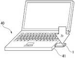
图1是第1实施方式所涉及的半导体存储装置的立体图。FIG. 1 is a perspective view of the semiconductor memory device according to the first embodiment.
图2是表示收存在图1所示的半导体存储装置的内部中的基板和电子部件的立体图。FIG. 2 is a perspective view showing a substrate and electronic components housed in the interior of the semiconductor memory device shown in FIG. 1 .
图3是表示将图1所示的半导体存储装置与主机装置的主连接器连接的状态的立体图。3 is a perspective view showing a state in which the semiconductor memory device shown in FIG. 1 is connected to a main connector of a host device.
图4是表示对于图3所示的与主机装置的主连接器连接后的半导体存储装置从上方作用了外力的状态的说明图。4 is an explanatory diagram showing a state in which an external force acts from above on the semiconductor memory device shown in FIG. 3 after being connected to the main connector of the host device.
图5是表示对于图3所示的与主机装置的主连接器连接后的半导体存储装置从上方作用了外力,基板经由挠性导电部而倾斜的状态的说明图。5 is an explanatory diagram showing a state in which an external force acts from above to the semiconductor memory device connected to the main connector of the host device shown in FIG. 3 , and the substrate is tilted via the flexible conductive portion.
图6是第2实施方式所涉及的半导体存储装置的立体图。6 is a perspective view of a semiconductor memory device according to a second embodiment.
图7是第3实施方式所涉及的半导体存储装置的立体图。7 is a perspective view of a semiconductor memory device according to a third embodiment.
附图标记说明Description of reference numerals
1……半导体存储装置,2……壳体(case),3……模组,5……第1基板,6……闪存(半导体存储器部件),7……控制器(半导体存储器部件),8……第2基板,9……连接器,10……挠性导电部,G……间隙,11……第1壳体主体,12……第2壳体主体,40……主机装置,41……主连接器,50……半导体存储装置,61……间隙,62……基板连接部(挠性导电部),63……布线,71……半导体存储装置,72……突起部,73……凹部,76……嵌合部。1...semiconductor storage device, 2...case, 3...module, 5...first substrate, 6...flash memory (semiconductor memory component), 7...controller (semiconductor memory component), 8...second board, 9...connector, 10...flexible conductive portion, G...gap, 11...first case body, 12...second case body, 40...host device, 41...main connector, 50...semiconductor storage device, 61...gap, 62...substrate connecting portion (flexible conductive portion), 63...wiring, 71...semiconductor storage device, 72...protrusion, 73... Recessed portion, 76... Fitting portion.
具体实施方式Detailed ways
(第1实施方式)(first embodiment)
以下,参照附图说明第1实施方式所涉及的半导体存储装置。Hereinafter, the semiconductor memory device according to the first embodiment will be described with reference to the drawings.
在以下的说明中,针对具有相同或者相似的功能的构成赋予同一标记。另外,有时省略这些构成的重复的说明。在本说明书中,“连接”不限定于以物理性连接的情况,也包含电连接的情况。在本说明书中,“相邻”不限定于相互相邻的情况,也包含作为对象的2个要素之间存在别的要素的情况。In the following description, the same code|symbol is attached|subjected to the structure which has the same or similar function. In addition, the overlapping description of these structures may be abbreviate|omitted. In this specification, "connection" is not limited to the case of physical connection, but also includes the case of electrical connection. In the present specification, "adjacent" is not limited to the case of being adjacent to each other, but also includes a case where another element exists between the two target elements.
图1是表示第1实施方式所涉及的半导体存储装置1的例示性的立体图。FIG. 1 is an exemplary perspective view showing a
图2是表示图1所示的半导体存储装置1的内部构造的例示性的立体图。FIG. 2 is an exemplary perspective view showing the internal structure of the
半导体存储装置1例如也可以称为USB存储器、USB闪存驱动器(UFD)、电子设备、半导体装置、USB设备、存储装置、辅助存储装置、可移动介质。半导体存储装置1也可以是其他装置。The
如图1所示,第1实施方式的半导体存储装置1例如形成为具有扁平的矩形横截面的细长的板状。半导体存储装置1也可以形成为其他形状。As shown in FIG. 1 , the
如图1、图2等所示,在本说明书中定义X轴、Y轴及Z轴。X轴、Y轴、Z轴相互正交。X轴沿着半导体存储装置1的宽度方向。Y轴沿着半导体存储装置1的长度方向。Z轴沿着半导体存储装置1的厚度方向。在本说明书的说明中,为了方便有时沿着Z轴方向标记为上下,沿着Y轴方向标记为左右。As shown in FIG. 1 , FIG. 2 , etc., the X-axis, the Y-axis, and the Z-axis are defined in this specification. The X-axis, Y-axis, and Z-axis are orthogonal to each other. The X axis is along the width direction of the
如图1和图2所示,关于半导体存储装置1,在中空而且Y轴方向细长的扁平形的壳体(case)2的内部收存有模组3。模组3具有第1基板5、闪存(半导体存储器部件)6、控制器(半导体存储器部件)7、第2基板8、连接器9和挠性导电部10。图1作为立体图而表示半导体存储装置1的水平设置状态,表示了将连接器9配置为朝左的状态。图2表示以与图1相同的朝向设置从壳体2取出的模组3的状态。As shown in FIGS. 1 and 2 , in the
此外,连接器9形成为扁平的矩形横截面状,虽然与后述的主机装置的主连接器的朝向也有关,但通常如图1所示,将连接器9以横向长的方式在水平设置状态的姿势下与主连接器连接。因此,图1所示的状态成为与主机装置连接的情况下的半导体存储装置1的基准姿势。In addition, the
壳体2是由硬质的树脂形成的壳体的一例,具有第1壳体主体11和第2壳体主体12。The
第1壳体主体11具有:Y轴方向上较长的长方形状的壳体板13、在该壳体板13的长边侧一体形成的侧壁15、15、以及在壳体板13的短边侧形成的端部壁16、16。通过壳体板13、侧壁15、15以及端部壁16、16划分出薄型的收存空间,在该收存空间中收存模组3的一半厚度左右。The
第2壳体主体12具有:Y轴方向上较长的长方形状的壳体板17、在该壳体板17的长边侧一体形成的侧壁18、18、以及在壳体板17的短边侧形成的端部壁19、19。通过壳体板17、侧壁18、18以及端部壁19、19划分出薄型的收存空间,在该收存空间中收存模组3的一半厚度左右。The
第1壳体主体11与第2壳体主体12具有同等形状。因此,壳体板13与壳体板17的宽度、长度、厚度是同等的,侧壁15与侧壁18的宽度、长度、厚度是同等的,端部壁16、19的宽度、长度、厚度是同等的。The
第1壳体主体11和第2壳体主体12通过使相互的侧壁15、18与相互的端部壁16、19对接,并将对接部分通过超声波熔接等熔接法接合来一体化。通过使第1壳体主体11与第2壳体主体12一体化,构成中空的壳体2,在壳体2的内部收存模组3。使第1壳体主体11与第2壳体主体12一体化的手段不限于熔接,也可以是粘合等其他接合手段,还可以通过凹凸嵌合来接合,通过螺栓、螺丝钉等接合件来接合。The first case
在通过熔接将第1壳体主体11与第2壳体主体12接合的情况下,在相互的侧壁15、18的对接部分和相互的端部壁16、19的对接部分设置熔接部。在通过粘合将第1壳体主体11与第2壳体主体12接合的情况下,在相互的侧壁15、18的对接部分和相互的端部壁16、19的对接部分设置粘合部。When joining the 1st case
图1的例子中,第1壳体主体11与第2壳体主体12通过熔接而一体化,因此侧壁15、18的对接部分和端部壁16、19的对接部分被设为熔接部F。在该方式中,第1壳体主体11和第2壳体主体12具有同等形状,因此上述的熔接部F沿着XY面形成。在本实施方式中,第1基板5和第2基板8被第1壳体主体11和第2壳体主体12包围,该第1壳体主体11和第2壳体主体12配置为从厚度方向一侧和另一侧覆盖第1基板5和第2基板8。In the example of FIG. 1 , since the
在壳体2的长度方向一端侧(左端侧),在端部壁16、19被接合的部分形成有方筒形的突出壁部20。在端部壁16、19被接合的部分形成有与壳体2的内部空间连通的省略图示的开口部,以与该开口部相通的方式形成有突出壁部20。因此,突出壁部20被设置为将壳体2的内部空间与壳体2的外部连通,以经过所述开口部和突出壁部20向外部突出的方式设置有连接器9。On one end side (left end side) in the longitudinal direction of the
通过组合从第1壳体主体11的端部壁16突出的框状的突出片20A和从第2壳体主体12的端部壁19突出的框形的突出片20B,突出壁部20构成为方筒形。与第1壳体主体11和第2壳体主体12通过上述的熔接等被接合的情形同样,突出片20A和突出片20B也是对接部分通过熔接等被接合,而形成方筒形的突出壁部20。By combining the frame-shaped
在壳体2的长度方向另一端侧(右端侧),在端部壁16、19被接合的部分以使壳体2伸长的方式形成有块状的突出部21。突出部21具有:从第1壳体主体11的端部壁16突出的半体突出部21A、以及从第2壳体主体12的端部壁19突出的半体突出部21B。通过将第1壳体主体11与第2壳体主体12接合来一体化,从而半体突出部21A与半体突出部21B被一体化,构成突出部21。突出部21在壳体2的另一端侧以经由周台阶部21d使壳体2延长的方式突出。On the other end side (right end side) in the longitudinal direction of the
突出部21为了安装用于将连接器9覆盖的省略图示的帽部件(盖)而被设置,但也可以省略突出部21。The protruding
在收存于壳体2的内部的第1基板5上,搭载有闪存(存储元件:半导体存储器部件)6和控制器(半导体存储器部件)7。A flash memory (storage element: semiconductor memory component) 6 and a controller (semiconductor memory component) 7 are mounted on the
在图2所示的方式中,在第1基板5的上表面(第1面)安装有控制器7,在第1基板5的下表面(第2面)安装有闪存6。闪存6和控制器7也可以被汇总地设置在第1基板5的上表面和下表面的任一方,也可以被个别地安装在上表面和下表面。In the form shown in FIG. 2 , the
第1基板5例如是印刷电路板(PCB)。第1基板5也可以是像柔性印刷电路板(FPC)那样的其他基板。第1基板5形成为在X-Y平面上扩展的俯视为矩形(四边形状)的板状。第1基板5也可以形成为其他形状。The
闪存6是第1半导体存储器部件的一例,例如也可以称为非易失性存储器、存储器或者存储部。控制器7是第2半导体存储器部件的一例,例如也可以称为控制部。The
闪存6是能够存储信息的电子部件,例如是NAND型闪存。此外,半导体存储装置1也可以包含像NOR型闪存、磁阻存储器(磁阻随机存取存储器(Magnetoresistive RandomAccess Memory:MRAM))、相变存储器(相变随机存取存储器(Phase change Random AccessMemory:PRAM))、电阻变化型存储器(电阻变化型随机存取存储器(Resistive RandomAccess Memory:ReRAM))或者强介电体存储器(强介电体随机存取存储器(Ferroe lectricRandom Access Memory:FeRAM))那样的其他非易失性存储器。The
控制器7如图2所示被安装在基板5的上表面(第1面)。例如,设置于控制器7的多个端子与设置于基板5的上表面的多个电路、电极通过焊料被电连接。控制器7也可以被安装在基板5的下表面(第2面)。控制器7例如对半导体存储装置1进行控制,对半导体存储装置1与后述的图3所示的主机装置40之间的通信进行控制。The
连接器9例如也可以称为插头、插入部或者连接部。The
连接器9经过突出壁部20从壳体2向外部突出,向外部突出的部分例如被能够安装于壳体2的省略图示的帽部件(盖)覆盖。The
连接器9例如是依据USB Type-C规格的公连接器(插头)。USB Type-C规格例如包含USB2.0Type-C规格、USB3.1Gen1Type-C规格及USB3.1Gen2Type-C规格。连接器9具有:由金属制作的扁平方筒形的插入部25、设置于插入部25的内部的连接基板26、以及沿着该连接基板26设置的多根(例如4根)连接端子27。插入部25的内部空间的一半厚度左右由连接基板26占据,在连接基板26中面对插入部25的内部空间一侧配置4个连接端子27的前端侧。The
连接器9的插入部25例如被插入至主机装置侧的USB连接器(母连接器、插座)。此时,连接基板26和连接端子27被插入至主机装置侧的连接口,主机装置侧的连接端子与半导体存储装置1的连接端子27被电连接。由此,能够将半导体存储装置1与主机装置电连接。The
在本实施方式的半导体存储装置1中,在连接器9与第1基板5之间配置有俯视为矩形的第2基板8。第2基板8是在X-Y平面上扩展的俯视为矩形(四边形状)的基板,具有与第1基板5同等的X轴方向宽度,但在Y轴方向上具有第1基板5的几分之一左右的长度。第2基板8如图2所示,形成为X轴方向长度比Y轴方向长度长且俯视为四边形状。第2基板8的宽度(X轴方向的宽度)形成为比连接器9的宽度(X轴方向宽度)稍宽。In the
在第2基板8中,在靠近连接器9的端部侧且是第2基板8的宽度方向(X轴方向)两端部,形成有狭缝状的插通孔30。在连接器9的插入部25中,在靠第2基板8一侧的下缘部形成有供第2基板8的端部插入的缺口部31,在插入部25的面对缺口部31的一部分处以向下突出面对的方式形成有卡止片32。In the
缺口部31以遍及插入部25的下缘部全宽的方式被形成,卡止片32在插入部25的宽度方向两端侧(X轴方向两端侧)分别被形成。The
如图2所示,通过在插通孔30中插入卡止片32并且在缺口部31中插入第2基板8的Y轴方向端部,第2基板8与连接器9连接。As shown in FIG. 2 , the
在第2基板8的上表面侧,设置有与连接器9的4个连接端子27分别连接的端子焊盘33。这些端子焊盘33经由将第2基板8在其厚度方向上贯通的过孔等上下连接导体而从第2基板8的下表面侧延伸出来。On the upper surface side of the
在第2基板8与第1基板5之间设置有比这些基板的厚度稍宽的程度的间隙G,在该间隙G的下方配置有由柔性布线基板等构成的挠性导电部10。在挠性导电部10形成有电气电路,该电气电路与第2基板8的下表面侧的电气电路和第1基板5的下表面侧的电气电路分别通过焊接等连接方法连接。A gap G slightly wider than the thickness of these substrates is provided between the
挠性导电部10的电气电路经由第2基板8的4个端子焊盘33而与连接器9的连接端子27电连接。The electrical circuit of the flexible
挠性导电部10的电气电路在第1基板5的下表面侧延伸出来,与形成于第1基板5的下表面侧的电气电路通过焊料等接合手段被接合。The electrical circuit of the flexible
挠性导电部10作为将连接器9的连接端子27与安装于第1基板5的控制器7、闪存6电连接的连接导体发挥功能。The flexible
挠性导电部10设置在包含作为半导体存储器部件的闪存6和控制器7的第1基板5的基板高度的范围内。The flexible
图1所示的半导体存储装置1与图3所示的笔记本型个人计算机等主机装置40的主连接器41连接来使用。在图3中表示相对于主机装置40的主连接器41连接的半导体存储装置1的状态。The
如图3、图4所示,在桌上等水平面上设置的主机装置40中,主连接器41的插入口沿水平横向设置。因此,半导体存储装置1使连接器9向左而相对于主连接器41的插入口以大致水平朝向在基准姿势下连接。As shown in FIGS. 3 and 4 , in the
在将半导体存储装置1与主机装置40连接来使用的过程中,可以想到如图3、图4的箭头所示,向下的外力意外地作用于半导体存储装置1。In the process of connecting and using the
在该情况下,虽然与作用的外力的大小也有关,但在外力较大的情况下,如图5所示,半导体存储装置1以向下弯折的方式变形。主连接器41中插入的连接器9的插入部25为金属制且强度高,因此大的弯矩力作用于树脂制的壳体2中与连接器9的接合部处。In this case, although it also depends on the magnitude of the applied external force, when the external force is large, as shown in FIG. 5 , the
壳体2是将树脂制的第1壳体主体11与第2壳体主体12熔接而成的构造,因此上述的弯矩力以将第1壳体主体11与第2壳体主体12的熔接部F剥离的方式作用。如果上述的弯矩力比第1壳体主体11与第2壳体主体12的熔接部F的剥离强度小,则半导体存储装置1能够耐受上述的外力。Since the
在上述的弯矩力比第1壳体主体11与第2壳体主体12的熔接部F的剥离强度大的情况下,在连接器9的附近,第1壳体主体11与第2壳体主体12的熔接部F剥离。如果熔接部F剥离,则上述的外力使第1壳体主体11和第2壳体主体12如图5所示以使右端侧向下的方式变形。When the above-mentioned bending moment is larger than the peeling strength of the welded portion F between the first case
由于该变形,连接器9附近的突出片20A与突出片20B分离,壳体2的连接器9周围的熔接部F分离,主要是第2壳体主体12的连接器9周围变形,允许壳体2的倾斜。Due to this deformation, the protruding
在该情况下,第1基板5相对于第2基板8经由挠性导电部10连接,因此虽然第2基板8的姿势不变化,但第1基板5如图5所示以右端部侧向下的方式倾斜。即,通过设置挠性导电部10,能够抑制外力作用于第1基板5,阻止第1基板5的破损。另外,虽然壳体2的熔接部F的一部分剥离,但如果将外力去除,则由于第1壳体主体11与第2壳体主体12的未剥离的剩余的熔接部F的影响,壳体2恢复到变形前的原状态。因此,能够恢复到通过由第1壳体主体11和第2壳体主体12构成的壳体2覆盖第1基板5和第2基板8的原构造。In this case, since the
如以上说明的那样,如果是图1、图2所示的构造的半导体存储装置1,则在与主机装置40连接的状态下,即使万一向下作用了强外力,也仅会使壳体2的熔接部F的一部分剥离而能够防止内部的第1基板5的损坏、折损。As described above, in the case of the
这种半导体存储装置在与主机装置的主连接器连接的状态下,壳体成为向主机装置的外侧突出的状态。因此,如果外力意外地作用于壳体,则外力作用于壳体或者连接器的连接部分,根据负荷的状况,有时造成壳体内的基板破损。In a state of being connected to the main connector of the host device in such a semiconductor memory device, the casing is in a state of protruding to the outside of the host device. Therefore, if an external force acts on the housing unexpectedly, the external force acts on the housing or the connecting portion of the connector, and depending on the state of the load, the substrate in the housing may be damaged.
这会造成半导体存储装置破损,无法从闪存读出信息。This can cause damage to the semiconductor memory device, making it impossible to read information from the flash memory.
相对于此,如果是图1和图2所示的构造的半导体存储装置1,则损坏仅为壳体2的熔接部的一部分剥离,后续能够从闪存6读出信息,也能够向闪存6写入信息。On the other hand, in the
此外,如果超出所需地提高第1壳体主体11与第2壳体主体12的熔接部的强度或者粘合部的强度,则在作用了上述的外力的情况下,有可能造成第1壳体主体11或者第2壳体主体12直接折损。因此,第1壳体主体11与第2壳体主体12的熔接强度或者粘合强度优选设为比第1壳体主体11或者第2壳体主体12的抗折强度低。Furthermore, if the strength of the welded portion or the strength of the adhesive portion between the
即,设为如下构成:在作用了外力的情况下,在第1壳体主体11或者第2壳体主体12折损之前,如图5所示使熔接部F或粘合部剥离。通过设为该构成,本实施方式的半导体存储装置1在作用了外力的情况下如图5所示可靠地变形,能够防止第1基板5的折损。That is, when an external force acts, before the 1st case
图6是表示本发明所涉及的第2实施方式的半导体存储装置的内部构造的立体图。6 is a perspective view showing an internal structure of a semiconductor memory device according to a second embodiment of the present invention.
在第2实施方式的半导体存储装置中,针对与图2所示的第1实施方式的半导体存储装置1相同的构成要素赋予同一标记,省略或者简化同一构成要素的说明。In the semiconductor memory device of the second embodiment, the same components as those of the
在第2实施方式的半导体存储装置中,第1基板5与第2基板8通过缺口部61被分离。缺口部61的部分中在第1基板5与第2基板8之间形成有间隙G。在第1基板5的底部侧(基板的厚度方向下部侧)和第2基板8的底部侧(基板的厚度方向下部侧),设置有基板连接部62。第1基板5的基板底部侧与第2基板8的基板底部侧经由基板连接部62被一体连接。In the semiconductor memory device of the second embodiment, the
第1基板5、第2基板8和基板连接部62由同一基板材料构成。The
第1基板5和第2基板8在形成缺口部61之前,构成为由同一基板材料构成的同一厚度的1个基板,但通过在成为第1基板5和第2基板8的位置的边界部分进行沟槽加工来形成缺口部61,从而具有划分了第1基板5和第2基板8的构造。The
基板连接部62例如厚度为0.2~0.3mm左右,基板连接部62例如具有能够大致数次弯曲的程度的挠性。另外,在基板连接部62中,装入有对第1基板5中形成的电气电路与第2基板8中形成的电气电路进行连接的布线63。因此,基板连接部62具有与第1实施方式的挠性导电部10相似的挠曲性,基板连接部62兼作挠性导电部。The thickness of the
如果是具有图6所示的内部构造的半导体存储装置,则能够得到与第1实施方式的半导体存储装置1同样的作用效果。即,在与主机装置40的主连接器41连接的状态下,如果向下作用了强外力,则虽然壳体2的熔接部F发生部分剥离,壳体2发生部分变形,但基板连接部62弯曲。由此,允许壳体2内的第1基板5倾斜,能够防止第1基板5的损坏。In the case of the semiconductor memory device having the internal structure shown in FIG. 6 , the same functions and effects as those of the
此外,基板连接部62例如具有能够大致数次弯曲的程度的挠性,但如果反复弯折则有可能损坏。因此,优选在与主机装置40连接的状态下向下作用了一次强外力的情况下,尽可能迅速地从闪存6读出信息。另外,优选将该读出信息向主机装置40的SSD(固态驱动器)或者HDD(硬盘驱动器)等存储装置复制。In addition, the
图7是表示本发明所涉及的第3实施方式的半导体存储装置的立体图。7 is a perspective view showing a semiconductor memory device according to a third embodiment of the present invention.
在第3实施方式的半导体存储装置中,针对与图2所示的第1实施方式的半导体存储装置1相同的构成要素赋予同一标记,省略或者简化同一构成要素的说明。In the semiconductor memory device of the third embodiment, the same components as those of the
在第3实施方式的半导体存储装置71中,壳体2的内部中收存的模组3的构造与第1实施方式的半导体存储装置1是同等的。即,模组3具有第1基板5、闪存6、控制器7、第2基板8、连接器9和挠性导电部10,这些构造与第1实施方式的半导体存储装置1是同等的。In the
在第3实施方式的半导体存储装置中,壳体2的构造与第1实施方式的构造不同。在壳体2中,基本构造与第1实施方式是同等的,第1壳体主体11和第2壳体主体12具有侧壁15、18和端部壁16、19,具有突出壁部20和突出部21,该构造也是同等的。第1壳体主体11与第2壳体主体12通过之前说明的熔接或者粘合等接合方法被接合,该构造也是同等的。In the semiconductor memory device of the third embodiment, the structure of the
在第3实施方式的壳体2中,不同点是,在第1壳体主体11的内部侧4处形成有向下的突起部72,在第2壳体主体12的内部侧4处形成有朝向上表面侧的凹部73。突起部72从第1壳体主体11的壳体板13的下表面侧形成的厚壁部74向下突出。凹部73被形成于第2壳体主体12的壳体板17的上表面侧形成的厚壁部75的上表面侧。The
在壳体2中,靠近端部壁16、19侧的突起部72和凹部73被形成于端部壁16与侧壁15交叉的角部分的内侧、以及端部壁19与侧壁18交叉的角部分的内侧。在壳体2中,靠近连接器9侧的突起部72和凹部73在第1基板5与第2基板8的边界且面对间隙G的位置处,以夹着基板连接部62的两侧的方式形成。In the
在第1基板5与第2基板8的边界部分设置有间隙G和挠性导电部10,因此作为一例,将挠性导电部10的宽度形成得比第1基板的宽度稍小。由此,能够成为如下构成:将使挠性导电部10变窄的量与间隙G合起来,易于确保厚壁部74、75的设置空间。Since the gap G and the flexible
第3实施方式的壳体2除了将第1壳体主体11与第2壳体主体12熔接或者粘合的构造以外,还将各突起部72与各凹部73嵌合来构成嵌合部76,由此将第1壳体主体11与第2壳体主体12接合。In the
在将具备第3实施方式的壳体2的半导体存储装置71如图3所示与主机装置40的主连接器41连接,并作用了向下的外力的情况下,与图5所示的情况同样,连接器9附近的熔接部F部分剥离。在该情况下,第1壳体主体11和第2壳体主体12变形,并且由于挠性导电部10的作用,第1基板5能够向下倾斜,这一点也与第1实施方式是同样的。When the
在与图5所示的情况同样作用了外力的情况下,随着第1壳体主体11和第2壳体主体12的变形,连接器9附近的突起部72从凹部73脱离,或者突起部72从凹部73被部分拔出,凹凸嵌合力变弱。When an external force acts as in the case shown in FIG. 5 , along with the deformation of the
在此,如果去除来自外部的外力,半导体存储装置71相对于主连接器41的姿势恢复平行,则从主连接器41拔出半导体存储装置71,将从连接器9附近的凹部73脱离的突起部72重新嵌合至凹部73。或者,将从连接器9附近的凹部73脱离过程中的突起部72重新嵌合至凹部73。Here, when the external force from the outside is removed and the posture of the
由此,能够使第1壳体主体11与第2壳体主体12的嵌合状态复原,使壳体2复原到接近原状态。Thereby, the fitted state of the
半导体存储装置71具备如下构成:具备除了第1壳体主体11与第2壳体主体12的熔接或者粘合之外还通过凹部73与突起部72的凹凸嵌合而一体化的壳体2。The
如果是该构成的半导体存储装置71,则在作用了外力的情况下假设壳体2的接合部的一部分剥离,通过突起部72相对于凹部73再嵌合,具有能够可靠地使壳体2的状态复原的效果。In the
此外,第1壳体主体11和第2壳体主体12中的突起部72和凹部73的设置位置不限于图7所示的例子。In addition, the installation position of the
在图7的例子中,在壳体2中在第1壳体主体11侧设置了突起部72,在第2壳体主体12侧设置了凹部73,但也可以在第1壳体主体11侧设置凹部73,在第2壳体主体12侧设置突起部72。In the example of FIG. 7 , the protruding
在设置多个突起部72和多个凹部73的情况下,也能够将一部分的突起部72设置于第1壳体主体11,将剩余的突起部72设置于第2壳体主体12侧。也能够在与第1壳体主体11上设置的突起部72对置的第2壳体主体12侧设置凹部73,在与第1壳体主体11中设置的凹部73对置的第2壳体主体12侧设置突起部72。When the plurality of
设置于第1壳体主体11和第2壳体主体12的突起部72的数量和凹部73的数量不特别限制,能够设置所需的个数,关于设置位置也只要在壳体2的内部即可,可以是任意的位置。The number of the
此外,上述的实施方式中使用的挠性导电部作为由柔性基板或一般性的基板材料构成的挠性导电部进行了说明,但挠性导电部也可以使用绝缘包覆的多根柔性导电线缆。通过经由多根导电线缆将第1基板5与第2基板8电连接、且在第1基板5与第2基板8之间设置间隙的构造,能够得到与之前的实施方式同样的效果。In addition, the flexible conductive portion used in the above-described embodiment has been described as a flexible conductive portion made of a flexible substrate or a general substrate material, but a plurality of insulating-coated flexible conductive wires may be used for the flexible conductive portion. cable. By the structure in which the
以上,关于多个实施方式及变形例进行了说明,但实施方式不限定于上述例子。例如,上述2个以上的实施方式及变形例也可以相互组合来实现。As mentioned above, although several embodiment and modification were demonstrated, embodiment is not limited to the said example. For example, two or more of the above-described embodiments and modifications may be implemented in combination with each other.
另外,在之前的实施方式中,在将第1壳体主体11与第2壳体主体12接合的情况下,也可以对两者不进行熔接或粘合,而仅通过利用了上述的凹部和突起部的凹凸嵌合来接合。In addition, in the previous embodiment, when the first case
以上,关于本发明的多个实施方式进行了说明,但这些实施方式作为例子而提示,意图不在于限定发明的范围。这些实施方式能够以其他各种方式实施,在不脱离发明的主旨的范围内能够进行各种省略、置换、变更。这些实施方式及其变形例被包含在发明的范围和主旨中,同样被包含在权利要求书所记载的发明及其等同的范围中。As mentioned above, although several embodiment of this invention was described, these embodiment is shown as an example, Comprising: It does not intend to limit the range of invention. These embodiments can be implemented in various other forms, and various omissions, substitutions, and changes can be made without departing from the gist of the invention. These embodiments and their modifications are included in the scope and spirit of the invention, and are also included in the invention described in the claims and their equivalents.
Claims (9)
Applications Claiming Priority (2)
| Application Number | Priority Date | Filing Date | Title |
|---|---|---|---|
| JP2021042683AJP2022142496A (en) | 2021-03-16 | 2021-03-16 | semiconductor storage device |
| JP2021-042683 | 2021-03-16 |
Publications (1)
| Publication Number | Publication Date |
|---|---|
| CN115081573Atrue CN115081573A (en) | 2022-09-20 |
Family
ID=83245840
Family Applications (1)
| Application Number | Title | Priority Date | Filing Date |
|---|---|---|---|
| CN202110811894.2AWithdrawnCN115081573A (en) | 2021-03-16 | 2021-07-19 | Semiconductor memory device with a plurality of memory cells |
Country Status (4)
| Country | Link |
|---|---|
| US (1) | US20220302660A1 (en) |
| JP (1) | JP2022142496A (en) |
| CN (1) | CN115081573A (en) |
| TW (1) | TWI837477B (en) |
Families Citing this family (1)
| Publication number | Priority date | Publication date | Assignee | Title |
|---|---|---|---|---|
| CN116526176B (en)* | 2023-07-03 | 2023-09-12 | 四川和恩泰半导体有限公司 | USB connects and USB flash disk equipment system |
Citations (6)
| Publication number | Priority date | Publication date | Assignee | Title |
|---|---|---|---|---|
| TWM249297U (en)* | 2003-12-12 | 2004-11-01 | Megaforce Co Ltd | Thin USB plug connector having fool-proof design |
| US20050070138A1 (en)* | 2003-09-11 | 2005-03-31 | Super Talent Electronics Inc. | Slim USB Plug and Flash-Memory Card with Supporting Underside Ribs Engaging Socket Springs |
| US20120194990A1 (en)* | 2011-01-31 | 2012-08-02 | Martin Kuster | Semiconductor Arrangements |
| CN110739297A (en)* | 2018-07-18 | 2020-01-31 | 东芝存储器株式会社 | semiconductor memory device |
| US20200067228A1 (en)* | 2016-12-22 | 2020-02-27 | Sony Corporation | Electronic apparatus and connector |
| US20200287335A1 (en)* | 2019-03-05 | 2020-09-10 | Yi-Fang CHUANG | Connector having one-piece housing |
Family Cites Families (2)
| Publication number | Priority date | Publication date | Assignee | Title |
|---|---|---|---|---|
| TWI539258B (en)* | 2012-08-28 | 2016-06-21 | 宏碁股份有限公司 | Universal serial bus connector and electronic device using the universal serial bus connector |
| TWM538616U (en)* | 2016-11-21 | 2017-03-21 | shao-qing Zeng | Transmitter with storage function and capable of using magnetic force to form a folded state |
- 2021
- 2021-03-16JPJP2021042683Apatent/JP2022142496A/enactivePending
- 2021-05-28TWTW110119403Apatent/TWI837477B/enactive
- 2021-06-15USUS17/347,886patent/US20220302660A1/ennot_activeAbandoned
- 2021-07-19CNCN202110811894.2Apatent/CN115081573A/ennot_activeWithdrawn
Patent Citations (6)
| Publication number | Priority date | Publication date | Assignee | Title |
|---|---|---|---|---|
| US20050070138A1 (en)* | 2003-09-11 | 2005-03-31 | Super Talent Electronics Inc. | Slim USB Plug and Flash-Memory Card with Supporting Underside Ribs Engaging Socket Springs |
| TWM249297U (en)* | 2003-12-12 | 2004-11-01 | Megaforce Co Ltd | Thin USB plug connector having fool-proof design |
| US20120194990A1 (en)* | 2011-01-31 | 2012-08-02 | Martin Kuster | Semiconductor Arrangements |
| US20200067228A1 (en)* | 2016-12-22 | 2020-02-27 | Sony Corporation | Electronic apparatus and connector |
| CN110739297A (en)* | 2018-07-18 | 2020-01-31 | 东芝存储器株式会社 | semiconductor memory device |
| US20200287335A1 (en)* | 2019-03-05 | 2020-09-10 | Yi-Fang CHUANG | Connector having one-piece housing |
Also Published As
| Publication number | Publication date |
|---|---|
| US20220302660A1 (en) | 2022-09-22 |
| TWI837477B (en) | 2024-04-01 |
| JP2022142496A (en) | 2022-09-30 |
| TW202238405A (en) | 2022-10-01 |
Similar Documents
| Publication | Publication Date | Title |
|---|---|---|
| KR101221813B1 (en) | Connector | |
| CN105957855B (en) | Semiconductor device and storage system | |
| TWI617103B (en) | Electronic machine | |
| CN108886873A (en) | multilayer circuit board | |
| US8422236B2 (en) | Pin module and chip on board type use device | |
| TWI691130B (en) | Modular plug-in connector, replaceable module printed circuit board | |
| CN102858090B (en) | Semiconductor device | |
| CN115081573A (en) | Semiconductor memory device with a plurality of memory cells | |
| JP2002280690A (en) | Printed wiring board and connection structure thereof | |
| EP3982495A1 (en) | Electronic device including host connector and memory device | |
| CN105551515A (en) | Semiconductor memory device | |
| TWI820788B (en) | memory system | |
| US9526186B2 (en) | Storage device and producing method of the same | |
| US6966785B2 (en) | Connector | |
| TW200820843A (en) | Flexible printed circuit | |
| US9367712B1 (en) | High density memory card using folded flex | |
| US20240397627A1 (en) | Board unit, memory system, and electronic device | |
| CN105427878B (en) | Usb storage device | |
| CN101859589B (en) | Compact Flash storage device | |
| CN108808288A (en) | Card connector | |
| TWI221346B (en) | Electrical connector suitable for plural types of electronic cards and electronic device using the same | |
| TWM272266U (en) | Slim USB electronic device | |
| JP3960071B2 (en) | Electronic equipment | |
| JP4367797B2 (en) | connector | |
| JP2025012244A (en) | Connection terminal and connector device |
Legal Events
| Date | Code | Title | Description |
|---|---|---|---|
| PB01 | Publication | ||
| PB01 | Publication | ||
| SE01 | Entry into force of request for substantive examination | ||
| SE01 | Entry into force of request for substantive examination | ||
| WW01 | Invention patent application withdrawn after publication | Application publication date:20220920 | |
| WW01 | Invention patent application withdrawn after publication |