CN115053341A - Semiconductor memory device with a plurality of memory cells - Google Patents
Semiconductor memory device with a plurality of memory cellsDownload PDFInfo
- Publication number
- CN115053341A CN115053341ACN202080008618.6ACN202080008618ACN115053341ACN 115053341 ACN115053341 ACN 115053341ACN 202080008618 ACN202080008618 ACN 202080008618ACN 115053341 ACN115053341 ACN 115053341A
- Authority
- CN
- China
- Prior art keywords
- conductor
- memory device
- layer
- conductor layers
- semiconductor
- Prior art date
- Legal status (The legal status is an assumption and is not a legal conclusion. Google has not performed a legal analysis and makes no representation as to the accuracy of the status listed.)
- Pending
Links
Images


Classifications
- H—ELECTRICITY
- H10—SEMICONDUCTOR DEVICES; ELECTRIC SOLID-STATE DEVICES NOT OTHERWISE PROVIDED FOR
- H10B—ELECTRONIC MEMORY DEVICES
- H10B41/00—Electrically erasable-and-programmable ROM [EEPROM] devices comprising floating gates
- H10B41/10—Electrically erasable-and-programmable ROM [EEPROM] devices comprising floating gates characterised by the top-view layout
- H—ELECTRICITY
- H01—ELECTRIC ELEMENTS
- H01L—SEMICONDUCTOR DEVICES NOT COVERED BY CLASS H10
- H01L21/00—Processes or apparatus adapted for the manufacture or treatment of semiconductor or solid state devices or of parts thereof
- H01L21/70—Manufacture or treatment of devices consisting of a plurality of solid state components formed in or on a common substrate or of parts thereof; Manufacture of integrated circuit devices or of parts thereof
- H01L21/71—Manufacture of specific parts of devices defined in group H01L21/70
- H01L21/768—Applying interconnections to be used for carrying current between separate components within a device comprising conductors and dielectrics
- H01L21/76801—Applying interconnections to be used for carrying current between separate components within a device comprising conductors and dielectrics characterised by the formation and the after-treatment of the dielectrics, e.g. smoothing
- H01L21/76802—Applying interconnections to be used for carrying current between separate components within a device comprising conductors and dielectrics characterised by the formation and the after-treatment of the dielectrics, e.g. smoothing by forming openings in dielectrics
- H—ELECTRICITY
- H01—ELECTRIC ELEMENTS
- H01L—SEMICONDUCTOR DEVICES NOT COVERED BY CLASS H10
- H01L21/00—Processes or apparatus adapted for the manufacture or treatment of semiconductor or solid state devices or of parts thereof
- H01L21/70—Manufacture or treatment of devices consisting of a plurality of solid state components formed in or on a common substrate or of parts thereof; Manufacture of integrated circuit devices or of parts thereof
- H01L21/71—Manufacture of specific parts of devices defined in group H01L21/70
- H01L21/768—Applying interconnections to be used for carrying current between separate components within a device comprising conductors and dielectrics
- H01L21/76838—Applying interconnections to be used for carrying current between separate components within a device comprising conductors and dielectrics characterised by the formation and the after-treatment of the conductors
- H01L21/76841—Barrier, adhesion or liner layers
- H01L21/76843—Barrier, adhesion or liner layers formed in openings in a dielectric
- H—ELECTRICITY
- H01—ELECTRIC ELEMENTS
- H01L—SEMICONDUCTOR DEVICES NOT COVERED BY CLASS H10
- H01L21/00—Processes or apparatus adapted for the manufacture or treatment of semiconductor or solid state devices or of parts thereof
- H01L21/70—Manufacture or treatment of devices consisting of a plurality of solid state components formed in or on a common substrate or of parts thereof; Manufacture of integrated circuit devices or of parts thereof
- H01L21/71—Manufacture of specific parts of devices defined in group H01L21/70
- H01L21/768—Applying interconnections to be used for carrying current between separate components within a device comprising conductors and dielectrics
- H01L21/76838—Applying interconnections to be used for carrying current between separate components within a device comprising conductors and dielectrics characterised by the formation and the after-treatment of the conductors
- H01L21/76877—Filling of holes, grooves or trenches, e.g. vias, with conductive material
- H—ELECTRICITY
- H01—ELECTRIC ELEMENTS
- H01L—SEMICONDUCTOR DEVICES NOT COVERED BY CLASS H10
- H01L23/00—Details of semiconductor or other solid state devices
- H01L23/52—Arrangements for conducting electric current within the device in operation from one component to another, i.e. interconnections, e.g. wires, lead frames
- H01L23/522—Arrangements for conducting electric current within the device in operation from one component to another, i.e. interconnections, e.g. wires, lead frames including external interconnections consisting of a multilayer structure of conductive and insulating layers inseparably formed on the semiconductor body
- H01L23/5226—Via connections in a multilevel interconnection structure
- H—ELECTRICITY
- H01—ELECTRIC ELEMENTS
- H01L—SEMICONDUCTOR DEVICES NOT COVERED BY CLASS H10
- H01L23/00—Details of semiconductor or other solid state devices
- H01L23/52—Arrangements for conducting electric current within the device in operation from one component to another, i.e. interconnections, e.g. wires, lead frames
- H01L23/522—Arrangements for conducting electric current within the device in operation from one component to another, i.e. interconnections, e.g. wires, lead frames including external interconnections consisting of a multilayer structure of conductive and insulating layers inseparably formed on the semiconductor body
- H01L23/532—Arrangements for conducting electric current within the device in operation from one component to another, i.e. interconnections, e.g. wires, lead frames including external interconnections consisting of a multilayer structure of conductive and insulating layers inseparably formed on the semiconductor body characterised by the materials
- H01L23/53204—Conductive materials
- H01L23/53209—Conductive materials based on metals, e.g. alloys, metal silicides
- H01L23/53257—Conductive materials based on metals, e.g. alloys, metal silicides the principal metal being a refractory metal
- H01L23/53266—Additional layers associated with refractory-metal layers, e.g. adhesion, barrier, cladding layers
- H—ELECTRICITY
- H01—ELECTRIC ELEMENTS
- H01L—SEMICONDUCTOR DEVICES NOT COVERED BY CLASS H10
- H01L23/00—Details of semiconductor or other solid state devices
- H01L23/52—Arrangements for conducting electric current within the device in operation from one component to another, i.e. interconnections, e.g. wires, lead frames
- H01L23/522—Arrangements for conducting electric current within the device in operation from one component to another, i.e. interconnections, e.g. wires, lead frames including external interconnections consisting of a multilayer structure of conductive and insulating layers inseparably formed on the semiconductor body
- H01L23/532—Arrangements for conducting electric current within the device in operation from one component to another, i.e. interconnections, e.g. wires, lead frames including external interconnections consisting of a multilayer structure of conductive and insulating layers inseparably formed on the semiconductor body characterised by the materials
- H01L23/53204—Conductive materials
- H01L23/53271—Conductive materials containing semiconductor material, e.g. polysilicon
- H—ELECTRICITY
- H10—SEMICONDUCTOR DEVICES; ELECTRIC SOLID-STATE DEVICES NOT OTHERWISE PROVIDED FOR
- H10B—ELECTRONIC MEMORY DEVICES
- H10B41/00—Electrically erasable-and-programmable ROM [EEPROM] devices comprising floating gates
- H10B41/20—Electrically erasable-and-programmable ROM [EEPROM] devices comprising floating gates characterised by three-dimensional arrangements, e.g. with cells on different height levels
- H10B41/23—Electrically erasable-and-programmable ROM [EEPROM] devices comprising floating gates characterised by three-dimensional arrangements, e.g. with cells on different height levels with source and drain on different levels, e.g. with sloping channels
- H10B41/27—Electrically erasable-and-programmable ROM [EEPROM] devices comprising floating gates characterised by three-dimensional arrangements, e.g. with cells on different height levels with source and drain on different levels, e.g. with sloping channels the channels comprising vertical portions, e.g. U-shaped channels
- H—ELECTRICITY
- H10—SEMICONDUCTOR DEVICES; ELECTRIC SOLID-STATE DEVICES NOT OTHERWISE PROVIDED FOR
- H10B—ELECTRONIC MEMORY DEVICES
- H10B41/00—Electrically erasable-and-programmable ROM [EEPROM] devices comprising floating gates
- H10B41/50—Electrically erasable-and-programmable ROM [EEPROM] devices comprising floating gates characterised by the boundary region between the core region and the peripheral circuit region
- H—ELECTRICITY
- H10—SEMICONDUCTOR DEVICES; ELECTRIC SOLID-STATE DEVICES NOT OTHERWISE PROVIDED FOR
- H10B—ELECTRONIC MEMORY DEVICES
- H10B43/00—EEPROM devices comprising charge-trapping gate insulators
- H10B43/10—EEPROM devices comprising charge-trapping gate insulators characterised by the top-view layout
- H—ELECTRICITY
- H10—SEMICONDUCTOR DEVICES; ELECTRIC SOLID-STATE DEVICES NOT OTHERWISE PROVIDED FOR
- H10B—ELECTRONIC MEMORY DEVICES
- H10B43/00—EEPROM devices comprising charge-trapping gate insulators
- H10B43/20—EEPROM devices comprising charge-trapping gate insulators characterised by three-dimensional arrangements, e.g. with cells on different height levels
- H10B43/23—EEPROM devices comprising charge-trapping gate insulators characterised by three-dimensional arrangements, e.g. with cells on different height levels with source and drain on different levels, e.g. with sloping channels
- H10B43/27—EEPROM devices comprising charge-trapping gate insulators characterised by three-dimensional arrangements, e.g. with cells on different height levels with source and drain on different levels, e.g. with sloping channels the channels comprising vertical portions, e.g. U-shaped channels
- H—ELECTRICITY
- H10—SEMICONDUCTOR DEVICES; ELECTRIC SOLID-STATE DEVICES NOT OTHERWISE PROVIDED FOR
- H10B—ELECTRONIC MEMORY DEVICES
- H10B43/00—EEPROM devices comprising charge-trapping gate insulators
- H10B43/50—EEPROM devices comprising charge-trapping gate insulators characterised by the boundary region between the core and peripheral circuit regions
Landscapes
- Engineering & Computer Science (AREA)
- Physics & Mathematics (AREA)
- Condensed Matter Physics & Semiconductors (AREA)
- General Physics & Mathematics (AREA)
- Computer Hardware Design (AREA)
- Microelectronics & Electronic Packaging (AREA)
- Power Engineering (AREA)
- Manufacturing & Machinery (AREA)
- Semiconductor Memories (AREA)
- Non-Volatile Memory (AREA)
Abstract
Description
Translated fromChinese技术领域technical field
实施方式涉及半导体存储装置。Embodiments relate to semiconductor memory devices.
背景技术Background technique
已知存在能够非易失性地存储数据的NAND型闪速存储器。There are known NAND-type flash memories capable of storing data nonvolatilely.
现有技术文献prior art literature
专利文献Patent Literature
专利文献1:美国专利第8581330号说明书Patent Document 1: Specification of US Patent No. 8581330
发明内容SUMMARY OF THE INVENTION
发明所要解决的问题The problem to be solved by the invention
提供高品质的半导体存储装置。Provides high-quality semiconductor memory devices.
用于解决问题的手段means to solve the problem
实施方式的半导体存储装置具备多个第一导体层、多个绝缘膜、半导体层、电荷储存层、多个第二导体层和多个接触插塞,上述多个第一导体层沿第一方向层叠,并且分别包含钨,上述多个绝缘膜包含与上述多个第一导体层交替层叠的层叠部和相对于上述层叠部向与上述第一方向正交的第二方向突出的第一突出部,上述半导体层使多个上述层叠部与上述多个第一导体层的层叠体内沿上述第一方向延伸,上述电荷储存层配置于上述多个第一导体层与上述半导体层之间,上述多个第二导体层在上述绝缘膜处的上述第一突出部之上与上述第一导体层相接地配置,并且具有包含杂质的硅,上述多个接触插塞在上述多个第二导体层之中的一个第二导体层之上与上述一个第二导体相接地设置,具有导电性,并且沿上述第一方向延伸。The semiconductor memory device of the embodiment includes a plurality of first conductor layers, a plurality of insulating films, a semiconductor layer, a charge storage layer, a plurality of second conductor layers, and a plurality of contact plugs, and the plurality of first conductor layers are along the first direction laminated and each containing tungsten, the plurality of insulating films including laminated portions alternately laminated with the plurality of first conductor layers, and first protruding portions protruding in a second direction orthogonal to the first direction with respect to the laminated portion The semiconductor layer extends in the first direction in a laminate of the plurality of laminate portions and the plurality of first conductor layers, the charge storage layer is disposed between the plurality of first conductor layers and the semiconductor layer, and the plurality of A plurality of second conductor layers are arranged in contact with the first conductor layers on the first protrusions in the insulating film, and include silicon containing impurities, and the plurality of contact plugs are inserted into the plurality of second conductor layers. One of the second conductor layers is provided in contact with the above-mentioned one of the second conductors, has conductivity, and extends along the above-mentioned first direction.
附图说明Description of drawings
图1是表示实施方式的半导体存储装置1的构成例的模块图。FIG. 1 is a block diagram showing a configuration example of a
图2是表示实施方式的半导体存储装置1所具备的存储单元阵列10的构成的电路图。FIG. 2 is a circuit diagram showing the configuration of the
图3是表示实施方式的半导体存储装置1所具备的存储单元阵列10的布局的俯视图。3 is a plan view showing the layout of the
图4是表示与图3中的C所示的单元区域C1的一部分相关的布局的俯视图。FIG. 4 is a plan view showing a layout related to a part of the cell region C1 shown by C in FIG. 3 .
图5是表示实施方式的半导体存储装置1中的单元区域C1的结构的剖视图。5 is a cross-sectional view showing the structure of a cell region C1 in the
图6是表示实施方式的半导体存储装置1中的存储器柱MP的结构的剖视图。FIG. 6 is a cross-sectional view showing the structure of the memory pillar MP in the
图7是表示图3中的存储单元阵列10的结构的A-A’剖视图。Fig. 7 is an A-A' cross-sectional view showing the structure of the
图8是表示图3中的存储单元阵列10的结构的B-B’剖视图。Fig. 8 is a B-B' cross-sectional view showing the structure of the
图9是表示实施方式的半导体存储装置1所具备的存储单元阵列10的字线WL6剖面的俯视图。9 is a plan view showing a cross section of a word line WL6 of the
图10是用于对实施方式的半导体存储装置1的制造工序进行说明的流程图。FIG. 10 is a flowchart for explaining a manufacturing process of the
图11是用于对实施方式的半导体存储装置1的制造工序进行说明的存储单元阵列10的剖视图。11 is a cross-sectional view of the
图12是用于对实施方式的半导体存储装置1的制造工序进行说明的存储单元阵列10的剖视图。12 is a cross-sectional view of the
图13是用于对实施方式的半导体存储装置1的制造工序进行说明的存储单元阵列10的剖视图。13 is a cross-sectional view of the
图14是用于对实施方式的半导体存储装置1的制造工序进行说明的存储单元阵列10的剖视图。14 is a cross-sectional view of the
图15是用于对实施方式的半导体存储装置1的制造工序进行说明的存储单元阵列10的剖视图。15 is a cross-sectional view of the
图16是用于对实施方式的半导体存储装置1的制造工序进行说明的存储单元阵列10的剖视图。16 is a cross-sectional view of the
图17是用于对比较例的半导体存储装置1的制造工序进行说明的流程图。FIG. 17 is a flowchart for explaining the manufacturing process of the
图18是用于对比较例的半导体存储装置1的制造工序进行说明的存储单元阵列10的剖视图。FIG. 18 is a cross-sectional view of the
图19是用于对比较例的半导体存储装置1的制造工序进行说明的存储单元阵列10的剖视图。FIG. 19 is a cross-sectional view of the
图20是用于对比较例的半导体存储装置1的制造工序进行说明的存储单元阵列10的剖视图。FIG. 20 is a cross-sectional view of the
图21是用于对比较例的半导体存储装置1的制造工序进行说明的存储单元阵列10的剖视图。21 is a cross-sectional view of the
图22是用于对比较例的半导体存储装置1的制造工序进行说明的存储单元阵列10的剖视图。22 is a cross-sectional view of the
图23是表示图22中的D所示存储单元阵列10的结构的剖视图。FIG. 23 is a cross-sectional view showing the structure of the
具体实施方式Detailed ways
以下,参照附图对实施方式进行说明。各实施方式例示了用于将发明的技术构思具体化的装置、方法。附图为示意图或概念图,各附图的尺寸及比率等并不限于与现实的尺寸及比率相同。本发明的技术构思并不被构成要素的形状、结构、配置等限定。Hereinafter, embodiments will be described with reference to the drawings. The respective embodiments illustrate apparatuses and methods for embodying the technical idea of the invention. The drawings are schematic or conceptual diagrams, and the dimensions and ratios of the drawings are not limited to the same as the actual dimensions and ratios. The technical idea of the present invention is not limited by the shape, structure, arrangement, etc. of the constituent elements.
<1>实施方式<1> Embodiment
图1示出了实施方式的半导体存储装置1的构成例。以下,对实施方式的半导体存储装置1进行说明。FIG. 1 shows a configuration example of a
<1-1>半导体存储装置1的构成<1-1> Configuration of
<1-1-1>半导体存储装置1的整体构成<1-1-1> Overall Configuration of
半导体存储装置1例如是能够非易失性地存储数据的NAND型闪速存储器。半导体存储装置1例如由外部的存储控制器2控制。The
如图1所示,半导体存储装置1例如包含存储单元阵列10、指令寄存器11、地址寄存器12、序列发生器13、驱动模块14、行解码器模块15及读出放大器模块16。As shown in FIG. 1 , the
存储单元阵列10包含多个区块BLK0~BLKn(n为1以上的整数)。区块BLK是能够非易失性地存储数据的多个存储单元的集合,例如作为数据的消除单位使用。The
另外,存储单元阵列10中设置有多个位线及多个字线。各存储单元例如与一根位线和一根字线有关。对存储单元阵列10的详细构成在后面进行叙述。In addition, a plurality of bit lines and a plurality of word lines are provided in the
指令寄存器11对半导体存储装置1由存储控制器2接收的指令CMD进行保持。指令CMD例如包含使序列发生器13执行读取操作、写入操作、消除操作等的指令。The command register 11 holds the command CMD received by the
地址寄存器12对半导体存储装置1由存储控制器2接收的地址信息ADD进行保持。地址信息ADD例如包含块地址BA、页面地址PA及列地址CA。块地址BA、页面地址PA及列地址CA例如分别用于选择区块BLK、字线及位线。The
序列发生器13对半导体存储装置1整体的操作进行控制。序列发生器13例如基于保持于指令寄存器11的指令CMD而对驱动模块14、行解码器模块15及读出放大器模块16等进行控制,由此执行读取操作、写入操作、消除操作等。The
驱动模块14产生用于读取操作、写入操作、消除操作等的电压。而且,驱动模块14例如基于保持于地址寄存器12的页面地址PA对所选择的字线相对应的信号线施加所产生的电压。The drive module 14 generates voltages for read operations, write operations, erase operations, and the like. Then, the driving module 14 applies the generated voltage to the signal line corresponding to the selected word line based on, for example, the page address PA held in the
行解码器模块15基于保持于地址寄存器12的块地址BA来选择相对应的存储单元阵列10内的一个区块BLK。而且,行解码器模块15例如将施加于与所选择的字线相对应的信号线的电压转送至所选择的区块BLK内的所选择的字线。The
就读出放大器模块16来说,在写入操作中,与由存储控制器2接收的写入数据DAT相对应地对各位线施加所期望的电压。另外,就读出放大器模块16来说,在读取操作中,基于位线的电压来判定存储单元所存储的数据,读取判定结果并作为数据DAT转送至存储控制器2。As far as the
半导体存储装置1与存储控制器2之间的通信例如支持NAND接口规格。例如,半导体存储装置1与存储控制器2之间的通信使用指令锁存使能信号CLE、地址锁存使能信号ALE、写入使能信号WEn、读取使能信号REn、就绪忙信号RBn及输入输出信号I/O。Communication between the
指令锁存使能信号CLE是表示半导体存储装置1接收的输入输出信号I/O为指令CMD的信号。地址锁存使能信号ALE是表示半导体存储装置1接收的信号I/O为地址信息ADD的信号。写入使能信号WEn是对半导体存储装置1命令进行输入输出信号I/O的输入的信号。读取使能信号REn是对半导体存储装置1命令进行输入输出信号I/O的输出的信号。The command latch enable signal CLE is a signal indicating that the input/output signal I/O received by the
就绪忙信号RBn是将半导体存储装置1为接收来自存储控制器2的命令的就绪状态还是为不接收命令的繁忙状态通知给存储控制器2的信号。输入输出信号I/O例如是八位宽的信号,可以包含指令CMD、地址信息ADD、数据DAT等。The ready busy signal RBn is a signal for notifying the
以上进行了说明的半导体存储装置1及存储控制器2可以由它们的组合构成一个半导体存储装置。作为这样的半导体存储装置,例如可以列举出SDTM卡之类的存储卡、SSD(固态存储器;solid state drive)等。The
<1-1-2>存储单元阵列10的电路构成<1-1-2> Circuit Configuration of
图2是实施方式的半导体存储装置1所具备的存储单元阵列10的电路构成,抽出并示出了存储单元阵列10所包含的多个区块BL之中一个区块BLK。2 is a circuit configuration of a
如图2所示,区块BLK例如包含四个字符串单元SU0~SU3。各字符串单元SU包含多个NAND字符串NS。As shown in FIG. 2, the block BLK includes, for example, four character string units SU0-SU3. Each character string unit SU includes a plurality of NAND character strings NS.
多个NAND字符串NS分别与位线BL0~BLm(m为1以上的整数)相关联。各NAND字符串NS例如包含存储器单元晶体管MT0~MT7以及选择晶体管ST1及ST2。The plurality of NAND strings NS are respectively associated with the bit lines BL0 to BLm (m is an integer equal to or greater than 1). Each NAND string NS includes, for example, memory cell transistors MT0 to MT7 and selection transistors ST1 and ST2.
存储器单元晶体管MT包含控制栅极及电荷储存层,非易失性地对数据进行保持。选择晶体管ST1及ST2分别用于选择各种操作时的字符串单元SU。The memory cell transistor MT includes a control gate and a charge storage layer, and holds data nonvolatilely. The selection transistors ST1 and ST2 are respectively used to select the character string unit SU in various operations.
就NAND字符串NS来说,选择晶体管ST1的漏极与相关联的位线BL连接。选择晶体管ST1的源极与串联连接的存储器单元晶体管MT0~MT7的一端连接。串联连接的存储器单元晶体管MT0~MT7的另一端与选择晶体管ST2的漏极连接。In the case of the NAND string NS, the drain of the select transistor ST1 is connected to the associated bit line BL. The source of the selection transistor ST1 is connected to one end of the memory cell transistors MT0 to MT7 connected in series. The other ends of the memory cell transistors MT0 to MT7 connected in series are connected to the drain of the selection transistor ST2.
就相同的区块BLK来说,选择晶体管ST2的源极与源极线SL共通连接。字符串单元SU0~SU3内的选择晶体管ST1的栅极分别与选择栅极线SGD0~SGD3共同连接。存储器单元晶体管MT0~MT7的控制栅极分别与字线WL0~WL7共同连接。选择晶体管ST2的栅极与选择栅极线SGS共同连接。For the same block BLK, the source of the selection transistor ST2 is commonly connected to the source line SL. The gates of the selection transistors ST1 in the string units SU0 to SU3 are connected in common to the selection gate lines SGD0 to SGD3, respectively. The control gates of the memory cell transistors MT0 to MT7 are connected to the word lines WL0 to WL7 in common, respectively. The gate of the selection transistor ST2 is commonly connected to the selection gate line SGS.
就以上进行了说明的存储单元阵列10的电路构成来说,分配了相同列地址CA的多个NAND字符串NS在多个区块BLK之间与相同的位线BL共同连接。源极线SL在多个区块BLK之间共同连接。In the circuit configuration of the
在一个字符串单元SU内与共同的字线WL连接的多个存储器单元晶体管MT的集合例如称为单元部件CU。例如,包含分别存储一位数据的存储器单元晶体管MT的单元部件CU的存储容量定义为“一页数据”。单元部件CU可以与存储器单元晶体管MT所存储的数据的位数相对应地具有两页数据以上的存储容量。A set of a plurality of memory cell transistors MT connected to a common word line WL within one string unit SU is called, for example, a cell unit CU. For example, the storage capacity of the cell unit CU including the memory cell transistors MT each storing one bit of data is defined as "one page of data". The unit unit CU may have a storage capacity of two pages or more of data corresponding to the number of bits of data stored by the memory cell transistor MT.
此外,实施方式的半导体存储装置1所具备的存储单元阵列10的电路构成并不限于以上进行了说明的构成。例如,各NAND字符串NS所包含的存储器单元晶体管MT以及选择晶体管ST1及ST2的个数可以分别设计为任意个数。各区块BLK所包含的字符串单元SU的个数可以设计为任意个数。In addition, the circuit configuration of the
<1-1-3>存储单元阵列的俯视布局<1-1-3> Top view layout of memory cell array
<1-1-3-1>概要<1-1-3-1> Outline
图3是表示实施方式的半导体存储装置1所具备的存储单元阵列10的布局的俯视图。3 is a plan view showing the layout of the
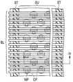
如图3所示,存储单元阵列10在沿着X轴的单元区域C1的一边设置有阶梯区域C2,在沿着Y轴的单元区域C1的一边设置有阶梯区域C3,在沿着Y轴的单元区域C1的另一边设置有虚设阶梯区域C4。As shown in FIG. 3 , the
<1-1-3-2>单元区域<1-1-3-2> Unit area
使用图4~图6对实施方式中的单元区域C1的结构进行说明。The structure of the cell region C1 in the embodiment will be described with reference to FIGS. 4 to 6 .
此外,在以下参照的附图中,Y方向是字线WL的延伸方向。X方向是位线BL的延伸方向。Z方向是相对于形成半导体存储装置1的半导体基板表面的垂直方向。In addition, in the drawings referred to below, the Y direction is the extending direction of the word line WL. The X direction is the extending direction of the bit line BL. The Z direction is a vertical direction with respect to the surface of the semiconductor substrate on which the
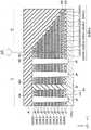
图4是表示图3的C即单元区域C1的布局的俯视图。FIG. 4 is a plan view showing the layout of the cell region C1 shown as C in FIG. 3 .
单元区域C1是形成与NAND字符串NS相对应的存储器柱MP的区域。The cell area C1 is an area in which the memory pillar MP corresponding to the NAND string NS is formed.
如图4所示,在形成单元区域C1的区域中例如包含多个狭缝ST、多个字符串单元SU和多个位线BL。As shown in FIG. 4 , the region in which the cell region C1 is formed includes, for example, a plurality of slits ST, a plurality of string cells SU, and a plurality of bit lines BL.
多个狭缝ST分别沿Y方向延伸、沿X方向排列。沿X方向相邻的狭缝ST之间例如配置一个字符串单元SU。The plurality of slits ST respectively extend in the Y direction and are arranged in the X direction. For example, one string unit SU is arranged between the slits ST adjacent in the X direction.
各字符串单元SU包含多个存储器柱MP。多个存储器柱MP例如沿着X方向配置成交错状。各存储器柱MP例如作为一个NAND字符串NS发挥功能。Each string unit SU includes a plurality of memory pillars MP. The plurality of memory pillars MP are arranged in a zigzag pattern along the X direction, for example. Each memory pillar MP functions as, for example, one NAND string NS.
多个位线BL分别沿Y方向延伸、沿X方向排列。例如,各位线BL以每个字符串单元SU与至少一个存储器柱MP重叠的方式进行配置。具体来说,在各存储器柱MP处例如重叠有两根位线BL。The plurality of bit lines BL respectively extend in the Y direction and are arranged in the X direction. For example, the bit lines BL are arranged such that each string unit SU overlaps with at least one memory pillar MP. Specifically, for example, two bit lines BL overlap each of the memory pillars MP.
在重叠于存储器柱MP的多个位线BL之中一根位线BL与该存储器柱MP之间设置了接触插塞CP。各存储器柱MP隔着接触插塞CP与相对应的位线BL电连接。A contact plug CP is provided between one bit line BL among the plurality of bit lines BL overlapping the memory column MP and the memory column MP. Each of the memory pillars MP is electrically connected to the corresponding bit line BL via the contact plug CP.
此外,设置于相邻狭缝ST之间的字符串单元SU的个数可以设定为任意的个数。图4所示的存储器柱MP的个数及配置只是一个例子,存储器柱MP可以设计为任意的个数及配置。与各存储器柱MP重叠的位线BL的根数可以设计为任意的根数。In addition, the number of the character string units SU provided between the adjacent slits ST can be set to an arbitrary number. The number and arrangement of the memory pillars MP shown in FIG. 4 are just an example, and the memory pillars MP can be designed in any number and arrangement. The number of bit lines BL overlapping each of the memory pillars MP can be designed to be an arbitrary number.
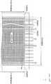
图5是沿着图4的IV-IV线的剖视图,其示出了实施方式的半导体存储装置1所具备的单元区域C1的结构。FIG. 5 is a cross-sectional view taken along the line IV-IV of FIG. 4 , and shows the structure of the cell region C1 included in the
如图5所示,在形成单元区域C1的区域中例如包含导体层21~25、存储器柱MP、接触插塞CP以及狭缝ST。As shown in FIG. 5 , the region in which the cell region C1 is formed includes, for example, conductor layers 21 to 25 , memory pillars MP, contact plugs CP, and slits ST.
具体来说,在半导体基板(未图示)的上方设置有导体层21。例如,导体层21形成为沿着XY平面扩展的板状,作为源极线使用。导体层21例如包含硅(Si)。Specifically, the
在导体层21的上方隔着绝缘膜41设置有导体层22。例如,导体层22形成为沿着XY平面扩展的板状,作为选择栅极线SGS使用。导体层22例如包含硅(Si)。The
在导体层22的上方隔着绝缘膜42交替层叠有导体层23和绝缘膜43。例如,导体层23形成为沿着XY平面扩展的板状。所层叠的多个导体层23从半导体基板20侧依次分别作为字线WL0~WL7使用。导体层23例如包含钨(W)。Conductor layers 23 and insulating
在最上层的导体层23的上方隔着绝缘膜44设置导体层24。导体层24例如形成为沿着XY平面扩展的板状,并且作为选择栅极线SGD使用。导体层24例如包含钨(W)。The
在导体层24的上方隔着绝缘膜45设置导体层25。例如,导体层25形成为沿着X方向延伸的线状,作为位线BL使用。即,在未图示的区域中多个导体层25沿着Y方向排列。导体层25例如包含铜(Cu)。The
存储器柱MP形成为沿着Z方向延伸的柱状,例如贯通导体层22~24。具体来说,存储器柱MP的上端例如包含于设置有导体层24的层与设置有导体层25的层之间的层。存储器柱MP的下端例如包含于设置有导体层21的层。The memory pillar MP is formed in a pillar shape extending in the Z direction, for example, penetrating the conductor layers 22 to 24 . Specifically, the upper end of the memory pillar MP is included in, for example, a layer between the layer in which the
此外,绝缘膜41~45例如包含氧化硅(SiO2)。Further, the insulating
如图6所示,存储器柱MP例如包含芯部件30、半导体层31及层叠膜32。As shown in FIG. 6 , the memory pillar MP includes, for example, a
芯部件30形成为沿着Z方向延伸的柱状。芯部件30的上端例如包含于比设置有导体层24的层更上层。芯部件30的下端例如包含于设置有导体层21的层。芯部件30例如包含氧化硅(SiO2)之类的绝缘体。The
芯部件30被半导体层31覆盖。半导体层31例如隔着存储器柱MP的侧面与作为导体层21一部分的导体层54相接触。半导体层31例如为多晶硅(Si)。就层叠膜32来说,除了导体层21与半导体层31相接触的部分之外覆盖半导体层31的侧面及底面。The
在包含导体层23的层中,芯部件30设置于存储器柱MP的中央部。半导体层31包围芯部件30的侧面。层叠膜32包围半导体层31的侧面。层叠膜32例如包含隧道绝缘膜33、绝缘膜34及区块绝缘膜35。In the layer including the
隧道绝缘膜33覆盖半导体层31的侧面。绝缘膜34包围隧道绝缘膜33的侧面。区块绝缘膜35包围绝缘膜34的侧面。导体层23包围区块绝缘膜35的侧面。The
隧道绝缘膜33例如包含氧化硅(SiO2)。绝缘膜34例如包含氮化硅(SiN)。区块绝缘膜35例如包含氧化硅(SiO2)。The
返回至图4,在半导体层31上设置有柱状的接触插塞CP。就图示的区域来说,示出了与两根存储器柱MP之中的一根存储器柱MP相对应的接触插塞CP。该区域中未连接接触插塞CP的存储器柱MP在未图示的区域中与接触插塞CP连接。Returning to FIG. 4 , columnar contact plugs CP are provided on the
一个导体层25即一根位线BL与接触插塞CP的上表面接触。在存储器柱MP与导体层25之间还可以隔着两个以上的接触插塞电连接,也可以隔着其它布线电连接。One
狭缝ST形成为沿着Z方向延伸的板状,例如分割导体层22~24。具体来说,狭缝ST的上端例如包含于包含存储器柱MP上端的层与设置有导体层25的层之间的层。The slit ST is formed in a plate shape extending in the Z direction, for example, dividing the conductor layers 22 to 24 . Specifically, the upper end of the slit ST is included, for example, in the layer between the layer including the upper end of the memory pillar MP and the layer in which the
在狭缝ST的内部设置有绝缘体。该绝缘体例如包含氧化硅(SiO2)之类的绝缘体。此外,狭缝ST内可以由多个种类的绝缘体构成。例如,可以在狭缝ST埋入氧化硅之前形成作为狭缝ST的侧壁的氮化硅(SiN)。An insulator is provided inside the slit ST. The insulator includes, for example, an insulator such as silicon oxide (SiO2 ). In addition, the inside of the slit ST may be composed of a plurality of types of insulators. For example, silicon nitride (SiN), which is a sidewall of the slit ST, may be formed before the slit ST is buried in silicon oxide.
就以上进行了说明的存储器柱MP的构成来说,例如存储器柱MP与导体层22交叉的部分作为选择晶体管ST2发挥功能。存储器柱MP与导体层23交叉的部分作为存储器单元晶体管MT发挥功能。存储器柱MP与导体层24交叉的部分作为选择晶体管ST1发挥功能。Regarding the configuration of the memory column MP described above, for example, the portion where the memory column MP intersects with the
即,半导体层31作为存储器单元晶体管MT以及选择晶体管ST1及ST2的各自的沟道使用。绝缘膜34作为存储器单元晶体管MT的电荷储存层使用。That is, the
此外,就以上进行了说明的存储单元阵列10的结构来说,导体层23的个数基于字线WL的根数进行设计。设置成多个层的多个导体层24可以分配至选择栅极线SGD。设置成多个层的多个导体层22也可以分配至选择栅极线SGS。当选择栅极线SGS设置成多个层时,还可以使用与导体层22不同的导体。In addition, in the structure of the
<1-1-3-3>阶梯区域<1-1-3-3> Step area
使用图7,对实施方式的阶梯区域C2的结构进行说明。The structure of the stepped region C2 of the embodiment will be described with reference to FIG. 7 .
图7是图3的A-A’剖面即阶梯区域C2的剖面。阶梯区域C2是与选择栅极线SGD及SGS以及字线WL0~WL7相对应的多个导体层22~24以阶梯状被引出的区域(以下将引出部称为“阶台”或“突出部”)。在各阶台上形成有接触插塞CC。接触插塞CC隔着设置于上端的布线层(未图示)与行解码器模块15连接。接触插塞CC由导电材料构成,例如可以使用钨(W)或氮化钛(TiN)之类的金属材料。Fig. 7 is a cross-section of the stepped region C2 taken along the line A-A' in Fig. 3 . The stepped region C2 is a region in which the plurality of conductor layers 22 to 24 corresponding to the select gate lines SGD and SGS and the word lines WL0 to WL7 are drawn out in a stepped shape (the lead-out portion is hereinafter referred to as a "step" or "protrusion"). ”). A contact plug CC is formed on each step. The contact plug CC is connected to the
具体来说,如图7所示,选择栅极线SGS在单元区域C1中使用导体层22,在阶梯区域C2中设置导体层122。进而,导体层22和导体层122与单元区域C1和阶梯区域C2的边界连接。该导体层122作为选择栅极线SGS的阶台发挥功能,并且与沿Z轴方向延伸的接触插塞CC连接。该导体层122例如包含多晶硅。Specifically, as shown in FIG. 7, the selection gate line SGS uses the
另外,字线WL0~WL7在单元区域C1中使用导体层23,在阶梯区域C2中设置导体层123。而且,导体层23和导体层123与单元区域C1和阶梯区域C2的边界连接。该导体层123作为字线WL0~WL7的阶台发挥功能,与沿Z轴方向延伸的接触插塞CC连接。该导体层123例如包含多晶硅。另外,导体层123还可以包含杂质(例如钨)。In addition, the word lines WL0 to WL7 use the
另外,选择栅极线SGD在单元区域C1中使用导体层24,在阶梯区域C2中设置有导体层124。而且,导体层24和导体层124与单元区域C1和阶梯区域C2的边界连接。该导体层124作为选择栅极线SGD的阶台发挥功能,并且与沿Z轴方向延伸的接触插塞CC连接。该导体层124例如包含多晶硅。In addition, the selection gate line SGD uses the
此外,将设置于单元区域C1的绝缘膜41~44分别标记为绝缘膜41A~44A,将设置于阶梯区域C2的绝缘膜41~44分别标记为绝缘膜41B~44B。In addition, the insulating
<1-1-3-4>虚设阶梯区域<1-1-3-4> Dummy staircase area
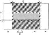
使用图8,对实施方式中的虚设阶梯区域C4的结构进行说明。The structure of the dummy stepped region C4 in the embodiment will be described with reference to FIG. 8 .
图8是图3的B-B’剖面即虚设阶梯区域C4的剖面。虚设阶梯区域C4是将与选择栅极线SGD及SGS以及字线WL0~WL7相对应的多个导体层22~24以阶梯状引出的区域。将虚设阶梯区域C4中的被引出的区域记载为虚设阶台等。作为在阶梯区域C2和虚设阶梯区域C4中不同的部分,在各虚设阶台不设置接触插塞CC。Fig. 8 is a cross section of the dummy stepped region C4 taken along the line B-B' in Fig. 3 . The dummy stepped region C4 is a region in which the plurality of conductor layers 22 to 24 corresponding to the select gate lines SGD and SGS and the word lines WL0 to WL7 are drawn out in a stepped shape. The extracted area in the dummy step area C4 is described as a dummy step or the like. The contact plugs CC are not provided in the respective dummy steps as the difference between the step area C2 and the dummy step area C4.
具体来说,如图8所示,选择栅极线SGS在单元区域C1中使用导体层22,在虚设阶梯区域C4中设置有导体层222。而且,导体层22和导体层222与单元区域C1和虚设阶梯区域C4的边界连接。该导体层222作为选择栅极线SGS的虚设阶台发挥功能,例如包含多晶硅。Specifically, as shown in FIG. 8 , the selection gate line SGS uses the
另外,字线WL0~WL7在单元区域C1中使用导体层23,在虚设阶梯区域C4中设置导体层223。而且,导体层23和导体层223与单元区域C1和虚设阶梯区域C4的边界连接。该导体层223作为字线WL0~WL7的虚设阶台发挥功能,例如包含多晶硅。In addition, the word lines WL0 to WL7 use the
另外,选择栅极线SGD在单元区域C1中使用导体层24,在虚设阶梯区域C4中设置导体层224。而且,导体层24和导体层224与单元区域C1和虚设阶梯区域C4的边界连接。该导体层224作为选择栅极线SGD的虚设阶台发挥功能,例如包含多晶硅。In addition, the selection gate line SGD uses the
此外,将设置于虚设阶梯区域C4的绝缘膜41~44分别标记为绝缘膜41B~44B。In addition, the insulating
此外,以上情况在其它虚设阶梯区域C3也是相同的。In addition, the above is also the same in the other dummy step regions C3.
<1-1-3-5>字线<1-1-3-5> Word line
在此,使用图9对设置于单元区域C1、阶梯区域C2、虚设阶梯区域C3及C4的字线WL6进行说明。Here, the word line WL6 provided in the cell region C1 , the step region C2 , and the dummy step regions C3 and C4 will be described with reference to FIG. 9 .
如图9所示,字线WL6为板状的导体层,其以跨越单元区域C1、阶梯区域C2、虚设阶梯区域C3及C4的方式进行设置。将位于单元区域C1的字线WL6标记为23,将位于阶梯区域C2的字线WL6标记为123,将位于虚设阶梯区域C3及C4的字线WL6标记为223。As shown in FIG. 9 , the word line WL6 is a plate-shaped conductor layer, which is provided so as to straddle the cell region C1 , the step region C2 , and the dummy step regions C3 and C4 . The word line WL6 located in the cell region C1 is marked as 23, the word line WL6 located in the step region C2 is marked as 123, and the word line WL6 located in the dummy stepped regions C3 and C4 is marked as 223.
<1-2>半导体存储装置1的制造方法<1-2> Manufacturing method of
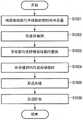
以下,适当参照图10对实施方式的半导体存储装置1中的从形成与字线相对应的层叠结构至形成狭缝ST的一系列制造工序进行说明。图10是表示实施方式的半导体存储装置1的制造方法的流程图。图11~图16分别示出了实施方式的半导体存储装置1的制造工序中的包含与单元区域C1及虚设阶梯区域C4相对应的结构体的结构。Hereinafter, a series of manufacturing steps from the formation of the stacked structure corresponding to the word line to the formation of the slit ST in the
[步骤S1001][Step S1001]
在未图示的半导体基板的上方层叠源极线部和字线部的牺牲部件。具体来说,如图11所示,在未图示的半导体基板的上方形成导体层21。在导体层21上交替层叠绝缘体层321及牺牲部件322。The sacrificial members of the source line portion and the word line portion are stacked on a semiconductor substrate (not shown). Specifically, as shown in FIG. 11 , a
导体层21为源极线部。导体层21例如包含多晶硅(Si)。绝缘体层321例如包含氧化硅(SiO2)。绝缘体层321的膜厚例如为15nm以下。将各牺牲部件322置换成选择栅极线及字线部。例如,形成牺牲部件322的层数与层叠的选择栅极线及字线WL的根数相对应。牺牲部件322例如包含多晶硅。The
[步骤S1002][Step S1002]
接着,形成存储洞MH。具体来说,首先通过光刻法等形成与存储洞MH相对应的区域开口后的掩模(未图示)。然后,如图12所示,通过使用了所形成的掩模的各向异性蚀刻,形成存储洞MH。Next, memory holes MH are formed. Specifically, first, a mask (not shown) in which regions corresponding to the memory holes MH are opened is formed by photolithography or the like. Then, as shown in FIG. 12 , memory holes MH are formed by anisotropic etching using the formed mask.
由本工序形成的存储洞MH分别贯通绝缘体层321及牺牲部件322,存储洞MH的底部例如在导体层21内停止。本工序中的各向异性蚀刻例如为RIE(反应离子蚀刻;ReactiveIon Etching)。The memory holes MH formed in this step pass through the
[步骤S1003][Step S1003]
接着,执行字线部与选择栅极线部的置换处理。具体来说,如图13所示,将在存储洞MH内露出的牺牲部件322暴露于氟化钨(WF6)气体。由此,将在存储洞MH内露出的牺牲部件322的多晶硅置换成钨(W)。由此,形成分别与字线WL0~WL7相对应的多个导体层23及与选择栅极线SGS、SGD相对应的导体层22、24。此外,将导体层22~24置换成钨(W),但有时硅(Si)以杂质水平残留。Next, the replacement process of the word line portion and the select gate line portion is performed. Specifically, as shown in FIG. 13 , the
此外,虚设阶梯区域C4中的牺牲部件322由于氟化钨(WF6)气体不会达到,因此不会被置换成钨(W),多晶硅残留。In addition, since the
[步骤S1004][Step S1004]
在存储洞MH内形成存储器柱MP。具体来说,如图14所示,在存储洞MH的侧面及底面形成区块绝缘膜35(氧化硅(SiO2)),在区块绝缘膜35上形成作为绝缘膜34的氮化硅,在绝缘膜34上形成作为隧道绝缘膜33的氧化硅(SiO2),在隧道绝缘膜33上形成作为半导体层31的硅(Si),在半导体层31上形成作为芯部件30的绝缘材料。如此,在存储洞MH内形成存储器柱MP。A memory pillar MP is formed within the memory hole MH. Specifically, as shown in FIG. 14 , a block insulating film 35 (silicon oxide (SiO2 )) is formed on the side and bottom surfaces of the memory hole MH, and silicon nitride as the insulating
[步骤S1005][Step S1005]
接着,形成狭缝ST。具体来说,首先通过光刻法等形成与狭缝ST相对应的区域开口后的掩模(未图示)。然后,如图15所示,通过使用了所形成的掩模的各向异性蚀刻,形成狭缝ST。Next, the slit ST is formed. Specifically, first, a mask (not shown) in which a region corresponding to the slit ST is opened is formed by photolithography or the like. Then, as shown in FIG. 15 , the slit ST is formed by anisotropic etching using the formed mask.
由本工序形成的狭缝ST分别分割绝缘体层321、导体层22~24,狭缝ST的底部例如在设置有导体层21的层内停止。本工序中的各向异性蚀刻例如为RIE。The slit ST formed in this step divides the insulating
而且,之后通过绝缘体26填埋狭缝ST内。之后,例如通过CMP将形成于狭缝ST外的绝缘体26去除。其结果是形成狭缝ST被绝缘体26填埋而成的结构。绝缘体26例如包含氧化硅(SiO2)。Then, the inside of the slit ST is filled with the
[步骤S1006][Step S1006]
接着,形成虚设阶台(阶台)。如图16所示,依次通过各向异性蚀刻等以阶梯状将导体层及绝缘膜的组去除而形成虚设阶台222~224。Next, a dummy step (step) is formed. As shown in FIG. 16 , dummy steps 222 to 224 are formed by sequentially removing the conductor layer and the insulating film group in a stepped shape by anisotropic etching or the like.
通过以上进行了说明的实施方式的半导体存储装置1的制造工序,分别形成存储器柱MP、与存储器柱MP连接的源极线SL、字线WL以及选择栅极线SGS及SGD。此外,以上进行了说明的制造工序仅为一个例子,可以在各制造工序之间插入其它的处理,也可以在没有问题的范围内改变制造工序的顺序。Through the manufacturing process of the
另外,以上阐述了虚设阶梯区域C4,对于阶梯区域C2及虚设阶梯区域C3也与虚设阶梯区域C4相同地形成。In addition, the dummy stepped region C4 has been described above, but the stepped region C2 and the dummy stepped region C3 are also formed in the same manner as the dummy stepped region C4.
<1-3>实施方式的效果<1-3> Effects of Embodiment
根据上述实施方式,作为层叠结构(选择栅极线及字线)的形成方法,将氧化硅(SiO2)和多晶硅交替地层叠多层,形成存储洞MH。之后,将在存储洞MH内露出的多晶硅暴露于氟化钨(WF6)气体。由此,将作为选择栅极线及字线发挥功能的多晶硅置换成钨(W)。According to the above-described embodiment, as a method of forming the stacked structure (selection gate lines and word lines), silicon oxide (SiO2 ) and polysilicon are alternately stacked in multiple layers to form memory holes MH. After that, the polysilicon exposed in the memory hole MH is exposed to tungsten fluoride (WF6 ) gas. As a result, the polysilicon that functions as the select gate line and the word line is replaced with tungsten (W).
由此,能够减少狭缝ST的数量、阶梯区域及虚设阶梯区域中的支撑部件,并且能够缩短Z方向中的钨之间的距离。Thereby, the number of slits ST, the support members in the stepped region and the dummy stepped region can be reduced, and the distance between tungsten in the Z direction can be shortened.
以下,为了对实施方式的效果进行说明,简单地对比较例进行说明。Hereinafter, in order to explain the effect of the embodiment, a comparative example will be briefly described.
以下,适当参照图17,对于比较例的半导体存储装置1中的与字线相对应的层叠结构的形成至阶梯的形成的一系列制造工序进行说明。图17是表示比较例的半导体存储装置1的制造方法的流程图。图18~图23分别表示比较例的半导体存储装置1的制造工序中的包含与单元区域C1及虚设阶梯区域C4相对应的结构体的结构。Hereinafter, with reference to FIG. 17 as appropriate, a series of manufacturing steps from the formation of the stacked structure corresponding to the word lines to the formation of the steps in the
[步骤S2001][Step S2001]
在半导体基板的上方层叠源极线部和字线部的牺牲部件。具体来说,如图18所示,在未图示的半导体基板的上方形成导体层21。在导体层21上交替层叠绝缘体层421及牺牲部件422。The sacrificial members of the source line portion and the word line portion are stacked above the semiconductor substrate. Specifically, as shown in FIG. 18 , a
绝缘体层421例如包含氧化硅(SiO2)。各牺牲部件422例如包含氮化硅(SiN)。The
[步骤S2002][Step S2002]
接着,如图19所示,形成存储器柱MP及支撑部HR。就该支撑部HR来说,在后段去除牺牲部件422时,其是用于以未形成存储器柱MP的阶梯区域不会崩溃的方式进行支撑的结构。该支撑部HR例如是沿Z轴方向延伸的柱状的绝缘体。另外,该支撑部HR也可以不在本实施方式中设置。Next, as shown in FIG. 19 , the memory pillar MP and the support portion HR are formed. This support portion HR is a structure for supporting so that the stepped region where the memory pillar MP is not formed does not collapse when the
[步骤S2003][Step S2003]
接着,如图20所示,形成狭缝ST。Next, as shown in FIG. 20 , the slit ST is formed.
[步骤S2004][Step S2004]
接着,如图21所示,隔着狭缝ST例如进行基于热磷酸的湿式蚀刻。由此,将牺牲部件422选择性去除。去除了牺牲部件422的结构体通过多个存储器柱MP及多个支撑部HR等维持其立体结构。Next, as shown in FIG. 21 , wet etching by, for example, hot phosphoric acid is performed through the slit ST. Thus, the
[步骤S2005][Step S2005]
接着,执行字线部与选择栅极线部的置换处理。具体来说,如图22及图23所示,例如通过CVD,在去除了牺牲部件422的空间成膜了作为阻挡金属的氮化钛(TiN)423,然后形成钨(W)424。由此,形成分别与字线WL0~WL7相对应的多个导体层23和与选择栅极线SGD相对应的导体层24。Next, the replacement process of the word line portion and the select gate line portion is performed. Specifically, as shown in FIGS. 22 and 23 , titanium nitride (TiN) 423 as a barrier metal is formed in the space where the
然后,使用氟化钨(WF6)气体形成钨(W)424。但是,该氟化钨(WF6)气体所包含的氟(F)有时会对存储器柱MP造成不良影响。因此,与本实施方式不同,就比较例来说有必要设置作为阻挡金属的氮化钛(TiN)423。Then, tungsten (W) 424 is formed using tungsten fluoride (WF6 ) gas. However, fluorine (F) contained in the tungsten fluoride (WF6 ) gas may adversely affect the memory column MP. Therefore, unlike the present embodiment, it is necessary to provide titanium nitride (TiN) 423 as a barrier metal in the comparative example.
该氮化钛(TiN)的膜厚为d1(例如3nm左右)。The film thickness of this titanium nitride (TiN) is d1 (for example, about 3 nm).
之后,通过任意的制造工序形成半导体存储装置。After that, a semiconductor memory device is formed by an arbitrary manufacturing process.
如上所述,就比较例来说,当作为层叠结构(选择栅极线及字线)将氧化硅(SiO2)与氮化硅(SiN)交替地层叠多层而形成狭缝时,将氮化硅(SiN)去除,填埋作为选择栅极线及字线的部件的阻挡金属和导电材料,由此形成半导体存储装置。As described above, in the comparative example, when a plurality of layers of silicon oxide (SiO2 ) and silicon nitride (SiN) are alternately stacked as a stacked structure (selection gate line and word line) to form a slit, nitrogen Silicon oxide (SiN) is removed to fill the barrier metal and conductive material that are components of the select gate lines and word lines, thereby forming a semiconductor memory device.
但是,如在比较例进行了说明的那样,在去除牺牲部件422时,为了维持立体结构,支撑部HR变得必要。另外,为了使用于去除牺牲部件422的蚀刻溶液遍布,与本实施方式相比,需要更多的狭缝ST。另外,就比较例来说,在形成了存储器柱之后,形成作为选择栅极线及字线的钨(W)。因此,需要用于由在形成钨(W)时的氟化钨(WF6)气体的氟保护存储器柱MP(F)的阻挡金属。However, as described in the comparative example, when the
另一方面,根据上述实施方式,不会如比较例的步骤S2004那样将牺牲部件去除。因此,用于支撑立体结构的支撑部HR变得不需要。其结果是,本实施方式与比较例相比能够减少支撑部HR部分的面积。换言之,本实施方式的阶梯区域中,沿Z方向延伸的柱状体可以说全部是接触插塞。另外,在虚设阶梯区域中,未设置沿Z方向延伸的柱状体。另外,根据上述实施方式,不需要使用于去除牺牲部件422的蚀刻溶液遍布。其结果是,本实施方式与比较例相比能够抑制狭缝ST的数量,能够仅减少狭缝数量的面积。另外,根据上述实施方式,与比较例不同,在形成选择栅极线及字线之后,形成存储器柱MP。虽然形成存储器柱MP,但由于未暴露于氟化钨(WF6)气体,因此比较例中进行了说明的设置于选择栅极线及字线的阻挡金属变得不需要。具体来说,未在选择栅极线及字线与于Z方向相邻的绝缘膜之间以及存储器柱与选择栅极线及字线之间设置阻挡金属。其结果是,就本实施方式来说,对于各个选择栅极线及字线,就Z轴方向、X轴及Y轴方向来说能够分别仅减小d1×2(阻挡金属的厚度约为3nm时为6nm)的面积。通过使绝缘膜的膜厚变薄,能够降低字线电阻。如上所述,根据上述实施方式,与比较例相比能够减小半导体存储装置的尺寸。On the other hand, according to the above-described embodiment, the sacrificial member is not removed as in step S2004 of the comparative example. Therefore, the support portion HR for supporting the three-dimensional structure becomes unnecessary. As a result, this embodiment can reduce the area of the support part HR part compared with a comparative example. In other words, in the stepped region of the present embodiment, all the columnar bodies extending in the Z direction can be said to be contact plugs. In addition, in the dummy stepped region, no columnar body extending in the Z direction is provided. In addition, according to the above-described embodiment, it is not necessary to spread the etching solution for removing the
<2>其它变形例等<2> Other modifications, etc.
上述实施方式及变形例中进行了说明的制造工序仅为一个例子,也可以在各制造工序之间插入其它的处理,还可以适当地替换制造工序。半导体存储装置1的制造工序只要是能够形成在上述实施方式及变形例中进行了说明的结构,就可以适用任何制造工序。The manufacturing steps described in the above-described embodiments and modifications are merely examples, and other processes may be inserted between the respective manufacturing steps, and the manufacturing steps may be appropriately replaced. Any manufacturing process can be applied to the manufacturing process of the
就上述实施方式来说,存储单元阵列10的结构也可以是其它结构。例如,存储器柱MP可以是多个柱体沿Z方向连接的结构。例如,存储器柱MP可以是贯通导体层24(选择栅极线SGD)的柱体与贯通多个导体层23(字线WL)的柱体相连接的结构。另外,存储器柱MP还可以分别是贯通多个导体层23的多个柱体沿Z方向连接而成的结构。As for the above-mentioned embodiment, the structure of the
本说明书中,“多晶硅”也可以称为多晶的半导体。In this specification, "polysilicon" may also be referred to as a polycrystalline semiconductor.
对本发明的数个实施方式进行了说明,但这些实施方式是作为例子呈现的,并不旨在对发明范围进行限定。这些新的实施方式可以以其它各种方式进行实施,在不脱离发明主旨的范围可以进行各种省略、替换、变更。这些实施方式、其变形包含于发明范围或主旨并且包含于权利要求书所记载的发明及与其等同的范围。Several embodiments of the present invention have been described, but these embodiments are presented as examples and are not intended to limit the scope of the invention. These novel embodiments can be implemented in various other forms, and various omissions, substitutions, and changes can be made without departing from the gist of the invention. These embodiments and modifications thereof are included in the scope and spirit of the invention, and are included in the invention described in the claims and the scope equivalent thereto.
Claims (8)
Applications Claiming Priority (1)
| Application Number | Priority Date | Filing Date | Title |
|---|---|---|---|
| PCT/JP2020/024598WO2021260792A1 (en) | 2020-06-23 | 2020-06-23 | Semiconductor storage device |
Publications (1)
| Publication Number | Publication Date |
|---|---|
| CN115053341Atrue CN115053341A (en) | 2022-09-13 |
Family
ID=79031447
Family Applications (1)
| Application Number | Title | Priority Date | Filing Date |
|---|---|---|---|
| CN202080008618.6APendingCN115053341A (en) | 2020-06-23 | 2020-06-23 | Semiconductor memory device with a plurality of memory cells |
Country Status (3)
| Country | Link |
|---|---|
| US (1) | US12327787B2 (en) |
| CN (1) | CN115053341A (en) |
| WO (1) | WO2021260792A1 (en) |
Citations (3)
| Publication number | Priority date | Publication date | Assignee | Title |
|---|---|---|---|---|
| CN106024786A (en)* | 2015-03-31 | 2016-10-12 | 三星电子株式会社 | Three-dimensional semiconductor device |
| US20200051989A1 (en)* | 2018-08-10 | 2020-02-13 | Toshiba Memory Corporation | Semiconductor device |
| CN110931496A (en)* | 2018-09-20 | 2020-03-27 | 东芝存储器株式会社 | Semiconductor memory device with a plurality of memory cells |
Family Cites Families (10)
| Publication number | Priority date | Publication date | Assignee | Title |
|---|---|---|---|---|
| JP4056588B2 (en) | 1996-11-06 | 2008-03-05 | 富士通株式会社 | Semiconductor device and manufacturing method thereof |
| JP5016928B2 (en) | 2007-01-10 | 2012-09-05 | 株式会社東芝 | Nonvolatile semiconductor memory device and manufacturing method thereof |
| JP2010027870A (en) | 2008-07-18 | 2010-02-04 | Toshiba Corp | Semiconductor memory and manufacturing method thereof |
| JP5593283B2 (en) | 2011-08-04 | 2014-09-17 | 株式会社東芝 | Semiconductor memory device and manufacturing method thereof |
| JP2015056452A (en)* | 2013-09-10 | 2015-03-23 | 株式会社東芝 | Semiconductor memory device and manufacturing method thereof |
| KR20150089138A (en)* | 2014-01-27 | 2015-08-05 | 삼성전자주식회사 | Vertical non-volatile memory devices and methods of manufacturing the same |
| JP2018046167A (en)* | 2016-09-15 | 2018-03-22 | 株式会社東芝 | Semiconductor memory device and method for manufacturing the same |
| KR102443047B1 (en)* | 2017-11-16 | 2022-09-14 | 에이에스엠 아이피 홀딩 비.브이. | Method of processing a substrate and a device manufactured by the same |
| JP2020145233A (en)* | 2019-03-04 | 2020-09-10 | キオクシア株式会社 | Semiconductor device and manufacturing method thereof |
| US10804197B1 (en)* | 2019-03-28 | 2020-10-13 | Sandisk Technologies Llc | Memory die containing stress reducing backside contact via structures and method of making the same |
- 2020
- 2020-06-23CNCN202080008618.6Apatent/CN115053341A/enactivePending
- 2020-06-23WOPCT/JP2020/024598patent/WO2021260792A1/ennot_activeCeased
- 2021
- 2021-09-10USUS17/447,332patent/US12327787B2/enactiveActive
Patent Citations (3)
| Publication number | Priority date | Publication date | Assignee | Title |
|---|---|---|---|---|
| CN106024786A (en)* | 2015-03-31 | 2016-10-12 | 三星电子株式会社 | Three-dimensional semiconductor device |
| US20200051989A1 (en)* | 2018-08-10 | 2020-02-13 | Toshiba Memory Corporation | Semiconductor device |
| CN110931496A (en)* | 2018-09-20 | 2020-03-27 | 东芝存储器株式会社 | Semiconductor memory device with a plurality of memory cells |
Also Published As
| Publication number | Publication date |
|---|---|
| WO2021260792A1 (en) | 2021-12-30 |
| US12327787B2 (en) | 2025-06-10 |
| US20210407905A1 (en) | 2021-12-30 |
Similar Documents
| Publication | Publication Date | Title |
|---|---|---|
| TWI707458B (en) | Semiconductor memory device | |
| US20220173032A1 (en) | Semiconductor memory device | |
| CN110858592B (en) | Semiconductor memory and method for manufacturing semiconductor memory | |
| JP2020107673A (en) | Semiconductor storage device | |
| TWI718588B (en) | Semiconductor memory device and manufacturing method thereof | |
| CN111599821B (en) | Semiconductor memory device and method for manufacturing the same | |
| CN111739889B (en) | Semiconductor memory device with a memory cell having a memory cell with a memory cell having a memory cell | |
| CN111696999A (en) | Semiconductor memory device with a plurality of memory cells | |
| TWI671890B (en) | Semiconductor memory | |
| CN112420726B (en) | Semiconductor memory device with a memory cell having a memory cell with a memory cell having a memory cell | |
| TWI714211B (en) | Semiconductor memory device | |
| CN110931496B (en) | Semiconductor memory device with a memory cell having a memory cell with a memory cell having a memory cell | |
| CN112530970B (en) | Semiconductor memory device with a memory cell having a memory cell with a memory cell having a memory cell | |
| TWI689021B (en) | Semiconductor device | |
| KR20220021181A (en) | Nonvolatile memory device including erase transistor | |
| JP2020161672A (en) | Semiconductor storage device | |
| TW202315080A (en) | Semiconductor memory device and method of manufacturing the semiconductor memory device | |
| CN115053341A (en) | Semiconductor memory device with a plurality of memory cells | |
| US20250095737A1 (en) | Memory device | |
| US20250210366A1 (en) | Manufacturing method of semiconductor device | |
| US20230309303A1 (en) | Semiconductor memory device and method for manufacturing semiconductor memory device | |
| JP2023043646A (en) | memory device | |
| CN116801630A (en) | Semiconductor memory device |
Legal Events
| Date | Code | Title | Description |
|---|---|---|---|
| PB01 | Publication | ||
| PB01 | Publication | ||
| SE01 | Entry into force of request for substantive examination | ||
| SE01 | Entry into force of request for substantive examination |