CN115051573A - Switching power supply and method for use in a switching power supply - Google Patents
Switching power supply and method for use in a switching power supplyDownload PDFInfo
- Publication number
- CN115051573A CN115051573ACN202210648568.9ACN202210648568ACN115051573ACN 115051573 ACN115051573 ACN 115051573ACN 202210648568 ACN202210648568 ACN 202210648568ACN 115051573 ACN115051573 ACN 115051573A
- Authority
- CN
- China
- Prior art keywords
- chip
- power supply
- preset threshold
- switching power
- voltage
- Prior art date
- Legal status (The legal status is an assumption and is not a legal conclusion. Google has not performed a legal analysis and makes no representation as to the accuracy of the status listed.)
- Pending
Links
Images


Classifications
- H—ELECTRICITY
- H02—GENERATION; CONVERSION OR DISTRIBUTION OF ELECTRIC POWER
- H02M—APPARATUS FOR CONVERSION BETWEEN AC AND AC, BETWEEN AC AND DC, OR BETWEEN DC AND DC, AND FOR USE WITH MAINS OR SIMILAR POWER SUPPLY SYSTEMS; CONVERSION OF DC OR AC INPUT POWER INTO SURGE OUTPUT POWER; CONTROL OR REGULATION THEREOF
- H02M3/00—Conversion of DC power input into DC power output
- H02M3/22—Conversion of DC power input into DC power output with intermediate conversion into AC
- H02M3/24—Conversion of DC power input into DC power output with intermediate conversion into AC by static converters
- H02M3/28—Conversion of DC power input into DC power output with intermediate conversion into AC by static converters using discharge tubes with control electrode or semiconductor devices with control electrode to produce the intermediate AC
- H02M3/325—Conversion of DC power input into DC power output with intermediate conversion into AC by static converters using discharge tubes with control electrode or semiconductor devices with control electrode to produce the intermediate AC using devices of a triode or a transistor type requiring continuous application of a control signal
- H02M3/335—Conversion of DC power input into DC power output with intermediate conversion into AC by static converters using discharge tubes with control electrode or semiconductor devices with control electrode to produce the intermediate AC using devices of a triode or a transistor type requiring continuous application of a control signal using semiconductor devices only
- H02M3/33569—Conversion of DC power input into DC power output with intermediate conversion into AC by static converters using discharge tubes with control electrode or semiconductor devices with control electrode to produce the intermediate AC using devices of a triode or a transistor type requiring continuous application of a control signal using semiconductor devices only having several active switching elements
- H02M3/33576—Conversion of DC power input into DC power output with intermediate conversion into AC by static converters using discharge tubes with control electrode or semiconductor devices with control electrode to produce the intermediate AC using devices of a triode or a transistor type requiring continuous application of a control signal using semiconductor devices only having several active switching elements having at least one active switching element at the secondary side of an isolation transformer
- H02M3/33592—Conversion of DC power input into DC power output with intermediate conversion into AC by static converters using discharge tubes with control electrode or semiconductor devices with control electrode to produce the intermediate AC using devices of a triode or a transistor type requiring continuous application of a control signal using semiconductor devices only having several active switching elements having at least one active switching element at the secondary side of an isolation transformer having a synchronous rectifier circuit or a synchronous freewheeling circuit at the secondary side of an isolation transformer
- H—ELECTRICITY
- H02—GENERATION; CONVERSION OR DISTRIBUTION OF ELECTRIC POWER
- H02H—EMERGENCY PROTECTIVE CIRCUIT ARRANGEMENTS
- H02H5/00—Emergency protective circuit arrangements for automatic disconnection directly responsive to an undesired change from normal non-electric working conditions with or without subsequent reconnection
- H02H5/04—Emergency protective circuit arrangements for automatic disconnection directly responsive to an undesired change from normal non-electric working conditions with or without subsequent reconnection responsive to abnormal temperature
- H02H5/047—Emergency protective circuit arrangements for automatic disconnection directly responsive to an undesired change from normal non-electric working conditions with or without subsequent reconnection responsive to abnormal temperature using a temperature responsive switch
- H—ELECTRICITY
- H02—GENERATION; CONVERSION OR DISTRIBUTION OF ELECTRIC POWER
- H02H—EMERGENCY PROTECTIVE CIRCUIT ARRANGEMENTS
- H02H7/00—Emergency protective circuit arrangements specially adapted for specific types of electric machines or apparatus or for sectionalised protection of cable or line systems, and effecting automatic switching in the event of an undesired change from normal working conditions
- H02H7/10—Emergency protective circuit arrangements specially adapted for specific types of electric machines or apparatus or for sectionalised protection of cable or line systems, and effecting automatic switching in the event of an undesired change from normal working conditions for converters; for rectifiers
- H02H7/12—Emergency protective circuit arrangements specially adapted for specific types of electric machines or apparatus or for sectionalised protection of cable or line systems, and effecting automatic switching in the event of an undesired change from normal working conditions for converters; for rectifiers for static converters or rectifiers
- H02H7/1213—Emergency protective circuit arrangements specially adapted for specific types of electric machines or apparatus or for sectionalised protection of cable or line systems, and effecting automatic switching in the event of an undesired change from normal working conditions for converters; for rectifiers for static converters or rectifiers for DC-DC converters
- H—ELECTRICITY
- H02—GENERATION; CONVERSION OR DISTRIBUTION OF ELECTRIC POWER
- H02M—APPARATUS FOR CONVERSION BETWEEN AC AND AC, BETWEEN AC AND DC, OR BETWEEN DC AND DC, AND FOR USE WITH MAINS OR SIMILAR POWER SUPPLY SYSTEMS; CONVERSION OF DC OR AC INPUT POWER INTO SURGE OUTPUT POWER; CONTROL OR REGULATION THEREOF
- H02M1/00—Details of apparatus for conversion
- H02M1/36—Means for starting or stopping converters
- Y—GENERAL TAGGING OF NEW TECHNOLOGICAL DEVELOPMENTS; GENERAL TAGGING OF CROSS-SECTIONAL TECHNOLOGIES SPANNING OVER SEVERAL SECTIONS OF THE IPC; TECHNICAL SUBJECTS COVERED BY FORMER USPC CROSS-REFERENCE ART COLLECTIONS [XRACs] AND DIGESTS
- Y02—TECHNOLOGIES OR APPLICATIONS FOR MITIGATION OR ADAPTATION AGAINST CLIMATE CHANGE
- Y02B—CLIMATE CHANGE MITIGATION TECHNOLOGIES RELATED TO BUILDINGS, e.g. HOUSING, HOUSE APPLIANCES OR RELATED END-USER APPLICATIONS
- Y02B70/00—Technologies for an efficient end-user side electric power management and consumption
- Y02B70/10—Technologies improving the efficiency by using switched-mode power supplies [SMPS], i.e. efficient power electronics conversion e.g. power factor correction or reduction of losses in power supplies or efficient standby modes
Landscapes
- Engineering & Computer Science (AREA)
- Power Engineering (AREA)
- Dc-Dc Converters (AREA)
Abstract
Translated fromChinese
Description
Translated fromChinese技术领域technical field
本发明属于集成电路领域,尤其涉及一种开关电源和用在开关电源中的方法。The invention belongs to the field of integrated circuits, and in particular relates to a switching power supply and a method used in the switching power supply.
背景技术Background technique
在充电器或适配器中,采用同步整流,来控制超低导通电阻的MOSFET以代替二极管整流,能够有效地降低由输出整流二极管上的较高压降造成的损耗,可以提升系统的整体效率,这也是目前实现能效提高的一种简单、低成本的方式。In chargers or adapters, synchronous rectification is used to control ultra-low on-resistance MOSFETs instead of diode rectification, which can effectively reduce the loss caused by the higher voltage drop on the output rectifier diode and improve the overall efficiency of the system. It is also a simple and low-cost way to achieve energy efficiency improvement.
然而,传统开关电源的副边同步整流芯片无法检测自身温度,可能在温度过高时,导致副边开关管损坏或者可能发生熔壳等问题。However, the secondary-side synchronous rectifier chip of the traditional switching power supply cannot detect its own temperature, which may cause damage to the secondary-side switch tube or may cause problems such as fusion shell when the temperature is too high.
发明内容SUMMARY OF THE INVENTION
本发明实施例提供了一种开关电源和用在开关电源中的方法,可以利用副边同步整流芯片对其本体温度进行检测,并在检测到温度过高时向原边反馈芯片发送温度保护请求信息,使得原边反馈芯片进入自动重启状态,防止由于副边温度过高,导致副边开关管损坏或者发生熔壳等问题。The embodiments of the present invention provide a switching power supply and a method used in the switching power supply, which can use the secondary side synchronous rectification chip to detect the temperature of its body, and send temperature protection request information to the primary side feedback chip when it is detected that the temperature is too high , so that the primary side feedback chip enters an automatic restart state to prevent problems such as damage to the secondary side switch tube or occurrence of a fusion shell due to the high temperature of the secondary side.
一方面,本发明实施例提供了一种开关电源,用于对待充电设备进行充电,包括:副边同步整流芯片,被配置为在检测到所述副边同步整流芯片的本体温度高于第一预设阈值时,输出温度保护请求信息;以及原边反馈芯片,被配置为响应于接收到所述温度保护请求信息而进入自动重启状态。In one aspect, an embodiment of the present invention provides a switching power supply for charging a device to be charged, including: a secondary-side synchronous rectifier chip, configured to detect that the body temperature of the secondary-side synchronous rectifier chip is higher than a first When the threshold is preset, temperature protection request information is output; and the primary side feedback chip is configured to enter an automatic restart state in response to receiving the temperature protection request information.
另一方面,本发明实施例提供了一种用在开关电源中的方法,用于对待充电设备进行充电,所述开关电源包括原边反馈芯片和副边同步整流芯片,所述方法包括:利用所述副边同步整流芯片在检测到所述副边同步整流芯片的本体温度高于第一预设阈值时,输出温度保护请求信息;以及响应于接收到所述温度保护请求信息而使得所述原边反馈芯片进入自动重启状态。On the other hand, an embodiment of the present invention provides a method used in a switching power supply for charging a device to be charged. The switching power supply includes a primary-side feedback chip and a secondary-side synchronous rectification chip, and the method includes: using The secondary-side synchronous rectifier chip outputs temperature protection request information when detecting that the body temperature of the secondary-side synchronous rectifier chip is higher than a first preset threshold; and in response to receiving the temperature protection request information, the The primary-side feedback chip enters the auto-restart state.
本发明实施例提供的开关电源和用在开关电源中的方法,可以利用副边同步整流芯片对其本体温度进行检测,并在检测到温度过高时向原边反馈芯片发送温度保护请求信息,使得原边反馈芯片自动重启,防止由于副边温度过高,导致副边开关管损坏或者发生熔壳等问题。In the switching power supply and the method used in the switching power supply provided by the embodiments of the present invention, the temperature of the body of the switching power supply can be detected by using the secondary side synchronous rectification chip, and when it is detected that the temperature is too high, the temperature protection request information is sent to the primary side feedback chip, so that the The primary side feedback chip is automatically restarted to prevent problems such as damage to the secondary side switch tube or occurrence of fusion shells due to excessive secondary side temperature.
附图说明Description of drawings
为了更清楚地说明本发明实施例的技术方案,下面将对本发明实施例中所需要使用的附图作简单的介绍,对于本领域普通技术人员来讲,在不付出创造性劳动的前提下,还可以根据这些附图获得其他的附图。In order to illustrate the technical solutions of the embodiments of the present invention more clearly, the following briefly introduces the accompanying drawings that need to be used in the embodiments of the present invention. For those of ordinary skill in the art, without creative work, the Additional drawings can be obtained from these drawings.
图1示出了本发明的第一实施例提供的开关电源的结构示意图;FIG. 1 shows a schematic structural diagram of a switching power supply provided by a first embodiment of the present invention;
图2示出了本发明的第二实施例提供的开关电源的结构示意图;FIG. 2 shows a schematic structural diagram of a switching power supply provided by a second embodiment of the present invention;
图3示出了本发明的第三实施例提供的开关电源的结构示意图;FIG. 3 shows a schematic structural diagram of a switching power supply provided by a third embodiment of the present invention;
图4示出了本发明的第四实施例提供的开关电源的结构示意图;FIG. 4 shows a schematic structural diagram of a switching power supply provided by a fourth embodiment of the present invention;
图5示出了本发明实施例提供的开关电源中相应信号的波形示意图;FIG. 5 shows a schematic waveform diagram of a corresponding signal in a switching power supply provided by an embodiment of the present invention;
图6示出了本发明实施例提供的原边反馈芯片的结构示意图;FIG. 6 shows a schematic structural diagram of a primary-side feedback chip provided by an embodiment of the present invention;
图7示出了本发明实施例提供的副边同步整流芯片的结构示意图;FIG. 7 shows a schematic structural diagram of a secondary-side synchronous rectifier chip provided by an embodiment of the present invention;
图8示出了本发明实施例提供的温度保护周期和正常工作周期的波形示意图;FIG. 8 shows a schematic waveform diagram of a temperature protection period and a normal working period provided by an embodiment of the present invention;
图9示出了本发明实施例提供的温度保护编码周期对应的编码;以及Fig. 9 shows the coding corresponding to the temperature protection coding period provided by the embodiment of the present invention; and
图10示出了本发明实施例提供的用在开关电源中的方法1000的流程示意图。FIG. 10 shows a schematic flowchart of a
具体实施方式Detailed ways
下面将详细描述本发明的各个方面的特征和示例性实施例,为了使本发明的目的、技术方案及优点更加清楚明白,以下结合附图及具体实施例,对本发明进行进一步详细描述。应理解,此处所描述的具体实施例仅被配置为解释本发明,并不被配置为限定本发明。对于本领域技术人员来说,本发明可以在不需要这些具体细节中的一些细节的情况下实施。下面对实施例的描述仅仅是为了通过示出本发明的示例来提供对本发明更好的理解。The features and exemplary embodiments of various aspects of the present invention will be described in detail below. In order to make the objectives, technical solutions and advantages of the present invention more clear, the present invention will be further described in detail below with reference to the accompanying drawings and specific embodiments. It should be understood that the specific embodiments described herein are only configured to explain the present invention, and are not configured to limit the present invention. It will be apparent to those skilled in the art that the present invention may be practiced without some of these specific details. The following description of the embodiments is only intended to provide a better understanding of the present invention by illustrating examples of the invention.
需要说明的是,在本文中,诸如第一和第二等之类的关系术语仅仅用来将一个实体或者操作与另一个实体或操作区分开来,而不一定要求或者暗示这些实体或操作之间存在任何这种实际的关系或者顺序。而且,术语“包括”、“包含”或者其任何其他变体意在涵盖非排他性的包含,从而使得包括一系列要素的过程、方法、物品或者设备不仅包括那些要素,而且还包括没有明确列出的其他要素,或者是还包括为这种过程、方法、物品或者设备所固有的要素。在没有更多限制的情况下,由语句“包括……”限定的要素,并不排除在包括所述要素的过程、方法、物品或者设备中还存在另外的相同要素。It should be noted that, in this document, relational terms such as first and second are only used to distinguish one entity or operation from another entity or operation, and do not necessarily require or imply any relationship between these entities or operations. any such actual relationship or sequence exists. Moreover, the terms "comprising", "comprising" or any other variation thereof are intended to encompass a non-exclusive inclusion such that a process, method, article or device that includes a list of elements includes not only those elements, but also includes not explicitly listed or other elements inherent to such a process, method, article or apparatus. Without further limitation, an element defined by the phrase "comprises" does not preclude the presence of additional identical elements in a process, method, article, or device that includes the element.
原边反馈(Primary-side Regulation,PSR)的AC/DC控制技术是最近10年间发展起来的一种新型AC/DC控制技术,它直接从变压器的原边绕组或者原边辅助绕组通过采样保持电路,来实现高精度的恒压输出;同时通过峰值电流控制来实现高精度的恒流输出,而无需使用TL431、光耦合器和次级反馈、检测等器件,这极大地减小了系统元器件的数量,节省了系统板上空间,降低了整体系统成本并提高了系统的可靠性,从而在诸如智能手机充电器、网通适配器以及LED驱动等之类的对体积要求很高的中小功率市场具有广阔的应用前景。The AC/DC control technology of Primary-side Regulation (PSR) is a new type of AC/DC control technology developed in the last 10 years. , to achieve high-precision constant voltage output; at the same time, peak current control is used to achieve high-precision constant current output without using TL431, optocoupler and secondary feedback, detection and other devices, which greatly reduces system components It saves space on the system board, reduces the overall system cost and improves the reliability of the system, so that it can be used in small and medium power markets such as smartphone chargers, Netcom adapters and LED drivers that require high volume. Broad application prospects.
随着电源能效标准的强制执行,诸如美国DoE VI、欧盟CoC V5以及GB20943标准,导致对充电器和适配器的效率提出了更高的要求。在充电器或适配器中,通过采用同步整流,控制具有超低导通电阻的MOSFET来代替二极管整流,能够有效地降低由输出整流二极管上的较高压降造成的损耗,可以提升系统的整体效率,这也是目前可以实现能效提高的一种简单、低成本的方式。With the enforcement of power efficiency standards, such as the US DoE VI, EU CoC V5 and GB20943 standards, higher requirements have been placed on the efficiency of chargers and adapters. In chargers or adapters, by using synchronous rectification to control MOSFETs with ultra-low on-resistance instead of diode rectification, the loss caused by the higher voltage drop on the output rectifier diode can be effectively reduced, and the overall efficiency of the system can be improved. This is also a simple, low-cost way to achieve energy efficiency improvements today.
然而,现有技术中,由于同步整流MOSFET自身的体二极管(Body diode)的存在,当同步整流MOSFET的温度超过预设温度时,无法通过关闭同步整流的控制线路来实现温度保护。However, in the prior art, due to the existence of the body diode of the synchronous rectification MOSFET, when the temperature of the synchronous rectification MOSFET exceeds the preset temperature, the temperature protection cannot be achieved by closing the control circuit of the synchronous rectification.
为了解决上述技术问题中的一者或多者,本发明实施例提供的开关电源,通过设置同步整流芯片上(on-chip)温度检测电路,可以实现对同步整流开关管(例如,MOSFET)的过温度检测,当检测到副边同步整流芯片的本体温度超过温度保护(Over TemperatureProtection,OTP)预设值时,副边同步整流芯片可以基于检测到的过温信号来控制同步整流开关管的不同关断方式,并将OTP保护请求信息发送到原边反馈芯片,使得原边控制系统关断,以防止由于副边同步整流芯片的温度过高而导致出现副边开关管损坏或者熔壳等之类的问题,上述实施例可以在不增加任何一个元器件的情况下被实现,这提供了一种简单且可靠的实现方式。In order to solve one or more of the above technical problems, in the switching power supply provided by the embodiments of the present invention, by setting an on-chip temperature detection circuit for synchronous rectification, the synchronous rectification switch tube (for example, MOSFET) can be realized Over-temperature detection, when it is detected that the body temperature of the secondary-side synchronous rectifier chip exceeds the Over Temperature Protection (OTP) preset value, the secondary-side synchronous rectifier chip can control the different synchronous rectifier switches based on the detected over-temperature signal. Shutdown mode, and send the OTP protection request information to the primary side feedback chip, so that the primary side control system is turned off, so as to prevent the secondary side switch tube from being damaged or melting shell due to the high temperature of the secondary side synchronous rectifier chip. The above-mentioned embodiments can be implemented without adding any component, which provides a simple and reliable implementation.
以下对本发明实施例提供的开关电源进行介绍,例如,参考图1和图2,图1示出了本发明的第一实施例提供的开关电源的结构示意图,以及图2示出了本发明的第二实施例提供的开关电源的结构示意图。The switching power supply provided by the embodiment of the present invention is introduced below. For example, referring to FIG. 1 and FIG. 2, FIG. 1 shows a schematic structural diagram of the switching power supply provided by the first embodiment of the present invention, and FIG. 2 shows the A schematic diagram of the structure of the switching power supply provided by the second embodiment.
具体地,图1是副边同步整流芯片具有片上OTP功能的原边反馈三绕组方案,图2是副边同步整流芯片具有外置OTP功能的原边反馈三绕组方案。Specifically, FIG. 1 is a primary feedback three-winding scheme with on-chip OTP function of a secondary synchronous rectifier chip, and FIG. 2 is a primary feedback three-winding scheme with an external OTP function of the secondary synchronous rectifier chip.
如图1所示,开关电源主要可以包括:EMI滤波器110、原边反馈芯片120、变压器T1、副边同步整流芯片130以及USB接口140等,其中,原边反馈芯片120可以包括功率开关管Q1,副边同步整流芯片130可以包括同步整流开关管Q2,该开关管Q2具有体二极管D1。As shown in FIG. 1 , the switching power supply may mainly include: an
如图2所示,开关电源主要可以包括:EMI滤波器210、原边反馈芯片220、变压器T1、副边同步整流芯片230以及USB接口240等,其中,原边反馈芯片220可以包括功率开关管Q1,副边同步整流芯片230可以包括同步整流开关管Q2,该开关管Q2具有体二极管D1。As shown in FIG. 2, the switching power supply mainly includes:
可见,在图1和图2所示的实施例中,变压器T1可以包括原边绕组Npri、副边绕组Nsec和辅助绕组Naux。It can be seen that in the embodiments shown in FIGS. 1 and 2 , the transformer T1 may include a primary winding Npri, a secondary winding Nsec and an auxiliary winding Naux.
图1和图2所示的两个方案之间的差异仅在于OTP功能的实现方式不同,例如,图1所示的副边同步整流芯片本身具有片上OTP功能,这节省了副边同步整流芯片的引脚数目和温度检测电阻,从而节省了系统成本;图2所示的副边同步整流芯片具有外置OTP功能,这导致副边同步整流芯片的引脚数量增加了一个,如图2所示的RT引脚,通过温度检测电阻NTC对温度进行检测可以实现OTP保护功能,与图1所示的结构相比,图2所示的结构的优点在于NTC保护器可以根据实际的PCB设计需求进行放置,并且进一步提高了保护精度,缺点在于增加了一个引脚、一个电阻和一个NTC电阻。The difference between the two schemes shown in Figure 1 and Figure 2 is only in the implementation of the OTP function. For example, the secondary-side synchronous rectifier chip shown in Figure 1 itself has an on-chip OTP function, which saves the secondary-side synchronous rectifier chip. The number of pins and temperature detection resistors are reduced, thereby saving the system cost; the secondary-side synchronous rectifier chip shown in Figure 2 has an external OTP function, which leads to an increase in the number of pins of the secondary-side synchronous rectifier chip, as shown in Figure 2 Compared with the structure shown in Figure 1, the advantage of the structure shown in Figure 2 is that the NTC protector can be designed according to the actual PCB design requirements. Placement, and further improve the protection accuracy, the disadvantage is the addition of a pin, a resistor and an NTC resistor.
此外,参考图3和图4,图3示出了本发明的第三实施例提供的开关电源的结构示意图,以及图4示出了本发明的第四实施例提供的开关电源的结构示意图。In addition, referring to FIGS. 3 and 4 , FIG. 3 shows a schematic structural diagram of a switching power supply provided by the third embodiment of the present invention, and FIG. 4 shows a schematic structural diagram of the switching power supply provided by the fourth embodiment of the present invention.
具体地,图3是副边同步整流芯片具有片上OTP功能的原边反馈两绕组方案,图4是副边同步整流芯片具有外置OTP功能的原边反馈两绕组方案。Specifically, Fig. 3 is a primary feedback two-winding scheme with on-chip OTP function of a secondary synchronous rectifier chip, and Fig. 4 is a primary feedback two-winding scheme with an external OTP function of the secondary synchronous rectifier chip.
如图3所示,开关电源主要可以包括:EMI滤波器310、原边反馈芯片320、变压器T1、副边同步整流芯片330以及USB接口340等,其中,原边反馈芯片320可以包括功率开关管Q1(图中未示出),副边同步整流芯片330可以包括同步整流开关管Q2,该开关管Q2具有体二极管D1。As shown in FIG. 3 , the switching power supply may mainly include:
如图4所示,开关电源主要可以包括:EMI滤波器410、原边反馈芯片420、变压器T1、副边同步整流芯片430以及USB接口440等,其中,原边反馈芯片420可以包括开关管Q1(图中未示出),副边同步整流芯片430可以包括开关管Q2,该开关管Q2具有体二极管D1。As shown in FIG. 4 , the switching power supply mainly includes:
可见,在图3和图4所示的实施例中,变压器T1可以包括原边绕组Npri和副边绕组Nsec。It can be seen that in the embodiments shown in FIGS. 3 and 4 , the transformer T1 may include a primary winding Npri and a secondary winding Nsec.
类似于上面结合图1和图2所介绍的,图3和图4所示的两个方案之间的差异仅在于OTP功能的实现方式不同,为了简化描述,此处不再赘述。Similar to what was described above in conjunction with FIG. 1 and FIG. 2 , the difference between the two solutions shown in FIG. 3 and FIG. 4 is only in the implementation manner of the OTP function, which is not repeated here in order to simplify the description.
针对两绕组或者三绕组方案,片上OTP和外置OTP的保护原理基本上相同,为了简化描述,下面以最常用、系统成本最优的图1所示的开关电源为例进行描述。作为一个示例,系统架构可以采用反激式变换器,可以理解的是,其仅作为示例提供而不应被解释为限制性的,也可以采用其他利用变压器进行隔离的变换器。For the two-winding or three-winding scheme, the protection principles of the on-chip OTP and the external OTP are basically the same. To simplify the description, the switching power supply shown in Figure 1, which is the most commonly used and has the best system cost, is described below as an example. As an example, the system architecture may employ a flyback converter, which is understood to be provided as an example and should not be construed as limiting, and other converters that utilize transformer isolation may also be employed.
本发明实施例提供的图1和图3所示的开关电源中的副边同步整流芯片具有片上(On-chip)温度检测功能,例如,当检测到副边开关管Q2(例如,MOSFET)或者副边同步整流芯片的周边温度超过OTP预设值时,副边同步整流芯片可以通过控制副边开关管Q2的延迟关断,经变压器的原边主绕组或者原边辅助绕组和原边反馈芯片的CS引脚向原边反馈芯片发送温度保护请求信息,原边反馈芯片可以被配置为确定是否接收到温度保护请求信息,并在检测到温度保护请求信息时,确定副边开关管的温度或者副边同步整流芯片周围的温度过高,使得原边反馈芯片进入自动重启状态,从而可以保护系统不会因为副边开关管的温度或者副边同步整流芯片周围的温度过高而出现损坏副边开关管或者熔壳等之类的问题。The secondary-side synchronous rectifier chip in the switching power supply shown in FIG. 1 and FIG. 3 provided by the embodiment of the present invention has an on-chip temperature detection function. For example, when the secondary-side switch Q2 (eg, MOSFET) or When the ambient temperature of the secondary side synchronous rectifier chip exceeds the OTP preset value, the secondary side synchronous rectifier chip can be turned off by controlling the delay of the secondary side switch tube Q2, and the primary side main winding or primary side auxiliary winding of the transformer and the primary side feedback chip The CS pin sends the temperature protection request information to the primary side feedback chip. The primary side feedback chip can be configured to determine whether the temperature protection request information is received, and when the temperature protection request information is detected, determine the temperature of the secondary side switch tube or the secondary side switch. The temperature around the side synchronous rectifier chip is too high, so that the primary side feedback chip enters the automatic restart state, which can protect the system from damage to the secondary side switch due to the temperature of the secondary side switch tube or the temperature around the secondary side synchronous rectifier chip is too high. Problems such as tubes or fusion shells, etc.
为了更好地理解本发明实施例提供的开关电源,下面以图1所示的开关电源为例对系统的正常工作原理进行介绍。In order to better understand the switching power supply provided by the embodiment of the present invention, the normal working principle of the system is described below by taking the switching power supply shown in FIG. 1 as an example.
如图1所示,该开关电源主要可以包括EMI滤波器110、整流桥BD、输入电容Cbulk、原边反馈芯片120、原边电流采样电阻Rs、变压器T1(包括原边绕组Npri、副边绕组Nsec和辅助绕组Naux)、副边同步整流芯片130以及USB接口140以及输出电容Co等。As shown in FIG. 1 , the switching power supply may mainly include an
在一些实施例中,原边反馈芯片120可以包括功率开关管Q1,副边同步整流芯片130可以包括同步整流开关管Q2。以上仅作为示例提供,而不应被解释为限制性的,例如,在其他实施例中,开关管Q1和Q2可以是独立封装的。In some embodiments, the primary-
作为一个示例,原边反馈芯片120可以被配置为在表征开关电源的输入电压的输入表征信号大于第一预设阈值时,开始工作;副边同步整流芯片130可以被配置为在表征开关电源的输出电压的输出反馈信号大于第二预设阈值时,开始工作。As an example, the primary
具体地,如图所示,当AC交流电压被接入之后,通过EMI滤波器110对其进行滤波,经滤波的AC交流电压通过整流桥BD被整流为直流电压,然后利用经滤波和整流之后的电压对输入电容Cbulk进行充电,利用该直流电压通过启动电阻Rst来对电容Cd进行充电,进而在电容Cd上的电压(即,原边反馈芯片120的VDD引脚处的电压)高于原边反馈芯片120设定的欠压保护(Under Voltage Lock Out,UVLO)电压之后,原边反馈芯片120开始工作,以输出能量到副边,副边同步整流芯片130内部的体二极管D1导通,使得开关电源的输出电压Vo开始升高,在输出电压Vo高于副边同步整流芯片130设定的UVLO电压之后,副边同步整流芯片130开始工作。Specifically, as shown in the figure, after the AC AC voltage is connected, it is filtered by the
作为一个示例,本发明实施例提供的反激式开关电源的正常工作流程主要可以分为如下几个阶段:As an example, the normal work flow of the flyback switching power supply provided by the embodiment of the present invention can be mainly divided into the following stages:
第一阶段,在功率开关管Q1的导通时间期间,将能量存储在变压器T1的原边绕组Npri处,副边由输出电容Co来提供能量。In the first stage, during the on-time of the power switch Q1, the energy is stored at the primary winding Npri of the transformer T1, and the secondary side is supplied with energy by the output capacitor Co.
第二阶段,当功率开关管Q1从导通状态变为关断状态时,控制同步整流开关管Q2从关断状态变为导通状态,并在同步整流开关管Q2处于导通状态期间,将存储在变压器T1的原边绕组Npri处的能量释放到变压器T1的副边绕组(这对应于退磁时间Tdemg),以为负载提供能量,同时为输出电容Co进行充电;此时变压器T1的辅助绕组Vaux上的电压能够反映输出电压Vo(由于同步整流导通阻抗小,压降在此处可以忽略不计),将辅助绕组Naux上的电压Vaux经过电阻R1和R2分压之后的输出反馈信号VFB(即,该输出反馈信号可以表征输出电压Vo)作为反馈控制信号,经由FB引脚输入到原边反馈芯片120进行控制。In the second stage, when the power switch Q1 changes from the on state to the off state, the synchronous rectifier switch Q2 is controlled from the off state to the on state, and when the synchronous rectifier switch Q2 is in the on state, the The energy stored at the primary winding Npri of the transformer T1 is released to the secondary winding of the transformer T1 (this corresponds to the demagnetization time Tdemg) to provide energy for the load and to charge the output capacitor Co at the same time; at this time, the auxiliary winding Vaux of the transformer T1 The voltage on Naux can reflect the output voltage Vo (due to the small on-resistance of synchronous rectification, the voltage drop can be ignored here), the output feedback signal VFB after dividing the voltage Vaux on the auxiliary winding Naux through the resistors R1 and R2 (ie , the output feedback signal can represent the output voltage Vo) as a feedback control signal, which is input to the primary
第三阶段,当同步整流开关管Q2从导通状态变为关断状态之后,变压器T1的原边绕组Npr的电感Lmi和功率开关管Q1的输出电容Coss发生谐振(对应于谐振时间Tring),根据输出负载的不同,可以在不同的谐振谷底处使得原边反馈芯片120控制功率开关管Q1从关断状态变为导通状态,反复循环以上三个过程,最终通过USB接口140来向待充电设备提供期望的输出电压和输出电流等。In the third stage, when the synchronous rectifier switch Q2 changes from the on state to the off state, the inductance Lmi of the primary winding Npr of the transformer T1 and the output capacitor Coss of the power switch Q1 resonate (corresponding to the resonance time Tring), According to the difference of the output load, the
结合图1和图5,其中图5示出了本发明实施例提供的开关电源中相应信号的波形示意图。With reference to FIG. 1 and FIG. 5 , FIG. 5 shows a schematic diagram of waveforms of corresponding signals in a switching power supply provided by an embodiment of the present invention.
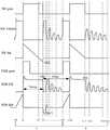
其中,波形PSR gate代表原边反馈芯片120的用于控制功率开关管Q1的导通与关断的控制信号,波形PSR Ipk代表流经原边绕组的电流(也可以称为原边电流),波形PSR FB代表用于表征输出电压的输出反馈信号,波形SR Vdrain代表副边同步整流芯片130中的同步整流开关管Q2的漏极处的电压,波形SR gate代表副边同步整流芯片130的用于控制同步整流开关管Q2的导通与关断的控制信号,波形SR Isk代表流经副边绕组的电流(也可以称为副边电流),Tdemg对应于退磁时间,Tring对应于谐振时间。各个信号的波形之间的对应关系如图5所示,为了简化描述,在此不再赘述。Among them, the waveform PSR gate represents the control signal of the
在本发明实施例提供的开关电源中,原边反馈芯片可以控制功率开关管Q1的导通和关断,副边同步整流芯片可以控制同步整流开关管Q2的导通和关断,两个开关管交互工作。In the switching power supply provided by the embodiment of the present invention, the primary-side feedback chip can control the turn-on and turn-off of the power switch Q1, the secondary-side synchronous rectifier chip can control the turn-on and turn-off of the synchronous rectifier switch Q2, and the two switches Tubes work interactively.
作为一个示例,副边同步整流芯片可以被配置为在检测到副边同步整流芯片的本体温度高于第一预设阈值时,输出温度保护请求信息,原边反馈芯片可以被配置为响应于接收到温度保护请求信息而进入自动重启状态。As an example, the secondary-side synchronous rectifier chip may be configured to output temperature protection request information when it is detected that the body temperature of the secondary-side synchronous rectifier chip is higher than the first preset threshold, and the primary-side feedback chip may be configured to respond to receiving When the temperature protection request message is received, it enters the automatic restart state.
具体地,同步整流芯片可以具有片上(On-chip)温度检测功能,当检测到同步整流开关管Q2的温度或者同步整流芯片周围的温度超过例如OTP预设值时,可以通过控制同步整流开关管Q2的延迟关断,输出温度保护请求信息,并经过变压器T1的原边主绕组或者原边辅助绕组和原边反馈芯片的CS引脚向原边反馈芯片发送温度保护请求信息,当原边反馈芯片检测到该温度保护请求信息时,可以确定同步整流开关管Q2的温度或者同步整流芯片周围的温度过高,使得原边反馈芯片进入自动重启状态,从而可以保护系统不会因为同步整流开关管Q2或者同步整流芯片的周围温度过高而出现诸如损坏同步整流开关管或者熔壳等之类的安全问题。Specifically, the synchronous rectifier chip may have an on-chip temperature detection function. When it is detected that the temperature of the synchronous rectifier switch Q2 or the temperature around the synchronous rectifier chip exceeds, for example, an OTP preset value, the synchronous rectifier switch can be controlled by controlling the temperature of the synchronous rectifier switch Q2. The delayed shutdown of Q2 outputs the temperature protection request information, and sends the temperature protection request information to the primary feedback chip through the primary side main winding or the primary side auxiliary winding of the transformer T1 and the CS pin of the primary side feedback chip. When the primary side feedback chip When the temperature protection request information is detected, it can be determined that the temperature of the synchronous rectifier switch Q2 or the temperature around the synchronous rectifier chip is too high, so that the primary side feedback chip enters an automatic restart state, so that the system can be protected from the synchronous rectifier switch Q2. Or the surrounding temperature of the synchronous rectifier chip is too high, and safety problems such as damage to the synchronous rectifier switch tube or fusion shell occur.
为了更好地理解本发明实施例提供的开关电源的工作原理,以下通过具体示例的方式对图1所示的开关电源的原边反馈芯片的具体实现方式进行介绍。参考图6,图6示出了本发明实施例提供的原边反馈芯片的结构示意图。In order to better understand the working principle of the switching power supply provided by the embodiments of the present invention, a specific implementation of the primary-side feedback chip of the switching power supply shown in FIG. 1 is described below by way of specific examples. Referring to FIG. 6 , FIG. 6 shows a schematic structural diagram of a primary-side feedback chip provided by an embodiment of the present invention.
如图6所示,该原边反馈芯片120可以包括VDD引脚、FB引脚、GND引脚、CS引脚以及Drain引脚等,并且可以包括UVLO和AVDD模块1202、参考信号生成模块1204、保护模块1206、采样模块1208、退磁检测模块1210、恒压控制模块1212、电流检测模块1214、OTP检测模块1216、恒流控制模块1218、逻辑控制模块1220以及栅极驱动模块1222等。As shown in FIG. 6 , the
作为一个示例,UVLO和AVDD模块1202的第一端连接到VDD引脚,第二端连接到参考信号生成模块1204的第一端,第三端可以输出电源良好(Power Good,PG)信号,参考信号生成模块1204的第二端可以输出参考电压Vref,保护模块1206的第一端连接到FB引脚,保护模块1206的第二端连接到逻辑控制模块1220的第一端,采样模块1208的第一端连接到FB引脚,采样模块1208的第二端连接到恒压控制模块1212的第一端,恒压控制模块1212的第二端接收Vref_cv,退磁检测模块1210的第一端连接到FB引脚,退磁检测模块1210的第二端连接到恒流控制模块1218的第一端,电流检测模块1214的第一端连接到CS引脚,电流检测模块1214的第二端连接到恒压控制模块1212的第三端,电流检测模块1214的第三端连接到恒流控制模块1218的第二端,电流检测模块1214的第四端连接到OTP检测模块1216的第一端,OTP检测模块1216的第二端连接到恒压控制模块1212的第四端,恒压控制模块1212的第五端连接到逻辑控制模块1220的第二端,恒流控制模块1218的第三端连接到逻辑控制模块1220的第三端,OTP检测模块1216的第三端和第四端分别连接到保护模块1206的第三端和逻辑控制模块1220的第四端,逻辑控制模块1220的第五端连接到栅极驱动模块1222的第一端,栅极驱动模块1222的第二端连接到功率开关管Q1的第一端和电流检测模块1214的第五端,功率开关管Q1的第二端连接到Drain引脚,功率开关管Q1的第三端连接到CS引脚。As an example, the first terminal of the UVLO and
作为一个示例,UVLO和AVDD模块1202可以被配置为向原边反馈芯片120提供工作电压和内部参考电压Vref等,其中,当VDD电压超过UVLO电压之后,PG信号可以被置为1,使得原边反馈芯片120内置的各个模块可以开始工作。As an example, the UVLO and
作为一个示例,参考信号生成模块1204可以用于向恒压控制模块1212输出参考电压Vref_cv。As an example, the reference
作为一个示例,保护模块1206主要可以由两部分保护组成,一部分可以用于基于来自FB引脚的表征输出电压的输出反馈信号进行保护,例如分压电阻开路/短路保护、辅助绕组开路保护等;并且另一部分可以用于基于来自OTP检测模块1216的OTP信号进行保护,例如,当OTP信号有效时,保护模块1206可以控制原边反馈芯片120进入自动重启状态,从而保护系统不会因为同步整流开关管的温度或者同步整流芯片周围的温度过高而出现损坏同步整流开关管或者熔壳等之类的严重问题。As an example, the
作为一个示例,退磁检测模块1210可以被配置为在功率开关管Q1处于关断状态时,基于输出反馈信号对变压器的原边绕组的退磁情况进行检测。As an example, the
具体地,退磁检测模块1210可以进一步被配置为在功率开关管Q1处于关断状态时,将输出反馈信号的上升沿上升至大于某一预设值(例如,0.1V)至输出反馈信号的下降沿下降至低于某一预设值(例如,0.1V)之间的时间段判定为原边绕组的退磁时间Tdemg(参见图5)。Specifically, the
作为一个示例,采样模块1208可以被配置为在原边绕组的退磁时间期间,对当前周期的输出反馈信号的平台电压进行采样并保持到下一个周期,并将采样电压Vs输入到恒压控制模块1212。As an example, the
作为一个示例,恒压控制模块1212可以被配置为基于采样电压Vs和表征原边电流的电压信号Vcs,生成用于控制功率开关管Q1的导通与关断的第一控制信号。As an example, the constant
具体地,恒压控制模块1212的第一端接收来自采样模块1208的采样电压Vs,第二端接收参考电压Vref_cv(其中参考电压Vref包括参考电压Vref_cv),恒压控制模块1212可以内置有控制核心运算的误差放大器EA,其中,采样电压Vs可以输入到该误差放大器EA的例如负相输入端(恒压控制模块1212的第一端),参考电压Vref_cv可以输入到误差放大器EA的例如正相输入端(恒压控制模块1212的第二端),并将两个电压进行误差放大,得到误差信号UEA,恒压控制模块1212还可以内置有脉冲宽度调制(Pulse Width Modulation,PWM)模块,用于对误差信号UEA和表征原边电流Ipk的电压信号Vcs(Vcs=Ipk*Rsense)进行脉冲宽度调制,以控制功率开关管Q1的导通时间,使得输出反馈信号VFB在输入Bulk电压和负载变化时跟随参考电压变化。Specifically, the first terminal of the constant
作为一个示例,电流检测模块1214可以被配置为对原边电流Ipk进行检测,包括正向电流检测和负向电流检测。As an example, the
具体地,当功率开关管Q1导通时,原边电流Ipk为正向电流,该电流流经输入电容Cbulk、变压器的原边绕组Npri、功率开关管Q1、电流检测电阻Rs到地,电流检测模块1214可以被配置为对正向电流的大小和宽度进行检测,并将检测结果发送到恒压控制模块1212和恒流控制模块1218。Specifically, when the power switch tube Q1 is turned on, the primary current Ipk is a forward current, and the current flows through the input capacitor Cbulk, the primary winding Npri of the transformer, the power switch tube Q1, and the current detection resistor Rs to the ground, and the current detection The
作为一个示例,恒压控制模块1212可以被配置为基于退磁情况和正向电流检测结果来控制开关电源向待充电设备提供恒定的电压,并且恒流控制模块1218可以被配置为基于退磁情况和正向电流检测结果来控制开关电源向待充电设备提供恒定的电流。As an example, the constant
此外,在原边绕组的退磁结束之后,原边电流Ipk为负向电流,该电流流经地、电流检测电阻Rs、功率开关管Q1的寄生电容、变压器的原边绕组Npri到输入电容Cbulk,电流检测模块1214可以被配置为对负向电流的大小和宽度进行检测,并将检测结果发送到OTP检测模块1216。In addition, after the demagnetization of the primary winding is completed, the primary current Ipk is a negative current, the current flows through the ground, the current detection resistor Rs, the parasitic capacitance of the power switch Q1, the primary winding Npri of the transformer to the input capacitor Cbulk, the current The
作为一个示例,OTP检测模块1216可以被配置为接收退磁情况和负向电流检测结果,根据预设规则来判断同步整流开关管Q2的温度或者同步整流芯片周围的温度是否超过预设值,并在温度超过预设值的情况下将温度保护请求信息提供给保护模块1206进行保护,原边反馈芯片120进入自动重启状态,从而保护系统不会因为同步整流开关管Q2的温度或者同步整流芯片周围的温度过高而出现损坏同步整流开关管Q2或者熔壳等之类的严重问题。As an example, the
作为一个示例,恒流控制模块1218可以被配置为基于正向电流检测信号,实现恒流模式下输出恒定电流,具体地,其可以通过外部电流检测电阻Rsense来调整恒流的大小。As an example, the constant
作为一个示例,逻辑控制模块1220可以被配置为对各个输入信号进行逻辑分析,并输出逻辑控制信号给栅极驱动模块1222,以控制功率开关管Q1的导通与关断。As an example, the
作为一个示例,栅极驱动模块1222可以被配置为在进行逻辑控制之后,使得信号实现图腾输出。As an example, the
具体地,栅极驱动模块1222可以被配置为对来自逻辑控制模块1220的信号进行处理,生成用于控制功率开关管Q1的导通与关断的控制信号。其中,功率开关管Q1的第二端可以连接到Drain引脚,第三端可以连接到CS引脚。Specifically, the
应注意,功率开关管Q1除了如图所示可以位于原边反馈芯片的内部之外,功率开关管Q1还可以独立封装,本发明对此不做限制。It should be noted that in addition to being located inside the primary feedback chip as shown in the figure, the power switch Q1 can also be packaged independently, which is not limited in the present invention.
为了更好地理解本发明实施例提供的开关电源,以下通过具体示例的方式对本发明实施例提供的开关电源中的副边同步整流芯片的具体实现方式进行详细介绍,参考图7,图7示出了本发明实施例提供的副边同步整流芯片的结构示意图。In order to better understand the switching power supply provided by the embodiment of the present invention, the specific implementation of the secondary-side synchronous rectifier chip in the switching power supply provided by the embodiment of the present invention is described in detail below by way of specific examples. Referring to FIG. 7 , FIG. 7 shows A schematic structural diagram of the secondary-side synchronous rectifier chip provided by the embodiment of the present invention is shown.
如图7所示,该副边同步整流芯片130主要可以包括Vin引脚、VDD引脚、GND引脚以及Drain引脚等,并且可以包括同步整流控制模块1302、LDO供电模块1304、参考模块1306、UVLO 1308、退磁检测模块1310、动态响应模块1312、假负载模块1314、OTP检测模块1316以及同步整流开关管Q2等。其中,同步整流控制模块1302可以包括HV开关、比较器1318、比较器1320、最小导通时间设置模块1322、RS触发器1324、逻辑控制模块1326以及栅极驱动模块1328等。As shown in FIG. 7 , the secondary-side
如图7所示,退磁检测模块1310的第一端可以连接到Drain引脚,第二端可以连接到同步整流控制模块1302的第一端,第三端可以连接到动态响应模块1312的第一端,动态响应模块1312的第二端可以连接到Vin引脚,动态响应模块1312的第三端可以连接到假负载模块1314,动态响应模块1312的第四端可以连接到同步整流控制模块1302的第二端,OTP检测模块1316可以连接到同步整流控制模块1302的第三端,同步整流控制模块1302的第四端可以连接到开关管Q2的栅极,开关管Q2的漏极可以连接到Drain引脚,源极可以接地,LDO供电模块1304的第一端可以连接到VDD引脚,LDO供电模块1304的第二端可以连接到Drain引脚,LDO供电模块1304的第三端可以连接到UVLO 1308的第一端,UVLO 1308的第二端可以输出PG信号,LDO供电模块1304的第四端可以连接到参考模块1306的第一端,参考模块1306的第二端可以输出Vref信号,LDO供电模块1304的第五端可以连接到Vin引脚和动态响应模块1312的第二端,比较器1318的第一端接收Vdrain电压(同步整流开关管Q2的漏极处的电压),第二端接地,比较器1320的第一端接收Vdrain电压,第二端接地,比较器1318的第三端经由最小导通时间控制模块1322连接到RS触发器1324的复位端,比较器1320的第三端连接到RS触发器1324的置位端,RS触发器1324的输出端可以连接到逻辑控制模块1326的第一端,逻辑控制模块1326的第二端和第三端分别可以连接到同步整流控制模块1302的第二端和第三端,逻辑控制模块1326的第四端可以连接到栅极驱动模块1328的第一端,栅极驱动模块1328的第二端可以连接到Q2的栅极。As shown in FIG. 7 , the first end of the
作为一个示例,在系统启动时,VDD电压和Vin电压都较低,同步整流开关管Q2的体二极管(body diode)导通,Vdrain用于为VDD充电使得VDD电压升高,LDO供电模块1304可以被配置为在检测到VDD电压超过UVLO电压之后,将PG(power good)信号置1,使得同步整流芯片内部的电路开始工作。As an example, when the system starts, the VDD voltage and Vin voltage are both low, the body diode of the synchronous rectifier switch Q2 is turned on, and Vdrain is used to charge VDD to increase the VDD voltage. The LDO
作为一个示例,同步整流控制模块1302可以被配置为在功率开关管Q1关断之后,副边绕组开始消磁,防止原副边共通,先是同步整流开关管Q2的体二极管导通,当VD电压小于某个电平(例如,VD<-300mV)时,控制同步整流开关管Q2的导通;随着退磁电流的逐渐减小,VD电压逐渐上升,当VD电压大于某个电平(例如,VD>-3.5mV或者0mV)时,控制同步整流开关管Q2的关断。为了防止退磁开始谐振对VD电压检测产生影响,导致同步整流开关管Q2被提前误关断,可以设置同步整流最小导通时间。As an example, the synchronous
作为一个示例,退磁检测模块1310可以被配置为对例如同步整流退磁时间、退磁频率和退磁上升沿、下降沿等进行检测,使得检测结果一方面可以用于控制同步整流开关管Q2的导通和关断,另一方面可以将检测到的退磁频率传输给动态响应模块1312。As an example, the
作为一个示例,OTP检测模块1316可以为被配置为在检测到副边同步整流芯片的本体温度高于一个预设阈值时对同步整流开关管进行延迟关断并且在本体温度低于或等于上述预设阈值时对同步整流开关管进行正常关断,向原边反馈芯片提供温度保护请求信息。As an example, the
具体地,OTP检测模块1316可以用作片上OTP保护电路,通过检测芯片的本体温度,预测同步整流芯片周围的温度或者同步整流开关管Q2的温度,并在检测到温度过高时,进行片上(On-chip)OTP保护检测,将信号传输到逻辑控制模块1326,使得逻辑控制模块1326控制栅极驱动模块1328来延迟关断同步整流开关管Q2,以将OTP保护请求信息通过变压器耦合传输到原边反馈芯片以供进行OTP保护的识别。Specifically, the
作为一个示例,动态响应模块1312可以被配置为在开关电源处于空载状态时,如果原边绕组的退磁频率小于一个预设阈值并且开关电源的输出电压大于另一预设阈值,则增加开关电源的假负载;以及在开关电源处于加载状态时,如果开关电源的输出电压小于又一预设阈值,则在经过预设时段之后向原边反馈芯片通知开关电源的负载变化,使得原边反馈芯片增大第一功率开关管的开关频率和流经原边绕组的电流。As an example, the
具体地,动态响应模块1312可以被配置为在系统输出突然空载时,这会导致输出电压升高并且工作频率降低,当检测到原边绕组的退磁频率小于某个设定阈值(例如,阈值为5kHz)并且开关电源的输出电压超过某一设定阈值(例如,阈值为5V,输出电压为5.8V)时,则增加开关电源的负载,来消耗能量;当系统瞬间加载时,这会导致输出电压瞬间降低,当检测到输出电压低于某一固定值(例如,阈值为5V,输出电压为4.6V)时,则动态响应模块1312可以在屏蔽某一固定时间(例如,100us)之后,经过变压器耦合向原边反馈芯片提供指示负载变化的信息,以告知原边反馈芯片负载的变化,提高原边功率开关管的开关频率和流经原边绕组的电流,以增大功率并提升输出电压。Specifically, the
作为一个示例,假负载模块1314可以被配置为:当系统输出瞬间空载时,由于对输出电压进行控制是通过原边辅助绕组进行检测控制的,输出电压的响应有一定延迟,空载后开关电源的输出电压冲高,为了防止输出电压上冲过高,当满足退磁频率小于某个设定阈值(例如,阈值为5kHz)并且输出电压超过某一设定阈值(例如,阈值为5V,输出电压为5.8V)时,可以增加芯片的假负载,消耗多余能量,并降低输出电压。As an example, the
应注意,同步整流开关管Q2除了如图所示可以位于副边同步整流芯片的内部之外,同步整流开关管Q2还可以独立封装,本发明对此不做限制。It should be noted that the synchronous rectification switch Q2 can be located inside the secondary side synchronous rectifier chip as shown in the figure, and the synchronous rectifier switch Q2 can also be packaged independently, which is not limited in the present invention.
可见,在图7所示的副边同步整流芯片中,当检测到同步整流开关管的温度或者同步整流芯片周围的温度超过预设OTP阈值时(例如,OTP阈值可以在芯片内部通过修调(trimming)的方式分成不同档位,其中可以根据实际设计PCB测试值来设定修调阈值),同步整流开关管Q2被延迟2us或者其他固定时间关断,通过变压器将OTP信息耦合到原边辅助绕组和原边反馈芯片的CS引脚上,原边反馈芯片可以根据预设规则对OTP信息进行检测,判断副边同步整流开关管的温度或者同步整流芯片周围的温度是否超过预设OTP阈值,并在检测到温度超过预设OTP阈值时,使得原边反馈芯片进入自动重启状态。It can be seen that in the secondary-side synchronous rectifier chip shown in FIG. 7, when the temperature of the synchronous rectifier switch tube or the temperature around the synchronous rectifier chip is detected to exceed the preset OTP threshold (for example, the OTP threshold can be adjusted inside the chip by adjusting ( The trimming) method is divided into different gears, in which the trimming threshold can be set according to the actual design PCB test value), the synchronous rectification switch Q2 is delayed by 2us or other fixed time to turn off, and the OTP information is coupled to the primary side auxiliary through the transformer On the CS pin of the winding and the primary feedback chip, the primary feedback chip can detect the OTP information according to the preset rules, and judge whether the temperature of the secondary synchronous rectification switch tube or the temperature around the synchronous rectification chip exceeds the preset OTP threshold. And when it is detected that the temperature exceeds the preset OTP threshold, the primary side feedback chip enters an automatic restart state.
为了更好地理解本发明实施例提供的温度保护检测原理,以下通过具体示例的方式对温度保护检测逻辑进行介绍。参考图8,图8示出了本发明实施例提供的温度保护周期和正常工作周期的波形示意图。In order to better understand the temperature protection detection principle provided by the embodiment of the present invention, the temperature protection detection logic is introduced below by way of a specific example. Referring to FIG. 8 , FIG. 8 shows a schematic waveform diagram of a temperature protection period and a normal working period provided by an embodiment of the present invention.
其中,波形SR gate代表副边同步整流芯片130的用于控制同步整流开关管Q2的导通与关断的控制信号,波形SR Vdrain代表副边同步整流芯片130中的同步整流开关管Q2的漏极处的电压,波形SR Isk代表副边电流,波形PSR gate代表原边反馈芯片120的用于控制功率开关管Q1的导通与关断的控制信号,波形PSR FB代表用于表征输出电压的输出反馈信号,波形PSR Ipk代表原边电流,Tdemg对应于退磁时间,Tring对应于谐振时间。The waveform SR gate represents the control signal of the secondary
如图所示,温度保护周期(对应于时间段t0至t9,标记为1)和正常工作周期(对应于时间段t9至t13,标记为0)之间的区别主要在于:在温度保护周期期间,同步整流开关管Q2被延迟某一定时间(例如,2us)关断(参考图8,在时间段t2至t3期间,SR gate波形的虚线部分),在该延迟时间段期间,副边电流Isk在下降至零之后会继续负向增大至Isk1,此时变换器的输出电压对副边绕组Nsec进行反向励磁存储能量,辅助绕组Naux上的电压继续钳位在Vaux=(V0*Naux)/Nsec,该辅助绕组Naux上的电压Vaux经过分压电阻R1、R2的分压之后,在FB引脚处维持电压平台,参考图8中的PSR FB波形。在同步整流开关管Q2被关断之后,副边处的反向励磁能量被传递至原边,例如,反向励磁能量可以通过电流检测电阻Rs、功率开关管Q1的寄生电容、原边绕组Npri和输入电容Cbulk被传递到原边,原边绕组Npri被反向退磁,导致了能量的回流,在退磁结束之后,回馈能量再次为功率开关管Q1的结电容(标记为Coss)进行充电,使得功率开关管Q1的漏源极电压被钳位在Vbulk+N*Vo。当反激式开关电源工作于准谐振(Quasi-Resonant,QR)模式,且原边电流Ipk逐步增大至0时,输出反馈信号PSR FB震荡到谷底,在轻载时可以维持原来的谐振周期继续工作,在重载时则使得原边功率开关管Q1可以被零电压导通(ZVS)。As shown, the difference between the temperature protection period (corresponding to the time period t0 to t9, labeled 1) and the normal duty cycle (corresponding to the time period t9 to t13, labeled 0) is mainly: During the temperature protection period , the synchronous rectification switch Q2 is delayed for a certain period of time (for example, 2us) to turn off (refer to FIG. 8 , during the time period t2 to t3, the dotted line part of the SR gate waveform), during the delay period, the secondary side current Isk After dropping to zero, it will continue to increase in negative direction to Isk1. At this time, the output voltage of the converter will reversely excite the secondary winding Nsec to store energy, and the voltage on the auxiliary winding Naux will continue to be clamped at Vaux=(V0*Naux) /Nsec, after the voltage Vaux on the auxiliary winding Naux is divided by the voltage dividing resistors R1 and R2, the voltage platform is maintained at the FB pin, refer to the PSR FB waveform in FIG. 8 . After the synchronous rectifier switch Q2 is turned off, the reverse excitation energy at the secondary side is transferred to the primary side. For example, the reverse excitation energy can pass through the current detection resistor Rs, the parasitic capacitance of the power switch Q1, and the primary winding Npri. and the input capacitor Cbulk are transferred to the primary side, and the primary side winding Npri is reversely demagnetized, resulting in the return of energy. After the demagnetization is completed, the feedback energy charges the junction capacitance (marked as Coss) of the power switch Q1 again, so that The drain-source voltage of the power switch Q1 is clamped at Vbulk+N*Vo. When the flyback switching power supply works in Quasi-Resonant (QR) mode, and the primary current Ipk gradually increases to 0, the output feedback signal PSR FB oscillates to the bottom of the valley, and the original resonance period can be maintained at light load Continue to work, so that the primary side power switch Q1 can be turned on by zero voltage (ZVS) under heavy load.
从图8中可以看出,在温度保护周期期间,由于同步整流开关管Q2的延迟关断,会导致温度保护周期的原边处的输出反馈信号FB的波形的下降沿的下降速率(表示为Tf1)相比于正常工作周期的输出反馈信号FB的波形的下降沿的下降速率(表示为Tf2)明显加快、温度保护周期的表征原边电流Ipk的电压信号Vcs(Vcs=Ipk*Rsense,Rsense为检测电阻,Ipk为原边电流,即,图6中的Is)的负向电压明显区别于正常工作周期的表征原边电流Ipk的电压信号Vcs的负向电压。It can be seen from Figure 8 that during the temperature protection period, due to the delayed turn-off of the synchronous rectifier switch Q2, the falling rate of the falling edge of the waveform of the output feedback signal FB at the primary side of the temperature protection period (represented as Tf1) The falling rate of the falling edge of the waveform of the output feedback signal FB (denoted as Tf2) is significantly faster than that of the normal working cycle, and the voltage signal Vcs (Vcs=Ipk*Rsense, Rsense) characterizing the primary current Ipk in the temperature protection period For the detection resistance, Ipk is the primary current, ie, Is in FIG. 6 . The negative voltage is significantly different from the negative voltage of the voltage signal Vcs representing the primary current Ipk in the normal duty cycle.
因此,可以将输出反馈信号FB的波形的下降沿和表征原边电流Ipk的电压信号Vcs的负向电压作为温度保护识别条件,形成温度保护周期1。在温度保护周期1期间,在退磁结束之后,当温度保护周期的输出反馈信号FB的波形的下降沿的下降时间Tf1小于某个阈值(例如,200ns),并且表征原边电流的原边电压Vcs的负向信号低于某个阈值(例如,-200mV)并维持一定时间(例如,150ns)时,则可以判断出具有来自副边同步整流芯片的温度保护请求信息,需要进行温度保护。也就是说,原边反馈芯片可以开始准备对后续周期进行保护识别。Therefore, the falling edge of the waveform of the output feedback signal FB and the negative voltage of the voltage signal Vcs representing the primary side current Ipk can be used as temperature protection identification conditions to form a
此外,为了避免误检测,可以将多个温度保护周期和多个正常周期的组合设置为一个温度保护编码周期。因此,可以将整个温度保护编码周期设置为多位的标志位,以为原边实施温度保护功能做好准备,例如,一个温度保护编码周期可以被设置为多个温度保护周期1和多个正常工作周期0的组合,并在编码结束后设置结束标志位。In addition, in order to avoid false detection, a combination of multiple temperature protection periods and multiple normal periods may be set as one temperature protection coding period. Therefore, the entire temperature protection coding cycle can be set as a multi-bit flag bit to prepare for the primary side to implement the temperature protection function. For example, one temperature protection coding cycle can be set as multiple
作为一个示例,可以将温度保护编码周期对应的编码设置为11010111,如图9所示,图9示出了本发明实施例提供的温度保护编码周期对应的编码。具体地,温度保护编码周期可以由8个周期组成,开始的两个周期可以为11标志位,接着的四个周期可以是0101,其代表副边同步整流芯片需要进行过温保护,请求原边反馈芯片自动重启,最后的两个周期可以是结束标志位11,在结束标志位结束之后,原边反馈芯片的OTP检测模块通过执行OTP检测功能,可以判断出副边同步整流芯片发生异常,要对副边同步整流芯片进行保护,需要使得原边反馈芯片进入自动重启状态,以防止由于副边同步整流芯片的温度过高而导致损坏同步整流开关管损坏或发生熔壳之类的问题。As an example, the code corresponding to the temperature protection coding period may be set to 11010111, as shown in FIG. 9 , which shows the code corresponding to the temperature protection coding period provided by the embodiment of the present invention. Specifically, the temperature protection coding cycle can be composed of 8 cycles, the first two cycles can be 11 flag bits, and the next four cycles can be 0101, which means that the secondary-side synchronous rectifier chip needs to perform over-temperature protection, requesting the primary side The feedback chip automatically restarts, and the last two cycles can be the end flag bit 11. After the end flag bit ends, the OTP detection module of the primary feedback chip can determine that the secondary side synchronous rectifier chip is abnormal by performing the OTP detection function. To protect the secondary-side synchronous rectifier chip, it is necessary to make the primary-side feedback chip enter an automatic restart state to prevent problems such as damage to the synchronous rectifier switch tube or the occurrence of a fusion shell due to the high temperature of the secondary-side synchronous rectifier chip.
本发明实施例提供的编码长度不限定位数,可以如上所述将编码位数设置为8位,然而,当来自副边同步整流芯片的请求信息较少时,也可以降低编码位数,当来自副边同步整流芯片的请求信息较多时,可以增加编码位数,具体的编码逻辑原理可以参见图8,简单地说,在检测到温度过高时,可以对同步整流开关管进行延迟关断,这会导致输出反馈信号的下降沿的下降速率变快和表征原边电流的电压信号Vcs降低,因此可以利用输出反馈信号的下降沿和表征原边电流的电压信号Vcs来表征编码为1。The encoding length provided by the embodiment of the present invention does not limit the number of bits, and the number of encoding bits can be set to 8 bits as described above. However, when the request information from the secondary-side synchronous rectifier chip is less, the number of encoding bits can also be reduced. When there are many request information from the secondary side synchronous rectifier chip, the number of coding bits can be increased. The specific coding logic principle can be seen in Figure 8. Simply put, when it is detected that the temperature is too high, the synchronous rectification switch can be delayed and turned off , which will lead to a faster falling rate of the falling edge of the output feedback signal and a decrease in the voltage signal Vcs representing the primary current. Therefore, the falling edge of the output feedback signal and the voltage signal Vcs representing the primary current can be used to represent the code as 1.
可见,同步整流芯片通过设置片上(on-chip)温度检测电路,可以实现对同步整流开关管的温度或者同步整流芯片周围的环境的温度检测,当检测到温度超过温度保护(Over temperature protection,简称OTP)预设值时,可以通过控制同步整流开关管Q2的延迟关断,将OTP保护请求信息传递给原边反馈芯片,原边控制系统关断,防止由于副边温度过高而出现由同步整流开关管Q2损坏引起的熔壳等之类的安全问题。It can be seen that the synchronous rectifier chip can detect the temperature of the synchronous rectifier switch tube or the environment around the synchronous rectifier chip by setting an on-chip temperature detection circuit. OTP) at the preset value, the OTP protection request information can be transmitted to the primary side feedback chip by controlling the delayed turn-off of the synchronous rectifier switch Q2, and the primary side control system is turned off to prevent the occurrence of synchronous Safety problems such as the fusion shell caused by the damage of the rectifier switch tube Q2.
综上,本发明实施例提供的隔离型开关电源、用于在原副边之间传输信息的控制电路及控制方法,可以在不增加系统元器件的基础上,实现针对同步整流芯片的温度保护功能,防止由于副边同步整流芯片的周围温度或者同步整流开关管的温度过高而导致发生损坏或者熔壳。此外,本发明实施例提供的开关电源还可以传输多种信息,以提高信息传输的多样性。In summary, the isolated switching power supply, the control circuit and the control method for transmitting information between the primary and secondary sides provided by the embodiments of the present invention can realize the temperature protection function for the synchronous rectifier chip without adding system components. , to prevent damage or shell fusion caused by the ambient temperature of the secondary-side synchronous rectifier chip or the temperature of the synchronous rectifier switch tube being too high. In addition, the switching power supply provided by the embodiments of the present invention can also transmit a variety of information, so as to improve the diversity of information transmission.
此外,本发明实施例还提供了一种用在如上的开关电源中的方法,参考图10,图10示出了本发明实施例提供的用在开关电源中的方法1000的流程示意图,可以包括如下步骤:S1010,利用副边同步整流芯片在检测到副边同步整流芯片的本体温度高于第一预设阈值时,输出温度保护请求信息;以及S1020,响应于接收到温度保护请求信息而使得原边反馈芯片进入自动重启状态。In addition, an embodiment of the present invention also provides a method for use in the above switching power supply. Referring to FIG. 10 , FIG. 10 shows a schematic flowchart of the
作为一个示例,开关电源还包括变压器,原边反馈芯片包括第一功率开关管,方法1000还可以包括利用原边反馈芯片执行以下操作:在第一功率开关管处于关断状态时,基于表征开关电源的输出电压的输出反馈信号对变压器的原边绕组的退磁情况进行检测;在检测到流经原边绕组的负向电流时,生成第一电流检测信号;基于退磁情况和第一电流检测信号,确定接收到温度保护请求信息;以及基于温度保护请求信息而进入自动重启状态。As an example, the switching power supply further includes a transformer, and the primary-side feedback chip includes a first power switch tube. The
作为一个示例,方法1000还可以包括利用原边反馈芯片执行以下操作:在检测到流经原边绕组的正向电流时,生成第二电流检测信号;以及基于退磁情况和第二电流检测信号,控制开关电源向待充电设备提供恒定的电压和电流。As an example, the
作为一个示例,方法1000还可以包括利用原边反馈芯片执行以下操作:在原边绕组的退磁时间期间,对输出反馈信号的平台电压进行采样,得到采样电压;以及基于采样电压和表征流经原边绕组的电流的电压信号,生成用于控制第一功率开关管的导通与关断的第一控制信号。As an example, the
作为一个示例,基于输出反馈信号对原边绕组的退磁情况进行检测,包括:将输出反馈信号上升至大于第二预设阈值到输出反馈信号下降至小于第二预设阈值之间的时间段作为原边绕组的退磁时间。As an example, detecting the demagnetization condition of the primary winding based on the output feedback signal includes: taking the time period between the output feedback signal rising to be greater than the second preset threshold and the output feedback signal falling less than the second preset threshold as Demagnetization time of the primary winding.
作为一个示例,基于退磁情况和第一电流检测信号,确定接收到温度保护请求信息,包括:当原边绕组的退磁结束之后,在输出反馈信号的下降沿的下降时间小于第三预设阈值并且第一电流检测信号小于第四预设阈值时,确定接收到温度保护请求信息。As an example, based on the demagnetization situation and the first current detection signal, determining that the temperature protection request information is received includes: after the demagnetization of the primary winding ends, the falling time of the falling edge of the output feedback signal is less than a third preset threshold and When the first current detection signal is less than the fourth preset threshold, it is determined that temperature protection request information is received.
作为一个示例,副边同步整流芯片包括第二功率开关管,方法1000还可以包括利用副边同步整流芯片执行以下操作:在第一功率开关管被关断之后,基于第二功率开关管的漏极电压,生成用于控制第二功率开关管的导通与关断的第二控制信号。As an example, the secondary-side synchronous rectifier chip includes a second power switch tube, and the
作为一个示例,方法1000还可以包括利用副边同步整流芯片执行以下操作:通过在检测到本体温度高于第一预设阈值时对第二功率开关管进行延迟关断并且在本体温度低于或等于第一预设阈值时对第二功率开关管进行正常关断,向原边反馈芯片提供温度保护请求信息。As an example, the
作为一个示例,基于第二功率开关管的漏极电压,生成用于控制第二功率开关管的导通与关断的第二控制信号,包括:在第二功率开关管的漏极电压小于第五预设阈值时,控制第二功率开关管处于导通状态;以及在第二功率开关管的漏极电压大于第六预设阈值时,控制第二功率开关管处于关断状态,其中,第五预设阈值小于第六预设阈值。As an example, generating the second control signal for controlling the turn-on and turn-off of the second power switch tube based on the drain voltage of the second power switch tube includes: when the drain voltage of the second power switch tube is lower than the first power switch tube When five preset thresholds are used, the second power switch is controlled to be in an on state; and when the drain voltage of the second power switch is greater than the sixth preset threshold, the second power switch is controlled to be in an off state, wherein the first The fifth preset threshold is smaller than the sixth preset threshold.
作为一个示例,方法1000还可以包括利用副边同步整流芯片执行以下操作:在原边绕组的电感和第二功率开关管的结电容发生谐振时,对第二功率开关管的最小导通时间进行设置,以防止第二功率开关管被提前误关断。As an example, the
作为一个示例,方法1000还可以包括利用副边同步整流芯片执行以下操作:在开关电源处于空载状态时,如果原边绕组的退磁频率小于第七预设阈值并且开关电源的输出电压大于第八预设阈值,则增加开关电源的假负载;以及在开关电源处于加载状态时,如果开关电源的输出电压小于第九预设阈值,则在经过预设时段之后向原边反馈芯片通知开关电源的负载变化,使得原边反馈芯片增大第一功率开关管的开关频率和流经原边绕组的电流,其中,第八预设阈值大于第九预设阈值。As an example, the
可以理解的是,以上在对开关电源进行介绍时,已经对其技术细节进行了详细描述,因此,为了简化描述,方法实施例的某些细节可以参见以上针对开关电源实施例的描述,在此不再赘述。It can be understood that, when the switching power supply is introduced above, the technical details thereof have been described in detail. Therefore, in order to simplify the description, some details of the method embodiments may refer to the above description of the switching power supply embodiments. No longer.
需要明确的是,本发明并不局限于上文所描述并在图中示出的特定配置和处理。为了简明起见,这里省略了对已知方法的详细描述。在上述实施例中,描述和示出了若干具体的步骤作为示例。但是,本发明的方法过程并不限于所描述和示出的具体步骤,本领域的技术人员可以在领会本发明的精神后,作出各种改变、修改和添加,或者改变步骤之间的顺序。It is to be understood that the present invention is not limited to the specific arrangements and processes described above and shown in the figures. For the sake of brevity, detailed descriptions of known methods are omitted here. In the above-described embodiments, several specific steps are described and shown as examples. However, the method process of the present invention is not limited to the specific steps described and shown, and those skilled in the art can make various changes, modifications and additions, or change the sequence of steps after comprehending the spirit of the present invention.
以上所述的结构框图中所示的功能块可以实现为硬件、软件、固件或者它们的组合。当以硬件方式实现时,其可以例如是电子电路、专用集成电路(ASIC)、适当的固件、插件、功能卡等等。当以软件方式实现时,本发明的元素是被用于执行所需任务的程序或者代码段。程序或者代码段可以存储在机器可读介质中,或者通过载波中携带的数据信号在传输介质或者通信链路上传送。“机器可读介质”可以包括能够存储或传输信息的任何介质。机器可读介质的示例包括电子电路、半导体存储器设备、ROM、闪存、可擦除ROM(EROM)、软盘、CD-ROM、光盘、硬盘、光纤介质、射频(RF)链路,等等。The functional blocks shown in the above-described structural block diagrams may be implemented as hardware, software, firmware, or a combination thereof. When implemented in hardware, it may be, for example, an electronic circuit, an application specific integrated circuit (ASIC), suitable firmware, a plug-in, a function card, or the like. When implemented in software, elements of the invention are programs or code segments used to perform the required tasks. The program or code segments may be stored in a machine-readable medium or transmitted over a transmission medium or communication link by a data signal carried in a carrier wave. A "machine-readable medium" may include any medium that can store or transmit information. Examples of machine-readable media include electronic circuits, semiconductor memory devices, ROM, flash memory, erasable ROM (EROM), floppy disks, CD-ROMs, optical disks, hard disks, fiber optic media, radio frequency (RF) links, and the like.
还需要说明的是,本发明中提及的示例性实施例,基于一系列的步骤或者装置描述一些方法或系统。但是,本发明不局限于上述步骤的顺序,也就是说,可以按照实施例中提及的顺序执行步骤,也可以不同于实施例中的顺序,或者若干步骤同时执行。It should also be noted that the exemplary embodiments mentioned in the present invention describe some methods or systems based on a series of steps or devices. However, the present invention is not limited to the order of the above steps, that is, the steps may be performed in the order mentioned in the embodiments, or may be different from the order in the embodiments, or several steps may be performed simultaneously.
以上所述,仅为本发明的具体实施方式,所属领域的技术人员可以清楚地了解到,为了描述的方便和简洁,上述描述的系统、模块和单元的具体工作过程,可以参考前述方法实施例中的对应过程,在此不再赘述。应理解,本发明的保护范围并不局限于此,任何熟悉本技术领域的技术人员在本发明揭露的技术范围内,可轻易想到各种等效的修改或替换,这些修改或替换都应涵盖在本发明的保护范围之内。The above are only specific implementations of the present invention. Those skilled in the art can clearly understand that, for the convenience and brevity of the description, for the specific working process of the above-described systems, modules and units, reference may be made to the foregoing method embodiments. The corresponding process in , will not be repeated here. It should be understood that the protection scope of the present invention is not limited to this. Any person skilled in the art can easily think of various equivalent modifications or replacements within the technical scope disclosed by the present invention, and these modifications or replacements should all cover within the protection scope of the present invention.
Claims (22)
Priority Applications (2)
| Application Number | Priority Date | Filing Date | Title |
|---|---|---|---|
| CN202210648568.9ACN115051573A (en) | 2022-06-09 | 2022-06-09 | Switching power supply and method for use in a switching power supply |
| TW111137372ATWI852108B (en) | 2022-06-09 | 2022-09-30 | Switching power supply and method for use in switching power supply |
Applications Claiming Priority (1)
| Application Number | Priority Date | Filing Date | Title |
|---|---|---|---|
| CN202210648568.9ACN115051573A (en) | 2022-06-09 | 2022-06-09 | Switching power supply and method for use in a switching power supply |
Publications (1)
| Publication Number | Publication Date |
|---|---|
| CN115051573Atrue CN115051573A (en) | 2022-09-13 |
Family
ID=83161341
Family Applications (1)
| Application Number | Title | Priority Date | Filing Date |
|---|---|---|---|
| CN202210648568.9APendingCN115051573A (en) | 2022-06-09 | 2022-06-09 | Switching power supply and method for use in a switching power supply |
Country Status (2)
| Country | Link |
|---|---|
| CN (1) | CN115051573A (en) |
| TW (1) | TWI852108B (en) |
Family Cites Families (5)
| Publication number | Priority date | Publication date | Assignee | Title |
|---|---|---|---|---|
| EP3282550B1 (en)* | 2016-02-05 | 2020-04-15 | Guangdong Oppo Mobile Telecommunications Corp., Ltd. | Adapter and charging control method |
| WO2019056320A1 (en)* | 2017-09-22 | 2019-03-28 | Oppo广东移动通信有限公司 | Power supply circuit, power supply device, and control method |
| EP3557747A4 (en)* | 2017-09-22 | 2020-03-18 | Guangdong Oppo Mobile Telecommunications Corp., Ltd. | Power supply circuit, power supply device, and control method |
| WO2019056303A1 (en)* | 2017-09-22 | 2019-03-28 | Oppo广东移动通信有限公司 | Power supply circuit, power supply device, and control method |
| JP7032648B2 (en)* | 2018-04-25 | 2022-03-09 | ミツミ電機株式会社 | Semiconductor devices for power supply control, switching power supply devices, and their design methods |
- 2022
- 2022-06-09CNCN202210648568.9Apatent/CN115051573A/enactivePending
- 2022-09-30TWTW111137372Apatent/TWI852108B/enactive
Also Published As
| Publication number | Publication date |
|---|---|
| TW202349819A (en) | 2023-12-16 |
| TWI852108B (en) | 2024-08-11 |
Similar Documents
| Publication | Publication Date | Title |
|---|---|---|
| US9543844B2 (en) | System and method for a switched-mode power supply | |
| CN111404403B (en) | Synchronous rectification control method and control circuit for self-adaptive detection time | |
| KR100887481B1 (en) | Resonant switching power source apparatus and method of controlling the same | |
| US9407155B2 (en) | Isolated switching converter with secondary side modulation and control method | |
| US8964430B2 (en) | Active snubber circuit and power supply circuit | |
| KR100665782B1 (en) | Switching power supply | |
| US8953341B2 (en) | Converter with reduced power consumption | |
| TWI848355B (en) | Switching power supply and method for use in switching power supply | |
| CN103887984A (en) | Isolating converter and switching power supply comprising same | |
| CN103066872A (en) | Integration switch power supply controller and switch power supply using the same | |
| Chen et al. | A novel primary-side controlled universal-input AC–DC LED driver based on a source-driving control scheme | |
| CN103490636A (en) | Quasi-resonant control method, quasi-resonant system and quasi-resonant device for switching power supplies | |
| CN103415120B (en) | Power source management driving chip and application circuit thereof | |
| CN111404391A (en) | Positive-shock active clamping driving circuit | |
| CN114726221A (en) | Zero-voltage turn-on flyback switching power supply and its control chip and control method | |
| TW201643583A (en) | Power supplies and control methods suitable for sequentially transmitting command bits from secondary side to primary side | |
| CN110635696A (en) | Power switching circuit and switching method | |
| TWI862031B (en) | Isolated switching converter and the control circuit and method thereof | |
| CN118487496A (en) | Flyback Switching Power Supply | |
| TWI842012B (en) | Switching power supply and method for use in switching power supply | |
| US12355342B2 (en) | Switch-mode converter, control method for the same, and control circuit for the same | |
| TWI649946B (en) | Power converter and method for constructing power converter | |
| CN118174559A (en) | Flyback converter circuit and electronic equipment | |
| TWI852108B (en) | Switching power supply and method for use in switching power supply | |
| TW202410621A (en) | Controller applied to a power converter and operational method thereof |
Legal Events
| Date | Code | Title | Description |
|---|---|---|---|
| PB01 | Publication | ||
| PB01 | Publication | ||
| SE01 | Entry into force of request for substantive examination | ||
| SE01 | Entry into force of request for substantive examination | ||
| CB02 | Change of applicant information | Country or region after:China Address after:201203 Shanghai Pudong New Area Zhangjiang High-tech Park, No. 168 Huatuo Road, Building 3 Commercial Center Applicant after:Angbao Integrated Circuit Co.,Ltd. Address before:201203 Shanghai Pudong New Area Zhangjiang High-tech Park, No. 168 Huatuo Road, Building 3 Commercial Center Applicant before:On-Bright Electronics (Shanghai) Co.,Ltd. Country or region before:China | |
| CB02 | Change of applicant information |