CN115039237A - Method and apparatus for increasing solar energy conversion - Google Patents
Method and apparatus for increasing solar energy conversionDownload PDFInfo
- Publication number
- CN115039237A CN115039237ACN202080085606.3ACN202080085606ACN115039237ACN 115039237 ACN115039237 ACN 115039237ACN 202080085606 ACN202080085606 ACN 202080085606ACN 115039237 ACN115039237 ACN 115039237A
- Authority
- CN
- China
- Prior art keywords
- light
- spectral
- array
- energy
- distribution
- Prior art date
- Legal status (The legal status is an assumption and is not a legal conclusion. Google has not performed a legal analysis and makes no representation as to the accuracy of the status listed.)
- Granted
Links
Images


Classifications
- H—ELECTRICITY
- H02—GENERATION; CONVERSION OR DISTRIBUTION OF ELECTRIC POWER
- H02S—GENERATION OF ELECTRIC POWER BY CONVERSION OF INFRARED RADIATION, VISIBLE LIGHT OR ULTRAVIOLET LIGHT, e.g. USING PHOTOVOLTAIC [PV] MODULES
- H02S40/00—Components or accessories in combination with PV modules, not provided for in groups H02S10/00 - H02S30/00
- H02S40/20—Optical components
- H02S40/22—Light-reflecting or light-concentrating means
- C—CHEMISTRY; METALLURGY
- C09—DYES; PAINTS; POLISHES; NATURAL RESINS; ADHESIVES; COMPOSITIONS NOT OTHERWISE PROVIDED FOR; APPLICATIONS OF MATERIALS NOT OTHERWISE PROVIDED FOR
- C09K—MATERIALS FOR MISCELLANEOUS APPLICATIONS, NOT PROVIDED FOR ELSEWHERE
- C09K11/00—Luminescent, e.g. electroluminescent, chemiluminescent materials
- C09K11/08—Luminescent, e.g. electroluminescent, chemiluminescent materials containing inorganic luminescent materials
- C09K11/77—Luminescent, e.g. electroluminescent, chemiluminescent materials containing inorganic luminescent materials containing rare earth metals
- C09K11/7766—Luminescent, e.g. electroluminescent, chemiluminescent materials containing inorganic luminescent materials containing rare earth metals containing two or more rare earth metals
- C09K11/7772—Halogenides
- G—PHYSICS
- G02—OPTICS
- G02B—OPTICAL ELEMENTS, SYSTEMS OR APPARATUS
- G02B3/00—Simple or compound lenses
- G02B3/02—Simple or compound lenses with non-spherical faces
- G02B3/08—Simple or compound lenses with non-spherical faces with discontinuous faces, e.g. Fresnel lens
- G—PHYSICS
- G02—OPTICS
- G02B—OPTICAL ELEMENTS, SYSTEMS OR APPARATUS
- G02B5/00—Optical elements other than lenses
- G02B5/20—Filters
- G02B5/22—Absorbing filters
- G02B5/223—Absorbing filters containing organic substances, e.g. dyes, inks or pigments
- H—ELECTRICITY
- H10—SEMICONDUCTOR DEVICES; ELECTRIC SOLID-STATE DEVICES NOT OTHERWISE PROVIDED FOR
- H10F—INORGANIC SEMICONDUCTOR DEVICES SENSITIVE TO INFRARED RADIATION, LIGHT, ELECTROMAGNETIC RADIATION OF SHORTER WAVELENGTH OR CORPUSCULAR RADIATION
- H10F19/00—Integrated devices, or assemblies of multiple devices, comprising at least one photovoltaic cell covered by group H10F10/00, e.g. photovoltaic modules
- H10F19/80—Encapsulations or containers for integrated devices, or assemblies of multiple devices, having photovoltaic cells
- H—ELECTRICITY
- H10—SEMICONDUCTOR DEVICES; ELECTRIC SOLID-STATE DEVICES NOT OTHERWISE PROVIDED FOR
- H10F—INORGANIC SEMICONDUCTOR DEVICES SENSITIVE TO INFRARED RADIATION, LIGHT, ELECTROMAGNETIC RADIATION OF SHORTER WAVELENGTH OR CORPUSCULAR RADIATION
- H10F77/00—Constructional details of devices covered by this subclass
- H10F77/40—Optical elements or arrangements
- H10F77/42—Optical elements or arrangements directly associated or integrated with photovoltaic cells, e.g. light-reflecting means or light-concentrating means
- H10F77/45—Wavelength conversion means, e.g. by using luminescent material, fluorescent concentrators or up-conversion arrangements
- Y—GENERAL TAGGING OF NEW TECHNOLOGICAL DEVELOPMENTS; GENERAL TAGGING OF CROSS-SECTIONAL TECHNOLOGIES SPANNING OVER SEVERAL SECTIONS OF THE IPC; TECHNICAL SUBJECTS COVERED BY FORMER USPC CROSS-REFERENCE ART COLLECTIONS [XRACs] AND DIGESTS
- Y02—TECHNOLOGIES OR APPLICATIONS FOR MITIGATION OR ADAPTATION AGAINST CLIMATE CHANGE
- Y02E—REDUCTION OF GREENHOUSE GAS [GHG] EMISSIONS, RELATED TO ENERGY GENERATION, TRANSMISSION OR DISTRIBUTION
- Y02E10/00—Energy generation through renewable energy sources
- Y02E10/50—Photovoltaic [PV] energy
- Y02E10/52—PV systems with concentrators
Landscapes
- Physics & Mathematics (AREA)
- General Physics & Mathematics (AREA)
- Optics & Photonics (AREA)
- Chemical & Material Sciences (AREA)
- Inorganic Chemistry (AREA)
- Engineering & Computer Science (AREA)
- Materials Engineering (AREA)
- Organic Chemistry (AREA)
- Photovoltaic Devices (AREA)
Abstract
Description
Translated fromChinese相关申请的交叉引用CROSS-REFERENCE TO RELATED APPLICATIONS
本申请要求于2019年10月29日以Nishikant Sonwalkar的名义临时提交的名称为“METHOD AND APPARATUS FOR INCREASED SOLAR ENERGY CONVERSION[用于增加太阳能转换的方法和设备]”的美国临时申请序列号62/927228的权益,其全部内容并入本文;并且进一步地,本申请要求于2019年10月10日以Nishikant Sonwalkar的名义临时提交的名称为“OPTICAL COATING FOR SPECTRAL CONVERSION[用于光谱转换的光学涂层]”的美国临时申请序列号62/913315的权益,其全部内容并入本文。This application claims U.S. Provisional Application Serial No. 62/927228 entitled "METHOD AND APPARATUS FOR INCREASED SOLAR ENERGY CONVERSION", provisionally filed in the name of Nishikant Sonwalkar on October 29, 2019 and further, this application claims the title "OPTICAL COATING FOR SPECTRAL CONVERSION [OPTICAL COATING FOR SPECTRAL CONVERSION] ” of U.S. Provisional Application Serial No. 62/913315, which is incorporated herein in its entirety.
技术领域technical field
本发明总体上涉及光伏材料的光谱性能,更具体地涉及具有用于入射光能的高效光谱重新映射的光学涂层的光伏设备。The present invention relates generally to the spectral properties of photovoltaic materials, and more particularly to photovoltaic devices having optical coatings for efficient spectral remapping of incident light energy.
背景技术Background technique
广泛公认的是,即使使太阳能收集更高效的增量式改进也可能具有显著的经济和环境影响。特别感兴趣的领域之一是开发用于将太阳能转换为更有效形式的改良材料。It is widely recognized that even incremental improvements to make solar energy harvesting more efficient can have significant economic and environmental impacts. One area of particular interest is the development of improved materials for converting solar energy into more efficient forms.
每种类型的光传播光学材料对光能都具有可以在波长带内变化的特征光谱响应。例如,常规光学玻璃类型在给定的范围内表现出最佳的透射率,但是在特定的波长表现出较低的透射率。各种类型的光学涂层在特定波长范围内具有可变的响应和效率。光子传感器和能量转换器(比如光伏(PV)太阳能转换器)在某些波长带比在其他波长带更高效。Each type of light propagating optical material has a characteristic spectral response to light energy that can vary within a wavelength band. For example, conventional optical glass types exhibit the best transmittance within a given range, but exhibit lower transmittance at specific wavelengths. Various types of optical coatings have variable response and efficiency within specific wavelength ranges. Photonic sensors and energy converters, such as photovoltaic (PV) solar energy converters, are more efficient in certain wavelength bands than in others.
光子转换方法已经被提出并用于补偿和调整不同类型的光学部件和材料的光谱响应。已经开发了用于上转换(UC)、下转换(DC)和其他类型的光谱响应改变的方法,所述方法用于更改特定光传播光学材料的固有响应,以希望实现可测量的和有效的性能改进。Photon conversion methods have been proposed and used to compensate and tune the spectral responses of different types of optical components and materials. Methods have been developed for up-conversion (UC), down-conversion (DC), and other types of spectral response modification for modifying the intrinsic response of a particular light-propagating optical material in the hope of achieving measurable and efficient Performance improvements.
虽然在提高PV太阳能领域的能量产生效率方面取得了一些进展,但仍存在明显的问题。在提高特别是PV应用的光谱响应以及一般的光传播材料的光谱响应方面所面临的限制中,存在与用于制造提供UC或DC功能的部件的材料相关的问题。例如,提高光伏效率的早期尝试的特征在于材料昂贵和/或对环境不利。镧系元素和稀土材料已经特别地被认为是改进光传播光学材料的光谱响应的候选物。然而,必须小心地处理这些材料以便获得证明费用、制造和潜在的废物处理困难的结果。量子点材料也面临同样的问题,并引入了许多环境安全问题,这些问题可能会阻碍它们在光伏电池中的应用。While some progress has been made in improving the efficiency of energy production in the PV solar field, significant problems remain. Among the limitations faced in improving the spectral response of PV applications in particular, and of light propagating materials in general, there are problems associated with the materials used to fabricate components that provide UC or DC functionality. For example, early attempts to improve photovoltaic efficiency were characterized by expensive materials and/or environmental concerns. Lanthanides and rare earth materials have been specifically identified as candidates for improving the spectral response of light propagating optical materials. However, these materials must be handled with care in order to achieve the results of justification costs, manufacturing and potential waste disposal difficulties. Quantum dot materials face the same problems and introduce a number of environmental safety concerns that could hinder their use in photovoltaic cells.
除了与材料相关的限制之外,还存在已经被光学材料领域的技术人员广泛接受的能量转换的已知实际原理,包括与热产生和其他实际限制相关的原理。In addition to material-related limitations, there are known practical principles of energy conversion that are widely accepted by those skilled in the art of optical materials, including principles related to heat generation and other practical limitations.
因此,可以理解,与光传播光学材料的改进的光谱性能和工程化相关的方法存在改进的空间。Thus, it can be appreciated that there is room for improvement in methods related to improved spectral performance and engineering of light propagating optical materials.
发明内容SUMMARY OF THE INVENTION
本披露内容的目的是通过提供具有改进的光谱响应和效率的材料来推进太阳能收集技术。考虑到这个目的,本披露内容提供了一种用于太阳能功率转换的设备,所述设备包括:The purpose of this disclosure is to advance solar energy harvesting technology by providing materials with improved spectral response and efficiency. With this in mind, the present disclosure provides an apparatus for solar power conversion, the apparatus comprising:
光集中器的平面阵列,光集中器以在所述阵列上复制的图案分布;a planar array of light concentrators distributed in a pattern replicated on said array;
光伏(PV)电池的平面阵列,光伏电池与光集中器对准分布;以及a planar array of photovoltaic (PV) cells distributed in alignment with light concentrators; and
光谱转换器,光谱转换器在光集中器的平面阵列与PV电池的平面阵列之间延伸,其中,光谱转换器被配置为将来自光集中器阵列的第一光谱分布的入射光转换成PV电池阵列的第二光谱分布的出射光。a spectral converter extending between the planar array of light concentrators and the planar array of PV cells, wherein the spectral converter is configured to convert incident light of the first spectral distribution from the light concentrator array into the PV cells outgoing light of the second spectral distribution of the array.
本披露内容的设备和方法提供的优点是能够配制和使用比为提高光谱效率而提出的材料对环境危害小得多的材料。The apparatus and methods of the present disclosure provide the advantage of being able to formulate and use materials that are much less harmful to the environment than those proposed for increased spectral efficiency.
对于本领域技术人员来说,所披露的发明的其他期望的目的、特征和优点可能会出现或变得明显。本发明由任何所附权利要求来限定。Other desirable objects, features and advantages of the disclosed invention may appear or become apparent to those skilled in the art. The invention is defined by any appended claims.
工业适用性Industrial Applicability
根据本披露内容的广义方面,提供了用于实现用于太阳能发电的光伏装置和相关联光传播光学材料的改进的光谱响应的设备和方法。According to broad aspects of the present disclosure, apparatus and methods are provided for achieving improved spectral response of photovoltaic devices and associated light propagating optical materials for solar power generation.
附图说明Description of drawings
图1是直观地将半导体带隙效率与电子伏特值相关联的曲线图。Figure 1 is a graph that intuitively correlates semiconductor bandgap efficiency to electron volt value.
图2是示出了太阳能的光谱分布的曲线图。FIG. 2 is a graph showing the spectral distribution of solar energy.
图3是示出了下转换的简化示意图。Figure 3 is a simplified schematic diagram showing down conversion.
图4示出了对于一定波长范围内的入射激光、多晶硅pn结产生的功率。Figure 4 shows the power generated by a polysilicon pn junction for incident laser light over a range of wavelengths.
图5是示出了实验观察的曲线图,由于相干波长处光子密度的增加,功率输出增加。Figure 5 is a graph showing experimental observations of increased power output due to increased photon density at coherent wavelengths.
图6示出了根据本披露内容的实施例的太阳能板的分解视图。6 shows an exploded view of a solar panel according to an embodiment of the present disclosure.
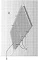
图7是组装的太阳能板的立体图。Figure 7 is a perspective view of the assembled solar panel.
图8是示出了组装的太阳能板的拐角的放大视图。FIG. 8 is an enlarged view showing a corner of the assembled solar panel.
图9是将具有和不具有光集中器和带通滤波器的能级进行比较的曲线图。Figure 9 is a graph comparing energy levels with and without optical concentrators and bandpass filters.
图10是示出具有和不具有光集中器和带通滤波器的不同布置的比较能量产生的表格。Figure 10 is a table showing comparative energy production for different arrangements with and without optical concentrators and bandpass filters.
图11是示出了为PV应用提供下转换的光处理顺序的流程图。Figure 11 is a flow diagram illustrating a light processing sequence to provide down conversion for PV applications.
图12A是示出了根据本披露内容的实施例的光传播材料的改进的光谱响应的曲线图。12A is a graph illustrating the improved spectral response of light propagating materials according to embodiments of the present disclosure.
图12B是示出了根据本披露内容的实施例的与窗格玻璃透射率相比涂布的光传播材料的改进的光谱响应的曲线图。12B is a graph showing the improved spectral response of the coated light propagating material compared to pane transmittance according to an embodiment of the present disclosure.
图12C是示出了入射光和通过传播穿过本披露内容的涂层而已经光谱偏移的光的光谱辐照度的曲线图。12C is a graph showing the spectral irradiance of incident light and light that has been spectrally shifted by propagating through the coatings of the present disclosure.
图12D是示出了使用不同涂层进行光谱转换时光谱辐照度相对于eV能量的曲线图。Figure 12D is a graph showing spectral irradiance versus eV energy for spectral conversion using different coatings.
图12E是示出了以每单位面积每秒的光子数测量的相对光通量变化的对应曲线图。Figure 12E is a corresponding graph showing relative luminous flux change measured in photons per second per unit area.
图13是示出了用于光能下转换的多层涂层的示意性侧视图。Figure 13 is a schematic side view showing a multilayer coating for down-conversion of light energy.
图14是示出了在下转换涂层中使用的布拉格反射的分层布置的侧视示意图。Figure 14 is a schematic side view showing a layered arrangement of Bragg reflections used in a down conversion coating.
图15是示出了根据本披露内容的实施例形成的用于透明下转换(DC)膜或涂层的分层布置的截面局部分解视图。15 is a cross-sectional partially exploded view illustrating a layered arrangement for a transparent down-conversion (DC) film or coating formed in accordance with an embodiment of the present disclosure.
图16示出了在涂层内增材制造和形成原位纳米粒子的顺序。Figure 16 shows the sequence of additive manufacturing and formation of in situ nanoparticles within a coating.
图17是示出了根据本披露内容的实施例的用于光谱转换的各种涂层的示例性数据的图表。17 is a graph showing exemplary data for various coatings for spectral conversion in accordance with embodiments of the present disclosure.
具体实施方式Detailed ways
本文示出和描述的附图展示了根据各种实施例的光学设备的操作和制造的关键原理,并且不是为了示出实际尺寸或比例而绘制的。为了强调基本的结构关系或操作原理,一些视觉夸张可能是必要的。The drawings shown and described herein illustrate key principles of operation and manufacture of optical devices according to various embodiments, and are not drawn to illustrate actual size or scale. Some visual exaggeration may be necessary to emphasize basic structural relationships or principles of operation.
在本披露内容的上下文中,术语“顶部”和“底部”或“上方”和“下方”是相对的,并不指示部件或表面的任何必要的取向,而是简单地用于指代和区分部件或材料块内的相反表面或不同光路。类似地,术语“水平”和“竖直”可以相对于附图使用,以描述例如不同平面中的部件或光的相对正交关系,但是不指示部件相对于真实水平和竖直取向的任何所需取向。In the context of this disclosure, the terms "top" and "bottom" or "above" and "below" are relative and do not denote any necessary orientation of components or surfaces, but are simply used to refer to and distinguish Opposite surfaces or different light paths within a part or block of material. Similarly, the terms "horizontal" and "vertical" may be used with respect to the drawings to describe, for example, the relative orthogonality of components or lights in different planes, but not to indicate any all orientation of components relative to true horizontal and vertical. orientation required.
当使用它们时,术语“第一”、“第二”、“第三”等不一定表示任何顺序或优先关系,而是用于将一个要素或时间间隔与另一个要素或时间间隔更清楚地区分开来。例如,在本文教导的内容中没有固定的“第一”或“第二”要素;在本披露内容的上下文中,这些描述符仅仅用于将一个要素和另一个类似的要素清楚地区分开来。When used, the terms "first," "second," "third," etc. do not necessarily denote any order or priority relationship, but rather are used to more clearly distinguish one element or time interval from another element or time interval separate. For example, there is no fixed "first" or "second" element in the teachings herein; in the context of the present disclosure, these descriptors are only used to clearly distinguish one element from another, similar element.
在本披露内容的上下文中,术语“膜”可以用来表示作为一个或多个薄层施加到基材上的涂层,比如由相继形成的材料层形成的薄膜光学涂层,所述材料层被处理成具有不同的折射率。膜也可以是由一层或多层光学材料形成的光传播基材,所述光传播基材以独立的方式使用,或者比如使用粘合剂光学地联接到另一个光学部件。In the context of this disclosure, the term "film" may be used to denote a coating applied to a substrate as one or more thin layers, such as a thin-film optical coating formed from successively formed layers of material that are are processed to have different indices of refraction. The film may also be a light-transmitting substrate formed from one or more layers of optical material, used in a stand-alone fashion, or optically coupled to another optical component, such as using an adhesive.
如本文所使用的,术语“可激励的”涉及在接收到功率时以及可选地在接收到使能信号时执行指示的功能的装置或一组部件。“光传播”材料传输或传送材料接收的大部分光(至少超过50%)。用于PV转换的光传播的感兴趣的范围通常在大约200nm至2200nm之间。As used herein, the term "activatable" refers to a device or group of components that performs an indicated function when power is received and optionally an enable signal is received. A "light propagating" material transmits or transmits the majority of the light (at least over 50%) that the material receives. The range of interest for light propagation for PV conversion is typically between about 200 nm to 2200 nm.
术语“纳米粒子”通常指具有介于单个原子与宏观大块固体之间的中间尺寸的粒子,其平均直径在约1nm到100nm之间。材料的纳米粒子尺寸通常近似于材料的玻尔激子半径(Bohr exciton radius)或德布罗意波长(Broglie wavelength),这可以允许单个纳米粒子在粒子内捕获单个或离散数量的电荷载流子(电子或空穴)或激子。纳米粒子对电子(或空穴)的空间限制被认为改变了材料的物理特性、光学特性、电子特性、催化特性、光电特性和磁性。The term "nanoparticles" generally refers to particles having sizes intermediate between a single atom and a macroscopic bulk solid, with an average diameter between about 1 nm and 100 nm. The nanoparticle size of a material is often approximated by the material's Bohr exciton radius or de Broglie wavelength, which can allow a single nanoparticle to trap single or discrete numbers of charge carriers within the particle (electrons or holes) or excitons. The spatial confinement of electrons (or holes) by nanoparticles is thought to alter the physical, optical, electronic, catalytic, optoelectronic and magnetic properties of the material.
PV装置或系统的能量输出与适当能带的可见光子吸收水平成比例。提高对产生能量的波长的吸收可以显著提高太阳能发电的效率,从而降低能源成本,现在使用早期PV设备的改造和重建的相关优势。The energy output of a PV device or system is proportional to the visible photon absorption level of the appropriate energy band. Improving the absorption of the wavelengths that produce energy can significantly increase the efficiency of solar power generation, thereby reducing energy costs, now using the associated advantages of retrofit and rebuilding of earlier PV equipment.
太阳能电池的功能和效率Solar Cell Function and Efficiency
为了更好地理解本披露内容提供的解决方案的性质和范围,回顾PV装置中典型太阳能电池的基本操作是有益的。典型的太阳能电池是具有耗尽区域的硅pn结二极管。在没有光的情况下,电池的行为类似于二极管。当光入射到电池上时,光子被硅吸收。这种增加的能量激发了硅电子,引起从价带到导带的跃迁,其中,电子自由移动。这些被激发的电子被称为“自由载流子”。电子跃迁产生了对应的空位,称为“空穴”。由于在耗尽区域复合形成中性原子,在耗尽区域上产生电势。连接到p区域和n区域的金属触点为这些电子提供了流动路径,即,外部电路。电子可以根据这个电势移动并与空穴复合。电子的这种运动产生电流,因此硅电池就像蓄电池一样。To better understand the nature and scope of the solutions provided by this disclosure, it is instructive to review the basic operation of a typical solar cell in a PV device. A typical solar cell is a silicon pn junction diode with a depletion region. In the absence of light, the battery behaves like a diode. When light hits the cell, the photons are absorbed by the silicon. This increased energy excites silicon electrons, causing transitions from the valence band to the conduction band, where the electrons move freely. These excited electrons are called "free carriers". The electron transitions create corresponding vacancies, called "holes". Due to the recombination of neutral atoms in the depleted region, an electric potential is generated across the depleted region. Metal contacts connected to the p- and n-regions provide a flow path for these electrons, ie, an external circuit. Electrons can move according to this potential and recombine with holes. This movement of electrons generates electrical current, so silicon cells act like accumulators.
现有PV电池的固有限制包括热力学限制,包括肖克利-奎伊瑟(S-Q)极限。从热力学角度来看,可以假设太阳和太阳能电池都是“黑体”,全部太阳能成法线角度入射到电池表面上。假设卡诺功(Carnot work)是由热力发动机从电池中取得的。对于5760k的太阳温度和300k的环境温度,在2470k的电池下可以获得最大85%的效率。在此极限处,认为所有的光子将被吸收;不存在热耗散,并且从每个光子提取最大的功。The inherent limitations of existing PV cells include thermodynamic limitations, including the Shockley-Quiser (S-Q) limit. From a thermodynamic point of view, it can be assumed that both the sun and the solar cell are "black bodies", with all solar energy incident on the cell surface at a normal angle. It is assumed that Carnot work is obtained from the battery by the heat engine. For a solar temperature of 5760k and an ambient temperature of 300k, a maximum efficiency of 85% can be obtained at a cell of 2470k. At this limit, it is believed that all photons will be absorbed; there is no heat dissipation, and maximum work is extracted from each photon.
S-Q极限将半导体电池建模为具有单个pn结的一种材料。假设能量高于带隙的所有入射光子每个光子产生一个电子空穴对。光子的所有多余的能量都转换成热能。S-Q极限基于一个太阳的非集中太阳辐射入射到PV电池上的假设。入射光子通量密度非常低,并且可以使用廉价的光学器件增加最高到大约500倍。The S-Q limit models semiconductor cells as one material with a single pn junction. It is assumed that all incident photons with energies above the band gap generate one electron-hole pair per photon. All the excess energy of the photon is converted into heat energy. The S-Q limit is based on the assumption that a sun's unconcentrated solar radiation is incident on the PV cell. Incident photon flux density is very low and can be increased up to about 500 times using inexpensive optics.
为了使半导体电子移动到外部负载电路中,其能级必须从其正常价能级增加到其更高的能量传导能级。提升到更高的能级所需的能量的量被称为“带隙”能量。能量高于带隙能量的所有光子都可以产生载流子电子,从而产生电流。然而,仅等于带隙能量的能量被用来激发电子,剩余的多于能量被转换为热能。电池的发热增加了暗电流并降低了电池的总输出。因此,如果光子接近光伏太阳能电池的pn结的带隙,则大部分光子被吸收,而其余光子会被反射,因为这些光子对产生电子空穴对没有贡献,而是对太阳能电池进行加热,引起暗电流增加。In order for a semiconductor electron to move into an external load circuit, its energy level must be increased from its normal valence energy level to its higher energy conduction energy level. The amount of energy required to lift to a higher energy level is called the "bandgap" energy. All photons with energies above the bandgap energy can generate carrier electrons and thus currents. However, only energy equal to the bandgap energy is used to excite electrons, and the remaining excess energy is converted into heat energy. Heating of the battery increases dark current and reduces the overall output of the battery. Therefore, if the photons are close to the bandgap of the pn junction of the photovoltaic solar cell, most of the photons are absorbed and the rest are reflected because these photons do not contribute to the generation of electron hole pairs, but heat the solar cell, causing Dark current increases.
聚光光伏器件(CPV)面临pn结温度升高使效率下降的问题,导致暗电流升高,引起电子和空穴复合并且减少导带中的电荷。Concentrator photovoltaics (CPVs) face the problem of decreased efficiency with increased pn junction temperature, resulting in increased dark current, recombination of electrons and holes, and reduced charge in the conduction band.
在所提出的光子太阳能转换的实施例中,使用光学涂层仅允许接近被照射的pn结的带隙能量的光子到达太阳能电池。一旦使用光学涂层消除了在pn结的带隙处未被吸收的光子(即,否则会导致太阳能电池发热的光子),集中的太阳辐射就可以线性地增加发电量,光子密度也对应增加。In the proposed embodiment of photonic solar energy conversion, the use of an optical coating allows only photons close to the bandgap energy of the illuminated pn junction to reach the solar cell. Once the unabsorbed photons at the bandgap of the pn junction (i.e., photons that would otherwise cause the solar cell to heat up) are eliminated using the optical coating, concentrated solar radiation can linearly increase power generation, with a corresponding increase in photon density.
例如,在以下披露内容中描述了使用光学涂层来提高PV电池的能量输出:For example, the use of optical coatings to improve the energy output of PV cells is described in the following disclosure:
Gadomsky的美国专利申请公开号2008/0171191 A1描述了一种纳米结构的抗反射光学涂层的用途。然而,光子太阳能转换的现有实施例仅使用纳米光学涂层作为带通滤波器。US Patent Application Publication No. 2008/0171191 Al to Gadomsky describes the use of a nanostructured antireflective optical coating. However, existing embodiments of photonic solar energy conversion only use nano-optical coatings as bandpass filters.
Kost的美国专利申请公开号2009/0084963 A1描述了用于增强光子下转换的设备和方法,所述设备和方法利用具有许多层来捕获光子,但是没有使用纳米光学涂层或光集中器。US Patent Application Publication No. 2009/0084963 A1 to Kost describes an apparatus and method for enhancing photon downconversion utilizing having many layers to capture photons, but without the use of nano-optical coatings or light concentrators.
Songo Jin等人的专利申请公开号WO 2015/138990 A1描述了太阳能吸收涂层和涂层的制造方法,所述涂层吸收一个波长区域内的太阳光谱并反射光谱的另一部分上的太阳能。然而,功率输出却令人失望。Patent Application Publication No. WO 2015/138990 A1 to Songo Jin et al. describes solar energy absorbing coatings that absorb solar spectrum in one wavelength region and reflect solar energy in another part of the spectrum and methods of making coatings. However, the power output is disappointing.
Cho等人的美国专利申请公开号2006/0169971 A1描述了一种能量转换膜和量子点膜,量子点膜使用各种量子点尺寸来增强太阳能转换,从而有助于将高能量太阳辐射转换成低能量太阳辐射。US Patent Application Publication No. 2006/0169971 A1 to Cho et al. describes an energy conversion film and a quantum dot film that uses various quantum dot sizes to enhance solar energy conversion, thereby helping to convert high-energy solar radiation into Low energy solar radiation.
已经提出了在光伏电池中更高度集中的太阳辐射的各种光学几何形状,但是未能维持更高的效率。在很大程度上,这种缺点是由于太阳能电池在集中的太阳辐射下温度升高。在本披露内容的实施例中,由于光学涂层仅允许能量接近带隙的光子入射到太阳能电池上,消除了引起发热的大部分较高能量的光子,因此太阳能电池的发热被大大减少或消除。Various optical geometries for more highly concentrated solar radiation in photovoltaic cells have been proposed, but higher efficiencies have not been maintained. To a large extent, this disadvantage is due to the increased temperature of solar cells under concentrated solar radiation. In embodiments of the present disclosure, heating of the solar cell is greatly reduced or eliminated because the optical coating allows only photons with energies close to the bandgap to impinge on the solar cell, eliminating most of the higher energy photons that cause heating .
迄今为止,重要的行业研究集中于提高硅基太阳能电池的效率,同时提高效率并降低成本。然而,很少有人注意到落在作为发电基础的PN结上的太阳光谱的调节。在提出的创新中,重点是达到太阳能电池带隙的光子,以实现最大吸收。通过正确选择和分布光能,光子可以被调节为匹配光伏太阳能电池的带隙。这种方法证明比制造多结太阳能电池(例如,串叠型太阳能电池)更有前景,制造多结太阳能电池是一种由于昂贵的带隙工程化而可能变得成本过高的方法。To date, significant industry research has focused on improving the efficiency of silicon-based solar cells while increasing efficiency and reducing costs. However, little attention has been paid to the modulation of the solar spectrum falling on the PN junction that is the basis for power generation. In the proposed innovation, the focus is on photons reaching the bandgap of the solar cell for maximum absorption. With the correct selection and distribution of light energy, photons can be tuned to match the bandgap of photovoltaic solar cells. This approach proves to be more promising than fabricating multijunction solar cells (eg, tandem solar cells), a method that can become cost prohibitive due to expensive bandgap engineering.
图1示出了黑体条件下效率限制与半导体带隙的关系,针对多种类型的太阳能电池材料,对于每个光子一个电子空穴对设置了S-Q(Shockley-Queisser)极限。过多的光子会因热和其他效应而损失。已经发现,约47%的入射能量作为热量损失掉了;18%的能量没有被转换并穿过太阳能电池;在复合效应中损失了2%的能量。最多剩下的33%的能量可以转换为电能。因此,硅太阳能电池的理论S-Q极限是33%。在以上效率计算中没有考虑由于光学布置和制造缺陷造成的损失。Figure 1 shows the relationship between the efficiency limit and the semiconductor band gap under blackbody conditions, with the S-Q (Shockley-Queisser) limit set for one electron-hole pair per photon for various types of solar cell materials. Too many photons are lost to heat and other effects. It has been found that about 47% of the incident energy is lost as heat; 18% of the energy is not converted and passed through the solar cell; and 2% of the energy is lost in the recombination effect. Up to the remaining 33% of the energy can be converted into electricity. Therefore, the theoretical S-Q limit for silicon solar cells is 33%. Losses due to optical arrangement and manufacturing defects are not considered in the above efficiency calculations.
尽管使用镧系元素和量子点已经显示了某种成功,但是,这些材料仍然相当昂贵,并且在没有重大环境问题的情况下对于广泛的商业应用来说是不可接受的。响应于对改进材料和结果的需求,申请人已经发现,结合适当构造并嵌入金属氧化物中的纳米粒子的特定布置可以实现700nm到1100nm的带通以及300nm到600nm波长的太阳光子向800nm到900nm低能光子的低百分比下移。实验涂层的透射和反射光谱已经通过独立测试得到验证。室外测试表明72电池全尺寸板的效率增益,基于室外现场试验,太阳能板效率的总体提高平均为15%至22%。Although the use of lanthanides and quantum dots has shown some success, these materials are still quite expensive and unacceptable for broad commercial applications without significant environmental concerns. In response to the need for improved materials and results, Applicants have discovered that a bandpass of 700nm to 1100nm and 300nm to 600nm wavelengths of solar photons to 800nm to 900nm can be achieved in combination with a specific arrangement of nanoparticles that are appropriately structured and embedded in metal oxides. Low percentage of low energy photons shift down. The transmission and reflection spectra of the experimental coatings have been verified by independent testing. Outdoor testing demonstrated efficiency gains for the 72-cell full-scale panels, with an overall increase in solar panel efficiency averaging 15% to 22% based on outdoor field tests.
根据本披露内容的实施例,如随后更详细描述的,使用工程化纳米光学涂层的光子太阳能转换(PSC)工艺可以将具有包括紫外(UV)波长和一部分可见光的波长的高能光子下转换为更接近地调谐到c-Si电池的带隙的低能光。这种类型的将光能调节到更适合能量转换的水平的下转换能够增加光子电池的外部量子效率(EQE)。根据申请人的过程使用下转换形成的涂层可以将常规的低成本太阳能板的效率提高15%到22%。在更广泛的方面,本披露内容的实施例可以用于提供入射光的波长偏移,包括例如下转换、上转换和带隙变窄。According to embodiments of the present disclosure, as described in more detail subsequently, a photonic solar energy conversion (PSC) process using engineered nano-optical coatings can down-convert high-energy photons having wavelengths including ultraviolet (UV) wavelengths and a portion of visible light into Low-energy light tuned more closely to the bandgap of c-Si cells. This type of downconversion, which modulates light energy to a level more suitable for energy conversion, can increase the external quantum efficiency (EQE) of the photonic cell. The use of down-conversion-formed coatings according to Applicants' process can increase the efficiency of conventional low-cost solar panels by 15% to 22%. In broader aspects, embodiments of the present disclosure may be used to provide wavelength shifting of incident light, including, for example, down-conversion, up-conversion, and bandgap narrowing.
如图2中的太阳辐射光谱曲线图所示,太阳能的波长范围为约300nm到2400nm。使用1064nm的带隙,对于太阳能PV转换最有效的波长在约400nm到1200nm之间的范围内。As shown in the solar radiation spectrum graph in Figure 2, the wavelength of solar energy ranges from about 300 nm to 2400 nm. Using a band gap of 1064 nm, the most efficient wavelengths for solar PV conversion are in the range between about 400 nm to 1200 nm.
图3以简化示意图形式示出了光谱下转换的机制,其中,一个高能光子被转换成两个低能光子。在光传播材料中提供这种类型的光谱转换的常规解决方案严重依赖镧系元素材料。Figure 3 shows the mechanism of spectral down-conversion in simplified schematic form, where one high-energy photon is converted into two low-energy photons. Conventional solutions to provide this type of spectral conversion in light propagating materials rely heavily on lanthanide materials.
作为一种常规做法,已知使用具有量子点和镧系元素离子的光致发光下转换层(PDL)来管理太阳光谱以调节光并执行下转换措施。原则上,如图3的简化图示意性地所示,由于一个高能光子的共振转移产生两个或更多个低能光子而发生下转换,引起外部量子效率(EQE)的增益超过100%。As a common practice, it is known to use photoluminescent downconversion layers (PDLs) with quantum dots and lanthanide ions to manage the solar spectrum to modulate light and perform downconversion measures. In principle, downconversion occurs due to the resonant transfer of one high-energy photon generating two or more low-energy photons, as schematically shown in the simplified diagram of Fig. 3, resulting in a gain of more than 100% in external quantum efficiency (EQE).
例如,在氟化钇YF3主体中具有镨Pr3+的镧系离子层中,185nm波长的具有高能量的光子(大约6700meV)首先被镧系元素离子吸收,然后下转换成408nm和620nm(大约3040-2000meV)的两个低能光子。所述过程分两步完成;首先:For example, in a lanthanide ion layer with praseodymium Pr3+ in the yttrium fluoride YF3 host, a photon with high energy at 185 nm wavelength (about 6700 meV) is first absorbed by the lanthanide ion and then down-converted to 408 nm and 620 nm (about 3040- 2000meV) of two low-energy photons. The process is accomplished in two steps; first:
1S0→3P1,波长408nm;1 S0 →3 P1 , wavelength 408 nm;
然后,第二次转换3P1→3F2,波长620nm。Then, the second conversion is3 P1 →3 F2 at a wavelength of 620 nm.
将高能光子下移到大量低能光子的过程增大了一个光子产生多于一个电子的可能性,从而提高了外部量子效率。The process of moving high-energy photons down to a large number of lower-energy photons increases the likelihood that one photon will produce more than one electron, thereby increasing the external quantum efficiency.
用于能量下转换的常规方法中的镧系元素的用途和优点是很好理解的。作为镧系元素特征的各种状态的电子的可用性使得这些物质容易用于下转换应用。同时,其他元素没有这种固有的优势,并且不会被认为是制造下转换制品的可能候选材料。The use and advantages of lanthanides in conventional methods of energy downconversion are well understood. The availability of electrons in various states that are characteristic of lanthanides makes these materials readily available for downconversion applications. At the same time, other elements do not have this inherent advantage and would not be considered as possible candidates for the manufacture of down-conversion articles.
然而,镧系元素材料在成本、可获得性、处理方面存在许多问题,并且引入了许多环境问题。镧系元素也表现出相当大的损失,这限制了可以获得多少改进。However, lanthanide materials present many problems with cost, availability, handling, and introduce many environmental concerns. Lanthanides also show considerable losses, which limits how much improvement can be achieved.
光子太阳能转换Photonic solar energy conversion
申请人的用于提高光伏效率和用于光谱调节具有价值的其他应用的方法不取决于镧系元素或基于磷光体的光产生来使光的波长偏移以提高太阳能转换的效率。相反,申请人已经确定了用于光处理和能量转换的新型顺序、以及对应的分层结构,所述分层结构可以被工程化成提供对于光伏应用和其他应用最有效的下转换。申请人的技术将量子匹配应用于波长偏移问题,形成了利用布拉格反射特性和表面增强拉曼散射效率的多层结构。Applicants' approach for improving photovoltaic efficiency and for other applications where spectral tuning is valuable does not depend on lanthanide or phosphor-based light generation to shift the wavelength of light to increase the efficiency of solar energy conversion. Instead, Applicants have identified novel sequences for light processing and energy conversion, and corresponding layered structures that can be engineered to provide the most efficient downconversion for photovoltaic and other applications. Applicants' technique applies quantum matching to the wavelength shifting problem, resulting in multilayer structures that exploit Bragg reflection properties and surface-enhanced Raman scattering efficiency.
值得注意的是,本披露内容的实施例可以用于提高已经安装的太阳能板的性能。申请人结合了多项创新,以便提高现有太阳能板的功率输出,包括以下内容:Notably, embodiments of the present disclosure may be used to enhance the performance of already installed solar panels. Applicants have combined several innovations in order to increase the power output of existing solar panels, including the following:
(i)光子光谱调节。将太阳辐射转换为波长接近PV电池的带隙能量的相干光能。(i) Photonic spectral tuning. Converts solar radiation to coherent light energy with wavelengths close to the bandgap energy of the PV cell.
(ii)充当带通滤波器和光谱转换器的纳米光学涂层,所述纳米光学涂层传输能级(波长)接近PV电池带隙能量的光子。根据实施例,通过应用一组金属氧化物涂层而产生的光谱转换器用于将来自入射太阳光的辐射转换成接近800nm峰值的最佳波长附近的100nm的带通。一旦滤光器/光谱转换器层被施加在光伏板上,光集中器被用于将太阳辐射的强度增加到每单位面积5倍到15倍太阳,从而增加具有接近最佳波长的入射光子的密度。(ii) Nano-optical coatings acting as bandpass filters and spectral converters that transmit photons with energy levels (wavelengths) close to the PV cell bandgap energy. According to an embodiment, a spectral converter produced by applying a set of metal oxide coatings is used to convert radiation from incident sunlight into a bandpass of 100 nm near the optimum wavelength near the 800 nm peak. Once the filter/spectral converter layer is applied on the photovoltaic panel, light concentrators are used to increase the intensity of solar radiation by a factor of 5 to 15 times the sun per unit area, thereby increasing the incidence of incident photons with near-optimal wavelengths density.
(iii)使用至少一种聚光方法(比如聚焦在PV电池上的光集中器)增加光子密度。根据实施例,涂有用于最佳波长的带通滤波器的菲涅耳透镜的蜂窝被设计成实现太阳能电池的功率输出增加5倍。(iii) Increase the photon density using at least one light concentrating method, such as a light concentrator focused on the PV cell. According to an embodiment, a honeycomb coated with a Fresnel lens of a bandpass filter for optimal wavelengths is designed to achieve a 5-fold increase in the power output of the solar cell.
用于优化性能的目标波长可以通过测量具有可变波长固态激光器的给定半导体太阳能电池的频率响应来确定。激光输出可以在一定范围内变化(比如从600nm增加到1100nm),同时在所述范围内的增量点处测量输出和效率。可以相应地绘制响应曲线。The target wavelength for optimizing performance can be determined by measuring the frequency response of a given semiconductor solar cell with a variable wavelength solid state laser. The laser output can be varied over a range (such as increasing from 600 nm to 1100 nm), with output and efficiency being measured at incremental points within the range. Response curves can be drawn accordingly.
举例来说,图4的曲线图示出了对于一定波长范围内的入射激光由多晶硅pn结产生的功率。最佳值400在800nm附近的峰值输出处。For example, the graph of Figure 4 shows the power generated by a polysilicon pn junction for incident laser light over a range of wavelengths. The optimum value of 400 is at the peak output around 800nm.
图5的曲线图示出了实验观察,由于相干波长处光子密度的增加,电流输出增加。如图5所示,入射到太阳能电池上的最佳波长激光束的相干光子强度的增加线性地增加了发电量。The graph of Figure 5 shows the experimental observation that the current output increases due to the increase in photon density at the coherent wavelength. As shown in Figure 5, the increase in the coherent photon intensity of the optimal wavelength laser beam incident on the solar cell linearly increases the power generation.
为pn结引导最佳波长的光而提供的滤光器用于阻挡对在PV板中产生电能无用的所有其他光子。The filters provided for the pn junction to direct the best wavelengths of light are used to block all other photons that are not useful for generating electrical energy in the PV panel.
如图5所示,x轴表示固态激光器的功率输入,具有期望波长的光子照射目标pn结作为Pin功率输入。y轴表示最大功率输出Pmax。功率输出随着功率输入的增加而线性地增加。这表明接近太阳能电池的带隙能量(匹配能量)的光子对应地提高了光子转换成电的效率。在发电量随着光子强度的增加而线性地增加的情况下,光子转换到合适的功率水平。As shown in Figure 5, the x-axis represents the power input of the solid-state laser, and photons with the desired wavelength irradiate the target pn junction as the Pin power input. The y-axis represents the maximum power output Pmax. Power output increases linearly with power input. This indicates that photons close to the bandgap energy (matching energy) of the solar cell correspondingly increase the efficiency of photon conversion into electricity. With the power generation increasing linearly with the intensity of the photons, the photons are converted to a suitable power level.
本披露内容的实施例使用PV板基材上的光集中器和光谱转换光学涂层的组合来增加发电量。Embodiments of the present disclosure use a combination of light concentrators and spectral conversion optical coatings on PV panel substrates to increase power generation.
太阳能板布置Solar panel arrangement
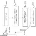
图6示出了根据本披露内容的实施例形成的太阳能板600的分解视图。光集中器层620具有透镜元件阵列622,比如相邻菲涅耳透镜阵列,用于集中光并将集中的光沿着光路导向排列在PV阵列610上的PV电池612。带通滤波器/光谱调节器630设置在光路中的适当位置,用于调节在光集中器与PV阵列之间传送的光;光谱调节器630可以形成在具有光学涂层的玻璃层或其他光学透明材料层上或其内。根据替代实施例,光集中器阵列620和光谱调节器630的相对位置可以与图6中所示的相反,使得在光路上,入射太阳光的滤波和光谱转换先于光集中。FIG. 6 shows an exploded view of a
图7示出了太阳能板600,所述太阳能板是根据实施例使用各种类型的夹具、支架或其他紧固件640将阵列610、滤波器/光谱调节器630和集中器620一起保持在适当位置作为单个单元组装的。根据本披露内容的实施例,与分层部件的面对表面相对应的相邻平行平面之间的距离小于20mm。例如,此距离可以变化以适应光集中器的特定布置,或者用于改进PV或光调节部件的性能。FIG. 7 illustrates a
根据本披露内容的实施例,部件610、620和630之间的间距可以是可调节的。According to embodiments of the present disclosure, the spacing between
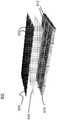
图8是示出了组装后的太阳能板600的拐角部分的特写视图。FIG. 8 is a close-up view showing a corner portion of the assembled
改造应用Retrofit applications
为了对具有PV装置阵列的现有太阳能板进行改造,本披露内容的实施例提供了光集中器620和带通滤波器/光谱调节器630的合适层。使用模块化方法,光集中器层620和带通滤波器/光谱调节器630可以被设计、缩放和框定,以适应太阳能板的尺寸和阵列几何形状。To retrofit existing solar panels with PV device arrays, embodiments of the present disclosure provide suitable layers of
光集中器620
为了增加穿过纳米光学涂层或使能的光子带通滤波器层的光子的数量,光集中器的主层(比如菲涅耳透镜集中器阵列(具有蜂窝式布置))可以层叠在光子带通滤波器上。使用低聚光光学器件(3X-5X)与带通滤波器和相干性增强纳米涂层的组合的装置可以显著增加常规光伏板的能量产生。To increase the number of photons passing through the nano-optical coating or enabled photonic bandpass filter layer, a main layer of light concentrators (such as an array of Fresnel lens concentrators (with a honeycomb arrangement)) can be stacked on the photonic band on the pass filter. Devices using low concentration optics (3X-5X) in combination with bandpass filters and coherence-enhancing nanocoatings can significantly increase the energy production of conventional photovoltaic panels.
光集中器的平面阵列对于紧凑封装来说是最有利的。除了菲涅耳透镜元件之外,还可以使用各种类型的光集中器。例如,平面光集中器可以包括例如全息透镜阵列和GRIN(梯度折射率)透镜阵列。Flat arrays of light concentrators are most advantageous for compact packaging. In addition to Fresnel lens elements, various types of light concentrators can be used. For example, the planar light concentrator may include, for example, an array of holographic lenses and an array of GRIN (gradient index of refraction) lenses.
光集中器620和PV电池对准并布置成对为光伏转换提供的能量收集进行优化。例如,光谱调节器630可以以阵列形式或作为连续的片材或涂层来提供。The
带通滤波器/光谱调节器630的光处理Light Processing by Band Pass Filter/
光学产业已经使用了各种类型的施加在透明介质上的涂层,用于太阳辐射的选择性透射和反射。化学气相沉积法(CVD)和物理气相沉积法(PVD)是已经用于形成带通滤波器的成熟技术,带通滤波器用于限制穿过透明介质的光的波长。申请人已经开发了一种专有的基于纳米粒子的光学涂层,所述光学涂层将太阳辐射光子的波长分布对准成更接近单晶硅太阳能电池的带隙,同时使用形成在基材上(比如使用涂层设置)的带通滤波器/光谱转换器630来增强光子的相干性。The optical industry has used various types of coatings applied to transparent media for selective transmission and reflection of solar radiation. Chemical vapor deposition (CVD) and physical vapor deposition (PVD) are well-established techniques that have been used to form bandpass filters, which are used to limit the wavelength of light passing through transparent media. Applicants have developed a proprietary nanoparticle-based optical coating that aligns the wavelength distribution of solar radiation photons closer to the bandgap of monocrystalline silicon solar cells, while using Bandpass filter/
为了实现光子太阳能转换,薄膜滤光器技术已经被配置为限制给定带通内的太阳辐射的透射。由pn结太阳能电池(例如,由Si太阳能电池)接收的光子具有电磁辐射能级。随着入射光的波长更接近带隙,太阳能电池对吸收的光谱响应线性地增加。因此,两种效果是令人期望的:1)约束波长,使波长接近带隙;以及2)产生波长足够接近pn结的带隙的大量光子,以便优化吸收。To achieve photonic solar energy conversion, thin-film filter technology has been configured to limit the transmission of solar radiation within a given bandpass. Photons received by a pn junction solar cell (eg, by a Si solar cell) have electromagnetic radiation energy levels. The spectral response of the solar cell to absorption increases linearly as the wavelength of the incident light gets closer to the bandgap. Therefore, two effects are desirable: 1) confine the wavelength so that the wavelength is close to the bandgap; and 2) generate a large number of photons with wavelengths close enough to the bandgap of the pn junction to optimize absorption.
如图2所示,太阳辐射具有宽的波长范围,范围为300nm到2400nm。对于1064nm带隙的Si太阳能电池的太阳能光伏转换,感兴趣的区域在约400nm(可见光)与1200nm(红外线)之间的区域中。带隙以上的太阳辐射穿过带隙并且对光伏转换无效。As shown in Figure 2, solar radiation has a broad wavelength range, ranging from 300 nm to 2400 nm. For solar photovoltaic conversion of Si solar cells with a bandgap of 1064 nm, the region of interest is in the region between about 400 nm (visible light) and 1200 nm (infrared). Solar radiation above the band gap passes through the band gap and is ineffective for photovoltaic conversion.
为了调节太阳辐射以提高效率,申请人已经开发了作为薄膜滤光器的带通滤波器/光调节器630,所述带通滤波器/光调节器是使用化学气相沉积法或其他合适的沉积方法形成的,调节太阳辐射以向800nm到1100nm的波长偏移。这种带通滤波器使用金属氧化物(例如,SiO2和TiO2)的组合来形成。这些氧化物用来产生纳米粒子的专有混合物。例如,二价锰和三价铬发出接近1064nm的pn结带隙的波长的荧光。这种专有的薄涂层为此范围内更合适的波长提供了必要的光子调节。以这种方式形成的滤波层可以在到达光伏电池阵列的光路中被施加到玻璃基材上。然后可以使用光集中器将光子密度的集中增加最高到每单位面积10到100个太阳。In order to modulate solar radiation to improve efficiency, applicants have developed a bandpass filter/
图9的曲线图示出了使用三种不同部件布置获得的能级的比较:根据本披露内容的实施例的裸电池PV输出910、具有附加透镜或其他光集中器作为输出920的PV发电、以及使用附加带通滤波器作为输出的PSC发电930。图10中的表格示出了以在四天时段内获取的测量结果(瓦特-小时)表示的PV、PVC和PSC情况的代表性能量值。The graph of FIG. 9 shows a comparison of energy levels obtained using three different component arrangements: bare
带通滤波器/光调节器配置Bandpass Filter/Light Modulator Configuration
图11的流程图示出了由带通滤波器/光谱调节器630执行的提供下转换或其他类型的光谱偏移的光处理顺序。根据示例性实施例,此顺序可以用于将所接收的太阳光辐射中的一部分较高能量的UV和可见光偏移到常规硅PV电池的较低能量带隙范围(1064nm)。申请人的涂层实现的顺序如下:The flowchart of FIG. 11 shows the light processing sequence performed by the bandpass filter/
(i)步骤S200:接收入射光能。例如,对于入射太阳光,大部分辐照度都在可见光区域(大约在450nm到700nm之间)内。(i) Step S200: receiving incident light energy. For example, for incident sunlight, most of the irradiance is in the visible region (approximately between 450nm and 700nm).
(ii)步骤S210:使用具有量子限制的分布式布拉格反射(DBR)进行光谱偏移和选择。(ii) Step S210: spectral shift and selection using distributed Bragg reflection (DBR) with quantum confinement.
(iii)步骤S220:使用表面增强拉曼散射(SERS)进行进一步的光谱偏移。(iii) Step S220: Further spectral shifting is performed using surface-enhanced Raman scattering (SERS).
(iv)步骤S230:传输光以收获能量;这包括光谱偏移的光,比如在PV转换器20处的光。(iv) Step S230 : transmit light to harvest energy; this includes spectrally shifted light, such as light at
作为光伏作用的结果,在步骤S230之后产生电流。所产生的电流可以存储在比如蓄电池或其他存储电池中,或者可以直接用于获得电能。As a result of the photovoltaic effect, current is generated after step S230. The current produced can be stored, for example, in an accumulator or other storage battery, or can be used directly to obtain electrical energy.
应当注意,在图11的顺序中没有示出光能的集中。在一个实施例中,如参考图6所述,在步骤S200接收的光能已经被集中在集中器阵列620处。根据替代实施例,在光谱偏移之后(即,在图11顺序中的步骤S220与S230之间)执行光集中。It should be noted that the concentration of light energy is not shown in the sequence of FIG. 11 . In one embodiment, the optical energy received at step S200 has been concentrated at the
图12A的曲线图比较了未涂布的光学玻璃的透射光谱和具有根据本披露内容的实施例形成的涂层的相同玻璃材料的透射光谱。如可以看出的,提高了更高波长的光的透射效率。这种提高可以有利于PV应用。图12B示出了与根据本披露内容的实施例的窗格玻璃透射率相比用作光谱调节器630的涂布的光传播材料的改进的光谱响应。12A is a graph comparing the transmission spectrum of an uncoated optical glass with the transmission spectrum of the same glass material having coatings formed according to embodiments of the present disclosure. As can be seen, the transmission efficiency of higher wavelength light is improved. This improvement can be beneficial for PV applications. 12B shows the improved spectral response of the coated light propagating material used as
图12C的曲线图示出了空气中的入射光的光谱辐照度(虚线)和通过传播穿过本披露内容的调节器630的涂层而已经发生光谱偏移的光的光谱辐照度(实线)。阴影示出了能量分布的对应偏移和总功率密度的变化。12C is a graph showing the spectral irradiance of incident light in air (dashed line) and the spectral irradiance of light that has been spectrally shifted by propagating through the coating of the
图12D是示出了相对于空气质量(AM 1.5)标准,使用不同涂层进行光谱转换(数据标记为PSC 3、4、5)时光谱辐照度相对于eV能量的曲线图。Figure 12D is a graph showing spectral irradiance versus eV energy for spectral conversion using different coatings (data labeled PSC 3, 4, 5) relative to an air quality (AM 1.5) standard.
图12E是示出了相对光通量相对于eV能量的变化的相应曲线图,所述相对光通量被测量为每单位面积每秒的光子数。Figure 12E is a corresponding graph showing relative luminous flux, measured as photons per second per unit area, versus eV energy.
图13的截面以示意形式且不按比例示出了带通滤波器/光谱调节器630的结构。部件630具有可以用于在透明基材52上提供涂层40的层布置,其中,涂层40具有用于在PV应用中向下转换光能的所描述的光谱行为,其中光以所示的取向从上方入射。盖42由光传播材料形成,通常是玻璃或塑料。修改的分布式布拉格反射器(DBR)区段44是多层结构,所述多层结构通过改变一部分入射光的相干长度来提供图2的顺序中所示的具有选择的第一光谱偏移。光谱偏移的光然后被引导到表面增强拉曼散射(SERS)层46,其中发生随后的光谱偏移。然后,朝向期望的带隙(比如PV装置的带隙)偏移的所得光能例如可以被引导到PV材料或其他基材。The cross section of Figure 13 shows the structure of the bandpass filter/
布拉格反射器区段44的结构和组成Structure and Composition of
如下所述,本披露内容的实施例使用针对量子匹配而修改的布拉格反射原理。必须注意的是,布拉格反射本身不会引起光谱偏移,而是用于光谱的窄部分的选择性反射。为了更好地理解在布拉格反射器结构内形成的附加偏移机制,首先回顾布拉格反射的一些基本原理是有用的。分布式布拉格反射器布置可以替代地被认为是1D光子晶体,形成为共同限定特定能带的微结构的周期性布置。As described below, embodiments of the present disclosure use the Bragg reflection principle modified for quantum matching. It must be noted that Bragg reflection itself does not cause spectral shift, but is used for selective reflection of narrow parts of the spectrum. In order to better understand the additional offset mechanisms formed within the Bragg reflector structure, it is useful to first review some basic principles of Bragg reflection. The distributed Bragg reflector arrangement can alternatively be thought of as a 1D photonic crystal, formed as a periodic arrangement of microstructures that collectively define a specific energy band.
图14的示意性侧视图和图15的分解视图示出了根据实施例的布拉格反射器区段44的多个层60、66的布置。布拉格反射器区段44形成为提供光子晶体的四分之一波长叠层。一系列彼此上下重叠的透明层具有交替的层,所述层具有交替的折射率,折射率分别表示为n1、n2。图1中示出了四层;附加层替代地可以用于形成布拉格反射器。根据实施例,使用6-12个周期,每个周期具有一对交替折射率层。折射率的周期性变化可以由具有λ/4厚度的层来提供,其中,波长λ对于特定应用来说是合适的波长。根据本披露内容的示例性实施例,目标布拉格波长λ为约600nm。The schematic side view of FIG. 14 and the exploded view of FIG. 15 illustrate the arrangement of the
对于具有相应折射率n1和n2的不同材料,在值d1与d2之间略微交替的层厚度可以在布拉格波长λB处提供布拉格反射,其中交替厚度值由下式给出:For different materials with corresponding indices of refraction n1 and n2, layer thicknesses that alternate slightly between the values d1 and d2 can provide Bragg reflections at the Bragg wavelengthλB , where the alternating thickness values are given by:


对于硅(Si),层厚度通常在60nm范围内。For silicon (Si), the layer thickness is typically in the range of 60 nm.
布拉格层排序的周期Λ可以表示为:The period Λ of the Bragg layer ordering can be expressed as:

或者or


因此,therefore,

布拉格反射波长为:The Bragg reflection wavelength is:

可以获得传播常数:The propagation constant can be obtained:

对于以下波长的光:For light of the following wavelengths:
λB:Δβ=β-βBλB : Δβ=β-βB
对于与光栅同相的光,折射率n1与n2之间的差异相对较小。在布拉格波长处,透射损失可能异常地低;此波长的反射率可以超过99.99%。For light in phase with the grating, the difference between the indices of refraction n1 and n2 is relatively small. At the Bragg wavelength, transmission losses can be unusually low; reflectance at this wavelength can exceed 99.99%.
其他更常规的提出的用于处理光到光伏装置或在光伏装置内的解决方案使用布拉格反射来捕集或以其他方式包含入射光,但是没有提供波长偏移的能力。本披露内容的实施例解决了在形成分布式布拉格反射器结构时使用量子匹配的波长偏移问题。在量子受限的布拉格光栅中,反射器布置将光能保持在波腹处,以将光学增益提高2倍。Other more conventionally proposed solutions for processing light to or within photovoltaic devices use Bragg reflection to trap or otherwise contain incident light, but do not provide the capability for wavelength shifting. Embodiments of the present disclosure address the problem of wavelength shifting using quantum matching when forming distributed Bragg reflector structures. In a quantum-confined Bragg grating, the reflector arrangement keeps the light energy at the antinode to increase the optical gain by a factor of 2.
根据实施例,使用嵌入在二氧化硅(SiO2)基材内的硅(Si)纳米粒子/纳米晶体的分布来实现量子限制或量子匹配。分布的纳米粒子之间的空间在SiO2基材内形成竖直腔(“竖直”在大致正交于层平面和PV装置表面平面的方向上延伸)。光信号在这些腔内的共振引起光的相干性,其频率(波长)对应于这些腔的总体分布和竖直距离。因此,在量子匹配中,DBR结构的一层或多层中的每个层内纳米粒子的相对浓度和分布对Si/SiO2层的折射率和所获得的光谱偏移范围都有影响。According to an embodiment, quantum confinement or quantum matching is achieved using a distribution of silicon (Si) nanoparticles/nanocrystals embedded within a silicon dioxide (SiO2) substrate. The spaces between the distributed nanoparticles form vertical cavities ("vertical" extending in a direction approximately normal to the layer plane and the PV device surface plane) within the SiO2 substrate. The resonance of the optical signal within these cavities induces the coherence of the light, the frequency (wavelength) of which corresponds to the overall distribution and vertical distance of the cavities. Thus, in quantum matching, the relative concentration and distribution of nanoparticles within each layer in one or more layers of the DBR structure has an effect on both the refractive index of the Si/SiO2 layer and the range of spectral shifts obtained.
根据本披露内容的实施例,两个不同的层在DBR涂层40结构中交替:According to an embodiment of the present disclosure, two different layers alternate in the
(i)图5所示的分层布置中的层60由工程材料形成,所述工程材料具有在SiO2基材内的Si粒子分布;以及(i)
(ii)交替层66由另一种透明的导电材料(比如氧化铟锡(ITO))形成。也可以使用的替代性材料包括各种类型的掺杂二元化合物,例如,包括铝掺杂氧化锌(AZO)、铟掺杂氧化镉和铝、镓或铟掺杂氧化锌(AZO、GZO或IZO)。(ii) The alternating layers 66 are formed of another transparent conductive material such as indium tin oxide (ITO). Alternative materials that may also be used include various types of doped binary compounds including, for example, aluminum doped zinc oxide (AZO), indium doped cadmium oxide, and aluminum, gallium or indium doped zinc oxide (AZO, GZO or IZO).
选择用于提供基材和纳米粒子成分的材料,以适合于形成对于目标波长具有适当几何形状的竖直腔。The materials used to provide the substrate and nanoparticle components are selected to be suitable for forming vertical cavities with the appropriate geometry for the wavelength of interest.
SERS层46的结构和组成Structure and composition of
返回参考图13的示意图,在光传送和通过布拉格反射器区段44的波长初始偏移之后,SERS层46形成波长转换引擎,所述波长转换引擎向入射光提供附加的波长偏移。Referring back to the schematic diagram of FIG. 13, after light transmission and initial wavelength shift through
关于具有散射和斯托克斯位移的光子的下转换,已经表明,给定紫外光(UV)或可见光(VIS)激发源(比如325nm激发源),近共振拉曼散射在红外(IR)能量区域中产生T2(LO)峰值。因此,例如,325nm光源可以在600nm到1050nm的感兴趣区域内产生峰值。产生的T2(LO)峰值的强度随着ZnS纳米粒子尺寸从6nm到30nm而增加。Regarding downconversion of photons with scattering and Stokes shift, it has been shown that, given an ultraviolet (UV) or visible (VIS) excitation source (such as a 325 nm excitation source), near-resonant Raman scattering at infrared (IR) energies A T2(LO) peak is generated in the region. Thus, for example, a 325nm light source can produce peaks in the region of interest from 600nm to 1050nm. The intensity of the resulting T2(LO) peak increases with the ZnS nanoparticle size from 6 nm to 30 nm.
在实施例中,由于拉曼位移(斯托克斯位移),表面增强拉曼效应导致350nm到450nm范围内的UV光和VIS光在600nm到1000nm区域内激发T2(LO)峰值。这种偏移可能是由量子限制引起的带隙能量变化和表面等离子体产生的自由激子发射能量引起的。ZnS金属纳米粒子为斯托克斯位移提供了必要的等离子体能量,并且因此不会引起在感兴趣的区域中发射的偏移光子的能量损失。In an embodiment, the surface-enhanced Raman effect causes UV light and VIS light in the range of 350 nm to 450 nm to excite T2 (LO) peaks in the region of 600 nm to 1000 nm due to Raman shift (Stokes shift). This shift may be caused by quantum confinement-induced bandgap energy changes and surface plasmon-generated free exciton emission energies. The ZnS metal nanoparticles provide the necessary plasmonic energy for the Stokes shift and thus do not cause energy loss in the deflected photons emitted in the region of interest.
拉曼散射是由分子材料的电子形成偶极云的结果。拉曼散射信号的光谱偏移和表面增强是由例如形成SERS层46的基材内的适当材料(比如银、金和锌)的导电纳米粒子的分布引起的。通过适当选择材料及其分布,SERS层46可以被配置为展现局部表面等离子体共振(LSPR),以提供朝向合适波长范围的光谱偏移。本文使用的术语“导电”是指具有相对低的体积电阻率,例如但不限于,在20℃时小于102Ohm-m的体积电阻率。体积电阻率与材料阻止电流流动的能力有关。Raman scattering is the result of the formation of a dipole cloud by the electrons of a molecular material. The spectral shift and surface enhancement of the Raman scattering signal is caused, for example, by the distribution of conductive nanoparticles of suitable materials such as silver, gold and zinc within the substrate forming the
SERS层46提供了局部表面等离子体共振(LSPR),以向合适的波长范围提供光谱偏移。The
光通过具有稀疏分布的嵌入纳米晶体的介质的传播可以近似为均匀介质的有效折射率,计算如下:The propagation of light through a medium with a sparse distribution of embedded nanocrystals can be approximated by the effective refractive index of a homogeneous medium, calculated as:

其中:in:
m=纳米粒子嵌入其中的光传输介质的折射率;m=refractive index of the light-transmitting medium in which the nanoparticles are embedded;


S(0)是沿向前方向的散射振幅;S(0) is the scattering amplitude along the forward direction;
其中吸收介质具有复折射率的吸收系数通常为:The absorption coefficient where the absorbing medium has a complex refractive index is usually:

对于具有小的相同纳米粒子的薄层,吸收系数由下式给出:For a thin layer with small identical nanoparticles, the absorption coefficient is given by:

ReS(0)=ρmcextRe S(0)=ρmcext
其中,cext是单个粒子的消光截面,与散射振幅的实部ReS(0)成比例。where cext is the extinction cross section of a single particle, proportional to the real part of the scattering amplitude,Re S(0).
根据比尔定律,准直光束在有效介质中传播一段距离h后的衰减可使用下式获得:According to Beer's Law, the attenuation of a collimated beam after propagating a distance h in the effective medium can be obtained using the following equation:

其中,I是强度。where I is the intensity.
如van Dijk等人2013年在美国化学学会《Physical Chemistry Letters(物理化学快报)》第1193-1196页发表的标题为“Competition between Extinction andEnhancement in Surface-Enhanced Raman Spectroscopy[表面增强拉曼光谱中消光与增强之间的竞争]”的文章(其通过援引并入本文)中所描述的,由于竞争过程之间的相互作用而发生波长偏移。SERS操作用于使纳米粒子在等离子体频率下的共振信号消失,而在离共振波长一定距离处的拉曼散射信号对应增强。当纳米粒子在等离子体共振下被激发时,这种具有减弱的拉曼信号的反直觉行为可以适于提供入射光到更长波长的上转换,这通常是PV应用所期望的行为。替代地,SERS可以用于实现入射光到更短波长的下转换、以及波长带匹配。For example, in 2013, van Dijk et al. published in the American Chemical Society's Physical Chemistry Letters (Physical Chemistry Letters), pages 1193-1196, entitled "Competition between Extinction and Enhancement in Surface-Enhanced Raman Spectroscopy. Enhanced Competition]", which is incorporated herein by reference, wavelength shifts occur due to interactions between competing processes. The SERS operation is used to cause the disappearance of the nanoparticle resonance signal at the plasmonic frequency, and the corresponding enhancement of the Raman scattering signal at a certain distance from the resonance wavelength. This counterintuitive behavior with attenuated Raman signal can be adapted to provide up-conversion of incident light to longer wavelengths when nanoparticles are excited at plasmonic resonance, which is often desired for PV applications. Alternatively, SERS can be used to achieve down-conversion of incident light to shorter wavelengths, as well as wavelength band matching.
为了调节拉曼散射光能量的波长和强度,可以控制的因素包括纳米粒子类型、形状、总体尺寸和集中/分布。例如,在A.Bouali、S.Haxha、F.Abdelmalek、M.Dridi和H.Bouchriha在IEEE量子电子学(IEEE Journal of Quantum Electronics)(第50卷,第8期(2014年8月),第651-657页)中发表的标题为“Tuning of Plasmonic Nanoparticle andSurface Enhanced Wavelength Shifting of a Nanosystem Sensing Using 3-D-FDTDMethod[使用3-D-FDTD方法调谐等离子体纳米粒子和纳米系统传感的表面增强波长偏移]”的文章(其通过援引并入本文)中描述了具有SERS结构的光谱响应的设计。In order to tune the wavelength and intensity of Raman scattered light energy, factors that can be controlled include nanoparticle type, shape, overall size and concentration/distribution. For example, in A. Bouali, S. Haxha, F. Abdelmalek, M. Dridi, and H. Bouchriha in IEEE Journal of Quantum Electronics (Vol. 50, No. 8 (August 2014), p. 651-657) entitled "Tuning of Plasmonic Nanoparticle and Surface Enhanced Wavelength Shifting of a Nanosystem Sensing Using 3-D-FDTDMethod" wavelength shift]", which is incorporated herein by reference, describes the design of spectral responses with SERS structures.
等离子体共振材料在频谱上散射入射光,所述频谱是材料的粒子直径、尺寸和周围基材的介电属性的特征。某些材料的共振散射光会增加波长,比如向入射光提供“红移”。Plasmonic resonant materials scatter incident light in a spectrum that is characteristic of the material's particle diameter, size, and the dielectric properties of the surrounding substrate. The resonant scattering of light by certain materials increases the wavelength, such as providing a "red shift" to the incident light.
在金属粒子中产生等离子体的特征是在其表面附近区域产生增强的电场。此电场与附近材料之间的相互作用可以显著更改共振粒子和附近材料的散射特性。表面增强拉曼光谱(SERS)利用粒子涂布膜中的局域等离子体共振,被工程化为将拉曼散射增强几个数量级的大小。使用这种技术,可以观察到感兴趣的材料的拉曼散射;等离子体产生的局部场可以用来增强散射的强度。Plasma generation in metal particles is characterized by an enhanced electric field in the region near their surface. The interaction between this electric field and nearby materials can significantly alter the scattering properties of the resonating particles and nearby materials. Surface-enhanced Raman spectroscopy (SERS) exploits localized plasmon resonance in particle-coated films, engineered to enhance Raman scattering by several orders of magnitude. Using this technique, Raman scattering of the material of interest can be observed; the local field generated by the plasma can be used to enhance the intensity of the scattering.
根据本披露内容的实施例,SERS层46由金属纳米粒子形成,所述金属纳米粒子由嵌入在透明导电基底材料或基质中的氧化锌(ZnO)或其他透明导电金属形成。根据本披露内容的实施例,ITO是导电基底材料。许多类型的金属纳米粒子可以用于在SERS层46中获得等离子体响应,这取决于所需的波长偏移量。合适的金属纳米粒子可以包括贵金属(比如金和银)以及具有低反应性和高反射性的良好品质的金属(包括例如钴和铬)。可以交替地使用各种化合物,比如硝酸锌。如量子电子学领域的技术人员所知,所提供的光谱偏移量可以被工程化到材料中,比如通过施加适当设计的涂层。所实现的光谱偏移可以部分地是纳米粒子尺寸和分布以及基底材料或基质的复折射率的因素。According to an embodiment of the present disclosure, the
应当注意,使用各种类型的纳米粒子并控制它们在本披露内容的膜或涂层的不同层中的相对尺寸和分布允许调节光波长,使得能够用于上转换、下转换或波长带匹配。It should be noted that using various types of nanoparticles and controlling their relative size and distribution in the different layers of the films or coatings of the present disclosure allows tuning of the wavelength of light, enabling up-conversion, down-conversion or wavelength band matching.
下转换膜的制造Manufacture of Down Conversion Films
例如,对于太阳能转换应用,申请人已经发现,下转换涂层或膜40可以使用先前描述的布置来形成,以提供合适的波长偏移,所述波长偏移将入射太阳光调节到更有利于PV装置进行有效转换的波长。For example, for solar energy conversion applications, Applicants have discovered that the down-conversion coating or
关于图13至图15所示的分层布置,制造步骤从可以是透明玻璃或塑料基材的盖42开始,然后在盖42上形成布拉格反射器区段44的层,随后形成SERS层46。With regard to the layered arrangement shown in FIGS. 13-15 , the fabrication steps begin with
在作为基底的盖42上形成涂层40的步骤可以使用以下顺序:The steps of forming the
(i)使用溅射或其他沉积技术形成第一层66,以沉积50nm的ITO或其他导电的光传输材料。(i) The
(ii)在层66上溅射或沉积薄Si层。(ii) Sputtering or depositing a thin layer of Si on
(iii)使用烧结或退火从沉积的Si层形成纳米晶体。根据实施例,600-800℃范围内的烧结温度形成具有合适尺寸和分布的Si纳米晶体,用于形成层60,所述层具有不同于ITO层的给定折射率并且具有期望的纳米晶体分布,用于形成用于合适波长的布拉格反射的竖直腔。(iii) Using sintering or annealing to form nanocrystals from the deposited Si layer. According to an embodiment, sintering temperatures in the range of 600-800°C form Si nanocrystals of suitable size and distribution for forming
(iv)通过在所形成的纳米晶体上沉积ITO或其他导电的光传输材料来形成嵌入层。(iv) Forming an intercalation layer by depositing ITO or other conductive light-transmitting material on the formed nanocrystals.
(v)重复步骤(i)至(iv)两次或更多次,以形成布拉格反射器区段44。(v) Repeat steps (i) to (iv) two or more times to form
(vi)通过施加导电的透明基底(比如ITO)并将ZnO嵌入或分布到基底上来形成SERS层。(vi) The SERS layer is formed by applying a conductive transparent substrate such as ITO and embedding or distributing ZnO onto the substrate.
(vii)形成具有用于产生SERS的合适分布的纳米粒子状ZnO粒子。(vii) Formation of nanoparticulate ZnO particles with suitable distribution for SERS generation.
存在许多形成纳米光学涂层的已知方法。这些方法包括但不限于辊涂布、旋涂、物理气相沉积、化学气相沉积和磁控管等离子体溅射。辊涂布的缺点是使用由聚合物粘结剂形成的填料以及暴露于阳光下会降解的填料。There are many known methods of forming nano-optical coatings. These methods include, but are not limited to, roll coating, spin coating, physical vapor deposition, chemical vapor deposition, and magnetron plasma sputtering. The disadvantage of roll coating is the use of fillers formed from polymeric binders and fillers that degrade upon exposure to sunlight.
例如,磁控管等离子体溅射可以用于无机、长效金属氧化物(比如TiO2、SiO2、MgF2)的纳米光学涂层。这种技术允许在线加工,能够在有利的循环时间内溅射大量玻璃片材。磁控管等离子体溅射技术逐层构建纳米光学涂层作为增材制造工艺。For example, magnetron plasma sputtering can be used for nano-optical coatings of inorganic, long-lasting metal oxides such as TiO2, SiO2, MgF2. This technique allows in-line processing, capable of sputtering large numbers of glass sheets with favorable cycle times. Magnetron plasma sputtering technology builds nano-optical coatings layer by layer as an additive manufacturing process.
图16的图示出了在涂层内增材制造和形成原位纳米粒子的顺序。从左到右,溅射用于将材料和相关氧化物施加到基材(在样品位置处)。然后,在受控条件下,比如在N2/O2气氛中,使用退火工艺来调节其基材上的涂层。退火温度通常在900-1200℃范围内,没有限制。得到的纳米粒子可以被测试并用于提供期望的透射特性和反射特性。Figure 16 is a diagram showing the sequence of additive manufacturing and formation of in situ nanoparticles within a coating. From left to right, sputtering is used to apply the material and associated oxide to the substrate (at the sample location). Then, under controlled conditions, such as in anN2 /O2 atmosphere, an annealing process is used to condition the coating on its substrate. The annealing temperature is usually in the range of 900-1200°C without limitation. The resulting nanoparticles can be tested and used to provide desired transmission and reflection properties.
对于透明材料基质中的纳米粒子内含物,比如在透明导电氧化物(TCO)内,为了在单结c-Si太阳能电池的顶表面和底表面处的良好接触,可以获得热退火。再次使用增材制造工艺对金属氧化物的溅射层进行热退火以产生原位纳米晶体允许了改进控制;使用材料领域技术人员熟悉的方法施加退火温度和压力允许精确控制纳米晶体活性层的尺寸和密度。For nanoparticle inclusions in transparent material matrices, such as in transparent conducting oxides (TCOs), thermal annealing can be obtained for good contact at the top and bottom surfaces of single-junction c-Si solar cells. Thermal annealing of sputtered layers of metal oxides again using additive manufacturing processes to produce in situ nanocrystals allows for improved control; application of annealing temperature and pressure using methods familiar to those skilled in the materials arts allows precise control of the dimensions of the nanocrystal active layer and density.
所描述的增材制造顺序适用于在线、高生产量加工。石英加热器可以结合在溅射室内。涂层可以包括至少一层荧光纳米粒子。The additive manufacturing sequence described is suitable for in-line, high-throughput processing. Quartz heaters can be incorporated into the sputtering chamber. The coating may include at least one layer of fluorescent nanoparticles.
根据实施例,存在将适当构造并嵌入金属氧化物中的纳米粒子结合起来以实现700nm至1100nm的带通以及300nm至600nm波长的高能光子向800nm至900nm低能光子(更适合于PV和其他应用)的低百分比下移的一系列步骤。实验涂层的透射和反射光谱已经通过独立测试得到验证。例如,室外测试表明72电池全尺寸太阳能板的效率增益,基于现场试验,太阳能板效率的总体改进平均为15%至22%。Depending on the embodiment, there is a combination of appropriately structured and embedded nanoparticles in metal oxides to achieve a bandpass of 700nm to 1100nm and high energy photons of 300nm to 600nm wavelengths to low energy photons of 800nm to 900nm (more suitable for PV and other applications) A series of steps that move down a low percentage. The transmission and reflection spectra of the experimental coatings have been verified by independent testing. For example, outdoor testing has demonstrated efficiency gains for 72-cell full-scale solar panels, with overall improvements in solar panel efficiency averaging 15% to 22% based on field trials.
图13的截面图示出了(不按比例)用于带通滤波器/光谱调节器630的分层布置,所述分层布置使用施加到玻璃基材52的层。根据实施例,所需的材料层可以作为膜或涂层来形成和提供。所提供的膜或涂层可以制成卷状或片状,然后使用光学粘合剂(比如EVA(乙烯-醋酸乙烯酯))将其施加到基材表面。The cross-sectional view of FIG. 13 shows (not to scale) a layered arrangement for bandpass filter/
根据本披露内容的实施例,基材是低铁太阳能玻璃,比如由印度古吉拉特邦的Gujarat Borosil有限公司制造的太阳能玻璃产品。According to an embodiment of the present disclosure, the substrate is a low iron solar glass, such as a solar glass product manufactured by Gujarat Borosil Ltd., Gujarat, India.
可以通过许多合适的方法中的任何一种(比如通过物理或化学气相沉积法)在光传播基材上形成层。例如,烧结过程和退火过程可以在高真空或无氧环境下执行。The layer may be formed on the light propagating substrate by any of a number of suitable methods, such as by physical or chemical vapor deposition. For example, the sintering process and the annealing process can be performed in a high vacuum or oxygen-free environment.
根据本披露内容的替代实施例,如图13所示和本文所述的分层膜可以形成在膜基材上,以应用于玻璃或其他光学材料或部件。替代地,形成滤波器的层可以直接形成在光传播材料或光子部件的表面上,以提高光谱效率和响应。According to alternative embodiments of the present disclosure, the layered films shown in FIG. 13 and described herein may be formed on film substrates for application to glass or other optical materials or components. Alternatively, the layer forming the filter can be formed directly on the surface of the light propagating material or photonic component to improve spectral efficiency and response.
尽管在实施例中描述了下转换功能,但是通过适当改变材料分布和尺寸,本披露内容的设备和方法可以替代地应用于上转换、以及将光能偏移到优选的波长范围。Although the down-conversion function is described in the examples, the apparatus and methods of the present disclosure may alternatively be applied to up-convert, and to shift optical energy to a preferred wavelength range, with appropriate changes in material distribution and dimensions.
单晶Si太阳能电池的初步结果Preliminary results of single crystal Si solar cells
申请人进行了初步实验,作为光子太阳能转换过程的构思的证明。单晶Si单个太阳能电池(152×152mm)使用具有太阳单轴跟踪的动态测试平台经受三种比较条件。测试的三个条件是:Applicants have conducted preliminary experiments as proof of concept for a photonic solar energy conversion process. A single crystal Si solar cell (152 x 152 mm) was subjected to three comparison conditions using a dynamic test platform with sun uniaxial tracking. The three conditions tested are:
裸PV电池(PV)Bare PV Cells (PV)
带菲涅耳集中器的PV电池(PV-C)PV Cell with Fresnel Concentrator (PV-C)
具有带纳米光子滤波器和菲涅耳集中器的PV电池的光子太阳能转换面板(PSC-SP)Photonic solar energy conversion panel (PSC-SP) with PV cells with nanophotonic filters and Fresnel concentrators
初步结果指示裸PV的发电瓦数是产生的最低功率。具有光集中器的相同PV电池增加了发电量,但是由于温度升高而减少了发电量。如图6和图9的曲线图所示,通过带通为700nm至1100nm的光子滤波器和光集中器的组合获得最高的发电量。x轴表示观察时间,y轴表示以瓦特小时为单位的能量产生。这三个条件被绘制成图,输出910表示裸PV电池,随后输出920表示带光集中器的PV电池(PVC)的布置。输出930曲线图表示具有纳米滤光器与集中器组件的PV电池。Preliminary results indicate that the bare PV's generation wattage is the lowest power produced. The same PV cells with light concentrators increase power generation, but reduce power generation due to increased temperature. As shown in the graphs of Figures 6 and 9, the highest power generation was obtained by the combination of a photonic filter and a light concentrator with a band pass of 700 nm to 1100 nm. The x-axis represents observation time and the y-axis represents energy production in watt-hours. These three conditions are plotted with
PV-C配置的发电量最初高于PSC-SP,但随着时间的推移,变得平缓,并下降到低于PSC-SP的发电量。图10比较了三天内进行的三种配置,并且对于长期数据测量,比较了七天内进行的三种配置。The PV-C configuration initially generates more electricity than PSC-SP, but over time it flattens out and falls below that of PSC-SP. Figure 10 compares three configurations performed over three days and, for long-term data measurements, three configurations performed over seven days.
图9指示PV-C和PSC-SP的增益表明具有光子滤波器和集中器的PSC-SP板始终高于具有集中器的PV和PVC。能量产生的较高增益可以是由于波长接近Si pn结带隙的光子的调节、以及接近850nm最佳吸收波长的波长的丰富性。PVC/PV的百分比增益平均接近100%,但随着太阳能电池温度的升高而显著降低。具有PSC-SP配置的单个PV电池的百分比增益平均接近200%并且保持一致,因为太阳能电池温度不会升高,即使具有5倍的集中。这三种配置的初步数据显示所提出的设备的效能。Figure 9 indicates that the gains of PV-C and PSC-SP show that PSC-SP panels with photonic filters and concentrators are consistently higher than PV and PVC with concentrators. The higher gain in energy production may be due to the modulation of photons with wavelengths close to the Si pn junction bandgap, and the abundance of wavelengths close to the optimal absorption wavelength of 850 nm. The percentage gain of PVC/PV is close to 100% on average, but decreases significantly with increasing solar cell temperature. The percentage gain for a single PV cell with PSC-SP configuration averages close to 200% and remains consistent as the solar cell temperature does not rise, even with a 5-fold concentration. Preliminary data on these three configurations show the efficacy of the proposed device.
图17的图表示出了根据本披露内容的实施例的用于光谱转换的各种涂层的示例性数据。17 is a graph showing exemplary data for various coatings for spectral conversion in accordance with embodiments of the present disclosure.
根据本披露内容的实施例,光学涂层具有形成为反射预定波长范围的一组层,所述一组层包括两对或更多对交替的第一层和第二层,第一层具有第一折射率n1,并且第二层具有大于第一折射率n1的第二折射率n2,其中,第二层各自包括第一材料的纳米粒子的第一分布,其中,所述层表现出将一部分入射光波长偏移到第一波长范围并将第一波长范围的光引导到表面增强拉曼散射层的光谱特性。表面增强拉曼散射层被配置为具有第二材料的导电纳米粒子的第二分布,以根据拉曼散射层中纳米粒子的第二分布进一步将第一波长范围的光偏移到不同于第一范围的第二波长范围。层的光谱特性可以由形成在纳米粒子的第一分布中的反射腔提供。第一材料可以是硅;第二材料可以是导电金属。涂层可以形成为膜。According to an embodiment of the present disclosure, the optical coating has a set of layers formed to reflect a predetermined range of wavelengths, the set of layers comprising two or more alternating pairs of first and second layers, the first layer having a an index of refraction n1 , and the second layers have a second index of refraction n2 greater than the first index of refraction n1 , wherein the second layers each include a first distribution of nanoparticles of the first material, wherein the layers exhibit a A spectral characteristic that shifts a portion of the incident light wavelength to the first wavelength range and guides the light of the first wavelength range to the surface-enhanced Raman scattering layer is obtained. The surface-enhanced Raman scattering layer is configured to have a second distribution of conductive nanoparticles of a second material to further shift light in the first wavelength range to a different value from the first wavelength range in accordance with the second distribution of nanoparticles in the Raman scattering layer The second wavelength range of the range. The spectral properties of the layer may be provided by reflective cavities formed in the first distribution of nanoparticles. The first material may be silicon; the second material may be a conductive metal. The coating can be formed as a film.
根据本披露内容的实施例的光学涂层可以具有被配置为反射目标波长的分布式布拉格反射器区段;以及表面增强拉曼散射区段,所述表面增强拉曼散射区段与DBR区段相邻并且被配置为从DBR区段接收目标波长的光并产生与接收的光发生光谱偏移的光。Optical coatings according to embodiments of the present disclosure may have distributed Bragg reflector segments configured to reflect target wavelengths; and surface-enhanced Raman scattering segments adjacent to the DBR segments and is configured to receive light of a target wavelength from the DBR section and to generate light spectrally shifted from the received light.
根据本披露内容的实施例,提供了一种用于太阳能功率转换的设备,所述设备包括:以某种图案(例如,蜂窝图案或行列图案)分布的光集中器的平面阵列;与光集中器光路对准地分布的PV电池的平面阵列;以及光谱转换器,光谱转换器在光集中器的平面阵列与PV电池的平面阵列之间延伸,其中,光谱转换器被配置为将来自光集中器阵列的第一光谱分布的入射光转换成PV电池阵列的第二光谱分布的出射光。According to an embodiment of the present disclosure, there is provided an apparatus for solar power conversion, the apparatus comprising: a planar array of light concentrators distributed in a pattern (eg, a honeycomb pattern or a row-column pattern); and a light concentrator a planar array of PV cells distributed in alignment with the optical paths of the light concentrators; and a spectral converter extending between the planar array of light concentrators and the planar array of PV cells, wherein the spectral converter is configured to concentrate light from The incident light of the first spectral distribution of the array of PV cells is converted into light of the second spectral distribution of the PV cell array.
光谱转换器可以包括涂布的玻璃片材。涂层可以由两层或多层金属氧化物形成。光集中器可以是菲涅耳透镜。第二光谱分布可以在与PV电池的带隙相关联的光谱范围上增加光能。可以存在封装外壳。The spectral converter may comprise a coated glass sheet. The coating can be formed from two or more layers of metal oxides. The light concentrator may be a Fresnel lens. The second spectral distribution may increase the light energy over the spectral range associated with the band gap of the PV cell. An encapsulation enclosure may be present.
根据本披露内容的实施例,一种用于对用于太阳能转换的光伏电池阵列进行改造的设备包括:以对应于光伏电池阵列的图案分布的光集中器的平面阵列;光谱转换器,光谱转换器在光集中器的平面阵列与PV电池阵列之间延伸,其中,光谱转换器被配置为将来自光集中器阵列的第一光谱分布的入射光转换成PV电池的第二光谱分布的出射光。例如,菲涅耳透镜可以由任何透明的聚碳酸酯材料或一组聚碳酸酯材料制成。According to an embodiment of the present disclosure, an apparatus for retrofitting a photovoltaic cell array for solar energy conversion includes: a planar array of light concentrators distributed in a pattern corresponding to the photovoltaic cell array; a spectral converter, spectral conversion The light concentrator extends between the planar array of light concentrators and the PV cell array, wherein the spectral converter is configured to convert incident light of a first spectral distribution from the light concentrator array to outgoing light of a second spectral distribution of the PV cells . For example, a Fresnel lens can be made of any transparent polycarbonate material or group of polycarbonate materials.
根据实施例,光学涂层可以产生多个波长的光子能量。玻璃基材可以具有或不具有抗反射涂层。According to an embodiment, the optical coating may generate multiple wavelengths of photon energy. The glass substrate may or may not have an antireflective coating.
已经详细描述了本发明,并且可能已经特别参考合适的或目前优选的实施例描述了本发明,但是应当理解,在本发明的精神和范围内可以进行变化和修改。因此,认为当前披露的实施例在所有方面均为说明性的而非限制性的。本发明的范围由所附权利要求指明,并且在其等同物的含义和范围内的所有变化都旨在包含在所述范围中。The present invention has been described in detail and may have been described with particular reference to suitable or presently preferred embodiments, but it is to be understood that changes and modifications are possible within the spirit and scope of the invention. Accordingly, the presently disclosed embodiments are considered in all respects to be illustrative and not restrictive. The scope of the invention is indicated by the appended claims and all changes that come within the meaning and range of equivalents thereof are intended to be embraced therein.
Claims (19)
Applications Claiming Priority (5)
| Application Number | Priority Date | Filing Date | Title |
|---|---|---|---|
| US201962913315P | 2019-10-10 | 2019-10-10 | |
| US62/913,315 | 2019-10-10 | ||
| US201962927228P | 2019-10-29 | 2019-10-29 | |
| US62/927,228 | 2019-10-29 | ||
| PCT/US2020/054596WO2021076372A1 (en) | 2019-10-10 | 2020-10-07 | Method and apparatus for increased solar energy conversion |
Publications (2)
| Publication Number | Publication Date |
|---|---|
| CN115039237Atrue CN115039237A (en) | 2022-09-09 |
| CN115039237B CN115039237B (en) | 2024-05-28 |
Family
ID=73172798
Family Applications (1)
| Application Number | Title | Priority Date | Filing Date |
|---|---|---|---|
| CN202080085606.3AExpired - Fee RelatedCN115039237B (en) | 2019-10-10 | 2020-10-07 | Method and apparatus for increasing solar energy conversion |
Country Status (9)
| Country | Link |
|---|---|
| US (1) | US11750150B2 (en) |
| EP (1) | EP4042489A1 (en) |
| JP (1) | JP7526790B2 (en) |
| CN (1) | CN115039237B (en) |
| AU (1) | AU2020366279A1 (en) |
| BR (1) | BR112022006841A2 (en) |
| CA (1) | CA3157338A1 (en) |
| WO (1) | WO2021076372A1 (en) |
| ZA (1) | ZA202203514B (en) |
Cited By (2)
| Publication number | Priority date | Publication date | Assignee | Title |
|---|---|---|---|---|
| CN116014019A (en)* | 2023-01-10 | 2023-04-25 | 华为数字能源技术有限公司 | A kind of thin-film solar cell, its preparation method, photovoltaic module and power generation equipment |
| CN116924503A (en)* | 2023-07-26 | 2023-10-24 | 天津商业大学 | Seawater desalination system and seawater desalination method |
Families Citing this family (2)
| Publication number | Priority date | Publication date | Assignee | Title |
|---|---|---|---|---|
| JP7098146B2 (en)* | 2018-07-05 | 2022-07-11 | 株式会社Iddk | Microscopic observation device, fluorescence detector and microscopic observation method |
| US20250264753A1 (en)* | 2022-06-13 | 2025-08-21 | Nissan Motor Co., Ltd. | Display device |
Citations (17)
| Publication number | Priority date | Publication date | Assignee | Title |
|---|---|---|---|---|
| US4188238A (en)* | 1978-07-03 | 1980-02-12 | Owens-Illinois, Inc. | Generation of electrical energy from sunlight, and apparatus |
| DE2910142A1 (en)* | 1979-03-15 | 1980-09-25 | Pruss Gunter | Solar energy converter - has electret catcher surface with Fresnel lenses over solar cell |
| US4350837A (en)* | 1981-02-11 | 1982-09-21 | Clark Stephan R | Spectrovoltaic solar energy conversion system |
| US5936777A (en)* | 1996-10-31 | 1999-08-10 | Lightpath Technologies, Inc. | Axially-graded index-based couplers for solar concentrators |
| US20070277869A1 (en)* | 2006-04-27 | 2007-12-06 | Intematix Corporation | Systems and methods for enhanced solar module conversion efficiency |
| CN101454903A (en)* | 2006-05-30 | 2009-06-10 | 曳达研究和发展有限公司 | solar cell device |
| US20100175745A1 (en)* | 2007-07-18 | 2010-07-15 | The Regents Of The University Of California | Surface plasmon-enhanced photovoltaic device |
| CN101894875A (en)* | 2010-03-22 | 2010-11-24 | 施昊 | High-efficiency concentrating solar photoelectric converter |
| US20110126889A1 (en)* | 2009-09-25 | 2011-06-02 | Immunolight, Llc | Up and down conversion systems for improved solar cell performance or other energy conversion |
| CN102315290A (en)* | 2011-09-23 | 2012-01-11 | 中国科学院光电技术研究所 | Full-spectrum absorption enhanced hydrogenated amorphous silicon thin-film solar cell |
| WO2012165874A2 (en)* | 2011-05-31 | 2012-12-06 | Lg Innotek Co., Ltd. | Solar cell apparatus |
| US20130052772A1 (en)* | 2011-08-24 | 2013-02-28 | Commissariat A L'energie Atomique Et Aux Ene Alt | Method of manufacturing an optical reflector with semiconductor nanocrystals |
| US20150207009A1 (en)* | 2012-08-30 | 2015-07-23 | Dow Global Technologies Llc | Photovoltaic system with stacked spectrum splitting optics and photovoltaic array tuned to the resulting spectral slices produced by the spectrum splitting optics |
| CN104813484A (en)* | 2012-09-28 | 2015-07-29 | 国家科学研究中心 | Photovoltaic modules with high conversion efficiency |
| CN104969363A (en)* | 2012-12-21 | 2015-10-07 | 倍能源有限责任公司 | Device, system and method for harvesting and converting solar energy |
| CN105518874A (en)* | 2013-09-03 | 2016-04-20 | 赛腾高新技术公司 | Entire solar spectrum multiplication conversion platform unit for optimal photoelectric conversion |
| CN105960756A (en)* | 2014-02-03 | 2016-09-21 | 代表亚利桑那大学的亚利桑那校董会 | Systems and methods for harnessing solar energy |
Family Cites Families (30)
| Publication number | Priority date | Publication date | Assignee | Title |
|---|---|---|---|---|
| JPS59166455U (en)* | 1983-04-21 | 1984-11-08 | 日本板硝子株式会社 | solar panel |
| GB8602304D0 (en) | 1986-01-30 | 1986-03-05 | Dakubu S | Dihydropyridine condensation products |
| DE102005000767A1 (en) | 2005-01-04 | 2006-07-20 | Rwe Space Solar Power Gmbh | Monolithic multiple solar cell |
| KR100682928B1 (en) | 2005-02-03 | 2007-02-15 | 삼성전자주식회사 | Energy conversion film and quantum dot thin film containing a quantum dot compound |
| US20070295383A1 (en) | 2006-03-31 | 2007-12-27 | Intematix Corporation | Wavelength-converting phosphors for enhancing the efficiency of a photovoltaic device |
| EP2009703A1 (en)* | 2006-04-14 | 2008-12-31 | Sharp Kabushiki Kaisha | Solar cell, solar cell module using the solar cell and method for manufacturing the solar cell module |
| US20080171191A1 (en) | 2007-01-16 | 2008-07-17 | Analytical Biological Services, Inc. | Preparation of polydiacetylene coatings |
| GB0718841D0 (en) | 2007-09-26 | 2007-11-07 | Eastman Kodak Co | Method of making a colour filter array |
| WO2009046060A2 (en) | 2007-10-01 | 2009-04-09 | Davis, Joseph And Negley | Apparatus and methods to produce electrical energy by enhanced down-conversion of photons |
| US20090165842A1 (en)* | 2007-12-28 | 2009-07-02 | Mcdonald Mark | Solid concentrator with total internal secondary reflection |
| DE102008029711A1 (en) | 2008-06-24 | 2010-01-07 | Krones Ag | Changeable gripping element for transporting containers |
| US20100126566A1 (en) | 2008-11-21 | 2010-05-27 | Lightwave Power, Inc. | Surface plasmon wavelength converter |
| US20100126567A1 (en) | 2008-11-21 | 2010-05-27 | Lightwave Power, Inc. | Surface plasmon energy conversion device |
| JP2010186845A (en) | 2009-02-12 | 2010-08-26 | Sumitomo Bakelite Co Ltd | Resin composition, wavelength conversion composition, wavelength conversion layer, and photovoltaic device including the same |
| US20100288352A1 (en) | 2009-05-12 | 2010-11-18 | Lightwave Power, Inc. | Integrated solar cell nanoarray layers and light concentrating device |
| EP2577743B1 (en)* | 2010-05-25 | 2016-01-13 | Koninklijke Philips N.V. | Luminescent solar concentrator system |
| US20120037228A1 (en) | 2010-08-10 | 2012-02-16 | Du Pont Apollo Limited | Thin-Film Photovoltaic Cell Having Distributed Bragg Reflector |
| US20120080067A1 (en) | 2010-09-30 | 2012-04-05 | General Electric Company | Photovoltaic devices |
| JP2012216620A (en) | 2011-03-31 | 2012-11-08 | Denso Corp | Solar cell module |
| JP2012230968A (en) | 2011-04-25 | 2012-11-22 | Hitachi Chem Co Ltd | Sealing material sheet and solar battery module |
| CN103875081A (en) | 2011-05-13 | 2014-06-18 | 密歇根大学董事会 | Focusing luminescent and thermal radiation concentrators |
| JP5929578B2 (en) | 2012-07-13 | 2016-06-08 | 株式会社デンソー | Solar cell module and solar cell module assembly |
| ITMI20130317A1 (en)* | 2013-03-04 | 2014-09-05 | Er En | OPTICAL CONCENTRATOR |
| KR101543657B1 (en)* | 2013-09-27 | 2015-08-12 | 한밭대학교 산학협력단 | Transparent colored solar cell |
| WO2015138990A1 (en) | 2014-03-13 | 2015-09-17 | The Regents Of The University Of California | Solar energy absorbing coatings and methods of fabrication |
| US9954128B2 (en) | 2016-01-12 | 2018-04-24 | The Boeing Company | Structures for increased current generation and collection in solar cells with low absorptance and/or low diffusion length |
| KR101847615B1 (en)* | 2016-06-28 | 2018-05-28 | 엘지전자 주식회사 | Sensing device |
| KR101685178B1 (en)* | 2016-07-28 | 2016-12-09 | 정에디영 | a Solar cell module with improved power generation efficiency |
| KR101892637B1 (en)* | 2017-08-30 | 2018-08-28 | 한국과학기술연구원 | Solar cell panel and the window comprising the same |
| WO2020027730A1 (en)* | 2018-08-01 | 2020-02-06 | 7 Corporation Pte. Ltd. | Improved solar panel |
- 2020
- 2020-10-07BRBR112022006841Apatent/BR112022006841A2/enunknown
- 2020-10-07WOPCT/US2020/054596patent/WO2021076372A1/ennot_activeCeased
- 2020-10-07CACA3157338Apatent/CA3157338A1/enactivePending
- 2020-10-07JPJP2022521960Apatent/JP7526790B2/enactiveActive
- 2020-10-07CNCN202080085606.3Apatent/CN115039237B/ennot_activeExpired - Fee Related
- 2020-10-07AUAU2020366279Apatent/AU2020366279A1/ennot_activeAbandoned
- 2020-10-07USUS17/064,773patent/US11750150B2/enactiveActive
- 2020-10-07EPEP20803686.3Apatent/EP4042489A1/ennot_activeWithdrawn
- 2022
- 2022-03-25ZAZA2022/03514Apatent/ZA202203514B/enunknown
Patent Citations (20)
| Publication number | Priority date | Publication date | Assignee | Title |
|---|---|---|---|---|
| US4188238A (en)* | 1978-07-03 | 1980-02-12 | Owens-Illinois, Inc. | Generation of electrical energy from sunlight, and apparatus |
| DE2910142A1 (en)* | 1979-03-15 | 1980-09-25 | Pruss Gunter | Solar energy converter - has electret catcher surface with Fresnel lenses over solar cell |
| US4350837A (en)* | 1981-02-11 | 1982-09-21 | Clark Stephan R | Spectrovoltaic solar energy conversion system |
| US5936777A (en)* | 1996-10-31 | 1999-08-10 | Lightpath Technologies, Inc. | Axially-graded index-based couplers for solar concentrators |
| US20070277869A1 (en)* | 2006-04-27 | 2007-12-06 | Intematix Corporation | Systems and methods for enhanced solar module conversion efficiency |
| TW200802902A (en)* | 2006-04-27 | 2008-01-01 | Intematix Corp | Systems and methods for enhanced solar module conversion efficiency |
| CN101454903A (en)* | 2006-05-30 | 2009-06-10 | 曳达研究和发展有限公司 | solar cell device |
| CN102623538A (en)* | 2006-05-30 | 2012-08-01 | 曳达研究和发展有限公司 | solar cell device |
| US20100175745A1 (en)* | 2007-07-18 | 2010-07-15 | The Regents Of The University Of California | Surface plasmon-enhanced photovoltaic device |
| US20110126889A1 (en)* | 2009-09-25 | 2011-06-02 | Immunolight, Llc | Up and down conversion systems for improved solar cell performance or other energy conversion |
| CN101894875A (en)* | 2010-03-22 | 2010-11-24 | 施昊 | High-efficiency concentrating solar photoelectric converter |
| WO2012165874A2 (en)* | 2011-05-31 | 2012-12-06 | Lg Innotek Co., Ltd. | Solar cell apparatus |
| US20130052772A1 (en)* | 2011-08-24 | 2013-02-28 | Commissariat A L'energie Atomique Et Aux Ene Alt | Method of manufacturing an optical reflector with semiconductor nanocrystals |
| CN102315290A (en)* | 2011-09-23 | 2012-01-11 | 中国科学院光电技术研究所 | Full-spectrum absorption enhanced hydrogenated amorphous silicon thin-film solar cell |
| US20150207009A1 (en)* | 2012-08-30 | 2015-07-23 | Dow Global Technologies Llc | Photovoltaic system with stacked spectrum splitting optics and photovoltaic array tuned to the resulting spectral slices produced by the spectrum splitting optics |
| CN104813484A (en)* | 2012-09-28 | 2015-07-29 | 国家科学研究中心 | Photovoltaic modules with high conversion efficiency |
| CN104969363A (en)* | 2012-12-21 | 2015-10-07 | 倍能源有限责任公司 | Device, system and method for harvesting and converting solar energy |
| CN105518874A (en)* | 2013-09-03 | 2016-04-20 | 赛腾高新技术公司 | Entire solar spectrum multiplication conversion platform unit for optimal photoelectric conversion |
| US20160211398A1 (en)* | 2013-09-03 | 2016-07-21 | Segton Adt Sas | Entire solar spectrum multiplying converting platform unit for an optimal light to electricity conversion |
| CN105960756A (en)* | 2014-02-03 | 2016-09-21 | 代表亚利桑那大学的亚利桑那校董会 | Systems and methods for harnessing solar energy |
Non-Patent Citations (1)
| Title |
|---|
| J. WALSHE ET AL.: "BRAGG ENHANCED PLASMONIC LUMINESCENT DOWNSHIFTING FOR PV DEVICES", 《32ND EUROPEAN PHOTOVOLTAIC SOLAR ENERGY CONFERENCE AND EXHIBITION》, pages 1 - 4* |
Cited By (2)
| Publication number | Priority date | Publication date | Assignee | Title |
|---|---|---|---|---|
| CN116014019A (en)* | 2023-01-10 | 2023-04-25 | 华为数字能源技术有限公司 | A kind of thin-film solar cell, its preparation method, photovoltaic module and power generation equipment |
| CN116924503A (en)* | 2023-07-26 | 2023-10-24 | 天津商业大学 | Seawater desalination system and seawater desalination method |
Also Published As
| Publication number | Publication date |
|---|---|
| US11750150B2 (en) | 2023-09-05 |
| AU2020366279A1 (en) | 2022-04-21 |
| BR112022006841A2 (en) | 2022-07-05 |
| WO2021076372A1 (en) | 2021-04-22 |
| CA3157338A1 (en) | 2021-04-22 |
| JP7526790B2 (en) | 2024-08-01 |
| CN115039237B (en) | 2024-05-28 |
| EP4042489A1 (en) | 2022-08-17 |
| JP2022551719A (en) | 2022-12-13 |
| ZA202203514B (en) | 2024-10-30 |
| US20210111668A1 (en) | 2021-04-15 |
Similar Documents
| Publication | Publication Date | Title |
|---|---|---|
| CN115039237B (en) | Method and apparatus for increasing solar energy conversion | |
| Enrichi et al. | Plasmonic enhanced solar cells: Summary of possible strategies and recent results | |
| JP6349420B2 (en) | Spectral selectivity panel | |
| Van Sark | Luminescent solar concentrators–A low cost photovoltaics alternative | |
| Pillai et al. | Plasmonics for photovoltaic applications | |
| US8952239B2 (en) | Solar modules with enhanced efficiencies via use of spectral concentrators | |
| US20100224248A1 (en) | Solar Modules Including Spectral Concentrators and Related Manufacturing Methods | |
| US20100236625A1 (en) | Solar Modules Including Spectral Concentrators and Related Manufacturing Methods | |
| Nasser et al. | Fabrication of Ag nanoparticles embedded in Al: ZnO as potential light-trapping plasmonic interface for thin film solar cells | |
| US10935707B1 (en) | Optical coating for spectral conversion | |
| Nasser et al. | High haze nature of textured Al: ZnO with Ag nanoparticles for light management in thin film solar cells | |
| Jalali | Impact of one-dimensional photonic crystal back reflector in thin-film c-Si solar cells on efficiency: Impact of one-dimensional photonic crystal | |
| Peng et al. | Nano-sphere surface arrays based on GaAs solar cells | |
| Righini et al. | Light management in solar cells: Recent advances | |
| Guo et al. | Design of light trapping structures for ultrathin solar cells | |
| KR20130108541A (en) | Method for producing a transparent electrode, method for producing a photovoltaic cell and array | |
| Ulbrich et al. | Light‐Trapping in Solar Cells by Directionally Selective Filters | |
| Schweizer et al. | 3D photonic crystals for photon management in solar cells | |
| Abushaar et al. | High Efficiency of Solar Cell Model Based on Two Types of Nanoparticles | |
| Alhasson et al. | Plasmonic excitation for high-efficiency photovoltaics | |
| Sark | Luminescent solar concentrators–a low cost photovoltaics solution for the built environment | |
| Goldschmidt et al. | PHOTONIC CONCEPTS FOR SOLAR CELLS | |
| Jain et al. | Broadband absorption enhancement in ultra-thin crystalline silicon solar cells by incorporating low cost aluminum nanoparticles | |
| Borra | A feasibility study for external control on self-organized production of plasmonic enhancement interfaces for solar cells |
Legal Events
| Date | Code | Title | Description |
|---|---|---|---|
| PB01 | Publication | ||
| PB01 | Publication | ||
| SE01 | Entry into force of request for substantive examination | ||
| SE01 | Entry into force of request for substantive examination | ||
| GR01 | Patent grant | ||
| GR01 | Patent grant | ||
| CF01 | Termination of patent right due to non-payment of annual fee | Granted publication date:20240528 |