CN115000015A - Integrated circuit structure and method of forming the same - Google Patents
Integrated circuit structure and method of forming the sameDownload PDFInfo
- Publication number
- CN115000015A CN115000015ACN202210152098.7ACN202210152098ACN115000015ACN 115000015 ACN115000015 ACN 115000015ACN 202210152098 ACN202210152098 ACN 202210152098ACN 115000015 ACN115000015 ACN 115000015A
- Authority
- CN
- China
- Prior art keywords
- dielectric layer
- layer
- metal
- dielectric
- low
- Prior art date
- Legal status (The legal status is an assumption and is not a legal conclusion. Google has not performed a legal analysis and makes no representation as to the accuracy of the status listed.)
- Pending
Links
Images


Classifications
- H—ELECTRICITY
- H01—ELECTRIC ELEMENTS
- H01L—SEMICONDUCTOR DEVICES NOT COVERED BY CLASS H10
- H01L23/00—Details of semiconductor or other solid state devices
- H01L23/52—Arrangements for conducting electric current within the device in operation from one component to another, i.e. interconnections, e.g. wires, lead frames
- H01L23/522—Arrangements for conducting electric current within the device in operation from one component to another, i.e. interconnections, e.g. wires, lead frames including external interconnections consisting of a multilayer structure of conductive and insulating layers inseparably formed on the semiconductor body
- H01L23/5226—Via connections in a multilevel interconnection structure
- H—ELECTRICITY
- H10—SEMICONDUCTOR DEVICES; ELECTRIC SOLID-STATE DEVICES NOT OTHERWISE PROVIDED FOR
- H10D—INORGANIC ELECTRIC SEMICONDUCTOR DEVICES
- H10D84/00—Integrated devices formed in or on semiconductor substrates that comprise only semiconducting layers, e.g. on Si wafers or on GaAs-on-Si wafers
- H10D84/01—Manufacture or treatment
- H10D84/0123—Integrating together multiple components covered by H10D12/00 or H10D30/00, e.g. integrating multiple IGBTs
- H10D84/0126—Integrating together multiple components covered by H10D12/00 or H10D30/00, e.g. integrating multiple IGBTs the components including insulated gates, e.g. IGFETs
- H10D84/0149—Manufacturing their interconnections or electrodes, e.g. source or drain electrodes
- H—ELECTRICITY
- H01—ELECTRIC ELEMENTS
- H01L—SEMICONDUCTOR DEVICES NOT COVERED BY CLASS H10
- H01L21/00—Processes or apparatus adapted for the manufacture or treatment of semiconductor or solid state devices or of parts thereof
- H01L21/70—Manufacture or treatment of devices consisting of a plurality of solid state components formed in or on a common substrate or of parts thereof; Manufacture of integrated circuit devices or of parts thereof
- H01L21/71—Manufacture of specific parts of devices defined in group H01L21/70
- H01L21/768—Applying interconnections to be used for carrying current between separate components within a device comprising conductors and dielectrics
- H01L21/76838—Applying interconnections to be used for carrying current between separate components within a device comprising conductors and dielectrics characterised by the formation and the after-treatment of the conductors
- H01L21/76885—By forming conductive members before deposition of protective insulating material, e.g. pillars, studs
- H—ELECTRICITY
- H01—ELECTRIC ELEMENTS
- H01L—SEMICONDUCTOR DEVICES NOT COVERED BY CLASS H10
- H01L21/00—Processes or apparatus adapted for the manufacture or treatment of semiconductor or solid state devices or of parts thereof
- H01L21/70—Manufacture or treatment of devices consisting of a plurality of solid state components formed in or on a common substrate or of parts thereof; Manufacture of integrated circuit devices or of parts thereof
- H01L21/71—Manufacture of specific parts of devices defined in group H01L21/70
- H01L21/768—Applying interconnections to be used for carrying current between separate components within a device comprising conductors and dielectrics
- H01L21/76801—Applying interconnections to be used for carrying current between separate components within a device comprising conductors and dielectrics characterised by the formation and the after-treatment of the dielectrics, e.g. smoothing
- H01L21/76819—Smoothing of the dielectric
- H—ELECTRICITY
- H01—ELECTRIC ELEMENTS
- H01L—SEMICONDUCTOR DEVICES NOT COVERED BY CLASS H10
- H01L21/00—Processes or apparatus adapted for the manufacture or treatment of semiconductor or solid state devices or of parts thereof
- H01L21/70—Manufacture or treatment of devices consisting of a plurality of solid state components formed in or on a common substrate or of parts thereof; Manufacture of integrated circuit devices or of parts thereof
- H01L21/71—Manufacture of specific parts of devices defined in group H01L21/70
- H01L21/768—Applying interconnections to be used for carrying current between separate components within a device comprising conductors and dielectrics
- H01L21/76801—Applying interconnections to be used for carrying current between separate components within a device comprising conductors and dielectrics characterised by the formation and the after-treatment of the dielectrics, e.g. smoothing
- H01L21/76829—Applying interconnections to be used for carrying current between separate components within a device comprising conductors and dielectrics characterised by the formation and the after-treatment of the dielectrics, e.g. smoothing characterised by the formation of thin functional dielectric layers, e.g. dielectric etch-stop, barrier, capping or liner layers
- H01L21/76831—Applying interconnections to be used for carrying current between separate components within a device comprising conductors and dielectrics characterised by the formation and the after-treatment of the dielectrics, e.g. smoothing characterised by the formation of thin functional dielectric layers, e.g. dielectric etch-stop, barrier, capping or liner layers in via holes or trenches, e.g. non-conductive sidewall liners
- H—ELECTRICITY
- H01—ELECTRIC ELEMENTS
- H01L—SEMICONDUCTOR DEVICES NOT COVERED BY CLASS H10
- H01L21/00—Processes or apparatus adapted for the manufacture or treatment of semiconductor or solid state devices or of parts thereof
- H01L21/70—Manufacture or treatment of devices consisting of a plurality of solid state components formed in or on a common substrate or of parts thereof; Manufacture of integrated circuit devices or of parts thereof
- H01L21/71—Manufacture of specific parts of devices defined in group H01L21/70
- H01L21/768—Applying interconnections to be used for carrying current between separate components within a device comprising conductors and dielectrics
- H01L21/76838—Applying interconnections to be used for carrying current between separate components within a device comprising conductors and dielectrics characterised by the formation and the after-treatment of the conductors
- H01L21/76841—Barrier, adhesion or liner layers
- H01L21/7685—Barrier, adhesion or liner layers the layer covering a conductive structure
- H01L21/76852—Barrier, adhesion or liner layers the layer covering a conductive structure the layer also covering the sidewalls of the conductive structure
- H—ELECTRICITY
- H01—ELECTRIC ELEMENTS
- H01L—SEMICONDUCTOR DEVICES NOT COVERED BY CLASS H10
- H01L23/00—Details of semiconductor or other solid state devices
- H01L23/52—Arrangements for conducting electric current within the device in operation from one component to another, i.e. interconnections, e.g. wires, lead frames
- H01L23/522—Arrangements for conducting electric current within the device in operation from one component to another, i.e. interconnections, e.g. wires, lead frames including external interconnections consisting of a multilayer structure of conductive and insulating layers inseparably formed on the semiconductor body
- H01L23/528—Layout of the interconnection structure
- H01L23/5283—Cross-sectional geometry
- H—ELECTRICITY
- H01—ELECTRIC ELEMENTS
- H01L—SEMICONDUCTOR DEVICES NOT COVERED BY CLASS H10
- H01L23/00—Details of semiconductor or other solid state devices
- H01L23/52—Arrangements for conducting electric current within the device in operation from one component to another, i.e. interconnections, e.g. wires, lead frames
- H01L23/522—Arrangements for conducting electric current within the device in operation from one component to another, i.e. interconnections, e.g. wires, lead frames including external interconnections consisting of a multilayer structure of conductive and insulating layers inseparably formed on the semiconductor body
- H01L23/532—Arrangements for conducting electric current within the device in operation from one component to another, i.e. interconnections, e.g. wires, lead frames including external interconnections consisting of a multilayer structure of conductive and insulating layers inseparably formed on the semiconductor body characterised by the materials
- H01L23/5329—Insulating materials
- H01L23/53295—Stacked insulating layers
- H—ELECTRICITY
- H10—SEMICONDUCTOR DEVICES; ELECTRIC SOLID-STATE DEVICES NOT OTHERWISE PROVIDED FOR
- H10D—INORGANIC ELECTRIC SEMICONDUCTOR DEVICES
- H10D64/00—Electrodes of devices having potential barriers
- H10D64/20—Electrodes characterised by their shapes, relative sizes or dispositions
- H10D64/23—Electrodes carrying the current to be rectified, amplified, oscillated or switched, e.g. sources, drains, anodes or cathodes
- H10D64/251—Source or drain electrodes for field-effect devices
- H—ELECTRICITY
- H10—SEMICONDUCTOR DEVICES; ELECTRIC SOLID-STATE DEVICES NOT OTHERWISE PROVIDED FOR
- H10D—INORGANIC ELECTRIC SEMICONDUCTOR DEVICES
- H10D64/00—Electrodes of devices having potential barriers
- H10D64/20—Electrodes characterised by their shapes, relative sizes or dispositions
- H10D64/27—Electrodes not carrying the current to be rectified, amplified, oscillated or switched, e.g. gates
- H10D64/311—Gate electrodes for field-effect devices
- H10D64/411—Gate electrodes for field-effect devices for FETs
- H10D64/511—Gate electrodes for field-effect devices for FETs for IGFETs
- H—ELECTRICITY
- H10—SEMICONDUCTOR DEVICES; ELECTRIC SOLID-STATE DEVICES NOT OTHERWISE PROVIDED FOR
- H10D—INORGANIC ELECTRIC SEMICONDUCTOR DEVICES
- H10D84/00—Integrated devices formed in or on semiconductor substrates that comprise only semiconducting layers, e.g. on Si wafers or on GaAs-on-Si wafers
- H10D84/01—Manufacture or treatment
- H10D84/0123—Integrating together multiple components covered by H10D12/00 or H10D30/00, e.g. integrating multiple IGBTs
- H10D84/0126—Integrating together multiple components covered by H10D12/00 or H10D30/00, e.g. integrating multiple IGBTs the components including insulated gates, e.g. IGFETs
- H10D84/0158—Integrating together multiple components covered by H10D12/00 or H10D30/00, e.g. integrating multiple IGBTs the components including insulated gates, e.g. IGFETs the components including FinFETs
- H—ELECTRICITY
- H10—SEMICONDUCTOR DEVICES; ELECTRIC SOLID-STATE DEVICES NOT OTHERWISE PROVIDED FOR
- H10D—INORGANIC ELECTRIC SEMICONDUCTOR DEVICES
- H10D84/00—Integrated devices formed in or on semiconductor substrates that comprise only semiconducting layers, e.g. on Si wafers or on GaAs-on-Si wafers
- H10D84/01—Manufacture or treatment
- H10D84/02—Manufacture or treatment characterised by using material-based technologies
- H10D84/03—Manufacture or treatment characterised by using material-based technologies using Group IV technology, e.g. silicon technology or silicon-carbide [SiC] technology
- H10D84/038—Manufacture or treatment characterised by using material-based technologies using Group IV technology, e.g. silicon technology or silicon-carbide [SiC] technology using silicon technology, e.g. SiGe
- H—ELECTRICITY
- H01—ELECTRIC ELEMENTS
- H01L—SEMICONDUCTOR DEVICES NOT COVERED BY CLASS H10
- H01L21/00—Processes or apparatus adapted for the manufacture or treatment of semiconductor or solid state devices or of parts thereof
- H01L21/70—Manufacture or treatment of devices consisting of a plurality of solid state components formed in or on a common substrate or of parts thereof; Manufacture of integrated circuit devices or of parts thereof
- H01L21/71—Manufacture of specific parts of devices defined in group H01L21/70
- H01L21/768—Applying interconnections to be used for carrying current between separate components within a device comprising conductors and dielectrics
- H01L21/76801—Applying interconnections to be used for carrying current between separate components within a device comprising conductors and dielectrics characterised by the formation and the after-treatment of the dielectrics, e.g. smoothing
- H01L21/76802—Applying interconnections to be used for carrying current between separate components within a device comprising conductors and dielectrics characterised by the formation and the after-treatment of the dielectrics, e.g. smoothing by forming openings in dielectrics
- H01L21/76807—Applying interconnections to be used for carrying current between separate components within a device comprising conductors and dielectrics characterised by the formation and the after-treatment of the dielectrics, e.g. smoothing by forming openings in dielectrics for dual damascene structures
- H—ELECTRICITY
- H10—SEMICONDUCTOR DEVICES; ELECTRIC SOLID-STATE DEVICES NOT OTHERWISE PROVIDED FOR
- H10D—INORGANIC ELECTRIC SEMICONDUCTOR DEVICES
- H10D84/00—Integrated devices formed in or on semiconductor substrates that comprise only semiconducting layers, e.g. on Si wafers or on GaAs-on-Si wafers
- H10D84/80—Integrated devices formed in or on semiconductor substrates that comprise only semiconducting layers, e.g. on Si wafers or on GaAs-on-Si wafers characterised by the integration of at least one component covered by groups H10D12/00 or H10D30/00, e.g. integration of IGFETs
- H10D84/82—Integrated devices formed in or on semiconductor substrates that comprise only semiconducting layers, e.g. on Si wafers or on GaAs-on-Si wafers characterised by the integration of at least one component covered by groups H10D12/00 or H10D30/00, e.g. integration of IGFETs of only field-effect components
- H10D84/83—Integrated devices formed in or on semiconductor substrates that comprise only semiconducting layers, e.g. on Si wafers or on GaAs-on-Si wafers characterised by the integration of at least one component covered by groups H10D12/00 or H10D30/00, e.g. integration of IGFETs of only field-effect components of only insulated-gate FETs [IGFET]
- H10D84/834—Integrated devices formed in or on semiconductor substrates that comprise only semiconducting layers, e.g. on Si wafers or on GaAs-on-Si wafers characterised by the integration of at least one component covered by groups H10D12/00 or H10D30/00, e.g. integration of IGFETs of only field-effect components of only insulated-gate FETs [IGFET] comprising FinFETs
Landscapes
- Engineering & Computer Science (AREA)
- Physics & Mathematics (AREA)
- Condensed Matter Physics & Semiconductors (AREA)
- General Physics & Mathematics (AREA)
- Computer Hardware Design (AREA)
- Microelectronics & Electronic Packaging (AREA)
- Power Engineering (AREA)
- Manufacturing & Machinery (AREA)
- Geometry (AREA)
- Internal Circuitry In Semiconductor Integrated Circuit Devices (AREA)
- Semiconductor Integrated Circuits (AREA)
Abstract
Translated fromChinese
Description
Translated fromChinese技术领域technical field
本揭露是关于一种集成电路结构及其形成方法。The present disclosure relates to an integrated circuit structure and a method for forming the same.
背景技术Background technique
无半导体集成电路(integrated circuit;IC)工业历经了指数性的成长。集成电路材料及设计的技术发展已创造了数代集成电路,每一代皆有比上一代更小且更复杂的电路。集成电路的演化的过程中,功能密度(如每个晶片内的互连接元件的数量)不断提升,而元件尺寸(如制程所能制造出的最小组件)则不断缩小。尺寸缩小的制程一般提供了生产效率的提升以及减少相关的浪费。尺寸的缩小亦增加了制程及生产的复杂性。The semiconductor-free integrated circuit (IC) industry has experienced exponential growth. Technological advances in integrated circuit materials and design have created generations of integrated circuits, each with smaller and more complex circuits than the previous generation. During the evolution of integrated circuits, functional densities (eg, the number of interconnected components per wafer) continue to increase, while component sizes (eg, the smallest components a process can produce) continue to shrink. Downsizing processes generally provide increased productivity and reduced associated waste. The shrinking size also increases the complexity of the process and production.
发明内容SUMMARY OF THE INVENTION
本揭露的实施例包括一种集成电路结构,包含基板、晶体管、第一介电质层、金属接触、第一低k介电质层、第二介电质层、第一金属特征。晶体管位于基板上方。第一介电质层位于晶体管上方。金属接触位于第一介电质层内并与晶体管电连接。第一低k介电质层位于第一介电质层上方。第二介电质层位于第一低k介电质层且第二介电质层的一介电常数高于第一低k介电质层的一介电常数。第一金属特征延伸穿越第二介电质层和第一低k介电质层至金属接触。Embodiments of the present disclosure include an integrated circuit structure including a substrate, a transistor, a first dielectric layer, metal contacts, a first low-k dielectric layer, a second dielectric layer, and a first metal feature. The transistors are located above the substrate. The first dielectric layer is over the transistor. A metal contact is located within the first dielectric layer and is electrically connected to the transistor. A first low-k dielectric layer is located over the first dielectric layer. The second dielectric layer is located on the first low-k dielectric layer, and a dielectric constant of the second dielectric layer is higher than a dielectric constant of the first low-k dielectric layer. The first metal feature extends through the second dielectric layer and the first low-k dielectric layer to the metal contact.
本揭露的实施例包括一种集成电路结构,包含基板、栅极结构、源/漏极区域、源/漏极接触、栅极接触、源/漏极导电柱、第一金属特征、第二金属特征、第一低k介电质层、第一介电质层。栅极结构位于基板上方。源/漏极区域位于基板上方且位于栅极结构的两侧。源/漏极接触位于源/漏极区域的其中一者上方。栅极接触位于栅极结构上方。源/漏极导电柱位于源/漏极接触上方。第一金属特征位于栅极接触上方。第二金属特征位于源/漏极导电柱上方。第一低k介电质层侧向地围绕第一金属特征和第二金属特征。第一介电质层侧向地围绕第一金属特征和第二金属特征且位于第一低k介电质层上方,其中第一介电质层具有比第一低k介电质层更高的介电常数和更小的厚度。Embodiments of the present disclosure include an integrated circuit structure including a substrate, a gate structure, source/drain regions, source/drain contacts, gate contacts, source/drain conductive pillars, first metal features, and second metal features, a first low-k dielectric layer, a first dielectric layer. The gate structure is over the substrate. The source/drain regions are located above the substrate and on both sides of the gate structure. A source/drain contact is located over one of the source/drain regions. The gate contact is over the gate structure. Source/drain conductive pillars are located over the source/drain contacts. The first metal feature is over the gate contact. The second metal features are over the source/drain conductive pillars. The first low-k dielectric layer laterally surrounds the first metal feature and the second metal feature. The first dielectric layer laterally surrounds the first metal feature and the second metal feature and overlies the first low-k dielectric layer, wherein the first dielectric layer has a higher level than the first low-k dielectric layer dielectric constant and smaller thickness.
本揭露的实施例包括一种集成电路的形成方法,包含在基板上形成晶体管;在晶体管上方形成层间介电质层;沉积金属层于层间介电质层上方;图案化金属层以形成金属特征;沉积低k介电质层于层间介电质层和金属特征上方;回蚀刻低k介电质层以降低低k介电质层的上表面至低于金属特征的上表面的位置;沉积介电质层于低k介电质层和金属特征上方;以及对介电质层执行第一化学机械研磨制程直到金属特征暴露。Embodiments of the present disclosure include a method of forming an integrated circuit, including forming transistors on a substrate; forming an interlayer dielectric layer over the transistors; depositing a metal layer over the interlayer dielectric layer; patterning the metal layer to form metal features; depositing a low-k dielectric layer over the interlayer dielectric layer and metal features; etching back the low-k dielectric layer to reduce the upper surface of the low-k dielectric layer to a level lower than the upper surface of the metal features location; depositing a dielectric layer over the low-k dielectric layer and metal features; and performing a first chemical mechanical polishing process on the dielectric layer until the metal features are exposed.
附图说明Description of drawings
当通过附图阅读时,自以下详细描述,最佳地理解本揭露内容的态样。注意,根据该行业中的标准实务,各种特征未按比例绘制。事实上,为了论述的清晰起见,可任意地增大或减小各种特征的尺寸。Aspects of the present disclosure are best understood from the following detailed description when read through the accompanying drawings. Note that in accordance with standard practice in the industry, various features are not drawn to scale. In fact, the dimensions of the various features may be arbitrarily increased or decreased for clarity of discussion.
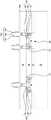
图1至图22为本揭露的部分实施例的集成电路结构在一系列制造步骤中不同阶段的示意图;1 to 22 are schematic diagrams of different stages of an integrated circuit structure in a series of manufacturing steps according to some embodiments of the disclosure;
图23为本揭露的部分实施例的集成电路结构的示意图;23 is a schematic diagram of an integrated circuit structure of some embodiments of the disclosure;
图24至图30为本揭露的部分实施例的集成电路结构在一系列制造步骤中不同阶段的示意图。24 to 30 are schematic diagrams of different stages of an integrated circuit structure in a series of manufacturing steps according to some embodiments of the disclosure.
【符号说明】【Symbol Description】
50:基板50: Substrate
54:源极/漏极区54: source/drain region
58:鳍58: Fins
60:FinFET元件60: FinFET components
62:STI区域62: STI area
64:导电栅极层64: Conductive gate layer
66:栅极介电质层66: Gate dielectric layer
68:栅极结构68: Gate structure
72:间隔物72: Spacer
73:源极/漏极接触73: Source/Drain Contacts
74:源极/漏极导电柱74: Source/drain conductive pillars
75:栅极接触75: Gate Contact
76:层间介电质层(ILD层)76: Interlayer dielectric layer (ILD layer)
78:层间介电质层(ILD层)78: Interlayer dielectric layer (ILD layer)
106:互连结构106: Interconnect Structure
1081,1082:金属化层1081 , 1082 : metallization layer
145:金属层145: metal layer
146,146A,146B,146C:导电柱插塞146, 146A, 146B, 146C: Conductive Post Plugs
150:扩散阻挡层150: Diffusion barrier
151:扩散阻挡层151: Diffusion barrier
155,155A,155B,155C:金属导电柱155, 155A, 155B, 155C: Metal Conductive Post
160,160A,160B,160C:介电质层160, 160A, 160B, 160C: Dielectric layers
160S,165S:导电柱间介电部分160S, 165S: Dielectric part between conductive pillars
165,165A,165B,165C:介电质层165, 165A, 165B, 165C: Dielectric layers
166,166A,166B,166C:金属间介电质层(IMD层)166, 166A, 166B, 166C: Intermetal dielectric layer (IMD layer)
245:金属层245: Metal Layer
246,246A,246B,246C:金属线结构246, 246A, 246B, 246C: Metal Wire Structures
251,251A,251B,251C:扩散阻挡层251, 251A, 251B, 251C: Diffusion Barriers
255,255A,255B,255C:金属线结构255, 255A, 255B, 255C: Metal Wire Structure
260,260A,260B,260C:介电质层260, 260A, 260B, 260C: Dielectric layers
265,265A,265B,265C:介电质层265, 265A, 265B, 265C: Dielectric layers
260S,265S:线间介电部分260S, 265S: Dielectric part between lines
266,266A,266B,266C:金属间介电质层(IMD层)266, 266A, 266B, 266C: Intermetal dielectric layer (IMD layer)
270:蚀刻停止层270: Etch Stop Layer
272:介电质层272: Dielectric Layer
275:金属间介电质层(IMD层)275: Intermetal dielectric layer (IMD layer)
282:阻挡层282: Barrier
284:金属层284: Metal Layer
284M:金属线部分284M: Metal wire part
284V:导电柱部分284V: Conductive column part
340:蚀刻停止层340: Etch Stop Layer
345:金属层345: Metal Layer
346:导电柱插塞346: Conductive post plug
346M:主要部分346M: Main part
346E:延伸部分346E: Extensions
351:扩散阻挡层351: Diffusion Barrier
355:金属导电柱355: Metal conductive column
360:介电质层360: Dielectric Layer
365:介电质层365: Dielectric Layer
366:金属间介电质层(IMD层)366: Intermetal dielectric layer (IMD layer)
506:互连结构506: Interconnect Structure
5081,5082,5083,5084:金属化层5081 , 5082 , 5083 , 5084 : metallization layer
H1,H2,H3,H4:高度H1,H2,H3,H4: height
R1,R2:凹槽R1, R2: groove
VO:导电柱开口VO: Conductive pillar opening
TO:沟槽开口TO: trench opening
O3:开口O3: Open
具体实施方式Detailed ways
以下揭露内容提供许多不同实施例或实例,用于实施提供的标的的不同特征。以下描述组件及配置的具体实例以简化本揭露内容。当然,此等仅为实例,且并不意欲为限制性。举例而言,在接下来的描述中,第一特征在第二特征上方或上的形成可包括第一与第二特征直接接触地形成的实施例,且亦可包括额外特征可形成于第一与第二特征之间使得第一与第二特征可不直接接触的实施例。此外,在各种实例中,本揭露内容可重复参考数字及/或字母。此重复系为了简单且清晰的目的,且自身并不规定论述的各种实施例及/或组态之间的关系。The following disclosure provides many different embodiments or examples for implementing different features of the provided subject matter. Specific examples of components and configurations are described below to simplify the present disclosure. Of course, these are only examples and are not intended to be limiting. For example, in the description that follows, the formation of a first feature over or on a second feature may include embodiments in which the first and second features are formed in direct contact, and may also include additional features that may be formed on the first feature. Embodiments in which the first and second features may not be in direct contact with the second feature. Furthermore, in various instances, the present disclosure may repeat reference numbers and/or letters. This repetition is for the purpose of simplicity and clarity, and does not in itself prescribe the relationship between the various embodiments and/or configurations discussed.
另外,为了易于描述,诸如“在……之下(beneath)”、“在……下方(below)”、“下部(lower)”、“在……上方(above)”及“上部(upper)”及类似者的空间相对术语可在本文中用以描述如在图中图示的一个元件或特征与另一元件或特征的关系。除了图中描绘的定向之外,这些空间相对术语意欲亦涵盖在使用或操作中的元件的不同定向。可将设备以其他方式定向(旋转90度或以其他定向),且同样地可将本文中使用的空间相对描述词相应地作出解释。In addition, for ease of description, such as "beneath", "below", "lower", "above" and "upper" ” and similar spatially relative terms may be used herein to describe the relationship of one element or feature to another element or feature as illustrated in the figures. In addition to the orientation depicted in the figures, these spatially relative terms are intended to encompass different orientations of the elements in use or operation. The device may be otherwise oriented (rotated 90 degrees or at other orientations), and likewise the spatially relative descriptors used herein interpreted accordingly.
图1示出了根据一些实施例的半导体基板50,其中半导体基板50上方可以形成各种电子元件。一般来说,图1所示的基板50可以包括体半导体基板或绝缘体上硅(silicon-on-insulator;SOI)基板。SOI基板包括位于作为SOI基板的主动层的薄半导体层下方的绝缘体层。主动层的半导体和体半导体通常包括晶体半导体材料硅,但也可以包括一种或多种其他半导体材料,例如锗、硅锗合金、化合物半导体(例如GaAs、AlAs、InAs、GaN、AlN)等),或它们的合金(例如,GaxAl1-xAs、GaxAl1-xN、InxGa1-xAs等)、氧化物半导体(例如,ZnO、SnO2、TiO2、Ga2O3等)或它们的组合。半导体材料可以是掺杂的或未掺杂的。亦可使用其他的基板,包括多层基板、梯度基板或混合晶向基板。1 illustrates a
鳍式场效应晶体管(FinFET)元件60设置在基板50上。在一些实施例中,图1中所示的FinFET元件60是三维MOSFET结构,形成于半导体的鳍状的条带突起可称为鳍58。图1中所示的横截面是在沿鳍状物的长轴方向截取,此方向平行于源极/漏极区54之间的电流方向。鳍58可以通过使用微影和蚀刻技术。例如,可以使用间隔物图像转移(spacer imagetransfer;SIT)图案化技术。在此方法中,牺牲层形成在基板上方并使用合适的微影和蚀刻制程图案化以形成心轴(mandrel)。使用自对准制程在心轴旁边形成间隔物。然后通过适当的选择性蚀刻制程去除牺牲层。每个剩余的间隔物可作为硬遮罩,并通过使用例如反应离子蚀刻(RIE)将沟槽蚀刻到基板50中来图案化相应的鳍58。图1示出了单个鳍片58,然而基板50可以包括任何数量的鳍片。A Fin Field Effect Transistor (FinFET)
在图1中,沿着鳍58的相对侧壁形成的浅沟槽隔离(shallow trench isolation;STI)区62。STI区62可以通过沉积一种或多种介电材料(例如,氧化硅)以完全填充沟槽并围绕鳍片,接着使介电材料的顶面凹陷而形成。STI区域62的介电材料可以使用高密度电浆化学气相沉积(HDP-CVD)、低压CVD(LPCVD)、次大气压CVD(sub-atmosphericCVD;SACVD)、可流动CVD(FCVD)、旋涂,及/或类似者,或其组合。在沉积之后,可以执行退火制程或固化制程。在一些情况下,STI区62可以包括衬垫,例如通过氧化硅表面而生长的热氧化物衬垫。凹陷制程可以使用例如平坦化制程(例如,化学机械研磨(CMP)),接着执行可以使STI区域62中的介电材料的表面的顶部凹陷的选择性蚀刻制程(例如,湿蚀刻或干蚀刻,或它们的组合),使得鳍58的上部从周围的绝缘STI区域62中突出。在一些情况下,用于形成鳍58的图案化硬遮罩也可以通过平坦化制程去除。In FIG. 1 , shallow trench isolation (STI)
在一些实施例中,图1所示的FinFET元件60的栅极结构68是可以使用后栅极制程形成的高k金属栅极(HKMG)栅极结构。在后栅极制程中,在形成STI区62之后形成牺牲虚设栅极结构(未示出)。虚设栅极结构可以包括虚设栅极介电质、虚设闸电极和硬遮罩。首先,可以沉积虚设栅极介电材料(例如,氧化硅、氮化硅等)。接下来,可以在虚设栅极介电质上方沉积虚设栅极材料(例如,非晶硅、多晶硅等),然后平坦化(例如,通过CMP)。可以在虚设栅极材料上方形成硬遮罩层(例如,氮化硅、碳化硅等)。然后通过图案化硬遮罩并使用合适的微影和蚀刻技术将该图案转移到虚设栅极介电质和虚设栅极材料来形成虚设栅极结构。虚设栅极结构可以沿着突出鳍的多侧延伸并且在STI区域62的表面上方的鳍之间延伸。如下文更详细描述的,虚设栅极结构可以由HKMG栅极结构68替换,如图中所示。图1右侧所示的HKMG栅极结构68(在鳍58的顶部)是主动HKMG栅极结构的范例。用于形成虚设栅极结构和硬遮罩的材料可以使用任何合适的方法沉积,例如CVD、电浆增强CVD(PECVD)、原子层沉积(ALD)、电浆增强ALD(PEALD)等,或通过半导体表面的热氧化,或其组合。In some embodiments, the
图1所示的FinFET 60的源极/漏极区54以及间隔物72可形成为与虚设栅极结构自对准。可以通过在完成虚设栅极图案化之后执行的间隔物介电质层的沉积和非等向性蚀刻来形成间隔物72。间隔物介电质层可包括一种或多种介电材料,例如氧化硅、氮化硅、氮氧化硅、碳化硅、碳氮化硅等,或其组合。非等向性蚀刻制程从虚设栅极结构的顶部去除间隔物介电质层,留下间隔物72沿着虚设栅极结构的侧壁横向延伸到鳍的表面的一部分上(如图中右侧所示)或STI的表面。The source/
源极/漏极区54是与半导体鳍58直接接触的半导体区。在一些实施例中,源极/漏极区54可以包括重掺杂区和相对轻掺杂的漏极延伸区,或LDD区。通常,重掺杂区使用间隔物72与虚设栅极结构隔开,而LDD区可以在形成间隔物72之前形成,因此在间隔物72下方延伸,并且在一些实施例中,进一步延伸到虚设栅极结构下方的半导体部分。LDD区可以例如通过使用离子注入制程注入掺杂剂(例如,As、P、B、In等)来形成。The source/
源极/漏极区54可以包括磊晶生长区。例如,在形成LDD区之后,可以形成间隔物72,随后可以通过蚀刻鳍形成凹槽,然后重掺杂源区和漏区可与间隔物72自对准地形成,通过沉积制程,例如选择性磊晶生长(SEG)制程在凹槽中形成晶体半导体材料,该制程可以填充凹槽,并且通常延伸超出鳍的原始表面以形成凸起的源极/漏极结构,如图1所示。半导体材料可以是元素的(例如Si、或Ge等)或合金(例如Si1-xCx或Si1-xGex等)。SEG可以使用任何合适的磊晶生长方法,例如气相/固相/液相磊晶(VPE、SPE、LPE)或金属有机CVD(MOCVD)或分子束磊晶(MBE)等。高剂量(例如,约1014cm-2至1016cm-2)的掺杂剂可以在选择性磊晶生长期间原位或通过在选择性磊晶生长之后执行的离子注入制程被引入到重掺杂源极/漏极区54中,或其组合。The source/
第一层间介电质(ILD)层76(见图1)沉积在结构上。在一些实施例中,可在沉积ILD材料之前沉积具有合适介电质(例如,氮化硅、碳化硅等或其组合)的接触蚀刻停止层(CESL)(未示出)。可执行平坦化制程(例如,CMP)以从虚设栅极上方去除多余的ILD材料和任何剩余的硬遮罩材料以形成一顶面,其中虚设栅极材料的此顶面曝露且可以与第一ILD层76的顶面实质上共面。接着,可以通过使用一种或多种蚀刻技术去除虚设栅极结构以在对应的间隔物72之间形成沟槽来形成图1所示的HKMG栅极结构68。沉积包括一种或多种介电质的替代栅极介电质层66,接着沉积包括一种或多种导电材料的替代导电栅极层64以完全填充凹槽。可以使用例如CMP制程从第一ILD层76的顶表面上方去除导电栅极层64和栅极介电质层66的多余部分。如图1所示,所得结构可以是基本共面的表面,其包括第一ILD层76的暴露顶面、间隔物72以及镶嵌在相应间隔物72之间的栅极介电质层66和导电栅极层64的剩余部分。A first interlayer dielectric (ILD) layer 76 (see FIG. 1 ) is deposited on the structure. In some embodiments, a contact etch stop layer (CESL) (not shown) with a suitable dielectric (eg, silicon nitride, silicon carbide, etc., or combinations thereof) may be deposited prior to depositing the ILD material. A planarization process (eg, CMP) may be performed to remove excess ILD material and any remaining hard mask material from over the dummy gate to form a top surface, where this top surface of the dummy gate material is exposed and can be The top surfaces of the ILD layers 76 are substantially coplanar. Next, the
源极/漏极接触73形成在第一ILD层76中并且与FinFET 60的源极/漏极区54进行电连接。源极/漏极接触73可以使用微影技术形成。例如,可以在第一ILD层76上方形成图案化遮罩并且蚀刻延伸穿过第一ILD层76和第一ILD层76下方的CESL(未示出)形成开口以暴露源极/漏极区54的部分。在一些实施例中,可以使用非等向性干蚀刻制程进行蚀刻。Source/
在一些实施例中,可以在第一ILD层76中的开口中形成导电衬垫。随后,用导电填充材料填充开口。衬垫包括用于减少导电材料从源极/漏极接触73向外扩散到周围介电材料中的金属。在一些实施例中,衬垫可以包括两个金属层。第一金属层与源极/漏极区54中的半导体材料接触,随后可与源极/漏极区54中的重掺杂半导体发生化学反应以形成低电阻欧姆接触,之后未反应的金属可能会被移除。例如,如果源极/漏极区54中的重掺杂半导体是硅或硅锗合金半导体,则第一金属层可以包括Ti、Ni、Pt、Co、其他合适的金属或它们的合金。导电衬垫的第二金属层可以另外包括其他金属(例如,TiN、TaN、Ta或其他合适的金属,或它们的合金)。可以使用任何可接受的沉积技术将导电填充材料(例如,W、Al、Cu、Ru、Ni、Co、这些的合金、它们的组合等)沉积在导电衬垫层上以填充接触开口(例如,CVD、ALD、PEALD、PECVD、PVD、ECP、化学镀等,或其任何组合)。接下来,可以使用平坦化制程(例如,CMP)从第一ILD层76的表面上方去除所有导电材料的多余部分。所得导电插塞延伸到第一ILD层76中并且构成源极/漏极接触73与电子元件的电极进行物理和电连接,例如图1中所示的FinFET元件60。In some embodiments, conductive pads may be formed in the openings in the
如图1所示,可以在第一ILD层76上方沉积第二ILD层78。在一些实施例中,形成第一ILD层76和第二ILD层78的绝缘材料可以包括氧化硅,磷硅玻璃(PSG)、硼硅玻璃(BSG)、硼掺杂磷硅玻璃(BPSG)、未掺杂硅玻璃(USG)、低介电常数(low-k)介电质,例如氟硅玻璃(FSG)、碳氧化硅(SiOCH)、碳掺杂氧化物(CDO)、可流动氧化物或多孔氧化物(例如,干凝胶/气凝胶)等,或它们的组合。用于形成第一ILD层76和第二ILD层78的介电材料可以使用任何合适的方法沉积,例如CVD、物理气相沉积(PVD)、ALD、PEALD、PECVD、SACVD、FCVD、旋涂,和/或类似物,或其组合。As shown in FIG. 1 , a
栅极介电质层66包括例如高k介电材料,例如金属的氧化物和/或硅酸盐(例如Hf、Al、Zr、La、Mg、Ba、Ti的氧化物和/或硅酸盐)、和其他金属)、氮化硅、氧化硅等,或它们的组合,或它们的多层。在一些实施例中,导电栅极层64可以是多层金属栅极堆叠,其包括在栅极介电质层66顶部连续形成的阻挡层、功函数层和栅极填充层。阻挡层的示例材料包括TiN、TaN、Ti、Ta等,或其多层组合。对于p型FET,功函数层可以包括TiN、TaN、Ru、Mo、Al,对于n型FET可以包括Ti、Ag、TaAl、TaAlC、TiAlN、TaC、TaCN、TaSiN、Mn、Zr.可以使用其他合适的功函数材料,或它们的组合,或多层。填充凹槽的其余部分的栅极填充层可以包括诸如Cu、Al、W、Co、Ru等的金属,或者它们的组合,或者它们的多层。用于形成栅极结构的材料可以通过任何合适的方法沉积,例如CVD、PECVD、PVD、ALD、PEALD、电化学镀(ECP)、化学镀等。The
如图1所示,源极/漏极导电柱74形成在第二ILD层78中并且与对应的源极/漏极接触73进行电连接。栅极接触75形成在第二ILD层78中并且分别与FinFET元件60的对应导电栅极层64电连接。栅极接触75、源极/漏极接触73和源极/漏极导电柱74可以称为中端(middle-end-of-line;MEOL)导电特征,其电连接线前端(front-end-of-line;FEOL;)导电特征(例如,栅极结构68和/或源极/漏极区54)到后端(back-end-of-line;BEOL)导电特征(例如,互连结构106中的金属导电柱和金属线,如图22所示)。栅极接触75和源极/漏极导电柱74可以使用微影技术形成。例如,可以在第二ILD层78上方形成图案化遮罩并蚀刻延伸穿过第二ILD层78形成开口以暴露STI区域62和源极/漏极接触73上方的栅极电极的一部分。在部分实施例中,可以使用非等向性干蚀刻制程来蚀刻开口。As shown in FIG. 1 , source/drain
在一些实施例中,可以在第二ILD层78中的开口中形成导电衬垫。随后,用导电填充材料填充开口。衬垫包括用于减少导电材料从栅极接触75和源极/漏极导电柱74向外扩散到周围介电材料中的金属。在一些实施例中,衬垫可以包括两个金属层。第一金属层可以包括Ti、Ni、Pt、Co、其他合适的金属或它们的合金。导电衬垫的第二金属层可以另外包括其他金属(例如,TiN、TaN、Ta或其他合适的金属,或它们的合金)。可以使用任何可接受的沉积技术(例如,CVD、ALD、PEALD、PECVD、PVD、ECP、化学镀等,或其任何组合)在导电衬垫层上沉积导电填充材料以填充接触开口.导电填充材料可以是钨(W)或其他合适的导电材料,例如Al、Cu、Ru、Ni、Co、这些的合金、它们的组合等。接下来,可以使用平坦化制程(例如,CMP)从第二ILD层78的表面上方去除所有导电材料的多余部分。所得导电插塞延伸到第二ILD层78中并且构成栅极接触75和源极/漏极导电柱74分别与导电栅极层64和源极/漏极接触73进行物理和电连接。In some embodiments, conductive pads may be formed in the openings in the
在一些实施例中,源极/漏极接触73、源极/漏极导电柱74和栅极接触75中的每一个可以包括倒梯形横截面轮廓。即,源极/漏极接触73、源极/漏极导电柱74和栅极接触75的宽度可以随着距基板50的距离增加而增加。In some embodiments, each of source/
参考图2,在ILD层78上形成金属层145。在一些实施例中,金属层145的材料可以包括铜或铜合金,或其他合适的导电材料,例如银,金、钨、铝或其他合适的材料。在一些实施例中,金属层145可以通过例如CVD、ALD、PVD等形成。Referring to FIG. 2 , a
参考图3,金属层145被图案化以形成多个导电柱插塞146。在一些实施例中,金属层145可以通过例如形成遮罩层(例如,光阻)在金属层145上,图案化遮罩层以暴露金属层145的部分,并蚀刻金属层145的暴露部分。金属层145的剩余部分被称为导电柱插塞146。在一些在实施例中,导电柱插塞146可以分别与栅极接触75和源极/漏极导电柱74接触。在一些实施例中,每个导电柱插塞146的底面可以比每个栅极接触75的顶面和/或每个源极/漏极导电柱74的顶面更宽,这将降低导电柱插塞146和对应的栅极接触75或源极/漏极导电柱74之间的电阻。在一些其他实施例中,每个导电柱插塞146的底面可以等于或窄于每个栅极接触75的顶面和/或每个源极/漏极导电柱74的顶面。Referring to FIG. 3 , the
在一些实施例中,导电柱插塞146可以包括梯形横截面轮廓。即,导电柱插塞146的宽度可以随着与基板50的距离增加而减小。换言之,导电柱插塞146的顶面比导电柱插塞146的底面窄。在一些实施例中,每个导电柱插塞146具有与ILD层78的顶面接触的底面。In some embodiments,
参考图4,扩散阻挡层150形成在基板50上方并覆盖导电柱插塞146和ILD层78。在一些实施例中,扩散阻挡层150可以以保形方式沉积,使得扩散阻挡层150可以沿着导电柱插塞146和ILD层78的暴露表面延伸。在一些实施例中,扩散阻挡层150可以包括阻挡材料,例如钛(Ti)、氮化钛(TiN)、钽(Ta)、氮化钽(TaN)及其组合,并且可以使用CVD、ALD、PVD等形成。Referring to FIG. 4 , a
参考图5A。图案化扩散阻挡层150以在每个导电柱插塞146的相对侧壁上形成扩散阻挡层151。在一些实施例中,可以通过例如非等向性蚀刻制程来图案化扩散阻挡层150以移除位于导电柱栓塞146的顶面和蚀刻停止层140的顶面的扩散阻挡层150的水平部分。在蚀刻制程之后,扩散阻挡层150的剩余部分可以称为扩散阻挡层151。如图5B所示,在部分实施例中,在导电柱插塞146为圆柱,并在上视图中具有圆形轮廓,其中扩散阻挡层151在对应的导电柱插塞146周围形成环形结构。Referring to Figure 5A. The
在形成扩散阻挡层151之后,扩散阻挡层151和相应的导电柱插塞146可以统称为金属导电柱155。在一些实施例中,每个金属导电柱155包括导电柱插塞146和内衬在导电柱插塞146相对侧壁上的扩散阻挡层151。在一些实施例中,扩散阻挡层151的底面与ILD层78接触,并且与过导电柱插塞146的底面基本齐平。After the
参考图6。介电质层160形成在金属导电柱155上方并填充金属导电柱155之间的空间。在一些实施例中,介电质层160与ILD层78的顶面接触,并与金属导电柱155的侧壁和顶面接触。更详细地说,介电质层160与扩散阻挡层151的外侧壁和顶面接触,并与导电柱插塞146的顶面接触。Refer to Figure 6. The
在一些实施例中,介电质层160可以由低k介电材料形成,例如掺氢碳氧化硅(SiOC:H)。因此,介电质层160也可称为低k介电质层。在一些实施例中,介电质层160的介电常数在约

参考图7。执行CMP制程以去除介电质层160的多余材料,直到暴露金属导电柱155。在一些实施例中,在CMP制程之后,介电质层160的顶面基本上与金属导电柱155的顶面齐平。更详细地,执行CMP制程以将介电质层160的顶面从高于金属导电柱155的顶面的位置到与金属导电柱155的顶面齐平的位置。在一些实施例中,CMP制程可省略不执行。Refer to Figure 7. A CMP process is performed to remove excess material from the
参考图8,介电质层160被回蚀刻以在金属导电柱155之间形成凹槽R1。因此,金属导电柱155的上部的侧壁被暴露。更详细地,扩散阻挡层151的上部的侧壁被暴露。Referring to FIG. 8 , the
在一些实施例中,介电质层160的顶面从与金属导电柱155的顶面齐平的位置降低到低于金属导电柱155的顶面的位置。如果图7的CMP制程被省略,则可以对图6所示的结构进行回蚀制程。在这种情况下,回蚀制程将介电质层160的顶面从高于金属导电柱155的顶面的位置降低至低于金属导电柱155的顶面的位置。In some embodiments, the top surface of the
参考图9。介电质层165形成在金属导电柱155上方并填充金属导电柱155之间的凹槽R1。在一些实施例中,介电质层165与介电质层160的顶面接触,并与金属导电柱155的侧壁和顶面接触。更详细地说,介电质层160与金属导电柱155的侧壁的上部和金属导电柱155的顶面接触。Refer to Figure 9. The
在一些实施例中,介电质层165可以包括具有比介电质层160更高的介电常数的介电材料。在介电质层165由氧化硅制成的一些实施例中,介电质层165的介电常数大约是3.9。在一些实施例中,介电质层160的碳原子百分比可高于介电质层165的碳原子百分比。另一方面,介电质层160的氧原子百分比可低于介电质层165的氧原子百分比。介电质层165可以包括氧化硅。介电质层165可以用高密度电浆CVD(HDPCVD)、PECVD、可流动CVD制程或其他合适的沉积制程沉积。In some embodiments,
参考图10。执行CMP制程以去除介电质层165的多余材料直到暴露金属导电柱155。在一些实施例中,在CMP制程之后,介电质层165的顶面实质上与金属导电柱155的顶面齐平。更详细地,执行CMP制程以将介电质层165的顶面从从高于金属导电柱155的顶面的位置降低到与金属导电柱155的顶面齐平的位置。在一些实施例中,介电质层160和165可以统称为金属间介电质(inter-metal dielectric;IMD)层166。Refer to Figure 10. A CMP process is performed to remove excess material from the
在CMP制程完成之后,介电质层160具有高度Hl而介电质层165具有高度H2。在一些实施例中,介电质层160的高度H1大于介电质层165的高度H2。换句话说,介电质层160在垂直方向上比介电质层165厚。After the CMP process is completed, the
介电质层165可以作为介电质层160的保护层。在一些实施例中,如果介电质层160暴露于蚀刻制程(例如,干蚀刻或湿蚀刻)或对金属导电柱155执行的金属处理制程,介电质层160的表面容易被破坏。通过在介电质层160上方形成介电质层165,可以保护介电质层160免受后续制程的影响,进而提高元件可靠性。例如,可以提高元件的时间相关介电质崩溃(time dependent dielectric breakdown;TDDB)和介电电压崩溃(dielectric voltagebreakdown;VBD)性能。The
在一些实施例中,介电质层165的高度H2在从大约


在一些实施例中,在完成CMP制程之后,介电质层160可以包括每个位于两个相邻金属导电柱155之间的导电柱间介电部分160S,且介电质层165可以包括每个位于两个相邻金属导电柱155之间的导电柱间介电部分165S,其中介电质层165的导电柱间介电部分165S在介电质层160的导电柱间介电部分160S之上。在一些实施例中,介电质层160的导电柱间介电部分160S与介电质层165的导电柱间介电部分165S可以包括倒梯形横截面轮廓。即,介电质层160的导电柱间介电部分160S的宽度和介电质层165的导电柱间介电部分165S的宽度可以随着距基板50的距离增加而增加。换言之,介电质层160的导电柱间介电部分160S的顶面宽于介电质层160的导电柱间介电部分160S的底面,而介电质层165的导电柱间介电部分165S的顶面宽于介电质层165的导电柱间介电部分165S的底面。在一些实施例中,介电质层165的导电柱间介电部分165S的顶面宽于介电质层160的导电柱间介电部分160S的顶面,且介电质层165的导电柱间介电部分165S的底面宽于介电质层160的导电柱间介电部分160S的底面。In some embodiments, after the CMP process is completed, the
参考图11,在介电质层165上方形成金属层245。金属层245与金属导电柱155接触。在一些实施例中,金属层245的材料可以包括铜或铜合金,或其他合适的导电材料,例如银、金、钨、铝或其他合适的材料。在一些实施例中,金属层245可以通过例如CVD、ALD、PVD等形成。Referring to FIG. 11 , a
请参考图12,对金属层245进行图案化,形成多条金属线246。金属导电柱155的维度在纵向上最长,而金属线246的维度在横向上最长,因此金属导电柱155可用于垂直传导电流并用于电连接位于垂直相邻两层的两个导电特征,而金属线246可用于横向传导电流并用于在一层内分配电讯号和电力。在一些实施例中,可以通过例如在金属层245上方形成遮罩层(例如,光阻)、图案化遮罩层以暴露金属层245的部分以及蚀刻暴露的部分来图案化金属层245。金属层245的剩余部分可称为金属线246。在一些实施例中,金属线246与对应的金属导电柱155接触。Referring to FIG. 12 , the
在一些实施例中,在蚀刻金属层245期间,介电质层165可以充当保护层以保护介电质层160,因为由SiO2制成的介电质层165比介电质层160更不容易被损坏由SiCO:H制成。在一些实施例中,蚀刻金属层245的蚀刻剂可以是NF3、CH4、C2H6、C3F8、CxHyFz。In some embodiments, the
在一些实施例中,每条金属线246可以包括梯形横截面轮廓。即,金属线246的宽度可以随着与衬底50的距离增加而减小。换言之,金属线246的顶面比金属线246的底面窄。在一些实施例中,金属线246具有与介电质层165、导电柱插塞146和扩散阻挡层接触的底面151。In some embodiments, each
参考图13,形成扩散阻挡层251每条金属线246的相对侧壁上。在一些实施例中,扩散阻挡层251可以通过下列方法形成,例如,在金属线246和介电质层165上方沉积扩散阻挡层,并执行非等向性蚀刻制程移除位在介电质层165顶面和金属线246顶面上的扩散阻挡层的水平部分。蚀刻制程后,剩余部分的扩散阻挡层可以被称为扩散阻挡层251。Referring to FIG. 13 , diffusion barrier layers 251 are formed on opposite sidewalls of each
在形成扩散阻挡层251之后,扩散阻挡层251和相对应的金属线246可以统称为金属线结构255。在一些实施例中,每个金属线结构255包括金属线246和位在金属线246的相对侧壁上的扩散阻挡层251。在一些实施例中,扩散阻挡层251的底面与介电质层165接触,且与金属线246的底面实质上齐平。在实施例中,扩散阻挡层251通过金属线246与金属导电柱155隔开。After the
参考图14,介电质层260形成在金属线结构255上方并填充金属线结构255之间的空间。在一些实施例中,介电质层260与介电质层165的顶面接触并与金属线结构255的侧壁和顶面接触。更详细地说,介电质层260与扩散阻挡层251的外侧壁和顶面接触,并与金属线246的顶面接触。Referring to FIG. 14 , a
在一些实施例中,介电质层260可以由低k介电材料形成,例如掺氢碳氧化硅(SiOC:H)。因此,介电质层260也可称为低k介电质层。在一些实施例中,介电质层260的介电常数在约2.6至约3.5的范围内。在介电质层260由掺氢碳氧化硅(SiOC:H)制成的一些实施例中,介电质层260的介电常数约为3.9。介电质层260可以用高密度电浆CVD(HDPCVD)或PECVD制程或可流动CVD制程沉积。在一些实施例中,介电质层260可以包括比介电质层165低的介电常数。In some embodiments,
参考图15,执行CMP制程以去除介电质层260的多余材料直到暴露金属线结构255。在一些实施例中,在CMP制程之后,介电质层260的顶面实质上与金属线结构255的顶面齐平。更详细地,执行CMP制程以将介电质层260的顶面从高于金属线结构255顶面的位置降低到与金属线结构255的顶面齐平的位置。在一些其他实施例中,CMP制程可以省略。Referring to FIG. 15 , a CMP process is performed to remove excess material from the
参考图16,介电质层260被回蚀以在金属线结构255之间形成凹槽R2。因此,金属线结构255的上部的侧壁被暴露。更详细而言,金属线结构255的扩散阻挡层251的上部的侧壁被暴露。Referring to FIG. 16 , the
在一些实施例中,介电质层260的顶面从与金属线结构255的顶面齐平的位置降低到低于金属线结构255顶面的位置。在图18的CMP制程被省略的实施例中,可以对图17所示的结构进行回蚀制程。在这种情况下,回蚀制程将介电质层260的顶面从高于金属线结构255顶面的位置降低至低于金属线结构255顶面的位置。In some embodiments, the top surface of the
参考图17,介电质层265形成在金属线结构255上方并填充金属线结构255之间的凹槽R2。在一些实施例中,介电质层265与介电质层260的顶面接触并与金属线结构255的顶面和侧壁接触。更详细地说,介电质层260与金属线结构255的侧壁的上部接触以及和金属线结构255的顶面接触。Referring to FIG. 17 , a
在一些实施例中,介电质层265可以包括具有比介电质层260更高的介电常数的介电材料。在介电质层265由氧化硅制成的一些实施例中,介电质层265的介电常数大约是3.9。在一些实施例中,介电质层260的碳原子百分比可高于介电质层265的碳原子百分比。另一方面,介电质层260的氧原子百分比可低于介电质层265的氧原子百分比。在一些实施例中,介电质层265可以包括氧化硅。介电质层165可以用高密度电浆CVD(HDPCVD)、PECVD、ALD、PEALD或其他合适的制程沉积。In some embodiments,
参考图18,执行CMP制程以去除介电质层265的多余材料直到暴露金属线结构255。在一些实施例中,在CMP制程之后,介电质层265的顶面实质上与金属线结构255的顶面齐平。更详细地,执行CMP制程以将介电质层265的顶面从高于金属线结构255顶面的位置降低到与金属线结构255顶面齐平的位置。在一些实施例中,介电质层260和265可以统称为金属间介电质(IMD)层266。Referring to FIG. 18, a CMP process is performed to remove excess material from the
在CMP制程完成之后,介电质层260具有高度H3而介电质层265具有高度H4。在一些实施例中,介电质层260的高度H3大于介电质层265的高度H4。换句话说,介电质层260在垂直方向上比介电质层265厚。After the CMP process is completed, the
在一些实施例中,介电质层265的高度H4在从大约


在一些实施例中,在CMP制程完成之后,介电质层260可以包括每一个在两个相邻金属线结构255之间的线间介电部分260S,而介电质层265可以包括在两个相邻的金属线结构255之间的线间介电部分265S,其中介电质层265的线间介电部分265S位于介电质层260的线间介电部分260S上方。在一些实施例中,介电质层260的线间介电部分260S和介电质层265的线间介电部分265S可以包括倒梯形横截面轮廓。即,介电质层260的线间介电部分260S的宽度和介电质层265的线间介电部分265S的宽度可以随着距基板50的距离增加而增加。换言之,介电质层260的线间介电部260S的顶面宽于介电质层260的线间介电部260S的底面,而线间介电部265S的顶面宽于介电质层265的线间介电部265S的底面。在一些实施例中,介电质层265的线间介电部分265S的顶面宽于介电质层260的线间介电部260S的顶面,且介电质层265的线间介电部265S的底面宽于介电质层260的线间介电部260S的底面。In some embodiments, after the CMP process is completed, the
参考图19。蚀刻停止层270和介电质层272形成在IMD层266上方。在一些实施例中,蚀刻停止层270包括一个或多个绝缘层(例如,SiN、SiC、SiCN、SiCO、CN、它们的组合等)且和上方的介电质层272具有不同的蚀刻速率。在一些实施例中,介电质层272可以包括氧化硅、磷硅酸盐玻璃(PSG)、硼硅酸盐玻璃(BSG)、掺硼磷硅酸盐玻璃(BPSG)、未掺杂硅酸盐玻璃(USG)、低介电常数(low-k)介电质,例如氟硅酸盐玻璃(FSG)、碳氧化硅(SiOCH)、碳掺杂氧化物(CDO)、可流动氧化物或多孔氧化物(例如,干凝胶/气凝胶)等,或它们的组合。蚀刻停止层270和介电质层272可以使用合适的方法沉积,例如CVD、物理气相沉积(PVD)、ALD、PEALD、PECVD、SACVD、FCVD、旋涂等,或其组合。在一些实施例中,蚀刻停止层270和介电质层272可统称为金属间介电质(IMD)层275。在一些实施例中,蚀刻停止层270沿垂直方向比介电质层272薄.在一些实施例中,介电质层272可以由与介电质层160和260相同的材料制成,因此介电质层272可以包括具有比介电质层160低的介电常数的介电材料。Refer to Figure 19.
参考图20,在IMD层275中形成双镶嵌开口,双镶嵌开口包括沟槽开口TO和导电柱开口VO,其中每个沟槽开口TO在一个或多个导电柱开口VO上方并与一个或多个导电柱开口VO空间连通.在一些实施例中,双镶嵌技术可以包括“先导电柱”图案化或“先沟槽”图案化,并且可以使用具有遮罩技术和非等向性的典型微影制程形成沟槽开口TO和导电柱开口VO。蚀刻操作(例如,等离子蚀刻或反应离子蚀刻)。虽然实施例绘制IMD层275中的双镶嵌开口,但也可以采用单镶嵌处理。Referring to FIG. 20, dual damascene openings are formed in the
参考图21。阻挡层282沉积在沟槽开口TO和导电柱开口VO内。金属层284沉积在在阻挡层282上方以及填充沟槽开口TO和导电柱开口VO中。在一些实施例中,阻挡层282可以包括诸如钛(Ti)、氮化钛(TiN)、钽(Ta)、氮化钽(TaN)及其组合的势垒材料,并且可以使用CVD、ALD、PVD、或类似方法形成。在一些实施例中,金属层284的材料可以包括铜或铜合金,或其他合适的导电材料,例如银、金、钨、铝或其他合适的材料,并且可以使用CVD、ALD、PVD或类似。在一些实施例中,阻挡层282可以省略。Refer to Figure 21. A
参考图22,进行CMP制程以去除阻挡层282和金属层284的多余材料。CMP制程完成后,剩余的金属层284具有在导电柱VA中的部分以及在沟槽开口TO中的部分。在一些实施例中,金属层284在导电柱开口VA中的部分可以称为导电柱部分284V,可作用为金属导电柱以在不同互连层之间垂直传导电流,而金属层284在沟槽开口TO的部分可称为金属线部分284M,其用作金属线以横向传导电流并在同一电平内分配电信号和电力。Referring to FIG. 22 , a CMP process is performed to remove excess material from the
在一些实施例中,由于不同的形成制程,金属层284的每个导电柱部分284V和金属层284的每个金属线部分284M可以包括不同于金属导电柱155和金属线结构255的横截面轮廓。例如,金属层284的导电柱部分284V和金属层284的金属线部分284M可以包括倒梯形横截面轮廓,而金属导电柱155和金属线结构255可以包括梯形截面轮廓。即,导电柱部分284V和/或金属线部分284M的宽度可以随着与基板50的距离增加而增加。换言之,导电柱部284V的顶面(或金属线部284M的顶面)比导电柱部284V的底面(或金属线部284M的底面)宽。这里,术语“导电柱部分”可以是垂直延伸的最长尺寸的部分,术语“金属线部分”可以是横向延伸的最长尺寸的部分,因此284V的导电柱部分垂直传导电流并用于电连接位于垂直相邻层的两个导电特征,而金属线部分284M横向传导电流并用于在一层内分配电信号和功率。In some embodiments, each
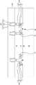
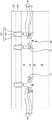
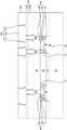
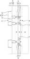
IMD层166、IMD层166中的金属导电柱155、IMD层266和IMD层266中的金属线结构255可以统称为金属化层1081。此外,IMD层275和IMD层275中的金属层284可以统称为金属化层1081上方的另一金属化层1082。可以理解,如上所述,金属化层1081和金属化层1082由不同的方式所形成。
金属化层1081和1082是互连结构106的一部分。在一些实施例中,互连结构106可以包括设置在金属化层1082之上的更多金属化层,而可以通过图19至图22所描述的方法在金属化层1082上方形成更多的金属化层,且此方法不同于图2至图18所描述用于形成金属化层1081的方法。互连结构106的形成可被称为后端(BEOL)制程。Metallization layers 1081 and 1082 are part of
图23是根据本揭露的实施例的集成电路结构。图23中讨论的部分元件与图1至图22中所讨论的相同,这些元件使用相同的元件符号,且为简单起见,不再重复相关细节。图23的结构与图22的结构的区别在于,图23的结构包括互连结构506,其中互连结构506包括金属化层5081至5084。在一些实施例中,每个金属化层5081、5082和5083类似于图22中讨论的金属化层1081,且可以通过图2至图18所讨论用于形成金属化层1081的类似方法来形成。金属化层5084类似于图22中讨论的金属化层1082,并且可以通过图19至图22用于形成金属化层1082的类似方法来形成。23 is an integrated circuit structure according to an embodiment of the present disclosure. Some of the elements discussed in Figure 23 are the same as those discussed in Figures 1-22, the same reference numerals are used for these elements, and for the sake of simplicity, the relevant details are not repeated. The structure of FIG. 23 differs from the structure of FIG. 22 in that the structure of FIG. 23 includes an
例如,金属化层5081包括IMD层166A,其包括介电质层160A和介电质层160A上方的介电质层165A。金属导电柱155A设置在IMD层166A中,并且每个金属导电柱155A包括导电柱插塞146A和在导电柱插塞146A的相对侧壁上的扩散阻挡层151A。金属化层5081还包括IMD层166A上方的IMD层266A,其包括介电质层260A和介电质层260A上方的介电质层265A。金属线结构255A设置于IMD层266A中,且每一金属线结构255A包括金属线246A及位于金属线246A的相对侧壁上的扩散阻挡层251A。For example, metallization layer5081 includes
金属化层5082包括IMD层166B,其包括介电质层160B和介电质层160B上方的介电质层165B。金属导电柱155B设置在IMD层166B中,并且每个金属导电柱155B包括导电柱插塞146B和在导电柱插塞146B的相对侧壁上的扩散阻挡层151B。金属化层5082还包括IMD层166B上方的IMD层266B,其包括介电质层260B和介电质层260B上方的介电质层265B。金属线结构255B设置在IMD层266B中,每个金属线结构255B包括金属线246B和位于金属线246B相对侧壁上的扩散阻挡层251B。Metallization layer5082 includes
金属化层5083包括IMD层166C,其包括介电质层160C和介电质层160C上方的介电质层165C。金属导电柱155C设置在IMD层166C中,并且每个金属导电柱155C包括导电柱插塞146C和在导电柱插塞146C的相对侧壁上的扩散阻挡层151C。金属化层5083还包括IMD层166C上方的IMD层266C,其包括介电质层260C和介电质层260C上方的介电质层265C。金属线结构255C设置在IMD层266C中,并且每个金属线结构255C包括金属线246C和在金属线246C的相对侧壁上的扩散阻挡层251C。
可以理解的是,如上方所讨论,金属化层5081、5082和5083是通过类似的制程形成的(如上方于图2至图18所讨论的),然而金属化层5084是通过与形成金属化层5081、5082和5083不同的方法所形成。It will be appreciated that, as discussed above, metallization layers508i , 5082, and5083 are formed by similar processes (as discussed above with respect to Figures2-18 ), whereas metallization layer5084 is formed by It is formed by a different method than forming the metallization layers 5081 , 5082 and 5083 .
在一些实施例中,互连结构506可以包括设置在金属化层5084之上的更多金属化层,而可通过如图19至图22所讨论的方法来形成金属化层5084上方的更多的金属化层,且此方法不同于图2至图18所讨论的形成金属化层5081、5082和5083的方法。互连结构506的形成可称为后端(BEOL)制程。In some embodiments,
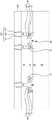
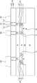
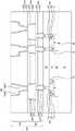
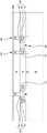
图24至图30为本揭露的部分实施例的集成电路结构在一系列制造步骤中不同阶段的示意图。图24至图30中讨论的实施例不同于图1至图22讨论的实施例。但应注意,图24至图30中讨论的部分元件与图1至图22讨论的元件相同,这些元件具有相同元件符号,且为简单起见,相关细节不再赘述。24 to 30 are schematic diagrams of different stages of an integrated circuit structure in a series of manufacturing steps according to some embodiments of the disclosure. The embodiments discussed in Figures 24-30 differ from the embodiments discussed in Figures 1-22. However, it should be noted that some elements discussed in FIGS. 24 to 30 are the same as those discussed in FIGS. 1 to 22 , these elements have the same reference numerals, and for the sake of simplicity, the relevant details are not repeated.
参考图24。蚀刻停止层340形成在ILD层78上方。在一些实施例中,蚀刻停止层340由SiN、SiCN、SiC、SiOCN等形成。在一些实施例中,蚀刻停止层340可以通过例如PECVD、ALD、CVD等形成。See Figure 24.
参考图25,蚀刻停止层340被图案化以在蚀刻停止层340中形成暴露源极/漏极导电柱74的开口O3。在一些实施例中,开口O3可以通过例如形成蚀刻停止层340上方的遮罩层(例如,光阻),图案化遮罩层以暴露蚀刻停止层340的部分,以及蚀刻蚀刻停止层340的暴露部分以形成开口O3。Referring to FIG. 25 , the
参考图26,在蚀刻停止层340上方形成金属层345并过填充蚀刻停止层340的开口O3。在一些实施例中,金属层345的材料可以包括铜或铜合金或其他合适的导电材料,例如银、金、钨、铝或其他合适的材料。在一些实施例中,金属层345可以通过例如CVD、ALD、PVD等形成。Referring to FIG. 26 , a
参考图27,金属层345被图案化以形成多个导电柱插塞346。在一些实施例中,金属层345可以通过例如形成遮罩层(例如,光阻)在金属层345上方,图案化遮罩层以暴露金属层345的部分,并且蚀刻金属层345的暴露部分。金属层345的剩余部分可称为导电柱插塞346。Referring to FIG. 27 , the
在一些实施例中,每个导电柱插塞346可以包括主要部分346M和延伸部分346E。在一些实施例中,主要部分346M是导电柱插塞346的在蚀刻停止层340的顶表面上方的部分,并且延伸部分346E是导电柱插塞346的延伸穿过蚀刻停止层340的部分。换句话说,导电柱插塞346的延伸部分346E从导电柱插塞346的主要部分346M的底部向下延伸到蚀刻停止层340中并且进一步与源极/漏极导电柱74接触。In some embodiments, each
在一些实施例中,导电柱插塞346的主要部分346M可以包括梯形截面轮廓。即,导电柱插塞346的主要部分346M的宽度可以随着距基板50的距离增加而减小。换言之,导电柱插塞346的主要部分346M的顶面比导电柱插塞346的主要部分346M的底面窄。在一些实施例中,导电柱插塞346的主要部分346M的底表面与蚀刻停止层340的顶面接触。In some embodiments, the
参考图28。扩散阻挡层351形成在每个导电柱插塞346的相对侧壁上。扩散阻挡层351可以类似于图1至图22讨论的扩散阻挡层151,且可以通过与图4至图5A中描述用于形成扩散阻挡层151的类似方法来形成。Refer to Figure 28. Diffusion barrier layers 351 are formed on opposite sidewalls of each
在形成扩散阻挡层351之后,扩散阻挡层351和相应的导电柱插塞346可以统称为金属导电柱355。在一些实施例中,每个金属导电柱355包括导电柱插塞346和导电柱插塞346的主要部分346M的相对侧壁上的扩散阻挡层351。在一些实施例中,扩散阻挡层351的底表面与蚀刻停止层340接触,并且与导电柱插塞346的主要部分346M的底表面实质上齐平。在一些实施例中,扩散阻挡层351的底面高于导电柱插塞346的延伸部分346E的底面。After the
在一些实施例中,每个金属导电柱355具有主要部分和从主要部分向下延伸的延伸部分。例如,导电柱插塞346的主要部分346M和导电柱插塞346的主要部分346M的相对侧上的扩散阻挡层351可以共同作为金属导电柱355的主要部分,而导电柱栓塞346的延伸部分346E可以作为金属导电柱355的延伸部分。在一些实施例中,金属导电柱355的延伸部分不具有扩散阻挡层351的材料。In some embodiments, each metal
在一些实施例中,金属导电柱355的主要部分可以包括梯形截面轮廓。即,金属导电柱355的主要部分346M的宽度可以随着与基板50的距离增加而减小。换言之,金属导电柱355的主要部分的顶面比金属导电柱355的主要部分的底面窄。In some embodiments, a major portion of the metal
参考图29,介电质层360和介电质层365形成在蚀刻停止层340上方,并且横向围绕金属导电柱355。介电质层360和介电质层365类似于图1至图22讨论的介电质层160和介电质层165,并且可以通过图6至图10所讨论形成介电质层160和介电质层165的方法形成。在一些实施例中,蚀刻停止层340、介电质层360和介电质层365可统称为金属间介电质(IMD)层366。Referring to FIG. 29 , a
在一些实施例中,图29的结构可以经历图11和图22所描述的制程,而结果如图30所示。图30的结构与图22的结构相似,图30的结构与图22的结构的不同之处在于图30的金属化层1081包括IMD层366和金属导电柱355。In some embodiments, the structure of FIG. 29 may undergo the process described in FIGS. 11 and 22 , and the results are shown in FIG. 30 . The structure of FIG. 30 is similar to the structure of FIG. 22 , and the difference between the structure of FIG. 30 and the structure of FIG. 22 is that the
在一些实施例中,互连结构106可以包括设置在金属化层1082之上的更多金属化层,而可以通过图19至图22所描述的方法在金属化层1082上方形成更多的金属化层,且此方法不同于图2至图18所描述用于形成金属化层1081的方法。互连结构106的形成可被称为后端(BEOL)制程。In some embodiments,
根据上述实施例,可以看出本公开在制造集成电路方面具有优势。然而,应当理解,其他实施例可以提供额外的优点,并且并非所有优点都必须在本文中公开,并且所有实施例都不需要特别的优点。一个优点是通过在低k介电质层上形成具有介电质层的IMD层,可以在一些制程中保护低k介电质层,例如蚀刻制程或金属前处理,进而提高元件的可靠度和性能。比如可以提高设备的TDDB和VBD性能。From the above-described embodiments, it can be seen that the present disclosure has advantages in manufacturing integrated circuits. It should be understood, however, that other embodiments may provide additional advantages, and that not all advantages are necessarily disclosed herein, and that no particular advantage is required for all embodiments. One advantage is that by forming an IMD layer with a dielectric layer on the low-k dielectric layer, the low-k dielectric layer can be protected during some processes, such as etching processes or metal pretreatment, thereby improving device reliability and reliability. performance. For example, the TDDB and VBD performance of the device can be improved.
在本揭露的部分实施例中,一种集成电路结构,包含基板、晶体管、第一介电质层、金属接触、第一低k介电质层、第二介电质层、第一金属特征。晶体管位于基板上方。第一介电质层位于晶体管上方。金属接触位于第一介电质层内并与晶体管电连接。第一低k介电质层位于第一介电质层上方。第二介电质层位于第一低k介电质层且第二介电质层的一介电常数高于第一低k介电质层的一介电常数。第一金属特征延伸穿越第二介电质层和第一低k介电质层至金属接触。In some embodiments of the present disclosure, an integrated circuit structure includes a substrate, a transistor, a first dielectric layer, metal contacts, a first low-k dielectric layer, a second dielectric layer, and a first metal feature . The transistors are located above the substrate. The first dielectric layer is over the transistor. A metal contact is located within the first dielectric layer and is electrically connected to the transistor. A first low-k dielectric layer is located over the first dielectric layer. The second dielectric layer is located on the first low-k dielectric layer, and a dielectric constant of the second dielectric layer is higher than a dielectric constant of the first low-k dielectric layer. The first metal feature extends through the second dielectric layer and the first low-k dielectric layer to the metal contact.
在部分实施例中,其中第一金属特征的宽度随着距离基板距离增加而减少,而金属接触的宽度随着距离基板距离增加而增加。In some embodiments, the width of the first metal feature decreases with distance from the substrate, and the width of the metal contact increases with distance from the substrate.
在部分实施例中,还包含第二低k介电质层、第三介电质层、第二金属特征。第二低k介电质层位于第二介电质层上方。第三介电质层位于第二低k介电质层上方且第三介电质层的介电常数高于第二低k介电质层的介电常数。第二金属特征位于第二低k介电质层和第三介电质层内并与第一金属特征电连接。In some embodiments, a second low-k dielectric layer, a third dielectric layer, and a second metal feature are further included. A second low-k dielectric layer is located over the second dielectric layer. The third dielectric layer is located above the second low-k dielectric layer and the dielectric constant of the third dielectric layer is higher than the dielectric constant of the second low-k dielectric layer. The second metal feature is located within the second low-k dielectric layer and the third dielectric layer and is electrically connected to the first metal feature.
在部分实施例中,其中第二低k介电质层和第二介电质层接触。In some embodiments, the second low-k dielectric layer is in contact with the second dielectric layer.
在部分实施例中,还包含第四介电质层,位于第三介电质层上方,以及双镶嵌结构,位于第四介电质层内。In some embodiments, a fourth dielectric layer is further included, located above the third dielectric layer, and a dual damascene structure is located in the fourth dielectric layer.
在部分实施例中,其中双镶嵌结构具有沿着第一方向递减的宽度,而第一金属特征具有随着第二方向递减的宽度,第二方向相反于第一方向。In some embodiments, the dual damascene structure has a decreasing width along a first direction, and the first metal feature has a decreasing width with a second direction opposite to the first direction.
在部分实施例中,还包含蚀刻停止层,位于第四介电质层和第三介电质层之间。In some embodiments, an etch stop layer is further included between the fourth dielectric layer and the third dielectric layer.
在部分实施例中,其中第一金属特征包含金属柱插塞和位于金属柱插塞的相对侧壁上的多个扩散阻挡层,且金属柱插塞接触金属接触。In some embodiments, wherein the first metal feature includes a metal stud plug and a plurality of diffusion barrier layers on opposite sidewalls of the metal stud plug, and the metal stud plug contacts the metal contact.
在部分实施例中,还包含蚀刻停止层,位于第一低k介电质层和第一介电质层之间。In some embodiments, an etch stop layer is further included between the first low-k dielectric layer and the first dielectric layer.
在部分实施例中,其中第一金属特征包含主要部分和位于主要部分下方的延伸部分,主要部分嵌入在第一低k介电质层中,延伸部分嵌入在蚀刻停止层中,且延伸部分的侧壁侧向地自主要部分的侧壁内退。In some embodiments, wherein the first metal feature includes a main portion and an extension portion underlying the main portion, the main portion is embedded in the first low-k dielectric layer, the extension portion is embedded in the etch stop layer, and the extension portion is embedded in the etch stop layer. The side walls are laterally set back from the side walls of the main portion.
在本揭露的部分实施例中,一种集成电路结构,包含基板、栅极结构、源/漏极区域、源/漏极接触、栅极接触、源/漏极导电柱、第一金属特征、第二金属特征、第一低k介电质层、第一介电质层。栅极结构位于基板上方。源/漏极区域位于基板上方且位于栅极结构的两侧。源/漏极接触位于源/漏极区域的其中一者上方。栅极接触位于栅极结构上方。源/漏极导电柱位于源/漏极接触上方。第一金属特征位于栅极接触上方。第二金属特征位于源/漏极导电柱上方。第一低k介电质层侧向地围绕第一金属特征和第二金属特征。第一介电质层侧向地围绕第一金属特征和第二金属特征且位于第一低k介电质层上方,其中第一介电质层具有比第一低k介电质层更高的介电常数和更小的厚度。In some embodiments of the present disclosure, an integrated circuit structure includes a substrate, a gate structure, source/drain regions, source/drain contacts, gate contacts, source/drain conductive pillars, first metal features, A second metal feature, a first low-k dielectric layer, a first dielectric layer. The gate structure is over the substrate. The source/drain regions are located above the substrate and on both sides of the gate structure. A source/drain contact is located over one of the source/drain regions. The gate contact is over the gate structure. Source/drain conductive pillars are located over the source/drain contacts. The first metal feature is over the gate contact. The second metal features are over the source/drain conductive pillars. The first low-k dielectric layer laterally surrounds the first metal feature and the second metal feature. The first dielectric layer laterally surrounds the first metal feature and the second metal feature and overlies the first low-k dielectric layer, wherein the first dielectric layer has a higher level than the first low-k dielectric layer dielectric constant and smaller thickness.
在部分实施例中,其中第一金属特征包含导电柱插塞和位于导电柱插塞的相对侧壁上的多个扩散阻挡层,以及扩散阻挡层的底表面与第一低k介电质层的底表面实质上齐平。In some embodiments, the first metal features include conductive pillar plugs and a plurality of diffusion barrier layers on opposite sidewalls of the conductive pillar plugs, and a bottom surface of the diffusion barrier layers and the first low-k dielectric layer The bottom surface is substantially flush.
在部分实施例中,其中导电柱插塞的底表面不具有扩散阻挡层。In some embodiments, the bottom surface of the conductive post plug does not have a diffusion barrier layer.
在部分实施例中,其中第一介电质层的上表面与第一金属特征和第二金属特征的上表面实质上齐平。In some embodiments, the upper surface of the first dielectric layer is substantially flush with the upper surfaces of the first and second metal features.
在部分实施例中,其中第一介电质层为氧化硅。In some embodiments, the first dielectric layer is silicon oxide.
在本揭露的部分实施例中,一种方法,包含在基板上形成晶体管;在晶体管上方形成层间介电质层;沉积金属层于层间介电质层上方;图案化金属层以形成金属特征;沉积低k介电质层于层间介电质层和金属特征上方;回蚀刻低k介电质层以降低低k介电质层的上表面至低于金属特征的上表面的位置;沉积介电质层于低k介电质层和金属特征上方;以及对介电质层执行第一化学机械研磨制程直到金属特征暴露。In some embodiments of the present disclosure, a method includes forming transistors on a substrate; forming an interlayer dielectric layer over the transistors; depositing a metal layer over the interlayer dielectric layer; patterning the metal layer to form a metal layer features; depositing a low-k dielectric layer over the interlayer dielectric layer and metal features; etching back the low-k dielectric layer to lower the top surface of the low-k dielectric layer to a location below the top surface of the metal features ; depositing a dielectric layer over the low-k dielectric layer and the metal features; and performing a first chemical mechanical polishing process on the dielectric layer until the metal features are exposed.
在部分实施例中,还包含沉积扩散阻挡层于层间介电质层和金属特征上方;以及移除扩散阻挡层的水平部分以暴露层间介电质层的上表面和金属特征的上表面。In some embodiments, further comprising depositing a diffusion barrier layer over the interlayer dielectric layer and the metal features; and removing a horizontal portion of the diffusion barrier layer to expose an upper surface of the interlayer dielectric layer and an upper surface of the metal features .
在部分实施例中,还包含在回蚀刻低k介电质层之前对低k介电质层执行第二化学机械研磨制程。In some embodiments, the method further includes performing a second chemical mechanical polishing process on the low-k dielectric layer before etching back the low-k dielectric layer.
在部分实施例中,其中在执行完第一化学机械研磨制程之后,介电质层较低k介电质层薄。In some embodiments, the lower-k dielectric layer of the dielectric layer is thin after the first CMP process is performed.
在部分实施例中,还包含在形成金属层之前,形成蚀刻停止层于层间介电质层上方;以及在沉积金属层之前,图案化蚀刻停止层以在蚀刻停止层内形成开口,其中金属层沉积至蚀刻停止层的开口内。In some embodiments, before forming the metal layer, forming an etch stop layer over the interlayer dielectric layer; and before depositing the metal layer, patterning the etch stop layer to form openings in the etch stop layer, wherein the metal layer layer is deposited into the openings of the etch stop layer.
前文概括了若干实施例的特征,使得熟悉此项技术者可更好地理解本揭露内容的态样。熟悉此项技术者应了解,其可易于将本揭露内容用作用于设计或修改其他处理程序及结构以用于实行相同目的及/或达成本文中介绍的实施例的相同优势的基础。熟悉此项技术者亦应认识到,此等等效构造不脱离本揭露内容的精神及范畴,且在不脱离本揭露内容的精神及范畴的情况下,其可进行各种改变、取代及更改。The foregoing summarizes features of several embodiments so that those skilled in the art may better understand aspects of the present disclosure. Those skilled in the art will appreciate that they may readily use the present disclosure as a basis for designing or modifying other processes and structures for carrying out the same purposes and/or achieving the same advantages of the embodiments presented herein. Those skilled in the art should also realize that these equivalent constructions do not depart from the spirit and scope of the present disclosure, and that various changes, substitutions and alterations may be made therein without departing from the spirit and scope of the present disclosure .
Claims (10)
Applications Claiming Priority (4)
| Application Number | Priority Date | Filing Date | Title |
|---|---|---|---|
| US202163185084P | 2021-05-06 | 2021-05-06 | |
| US63/185,084 | 2021-05-06 | ||
| US17/492,423US12278176B2 (en) | 2021-05-06 | 2021-10-01 | Integrated circuit structure and method for forming the same |
| US17/492,423 | 2021-10-01 |
Publications (1)
| Publication Number | Publication Date |
|---|---|
| CN115000015Atrue CN115000015A (en) | 2022-09-02 |
Family
ID=83023614
Family Applications (1)
| Application Number | Title | Priority Date | Filing Date |
|---|---|---|---|
| CN202210152098.7APendingCN115000015A (en) | 2021-05-06 | 2022-02-18 | Integrated circuit structure and method of forming the same |
Country Status (3)
| Country | Link |
|---|---|
| US (2) | US12278176B2 (en) |
| CN (1) | CN115000015A (en) |
| TW (1) | TW202245013A (en) |
Families Citing this family (1)
| Publication number | Priority date | Publication date | Assignee | Title |
|---|---|---|---|---|
| US20230352400A1 (en)* | 2022-04-28 | 2023-11-02 | Samsung Electronics Co., Ltd. | Integrated circuit devices including via structures having a narrow upper portion, and related fabrication methods |
Family Cites Families (14)
| Publication number | Priority date | Publication date | Assignee | Title |
|---|---|---|---|---|
| US6331481B1 (en)* | 1999-01-04 | 2001-12-18 | International Business Machines Corporation | Damascene etchback for low ε dielectric |
| JP2009123743A (en)* | 2007-11-12 | 2009-06-04 | Panasonic Corp | Manufacturing method of semiconductor device |
| US7955964B2 (en)* | 2008-05-14 | 2011-06-07 | Taiwan Semiconductor Manufacturing Company, Ltd. | Dishing-free gap-filling with multiple CMPs |
| US7928003B2 (en)* | 2008-10-10 | 2011-04-19 | Applied Materials, Inc. | Air gap interconnects using carbon-based films |
| US8518818B2 (en)* | 2011-09-16 | 2013-08-27 | Taiwan Semiconductor Manufacturing Co., Ltd. | Reverse damascene process |
| US9373586B2 (en)* | 2012-11-14 | 2016-06-21 | Taiwan Semiconductor Manufacturing Co., Ltd. | Copper etching integration scheme |
| US8728936B1 (en)* | 2012-11-14 | 2014-05-20 | Taiwan Semiconductor Manufacturing Co. Ltd. | Copper etching integration scheme |
| US10269634B2 (en)* | 2013-11-15 | 2019-04-23 | Taiwan Semiconductor Manufacturing Company, Ltd. | Semiconductor device having voids and method of forming same |
| KR102092863B1 (en)* | 2013-12-30 | 2020-03-24 | 삼성전자주식회사 | Semiconductor device and method of fabricating the same |
| US10032711B2 (en)* | 2016-07-25 | 2018-07-24 | International Business Machines Corporation | Integrating metal-insulator-metal capacitors with air gap process flow |
| US9892961B1 (en)* | 2016-08-09 | 2018-02-13 | International Business Machines Corporation | Air gap spacer formation for nano-scale semiconductor devices |
| US10535560B2 (en)* | 2017-07-18 | 2020-01-14 | Taiwan Semiconductor Manufacturing Co., Ltd. | Interconnection structure of semiconductor device |
| US10224242B1 (en)* | 2017-11-14 | 2019-03-05 | International Business Machines Corporation | Low-resistivity metallic interconnect structures |
| US11450563B2 (en)* | 2020-04-29 | 2022-09-20 | Taiwan Semiconductor Manufacturing Co., Ltd. | Interconnect structure and method |
- 2021
- 2021-10-01USUS17/492,423patent/US12278176B2/enactiveActive
- 2022
- 2022-02-18CNCN202210152098.7Apatent/CN115000015A/enactivePending
- 2022-02-25TWTW111107199Apatent/TW202245013A/enunknown
- 2024
- 2024-07-30USUS18/789,382patent/US20240395699A1/enactivePending
Also Published As
| Publication number | Publication date |
|---|---|
| US20240395699A1 (en) | 2024-11-28 |
| US20220359376A1 (en) | 2022-11-10 |
| US12278176B2 (en) | 2025-04-15 |
| TW202245013A (en) | 2022-11-16 |
Similar Documents
| Publication | Publication Date | Title |
|---|---|---|
| US10269621B2 (en) | Contact plugs and methods forming same | |
| US11450563B2 (en) | Interconnect structure and method | |
| US20240397730A1 (en) | Ferroelectric Device and Methods of Fabrication Thereof | |
| US20240413087A1 (en) | Interconnect Structure and Method of Forming Thereof | |
| US20240387372A1 (en) | Semiconductor device and method of forming thereof | |
| US20240170397A1 (en) | Interconnect level with high resistance layer and method of forming the same | |
| US20220319922A1 (en) | Self-Aligned Scheme for Semiconductor Device and Method of Forming the Same | |
| US20240395699A1 (en) | Integrated circuit structure and method for forming the same | |
| US20240363402A1 (en) | Interconnect structure and method | |
| US20250087532A1 (en) | Semiconductor device and method for forming the same | |
| US12432975B2 (en) | Semiconductor device with backside power rail | |
| US12347748B2 (en) | Semiconductor device and method of manufacturing the same | |
| US20240282772A1 (en) | NFET and PFET with Different Fin Numbers in FinFET Based CFET | |
| US20240395608A1 (en) | Glue layer etching for improving device performance and providing contact isolation | |
| US20230039661A1 (en) | Interconnect structure and methods of forming the same | |
| US20230402277A1 (en) | Semiconductor structure and manufacturing method thereof |
Legal Events
| Date | Code | Title | Description |
|---|---|---|---|
| PB01 | Publication | ||
| PB01 | Publication | ||
| WD01 | Invention patent application deemed withdrawn after publication | ||
| WD01 | Invention patent application deemed withdrawn after publication | Application publication date:20220902 |