CN114988462B - Method for preparing perovskite micron sheet with multi-wavelength emission based on chemical vapor deposition method - Google Patents
Method for preparing perovskite micron sheet with multi-wavelength emission based on chemical vapor deposition methodDownload PDFInfo
- Publication number
- CN114988462B CN114988462BCN202210574231.8ACN202210574231ACN114988462BCN 114988462 BCN114988462 BCN 114988462BCN 202210574231 ACN202210574231 ACN 202210574231ACN 114988462 BCN114988462 BCN 114988462B
- Authority
- CN
- China
- Prior art keywords
- perovskite
- temperature
- emission
- microsheets
- doped
- Prior art date
- Legal status (The legal status is an assumption and is not a legal conclusion. Google has not performed a legal analysis and makes no representation as to the accuracy of the status listed.)
- Active
Links
- 238000000034methodMethods0.000titleclaimsabstractdescription33
- 238000005229chemical vapour depositionMethods0.000titleclaimsabstractdescription18
- 238000000151depositionMethods0.000claimsdescription26
- 230000008021depositionEffects0.000claimsdescription26
- 238000010438heat treatmentMethods0.000claimsdescription25
- 239000000758substrateSubstances0.000claimsdescription24
- 229910004298SiO 2Inorganic materials0.000claimsdescription21
- VYPSYNLAJGMNEJ-UHFFFAOYSA-Nsilicon dioxideInorganic materialsO=[Si]=OVYPSYNLAJGMNEJ-UHFFFAOYSA-N0.000claimsdescription18
- LYQFWZFBNBDLEO-UHFFFAOYSA-Mcaesium bromideChemical compound[Br-].[Cs+]LYQFWZFBNBDLEO-UHFFFAOYSA-M0.000claimsdescription17
- HWSZZLVAJGOAAY-UHFFFAOYSA-Llead(II) chlorideChemical compoundCl[Pb]ClHWSZZLVAJGOAAY-UHFFFAOYSA-L0.000claimsdescription17
- HDGGAKOVUDZYES-UHFFFAOYSA-Kerbium(iii) chlorideChemical compoundCl[Er](Cl)ClHDGGAKOVUDZYES-UHFFFAOYSA-K0.000claimsdescription16
- 239000011261inert gasSubstances0.000claimsdescription16
- 239000010453quartzSubstances0.000claimsdescription16
- 239000000843powderSubstances0.000claimsdescription11
- 230000003595spectral effectEffects0.000claimsdescription11
- 238000000295emission spectrumMethods0.000claimsdescription9
- 238000001228spectrumMethods0.000claimsdescription9
- 239000011812mixed powderSubstances0.000claimsdescription8
- 238000006243chemical reactionMethods0.000claimsdescription5
- 238000005201scrubbingMethods0.000claimsdescription4
- 238000007789sealingMethods0.000claimsdescription4
- 239000012300argon atmosphereSubstances0.000claimsdescription3
- JTCFNJXQEFODHE-UHFFFAOYSA-N[Ca].[Ti]Chemical compound[Ca].[Ti]JTCFNJXQEFODHE-UHFFFAOYSA-N0.000claims2
- 125000006850spacer groupChemical group0.000claims1
- 239000000463materialSubstances0.000abstractdescription16
- 238000002360preparation methodMethods0.000abstractdescription13
- 230000003287optical effectEffects0.000abstractdescription7
- 229910052761rare earth metalInorganic materials0.000abstractdescription3
- 239000000126substanceSubstances0.000abstract1
- 235000012431wafersNutrition0.000description18
- 235000012239silicon dioxideNutrition0.000description15
- 230000000052comparative effectEffects0.000description10
- 239000012159carrier gasSubstances0.000description9
- 239000013078crystalSubstances0.000description6
- 150000004820halidesChemical class0.000description6
- XKRFYHLGVUSROY-UHFFFAOYSA-NArgonChemical compound[Ar]XKRFYHLGVUSROY-UHFFFAOYSA-N0.000description4
- 239000007789gasSubstances0.000description4
- 238000001748luminescence spectrumMethods0.000description3
- 238000004020luminiscence typeMethods0.000description3
- 230000006911nucleationEffects0.000description3
- 238000010899nucleationMethods0.000description3
- 239000004065semiconductorSubstances0.000description3
- 229910052786argonInorganic materials0.000description2
- -1cesium lead halideChemical class0.000description2
- 238000010586diagramMethods0.000description2
- 239000000203mixtureSubstances0.000description2
- 125000000962organic groupChemical group0.000description2
- 238000005070samplingMethods0.000description2
- 238000003756stirringMethods0.000description2
- 150000000917ErbiumChemical class0.000description1
- 229910052691ErbiumInorganic materials0.000description1
- PWHULOQIROXLJO-UHFFFAOYSA-NManganeseChemical compound[Mn]PWHULOQIROXLJO-UHFFFAOYSA-N0.000description1
- XUIMIQQOPSSXEZ-UHFFFAOYSA-NSiliconChemical compound[Si]XUIMIQQOPSSXEZ-UHFFFAOYSA-N0.000description1
- RTAQQCXQSZGOHL-UHFFFAOYSA-NTitaniumChemical compound[Ti]RTAQQCXQSZGOHL-UHFFFAOYSA-N0.000description1
- 239000012298atmosphereSubstances0.000description1
- QVGXLLKOCUKJST-UHFFFAOYSA-Natomic oxygenChemical compound[O]QVGXLLKOCUKJST-UHFFFAOYSA-N0.000description1
- 230000009286beneficial effectEffects0.000description1
- 230000015572biosynthetic processEffects0.000description1
- 229910052792caesiumInorganic materials0.000description1
- TVFDJXOCXUVLDH-UHFFFAOYSA-Ncaesium atomChemical compound[Cs]TVFDJXOCXUVLDH-UHFFFAOYSA-N0.000description1
- 230000007547defectEffects0.000description1
- 238000011161developmentMethods0.000description1
- 238000009792diffusion processMethods0.000description1
- UYAHIZSMUZPPFV-UHFFFAOYSA-NerbiumChemical compound[Er]UYAHIZSMUZPPFV-UHFFFAOYSA-N0.000description1
- 239000012535impuritySubstances0.000description1
- 229910052500inorganic mineralInorganic materials0.000description1
- 150000002500ionsChemical class0.000description1
- 230000001788irregularEffects0.000description1
- 230000031700light absorptionEffects0.000description1
- 229910052748manganeseInorganic materials0.000description1
- 239000011572manganeseSubstances0.000description1
- 230000008018meltingEffects0.000description1
- 238000002844meltingMethods0.000description1
- 239000010445micaSubstances0.000description1
- 229910052618mica groupInorganic materials0.000description1
- 239000011707mineralSubstances0.000description1
- 238000002156mixingMethods0.000description1
- 229910021421monocrystalline siliconInorganic materials0.000description1
- 230000005693optoelectronicsEffects0.000description1
- 239000001301oxygenSubstances0.000description1
- 229910052760oxygenInorganic materials0.000description1
- 239000002245particleSubstances0.000description1
- 238000005191phase separationMethods0.000description1
- 230000000704physical effectEffects0.000description1
- 229910052573porcelainInorganic materials0.000description1
- 238000006862quantum yield reactionMethods0.000description1
- 238000012827research and developmentMethods0.000description1
- 239000010703siliconSubstances0.000description1
- 239000000377silicon dioxideSubstances0.000description1
- 229910052814silicon oxideInorganic materials0.000description1
- 238000003786synthesis reactionMethods0.000description1
- 229910052719titaniumInorganic materials0.000description1
- 239000010936titaniumSubstances0.000description1
- 230000007704transitionEffects0.000description1
- XLYOFNOQVPJJNP-UHFFFAOYSA-NwaterSubstancesOXLYOFNOQVPJJNP-UHFFFAOYSA-N0.000description1
Images


Classifications
- C—CHEMISTRY; METALLURGY
- C01—INORGANIC CHEMISTRY
- C01G—COMPOUNDS CONTAINING METALS NOT COVERED BY SUBCLASSES C01D OR C01F
- C01G21/00—Compounds of lead
- C01G21/006—Compounds containing lead, with or without oxygen or hydrogen, and containing two or more other elements
- C—CHEMISTRY; METALLURGY
- C09—DYES; PAINTS; POLISHES; NATURAL RESINS; ADHESIVES; COMPOSITIONS NOT OTHERWISE PROVIDED FOR; APPLICATIONS OF MATERIALS NOT OTHERWISE PROVIDED FOR
- C09K—MATERIALS FOR MISCELLANEOUS APPLICATIONS, NOT PROVIDED FOR ELSEWHERE
- C09K11/00—Luminescent, e.g. electroluminescent, chemiluminescent materials
- C09K11/08—Luminescent, e.g. electroluminescent, chemiluminescent materials containing inorganic luminescent materials
- C09K11/77—Luminescent, e.g. electroluminescent, chemiluminescent materials containing inorganic luminescent materials containing rare earth metals
- C09K11/7704—Halogenides
- C09K11/7705—Halogenides with alkali or alkaline earth metals
- C—CHEMISTRY; METALLURGY
- C01—INORGANIC CHEMISTRY
- C01P—INDEXING SCHEME RELATING TO STRUCTURAL AND PHYSICAL ASPECTS OF SOLID INORGANIC COMPOUNDS
- C01P2002/00—Crystal-structural characteristics
- C01P2002/30—Three-dimensional structures
- C01P2002/34—Three-dimensional structures perovskite-type (ABO3)
- C—CHEMISTRY; METALLURGY
- C01—INORGANIC CHEMISTRY
- C01P—INDEXING SCHEME RELATING TO STRUCTURAL AND PHYSICAL ASPECTS OF SOLID INORGANIC COMPOUNDS
- C01P2002/00—Crystal-structural characteristics
- C01P2002/50—Solid solutions
- C01P2002/52—Solid solutions containing elements as dopants
- C01P2002/54—Solid solutions containing elements as dopants one element only
- C—CHEMISTRY; METALLURGY
- C01—INORGANIC CHEMISTRY
- C01P—INDEXING SCHEME RELATING TO STRUCTURAL AND PHYSICAL ASPECTS OF SOLID INORGANIC COMPOUNDS
- C01P2004/00—Particle morphology
- C01P2004/01—Particle morphology depicted by an image
- C01P2004/02—Particle morphology depicted by an image obtained by optical microscopy
- C—CHEMISTRY; METALLURGY
- C01—INORGANIC CHEMISTRY
- C01P—INDEXING SCHEME RELATING TO STRUCTURAL AND PHYSICAL ASPECTS OF SOLID INORGANIC COMPOUNDS
- C01P2004/00—Particle morphology
- C01P2004/01—Particle morphology depicted by an image
- C01P2004/03—Particle morphology depicted by an image obtained by SEM
- C—CHEMISTRY; METALLURGY
- C01—INORGANIC CHEMISTRY
- C01P—INDEXING SCHEME RELATING TO STRUCTURAL AND PHYSICAL ASPECTS OF SOLID INORGANIC COMPOUNDS
- C01P2006/00—Physical properties of inorganic compounds
- C01P2006/60—Optical properties, e.g. expressed in CIELAB-values
- Y—GENERAL TAGGING OF NEW TECHNOLOGICAL DEVELOPMENTS; GENERAL TAGGING OF CROSS-SECTIONAL TECHNOLOGIES SPANNING OVER SEVERAL SECTIONS OF THE IPC; TECHNICAL SUBJECTS COVERED BY FORMER USPC CROSS-REFERENCE ART COLLECTIONS [XRACs] AND DIGESTS
- Y02—TECHNOLOGIES OR APPLICATIONS FOR MITIGATION OR ADAPTATION AGAINST CLIMATE CHANGE
- Y02E—REDUCTION OF GREENHOUSE GAS [GHG] EMISSIONS, RELATED TO ENERGY GENERATION, TRANSMISSION OR DISTRIBUTION
- Y02E10/00—Energy generation through renewable energy sources
- Y02E10/50—Photovoltaic [PV] energy
- Y02E10/549—Organic PV cells
- Y—GENERAL TAGGING OF NEW TECHNOLOGICAL DEVELOPMENTS; GENERAL TAGGING OF CROSS-SECTIONAL TECHNOLOGIES SPANNING OVER SEVERAL SECTIONS OF THE IPC; TECHNICAL SUBJECTS COVERED BY FORMER USPC CROSS-REFERENCE ART COLLECTIONS [XRACs] AND DIGESTS
- Y02—TECHNOLOGIES OR APPLICATIONS FOR MITIGATION OR ADAPTATION AGAINST CLIMATE CHANGE
- Y02P—CLIMATE CHANGE MITIGATION TECHNOLOGIES IN THE PRODUCTION OR PROCESSING OF GOODS
- Y02P70/00—Climate change mitigation technologies in the production process for final industrial or consumer products
- Y02P70/50—Manufacturing or production processes characterised by the final manufactured product
Landscapes
- Chemical & Material Sciences (AREA)
- Organic Chemistry (AREA)
- Inorganic Chemistry (AREA)
- Engineering & Computer Science (AREA)
- Materials Engineering (AREA)
- Electroluminescent Light Sources (AREA)
- Luminescent Compositions (AREA)
Abstract
Translated fromChinese
Description
Translated fromChinese技术领域technical field
本发明属于光学材料制备技术领域,具体涉及一种基于化学气相沉积法制备多波长发射的钙钛矿微米片的方法,该Er3+掺杂全无机钙钛矿CsPbClxBr3-x微米片成功实现双波长或三波长发射。The invention belongs to the technical field of optical material preparation, in particular to a method for preparing multi-wavelength perovskite microsheets based on chemical vapor deposition, the Er3+ doped all-inorganic perovskite CsPbClx Br3-x microsheets Successful dual-wavelength or triple-wavelength emission.
背景技术Background technique
近年来,卤化物钙钛矿由于其独特的晶体结构以及优异的物理特性,比如:光吸收系数高、激子结合能低、载流子扩散长度长、载流子寿命长、缺陷容忍度高以及制备方法简单,在太阳能电池、发光二极管、光电探测器、激光器等光电器件领域显示出巨大的应用前景。目前,常见的卤化物钙钛矿主要有机无机杂化钙钛矿和全无机钙钛矿,全无机钙钛矿表现出更好的空气稳定性。In recent years, due to its unique crystal structure and excellent physical properties, halide perovskite, such as: high light absorption coefficient, low exciton binding energy, long carrier diffusion length, long carrier lifetime, high defect tolerance And the preparation method is simple, and it shows great application prospects in the fields of photoelectric devices such as solar cells, light-emitting diodes, photodetectors, and lasers. At present, the common halide perovskites are mainly organic-inorganic hybrid perovskites and all-inorganic perovskites, and all-inorganic perovskites show better air stability.
自2009年以来,钙钛矿材料由于其在能量转换效率(PCE)方面的快速发展,显示出作为下一代太阳能电池材料的巨大潜力。到目前为止,报道的有机无机杂化卤化物钙钛矿太阳能电池最高的能量转换效率(PCE)超过25%。有机无机杂化钛矿作为器件中的关键材料,吸引了科研人员的广泛关注,但是由于存在不稳定的有机基团,有机无机杂化钙钛矿材料容易受到空气中的氧气和水分子的影响,使得晶体结构容易发生变化,电子器件的性能受到很大影响。因此,研究稳定性更好的卤化物钙钛矿具有重要的意义。选用铯元素来取代杂化体系中的有机基团,可以获得稳定性更好的卤化物钙钛矿,由此,铯铅卤化物钙钛矿材料成为新型半导体器件以及光物理现象研究的理想材料之一。Since 2009, perovskite materials have shown great potential as next-generation solar cell materials due to their rapid development in terms of power conversion efficiency (PCE). So far, the highest reported power conversion efficiency (PCE) of organic-inorganic hybrid halide perovskite solar cells exceeds 25%. As a key material in devices, organic-inorganic hybrid titanium has attracted extensive attention from researchers, but due to the presence of unstable organic groups, organic-inorganic hybrid perovskite materials are easily affected by oxygen and water molecules in the air. , so that the crystal structure is prone to change, and the performance of electronic devices is greatly affected. Therefore, it is of great significance to study halide perovskites with better stability. Using cesium element to replace the organic group in the hybrid system can obtain halide perovskite with better stability. Therefore, cesium lead halide perovskite material becomes an ideal material for the study of new semiconductor devices and photophysical phenomena. one.
杂质离子的掺入或掺杂是调控卤化物钙钛矿电子、光学性质和结构稳定性的一种理想方法,比如引入锰元素不仅能使钙钛矿材料具有磁性,而且能使得钙钛矿元素实现黄光发射。稀土元素由于具有丰富的能级结构,电子在不同的能级之间的跃迁可以实现从紫外线到近红外范围内的光谱发射,同时能显著提高钙钛矿材料的荧光量子产率,近年来受到研究人员的关注。The doping or doping of impurity ions is an ideal method to adjust the electronic, optical properties and structural stability of halide perovskites. For example, the introduction of manganese can not only make perovskite materials magnetic, but also make perovskite elements Achieve yellow light emission. Due to the rich energy level structure of rare earth elements, the transition of electrons between different energy levels can achieve spectral emission from ultraviolet to near-infrared range, and can significantly improve the fluorescence quantum yield of perovskite materials. researchers' attention.
目前报道较多的离子掺杂全无机钙钛矿材料制备方法主要是溶液法,迄今为止,化学气相沉积法制备离子掺杂全无机钙钛矿材料鲜有报道。At present, the most reported preparation methods of ion-doped all-inorganic perovskite materials are mainly solution methods. So far, there are few reports on the preparation of ion-doped all-inorganic perovskite materials by chemical vapor deposition.
发明内容Contents of the invention
本发明首次采用了化学气相沉积法制备多波长发射的钙钛矿微米片。其操作包括:将溴化铯与氯化铅按摩尔比1:1搅拌混合后置于石英管内靠近管式炉进气端边缘内的磁舟中,取适量ErCl3置于管式炉中央的磁舟中;控制升温速率,使粉末在氩气气氛升华为汽态,并随着高纯氩气载气在低温区的硅/二氧化硅片衬底上成核生长形成微米片。The invention adopts the chemical vapor deposition method for the first time to prepare perovskite micro-sheets emitting with multiple wavelengths. Its operation includes: stirring and mixing cesium bromide and lead chloride at a molar ratio of 1:1, placing it in a magnetic boat in the quartz tube near the edge of the inlet end of the tube furnace, taking an appropriate amount ofErCl3 and placing it in the center of the tube furnace. In the magnetic boat: control the heating rate to sublimate the powder into a gaseous state in an argon atmosphere, and form micro-sheets with the nucleation and growth of the high-purity argon carrier gas on the silicon/silicon dioxide substrate in the low temperature area.
本发明具有制备方法简单、重复性好、结晶质量高等优点,而且该方法是首次在钙钛矿微米片中利用稀土离子掺杂实现双波长或三波长发射,全无机钙钛矿微米片作为一种新型的半导体材料,可控合成的多波长发射的钙钛矿微米片在发光领域有着广阔的应用前景,而且在制备光电器件为代表的电子学器件中具有深远的意义。The invention has the advantages of simple preparation method, good repeatability, high crystal quality, etc., and this method is the first use of rare earth ion doping in perovskite micro-sheets to realize dual-wavelength or three-wavelength emission, all inorganic perovskite micro-sheets as a A new type of semiconductor material, the controllable synthesis of perovskite microsheets with multi-wavelength emission has broad application prospects in the field of light emission, and has far-reaching significance in the preparation of electronic devices represented by optoelectronic devices.
本发明在于提供一种基于化学气相沉积法制备多波长发射的钙钛矿微米片的方法,包括以下步骤:The present invention is to provide a method for preparing multi-wavelength perovskite microsheets based on chemical vapor deposition, comprising the following steps:
在管式炉石英管内,将溴化铯与氯化铅按摩尔比1:1搅拌混合后置于石英管内靠近管式炉进气端边缘内的磁舟中,取适量ErCl3置于管式炉中央的磁舟中,加热使得ErCl3的受热温度为830~835℃,并以惰性气体为载气,载气经进气口后,依次流经高温区和靠近出气口的低温区,在靠近出气口的低温区得到钙钛矿微米片,所述靠近出气口的低温区温度小于中央高温区的温度;低温样品生长区温度为530~670℃,升温时载气流速为22~27sccm;所得钙钛矿微米片具有双波长或三波长发射特征。In the quartz tube of the tube furnace, stir and mix cesium bromide and lead chloride in a molar ratio of 1:1, then place it in the magnetic boat in the quartz tube near the edge of the inlet end of the tube furnace, take an appropriate amount ofErCl3 and place it in the tube In the magnetic boat in the center of the furnace, the heating temperature ofErCl3 is 830-835°C, and the inert gas is used as the carrier gas. After the carrier gas passes through the inlet, it flows through the high-temperature zone and the low-temperature zone near the gas outlet in sequence. The perovskite micro-sheets are obtained in the low temperature area near the gas outlet, the temperature of the low temperature area near the gas outlet is lower than the temperature of the central high temperature area; the temperature of the low temperature sample growth area is 530-670 °C, and the carrier gas flow rate is 22-27 sccm when the temperature rises; The obtained perovskite microsheets have dual-wavelength or triple-wavelength emission characteristics.
本发明一种基于化学气相沉积法制备多波长发射的钙钛矿微米片的方法,靠近出气口的低温区放置有待沉积基底,反应完成冷却至室温后,在待沉积基底表面形成Er3+掺杂全无机钙钛矿微米片。所述微米片尺寸大于10μm×10μm。The present invention is a method for preparing multi-wavelength emission perovskite microsheets based on the chemical vapor deposition method. The substrate to be deposited is placed in the low temperature area near the gas outlet. After the reaction is completed and cooled to room temperature, Er3+ doped Heterogeneous all-inorganic perovskite microsheets. The size of the micro-sheets is greater than 10 μm×10 μm.
所述Er3+掺杂全无机钙钛矿微米片具有双波长或三波长发射特征。The Er3+ doped all-inorganic perovskite microsheet has dual-wavelength or triple-wavelength emission characteristics.
本发明一种基于化学气相沉积法制备多波长发射的钙钛矿微米片的方法,所述待沉积基底选自SiO2/Si晶片、单晶硅片、云母片中的一种。The invention discloses a method for preparing multi-wavelength perovskite microsheets based on a chemical vapor deposition method, wherein the substrate to be deposited is selected from one of SiO2 /Si wafers, single crystal silicon wafers, and mica wafers.
本发明一种基于化学气相沉积法制备多波长发射的钙钛矿微米片的方法,:溴化铯与氯化铅按摩尔比1:1搅拌混合后置于石英管内靠近管式炉进气端边缘内;当ErCl3的受热温度为830~835℃时,溴化铯、氯化铅组成混合物的受热温度为750-820℃。The present invention is a method for preparing multi-wavelength emission perovskite microsheets based on chemical vapor deposition method: cesium bromide and lead chloride are stirred and mixed at a molar ratio of 1:1, and then placed in a quartz tube near the inlet end of a tube furnace Inside the edge; when the heating temperature of ErCl3 is 830-835°C, the heating temperature of the mixture composed of cesium bromide and lead chloride is 750-820°C.
本发明一种基于化学气相沉积法制备多波长发射的钙钛矿微米片的方法,氯化铒与摩尔比1:1混合的溴化铯和氯化铅粉末分别置于不同磁舟,氯化铒置于管式炉中央区域。The present invention is a method for preparing multi-wavelength perovskite microsheets based on the chemical vapor deposition method. The cesium bromide and lead chloride powders mixed with erbium chloride and a molar ratio of 1:1 are respectively placed in different magnetic boats, chlorinated Erbium was placed in the central area of the tube furnace.
本发明一种基于化学气相沉积法制备多波长发射的钙钛矿微米片的方法,所述载气为99.99%的高纯氩气。The invention discloses a method for preparing multi-wavelength emitting perovskite microsheets based on a chemical vapor deposition method, and the carrier gas is 99.99% high-purity argon.
本发明一种基于化学气相沉积法制备多波长发射的钙钛矿微米片的方法,管式炉内以室温为初始温度,升温前先通入惰性气体以形成惰性气氛,然后再启动升温程序;升温时,载气的流速为15~30sccm,优选为22~27sccm。The present invention is a method for preparing multi-wavelength emission perovskite microsheets based on chemical vapor deposition method. In the tube furnace, room temperature is used as the initial temperature, and an inert gas is introduced before heating to form an inert atmosphere, and then the heating program is started; When the temperature is raised, the flow rate of the carrier gas is 15 to 30 sccm, preferably 22 to 27 sccm.
作为优选方案,本发明一种基于化学气相沉积法制备多波长发射的钙钛矿微米片的方法,包括如下步骤:As a preferred solution, the present invention prepares a method for multi-wavelength perovskite microsheets based on chemical vapor deposition, comprising the steps of:
1)将氯化铒与摩尔比1:1混合的溴化铯和氯化铅粉末分别置于两个磁舟中,然后将磁舟放入直径为25mm,长为80cm的两端封闭的管式炉内的石英管高温区内;1) Place erbium chloride and cesium bromide and lead chloride powders with a molar ratio of 1:1 in two magnetic boats respectively, and then put the magnetic boats into a tube with a diameter of 25 mm and a length of 80 cm. In the high temperature zone of the quartz tube in the type furnace;
2)将1cm×1.5cm的SiO2/Si晶片衬底放置在磁舟上,然后将磁舟置于石英管下游的低温区域;2) Place the 1cm×1.5cm SiO2 /Si wafer substrate on the magnetic boat, and then place the magnetic boat in the low temperature area downstream of the quartz tube;
3)将管式炉密封后,通入流速为1000sccm以上的高纯惰性气体5分钟进行洗气使反应过程处于氩气氛围,然后将高纯惰性气体流速调节至25sccm,并开启升温程序;3) After sealing the tube furnace, feed a high-purity inert gas with a flow rate of 1000 sccm or more for 5 minutes for scrubbing so that the reaction process is in an argon atmosphere, then adjust the flow rate of the high-purity inert gas to 25 sccm, and start the heating program;
4)将ErCl3的所在的区间的温度在25分钟内从室温升830~835℃、优选为831~833℃,保温10分钟,此时SiO2/Si晶片衬底沉积区温度为530~670℃;溴化铯和氯化铅组成的混合粉末的受热温度为750~820℃;4) The temperature in the interval whereErCl3 is located is raised from room temperature to 830-835° C., preferably 831-833° C., within 25 minutes, and kept for 10 minutes. At this time, the temperature of the SiO2 /Si wafer substrate deposition area is 530-830° C. 670°C; the heating temperature of the mixed powder composed of cesium bromide and lead chloride is 750-820°C;
5)加热过程完成后,待管式炉降至室温,取出样品。5) After the heating process is completed, the tube furnace is cooled to room temperature, and the sample is taken out.
在研发过程中发现,当ErCl3的受热温度不在830~835℃,SiO2/Si晶片衬底样品沉积温度不为530~670℃,基本就很难得到产品,尤其是无法得到具有双波长及三波长发射特征的产品,而且SiO2/Si晶片衬底样品沉积温度还关系到产品的形貌。During the research and development process, it was found that when the heating temperature of ErCl3 is not 830-835°C, and the deposition temperature of SiO2 /Si wafer substrate samples is not 530-670°C, it is basically difficult to obtain products, especially the dual-wavelength and Products with three wavelength emission characteristics, and the SiO2 /Si wafer substrate sample deposition temperature is also related to the shape of the product.
作为优选方案所得的Er3+掺杂全无机钙钛矿微米片的光谱具有双波长及三波长发射特征,且光谱中,在455nm、515nm位置处具有发射峰或在455nm、510nm、680nm位置处具有发射峰或在475nm、800nm位置处具有发射峰。The spectrum of the Er3+ doped all-inorganic perovskite microsheet obtained as a preferred solution has dual-wavelength and three-wavelength emission characteristics, and in the spectrum, there are emission peaks at 455nm and 515nm positions or at 455nm, 510nm, and 680nm positions Has an emission peak or has an emission peak at the position of 475nm and 800nm.
所述方法制备的Er3+掺杂全无机钙钛矿微米片属于钙钛矿相。The Er3+ doped all-inorganic perovskite microsheets prepared by the method belong to the perovskite phase.
本发明中,沉积时,惰性气体流速为25sccm且ErCl3的受热温度为831~833℃以及SiO2/Si晶片衬底沉积区温度为大于等于530℃且小于等于580℃时,所得Er3+掺杂全无机钙钛矿微米片,1秒时采集的光谱发射峰为452nm,激光照射至发光光谱稳定,10分钟时采集光谱发射峰为455nm、515nm。In the present invention, during deposition, when the flow rate of the inert gas is 25 sccm, the heating temperature of ErCl3 is 831-833°C, and the temperature of the SiO2 /Si wafer substrate deposition zone is greater than or equal to 530°C and less than or equal to 580°C, the obtained Er3+ Doped with all-inorganic perovskite microsheets, the spectral emission peak collected at 1 second is 452nm, and the emission spectrum is stable after laser irradiation, and the spectral emission peaks collected at 10 minutes are 455nm and 515nm.
本发明中,沉积时,惰性气体流速为25sccm且ErCl3的受热温度为831~833℃以及SiO2/Si晶片衬底沉积区温度为大于等于580℃且小于等于630℃时,所得Er3+掺杂全无机钙钛矿微米片,1秒时采集的光谱发射峰为480nm,激光照射至发光光谱稳定,10分钟时采集光谱发射峰为455nm、510nm、680nm;In the present invention, during deposition, when the flow rate of the inert gas is 25 sccm, the heating temperature of ErCl3 is 831-833°C and the temperature of the SiO2 /Si wafer substrate deposition area is greater than or equal to 580°C and less than or equal to 630°C, the obtained Er3+ Doped with all-inorganic perovskite microsheets, the spectral emission peak collected in 1 second is 480nm, and the emission spectrum is stable after laser irradiation, and the spectral emission peaks collected in 10 minutes are 455nm, 510nm, and 680nm;
本发明中,沉积时,惰性气体流速为25sccm且ErCl3的受热温度为831~833℃以及SiO2/Si晶片衬底沉积区温度为大于等于630℃且小于等于670℃时,所得Er3+掺杂全无机钙钛矿微米片,在激光照射下发光光谱稳定,采集光谱的发射峰为475nm、800nm。In the present invention, during deposition, when the flow rate of the inert gas is 25 sccm, the heating temperature of ErCl3 is 831-833°C and the temperature of the SiO2 /Si wafer substrate deposition area is greater than or equal to 630°C and less than or equal to 670°C, the obtained Er3+ Doped with all-inorganic perovskite microsheets, the emission spectrum is stable under laser irradiation, and the emission peaks of the collected spectra are 475nm and 800nm.
与现有技术相比,本发明具有以下的有益效果:Compared with the prior art, the present invention has the following beneficial effects:
1)目前报道较多的离子掺杂全无机钙钛矿材料制备方法主要是溶液法,迄今为止,化学气相沉积法制备离子掺杂全无机钙钛矿材料鲜有报道,难点在于掺杂成功率低、形貌差、温度气流条件难以控制。因此,本发明利用一种基于化学气相沉积的多波长发射钙钛矿微米片的制备方法合成出高质量的Er3+掺杂全无机钙钛矿微米片。1) At present, the preparation methods of ion-doped all-inorganic perovskite materials that are reported more are mainly solution methods. So far, there are few reports on the preparation of ion-doped all-inorganic perovskite materials by chemical vapor deposition. The difficulty lies in the success rate of doping Low, poor shape, temperature and air flow conditions are difficult to control. Therefore, the present invention utilizes a preparation method of multi-wavelength emission perovskite microsheets based on chemical vapor deposition to synthesize high-quality Er3+ doped all-inorganic perovskite microsheets.
2)本发明通过控制成核温度、载气流速、基底位置等条件,制备出结晶质量好、形貌规整、尺寸较大(微米级)、能实现双波长发射的Er3+掺杂钙钛矿微米片。2) By controlling the conditions such as nucleation temperature, carrier gas velocity, and substrate position, the present invention prepares Er3+ doped perovskite with good crystal quality, regular shape, large size (micron scale), and dual-wavelength emission. Mineral microflakes.
3)对于合成的Er3+掺杂钙钛矿微米片,具有质量高、形貌好的优点,适用于半导体发光器件的制备。3) For the synthesized Er3+ doped perovskite microsheets, it has the advantages of high quality and good morphology, and is suitable for the preparation of semiconductor light-emitting devices.
本发明通过控制成核温度、载气流速、基底位置等条件,制备出结晶质量好、形貌规整、尺寸较大(微米级)、能实现多波长发射的Er3+掺杂钙钛矿微米片;同时本发明解决了掺杂成功率低、形貌差等问题。In the present invention, by controlling the nucleation temperature, carrier gas velocity, substrate position and other conditions, Er3+ doped perovskite micrometers with good crystal quality, regular shape, large size (micron scale) and multi-wavelength emission can be prepared. At the same time, the invention solves the problems of low doping success rate and poor appearance.
附图说明Description of drawings
图1是实施例1条件制备的三类样品发光光谱及发光图片,Fig. 1 is three kinds of sample luminescence spectrums and luminescence picture prepared under the condition of embodiment 1,
图2是实施例1条件制备的三类样品SEM图片。Fig. 2 is the SEM pictures of three types of samples prepared under the conditions of Example 1.
图3是对比例1所得样品的发光光谱图。Fig. 3 is the luminescence spectrum diagram of the sample obtained in Comparative Example 1.
图4是对比例2所得样品的光学图片(蔡司显微镜所拍)。Fig. 4 is an optical picture of the sample obtained in Comparative Example 2 (taken by a Zeiss microscope).
图5是对比例3所得样品的光学图片(蔡司显微镜所拍)。Fig. 5 is an optical picture of the sample obtained in Comparative Example 3 (taken by a Zeiss microscope).
图6是对比例4所得样品的光学图片(Witec显微镜所拍)。Fig. 6 is an optical picture (taken by a Witec microscope) of the sample obtained in Comparative Example 4.
图7为本发明制备流程示意图及测量的样品沉积生长区温度分布。Fig. 7 is a schematic diagram of the preparation process of the present invention and the temperature distribution of the measured sample deposition growth zone.
具体实施方式Detailed ways
下面结合附图对本发明做进一步详细说明。The present invention will be described in further detail below in conjunction with the accompanying drawings.
实施例1:Example 1:
1)将氯化铒与摩尔比0.1mol:0.1mol混合的溴化铯和氯化铅粉末分别放入两个磁舟中(其中氯化铒放入一个磁舟,溴化铯和氯化铅组成的混合粉末放入另外一个瓷舟),然后将磁舟推入直径为25mm,长为80cm的两端封闭的管式炉内的石英管高温区内,溴化铯与氯化铅混合粉末置于石英管内靠近管式炉进气端边缘内的磁舟中,无水氯化铒粉末置于管式炉中央的磁舟中;1) Put erbium chloride and cesium bromide and lead chloride powder mixed with a molar ratio of 0.1mol:0.1mol into two magnetic boats respectively (where erbium chloride is put into a magnetic boat, cesium bromide and lead chloride The mixed powder formed is put into another porcelain boat), and then the magnetic boat is pushed into the high-temperature zone of the quartz tube in a tube furnace with closed ends with a diameter of 25mm and a length of 80cm, and the cesium bromide and lead chloride mixed powder Placed in the magnetic boat in the quartz tube near the edge of the inlet end of the tube furnace, the anhydrous erbium chloride powder is placed in the magnetic boat at the center of the tube furnace;
2)将SiO2/Si晶片衬底(1cm×1.5cm)放置在磁舟上,然后将磁舟置于石英管下游的低温区域;2) Place the SiO2 /Si wafer substrate (1cm×1.5cm) on the magnetic boat, and then place the magnetic boat in the low temperature area downstream of the quartz tube;
3)将管式炉密封后,通入流速为1000sccm以上的高纯惰性气体5分钟进行洗气,然后将高纯惰性气体流速调节至25sccm,并开启升温程序。3) After sealing the tube furnace, inject a high-purity inert gas with a flow rate of 1000 sccm or more for 5 minutes for scrubbing, then adjust the flow rate of the high-purity inert gas to 25 sccm, and start the heating program.
4)将高温区在25分钟内从室温升到设定温度,此时溴化铯与氯化铅混合粉末的受热温度约为785℃,无水氯化铒粉末的受热温度约为832℃,并保持10分钟(此时SiO2/Si晶片衬底样品沉积温度为530~670℃),加热过程完成后,待管式炉降至室温,取出样品。4) Raise the high temperature zone from room temperature to the set temperature within 25 minutes. At this time, the heating temperature of the cesium bromide and lead chloride mixed powder is about 785°C, and the heating temperature of the anhydrous erbium chloride powder is about 832°C , and kept for 10 minutes (at this time, the SiO2 /Si wafer substrate sample deposition temperature was 530-670° C.), after the heating process was completed, the tube furnace was cooled to room temperature, and the sample was taken out.
图1是实施例1条件制备的三类多波长发射的样品发光光谱及发光图片,其中:Fig. 1 is the sample luminescence spectrum and luminescence picture of three types of multi-wavelength emission prepared under the conditions of Example 1, wherein:
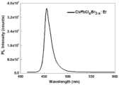
图1a中样品的沉积温度的对应区间为:大于等于530℃且小于等于580℃;图1a中样品1秒时采集的光谱发射峰为452nm,激光照射至发光光谱稳定,10分钟时采集光谱发射峰为455nm、515nm;The corresponding interval of the deposition temperature of the sample in Figure 1a is: greater than or equal to 530°C and less than or equal to 580°C; the spectral emission peak of the sample in Figure 1a collected at 1 second is 452nm, the laser is irradiated until the emission spectrum is stable, and the spectral emission is collected at 10 minutes The peaks are 455nm and 515nm;
图1b中样品的沉积温度的对应区间为:大于等于580℃且小于等于630℃;图1b中样品1秒时采集的光谱发射峰为480nm,激光照射至发光光谱稳定,10分钟时采集光谱发射峰为455nm、510nm、680nm;The corresponding interval of the deposition temperature of the sample in Figure 1b is: greater than or equal to 580°C and less than or equal to 630°C; the spectral emission peak of the sample in Figure 1b collected at 1 second is 480nm, the laser is irradiated until the emission spectrum is stable, and the spectral emission is collected at 10 minutes The peaks are 455nm, 510nm, 680nm;
图1c中样品的沉积温度的对应区间为:大于等于630℃且小于等于670℃;图1c中样品在激光照射下发光光谱稳定,采集光谱的发射峰为475nm、800nm。The corresponding interval of the deposition temperature of the sample in Figure 1c is: greater than or equal to 630°C and less than or equal to 670°C; the emission spectrum of the sample in Figure 1c is stable under laser irradiation, and the emission peaks of the collected spectrum are 475nm and 800nm.
由图2可知,图2a中样品尺寸约为12μm*12μm,图2b中样品尺寸约为22μm*20μm,图2c中样品尺寸约为12μm*12μm。其中图2a中样品的沉积温度区间为530~580℃;图2b中样品的沉积温度区间为600~630℃;图2c中样品的沉积温度区间为640~670℃。It can be seen from Figure 2 that the sample size in Figure 2a is about 12 μm*12 μm, the sample size in Figure 2b is about 22 μm*20 μm, and the sample size in Figure 2c is about 12 μm*12 μm. The deposition temperature range of the sample in Figure 2a is 530-580°C; the deposition temperature range of the sample in Figure 2b is 600-630°C; the deposition temperature range of the sample in Figure 2c is 640-670°C.
对比例1:Comparative example 1:
其他条件与实施例1一致,不同之处在于:Other conditions are consistent with embodiment 1, the difference is:
将高温区在25分钟内从室温升到设定温度;此时,无水氯化铒粉末的受热温度约为820℃,并保持10分钟(此时SiO2/Si晶片衬底样品沉积温度为490~630℃、溴化铯与氯化铅混合粉末的受热温度约为700℃),加热过程完成后,待管式炉降至室温,取出样品。图3是对比例1利用化学气相沉积方法制备的高质量的Er3+掺杂全无机钙钛矿微米片的发光光谱图,从光谱图中可以看出可见光波段仅存在一个发射峰,该发射峰为无相分离时钙钛矿微米片的本征发射峰,位于455nm。因为氯化铒熔点为774℃,加热温度为780℃,铒元素并未掺杂进去钙钛矿晶体中。The high temperature zone was raised from room temperature to the set temperature within 25 minutes; at this time, the heated temperature of the anhydrous erbium chloride powder was about 820°C, and kept for 10 minutes (at this time SiO2 /Si wafer substrate sample deposition temperature 490-630°C, the heating temperature of cesium bromide and lead chloride mixed powder is about 700°C), after the heating process is completed, wait for the tube furnace to cool down to room temperature, and take out the sample. Fig. 3 is the luminescence spectrogram of the high-quality Er3+ doped all-inorganic perovskite microsheet prepared by the chemical vapor deposition method in Comparative Example 1. It can be seen from the spectrogram that there is only one emission peak in the visible light band, and the emission The peak is the intrinsic emission peak of the perovskite microsheets when there is no phase separation, and it is located at 455nm. Because the melting point of erbium chloride is 774°C and the heating temperature is 780°C, the erbium element is not doped into the perovskite crystal.
对比例2:Comparative example 2:
其他条件与实施例1一致,不同之处在于:Other conditions are consistent with embodiment 1, the difference is:
SiO2/Si晶片衬底(1cm×1.5cm)放置于石英管下游的低温区域,当生长温度高于670℃时(SiO2/Si晶片的受热温度的最低温约为675℃,温度分布约为675-690℃,取样部分的温度约为680℃),光谱无双峰发射峰;样品形貌如图4,无规整形貌,无微米片状样品。SiO2 /Si wafer substrate (1cm×1.5cm)is placed in the low temperature area downstream of the quartz tube. 675-690 °C, the temperature of the sampling part is about 680 °C), the spectrum has no double-peak emission peaks; the sample morphology is shown in Figure 4, with random shapes and no micron flake samples.
对比例3:Comparative example 3:
其他条件与实施例1一致,不同之处在于:Other conditions are consistent with embodiment 1, the difference is:
SiO2/Si晶片衬底(1cm×1.5cm)放置于石英管下游的低温区域,生长温度低于520℃时(SiO2/Si晶片的受热温度的最高温约为520,温度分布约为485-520℃取样部分的温度约为510℃),光谱上无相分离的双峰发射峰;样品形貌如图5,绝大部分样品呈半球形,且形貌不规整。SiO2 /Si wafer substrate (1cm×1.5cm) is placed in the low temperature area downstream of the quartz tube, when the growth temperature is lower than 520°C (the maximum temperature of the SiO2 /Si wafer is about 520°C, and the temperature distribution is about 485°C The temperature of the sampling part at -520°C is about 510°C), and there is no phase-separated double-peak emission peak in the spectrum; the sample morphology is shown in Figure 5, most of the samples are hemispherical, and the shape is irregular.
对比例4:Comparative example 4:
1)将氯化铒与摩尔比0.1mol:0.1mol混合的溴化铯和氯化铅粉末分别放入两个磁舟中,然后将磁舟推入直径为25mm,长为80cm的两端封闭的管式炉内的石英管高温区内,溴化铯与氯化铅混合粉末置于石英管内靠近管式炉进气端边缘内的磁舟中,无水氯化铒粉末置于管式炉中央的磁舟中;1) Put erbium chloride and cesium bromide and lead chloride powder mixed with a molar ratio of 0.1mol:0.1mol into two magnetic boats respectively, and then push the magnetic boats into the two ends with a diameter of 25mm and a length of 80cm to seal In the high-temperature zone of the quartz tube in the tube furnace, the mixed powder of cesium bromide and lead chloride is placed in the magnetic boat in the quartz tube near the edge of the inlet end of the tube furnace, and the anhydrous erbium chloride powder is placed in the tube furnace In the central magnetic boat;
2)将SiO2/Si晶片衬底(1cm×1.5cm)放置在磁舟上,然后将磁舟置于石英管下游的低温区域;2) Place the SiO2 /Si wafer substrate (1cm×1.5cm) on the magnetic boat, and then place the magnetic boat in the low temperature area downstream of the quartz tube;
3)将管式炉密封后,通入流速为1000sccm以上的高纯惰性气体5分钟进行洗气,然后将高纯惰性气体流速调节至40sccm,并开启升温程序。3) After sealing the tube furnace, inject a high-purity inert gas with a flow rate of 1000 sccm or more for 5 minutes for scrubbing, then adjust the flow rate of the high-purity inert gas to 40 sccm, and start the heating program.
4)将高温区在25分钟内从室温升到设定温度,此时溴化铯与氯化铅混合粉末的受热温度约为785℃,无水氯化铒粉末的受热温度约为832℃,并保持10分钟(此时SiO2/Si晶片衬底样品沉积温度为530~670℃),加热过程完成后,待管式炉降至室温,取出样品。4) Raise the high temperature zone from room temperature to the set temperature within 25 minutes. At this time, the heating temperature of the cesium bromide and lead chloride mixed powder is about 785°C, and the heating temperature of the anhydrous erbium chloride powder is about 832°C , and kept for 10 minutes (at this time, the SiO2 /Si wafer substrate sample deposition temperature was 530-670° C.), after the heating process was completed, the tube furnace was cooled to room temperature, and the sample was taken out.
图6是对比例4所得样品的光学照片,从图中可以看出有零星形貌较规整的正方形状微米片,但大多数呈现出粒径不一的球形或椭球形,其可能由于载气流速过大,生长的规则形貌微米片少。Figure 6 is an optical photo of the sample obtained in Comparative Example 4. It can be seen from the figure that there are sporadic square microflakes with regular shapes, but most of them present spherical or ellipsoidal shapes with different particle sizes, which may be caused by the carrier gas flow. If the speed is too high, there will be few micro-sheets with regular morphology.
以上所述对本发明创造的实施方案进行了具体的说明,但不是全部或者唯一的方案,在本领域内的普通技术人员在不违背本发明创造精神的情况下对本发明技术方案采用的任何等效的变换,均应包含在本发明的保护范围之内。The above has specifically described the embodiments of the present invention, but not all or the only solutions, any equivalents adopted by those of ordinary skill in the art to the technical solutions of the present invention without violating the spirit of the present invention All changes should be included within the protection scope of the present invention.
Claims (1)
Translated fromChinesePriority Applications (1)
| Application Number | Priority Date | Filing Date | Title |
|---|---|---|---|
| CN202210574231.8ACN114988462B (en) | 2022-05-25 | 2022-05-25 | Method for preparing perovskite micron sheet with multi-wavelength emission based on chemical vapor deposition method |
Applications Claiming Priority (1)
| Application Number | Priority Date | Filing Date | Title |
|---|---|---|---|
| CN202210574231.8ACN114988462B (en) | 2022-05-25 | 2022-05-25 | Method for preparing perovskite micron sheet with multi-wavelength emission based on chemical vapor deposition method |
Publications (2)
| Publication Number | Publication Date |
|---|---|
| CN114988462A CN114988462A (en) | 2022-09-02 |
| CN114988462Btrue CN114988462B (en) | 2023-06-09 |
Family
ID=83029686
Family Applications (1)
| Application Number | Title | Priority Date | Filing Date |
|---|---|---|---|
| CN202210574231.8AActiveCN114988462B (en) | 2022-05-25 | 2022-05-25 | Method for preparing perovskite micron sheet with multi-wavelength emission based on chemical vapor deposition method |
Country Status (1)
| Country | Link |
|---|---|
| CN (1) | CN114988462B (en) |
Families Citing this family (1)
| Publication number | Priority date | Publication date | Assignee | Title |
|---|---|---|---|---|
| CN115710693B (en)* | 2022-09-21 | 2024-12-24 | 西安奕斯伟材料科技股份有限公司 | Dopant and preparation method thereof, doped silicon wafer and manufacturing method thereof |
Family Cites Families (4)
| Publication number | Priority date | Publication date | Assignee | Title |
|---|---|---|---|---|
| CN108075020B (en)* | 2017-12-27 | 2020-10-16 | 中国科学院长春光学精密机械与物理研究所 | Light-emitting diode based on cesium-lead halogen perovskite thin film material and preparation method thereof |
| CN110571136B (en)* | 2019-09-09 | 2022-05-03 | 陕西科技大学 | Preparation method of lead-free all-inorganic perovskite film by one-step chemical vapor deposition |
| CN110911506A (en)* | 2019-11-28 | 2020-03-24 | 南京大学 | Rare earth Er doped highly stable all-inorganic perovskite solar cell and preparation method |
| CN113025327B (en)* | 2021-03-25 | 2022-06-21 | 昆明理工大学 | Multi-mode luminous lead-free double perovskite material and preparation method thereof |
- 2022
- 2022-05-25CNCN202210574231.8Apatent/CN114988462B/enactiveActive
Also Published As
| Publication number | Publication date |
|---|---|
| CN114988462A (en) | 2022-09-02 |
Similar Documents
| Publication | Publication Date | Title |
|---|---|---|
| Wang et al. | Original core–shell structure of cubic CsPbBr3@ amorphous CsPbBr x perovskite quantum dots with a high blue photoluminescence quantum yield of over 80% | |
| Yuan et al. | In situ crystallization synthesis of CsPbBr3 perovskite quantum dot-embedded glasses with improved stability for solid-state lighting and random upconverted lasing | |
| CN106833635B (en) | Preparation method of large size perovskite CsPbBr3 hexagonal sheet-circular sheet | |
| CN110938428B (en) | A method for efficient synthesis of Cs2AgCl3 all-inorganic non-lead perovskite | |
| CN110684529B (en) | Subminiature perovskite quantum dot and preparation method thereof | |
| Kumar et al. | Luminescence properties of rare-earth doped oxide materials | |
| CN114988462B (en) | Method for preparing perovskite micron sheet with multi-wavelength emission based on chemical vapor deposition method | |
| Wu et al. | In situ fabricated perovskite quantum dots: from materials to applications | |
| Ma et al. | Atomic layer deposition and electroluminescence of Er-doped polycrystalline Lu3Ga5O12 nanofilms for silicon-based optoelectronics | |
| CN114315646B (en) | Preparation method of small-size blue-light perovskite nanocrystalline | |
| Zhang et al. | Photovoltaic efficiency enhancement for crystalline silicon solar cells via a Bi-functional layer based on europium complex@ nanozeolite@ SiO2 | |
| CN110790299B (en) | A simple method for the synthesis of CsAg2I3 pure-phase inorganic non-lead perovskites | |
| CN103014864B (en) | A kind of mid-infrared luminescent crystal material, and preparation method and application | |
| CN109880624B (en) | Preparation method of ultra-small PbSe quantum dots | |
| Tang et al. | Effect of perovskite composition regulation on its crystallization in SiO2–Al2O3–Li2CO3–AlF3–LiF glass system | |
| CN103011236B (en) | A kind of holmium metal iodate fluorescent material and its preparation method and application | |
| Hassan et al. | Synthesis and photoluminescent properties of Sr (1− x) Si2O2N2: xEu2+ phosphor prepared by polymer metal complex method for WLEDs applications | |
| CN105970293B (en) | It is a kind of using four gadolinium molydbate barium as the laser material and its preparation method and application of host doped Rare earth element ytterbium neodymium | |
| CN106012016B (en) | A kind of adjustable up-conversion luminescence non-plumbum ferroelectric monocrystal of electricity and preparation method thereof | |
| Wang et al. | Synthesis of Colloidal Perovskite CH3NH3PbBr3-xClx Nanocrystals with Lead Acetate | |
| CN109824024B (en) | A kind of preparation method of lanthanide doped zinc selenide nanomaterial | |
| Xu et al. | Single-Crystal Terbium Silicate Chloride Core–Shell Nanowires and Nanotubes for Monolithically Integrated Optoelectronics | |
| Marcondes et al. | CdTe QD/Er3+-doped SiO2–Nb2O5 nanocomposites: Thermal, structural and photophysical properties | |
| CN106835280B (en) | A kind of rare earth ion Ln3+Doping gadolinium aluminate strontium laser crystal | |
| Zhang et al. | Effect of melting times on the down-shifting properties in Ce3+-doped oxyfluoride glass ceramics for a-Si solar cells |
Legal Events
| Date | Code | Title | Description |
|---|---|---|---|
| PB01 | Publication | ||
| PB01 | Publication | ||
| SE01 | Entry into force of request for substantive examination | ||
| SE01 | Entry into force of request for substantive examination | ||
| GR01 | Patent grant | ||
| GR01 | Patent grant |