CN114981472A - Selective deposition of passive films on metal surfaces - Google Patents
Selective deposition of passive films on metal surfacesDownload PDFInfo
- Publication number
- CN114981472A CN114981472ACN202180003878.9ACN202180003878ACN114981472ACN 114981472 ACN114981472 ACN 114981472ACN 202180003878 ACN202180003878 ACN 202180003878ACN 114981472 ACN114981472 ACN 114981472A
- Authority
- CN
- China
- Prior art keywords
- docking
- precursor
- substrate
- group
- metal surface
- Prior art date
- Legal status (The legal status is an assumption and is not a legal conclusion. Google has not performed a legal analysis and makes no representation as to the accuracy of the status listed.)
- Granted
Links
Images


Classifications
- H—ELECTRICITY
- H01—ELECTRIC ELEMENTS
- H01L—SEMICONDUCTOR DEVICES NOT COVERED BY CLASS H10
- H01L21/00—Processes or apparatus adapted for the manufacture or treatment of semiconductor or solid state devices or of parts thereof
- H01L21/02—Manufacture or treatment of semiconductor devices or of parts thereof
- H01L21/02104—Forming layers
- H01L21/02107—Forming insulating materials on a substrate
- H01L21/02109—Forming insulating materials on a substrate characterised by the type of layer, e.g. type of material, porous/non-porous, pre-cursors, mixtures or laminates
- H01L21/02205—Forming insulating materials on a substrate characterised by the type of layer, e.g. type of material, porous/non-porous, pre-cursors, mixtures or laminates the layer being characterised by the precursor material for deposition
- C—CHEMISTRY; METALLURGY
- C23—COATING METALLIC MATERIAL; COATING MATERIAL WITH METALLIC MATERIAL; CHEMICAL SURFACE TREATMENT; DIFFUSION TREATMENT OF METALLIC MATERIAL; COATING BY VACUUM EVAPORATION, BY SPUTTERING, BY ION IMPLANTATION OR BY CHEMICAL VAPOUR DEPOSITION, IN GENERAL; INHIBITING CORROSION OF METALLIC MATERIAL OR INCRUSTATION IN GENERAL
- C23C—COATING METALLIC MATERIAL; COATING MATERIAL WITH METALLIC MATERIAL; SURFACE TREATMENT OF METALLIC MATERIAL BY DIFFUSION INTO THE SURFACE, BY CHEMICAL CONVERSION OR SUBSTITUTION; COATING BY VACUUM EVAPORATION, BY SPUTTERING, BY ION IMPLANTATION OR BY CHEMICAL VAPOUR DEPOSITION, IN GENERAL
- C23C16/00—Chemical coating by decomposition of gaseous compounds, without leaving reaction products of surface material in the coating, i.e. chemical vapour deposition [CVD] processes
- C23C16/44—Chemical coating by decomposition of gaseous compounds, without leaving reaction products of surface material in the coating, i.e. chemical vapour deposition [CVD] processes characterised by the method of coating
- C23C16/455—Chemical coating by decomposition of gaseous compounds, without leaving reaction products of surface material in the coating, i.e. chemical vapour deposition [CVD] processes characterised by the method of coating characterised by the method used for introducing gases into reaction chamber or for modifying gas flows in reaction chamber
- C23C16/45523—Pulsed gas flow or change of composition over time
- C23C16/45525—Atomic layer deposition [ALD]
- C23C16/45553—Atomic layer deposition [ALD] characterized by the use of precursors specially adapted for ALD
- C—CHEMISTRY; METALLURGY
- C23—COATING METALLIC MATERIAL; COATING MATERIAL WITH METALLIC MATERIAL; CHEMICAL SURFACE TREATMENT; DIFFUSION TREATMENT OF METALLIC MATERIAL; COATING BY VACUUM EVAPORATION, BY SPUTTERING, BY ION IMPLANTATION OR BY CHEMICAL VAPOUR DEPOSITION, IN GENERAL; INHIBITING CORROSION OF METALLIC MATERIAL OR INCRUSTATION IN GENERAL
- C23C—COATING METALLIC MATERIAL; COATING MATERIAL WITH METALLIC MATERIAL; SURFACE TREATMENT OF METALLIC MATERIAL BY DIFFUSION INTO THE SURFACE, BY CHEMICAL CONVERSION OR SUBSTITUTION; COATING BY VACUUM EVAPORATION, BY SPUTTERING, BY ION IMPLANTATION OR BY CHEMICAL VAPOUR DEPOSITION, IN GENERAL
- C23C16/00—Chemical coating by decomposition of gaseous compounds, without leaving reaction products of surface material in the coating, i.e. chemical vapour deposition [CVD] processes
- C23C16/04—Coating on selected surface areas, e.g. using masks
- C—CHEMISTRY; METALLURGY
- C23—COATING METALLIC MATERIAL; COATING MATERIAL WITH METALLIC MATERIAL; CHEMICAL SURFACE TREATMENT; DIFFUSION TREATMENT OF METALLIC MATERIAL; COATING BY VACUUM EVAPORATION, BY SPUTTERING, BY ION IMPLANTATION OR BY CHEMICAL VAPOUR DEPOSITION, IN GENERAL; INHIBITING CORROSION OF METALLIC MATERIAL OR INCRUSTATION IN GENERAL
- C23C—COATING METALLIC MATERIAL; COATING MATERIAL WITH METALLIC MATERIAL; SURFACE TREATMENT OF METALLIC MATERIAL BY DIFFUSION INTO THE SURFACE, BY CHEMICAL CONVERSION OR SUBSTITUTION; COATING BY VACUUM EVAPORATION, BY SPUTTERING, BY ION IMPLANTATION OR BY CHEMICAL VAPOUR DEPOSITION, IN GENERAL
- C23C16/00—Chemical coating by decomposition of gaseous compounds, without leaving reaction products of surface material in the coating, i.e. chemical vapour deposition [CVD] processes
- C23C16/44—Chemical coating by decomposition of gaseous compounds, without leaving reaction products of surface material in the coating, i.e. chemical vapour deposition [CVD] processes characterised by the method of coating
- C23C16/455—Chemical coating by decomposition of gaseous compounds, without leaving reaction products of surface material in the coating, i.e. chemical vapour deposition [CVD] processes characterised by the method of coating characterised by the method used for introducing gases into reaction chamber or for modifying gas flows in reaction chamber
- C23C16/45523—Pulsed gas flow or change of composition over time
- C23C16/45525—Atomic layer deposition [ALD]
- C23C16/45527—Atomic layer deposition [ALD] characterized by the ALD cycle, e.g. different flows or temperatures during half-reactions, unusual pulsing sequence, use of precursor mixtures or auxiliary reactants or activations
- C23C16/45534—Use of auxiliary reactants other than used for contributing to the composition of the main film, e.g. catalysts, activators or scavengers
- H—ELECTRICITY
- H01—ELECTRIC ELEMENTS
- H01L—SEMICONDUCTOR DEVICES NOT COVERED BY CLASS H10
- H01L21/00—Processes or apparatus adapted for the manufacture or treatment of semiconductor or solid state devices or of parts thereof
- H01L21/02—Manufacture or treatment of semiconductor devices or of parts thereof
- H01L21/02104—Forming layers
- H01L21/02107—Forming insulating materials on a substrate
- H01L21/02109—Forming insulating materials on a substrate characterised by the type of layer, e.g. type of material, porous/non-porous, pre-cursors, mixtures or laminates
- H01L21/02112—Forming insulating materials on a substrate characterised by the type of layer, e.g. type of material, porous/non-porous, pre-cursors, mixtures or laminates characterised by the material of the layer
- H01L21/02118—Forming insulating materials on a substrate characterised by the type of layer, e.g. type of material, porous/non-porous, pre-cursors, mixtures or laminates characterised by the material of the layer carbon based polymeric organic or inorganic material, e.g. polyimides, poly cyclobutene or PVC
- H—ELECTRICITY
- H01—ELECTRIC ELEMENTS
- H01L—SEMICONDUCTOR DEVICES NOT COVERED BY CLASS H10
- H01L21/00—Processes or apparatus adapted for the manufacture or treatment of semiconductor or solid state devices or of parts thereof
- H01L21/02—Manufacture or treatment of semiconductor devices or of parts thereof
- H01L21/02104—Forming layers
- H01L21/02107—Forming insulating materials on a substrate
- H01L21/02109—Forming insulating materials on a substrate characterised by the type of layer, e.g. type of material, porous/non-porous, pre-cursors, mixtures or laminates
- H01L21/02112—Forming insulating materials on a substrate characterised by the type of layer, e.g. type of material, porous/non-porous, pre-cursors, mixtures or laminates characterised by the material of the layer
- H01L21/02123—Forming insulating materials on a substrate characterised by the type of layer, e.g. type of material, porous/non-porous, pre-cursors, mixtures or laminates characterised by the material of the layer the material containing silicon
- H01L21/02164—Forming insulating materials on a substrate characterised by the type of layer, e.g. type of material, porous/non-porous, pre-cursors, mixtures or laminates characterised by the material of the layer the material containing silicon the material being a silicon oxide, e.g. SiO2
- H—ELECTRICITY
- H01—ELECTRIC ELEMENTS
- H01L—SEMICONDUCTOR DEVICES NOT COVERED BY CLASS H10
- H01L21/00—Processes or apparatus adapted for the manufacture or treatment of semiconductor or solid state devices or of parts thereof
- H01L21/02—Manufacture or treatment of semiconductor devices or of parts thereof
- H01L21/02104—Forming layers
- H01L21/02107—Forming insulating materials on a substrate
- H01L21/02225—Forming insulating materials on a substrate characterised by the process for the formation of the insulating layer
- H01L21/0226—Forming insulating materials on a substrate characterised by the process for the formation of the insulating layer formation by a deposition process
- H01L21/02263—Forming insulating materials on a substrate characterised by the process for the formation of the insulating layer formation by a deposition process deposition from the gas or vapour phase
- H01L21/02271—Forming insulating materials on a substrate characterised by the process for the formation of the insulating layer formation by a deposition process deposition from the gas or vapour phase deposition by decomposition or reaction of gaseous or vapour phase compounds, i.e. chemical vapour deposition
- H—ELECTRICITY
- H01—ELECTRIC ELEMENTS
- H01L—SEMICONDUCTOR DEVICES NOT COVERED BY CLASS H10
- H01L21/00—Processes or apparatus adapted for the manufacture or treatment of semiconductor or solid state devices or of parts thereof
- H01L21/02—Manufacture or treatment of semiconductor devices or of parts thereof
- H01L21/02104—Forming layers
- H01L21/02107—Forming insulating materials on a substrate
- H01L21/02296—Forming insulating materials on a substrate characterised by the treatment performed before or after the formation of the layer
- H01L21/02299—Forming insulating materials on a substrate characterised by the treatment performed before or after the formation of the layer pre-treatment
- H—ELECTRICITY
- H01—ELECTRIC ELEMENTS
- H01L—SEMICONDUCTOR DEVICES NOT COVERED BY CLASS H10
- H01L21/00—Processes or apparatus adapted for the manufacture or treatment of semiconductor or solid state devices or of parts thereof
- H01L21/02—Manufacture or treatment of semiconductor devices or of parts thereof
- H01L21/04—Manufacture or treatment of semiconductor devices or of parts thereof the devices having potential barriers, e.g. a PN junction, depletion layer or carrier concentration layer
- H01L21/18—Manufacture or treatment of semiconductor devices or of parts thereof the devices having potential barriers, e.g. a PN junction, depletion layer or carrier concentration layer the devices having semiconductor bodies comprising elements of Group IV of the Periodic Table or AIIIBV compounds with or without impurities, e.g. doping materials
- H01L21/30—Treatment of semiconductor bodies using processes or apparatus not provided for in groups H01L21/20 - H01L21/26
- H01L21/31—Treatment of semiconductor bodies using processes or apparatus not provided for in groups H01L21/20 - H01L21/26 to form insulating layers thereon, e.g. for masking or by using photolithographic techniques; After treatment of these layers; Selection of materials for these layers
- H01L21/32—Treatment of semiconductor bodies using processes or apparatus not provided for in groups H01L21/20 - H01L21/26 to form insulating layers thereon, e.g. for masking or by using photolithographic techniques; After treatment of these layers; Selection of materials for these layers using masks
- B—PERFORMING OPERATIONS; TRANSPORTING
- B05—SPRAYING OR ATOMISING IN GENERAL; APPLYING FLUENT MATERIALS TO SURFACES, IN GENERAL
- B05D—PROCESSES FOR APPLYING FLUENT MATERIALS TO SURFACES, IN GENERAL
- B05D1/00—Processes for applying liquids or other fluent materials
- B05D1/32—Processes for applying liquids or other fluent materials using means for protecting parts of a surface not to be coated, e.g. using stencils, resists
- B—PERFORMING OPERATIONS; TRANSPORTING
- B05—SPRAYING OR ATOMISING IN GENERAL; APPLYING FLUENT MATERIALS TO SURFACES, IN GENERAL
- B05D—PROCESSES FOR APPLYING FLUENT MATERIALS TO SURFACES, IN GENERAL
- B05D1/00—Processes for applying liquids or other fluent materials
- B05D1/60—Deposition of organic layers from vapour phase
- H—ELECTRICITY
- H01—ELECTRIC ELEMENTS
- H01L—SEMICONDUCTOR DEVICES NOT COVERED BY CLASS H10
- H01L21/00—Processes or apparatus adapted for the manufacture or treatment of semiconductor or solid state devices or of parts thereof
- H01L21/02—Manufacture or treatment of semiconductor devices or of parts thereof
- H01L21/02104—Forming layers
- H01L21/02107—Forming insulating materials on a substrate
- H01L21/02225—Forming insulating materials on a substrate characterised by the process for the formation of the insulating layer
- H01L21/0226—Forming insulating materials on a substrate characterised by the process for the formation of the insulating layer formation by a deposition process
- H01L21/02263—Forming insulating materials on a substrate characterised by the process for the formation of the insulating layer formation by a deposition process deposition from the gas or vapour phase
- H01L21/02271—Forming insulating materials on a substrate characterised by the process for the formation of the insulating layer formation by a deposition process deposition from the gas or vapour phase deposition by decomposition or reaction of gaseous or vapour phase compounds, i.e. chemical vapour deposition
- H01L21/0228—Forming insulating materials on a substrate characterised by the process for the formation of the insulating layer formation by a deposition process deposition from the gas or vapour phase deposition by decomposition or reaction of gaseous or vapour phase compounds, i.e. chemical vapour deposition deposition by cyclic CVD, e.g. ALD, ALE, pulsed CVD
Landscapes
- Chemical & Material Sciences (AREA)
- Engineering & Computer Science (AREA)
- Manufacturing & Machinery (AREA)
- Chemical Kinetics & Catalysis (AREA)
- Physics & Mathematics (AREA)
- Computer Hardware Design (AREA)
- Microelectronics & Electronic Packaging (AREA)
- Power Engineering (AREA)
- Condensed Matter Physics & Semiconductors (AREA)
- General Physics & Mathematics (AREA)
- General Chemical & Material Sciences (AREA)
- Materials Engineering (AREA)
- Mechanical Engineering (AREA)
- Metallurgy (AREA)
- Organic Chemistry (AREA)
- Chemical Vapour Deposition (AREA)
- Formation Of Insulating Films (AREA)
Abstract
Translated fromChinese
Description
Translated fromChinese技术领域technical field
本公开内容的多个实施方式涉及用于选择性沉积钝化膜的方法。特别地,本公开内容的多个实施方式针对在金属表面上选择性地沉积钝化膜的方法。Various embodiments of the present disclosure relate to methods for selectively depositing passivation films. In particular, various embodiments of the present disclosure are directed to methods of selectively depositing passivation films on metal surfaces.
背景技术Background technique
半导体行业在追求涉及纳米级特征快速缩放的装置小型化方面面临许多挑战。这些问题包括复杂的制造步骤(诸如多个平板印刷步骤和高性能材料的集成)的引入。为了保持装置小型化的节奏,选择性沉积已显示出有效前景,因为它有可能通过简化集成方案来消除高成本的平板印刷步骤。The semiconductor industry faces many challenges in the pursuit of device miniaturization involving rapid scaling of nanoscale features. These problems include the introduction of complex manufacturing steps such as multiple lithography steps and the integration of high performance materials. To maintain the pace of device miniaturization, selective deposition has shown promising promise as it has the potential to eliminate costly lithography steps by simplifying the integration scheme.
材料的选择性沉积能以多种方式实现。相对于一个表面(金属或电介质),化学前驱物可以选择性地与另一个表面反应。可调节诸如压强、基板温度、前驱物分压和/或气流之类的工艺参数以调节特定表面反应的化学动力学。另一种可能的方案涉及表面预处理,所述预处理能用于激活或钝化对进入的薄膜沉积前驱物感兴趣的表面。Selective deposition of materials can be accomplished in a number of ways. With respect to one surface (metal or dielectric), chemical precursors can selectively react with another surface. Process parameters such as pressure, substrate temperature, precursor partial pressure, and/or gas flow can be adjusted to tune the chemical kinetics of specific surface reactions. Another possible solution involves surface pretreatment, which can be used to activate or passivate surfaces of interest for incoming thin film deposition precursors.
诸如AS-ALD的自下而上的方法已越来越多地用于实现具有纳米控制的图案化架构。在本领域中持续需要用于提高沉积选择性的方法。由于输送的低蒸气压强,蒸气自组装单层(self-assembled monolayer;SAM)沉积的使用在使用具有较长链的SAM配位体时具有限制。另一方面,如果长链不是使用湿SAM沉积的垂直对准,则具有长链的配位体可能无效。提供改进的AS-ALD工艺将是有益的。Bottom-up approaches such as AS-ALD have been increasingly used to achieve patterned architectures with nanoscale control. There is a continuing need in the art for methods for improving deposition selectivity. The use of vapor self-assembled monolayer (SAM) deposition has limitations when using SAM ligands with longer chains due to the low vapor pressure delivered. On the other hand, ligands with long chains may be ineffective if the long chains are not vertically aligned using wet SAM deposition. It would be beneficial to provide an improved AS-ALD process.
发明内容SUMMARY OF THE INVENTION
在第一方面中,一种在基板上选择性沉积膜的方法包含:将包括金属表面和介电表面的基板表面暴露于对接前驱物;并且在金属表面选择性地沉积对接前驱物以形成对接层,其中对接前驱物是具有与金属表面选择性反应和结合的头部基团的芳烃。In a first aspect, a method of selectively depositing a film on a substrate comprises: exposing a substrate surface including a metal surface and a dielectric surface to a docking precursor; and selectively depositing the docking precursor on the metal surface to form a docking layer in which the docking precursor is an aromatic hydrocarbon with a head group that selectively reacts and binds to the metal surface.
另一个实施方式关于在基板上选择性沉积膜的方法,所述方法包含将包括金属表面和介电表面的基板表面暴露于对接前驱物;选择性地在金属表面沉积对接前驱物以形成对接层,其中所述对接前驱物是具有头部基团的芳烃,其中芳烃是杂环芳族化合物,所述杂环芳族化合物选自由吡咯、噻吩、苯胺,和3,4-乙烯二氧噻吩(ethylenedioxythiophene,EDOT)组成的群组;在催化剂存在下,将对接层的对接前驱物与链单体聚合一次或多次以沉积钝化膜。Another embodiment pertains to a method of selectively depositing a film on a substrate, the method comprising exposing a substrate surface comprising a metal surface and a dielectric surface to a docking precursor; selectively depositing the docking precursor on the metal surface to form a docking layer , wherein the docking precursor is an aromatic hydrocarbon with a head group, wherein the aromatic hydrocarbon is a heterocyclic aromatic compound selected from pyrrole, thiophene, aniline, and 3,4-ethylenedioxythiophene ( ethylenedioxythiophene, EDOT); in the presence of a catalyst, the docking precursor of the docking layer and the chain monomer are polymerized one or more times to deposit a passivation film.
另一方面关于一种包括指令的非暂时性计算机可读介质,所述指令在由基板处理腔室的控制器执行时使基板处理腔室将包括金属表面和介电表面的基板表面暴露于对接前驱物;并且选择性地将对接前驱物沉积在金属表面上以形成对接层,其中对接前驱物是具有选择性地与金属表面反应和结合的头部基团的芳烃。Another aspect relates to a non-transitory computer readable medium comprising instructions that, when executed by a controller of a substrate processing chamber, cause the substrate processing chamber to expose a substrate surface, including a metal surface and a dielectric surface, to a docking and selectively depositing a docking precursor on the metal surface to form a docking layer, wherein the docking precursor is an aromatic hydrocarbon having a head group that selectively reacts and binds to the metal surface.
附图说明Description of drawings
为了能详细理解本公开内容的上述特征的方式,可参考多个实施方式获得上文简要概述的本公开内容的更具体描述,所述多个实施方式中的一些实施方式在附图中示出。然而,应注意,附图仅示出本公开内容的多个典型实施方式并且因此不视为本公开内容范围的限制,因为本公开内容可允许其他多个同等有效的实施方式。In order that the manner in which the above-described features of the present disclosure can be understood in detail, a more detailed description of the present disclosure, briefly summarized above, may be obtained by reference to a number of embodiments, some of which are illustrated in the accompanying drawings. . It is to be noted, however, that the appended drawings illustrate only several typical embodiments of this disclosure and are therefore not to be considered limiting of its scope, for the present disclosure may admit to many other equally effective embodiments.
图1示出根据本公开内容的实施方式的用于在基板表面上选择性沉积钝化膜的方法的反应示意图;FIG. 1 shows a reaction schematic diagram of a method for selectively depositing a passivation film on a substrate surface according to an embodiment of the present disclosure;
图2示出根据本公开内容的实施方式的用于在基板表面上选择性沉积钝化膜的方法的反应示意图;和FIG. 2 shows a reaction schematic diagram of a method for selectively depositing a passivation film on a substrate surface according to an embodiment of the present disclosure; and
图3是根据本公开内容的实施方式的方法的流程图。3 is a flowchart of a method according to an embodiment of the present disclosure.
具体实施方式Detailed ways
在描述本发明的若干示例性实施方式之前,应当理解,本发明不限于在以下描述中阐述的结构或工艺步骤的细节。本发明能够具有其他多个实施方式并且能够以各种方式被实践或执行。Before several exemplary embodiments of the invention are described, it is to be understood that the invention is not limited to the details of structure or process steps set forth in the following description. The invention is capable of other various embodiments and of being practiced or carried out in various ways.
如本文中所使用的“基板”或“基板表面”是指基板的任何部分或者在基板上形成的材料表面的一部分,在基板的任何部分或者在基板上形成的材料表面的一部分上进行膜处理。例如,取决于应用,在能在基板表面上进行处理的基板表面包括诸如硅、氧化硅、氮化硅、掺杂硅、锗、砷化镓、玻璃、蓝宝石的材料,和诸如金属、金属氮化物、金属合金的任何其他材料,和其他导电材料。基板包括但不限于半导体晶片。基板可暴露于预处理工艺以抛光、蚀刻、清洁、还原、氧化、羟基化、退火、紫外线固化、电子束固化和/或烘烤基板表面。除了直接在基板本身的表面上进行的膜处理之外,在本公开内容中,所公开的任何膜处理步骤也可以在如下文更详细公开的基板上形成的底层上进行,并且术语“基板表面”旨在包括如上下文所示的底层。因此,例如,当膜/层或部分膜/层已经沉积到基板表面上时,新沉积的膜/层的暴露表面成为基板表面。基板可具有各种尺寸,例如直径是200mm或300mm的晶片,以及矩形或方形方格。在一些实施方式中,基板包含刚性非连续材料。"Substrate" or "substrate surface" as used herein refers to any portion of the substrate or portion of the surface of the material formed on the substrate on which the film treatment is performed . For example, depending on the application, substrate surfaces that can be processed on the substrate surface include materials such as silicon, silicon oxide, silicon nitride, doped silicon, germanium, gallium arsenide, glass, sapphire, and materials such as metals, metal nitrides Any other material of metal alloys, metal alloys, and other conductive materials. Substrates include, but are not limited to, semiconductor wafers. The substrate may be exposed to a pretreatment process to polish, etch, clean, reduce, oxidize, hydroxylate, anneal, UV cure, e-beam cure, and/or bake the surface of the substrate. In addition to film processing performed directly on the surface of the substrate itself, in this disclosure, any of the film processing steps disclosed may also be performed on an underlying layer formed on the substrate as disclosed in more detail below, and the term "substrate surface " is intended to include the underlying layers as the context indicates. Thus, for example, when a film/layer or part of a film/layer has already been deposited on the substrate surface, the exposed surface of the newly deposited film/layer becomes the substrate surface. The substrates can be of various sizes, such as wafers with diameters of 200mm or 300mm, and rectangular or square grids. In some embodiments, the substrate comprises a rigid discontinuous material.
如本文使用的“原子层沉积”或“循环沉积”代表连续暴露两种或更多种反应化合物以在基板表面上沉积一个材料层的工艺。"Atomic layer deposition" or "cyclic deposition" as used herein refers to the process of sequentially exposing two or more reactive compounds to deposit a layer of material on the surface of a substrate.
如本说明书和附加权利要求书中所使用,术语“反应化合物”、“反应气体”、“反应物种(species)”、“前驱物”、“工艺气体”和类似术语可互换使用以意指具有一物种的物质(substance),所述物种能够在表面反应(例如,化学吸附、氧化、还原、环加成)中与基板表面或基板表面上的材料反应。基板或基板的一部分依次暴露于被引入处理腔室的反应区域的两种或更多种反应化合物。As used in this specification and the appended claims, the terms "reactive compound," "reactive gas," "reactive species," "precursor," "process gas," and similar terms are used interchangeably to mean A substance having a species capable of reacting with a substrate surface or a material on the substrate surface in a surface reaction (eg, chemisorption, oxidation, reduction, cycloaddition). The substrate or a portion of the substrate is sequentially exposed to two or more reactive compounds introduced into the reaction zone of the processing chamber.
如本文所用,“金属”是指金属、金属合金、金属氧化物、金属氮化物或上述材料的组合,例如包含铜、钴、镍、钨、钒、钌、铬、铁、铂、金、银、钼、镓、铟、氧化铟锡、掺氟氧化锡和掺铝氧化锌。在一个或多个实施方式中,金属氧化物不包括介电氧化物。As used herein, "metal" refers to a metal, metal alloy, metal oxide, metal nitride, or a combination of the foregoing, for example including copper, cobalt, nickel, tungsten, vanadium, ruthenium, chromium, iron, platinum, gold, silver , molybdenum, gallium, indium, indium tin oxide, fluorine-doped tin oxide and aluminum-doped zinc oxide. In one or more embodiments, the metal oxides do not include dielectric oxides.
如本文中所使用,“金属表面”是指由金属形成的基板的任何部分或材料表面的部分。金属表面可暴露于预处理工艺以抛光、涂覆、掺杂、蚀刻、还原、氧化、羟基化、退火、紫外线固化、电子束固化和/或烘烤基板表面。除了直接在金属表面本身进行预处理之外,在本公开内容中,所公开的任何金属表面处理也可以在下文更详细公开的底层金属表面上进行,并且术语“金属表面”旨在包括如上下文所示的该底层。因此,例如,在膜/层或部分膜/层已经沉积到金属表面上的情况下,新沉积的膜/层的暴露表面变成金属表面。As used herein, "metal surface" refers to any portion of a substrate or portion of a material surface formed of metal. Metal surfaces may be exposed to pretreatment processes to polish, coat, dope, etch, reduce, oxidize, hydroxylate, anneal, UV cure, e-beam cure, and/or bake the substrate surface. In addition to the pretreatment directly on the metal surface itself, in this disclosure, any of the metal surface treatments disclosed may also be performed on the underlying metal surface as disclosed in more detail below, and the term "metal surface" is intended to include as contextual the bottom layer shown. Thus, for example, where a film/layer or part of a film/layer has already been deposited on a metal surface, the exposed surface of the newly deposited film/layer becomes the metal surface.
如在本说明书和所附权利要求中所使用,短语“选择性覆盖(over)”或类似术语意指主体材料沉积在所述表面上的程度大于在另一表面上的沉积程度。在一些实施方式中,“选择性地”意指主体材料以一个速率在选择性表面上形成,所述速率大于或等于在非选择性表面上的形成速率的约10x、15x、20x、25x、30x、35x、40x、45x或50x。As used in this specification and the appended claims, the phrase "selectively over" or similar terms means that the host material is deposited on the surface to a greater extent than on another surface. In some embodiments, "selectively" means that the host material is formed on a selective surface at a rate that is greater than or equal to about 10x, 15x, 20x, 25x, 30x, 35x, 40x, 45x or 50x.
本公开内容的多个实施方式有利地提供了用于表面预处理的方法,例如金属表面的选择性封闭。对于封闭,基板用对接前驱物进行预处理。对接前驱物选择性地与金属表面反应和结合,形成对接层。对接层进一步与链单体发生一次或多次聚合反应以形成钝化层。所述方法允许在介电表面上而不是在金属表面上的介电膜的选择性沉积。Various embodiments of the present disclosure advantageously provide methods for surface pretreatment, such as selective sealing of metal surfaces. For sealing, the substrates were pretreated with docking precursors. The docking precursor selectively reacts and combines with the metal surface to form a docking layer. The docking layer further undergoes one or more polymerization reactions with chain monomers to form a passivation layer. The method allows for the selective deposition of dielectric films on dielectric surfaces rather than metal surfaces.
多个实施方式通过在期望的ALD膜旁边逐渐生长聚合物层以减少侧向生长(蘑菇状生长(mushroom))问题来增强自组装单层(SAM)钝化。这样能有助于提高目标表面上的膜选择性。通过选择能使用原子层沉积(ALD)工具与所需的ALD工艺一起沉积的合适的构建块(building block),提供了用于聚合物钝化层的方法。逐渐添加分子前驱物以选择性地结合到金属表面(例如,Cu、Co等),但不在介电(例如,SiOx、SiN、Si等)表面上。这限制了区域选择性原子层沉积(Area-selective atomic layer deposition;AS-ALD)中常见的迅速增长的问题,并且允许更高的特征的沉积。根据多个实施方式,逐渐引入用于导电聚合物(聚噻吩、聚吡咯、聚苯胺、聚(3,4-乙烯二氧噻吩)(PEDOT))或聚苯乙烯的SAM单体以构建厚钝化层。Various embodiments enhance self-assembled monolayer (SAM) passivation by gradually growing a polymer layer next to the desired ALD film to reduce lateral growth (mushroom) problems. This can help improve the membrane selectivity on the target surface. Methods are provided for polymer passivation layers by selecting suitable building blocks that can be deposited using atomic layer deposition (ALD) tools along with the desired ALD process. Molecular precursors are gradually added to selectively bind to metallic surfaces (eg, Cu, Co, etc.), but not to dielectric (eg, SiOx, SiN, Si, etc.) surfaces. This limits the rapidly growing problem common in Area-selective atomic layer deposition (AS-ALD) and allows the deposition of higher features. According to various embodiments, SAM monomers for conductive polymers (polythiophene, polypyrrole, polyaniline, poly(3,4-ethylenedioxythiophene) (PEDOT)) or polystyrene are gradually introduced to construct thick blunt chemical layer.
一个或多个实施方式提供了减轻处理复杂性以实现纳米级控制的方法。聚合物钝化层能在ALD工具中通过气相SAM沉积,这将更兼容半导体行业的其他步骤。这种聚合物钝化形成方法可应用于高深宽比膜,并且避免可调节厚度的迅速增长问题。One or more embodiments provide a method to alleviate processing complexity to achieve nanoscale control. The polymer passivation layer can be deposited by vapor phase SAM in ALD tools, which will be more compatible with other steps in the semiconductor industry. This polymer passivation formation method can be applied to high aspect ratio films and avoids the rapid growth problem of tunable thicknesses.
在一些实施方式中,对接前驱物包括具有选择性反应和结合到金属表面的头部基团的芳烃。在一些实施方式中,芳烃包括苯乙烯衍生物或杂环芳族化合物。在一些实施方式中,杂环芳族化合物可包括吡咯、噻吩、苯胺、3,4-乙烯二氧噻吩(EDOT)和苯乙烯衍生物。In some embodiments, the docking precursor includes an aromatic hydrocarbon with a head group that selectively reacts and binds to the metal surface. In some embodiments, aromatic hydrocarbons include styrene derivatives or heterocyclic aromatic compounds. In some embodiments, heterocyclic aromatic compounds may include pyrrole, thiophene, aniline, 3,4-ethylenedioxythiophene (EDOT), and styrene derivatives.
在一些实施方式中,吡咯衍生物的非限制性实例具有式(IA)、式(IB)、式(IC)或式(ID)的结构:In some embodiments, non-limiting examples of pyrrole derivatives have the structures of Formula (IA), Formula (IB), Formula (IC), or Formula (ID):

头部基团的位置不限于所示位置。在多个具体的实施方式中,吡咯衍生物的头部基团可以在如上所示的2位而不是3位,从而提供更线性的聚合物。The position of the head group is not limited to the position shown. In various embodiments, the head group of the pyrrole derivative can be at the 2-position as shown above instead of the 3-position, thereby providing a more linear polymer.
在一些实施方式中,苯乙烯衍生物的非限制性实例具有式(IIA)、式(IIB)、式(IIC)或式(IID)的结构:In some embodiments, non-limiting examples of styrene derivatives have the structures of Formula (IIA), Formula (IIB), Formula (IIC), or Formula (IID):

上文所示的苯乙烯衍生物的头部基团位置不限于所示位置。The positions of the head groups of the styrene derivatives shown above are not limited to the positions shown.
在一些实施方式中,头部基团可以包括磷酸基团、磷酸酯基团、膦酸基团、膦酸酯基团、硫醇基团、酮基团和酰肼基团中的一种或多种。In some embodiments, the head group may include one of a phosphoric acid group, a phosphate ester group, a phosphonic acid group, a phosphonate group, a thiol group, a ketone group, and a hydrazide group, or variety.
在一些实施方式中,对接前驱物选择性地结合至金属、金属合金、金属氧化物、金属氮化物、其他导电材料或上述材料的组合,包括铜、钴、镍、钨、钒、钌、铬、铁、铂、金、银、钼、镓和铟。在一些实施方式中,对接前驱物在溶液相和气相中的一种或多种中与金属表面反应。在一些实施方式中,基板在暴露于对接前驱物之前暴露于清洁、抛光、涂覆、掺杂、蚀刻、还原、氧化、羟基化、退火、紫外线固化、电子束固化和/或烘烤的预处理工艺。在一些实施方式中,基板在暴露于对接前驱物之前被清洁。In some embodiments, the docking precursor selectively binds to metals, metal alloys, metal oxides, metal nitrides, other conductive materials, or combinations thereof, including copper, cobalt, nickel, tungsten, vanadium, ruthenium, chromium , iron, platinum, gold, silver, molybdenum, gallium and indium. In some embodiments, the docking precursor reacts with the metal surface in one or more of a solution phase and a gas phase. In some embodiments, the substrate is exposed to a pretreatment of cleaning, polishing, coating, doping, etching, reducing, oxidizing, hydroxylating, annealing, UV curing, e-beam curing, and/or baking prior to exposure to the docking precursor. treatment process. In some embodiments, the substrate is cleaned prior to exposure to the docking precursor.
在一个或多个实施方式中,对接层可通过任何适当的方法沉积。例如,对接层通过化学气相沉积(CVD)工艺、循环层沉积(CLD)工艺或原子层沉积(ALD)工艺沉积。在具体的实施方式中,工艺利用ALD。In one or more embodiments, the butt layer can be deposited by any suitable method. For example, the docking layer is deposited by a chemical vapor deposition (CVD) process, a cyclic layer deposition (CLD) process, or an atomic layer deposition (ALD) process. In specific embodiments, the process utilizes ALD.
本公开的多个实施方式提供了在具有对接层的基板的介电表面上选择性沉积介电膜的方法。基板的介电表面可包括任何合适的介电材料。合适的介电材料包括但不限于SiOx、SixNy、Si、SiON、AlOx、HfOx、ZrO2、TiOx、TiN、TaxO5、Y2O3、La2O3、AlN、MgO、CaF2、LiF、SrO、SiC、BaO、HfSiO4、LaAlO3、Nb2O5、BaTiO3、SrTiO3、Bi4Ti3O12、Pb(Zr,Ti)O3、CaCu3Ti4O12、LiNbO3、BaTiO3、LiNbO3、KNbO3或上述材料的组合。在一些实施方式中,介电表面由氧化硅组成。Various embodiments of the present disclosure provide methods of selectively depositing a dielectric film on a dielectric surface of a substrate having a docking layer. The dielectric surface of the substrate may comprise any suitable dielectric material. Suitable dielectric materials include, but are not limited to,SiOx ,SixNy , Si,SiON ,AlOx ,HfOx ,ZrO2 ,TiOx ,TiN ,TaxO5 ,Y2O3,La2O3, AlN, MgO, CaF2 , LiF, SrO, SiC, BaO, HfSiO4 , LaAlO3 , Nb2 O5 , BaTiO3 , SrTiO3 , Bi4 Ti3 O12 , Pb(Zr,Ti)O3 , CaCu3 Ti4 O12 , LiNbO3 , BaTiO3 , LiNbO3 , KNbO3 , or a combination of the above materials. In some embodiments, the dielectric surface consists of silicon oxide.
在一个或多个实施方式中,介电膜通过任何适当的方法沉积。例如,介电膜通过化学气相沉积(CVD)工艺、循环层沉积(CLD)工艺或原子层沉积(ALD)工艺沉积。在多个具体实施方式中,介电膜通过原子层沉积来沉积。In one or more embodiments, the dielectric film is deposited by any suitable method. For example, the dielectric film is deposited by a chemical vapor deposition (CVD) process, a cyclic layer deposition (CLD) process, or an atomic layer deposition (ALD) process. In various embodiments, the dielectric film is deposited by atomic layer deposition.
在一些实施方式中,对接层在较高温度下保持与金属表面结合,其中较高温度在以下范围内:50℃至100℃、50℃至150℃、50℃至200℃、50℃至250℃、50℃至300℃、50℃至350℃、50℃至400℃和50℃至450℃。In some embodiments, the butt layer remains bonded to the metal surface at higher temperatures, wherein the higher temperatures are in the following ranges: 50°C to 100°C, 50°C to 150°C, 50°C to 200°C, 50°C to 250°C °C, 50°C to 300°C, 50°C to 350°C, 50°C to 400°C, and 50°C to 450°C.
在一些实施方式中,在金属表面上沉积对接层之后,在介电表面上沉积介电膜。介电膜可以是单层。In some embodiments, after depositing the butt layer on the metal surface, a dielectric film is deposited on the dielectric surface. The dielectric film may be a single layer.
在一些实施方式中,介电膜通过将具有对接层的基板暴露于介电反应物来沉积。在其他多个实施方式中,介电膜在对接层的沉积之后选择性地沉积在介电表面上。在一些实施方式中,介电反应物是硅烷。暴露于基板的硅烷可包括任何合适的三氢化硅烷。在一些实施方式中,硅烷包含至少一种具有通式SiH3R的化合物,其中R选自C4-C20烷基、全氟烷基、烯基或炔基。在一些实施方式中,C4-C20烷基基本上由一个Si-C键、C-C单键和C-H键组成。在一些实施方式中,C4-C20全氟烷基基本上由一个Si-C键、C-C单键和C-F键组成。在一些实施方式中,C4-C20烯基基本上由一个Si-C键、C-C单键、至少一个C-C双键和C-H键组成。在一些实施方式中,C4-C20炔基基本上由一个Si-C键、C-C单键、至少一个C-C三键和C-H键组成。在一些实施方式中,C4-C20基团包括一个或多个卤素原子和/或疏水部分。在一些实施方式中,硅烷包含C4-C20烷基。非限制性具体实例包括双(二乙基氨基)硅烷BDEAS、原硅酸四乙酯TEOS、SiBr4、双(叔丁基氨基)硅烷(BTBAS)、四甲基硅烷(TMS)、三(三甲基甲硅基)硅烷(TTMSS)和三乙氧基(氟)硅烷。在一些实施方式中,硅烷基团在沉积之后彼此交联。在一些实施方式中,对接层基本上不含硅烷基团之间的交联。以这种方式使用时,术语“基本上没有交联”是指以表面积为基础的小于或等于约5%、2%或1%的交联。在多个具体实施方式中,介电膜包括SiO2、SiN或氧化铪。In some embodiments, the dielectric film is deposited by exposing the substrate with the docking layer to a dielectric reactant. In other various embodiments, the dielectric film is selectively deposited on the dielectric surface after deposition of the butt layer. In some embodiments, the dielectric reactant is a silane. The silane exposed to the substrate can include any suitable trihydrosilane. In some embodiments, the silane comprises at least one compound having the general formula SiH3R, whereinR is selected from C4-C20 alkyl, perfluoroalkyl, alkenyl, or alkynyl. In some embodiments, the C4-C20 alkyl consists essentially of one Si-C bond, a CC single bond, and a CH bond. In some embodiments, the C4-C20 perfluoroalkyl consists essentially of one Si-C bond, a CC single bond, and a CF bond. In some embodiments, the C4-C20 alkenyl consists essentially of one Si-C bond, a CC single bond, at least one CC double bond, and a CH bond. In some embodiments, a C4-C20 alkynyl group consists essentially of one Si-C bond, a CC single bond, at least one CC triple bond, and a CH bond. In some embodiments, the C4-C20 group includes one or more halogen atoms and/or hydrophobic moieties. In some embodiments, the silane contains a C4-C20 alkyl group. Non-limiting specific examples include bis(diethylamino)silaneBDEAS , tetraethylorthosilicate TEOS, SiBr4, bis(tert-butylamino)silane (BTBAS), tetramethylsilane (TMS), tris(tris(tris)) methylsilyl)silane (TTMSS) and triethoxy(fluoro)silane. In some embodiments, the silane groups are crosslinked to each other after deposition. In some embodiments, the docking layer is substantially free of crosslinks between silane groups. As used in this manner, the term "substantially free of crosslinks" refers to less than or equal to about 5%, 2%, or 1% crosslinking on a surface area basis. In various embodiments, the dielectric film includesSiO2 , SiN, or hafnium oxide.
在一些实施方式中,重复将基板暴露于介电反应物一次或多次以增加介电膜的厚度,以使得所得介电膜的厚度保持小于、等于或大于对接层的厚度。在一些实施方式中,重复将基板暴露于硅烷并沉积氮化硅层,直到氮化硅层达到小于、大于或等于对接层厚度的厚度。In some embodiments, exposing the substrate to the dielectric reactant is repeated one or more times to increase the thickness of the dielectric film such that the thickness of the resulting dielectric film remains less than, equal to, or greater than the thickness of the butt layer. In some embodiments, exposing the substrate to silane and depositing the silicon nitride layer is repeated until the silicon nitride layer reaches a thickness less than, greater than, or equal to the thickness of the butt layer.
在一些实施方式中,对接层在沉积介电膜之后从基板去除。对接层可以通过任何合适的选择性蚀刻工艺去除。合适的选择性蚀刻工艺包括但不限于氧等离子体和氟等离子体的使用。在一些实施方式中,当使用氧等离子体去除对接层时,金属氧化物层形成在金属表面上。在一些实施方式中,形成在金属表面上的金属氧化物层通过还原工艺的使用去除。合适的还原工艺包括但不限于使用包含氢或氨的等离子体和包含氢或氨的热退火。在一些实施方式中,氧等离子体、氟等离子体、氢等离子体和氨等离子体能独立地远程或内部产生,并且导电地耦合或电感地耦合。在一些实施方式中,对接层通过将基板顺序暴露于热处理、氧等离子体和/或氢等离子体而去除。In some embodiments, the docking layer is removed from the substrate after deposition of the dielectric film. The docking layer can be removed by any suitable selective etching process. Suitable selective etching processes include, but are not limited to, the use of oxygen plasma and fluorine plasma. In some embodiments, when the butt layer is removed using oxygen plasma, a metal oxide layer is formed on the metal surface. In some embodiments, the metal oxide layer formed on the metal surface is removed by the use of a reduction process. Suitable reduction processes include, but are not limited to, the use of a plasma containing hydrogen or ammonia and thermal annealing containing hydrogen or ammonia. In some embodiments, oxygen plasma, fluorine plasma, hydrogen plasma, and ammonia plasma can be independently generated remotely or internally, and are conductively or inductively coupled. In some embodiments, the docking layer is removed by sequentially exposing the substrate to thermal treatment, oxygen plasma, and/or hydrogen plasma.
在一些实施方式中,介电膜在较高温度下保持与介电表面结合,其中较高温度在以下范围内:50℃至100℃、50℃至150℃、50℃至200℃、50℃至250℃、50℃至300℃、50℃至350℃、50℃至400℃、50℃至500℃和50℃至600℃。In some embodiments, the dielectric film remains bonded to the dielectric surface at higher temperatures, wherein the higher temperatures are in the following ranges: 50°C to 100°C, 50°C to 150°C, 50°C to 200°C, 50°C to 250°C, 50°C to 300°C, 50°C to 350°C, 50°C to 400°C, 50°C to 500°C, and 50°C to 600°C.
本公开内容的另一方面提供通过在介电膜旁边逐渐生长钝化膜以减少侧向生长问题(也称为蘑菇状生长问题)来增强自组装单层(SAM)钝化。钝化膜是通过具有使对接层的对接前驱物在催化剂存在下与链单体进行聚合来沉积。Another aspect of the present disclosure provides to enhance self-assembled monolayer (SAM) passivation by gradually growing a passivation film next to a dielectric film to reduce lateral growth problems (also known as mushroom growth problems). The passivation film is deposited by having the docking precursor of the docking layer polymerized with chain monomers in the presence of a catalyst.
在一些实施方式中,催化剂是金属表面、金属表面的催化剂涂层和催化剂蒸气中的一种或多种。在一些实施方式中,金属表面通过气相沉积涂覆有催化剂涂层。在一些实施方式中,催化剂蒸气与链单体一起提供。在一些实施方式中,催化剂包含Cu+2、Fe+3、V+5、Mo+5或金属络合物中的一种或多种。在一些实施方式中,金属络合物包含具有Cu+2、Fe+3、V+5、Mo+5的一个或多个的吡啶基团。在一些实施方式中,金属络合物包含4-吡啶乙磺酸铁和3-吡啶磺酸铁(ferric 3-pyridinesulfonate)中的一种或多种。在一些实施方式中,4-吡啶乙磺酸盐和3-吡啶富磺酸盐(3-pyridinefulfonate)的结构分别根据式(I)和式(II)如下:In some embodiments, the catalyst is one or more of a metal surface, a catalyst coating on a metal surface, and a catalyst vapor. In some embodiments, the metal surface is coated with a catalyst coating by vapor deposition. In some embodiments, catalyst vapor is provided with chain monomers. In some embodiments, the catalyst comprises one or more of Cu+2 , Fe+3 , V+5 , Mo+5 , or metal complexes. In some embodiments, the metal complex comprises a pyridine group having one or more of Cu+2 , Fe+3 , V+5 , Mo+5 . In some embodiments, the metal complex comprises one or more of ferric 4-pyridineethanesulfonate and ferric 3-pyridinesulfonate. In some embodiments, the structures of 4-pyridineethanesulfonate and 3-pyridinefulfonate are as follows according to formula (I) and formula (II), respectively:

在一些实施方式中,对接层与选自吡咯、噻吩、硒吩、苯胺、3,4-乙烯二氧噻吩和苯乙烯衍生物的链单体发生聚合。In some embodiments, the docking layer is polymerized with chain monomers selected from the group consisting of pyrrole, thiophene, selenophene, aniline, 3,4-ethylenedioxythiophene, and styrene derivatives.
在一些实施方式中,链单体包含吡咯、硒吩、苯胺、3,4-乙烯二氧噻吩、苯乙烯、噻吩、2,2'-联噻吩、噻吩并噻吩和3,4-二甲基噻吩衍生物中的一种或多种。In some embodiments, the chain monomers comprise pyrrole, selenophene, aniline, 3,4-ethylenedioxythiophene, styrene, thiophene, 2,2'-bithiophene, thienothiophene, and 3,4-dimethylene One or more of the thiophene derivatives.
在一些实施方式中,链单体是苯乙烯衍生物。在一些实施方式中,苯乙烯衍生物的聚合通过加热进行。In some embodiments, the chain monomer is a styrene derivative. In some embodiments, the polymerization of the styrene derivative is carried out by heating.
在一些实施方式中,链单体是噻吩衍生物。在一些实施方式中,噻吩衍生物包括但不限于噻吩、3,4-乙烯二氧噻吩、噻吩并噻吩、2,2'-联噻吩和3,4-二甲基噻吩。In some embodiments, the chain monomer is a thiophene derivative. In some embodiments, thiophene derivatives include, but are not limited to, thiophene, 3,4-ethylenedioxythiophene, thienothiophene, 2,2'-bithiophene, and 3,4-dimethylthiophene.
在一些实施方式中,钝化膜在较高温度下保持与金属表面结合,其中较高温度在以下范围内:50℃至100℃、50℃至150℃、50℃至200℃、50℃至250℃、50℃至300℃、50℃至350℃、50℃至400℃、50℃至500℃。In some embodiments, the passivation film remains bonded to the metal surface at higher temperatures, wherein the higher temperatures are in the following ranges: 50°C to 100°C, 50°C to 150°C, 50°C to 200°C, 50°C to 50°C 250°C, 50°C to 300°C, 50°C to 350°C, 50°C to 400°C, 50°C to 500°C.
在一个或多个实施方式中,钝化膜可通过任何适当的方法沉积。例如,钝化膜通过化学气相沉积(CVD)工艺、循环层沉积(CLD)工艺或原子层沉积(ALD)工艺沉积。In one or more embodiments, the passivation film can be deposited by any suitable method. For example, the passivation film is deposited by a chemical vapor deposition (CVD) process, a cyclic layer deposition (CLD) process, or an atomic layer deposition (ALD) process.
本公开内容的多个实施方式提供了在沉积钝化膜之后在介电表面上选择性沉积介电膜的方法。基板的介电表面可包括任何合适的介电材料。合适的介电材料包括但不限于SiOx、SixNy、Si、SiON、AlOx、HfOx、ZrO2、TiOx、TiN、TaxO5、Y2O3、La2O3、AlN、MgO、CaF2、LiF、SrO、SiC、BaO、HfSiO4、LaAlO3、Nb2O5、BaTiO3、SrTiO3、Bi4Ti3O12、Pb(Zr,Ti)O3、CaCu3Ti4O12、LiNbO3、BaTiO3、LiNbO3、KNbO3或上述材料的组合。在一些实施方式中,介电表面由氧化硅组成。Various embodiments of the present disclosure provide methods of selectively depositing a dielectric film on a dielectric surface after depositing a passivation film. The dielectric surface of the substrate may comprise any suitable dielectric material. Suitable dielectric materials include, but are not limited to,SiOx ,SixNy , Si,SiON ,AlOx ,HfOx ,ZrO2 ,TiOx ,TiN ,TaxO5 ,Y2O3,La2O3, AlN, MgO, CaF2 , LiF, SrO, SiC, BaO, HfSiO4 , LaAlO3 , Nb2 O5 , BaTiO3 , SrTiO3 , Bi4 Ti3 O12 , Pb(Zr,Ti)O3 , CaCu3 Ti4 O12 , LiNbO3 , BaTiO3 , LiNbO3 , KNbO3 , or a combination of the above materials. In some embodiments, the dielectric surface consists of silicon oxide.
在一个或多个实施方式中,介电膜可通过任何适当的方法沉积。在一些实施方式中,介电膜是通过化学气相沉积(CVD)工艺、循环层沉积(CLD)工艺或原子层沉积(ALD)工艺沉积。在具体实施方式中,介电膜通过原子层沉积来沉积。In one or more embodiments, the dielectric film may be deposited by any suitable method. In some embodiments, the dielectric film is deposited by a chemical vapor deposition (CVD) process, a cyclic layer deposition (CLD) process, or an atomic layer deposition (ALD) process. In particular embodiments, the dielectric film is deposited by atomic layer deposition.
在一些实施方式中,在沉积钝化膜之后,在介电表面上沉积介电膜。介电膜可以是单层。介电膜可以包含多于一层的介电层,以使得介电层的组合厚度保持小于、大于或等于钝化膜的厚度。In some embodiments, after depositing the passivation film, a dielectric film is deposited on the dielectric surface. The dielectric film may be a single layer. The dielectric film may contain more than one dielectric layer such that the combined thickness of the dielectric layers remains less than, greater than, or equal to the thickness of the passivation film.
在一些实施方式中,介电膜通过将具有钝化膜的基板暴露于介电反应物来沉积。在其他多个实施方式中,介电膜在对接层的沉积之后选择性地沉积在介电表面上。在一些实施方式中,介电反应物是硅烷。暴露于基板的硅烷可包括任何合适的三氢化硅烷。在一些实施方式中,硅烷包含至少一种具有通式SiH3R的化合物,其中R选自C4-C20烷基、全氟烷基、烯基或炔基。在一些实施方式中,C4-C20烷基基本上由一个Si-C键、C-C单键和C-H键组成。在一些实施方式中,C4-C20全氟烷基基本上由一个Si-C键、C-C单键和C-F键组成。在一些实施方式中,C4-C20烯基基本上由一个Si-C键、C-C单键、至少一个C-C双键和C-H键组成。在一些实施方式中,C4-C20炔基基本上由一个Si-C键、C-C单键、至少一个C-C三键和C-H键组成。在一些实施方式中,C4-C20基团包括一个或多个卤素原子和/或疏水部分。在一些实施方式中,硅烷包含C4-C20烷基。非限制性具体实例包括双(二乙基氨基)硅烷BDEAS、原硅酸四乙酯TEOS、SiBr4、双(叔丁基氨基)硅烷(BTBAS)、四甲基硅烷(TMS)、三(三甲基甲硅基)硅烷(TTMSS)和三乙氧基(氟)硅烷。在一些实施方式中,硅烷基团在沉积之后彼此交联。在一些实施方式中,对接层基本上不含硅烷基团之间的交联。以这种方式使用时,术语“基本上没有交联”是指以表面积为基础的小于或等于约5%、2%或1%的交联。在多个具体实施方式中,介电膜包括SiO2、SiN或氧化铪。In some embodiments, the dielectric film is deposited by exposing the substrate with the passivation film to a dielectric reactant. In other various embodiments, the dielectric film is selectively deposited on the dielectric surface after deposition of the butt layer. In some embodiments, the dielectric reactant is a silane. The silane exposed to the substrate can include any suitable trihydrosilane. In some embodiments, the silane comprises at least one compound having the general formula SiH3R, whereinR is selected from C4-C20 alkyl, perfluoroalkyl, alkenyl, or alkynyl. In some embodiments, the C4-C20 alkyl consists essentially of one Si-C bond, a CC single bond, and a CH bond. In some embodiments, the C4-C20 perfluoroalkyl consists essentially of one Si-C bond, a CC single bond, and a CF bond. In some embodiments, the C4-C20 alkenyl consists essentially of one Si-C bond, a CC single bond, at least one CC double bond, and a CH bond. In some embodiments, a C4-C20 alkynyl group consists essentially of one Si-C bond, a CC single bond, at least one CC triple bond, and a CH bond. In some embodiments, the C4-C20 group includes one or more halogen atoms and/or hydrophobic moieties. In some embodiments, the silane contains a C4-C20 alkyl group. Non-limiting specific examples include bis(diethylamino)silaneBDEAS , tetraethylorthosilicate TEOS, SiBr4, bis(tert-butylamino)silane (BTBAS), tetramethylsilane (TMS), tris(tris(tris)) methylsilyl)silane (TTMSS) and triethoxy(fluoro)silane. In some embodiments, the silane groups are crosslinked to each other after deposition. In some embodiments, the docking layer is substantially free of crosslinks between silane groups. As used in this manner, the term "substantially free of crosslinks" refers to less than or equal to about 5%, 2%, or 1% crosslinking on a surface area basis. In various embodiments, the dielectric film includesSiO2 , SiN, or hafnium oxide.
在一些实施方式中,对接层与链单体进行多次均聚,直到形成厚度在

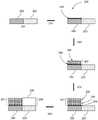
图1示出用于在基板表面101上选择性沉积钝化膜的方法100的反应示意图。基板表面101包括金属表面102(例如Cu、Co、Ni、W、Ru、V、Cr、Fe、Pt、Au、Ag、Mo、Ga和In等的金属)。方法在110处包含对接前驱物104选择性地与金属表面102反应和结合。方法在120处包含金属表面沉积的对接前驱物104与链单体105发生均聚。方法在130处包含重复均聚数次,直到形成厚度在

在一个或多个实施方式中,用于均聚的链单体是通过化学气相沉积(CVD)工艺、循环层沉积(CLD)工艺或原子层沉积(ALD)工艺形成。In one or more embodiments, the chain monomers for homopolymerization are formed by a chemical vapor deposition (CVD) process, a cyclic layer deposition (CLD) process, or an atomic layer deposition (ALD) process.
在一些实施方式中,对接层与至少两种类型的链单体进行杂聚,其中每种类型的链单体交替进行聚合,直到形成厚度在

图2示出用于在基板表面201上选择性沉积钝化膜的方法200的反应示意图。基板表面201包含金属表面202(例如Cu、Co、Ni、W、Ru、V、Cr、Fe、Pt、Au、Ag、Mo、Ga和In等的金属)。方法在210处包含对接前驱物204选择性地与金属表面202反应并结合。然后,金属表面沉积的对接前驱物204分别在220处的方法和230处的方法中与第一链单体205和第二链单体206进行杂聚。在一些实施方式中,杂聚可重复一次或多次,直到钝化膜207的厚度在

图3示出根据一个或多个实施方式的方法300的流程图。在310处,对接前驱物在基板处理区域中流动,并且在320处,对接层选择性地形成在基板金属表面上。在330处,从基板处理区域中去除对接前驱物,并且在340处,链单体在基板处理区域中流动。在350处,对接层聚合以形成钝化膜;并且在360处,从基板处理区域中去除链单体。在370处,重复所述过程直到钝化膜达到目标厚度。FIG. 3 shows a flowchart of a
在一个或多个实施方式中,用于杂聚的链单体是通过化学气相沉积(CVD)工艺、循环层沉积(CLD)工艺或原子层沉积(ALD)工艺提供。In one or more embodiments, the chain monomers for heteropolymerization are provided by a chemical vapor deposition (CVD) process, a cyclic layer deposition (CLD) process, or an atomic layer deposition (ALD) process.
在一些实施方式中,均聚或杂聚的链单体是苯乙烯衍生物。在一些实施方式中,苯乙烯衍生物的聚合通过加热进行。In some embodiments, the homopolymeric or heteropolymeric chain monomer is a styrene derivative. In some embodiments, the polymerization of the styrene derivative is carried out by heating.
在一些实施方式中,均聚或杂聚的链单体是噻吩衍生物。在一些实施方式中,噻吩衍生物包括但不限于噻吩、3,4-乙烯二氧噻吩、噻吩并噻吩、2,2'-联噻吩和3,4-二甲基噻吩。In some embodiments, the homopolymeric or heteropolymeric chain monomer is a thiophene derivative. In some embodiments, thiophene derivatives include, but are not limited to, thiophene, 3,4-ethylenedioxythiophene, thienothiophene, 2,2'-bithiophene, and 3,4-dimethylthiophene.
在一些实施方式中,聚合至少再重复一次。在一些实施方式中,聚合重复多达500次。在一些实施方式中,聚合在1至1000次、1至900次、1至800次、1至700次、1至600次、1至550次、1至500次、1至450次、1至400次、1至350次、1至300次、1至250次、1至200次、1至150次、1至100次或1至50次的范围内重复。In some embodiments, the polymerization is repeated at least one more time. In some embodiments, the polymerization is repeated up to 500 times. In some embodiments, the polymerization is from 1 to 1000 times, 1 to 900 times, 1 to 800 times, 1 to 700 times, 1 to 600 times, 1 to 550 times, 1 to 500 times, 1 to 450 times, 1 to 400, 1 to 350, 1 to 300, 1 to 250, 1 to 200, 1 to 150, 1 to 100, or 1 to 50 repetitions.
在一些实施方式中,钝化膜的厚度在


在一些实施方式中,在沉积介电膜之后去除钝化膜。在一些实施方式中,从基板去除钝化膜。钝化膜可以通过任何合适的选择性蚀刻工艺去除。合适的选择性蚀刻工艺包括但不限于使用氧等离子体和氟等离子体。在一些实施方式中,当使用氧等离子体去除钝化膜时,金属氧化物层形成在金属表面上。在一些实施方式中,形成在金属表面上的金属氧化物层通过使用还原工艺去除。合适的还原工艺包括但不限于使用包含氢或氨的等离子体和包含氢或氨的热退火。在一些实施方式中,氧等离子体、氟等离子体、氢等离子体和氨等离子体可以独立地远程或内部产生,并且导电地耦合或电感地耦合。在一些实施方式中,钝化膜通过将基板顺序暴露于氧等离子体和氢等离子体而去除。In some embodiments, the passivation film is removed after depositing the dielectric film. In some embodiments, the passivation film is removed from the substrate. The passivation film can be removed by any suitable selective etching process. Suitable selective etching processes include, but are not limited to, the use of oxygen plasma and fluorine plasma. In some embodiments, when the passivation film is removed using oxygen plasma, a metal oxide layer is formed on the metal surface. In some embodiments, the metal oxide layer formed on the metal surface is removed using a reduction process. Suitable reduction processes include, but are not limited to, the use of a plasma containing hydrogen or ammonia and thermal annealing containing hydrogen or ammonia. In some embodiments, oxygen plasma, fluorine plasma, hydrogen plasma, and ammonia plasma may be independently generated remotely or internally, and electrically coupled or inductively coupled. In some embodiments, the passivation film is removed by sequentially exposing the substrate to oxygen plasma and hydrogen plasma.
在一些实施方式中,反应区域是在包括多个腔室的模块化系统中,这些腔室执行各种功能,包括基板中心定位和定向、脱气、退火、沉积和/或蚀刻。根据一个或多个实施方式,模块化系统至少包括第一处理腔室和中央传送腔室。中央传送腔室可以容纳机器人,所述机器人可以在处理腔室和负载锁定腔室之间来回传送基板。传送腔室通常保持在真空条件下并提供用于将基板从一个腔室来回传送到另一个腔室和/或来回传送到位于群集工具前端的负载锁定腔室的中间平台。可适用于本公开内容的两个众所周知的模块化系统是

根据一个或多个实施方式,基板连续处于真空或“负载锁定”条件下,并且在从一个腔室移动到下一个腔室时不暴露于环境空气。传送腔室因此处于真空下并且在真空压强下被“抽空”。惰性气体可存在于处理腔室或传送腔室中。在一些实施方式中,惰性气体用于净化或去除一些或所有反应物(例如,反应物)。根据一个或多个实施方式,惰性气体在处理腔室的出口处注入以防止反应物(例如,反应物)从处理腔室移动到传送腔室和/或附加处理腔室。因此,惰性气体流在腔室的出口处形成幕(curtain)。According to one or more embodiments, the substrate is continuously under vacuum or "load lock" conditions and is not exposed to ambient air when moving from one chamber to the next. The transfer chamber is thus under vacuum and "evacuated" at vacuum pressure. The inert gas may be present in the processing chamber or the transfer chamber. In some embodiments, an inert gas is used to purge or remove some or all of the reactants (eg, reactants). According to one or more embodiments, an inert gas is injected at the outlet of the processing chamber to prevent movement of reactants (eg, reactants) from the processing chamber to the transfer chamber and/or additional processing chambers. Thus, the flow of inert gas forms a curtain at the exit of the chamber.
基板能在单个基板沉积腔室中处理,其中在处理另一个基板之前装载、处理和卸载单个基板。基板也能以类似于传送系统的连续方式进行处理,其中多个基板被单独装载到腔室的第一部分中,移动穿过腔室并从腔室的第二部分卸载。腔室的形状和相关的传送系统能形成直线路径或弯曲路径。此外,处理腔室可以是旋转式传送带(carousel),其中多个基板围绕中心轴移动并且在旋转式传送带路径中暴露于沉积、蚀刻、退火、清洁等工艺。Substrates can be processed in a single substrate deposition chamber, where a single substrate is loaded, processed, and unloaded before processing another substrate. Substrates can also be processed in a continuous manner similar to a conveyor system, wherein multiple substrates are individually loaded into a first portion of the chamber, moved through the chamber, and unloaded from a second portion of the chamber. The shape of the chamber and the associated delivery system can create a straight path or a curved path. Additionally, the processing chamber may be a carousel, where multiple substrates move around a central axis and are exposed to deposition, etching, annealing, cleaning, etc. processes in the carousel path.
在处理期间,可加热或冷却基板。这种加热或冷却能通过任何合适的方式来完成,包括但不限于改变基板支承件的温度和使加热或冷却的气体流到基板表面。在一些实施方式中,基板支承件包括加热器/冷却器,加热器/冷却器可被控制以传导地改变基板温度。在一个或多个实施方式中,所用的气体(反应气体或惰性气体)被加热或冷却以局部改变基板温度。在一些实施方式中,加热器/冷却器位于腔室内邻近基板表面处以对流地改变基板温度。During processing, the substrate may be heated or cooled. Such heating or cooling can be accomplished by any suitable means including, but not limited to, changing the temperature of the substrate support and flowing heated or cooled gases to the substrate surface. In some embodiments, the substrate support includes a heater/cooler that can be controlled to conductively vary the substrate temperature. In one or more embodiments, the gas used (reactive gas or inert gas) is heated or cooled to locally alter the substrate temperature. In some embodiments, a heater/cooler is located within the chamber adjacent the substrate surface to convectively change the substrate temperature.
基板在处理期间也可以是静止的或旋转的。旋转的基板能连续地或以离散的步骤旋转(围绕基板轴)。例如,基板可在整个过程中旋转,或者基板可以在暴露于不同反应气体或净化气体之间少量旋转。在处理期间(连续地或分步地)旋转基板可以通过最小化例如气流几何形状的局部变化的影响来帮助产生更均匀的沉积或蚀刻。The substrate can also be stationary or rotating during processing. A rotating substrate can be rotated (about the substrate axis) continuously or in discrete steps. For example, the substrate may be rotated throughout the process, or the substrate may be rotated in small amounts between exposures to different reactive or purge gases. Rotating the substrate during processing (continuously or stepwise) can help produce more uniform deposition or etching by minimizing the effects of local variations in gas flow geometry, for example.
在空间ALD工艺中,反应气体流入处理腔室内的不同处理区域。不同的处理区域与相邻的处理区域分开,以使得反应气体不会混合。基板可在处理区域之间移动以将基板单独地暴露于反应气体。在基板移动期间,基板表面,或基板表面上的材料的不同部分暴露于两种或更多种反应气体,使得基板上的任何给定点基本上不会同时暴露于多于一种反应气体。如本领域技术人员将理解的,由于处理室内的气体扩散,有可能基板的一小部分可能同时暴露于多种反应气体,并且此同时暴露是无意的,除非另有规定。In a spatial ALD process, reactive gases flow into different processing zones within the processing chamber. Different processing zones are separated from adjacent processing zones so that the reactant gases do not mix. The substrates can be moved between processing zones to individually expose the substrates to reactive gases. During movement of the substrate, the substrate surface, or different portions of the material on the substrate surface, are exposed to two or more reactive gases such that any given point on the substrate is not substantially exposed to more than one reactive gas at the same time. As will be understood by those skilled in the art, due to gas diffusion within the processing chamber, it is possible that a small portion of the substrate may be exposed to multiple reactive gases at the same time, and this simultaneous exposure is unintentional unless otherwise specified.
在空间ALD工艺的另一方面中,反应气体同时输送到反应区域,但被惰性气体幕和/或真空幕分隔开。气幕可以是流入处理腔室的惰性气体和流出处理腔室的真空流的组合。基板相对于气体输送装置移动,使得基板上的任何给定点仅暴露于一种反应气体。In another aspect of the spatial ALD process, the reactant gases are delivered to the reaction zone simultaneously, but separated by a curtain of inert gas and/or a vacuum. The gas curtain may be a combination of inert gas flowing into the process chamber and vacuum flow out of the process chamber. The substrate is moved relative to the gas delivery device such that any given point on the substrate is exposed to only one reactive gas.
如本文中所用的“脉冲”或“剂量”是指间歇地或非连续地引入处理腔室中的源气体的量。取决于脉冲的持续时间,每个脉冲内特定化合物的量可随时间变化。特定工艺气体可包括单一化合物或两种或更多种化合物的混合物/组合。As used herein, "pulse" or "dose" refers to the amount of source gas that is intermittently or discontinuously introduced into a processing chamber. Depending on the duration of the pulses, the amount of a particular compound within each pulse can vary over time. A particular process gas may include a single compound or a mixture/combination of two or more compounds.
在一些实施方式的时域ALD工艺中,暴露于每种反应气体(包括但不限于对接前驱物、链单体和将用于介电膜的电介质反应物)被时间延迟分隔以允许每种化合物在基板表面上粘附和/或反应,并且然后从处理腔室中清除。通过在后续暴露之间的处理腔室的清除来防止反应气体混合。In the time domain ALD process of some embodiments, exposure to each reactive gas (including but not limited to docking precursors, chain monomers, and dielectric reactants to be used in the dielectric film) is separated by a time delay to allow each compound Adhesion and/or reaction on the surface of the substrate, and then removal from the processing chamber. Reactive gas mixing is prevented by purging of the processing chamber between subsequent exposures.
在一些实施方式的时域ALD工艺的另一方面中,反应气体脉冲之间存在时间延迟。在每一时间延迟期间,诸如氩气的净化气体被引入处理腔室中以净化反应区域或以其他方式从反应区域去除任何剩余反应气体或反应产物。或者,净化气体可在整个沉积工艺期间连续流动,使得仅净化气体在反应气体的脉冲之间的时间延迟期间流动。反应气体交替地在反应气体之间用净化气体脉冲脉冲化,直到在基板表面上形成

每个脉冲/剂量的持续时间是可变的,并且可被调整以适应例如处理腔室的空间容量以及与处理腔室耦合的真空系统的能力。此外,工艺气体的剂量时间可能会根据工艺气体的流速、工艺气体的温度、控制阀的类型、所使用的处理腔室的类型以及吸附到基板表面上的工艺气体成分的能力而变化。剂量时间也可以基于正在形成的层的类型和正在形成的装置的几何形状而变化。剂量时间应足够长以提供足以吸附/化学吸附到基板的基本整个表面上并在基板的基本整个表面上上形成工艺气体组分层的化合物体积。The duration of each pulse/dose is variable and can be adjusted to accommodate, for example, the space capacity of the processing chamber and the capabilities of the vacuum system coupled to the processing chamber. In addition, the dosing time of the process gas may vary depending on the flow rate of the process gas, the temperature of the process gas, the type of control valve, the type of processing chamber used, and the ability of the process gas components to adsorb onto the substrate surface. The dose time may also vary based on the type of layer being formed and the geometry of the device being formed. The dose time should be long enough to provide a volume of compound sufficient to adsorb/chemisorb onto substantially the entire surface of the substrate and to form a layer of process gas components on substantially the entire surface of the substrate.
一旦沉积钝化膜,所述方法可以任选地包括进一步处理(例如,介电膜的块体沉积)。在一些实施方式中,进一步处理可以是ALD工艺。例如,在一些实施方式中,可以执行ALD工艺以将氮化硅层块体沉积到目标厚度。在多个特定实施方式中,工艺包括使对接前驱物的脉冲流动,随后用氮气和/或氩气清除;流动介电反应物,随后用氮气和/或氩气清除。清除也可以通过施加真空而不流动气体来进行。Once the passivation film is deposited, the method may optionally include further processing (eg, bulk deposition of a dielectric film). In some embodiments, the further processing can be an ALD process. For example, in some embodiments, an ALD process may be performed to bulk deposit a silicon nitride layer to a target thickness. In various specific embodiments, the process includes pulsing the docking precursor, followed by purging with nitrogen and/or argon; flowing dielectric reactants, followed by purging with nitrogen and/or argon. Purging can also be done by applying vacuum without flowing gas.
在一个或多个实施方式中,本文描述的工艺通常可以作为软件程序存储在存储器中,当由控制器或处理器执行时,所述软件程序使基板处理室执行本公开内容中描述的一个或多个工艺。软件程序还可以由第二控制器或处理器(未示出)存储和/或执行,所述第二控制器或处理器远离由控制器或处理器控制的硬件。本公开内容的一些或全部方法也可以在硬件中执行。因此,此工艺可以在软件中实现并使用计算机系统在硬件(例如专用集成电路或其他类型的硬件实现)中执行,或者作为软件和硬件的组合。软件例程在由处理器或控制器执行时,将通用计算机转换为控制腔室操作的专用计算机(控制器),从而执行工艺。这些工艺可以存储在包括指令的非暂时性计算机可读介质上,当由基板处理腔室的控制器执行时,所述指令使基板处理腔室执行本文描述的一种或多种方法。In one or more embodiments, the processes described herein may generally be stored in memory as a software program that, when executed by a controller or processor, causes a substrate processing chamber to perform one or more of the methods described in this disclosure. Multiple processes. The software program may also be stored and/or executed by a second controller or processor (not shown) remote from the hardware controlled by the controller or processor. Some or all of the methods of the present disclosure may also be implemented in hardware. Thus, the process may be implemented in software and performed in hardware using a computer system (eg, an application specific integrated circuit or other type of hardware implementation), or as a combination of software and hardware. Software routines, when executed by a processor or controller, convert a general-purpose computer into a special-purpose computer (controller) that controls the operation of the chamber to perform the process. These processes may be stored on a non-transitory computer readable medium comprising instructions that, when executed by a controller of a substrate processing chamber, cause the substrate processing chamber to perform one or more of the methods described herein.
在本说明书中,对“一个实施方式”、“某些实施方式”、“一个或多个实施方式”或“一实施方式”的引用意味着结合实施方式描述的特定特征、结构、材料或特性包含在至少一个本公开内容的实施方式中。因此,在本说明书的各个位置出现诸如“在一个或多个实施方式中”、“在某些实施方式中”、“在一个实施方式中”或“在一实施方式中”之类的短语不一定指代本公开内容的相同实施方式。此外,在一个或多个实施方式中,特定特征、结构、材料或特性可以任何适当的方式结合。In this specification, references to "one embodiment," "some embodiments," "one or more embodiments," or "an embodiment" mean a particular feature, structure, material, or characteristic described in connection with the embodiments Included in at least one embodiment of the present disclosure. Thus, the appearance of phrases such as "in one or more embodiments", "in some embodiments", "in one embodiment" or "in an embodiment" in various places in this specification does not The same embodiments of the present disclosure must be referred to. Furthermore, the particular features, structures, materials or characteristics may be combined in any suitable manner in one or more embodiments.
尽管已参考多个特定实施方式描述了本文的公开内容,但是应当理解,这些实施方式仅仅是对本公开内容的原理和应用的说明。对于本领域技术人员来说显而易见的是,在不脱离本公开内容的精神和范围的情况下,可对本公开内容的方法和设备进行各种修改和变化。因此,本公开内容旨在包括在所附权利要求书和所附权利要求书的等效物的范围内的修改和变化。Although the disclosure herein has been described with reference to a number of specific embodiments, it should be understood that these embodiments are merely illustrative of the principles and applications of the present disclosure. It will be apparent to those skilled in the art that various modifications and variations can be made in the method and apparatus of the present disclosure without departing from the spirit and scope of the disclosure. Accordingly, the present disclosure is intended to include modifications and changes within the scope of the appended claims and equivalents of the appended claims.
Claims (20)


Applications Claiming Priority (3)
| Application Number | Priority Date | Filing Date | Title |
|---|---|---|---|
| US17/081,482US11621161B2 (en) | 2020-10-27 | 2020-10-27 | Selective deposition of a passivation film on a metal surface |
| US17/081,482 | 2020-10-27 | ||
| PCT/US2021/056624WO2022093801A1 (en) | 2020-10-27 | 2021-10-26 | Selective deposition of a passivation film on a metal surface |
Publications (2)
| Publication Number | Publication Date |
|---|---|
| CN114981472Atrue CN114981472A (en) | 2022-08-30 |
| CN114981472B CN114981472B (en) | 2024-09-06 |
Family
ID=81257504
Family Applications (1)
| Application Number | Title | Priority Date | Filing Date |
|---|---|---|---|
| CN202180003878.9AActiveCN114981472B (en) | 2020-10-27 | 2021-10-26 | Selective deposition of passivation films on metal surfaces |
Country Status (4)
| Country | Link |
|---|---|
| US (1) | US11621161B2 (en) |
| KR (1) | KR102641933B1 (en) |
| CN (1) | CN114981472B (en) |
| WO (1) | WO2022093801A1 (en) |
Families Citing this family (7)
| Publication number | Priority date | Publication date | Assignee | Title |
|---|---|---|---|---|
| TWI757565B (en)* | 2017-12-22 | 2022-03-11 | 美商應用材料股份有限公司 | Methods for depositing blocking layers on conductive surfaces |
| US20230197418A1 (en)* | 2021-12-20 | 2023-06-22 | International Business Machines Corporation | Selective deposition enabled by vapor phase inhibitor |
| US20240120195A1 (en)* | 2022-10-06 | 2024-04-11 | Applied Materials, Inc. | Dielectric on dielectric selective deposition using aniline passivation |
| US12394620B2 (en)* | 2022-10-28 | 2025-08-19 | Applied Materials, Inc. | Benzyl compound passivation for selective deposition and selective etch protection |
| US20240242946A1 (en)* | 2023-01-18 | 2024-07-18 | Sky Tech Inc. | Low power plasma system monitor method |
| US12438050B2 (en) | 2023-02-14 | 2025-10-07 | Applied Materials, Inc. | Electronic device fabrication using area-selective deposition |
| US20240420996A1 (en)* | 2023-06-13 | 2024-12-19 | Applied Materials, Inc. | Selective self-assembled monolayer (sam) removal |
Citations (6)
| Publication number | Priority date | Publication date | Assignee | Title |
|---|---|---|---|---|
| US20040115921A1 (en)* | 2002-12-11 | 2004-06-17 | International Business Machines Corporation | Method for depositing a metal layer on a semiconductor interconnect structure having a capping layer |
| CN102822949A (en)* | 2010-03-30 | 2012-12-12 | 东京毅力科创株式会社 | Surface cleaning and selective deposition of metal-containing cap layers for semiconductor devices |
| CN107208262A (en)* | 2014-11-21 | 2017-09-26 | 应用材料公司 | Alcohols auxiliary ALD film deposition |
| TW201925513A (en)* | 2017-11-14 | 2019-07-01 | 美商應用材料股份有限公司 | Enhanced selective deposition process |
| CN110892508A (en)* | 2017-07-18 | 2020-03-17 | 应用材料公司 | Method for depositing barrier layers on metal surfaces |
| CN111094622A (en)* | 2017-12-22 | 2020-05-01 | 伊鲁米纳公司 | Fracture passivation in a matrix |
Family Cites Families (8)
| Publication number | Priority date | Publication date | Assignee | Title |
|---|---|---|---|---|
| FR2829046B1 (en)* | 2001-08-28 | 2005-01-14 | Commissariat Energie Atomique | METHOD OF GRAFTING AND GROWING A CONDUCTIVE ORGANIC FILM ON A SURFACE |
| DE102004022674A1 (en)* | 2004-05-07 | 2005-11-24 | H.C. Starck Gmbh | Electrolytic condenser for use in electronic circuits, e.g. for computers, comprises porous electrode, dielectric, solid electrolyte and a layer containing a polymeric anion, a polyaniline or polythiophene and a binder |
| PT1524678E (en)* | 2003-10-17 | 2009-10-19 | Starck H C Gmbh | Electrolytic capacitors with polymeric outer layer |
| US9490145B2 (en)* | 2015-02-23 | 2016-11-08 | Asm Ip Holding B.V. | Removal of surface passivation |
| US10900120B2 (en)* | 2017-07-14 | 2021-01-26 | Asm Ip Holding B.V. | Passivation against vapor deposition |
| TWI765080B (en) | 2017-08-13 | 2022-05-21 | 美商應用材料股份有限公司 | Method of enhancing selective deposition by cross-linking of blocking molecules |
| US20190316256A1 (en) | 2018-04-13 | 2019-10-17 | Applied Materials, Inc. | Methods Of Selective Atomic Layer Deposition |
| JP7146690B2 (en)* | 2018-05-02 | 2022-10-04 | エーエスエム アイピー ホールディング ビー.ブイ. | Selective layer formation using deposition and removal |
- 2020
- 2020-10-27USUS17/081,482patent/US11621161B2/enactiveActive
- 2021
- 2021-10-26WOPCT/US2021/056624patent/WO2022093801A1/ennot_activeCeased
- 2021-10-26KRKR1020217040630Apatent/KR102641933B1/enactiveActive
- 2021-10-26CNCN202180003878.9Apatent/CN114981472B/enactiveActive
Patent Citations (7)
| Publication number | Priority date | Publication date | Assignee | Title |
|---|---|---|---|---|
| US20040115921A1 (en)* | 2002-12-11 | 2004-06-17 | International Business Machines Corporation | Method for depositing a metal layer on a semiconductor interconnect structure having a capping layer |
| CN102822949A (en)* | 2010-03-30 | 2012-12-12 | 东京毅力科创株式会社 | Surface cleaning and selective deposition of metal-containing cap layers for semiconductor devices |
| CN107208262A (en)* | 2014-11-21 | 2017-09-26 | 应用材料公司 | Alcohols auxiliary ALD film deposition |
| CN110892508A (en)* | 2017-07-18 | 2020-03-17 | 应用材料公司 | Method for depositing barrier layers on metal surfaces |
| US20200234943A1 (en)* | 2017-07-18 | 2020-07-23 | Applied Materials, Inc. | Methods For Depositing Blocking Layers On Metal Surfaces |
| TW201925513A (en)* | 2017-11-14 | 2019-07-01 | 美商應用材料股份有限公司 | Enhanced selective deposition process |
| CN111094622A (en)* | 2017-12-22 | 2020-05-01 | 伊鲁米纳公司 | Fracture passivation in a matrix |
Also Published As
| Publication number | Publication date |
|---|---|
| KR20220058852A (en) | 2022-05-10 |
| WO2022093801A1 (en) | 2022-05-05 |
| CN114981472B (en) | 2024-09-06 |
| US20220130664A1 (en) | 2022-04-28 |
| KR102641933B1 (en) | 2024-02-27 |
| US11621161B2 (en) | 2023-04-04 |
Similar Documents
| Publication | Publication Date | Title |
|---|---|---|
| CN114981472B (en) | Selective deposition of passivation films on metal surfaces | |
| US20170114465A1 (en) | Methods Of Depositing Flowable Films Comprising SiO and SiN | |
| KR102775083B1 (en) | Area-selective atomic layer deposition of passivation layers | |
| US20200243323A1 (en) | Methods for depositing silicon nitride | |
| US20240271272A1 (en) | Semiconductor device patterning methods | |
| CN113373429A (en) | Molecular layer deposition of amorphous carbon films | |
| CN114761613B (en) | Selective deposition of passivation films | |
| TW202342787A (en) | Area selective carbon-based film deposition | |
| KR20150125674A (en) | CATALYTIC ATOMIC LAYER DEPOSITION OF FILMS COMPRISING SiOC | |
| CN117120664A (en) | Reducing agent for atomic layer deposition | |
| US20220108881A1 (en) | Method and system for forming silicon nitride on a sidewall of a feature | |
| TW202142722A (en) | Molecular layer deposition of amorphous carbon films | |
| CN116964714A (en) | Deposition of silicon-based dielectric films | |
| WO2025207415A1 (en) | In situ acyclic diamino carbene (adc) deposition |
Legal Events
| Date | Code | Title | Description |
|---|---|---|---|
| PB01 | Publication | ||
| PB01 | Publication | ||
| SE01 | Entry into force of request for substantive examination | ||
| SE01 | Entry into force of request for substantive examination | ||
| GR01 | Patent grant | ||
| GR01 | Patent grant |