CN114977812A - A switching power supply high voltage power supply circuit and device - Google Patents
A switching power supply high voltage power supply circuit and deviceDownload PDFInfo
- Publication number
- CN114977812A CN114977812ACN202210387070.1ACN202210387070ACN114977812ACN 114977812 ACN114977812 ACN 114977812ACN 202210387070 ACN202210387070 ACN 202210387070ACN 114977812 ACN114977812 ACN 114977812A
- Authority
- CN
- China
- Prior art keywords
- resistor
- diode
- pin
- voltage
- power supply
- Prior art date
- Legal status (The legal status is an assumption and is not a legal conclusion. Google has not performed a legal analysis and makes no representation as to the accuracy of the status listed.)
- Pending
Links
Images


Classifications
- H—ELECTRICITY
- H02—GENERATION; CONVERSION OR DISTRIBUTION OF ELECTRIC POWER
- H02M—APPARATUS FOR CONVERSION BETWEEN AC AND AC, BETWEEN AC AND DC, OR BETWEEN DC AND DC, AND FOR USE WITH MAINS OR SIMILAR POWER SUPPLY SYSTEMS; CONVERSION OF DC OR AC INPUT POWER INTO SURGE OUTPUT POWER; CONTROL OR REGULATION THEREOF
- H02M3/00—Conversion of DC power input into DC power output
- H02M3/22—Conversion of DC power input into DC power output with intermediate conversion into AC
- H02M3/24—Conversion of DC power input into DC power output with intermediate conversion into AC by static converters
- H02M3/26—Conversion of DC power input into DC power output with intermediate conversion into AC by static converters using discharge tubes without control electrode or semiconductor devices without control electrode to produce the intermediate AC
- H—ELECTRICITY
- H02—GENERATION; CONVERSION OR DISTRIBUTION OF ELECTRIC POWER
- H02M—APPARATUS FOR CONVERSION BETWEEN AC AND AC, BETWEEN AC AND DC, OR BETWEEN DC AND DC, AND FOR USE WITH MAINS OR SIMILAR POWER SUPPLY SYSTEMS; CONVERSION OF DC OR AC INPUT POWER INTO SURGE OUTPUT POWER; CONTROL OR REGULATION THEREOF
- H02M1/00—Details of apparatus for conversion
- Y—GENERAL TAGGING OF NEW TECHNOLOGICAL DEVELOPMENTS; GENERAL TAGGING OF CROSS-SECTIONAL TECHNOLOGIES SPANNING OVER SEVERAL SECTIONS OF THE IPC; TECHNICAL SUBJECTS COVERED BY FORMER USPC CROSS-REFERENCE ART COLLECTIONS [XRACs] AND DIGESTS
- Y02—TECHNOLOGIES OR APPLICATIONS FOR MITIGATION OR ADAPTATION AGAINST CLIMATE CHANGE
- Y02B—CLIMATE CHANGE MITIGATION TECHNOLOGIES RELATED TO BUILDINGS, e.g. HOUSING, HOUSE APPLIANCES OR RELATED END-USER APPLICATIONS
- Y02B70/00—Technologies for an efficient end-user side electric power management and consumption
- Y02B70/10—Technologies improving the efficiency by using switched-mode power supplies [SMPS], i.e. efficient power electronics conversion e.g. power factor correction or reduction of losses in power supplies or efficient standby modes
Landscapes
- Engineering & Computer Science (AREA)
- Power Engineering (AREA)
- Dc-Dc Converters (AREA)
Abstract
Translated fromChinese
Description
Translated fromChinese技术领域technical field
本申请涉及电子技术领域,尤其涉及一种开关电源高压供电电路及装置。The present application relates to the field of electronic technology, and in particular, to a switching power supply high-voltage power supply circuit and device.
背景技术Background technique
通用串行总线技术(Universal Serial Bus,USB)是当今生活中应用最广泛的通信接口之一。除了快速的数据传输功能之外,USB还能够为其适配的设备提供可靠的电源连接。目前多数电子设备都能够使用USB充电器为其充电,且伴随着技术的进步,充电速度也越来越快。USB充电器基于开关电源技术将市电转换为电子设备所需的充电电压,通常采用的电路拓扑为反激变换器。其一次侧的控制芯片需要一定的工作电压来保持正常工作,而该工作电压一般由一次侧高压或者变压器上的辅助绕组提供。Universal Serial Bus (Universal Serial Bus, USB) is one of the most widely used communication interfaces in today's life. In addition to fast data transfer capabilities, USB can also provide a reliable power connection for the devices it adapts to. At present, most electronic devices can be charged with USB chargers, and with the advancement of technology, the charging speed is getting faster and faster. The USB charger converts the commercial power into the charging voltage required by the electronic device based on the switching power supply technology, and the circuit topology usually used is a flyback converter. The control chip on the primary side needs a certain working voltage to keep working normally, and the working voltage is generally provided by the high voltage on the primary side or the auxiliary winding on the transformer.
但是,一方面,高压供电的方式需要串接电阻,长久地供电会提升整体损耗;另一方面,随着功率需求的提升,即输出电压的提高,辅助绕组上的电压也会随之变大,由辅助绕组供电难以满足高输出电压时的芯片引脚耐压要求。However, on the one hand, the high-voltage power supply method requires series resistance, and the long-term power supply will increase the overall loss; on the other hand, as the power demand increases, that is, the output voltage increases, the voltage on the auxiliary winding will also increase accordingly. , it is difficult to meet the chip pin withstand voltage requirements at high output voltage by supplying power from the auxiliary winding.
发明内容SUMMARY OF THE INVENTION
本申请提供了一种开关电源高压供电电路及装置,能够减少高压供电时的功率损耗,降低电路设计的成本。The present application provides a switching power supply high-voltage power supply circuit and device, which can reduce power loss during high-voltage power supply and reduce the cost of circuit design.
第一方面,本申请实施例提供了一种开关电源高压供电电路,所述电路包括整流电路、第一二极管、第二二极管、芯片、第一电阻RHV,所述芯片包括供电电压输入VDD引脚、高压输入HV引脚以及开关管,其中,所述整流电路的第一输入端与所述第一二极管的正极连接,所述整流电路的第二输入端与所述第二二极管的正极连接,所述第一二极管的负极、所述第二二极管的负极与所述第一电阻RHV的一端连接,所述第一电阻RHV的另一端与所述HV引脚连接,所述HV引脚与所述开关管的第一极连接,所述开关管的第二极与所述VDD引脚连接。In a first aspect, an embodiment of the present application provides a switching power supply high-voltage power supply circuit, the circuit includes a rectifier circuit, a first diode, a second diode, a chip, and a first resistor RHV , and the chip includes a power supply A voltage input VDD pin, a high voltage input HV pin and a switch tube, wherein the first input end of the rectifier circuit is connected to the anode of the first diode, and the second input end of the rectifier circuit is connected to the The anode of the second diode is connected, the cathode of the first diode and the cathode of the second diode are connected to one end of the first resistor RHV , and the other end of the first resistor RHV connected with the HV pin, the HV pin is connected with the first pole of the switch tube, and the second pole of the switch tube is connected with the VDD pin.
在本申请实施例中,通过检测供电电压输入VDD引脚的电压值,从而驱动芯片以及整个开关电源工作,通过比较高压输入HV引脚的电压值与一恒定边界值,从而导通或断开开关管,实现电压稳定的开关电源高压供电,同时减少高压供电时的功率损耗。In the embodiment of the present application, by detecting the voltage value of the power supply voltage input to the VDD pin, the chip and the entire switching power supply are driven to work, and by comparing the voltage value of the high voltage input HV pin with a constant boundary value, it is turned on or off. Switch tube, realize the high voltage power supply of switching power supply with stable voltage, and reduce the power loss during high voltage power supply.
在一种可能的设计中,所述电路还包括第一电容CVDD,其中,所述VDD引脚与所述第一电容CVDD的一端连接,所述第一电容CVDD的另一端接地。In a possible design, the circuit further includes a first capacitor CVDD , wherein the VDD pin is connected to one end of the first capacitor CVDD and the other end of the first capacitor CVDD is grounded.
在一种可能的设计中,所述电路还包括第二电阻Ra1、第三电阻Ra2以及辅助绕组AUX,所述芯片还包括检测VS引脚、地线GND引脚,其中,所述VS引脚与所述第二电阻Ra1的一端以及所述第三电阻Ra2的一端连接,所述第二电阻Ra1的另一端与所述辅助绕组AUX的同名端连接,所述辅助绕组AUX的异名端接地,所述第三电阻Ra2的另一端接地,所述GND引脚接地。In a possible design, the circuit further includes a second resistor Ra1 , a third resistor Ra2 and an auxiliary winding AUX, and the chip further includes a detection VS pin and a ground GND pin, wherein the VS The pin is connected to one end of the second resistor Ra1 and one end of the third resistor Ra2 , and the other end of the second resistor Ra1 is connected to the same-named end of the auxiliary winding AUX, the auxiliary winding AUX The other end of the third resistor Ra2 is grounded, and the GND pin is grounded.
在一种可能的设计中,所述电路还包括第四电阻Rcs、开关、变压器、第二电容Cin、第三二极管D1,第三电容Cout,所述芯片还包括采样信号CS引脚、功率管GATE引脚,其中,所述整流电路的输出端与所述第二电容Cin的一端以及所述变压器的初级异名端连接,所述变压器的初级同名端与所述开关的第一极连接,所述开关的第二极与所述GATE引脚连接,所述开关的第三极与所述CS引脚以及所述第四电阻Rcs的一端连接,所述第四电阻Rcs的另一端接地,所述第二电容Cin的另一端接地,所述变压器的次级同名端与所述第三二极管D1的正极连接,所述第三二极管D1的负极与所述第三电容Cout的一端以及输出电压Uout连接,所述变压器的次级异名端与所述第三电容Cout的另一端接地。In a possible design, the circuit further includes a fourth resistor Rcs , a switch, a transformer, a second capacitor Cin , a third diode D1 , and a third capacitor Cout , and the chip further includes a sampling signal CS pin, power tube GATE pin, wherein the output end of the rectifier circuit is connected to one end of the second capacitor Cin and the primary synonym end of the transformer, and the primary synonym end of the transformer is connected to the The first pole of the switch is connected, the second pole of the switch is connected to the GATE pin, the third pole of the switch is connected to the CS pin and one end of the fourth resistor Rcs , the The other end of the four resistors Rcs is grounded, the other end of the second capacitor Cin is grounded, the secondary end of the transformer is connected to the anode of the third diode D1 , and the third diode The negative electrode of D1 is connected to one end of the third capacitor Cout and the output voltage Uout , and the secondary end of the transformer is grounded to the other end of the third capacitor Cout .
在一种可能的设计中,所述整流电路包括第四二极管、第五二极管、第六二极管以及第七二极管,其中,所述整流电路的第一输入端与所述第四二极管的正极以及所述第五二极管的负极连接,所述整流电路的第二输入端与所述第六二极管的正极以及所述第七二极管的负极连接,所述第四二极管的负极、所述第六二极管的负极与所述整流电路的输出端连接,所述第五二极管的正极与所述第七二极管的正极接地。In a possible design, the rectifier circuit includes a fourth diode, a fifth diode, a sixth diode and a seventh diode, wherein the first input end of the rectifier circuit is connected to the The anode of the fourth diode and the cathode of the fifth diode are connected, and the second input end of the rectifier circuit is connected to the anode of the sixth diode and the cathode of the seventh diode , the cathode of the fourth diode and the cathode of the sixth diode are connected to the output end of the rectifier circuit, and the anode of the fifth diode and the anode of the seventh diode are grounded .
在本申请实施例中,整流电路的第一输入端接入交流电路的输入端,利用二极管的单向导通性使电路中的电流只按单向流动,在整流电路的每个工作周期内,同一时间只有两个二极管(第四二极管和第七二极管,或,第五二极管和第六二极管)进行工作,从而使整流电路的输出端得到直流电。In the embodiment of the present application, the first input end of the rectifier circuit is connected to the input end of the AC circuit, and the unidirectional conductivity of the diode is used to make the current in the circuit only flow in one direction. Only two diodes (the fourth diode and the seventh diode, or the fifth diode and the sixth diode) work at the same time, so that the output terminal of the rectifier circuit obtains direct current.
在一种可能的设计中,所述电路还包括第五电阻CFB和光敏三极管,所述芯片还包括电流反馈输入FB引脚,所述FB引脚与所述第五电阻CFB的一端以及所述光敏三极管的集电极连接,所述第五电阻CFB的另一端和所述光敏三极管的发射端接地。In a possible design, the circuit further includes a fifth resistor CFB and a phototransistor, the chip further includes a current feedback input FB pin, the FB pin is connected to one end of the fifth resistor CFB and The collector of the phototransistor is connected, and the other end of the fifth resistor CFB and the emitter of the phototransistor are grounded.
在一种可能的设计中,所述电路还包括第六电阻RH、第七电阻Rb1、第八电阻Rb2、光敏二极管、第九电阻R1、第四电容C1、第十电阻RL以及稳压二极管,其中,所述第七电阻Rb1的一端与所述第六电阻RH的一端以及所述第三电容Cout的一端连接,所述第七电阻Rb1的另一端与所述光敏二极管的正极以及所述第八电阻Rb2的一端连接,所述光敏二极管的负极以及所述第八电阻Rb2的另一端与所述稳压二极管的负极、所述第九电阻R1的一端连接,所述第九电阻R1的另一端与所述第四电容C1的一端连接,所述第四电容C1的另一端分别与所述稳压二极管的正极、所述第十电阻RL的一端以及所述第六电阻RH的另一端连接,所述第十电阻RL的另一端与所述稳压二极管的正极接地。In a possible design, the circuit further includes a sixth resistor RH , a seventh resistor Rb1 , an eighth resistor Rb2 , a photodiode, a ninth resistor R1 , a fourth capacitor C1 , and a tenth resistor RL and a Zener diode, wherein one end of the seventh resistor Rb1 is connected to one end of the sixth resistorRH and one end of the third capacitor Cout , and the other end of the seventh resistor Rb1 is connected to The anode of the photodiode and one end of the eighth resistor Rb2 are connected, and the cathode of the photodiode and the other end of the eighth resistor Rb2 are connected to the cathode of the zener diode and the ninth resistor R1 is connected to one end, the other end of the ninth resistor R1 is connected toone end of the fourth capacitorC1 , and the other end of the fourth capacitorC1 is connected to the positive electrode of the Zener diode, the One end of the tenth resistorRL and the other end of the sixth resistorRH are connected, and the other end of the tenth resistorRL is grounded with the anode of the zener diode.
在一种可能的设计中,所述开关管为高耐压开关管。In a possible design, the switch tube is a high withstand voltage switch tube.
第二方面,本申请实施例提供了一种电源装置,该装置包括第一方面提供的开关电源高压供电电路。In a second aspect, an embodiment of the present application provides a power supply device, which includes the switching power supply high-voltage power supply circuit provided in the first aspect.
附图说明Description of drawings
为了更清楚地说明本申请实施例或背景技术中的技术方案,下面将对本申请实施例或背景技术中所需要使用的附图进行说明。In order to more clearly illustrate the technical solutions in the embodiments of the present application or the background technology, the accompanying drawings required in the embodiments or the background technology of the present application will be described below.
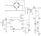
图1是本申请实施例提供的一种开关电源高压供电电路的结构示意图;1 is a schematic structural diagram of a switching power supply high-voltage power supply circuit provided by an embodiment of the present application;
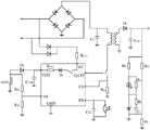
图2是本申请实施例提供的一种开关电源高压供电电路的结构示意图;2 is a schematic structural diagram of a switching power supply high-voltage power supply circuit provided by an embodiment of the present application;
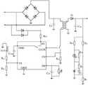
图3是本申请实施例提供的一种开关电源高压供电电路的结构示意图;3 is a schematic structural diagram of a switching power supply high-voltage power supply circuit provided by an embodiment of the present application;
图4是本申请实施例提供的一种开关电源高压供电电路的结构示意图;4 is a schematic structural diagram of a switching power supply high-voltage power supply circuit provided by an embodiment of the present application;
图5是本申请实施例提供的一种电压波形示意图。FIG. 5 is a schematic diagram of a voltage waveform provided by an embodiment of the present application.
具体实施方式Detailed ways
下面结合本申请实施例中的附图对本申请实施例进行描述。The embodiments of the present application will be described below with reference to the accompanying drawings in the embodiments of the present application.
请参见图1,图1是本申请实施例提供的一种开关电源高压供电电路的结构示意图,所述电路包括:整流电路、第一电容Cin、第一电阻RHV1、第二电阻RHV2以及芯片,所述芯片包括供电电压输入VDD引脚、高压输入HV引脚,其中,所述整流电路的输出端与所述第一电容Cin的一端以及第一电阻RHV1的一端连接,所述第一电容Cin的另一端接地,所述第一电阻RHV1的另一端与所述第二电阻RHV2的一端连接,所述第二电阻RHV2的另一端与所述HV引脚连接,所述HV引脚与所述VDD引脚连接。Please refer to FIG. 1 . FIG. 1 is a schematic structural diagram of a switching power supply high-voltage power supply circuit provided by an embodiment of the present application. The circuit includes: a rectifier circuit, a first capacitor Cin , a first resistor RHV1 , and a second resistor RHV2 and a chip, the chip includes a power supply voltage input VDD pin and a high voltage input HV pin, wherein the output end of the rectifier circuit is connected to one end of the first capacitor Cin and one end of the first resistor RHV1 , so The other end of the first capacitor Cin is grounded, the other end of the first resistance RHV1 is connected with one end of the second resistance RHV2 , and the other end of the second resistance RHV2 is connected with the HV pin , the HV pin is connected to the VDD pin.
进一步的,所述开关电源高压供电电路还包括第二电容CVDD、第一二极管D2、第三电阻Ra1、第四电阻Ra2、辅助绕组AUX,所述芯片还包括检测VS引脚,其中,所述VDD引脚与所述第二电容CVDD的一端以及所述第一二极管D2的负极连接,所述第二电容CVDD的另一端接地,所述第一二极管D2的正极与所述辅助绕组AUX的同名端以及所述第三电阻Ra1的一端连接,所述第三电阻Ra1的另一端与所述VS引脚以及所述第四电阻Ra2的一端连接,所述第四电阻Ra2的另一端与所述辅助绕组AUX的异名端接地。Further, the switching power supply high-voltage power supply circuit further includes a second capacitor CVDD , a first diode D2 , a third resistor Ra1 , a fourth resistor Ra2 , and an auxiliary winding AUX, and the chip further includes a detection VS lead. pin, wherein the VDD pin is connected to one end of the second capacitor CVDD and the negative electrode of the first diode D2 , the other end of the second capacitor CVDD is grounded, and the first twoThe positive pole of the pole tube D2 is connected to the same-named end of the auxiliary winding AUX and one end of the third resistor Ra1 , and the other end of the third resistor Ra1 is connected to the VS pin and the fourth resistor R One end ofa2 is connected, and the other end of the fourth resistor Ra2 is grounded with the opposite end of the auxiliary winding AUX.
在如图1所示的电路结构中,芯片中的供电电压输入VDD引脚和高压输入HV引脚通过导线连通,该电路中为芯片供电主要包括以下两条供电线路:一条为经整流电路、一次侧电压(变压器的输入端侧)、第一电阻RHV1、第二电阻RHV2、高压输入HV引脚、供电电压输入VDD引脚的高压供电线路,该线路直接连接交流电,并将市电转换为芯片工作的供电电压;另一条为由辅助绕组AUX、第一二极管D2至第二电容CVDD的供电线路,该线路由辅助绕组AUX上的电压为芯片工作供电。In the circuit structure shown in Figure 1, the power supply voltage input VDD pin and the high voltage input HV pin in the chip are connected by wires. The power supply for the chip in this circuit mainly includes the following two power supply lines: one is a rectified circuit, The primary side voltage (input side of the transformer), the first resistor RHV1 , the second resistor RHV2 , the high voltage input HV pin, the high voltage power supply line of the power supply voltage input VDD pin, the line is directly connected to the AC power, and the mains Converted to the power supply voltage for chip work; the other is the power supply line from the auxiliary winding AUX, the first diode D2 to the second capacitor CVDD , and the line is powered by the voltage on the auxiliary winding AUX for chip work.
具体地,在启动或其它启用高压供电方式时,高压供电线路连通,交流电经过整流电路转换为直流电后,经过串联的第一电阻RHV1和第二电阻RHV2时,因为受启动速度的限制,阻值不能过大,在第一电阻RHV1和第二电阻RHV2上会产生额外的功率,造成整个高压供电过程中的功率损耗。Specifically, during startup or other enabling high-voltage power supply methods, the high-voltage power supply line is connected, and after the alternating current is converted into direct current through the rectifier circuit, when the first resistor RHV1 and the second resistor RHV2 are connected in series, due to the limitation of the startup speed, The resistance value cannot be too large, extra power will be generated on the first resistor RHV1 and the second resistor RHV2 , resulting in power loss during the entire high-voltage power supply process.
进一步的,所述开关电源高压供电电路还包括变压器、开关、第五电阻Rcs、第二二极管D1、第三电容Cout,所述芯片还包括采样信号CS引脚、功率管GATE引脚,其中,所述第一电阻RHV1的一端与所述变压器的初级异名端连接,所述变压器的初级同名端与所述开关的第一极连接,所述开关的第二极与所述GATE引脚连接,所述开关的第三极与所述CS引脚以及所述第五电阻Rcs的一端连接,所述第五电阻Rcs的另一端接地,所述变压器的次级同名端与所述第二二极管D1的正极连接,所述第二二极管D1的负极与所述第三电容Cout的一端以及输出电压Uout连接,所述变压器的次级异名端与所述第三电容Cout的另一端接地。Further, the switching power supply high-voltage power supply circuit further includes a transformer, a switch, a fifth resistor Rcs , a second diode D1 , and a third capacitor Cout , and the chip further includes a sampling signal CS pin, a power transistor GATE pin, wherein one end of the first resistor RHV1 is connected to the primary synonymous end of the transformer, the primary synonymous end of the transformer is connected to the first pole of the switch, and the second pole of the switch is connected to the first pole of the switch. The GATE pin is connected, the third pole of the switch is connected to the CS pin and one end of the fifth resistor Rcs , the other end of the fifth resistor Rcs is grounded, and the secondary of the transformer is connected to the ground. The terminal of the same name is connected to the anode of the second diode D1, the cathodeof the second diode D1 is connected toone end of the third capacitorCout and the output voltage Uout, and the secondary of the transformer The synonym terminal is grounded with the other terminal of the third capacitor Cout .
具体地,在正常工作时,GATE引脚驱动开关动作,此时,电路初级侧的线圈为变压器初级侧线圈和辅助绕组AUX的线圈,电路次级侧线圈为变压器次级侧线圈,当开关关断时,辅助绕组AUX上的电压UAUX与输出电压Uout呈现倍数关系,使得在高输出电压的情况下,芯片的供电电压输入VDD引脚上的电压UVDD值也过高,容易超过引脚标准的耐受电压值,从而导致芯片损坏。Specifically, during normal operation, the GATE pin drives the switch to act. At this time, the coil on the primary side of the circuit is the coil on the primary side of the transformer and the coil on the auxiliary winding AUX, and the coil on the secondary side of the circuit is the coil on the secondary side of the transformer. When the switch is off When it is off, the voltage UAUX on the auxiliary winding AUX has a multiple relationship with the output voltage Uout , so that in the case of high output voltage, the voltage UVDD on the input VDD pin of the power supply voltage of the chip is also too high, which is easy to exceed the lead voltage. pin standard withstand voltage value, resulting in chip damage.
请参见图2,图2是本申请实施例提供的一种开关电源高压供电电路的结构示意图,所述电路包括:整流电路、第一二极管、第二二极管、芯片、第一电阻RHV1,所述芯片包括供电电压输入VDD引脚、高压输入HV引脚、开关管、第二电阻RHV2、第三二极管D3,其中,所述整流电路的第一输入端与所述第一二极管的正极连接,所述整流电路的第二输入端与所述第二二极管的正极连接,所述第一二极管的负极、所述第二二极管的负极与所述第一电阻RHV1的一端连接,所述第一电阻RHV1的另一端与所述HV引脚连接,所述HV引脚与所述开关管的第一极连接,所述开关管的第二极与所述第三二极管D3的正极连接,所述第三二极管D3的负极与所述第二电阻RHV2的一端连接,所述第二电阻RHV2的另一端与所述VDD引脚连接。Please refer to FIG. 2. FIG. 2 is a schematic structural diagram of a switching power supply high-voltage power supply circuit provided by an embodiment of the present application. The circuit includes: a rectifier circuit, a first diode, a second diode, a chip, and a first resistor RHV1 , the chip includes a power supply voltage input VDD pin, a high voltage input HV pin, a switch tube, a second resistor RHV2 , and a third diode D3 , wherein the first input end of the rectifier circuit is connected to the The anode of the first diode is connected, the second input end of the rectifier circuit is connected to the anode of the second diode, the cathode of the first diode, and the cathode of the second diode Connect with one end of the first resistor RHV1 , the other end of the first resistor RHV1 is connected with the HV pin, the HV pin is connected with the first pole of the switch tube, the switch tube The second pole is connected to the anode of thethird diodeD3 , the cathode of the third diode D3 is connected to one end of the second resistor RHV2 , and the other end of the second resistor RHV2 One end is connected to the VDD pin.
进一步的,所述开关电源高压供电电路还包括第一电容CVDD、第四二极管D2、第三电阻Ra1、第四电阻Ra2、辅助绕组AUX,所述芯片还包括检测VS引脚,其中,所述VDD引脚与所述第一电容CVDD的一端以及所述第四二极管D2的负极连接,所述第一电容CVDD的另一端接地,所述第四二极管D2的正极与所述辅助绕组AUX的同名端以及所述第三电阻Ra1的一端连接,所述第三电阻Ra1的另一端与所述VS引脚以及所述第四电阻Ra2的一端连接,所述第四电阻Ra2的另一端与所述辅助绕组AUX的异名端接地。Further, the switching power supply high-voltage power supply circuit further includes a first capacitor CVDD , a fourth diode D2 , a third resistor Ra1 , a fourth resistor Ra2 , and an auxiliary winding AUX, and the chip further includes a detection VS lead. pin, wherein the VDD pin is connected to one end of the first capacitor CVDD and the negative electrode of the fourth diode D2 , the other end of the first capacitor CVDD is grounded, and the fourth and secondThe positive pole of the pole tube D2 is connected to the same-named end of the auxiliary winding AUX and one end of the third resistor Ra1 , and the other end of the third resistor Ra1 is connected to the VS pin and the fourth resistor R One end ofa2 is connected, and the other end of the fourth resistor Ra2 is grounded with the opposite end of the auxiliary winding AUX.
在如图2所示的电路结构中,与图1所述的电路结构相比较,该电路中增加了第一二极管和第二二极管,并将两个二极管作为整流管分别接入到整流电路的第一输入端和第二输入端(即输入交流电源的第一输入端和第二输入端),将串联的第一电阻RHV1和第二电阻RHV2改为仅第一电阻RHV1接入HV引脚,并将第二电阻RHV2、第三二极管D3以及开关管接入到芯片内部的高压输入HV引脚、供电电压输入VDD引脚之间,其中,开关管为高耐压开关管。该电路中为芯片供电主要包括以下两条供电线路:一条为经整流管(第一二极管和第二二极管)、第一电阻RHV1、高压输入HV引脚、开关管、第三二极管D3、第二电阻RHV2、供电电压输入VDD引脚的高压供电线路,该线路直接连接交流电,并将市电转换为芯片工作的供电电压;另一条为由辅助绕组AUX、第四二极管D2至第一电容CVDD的供电线路,该线路由辅助绕组AUX上的电压为芯片工作供电,其中,高压供电为芯片供电的主要供电方式,并由开关管控制高压供电线路的连通和断开。In the circuit structure shown in FIG. 2, compared with the circuit structure shown in FIG. 1, a first diode and a second diode are added to the circuit, and the two diodes are connected as rectifiers respectively. To the first input terminal and the second input terminal of the rectifier circuit (that is, the first input terminal and the second input terminal of the input AC power supply), change the series connected first resistor RHV1 and second resistor RHV2 to only the first resistor RHV1 is connected to the HV pin, and the second resistor RHV2 , the third diode D3 and the switch tube are connected between the high-voltage input HV pin and the power supply voltage input VDD pin inside the chip, wherein the switch The tube is a high pressure switch tube. The power supply for the chip in this circuit mainly includes the following two power supply lines: one is the rectifier tube (the first diode and the second diode), the first resistor RHV1 , the high voltage input HV pin, the switch tube, the third The diode D3 , the second resistor RHV2 , and the high-voltage power supply line whose power supply voltage is input to the VDD pin is directly connected to the alternating current, and converts the commercial power into the power supply voltage for the chip to work; The power supply line from the four diodes D2 to the first capacitor CVDD , the line is powered by the voltage on the auxiliary winding AUX to supply power for the chip, wherein the high-voltage power supply is the main power supply mode for power supply of the chip, and the high-voltage power supply line is controlled by the switch tube connection and disconnection.
具体地,在高压供电时,开关管处于连通状态,交流电经高压供电线路直至VDD引脚,VDD引脚处的电压UVDD达到电压预设值,启动芯片和整个开关电源开始正常工作;正常工作时,交流电经高压供电线路中的整流管(第一二极管和第二二极管)、第一电阻RHV1到达HV引脚,检测HV引脚上的电压UHV,当电压UHV小于电压UVDD边界值时,判断为电压UHV的谷底区间,此时,连通开关管进行高压充电;当电压UHV大于电压UVDD边界值时,断开开关管停止供电。此外,当辅助绕组上的电压UAUX大于电压UVDD时,可关闭高压供电线路,仅由辅助绕组AUX供电。Specifically, when the high-voltage power supply is used, the switch tube is in a connected state, the alternating current passes through the high-voltage power supply line to the VDD pin, the voltage UVDD at the VDD pin reaches the voltage preset value, and the startup chip and the entire switching power supply start to work normally; When the AC power reaches the HV pin through the rectifier tube (the first diode and the second diode) and the first resistor RHV1 in the high-voltage power supply line, the voltage UHV on the HV pin is detected, and when the voltage UHV is less than When the voltage UVDD boundary value is determined as the valley interval of the voltage UHV , at this time, the switch tube is connected to perform high-voltage charging; when the voltage UHV is greater than the voltage UVDD boundary value, the switch tube is disconnected to stop power supply. In addition, when the voltage UAUX on the auxiliary winding is greater than the voltage UVDD , the high-voltage power supply line can be turned off, and only the auxiliary winding AUX is powered.
在电压UHV的谷底区间进行充电时,电压UVDD随着电压UHV的增大呈波动式上升,由于每个周期的充电量不确定,因此需要设定电压UVDD的上、下边界值(Utop、Ubottom),使电压UVDD处于上、下边界值中间,避免电压UVDD超出正常的工作电压范围。此外,为保证每个周期的充电量充足,需要根据芯片工作时电压UVDD的动态值调整上、下边界值,但电压UVDD的上、下边界值及其相应的逻辑判定电路的设计和动态调整都增加了芯片设计的复杂度和成本。When charging in the valley interval of the voltage UHV , the voltage UVDD fluctuates with the increase of the voltage UHV . Since the charging amount of each cycle is uncertain, it is necessary to set the upper and lower boundary values of the voltage UVDD . (Utop , Ubottom ), so that the voltage UVDD is in the middle of the upper and lower boundary values, so as to prevent the voltage UVDD from exceeding the normal working voltage range. In addition, in order to ensure sufficient charging capacity in each cycle, it is necessary to adjust the upper and lower boundary values according to the dynamic value of the voltage UVDD when the chip is working, but the upper and lower boundary values of the voltage UVDD and the design of the corresponding logic judgment circuit Both dynamic adjustments increase the complexity and cost of chip design.
因此,基于以上现有技术中存在的问题,本申请实施例提供一种开关电源高压供电电路及装置,能够减少高压供电时带来的额外功率损耗以及辅助绕组供电的过压风险,同时降低了额外器件以及逻辑判定电路带来的设计成本。Therefore, based on the above problems in the prior art, the embodiments of the present application provide a switching power supply high-voltage power supply circuit and device, which can reduce the extra power loss caused by the high-voltage power supply and the overvoltage risk of the auxiliary winding power supply, and at the same time reduce the Design costs caused by additional components and logic decision circuits.
请参见图3,图3是本申请实施例提供的一种开关电源高压供电电路的结构示意图,所述电路包括:整流电路、第一二极管、第二二极管、芯片、第一电阻RHV,所述芯片包括供电电压输入VDD引脚、高压输入HV引脚以及开关管,其中,所述整流电路的第一输入端与所述第一二极管的正极连接,所述整流电路的第二输入端与所述第二二极管的正极连接,所述第一二极管的负极、所述第二二极管的负极与所述第一电阻RHV的一端连接,所述第一电阻RHV的另一端与所述HV引脚连接,所述HV引脚与所述开关管的第一极连接,所述开关管的第二极与所述VDD引脚连接。Please refer to FIG. 3. FIG. 3 is a schematic structural diagram of a switching power supply high-voltage power supply circuit provided by an embodiment of the present application. The circuit includes: a rectifier circuit, a first diode, a second diode, a chip, and a first resistor RHV , the chip includes a power supply voltage input VDD pin, a high voltage input HV pin and a switch tube, wherein the first input end of the rectifier circuit is connected to the anode of the first diode, and the rectifier circuit The second input terminal of the R HV is connected to the anode of the second diode, the cathode of the first diode and the cathode of the second diode are connected to one end of the first resistor RHV , the The other end of the first resistor RHV is connected to the HV pin, the HV pin is connected to the first pole of the switch tube, and the second pole of the switch tube is connected to the VDD pin.
在如图3所示的电路结构中,芯片中的供电电压输入VDD引脚和高压输入HV引脚通过开关管连通,其中,开关管可以为高耐压开关管,第一二极管和第二二极管可以为整流二极管,其组成的整流管分别接入到整流电路的第一输入端和第二输入端,将交流电源转换为直流电源。该电路中芯片供电线路主要为经整流管(第一二极管和第二二极管)、第一电阻RHV、HV引脚、开关管、VDD引脚的高压供电线路,其中,整流管的输入端(第一二极管的正极和第二二极管的正极)连接至开关电源的交流电源输入端,整流管的输出端(第一二极管的负极和第二二极管的负极)连接第一电阻RHV的一端,第一电阻RHV的另一端连接芯片的HV引脚,在芯片内部高耐压开关管的漏极(第一极)与HV引脚相连,源极(第二极)与VDD引脚相连。In the circuit structure shown in FIG. 3 , the power supply voltage input VDD pin and the high voltage input HV pin in the chip are connected through a switch tube, wherein the switch tube can be a high withstand voltage switch tube, the first diode and the third The two diodes can be rectifier diodes, and the rectifier tubes formed by them are respectively connected to the first input end and the second input end of the rectifier circuit to convert the AC power supply into the DC power supply. The chip power supply line in this circuit is mainly a high-voltage power supply line through the rectifier tube (the first diode and the second diode), the first resistor RHV , the HV pin, the switch tube, and the VDD pin. Among them, the rectifier tube The input terminal of the rectifier tube (the anode of the first diode and the anode of the second diode) is connected to the AC power input terminal of the switching power supply, and the output terminal of the rectifier tube (the cathode of the first diode and the anode of the second diode) Negative electrode) is connected to one end of the first resistor RHV , the other end of the first resistor RHV is connected to the HV pin of the chip, the drain (the first pole) of the high withstand voltage switch tube inside the chip is connected to the HV pin, and the source (Second pole) is connected to the VDD pin.
进一步的,请参见图4,图4是本申请实施例提供的一种开关电源高压供电电路的结构示意图,图4所述电路还包括第一电容CVDD,其中,所述VDD引脚与所述第一电容CVDD的一端连接,所述第一电容CVDD的另一端接地。Further, please refer to FIG. 4 , which is a schematic structural diagram of a switching power supply high-voltage power supply circuit provided by an embodiment of the present application. The circuit shown in FIG. 4 further includes a first capacitor CVDD , wherein the VDD pin is connected to all One end of the first capacitor CVDD is connected to the ground, and the other end of the first capacitor CVDD is grounded.
应理解,该开关电源高压供电电路的供电方法包括但不限于以下两个过程:It should be understood that the power supply method of the switching power supply high voltage power supply circuit includes but is not limited to the following two processes:
1、电路通电时,芯片内部的高耐压开关管保持导通,电流经高压供电线路持续流向第一电容CVDD,VDD引脚处的电压UVDD持续上升,检测电压UVDD值,当电压UVDD值小于预设的边界值Uboundary(边界值Uboundary恒定)时,芯片中的其他部分不工作,芯片的功率管GATE引脚处无驱动电压输出;当电压UVDD值大于或等于预设的边界值Uboundary时,芯片以及整个开关电源开始正常工作。1. When the circuit is powered on, the high-voltage switch tube inside the chip remains on, the current continues to flow to the first capacitor CVDD through the high-voltage power supply line, the voltage UVDD at the VDD pin continues to rise, and the value of the voltage UVDD is detected. When the UVDD value is less than the preset boundary value Uboundary (the boundary value Uboundary is constant), other parts of the chip do not work, and there is no driving voltage output at the GATE pin of the power tube of the chip; when the voltage UVDD value is greater than or equal to the preset value When the boundary value Uboundary is set, the chip and the entire switching power supply start to work normally.
2、正常工作时,检测芯片HV引脚处的电压UHV值,判断是否导通高耐压开关管进行高压充电。假设初始时,高耐压开关管处于断开状态,此时,经整流管输出端的电压Urec值与HV引脚处的电压UHV值相同,当电压UHV值小于预设的边界值Uboundary时,芯片驱动高耐压开关管导通,进行高压充电,当高耐压开关管导通后,因芯片的HV引脚与VDD引脚直接相连,HV引脚处的电压UHV值会迅速降至与VDD引脚处的电压UVDD值相等,此时电压Urec值和电压UHV值(电压UVDD值)偏差较小,且随后电压Urec值会迅速降至谷底(0V),使得充电时间过短,因此电压Urec值下降阶段的充电可忽略不计,同时因整流管的限制,第一电容CVDD并不会向交流电源处反向放电。2. During normal operation, detect the voltage UHV value at the HV pin of the chip, and judge whether the high-voltage switch tube is turned on for high-voltage charging. Assuming that the high withstand voltage switch tube is in an off state initially, at this time, the voltage Urec value of the output terminal of the rectifier tube is the same as the voltage UHV value at the HV pin, when the voltage UHV value is less than the preset boundary value U At theboundary , the chip drives the high-voltage switch tube to conduct high-voltage charging. When the high-voltage switch tube is turned on, because the HV pin of the chip is directly connected to the VDD pin, the voltage UHV value at the HV pin will change. Rapidly drops to the same value as the voltage UVDD at the VDD pin, at this time the voltage Urec value and the voltage UHV value (voltage UVDD value) have a small deviation, and then the voltage Urec value will quickly drop to the bottom (0V) , so that the charging time is too short, so the charging in the falling stage of the voltage Urec can be ignored, and at the same time, due to the limitation of the rectifier tube, the first capacitor CVDD will not discharge reversely to the AC power source.
接着,电压Urec值开始上升并达到电压UHV值(电压UVDD值),因第一电阻RHV阻值不大,电压UHV值(电压UVDD值)会随着电压Urec值迅速上升至预设的边界值Uboundary,完成高压充电。Then, the value of voltage Urec starts to rise and reaches the value of voltage UHV (value of voltage UVDD ). Since the resistance value of the first resistor RHV is not large, the value of voltage UHV (value of voltage UVDD ) will follow the value of voltage Urec rapidly. It rises to the preset boundary value Uboundary to complete high voltage charging.
当电压UHV值大于预设的边界值Uboundary时,芯片驱动高耐压开关管断开,停止高压供电,此时,电压UHV值和电压UVDD值不再同步变化,电压UHV值将继续随着电压Urec值变化,电压UVDD值因维持芯片工作缓慢下降。具体过程如图5所示,图5是本申请实施例提供的一种电压波形示意图,主要充电过程发生在电压Urec值上升阶段t1-t2时间段内。When the voltage UHV value is greater than the preset boundary value Uboundary , the chip drives the high-voltage switch tube to disconnect, and stops the high-voltage power supply. At this time, the voltage UHV value and the voltage UVDD value no longer change synchronously, and the voltage UHV value It will continue to change with the value of the voltage Urec , and the value of the voltage UVDD will decrease slowly to maintain the chip operation. The specific process is shown in FIG. 5 , which is a schematic diagram of a voltage waveform provided by an embodiment of the present application. The main charging process occurs in the time period t1-t2 of the rising stage of the voltage Urec value.
可选的,所述电路还包括第二电阻Ra1、第三电阻Ra2以及辅助绕组AUX,所述芯片还包括检测VS引脚、地线GND引脚,其中,所述VS引脚与所述第二电阻Ra1的一端以及所述第三电阻Ra2的一端连接,所述第二电阻Ra1的另一端与所述辅助绕组AUX的同名端连接,所述辅助绕组AUX的异名端接地,所述第三电阻Ra2的另一端接地,所述GND引脚接地。Optionally, the circuit further includes a second resistor Ra1 , a third resistor Ra2 and an auxiliary winding AUX, and the chip further includes a detection VS pin and a ground wire GND pin, wherein the VS pin is connected to all of them. One end of the second resistor Ra1 and one end of the third resistor Ra2 are connected, and the other end of the second resistor Ra1 is connected to the same name end of the auxiliary winding AUX, and the different name end of the auxiliary winding AUX Grounding, the other end of the third resistor Ra2 is grounded, and the GND pin is grounded.
可选的,所述电路还包括第四电阻Rcs、开关、变压器、第二电容Cin、第三二极管D1,第三电容Cout,所述芯片还包括采样信号CS引脚、功率管GATE引脚,其中,所述整流电路的输出端与所述第二电容Cin的一端以及所述变压器的初级异名端连接,所述变压器的初级同名端与所述开关的第一极连接,所述开关的第二极与所述GATE引脚连接,所述开关的第三极与所述CS引脚以及所述第四电阻Rcs的一端连接,所述第四电阻Rcs的另一端接地,所述第二电容Cin的另一端接地,所述变压器的次级同名端与所述第三二极管D1的正极连接,所述第三二极管D1的负极与所述第三电容Cout的一端以及输出电压Uout连接,所述变压器的次级异名端与所述第三电容Cout的另一端接地。Optionally, the circuit further includes a fourth resistor Rcs , a switch, a transformer, a second capacitor Cin , a third diode D1 , and a third capacitor Cout , and the chip further includes a sampling signal CS pin, GATE pin of the power tube, wherein the output end of the rectifier circuit is connected to one end of the second capacitor Cin and the primary synonymous end of the transformer, and the primary synonymous end of the transformer is connected to the first end of the switch The second pole of the switch is connected to the GATE pin, the third pole of the switch is connected to the CS pin and one end of the fourth resistor Rcs , the fourth resistor Rcs The other end of the second capacitor Cin is grounded, the secondary end of the transformer is connected to the anode of the third diode D1 , and the cathode of the third diode D1 is connected to the ground. It is connected to one end of the third capacitor Cout and the output voltage Uout , and the secondary end of the transformer is grounded to the other end of the third capacitor Cout .
可选的,所述整流电路包括第四二极管、第五二极管、第六二极管以及第七二极管,其中,所述整流电路的第一输入端与所述第四二极管的正极以及所述第五二极管的负极连接,所述整流电路的第二输入端与所述第六二极管的正极以及所述第七二极管的负极连接,所述第四二极管的负极、所述第六二极管的负极与所述整流电路的输出端连接,所述第五二极管的正极与所述第七二极管的正极接地。Optionally, the rectifier circuit includes a fourth diode, a fifth diode, a sixth diode and a seventh diode, wherein the first input end of the rectifier circuit is connected to the fourth and second diodes. The anode of the diode is connected to the cathode of the fifth diode, the second input end of the rectifier circuit is connected to the anode of the sixth diode and the cathode of the seventh diode, and the second input terminal of the rectifier circuit is connected to the anode of the sixth diode and the cathode of the seventh diode. The cathode of the fourth diode and the cathode of the sixth diode are connected to the output end of the rectifier circuit, and the anode of the fifth diode is grounded to the anode of the seventh diode.
可选的,所述电路还包括第五电阻CFB和光敏三极管,所述芯片还包括电流反馈输入FB引脚,所述FB引脚与所述第五电阻CFB的一端以及所述光敏三极管的集电极连接,所述第五电阻CFB的另一端和所述光敏三极管的发射端接地。Optionally, the circuit further includes a fifth resistor CFB and a phototransistor, the chip further includes a current feedback input FB pin, the FB pin and one end of the fifth resistor CFB and the phototransistor. The collector is connected, and the other end of the fifth resistor CFB and the emitter of the phototransistor are grounded.
可选的,所述电路还包括第六电阻RH、第七电阻Rb1、第八电阻Rb2、光敏二极管、第九电阻R1、第四电容C1、第十电阻RL以及稳压二极管,其中,所述第七电阻Rb1的一端与所述第六电阻RH的一端以及所述第三电容Cout的一端连接,所述第七电阻Rb1的另一端与所述光敏二极管的正极以及所述第八电阻Rb2的一端连接,所述光敏二极管的负极以及所述第八电阻Rb2的另一端与所述稳压二极管的负极、所述第九电阻R1的一端连接,所述第九电阻R1的另一端与所述第四电容C1的一端连接,所述第四电容C1的另一端分别与所述稳压二极管的正极、所述第十电阻RL的一端以及所述第六电阻RH的另一端连接,所述第十电阻RL的另一端与所述稳压二极管的正极接地。Optionally, the circuit further includes a sixth resistor RH , a seventh resistor Rb1 , an eighth resistor Rb2 , a photodiode, a ninth resistor R1 , a fourth capacitor C1 , a tenth resistor RL and a voltage regulator diode, wherein one end of the seventh resistor Rb1 is connected to one end of the sixth resistorRH and one end of the third capacitor Cout , and the other end of the seventh resistor Rb1 is connected to the photodiode The anode of the photodiode and one end of the eighth resistor Rb2 are connected, the cathode of the photodiode and the other end of the eighth resistor Rb2 are connected to the cathode of the zener diode and one end of the ninth resistor R1 , the other end of the ninth resistor R1 is connected to one end of the fourth capacitor C1 , and the other end of the fourth capacitor C1 is respectively connected to the positive electrode of the Zener diode and the tenth resistor RL One end of the resistor RH is connected to the other end of the sixth resistorRH , and the other end of the tenth resistorRL is grounded to the anode of the Zener diode.
可选的,所述开关管为高耐压开关管。Optionally, the switch tube is a high-voltage switch tube.
在本申请实施例中,每个周期内的充电都是在电压UHV值(电压UVDD值)上升至预设的边界值Uboundary时结束,即每个周期内的充电都能确保电压UVDD值达到所需的电压值(Uboundary),因此,在正常工作时,电压UVDD值始终能够稳定在预设的边界值Uboundary下方,维持平稳的波动。In the embodiment of the present application, the charging in each cycle ends when the voltage UHV value (voltage UVDD value) rises to the preset boundary value Uboundary , that is, the charging in each cycle can ensure the voltage U TheVDD value reaches the required voltage value (Uboundary ), therefore, during normal operation, the voltage UVDD value can always be stable below the preset boundary value Uboundary to maintain stable fluctuations.
本申请实施例还提供了一种电源装置,所述装置包括如上述图1-图3中任一所述的开关电源高压供电电路。An embodiment of the present application further provides a power supply device, which includes the switching power supply high-voltage power supply circuit as described in any of the above-mentioned FIG. 1 to FIG. 3 .
以上所述的具体实施方式,对本发明的目的、技术方案和有益效果进行了进一步详细说明。凡在本发明的精神和原则之内,所作的任何修改、等同替换、改进等,均应包含在本发明的保护范围之内。The specific embodiments described above further describe the objectives, technical solutions and beneficial effects of the present invention in detail. Any modification, equivalent replacement, improvement, etc. made within the spirit and principle of the present invention shall be included within the protection scope of the present invention.
Claims (10)
Priority Applications (2)
| Application Number | Priority Date | Filing Date | Title |
|---|---|---|---|
| CN202210387070.1ACN114977812A (en) | 2022-04-14 | 2022-04-14 | A switching power supply high voltage power supply circuit and device |
| PCT/CN2023/088273WO2023198170A1 (en) | 2022-04-14 | 2023-04-14 | High-voltage power supply circuit and apparatus for switching power supply |
Applications Claiming Priority (1)
| Application Number | Priority Date | Filing Date | Title |
|---|---|---|---|
| CN202210387070.1ACN114977812A (en) | 2022-04-14 | 2022-04-14 | A switching power supply high voltage power supply circuit and device |
Publications (1)
| Publication Number | Publication Date |
|---|---|
| CN114977812Atrue CN114977812A (en) | 2022-08-30 |
Family
ID=82977520
Family Applications (1)
| Application Number | Title | Priority Date | Filing Date |
|---|---|---|---|
| CN202210387070.1APendingCN114977812A (en) | 2022-04-14 | 2022-04-14 | A switching power supply high voltage power supply circuit and device |
Country Status (2)
| Country | Link |
|---|---|
| CN (1) | CN114977812A (en) |
| WO (1) | WO2023198170A1 (en) |
Cited By (1)
| Publication number | Priority date | Publication date | Assignee | Title |
|---|---|---|---|---|
| WO2023198170A1 (en)* | 2022-04-14 | 2023-10-19 | 深圳英集芯科技股份有限公司 | High-voltage power supply circuit and apparatus for switching power supply |
Citations (1)
| Publication number | Priority date | Publication date | Assignee | Title |
|---|---|---|---|---|
| US20180316273A1 (en)* | 2017-04-28 | 2018-11-01 | Weltrend Semiconductor Inc. | Switching Mode Power Supply with Dynamic High-Voltage Charging to Maintain Operating Voltage |
Family Cites Families (5)
| Publication number | Priority date | Publication date | Assignee | Title |
|---|---|---|---|---|
| JP6822024B2 (en)* | 2016-09-09 | 2021-01-27 | 富士電機株式会社 | Control circuit of switching power supply |
| CN112054657B (en)* | 2020-09-04 | 2022-06-07 | 昂宝电子(上海)有限公司 | Pulse width modulation control chip and power conversion system |
| CN214506884U (en)* | 2021-03-11 | 2021-10-26 | 佛山市南海赛威科技技术有限公司 | Power converter and power control chip |
| CN114977812A (en)* | 2022-04-14 | 2022-08-30 | 深圳英集芯科技股份有限公司 | A switching power supply high voltage power supply circuit and device |
| CN114552957B (en)* | 2022-04-26 | 2022-07-22 | 深圳英集芯科技股份有限公司 | Power supply circuit of switching power supply and power supply method thereof |
- 2022
- 2022-04-14CNCN202210387070.1Apatent/CN114977812A/enactivePending
- 2023
- 2023-04-14WOPCT/CN2023/088273patent/WO2023198170A1/ennot_activeCeased
Patent Citations (1)
| Publication number | Priority date | Publication date | Assignee | Title |
|---|---|---|---|---|
| US20180316273A1 (en)* | 2017-04-28 | 2018-11-01 | Weltrend Semiconductor Inc. | Switching Mode Power Supply with Dynamic High-Voltage Charging to Maintain Operating Voltage |
Cited By (1)
| Publication number | Priority date | Publication date | Assignee | Title |
|---|---|---|---|---|
| WO2023198170A1 (en)* | 2022-04-14 | 2023-10-19 | 深圳英集芯科技股份有限公司 | High-voltage power supply circuit and apparatus for switching power supply |
Also Published As
| Publication number | Publication date |
|---|---|
| WO2023198170A1 (en) | 2023-10-19 |
Similar Documents
| Publication | Publication Date | Title |
|---|---|---|
| CN105763078B (en) | Switching Power Supply and bus capacitor voltage control method for Switching Power Supply | |
| CN206321756U (en) | Power failure detection circuit and switching power supply circuit | |
| CN104124878B (en) | Power supply module, switching power source chip and switch power supply system | |
| TWI551016B (en) | Power supply and power supply method | |
| CN106953533A (en) | Flyback power supply circuit and electrical equipment | |
| CN114552957B (en) | Power supply circuit of switching power supply and power supply method thereof | |
| TWI633426B (en) | Power supply system and method | |
| CN114189155A (en) | Power adapter with ultra-low standby power | |
| CN112311220A (en) | PFC control circuit and power control device | |
| CN114977812A (en) | A switching power supply high voltage power supply circuit and device | |
| CN111384844B (en) | A power supply circuit for suppressing instantaneous inrush current when starting up | |
| CN106992671A (en) | Power supply and power supply method | |
| CN110707945A (en) | Rectifier circuit, wireless charging device, power supply equipment and wireless charging system | |
| CN101154824A (en) | Charger circuit with output voltage compensation | |
| CN217883244U (en) | Equipment power supply control circuit | |
| CN112014621A (en) | A current detection circuit, switching power supply and TV set | |
| TW201441785A (en) | Power adaptor apparatus | |
| WO2016031843A1 (en) | Charger | |
| CN204441852U (en) | A kind of three-phase overvoltage, under-voltage, phase shortage integrated protective circuit | |
| CN103973099B (en) | Electronic device, power converter and method of operation thereof | |
| CN110476319A (en) | Charging unit | |
| CN201868933U (en) | A primary-side feedback constant-voltage current-limiting RCC charger control circuit | |
| CN216414153U (en) | Conversion circuit and power transmission controller with dummy load | |
| CN205881143U (en) | A remote control transmitter circuit used in series with a DC motor controller | |
| CN220382938U (en) | Power supply with ring field effect transistor |
Legal Events
| Date | Code | Title | Description |
|---|---|---|---|
| PB01 | Publication | ||
| PB01 | Publication | ||
| SE01 | Entry into force of request for substantive examination | ||
| SE01 | Entry into force of request for substantive examination |