CN114977792A - Switching Frequency Control Circuit - Google Patents
Switching Frequency Control CircuitDownload PDFInfo
- Publication number
- CN114977792A CN114977792ACN202210550083.6ACN202210550083ACN114977792ACN 114977792 ACN114977792 ACN 114977792ACN 202210550083 ACN202210550083 ACN 202210550083ACN 114977792 ACN114977792 ACN 114977792A
- Authority
- CN
- China
- Prior art keywords
- pwm
- control module
- current
- signal
- voltage
- Prior art date
- Legal status (The legal status is an assumption and is not a legal conclusion. Google has not performed a legal analysis and makes no representation as to the accuracy of the status listed.)
- Pending
Links
Images


Classifications
- H—ELECTRICITY
- H02—GENERATION; CONVERSION OR DISTRIBUTION OF ELECTRIC POWER
- H02M—APPARATUS FOR CONVERSION BETWEEN AC AND AC, BETWEEN AC AND DC, OR BETWEEN DC AND DC, AND FOR USE WITH MAINS OR SIMILAR POWER SUPPLY SYSTEMS; CONVERSION OF DC OR AC INPUT POWER INTO SURGE OUTPUT POWER; CONTROL OR REGULATION THEREOF
- H02M3/00—Conversion of DC power input into DC power output
- H02M3/02—Conversion of DC power input into DC power output without intermediate conversion into AC
- H02M3/04—Conversion of DC power input into DC power output without intermediate conversion into AC by static converters
- H02M3/10—Conversion of DC power input into DC power output without intermediate conversion into AC by static converters using discharge tubes with control electrode or semiconductor devices with control electrode
- H02M3/145—Conversion of DC power input into DC power output without intermediate conversion into AC by static converters using discharge tubes with control electrode or semiconductor devices with control electrode using devices of a triode or transistor type requiring continuous application of a control signal
- H02M3/155—Conversion of DC power input into DC power output without intermediate conversion into AC by static converters using discharge tubes with control electrode or semiconductor devices with control electrode using devices of a triode or transistor type requiring continuous application of a control signal using semiconductor devices only
- H02M3/156—Conversion of DC power input into DC power output without intermediate conversion into AC by static converters using discharge tubes with control electrode or semiconductor devices with control electrode using devices of a triode or transistor type requiring continuous application of a control signal using semiconductor devices only with automatic control of output voltage or current, e.g. switching regulators
- H—ELECTRICITY
- H02—GENERATION; CONVERSION OR DISTRIBUTION OF ELECTRIC POWER
- H02M—APPARATUS FOR CONVERSION BETWEEN AC AND AC, BETWEEN AC AND DC, OR BETWEEN DC AND DC, AND FOR USE WITH MAINS OR SIMILAR POWER SUPPLY SYSTEMS; CONVERSION OF DC OR AC INPUT POWER INTO SURGE OUTPUT POWER; CONTROL OR REGULATION THEREOF
- H02M1/00—Details of apparatus for conversion
- H02M1/14—Arrangements for reducing ripples from DC input or output
- Y—GENERAL TAGGING OF NEW TECHNOLOGICAL DEVELOPMENTS; GENERAL TAGGING OF CROSS-SECTIONAL TECHNOLOGIES SPANNING OVER SEVERAL SECTIONS OF THE IPC; TECHNICAL SUBJECTS COVERED BY FORMER USPC CROSS-REFERENCE ART COLLECTIONS [XRACs] AND DIGESTS
- Y02—TECHNOLOGIES OR APPLICATIONS FOR MITIGATION OR ADAPTATION AGAINST CLIMATE CHANGE
- Y02B—CLIMATE CHANGE MITIGATION TECHNOLOGIES RELATED TO BUILDINGS, e.g. HOUSING, HOUSE APPLIANCES OR RELATED END-USER APPLICATIONS
- Y02B70/00—Technologies for an efficient end-user side electric power management and consumption
- Y02B70/10—Technologies improving the efficiency by using switched-mode power supplies [SMPS], i.e. efficient power electronics conversion e.g. power factor correction or reduction of losses in power supplies or efficient standby modes
Landscapes
- Engineering & Computer Science (AREA)
- Power Engineering (AREA)
- Dc-Dc Converters (AREA)
Abstract
Translated fromChinese
Description
Translated fromChinese技术领域technical field
本发明涉及开关电源技术领域,尤其涉及一种开关频率控制电路。The invention relates to the technical field of switching power supplies, in particular to a switching frequency control circuit.
背景技术Background technique
DC-DC开关电源有多种控制模式。根据采样信号,一般可以分为电压模、电流模。电压模通过采样输出电压进行负反馈,电流模通过采样输入电流和输出电压进行负反馈。常用电流模架构包括:峰值电流模(Peak-CurrentMode),平均电流模(Average-CurrentMode)和滞环电流模(Hysteretic-CurrentMode);按照占空比调制方式来分包括脉宽调制(PulseWidthModulation,PWM),脉冲频率调制(Pulse FrequencyModulation,PFM),恒定导通时间模式(ConstantOnTime,COT),固定关断时间模式(Fixed OffTime,FOT),迟滞控制(Bang-Bang)等模式。DC-DC switching power supply has a variety of control modes. According to the sampling signal, it can be generally divided into voltage mode and current mode. The voltage mode performs negative feedback by sampling the output voltage, and the current mode performs negative feedback by sampling the input current and output voltage. Commonly used current mode architectures include: peak current mode (Peak-CurrentMode), average current mode (Average-CurrentMode) and hysteretic current mode (Hysteretic-CurrentMode); ), Pulse Frequency Modulation (PFM), Constant On Time (COT), Fixed Off Time (FOT), Hysteresis Control (Bang-Bang) and other modes.
其中,COT模式响应速度很快,但传统COT的定时器单元所产生的导通时间(TON)是定值,且开关频率随输入电压、输出电压以及负载电流变化,其开关频率的不稳定使得系统滤波器设计难度很大,再者,传统的COT控制模式的纹波较大,系统的EMI特性比较差,对EMI处理的设计难度加大。Among them, the COT mode has a fast response speed, but the on-time (TON) generated by the traditional COT timer unit is a fixed value, and the switching frequency changes with the input voltage, output voltage and load current. The instability of the switching frequency makes the switching frequency unstable. The design of the system filter is very difficult. Furthermore, the ripple of the traditional COT control mode is relatively large, and the EMI characteristics of the system are relatively poor, which increases the difficulty in designing the EMI processing.
而FOT模式的导通时间则会随着负载的加大而加长来增加占空比,缺点是固定关断时间不能设置过低,过低的话,在较轻载或者输入输出电压接近的时候,频率比较高,效率降低。The on-time of the FOT mode will increase with the increase of the load to increase the duty cycle. The disadvantage is that the fixed off-time cannot be set too low. The higher the frequency, the lower the efficiency.
综上所述,现有技术存在以下缺陷:To sum up, the prior art has the following defects:
1.通过模拟方案来实现导通时间的调节,方案较复杂;1. The on-time adjustment is realized through the simulation scheme, and the scheme is more complicated;
2.模拟方案较容易受到噪声等外界参数的干扰;2. The simulation scheme is more susceptible to the interference of external parameters such as noise;
3.需要用很大的模拟滤波器来获取开关节点sw的平均电压,实现起来不但费芯片面积,且精度或者速度不高。3. It is necessary to use a large analog filter to obtain the average voltage of the switching node sw, which not only costs the chip area, but also has low precision or speed.
特别是,对于混合电流模+时间控制的结构,虽然能够获得非常稳定的环路响应,不需要提供斜坡补偿信号也不会产生次谐波震荡,但是由于牺牲了频率不固定,所以没办法获得较为稳定而精确的开关频率。In particular, for the structure of mixed current mode + time control, although a very stable loop response can be obtained, there is no need to provide a slope compensation signal and no sub-harmonic oscillation will occur, but due to the sacrifice of frequency instability, there is no way to obtain more stable and precise switching frequency.
发明内容SUMMARY OF THE INVENTION
本发明提供一种开关频率控制电路,以解决现有的开关电源控制时无法获得稳定而精确的开关频率的问题。The present invention provides a switching frequency control circuit to solve the problem that a stable and accurate switching frequency cannot be obtained when the existing switching power supply is controlled.
根据本发明的第一方面,提供了一种开关频率控制电路,包括:According to a first aspect of the present invention, a switching frequency control circuit is provided, comprising:
开关电源、PWM控制模块、开关导通控制模块以及数字模块;其中:Switching power supply, PWM control module, switch conduction control module and digital module; wherein:
所述开关电源包括第一开关支路及第二开关支路;所述第一开关支路的第一端连接输入电压端,其第二端连接第一参考节点,所述第一开关支路的控制端连接所述PWM控制模块的第一端;所述第二开关支路的第一端连接所述第一参考节点,其第二端连接接地端,所述第二开关支路的控制端连接所述PWM控制模块的第二端;The switching power supply includes a first switch branch and a second switch branch; the first end of the first switch branch is connected to the input voltage terminal, the second end of the first switch branch is connected to the first reference node, and the first switch branch The control end of the PWM control module is connected to the first end of the PWM control module; the first end of the second switch branch is connected to the first reference node, and the second end is connected to the ground terminal. The control of the second switch branch The end is connected to the second end of the PWM control module;
所述PWM控制模块的输入端用于接收PWM脉冲信号,通过所述第一端输出第一驱动信号,通过所述第二端输出第二驱动信号,所述第一驱动信号输入所述第一开关支路以导通所述输入电压端与第一参考节点,所述第二驱动信号输入所述第二开关支路以导通所述第一参考节点及接地端;The input end of the PWM control module is used to receive the PWM pulse signal, the first drive signal is output through the first end, the second drive signal is output through the second end, and the first drive signal is input to the first drive signal. a switch branch to turn on the input voltage terminal and the first reference node, the second driving signal is input to the second switch branch to turn on the first reference node and the ground terminal;
所述开关导通控制模块的第一端连接所述第一参考节点,所述开关导通控制模块的第二端连接所述PWM控制模块的第三端,所述开关导通控制模块用于采集所述第一参考节点处的电流,当所述第一参考节点处的电流超出预设阈值时通过所述PWM控制模块关断所述第一开关支路并导通所述第二开关支路;否则采用所述第一参考节点处的电流调整所述PWM脉冲信号;The first end of the switch conduction control module is connected to the first reference node, the second end of the switch conduction control module is connected to the third end of the PWM control module, and the switch conduction control module is used for Collecting the current at the first reference node, and turning off the first switch branch and turning on the second switch branch through the PWM control module when the current at the first reference node exceeds a preset threshold path; otherwise, the current at the first reference node is used to adjust the PWM pulse signal;
所述数字模块的第一端与所述PWM控制模块的第四端连接,用于调整所述PWM脉冲信号的频率,改变所述第一驱动信号及第二驱动信号的开关频率。The first end of the digital module is connected to the fourth end of the PWM control module, and is used for adjusting the frequency of the PWM pulse signal and changing the switching frequency of the first driving signal and the second driving signal.
可选的,所述数字模块在启动时维持所述PWM脉冲信号的默认参数;轻载模式下维持参数数据不变;连续模式下,比较所述第一驱动信号及第二驱动信号的开关频率和振荡器频率,若所述开关频率大于参考频率,则增大所述PWM脉冲信号的延时,反之降低所述PWM脉冲信号的延时,直到所述开关频率与所述参考频率间的差值小于预设差值。Optionally, the digital module maintains the default parameters of the PWM pulse signal at startup; maintains the parameter data unchanged in the light-load mode; in the continuous mode, compares the switching frequencies of the first drive signal and the second drive signal and oscillator frequency, if the switching frequency is greater than the reference frequency, increase the delay of the PWM pulse signal, otherwise reduce the delay of the PWM pulse signal until the difference between the switching frequency and the reference frequency The value is less than the preset difference.
可选的,还包括参考时钟发生器,所述参考时钟发生器与所述数字模块的第二端连接,以为所述数字模块产生参考频率的时钟源。Optionally, a reference clock generator is also included, and the reference clock generator is connected to the second end of the digital module to generate a clock source of a reference frequency for the digital module.
可选的,所述开关导通控制模块包括:电流采集电路,与所述开关电源连接,用于采集所述第一参考节点处的电流,并处理为拉电流后输出。Optionally, the switch conduction control module includes: a current collection circuit, connected to the switching power supply, for collecting the current at the first reference node, and processing the current to be output after pulling the current.
可选的,所述开关电源包括输出电压端,所述开关频率控制电路还包括串联于所述第一参考节点及输出电压端间的第一电感及第一电阻,所述电流采集电路的第一端连接在所述第一电感与所述第一电阻之间的节点,所述电流采集电路的第二端连接在所述第一电阻与所述输出电压端之间的节点;所述电流采集电路的第一端与所述电流采集电路的第二端分别用于采集对应节点的电流,并分别通过所述电流采集电路的第三端与第四端输出相应的拉电流。Optionally, the switching power supply includes an output voltage terminal, the switching frequency control circuit further includes a first inductance and a first resistor connected in series between the first reference node and the output voltage terminal, and the first inductance of the current collection circuit. One end is connected to the node between the first inductor and the first resistor, and the second end of the current collecting circuit is connected to the node between the first resistor and the output voltage end; the current The first terminal of the acquisition circuit and the second terminal of the current acquisition circuit are respectively used to acquire the current of the corresponding node, and output the corresponding pulling current through the third terminal and the fourth terminal of the current acquisition circuit respectively.
可选的,所述开关导通控制模块还包括:过流比较器,所述过流比较器的正相输入端与所述电流采集电路的第三端相连,所述过流比较器的负相输入端用于输入与所述预设阈值对应的参考电压;所述过流比较器的输出端与所述PWM控制模块的第三端连接,所述过流比较器用于将所述电流采集电路的第三端输出的拉电流与所述预设阈值对应的参考电压进行比较,当所述电流采集电路的第三端输出的拉电流大于所述参考电压时,输出关断信号控制所述PWM控制模块关断所述第一开关支路并导通所述第二开关支路。Optionally, the switch conduction control module further includes: an overcurrent comparator, the non-inverting input terminal of the overcurrent comparator is connected to the third terminal of the current acquisition circuit, and the negative phase of the overcurrent comparator is connected to the third terminal of the current acquisition circuit. The phase input terminal is used to input the reference voltage corresponding to the preset threshold; the output terminal of the overcurrent comparator is connected to the third terminal of the PWM control module, and the overcurrent comparator is used to collect the current The sourcing current output by the third terminal of the circuit is compared with the reference voltage corresponding to the preset threshold, and when the sourcing current output by the third terminal of the current acquisition circuit is greater than the reference voltage, a shutdown signal is output to control the The PWM control module turns off the first switch branch and turns on the second switch branch.
可选的,还包括:PWM比较器,所述PWM比较器的正相输入端用于输入一PWM补偿信号,所述PWM比较器的负相输入端与所述电流采集电路的第四端相连;所述PWM比较器的输出端与所述PWM控制模块的输入端相连;所述PWM比较器用于将所述电流采集电路的第四端输出的拉电流与所述PWM补偿信号进行比较,以产生所述PWM脉冲信号并发送至所述PWM控制模块。Optionally, it also includes: a PWM comparator, the positive-phase input terminal of the PWM comparator is used to input a PWM compensation signal, and the negative-phase input terminal of the PWM comparator is connected to the fourth terminal of the current acquisition circuit The output end of the PWM comparator is connected with the input end of the PWM control module; the PWM comparator is used to compare the current drawn by the fourth end of the current acquisition circuit with the PWM compensation signal, to The PWM pulse signal is generated and sent to the PWM control module.
可选的,还包括:补偿网络,与所述PWM比较器的正相输入端连接,以产生所述PWM补偿信号至所述PWM比较器以产生所述PWM脉冲信号。Optionally, it further includes: a compensation network connected to the non-inverting input terminal of the PWM comparator to generate the PWM compensation signal to the PWM comparator to generate the PWM pulse signal.
可选的,还包括:分压下电阻、分压上电阻以及运算放大器,所述分压上电阻与所述分压下电阻串联连接在所述输出电压端与地之间;所述运算放大器的正相输入端连接在所述分压上电阻与所述分压下电阻之间的节点,所述运算放大器的负相输入端与所述运算放大器的输出端连接,所述运算放大器的输出端与所述电流采集电路的第四端连接,所述运算放大器用于接收所述开关电源的分压后的输出电压以产生跟随电压并作用在所述电流采集电路的第四端输出的拉电流上。Optionally, it also includes: a voltage-dividing resistor, a voltage-dividing resistor, and an operational amplifier, wherein the voltage-dividing resistor and the voltage-dividing resistor are connected in series between the output voltage terminal and the ground; the operational amplifier The non-inverting input terminal of the operational amplifier is connected to the node between the voltage divider upper resistor and the voltage divider lower resistor, the negative phase input terminal of the operational amplifier is connected to the output terminal of the operational amplifier, and the output terminal of the operational amplifier The terminal is connected to the fourth terminal of the current acquisition circuit, and the operational amplifier is used to receive the divided output voltage of the switching power supply to generate a follower voltage and act on the pull-up output of the fourth terminal of the current acquisition circuit. on the current.
可选的,还包括:误差放大器,所述误差放大器的正相输入端连接在所述分压上电阻与所述分压下电阻之间的节点,所述误差放大器的负相输入端用于接入一参考目标电压,所述误差放大器的输出端与所述补偿网络的输出端连接,所述误差放大器用于比较所述开关电源的分压后的输出电压与参考目标电压间的误差,并进行PWM补偿信号的调整以精确控制所述开关电源的输出电压。Optionally, it also includes: an error amplifier, the non-inverting input terminal of the error amplifier is connected to the node between the voltage dividing upper resistor and the voltage dividing lower resistor, and the negative phase input terminal of the error amplifier is used for A reference target voltage is connected, the output end of the error amplifier is connected to the output end of the compensation network, and the error amplifier is used for comparing the error between the divided output voltage of the switching power supply and the reference target voltage, And adjust the PWM compensation signal to precisely control the output voltage of the switching power supply.
可选的,所述PWM控制模块还包括PWM时间控制模块,所述PWM时间控制模块包括调整所述PWM脉冲信号导通时间的第一信号产生单元、第二信号产生单元及第三信号产生单元;其中,所述第一信号产生单元与所述数字模块连接,以接收PWM信号及PWM脉冲信号以产生最小关断时间控制信号;所述第二信号产生单元与所述第一信号产生单元连接以接收所述最小关断时间控制信号并产生最大导通时间控制信号;所述第三信号产生单元与所述第二信号产生单元连接以接收所述最大导通时间控制信号并产生最小导通时间控制信号。Optionally, the PWM control module further includes a PWM time control module, and the PWM time control module includes a first signal generation unit, a second signal generation unit and a third signal generation unit for adjusting the on-time of the PWM pulse signal. ; wherein, the first signal generating unit is connected with the digital module to receive the PWM signal and the PWM pulse signal to generate a minimum off-time control signal; the second signal generating unit is connected with the first signal generating unit to receive the minimum off-time control signal and generate a maximum on-time control signal; the third signal generating unit is connected to the second signal generating unit to receive the maximum on-time control signal and generate a minimum on-time time control signal.
可选的,所述PWM控制模块还包括开关管驱动单元,与所述PWM时间控制模块连接,用于接收所述PWM时间控制模块调整后的PWM脉冲信号,以产生所述第一驱动信号及第二驱动信号。Optionally, the PWM control module further includes a switch tube drive unit, which is connected to the PWM time control module and is used to receive the PWM pulse signal adjusted by the PWM time control module to generate the first drive signal and the second drive signal.
本发明提供的开关频率控制电路,借助于混合电流模+时间控制结构,使得通过调整TOFF(关断时间)时间即可完成开关频率的调整,通过数字模块执行运算和逻辑控制进而完成数字控制,稳定性极佳,而且由于采用了数字方案,还很容易实现展频等功能。The switching frequency control circuit provided by the present invention, by means of the hybrid current mode + time control structure, enables the adjustment of the switching frequency to be completed by adjusting the TOFF (off time) time, and the digital control is completed by performing arithmetic and logic control through the digital module, The stability is excellent, and because of the digital scheme, it is easy to implement functions such as spread spectrum.
此外,结合开关导通控制模块控制PWM时间控制模块,摆脱了次谐波震荡的不足。该电路无需斜坡补充,更便于进行频率控制。且以数字方式实现频率控制,简单高效,适合工业上大规模量产。In addition, combined with the switch conduction control module to control the PWM time control module, the deficiency of sub-harmonic oscillation is avoided. This circuit requires no ramp complement, making it easier to control the frequency. And the frequency control is realized in a digital way, which is simple and efficient, and is suitable for mass production in industry.
附图说明Description of drawings
为了更清楚地说明本发明实施例或现有技术中的技术方案,下面将对实施例或现有技术描述中所需要使用的附图作简单地介绍,显而易见地,下面描述中的附图仅仅是本发明的一些实施例,对于本领域普通技术人员来讲,在不付出创造性劳动性的前提下,还可以根据这些附图获得其他的附图。In order to explain the embodiments of the present invention or the technical solutions in the prior art more clearly, the following briefly introduces the accompanying drawings that need to be used in the description of the embodiments or the prior art. Obviously, the accompanying drawings in the following description are only These are some embodiments of the present invention, and for those of ordinary skill in the art, other drawings can also be obtained from these drawings without any creative effort.
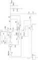
图1是本发明提供的开关型电源控制电路组成示意图;1 is a schematic diagram of the composition of a switching power supply control circuit provided by the present invention;
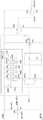
图2是本发明一实施例提供的开关频率控制电路的电路组图;2 is a circuit diagram of a switching frequency control circuit provided by an embodiment of the present invention;
图3是本发明一实施例中PWM时间控制模块组成示意图;3 is a schematic diagram of the composition of a PWM time control module in an embodiment of the present invention;
图4是本发明一实施例的PWM时间控制模块的实施电路图;4 is an implementation circuit diagram of a PWM time control module according to an embodiment of the present invention;
图5是本发明一实施例的输出电压、参考电压及跟随电压波形图;5 is a waveform diagram of an output voltage, a reference voltage and a follower voltage according to an embodiment of the present invention;
图6是本发明一实施例的电感电流及相关PWM信号波形图。FIG. 6 is a waveform diagram of inductor current and related PWM signals according to an embodiment of the present invention.
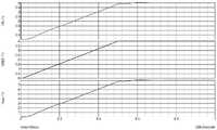
图7是本发明一实施例的主要器件在负载变化时工作波形图;7 is a working waveform diagram of a main device of an embodiment of the present invention when the load changes;
图8是本发明一实施例的主要器件在负载不变时工作波形图。FIG. 8 is a working waveform diagram of the main components of an embodiment of the present invention when the load remains unchanged.
具体实施方式Detailed ways
下面将结合本发明实施例中的附图,对本发明实施例中的技术方案进行清楚、完整地描述,显然,所描述的实施例仅仅是本发明一部分实施例,而不是全部的实施例。基于本发明中的实施例,本领域普通技术人员在没有做出创造性劳动前提下所获得的所有其他实施例,都属于本发明保护的范围。The technical solutions in the embodiments of the present invention will be clearly and completely described below with reference to the accompanying drawings in the embodiments of the present invention. Obviously, the described embodiments are only a part of the embodiments of the present invention, but not all of the embodiments. Based on the embodiments of the present invention, all other embodiments obtained by those of ordinary skill in the art without creative efforts shall fall within the protection scope of the present invention.
本发明的说明书和权利要求书及上述附图中的术语“第一”、“第二”、“第三”“第四”等(如果存在)是用于区别类似的对象,而不必用于描述特定的顺序或先后次序。应该理解这样使用的数据在适当情况下可以互换,以便这里描述的本发明的实施例能够以除了在这里图示或描述的那些以外的顺序实施。此外,术语“包括”和“具有”以及他们的任何变形,意图在于覆盖不排他的包含,例如,包含了一系列步骤或单元的过程、方法、系统、产品或设备不必限于清楚地列出的那些步骤或单元,而是可包括没有清楚地列出的或对于这些过程、方法、产品或设备固有的其它步骤或单元。The terms "first", "second", "third", "fourth", etc. (if present) in the description and claims of the present invention and the above-mentioned drawings are used to distinguish similar objects and are not necessarily used to Describe a particular order or sequence. It is to be understood that the data so used may be interchanged under appropriate circumstances such that the embodiments of the invention described herein can be practiced in sequences other than those illustrated or described herein. Furthermore, the terms "comprising" and "having" and any variations thereof, are intended to cover non-exclusive inclusion, for example, a process, method, system, product or device comprising a series of steps or units is not necessarily limited to those expressly listed Rather, those steps or units may include other steps or units not expressly listed or inherent to these processes, methods, products or devices.
下面以具体地实施例对本发明的技术方案进行详细说明。下面这几个具体的实施例可以相互结合,对于相同或相似的概念或过程可能在某些实施例不再赘述。The technical solutions of the present invention will be described in detail below with specific examples. The following specific embodiments may be combined with each other, and the same or similar concepts or processes may not be repeated in some embodiments.
参考图1所示,本实施例提供了一种开关频率控制电路,包括:开关电源10、PWM控制模块20、开关导通控制模块30以及数字模块40;其中:Referring to FIG. 1, this embodiment provides a switching frequency control circuit, including: a switching power supply 10, a
开关电源10包括第一开关支路11及第二开关支路12,第一开关支路11的第一端连接输入电压端(VIN),其第二端连接第一参考节点X1,第一开关支路11的控制端连接PWM控制模块20的第一端;第二开关支路12的第一端连接第一参考节点X1,其第二端连接接地端(GND),第二开关支路12的控制端连接PWM控制模块20的第二端;第一开关支路11配置为在第一驱动信号(HS)的作用下导通输入电压(VIN)与第一参考节点X1,第二开关支路12配置为在第二驱动信号(LS)的作用下导通第一参考节点X1及接地端(GND);The switching power supply 10 includes a
PWM控制模块20的输入端用于接收PWM脉冲信号,并在PWM脉冲信号的作用下,通过其第一端输出第一驱动信号(HS),通过其第二端输出第二驱动信号(LS);The input end of the
开关导通控制模块30的第一端连接第一参考节点X1,开关导通控制模块30的第二端连接PWM控制模块20的第三端;开关导通控制模块30用于用于采集第一参考节点X1处的电流,当第一参考节点X1处的电流超出预设阈值时通过PWM控制模块20关断第一开关支路11并导通所述第二开关支路12;否则采用第一参考节点X1处的电流调整PWM脉冲信号;及The first end of the switch conduction control module 30 is connected to the first reference node X1, the second end of the switch conduction control module 30 is connected to the third end of the
数字模块40的第一端与PWM控制模块20的第四端连接,用于进行第一驱动信号(HS)及第二驱动信号(LS)的开关频率调整。The first end of the
该开关频率控制电路通过开关导通控制模块30同时采集第一开关支路11及第二开关支路12间的电流。开关导通控制模块30结合峰值电流控制技术,根据采集的电流大小进行PWM控制模块20输出的调整。具体地,在电流超出预设阈值时,关断第一开关支路,打开导通第二开关支路,否则通过PWM控制模块调整所述PWM脉冲信号进而调整第一驱动信号(HS)及第二驱动信号(LS)保障开关电源的正常工作。这种方式保证了环路工作的连续性,同时也通过峰值电流控制摆脱了次谐波震荡的不足。同时,通过数字模块进行开关频率调整,由于开关导通控制模块及PWM控制模块使得该电路的开关电源不需要斜坡补偿,进而使得开关电源的频率调整控制高效稳定,并有利于在此基础上执行频率展宽(SSCG)等频率调制方案。The switching frequency control circuit simultaneously collects the current between the first switching
参考图2所示,本实施例中的开关电源具体配置为包括第一相位功率管M1构成的第一开关支路11及第二相位功率管M2构成的第二开关支路12,其中,输入电压端VIN设置在第一相位功率管M1的输入端处,第一相位功率管M1及第二相位功率管M2间的第一参考节点X1与输出电压端Vout间依次串联有一储能电感L0及采集电阻RS。其中,RLOAD为开关电源的输出负载,这里用来模拟用户端的实际使用情况。当然,在其他优选实施例中,该开关电源可以根据需要变换为其他的具有两个开关支路的电源,其第一参考节点X1与输出电压端Vout间可以仅设置一储能电感或根据需要设置其他种类及数量的储能元件。Referring to FIG. 2 , the switching power supply in this embodiment is specifically configured to include a
参考图2所示,本实施例中的数字模块U9主要用于运算和逻辑控制。具体地,数字模块U9配置为:在(软)启动时候维持系统默认参数;轻载模式下维持之前的(控制)参数数据不变;而在连续模式下,数字模块U9则设置为比较第一驱动信号及第二驱动信号的开关频率和振荡器频率,如果开关频率大于参考频率,则会增大所述PWM脉冲信号的延时,反之降低所述PWM脉冲信号的延时,直到开关频率值在参考频率相近,即开关频率与所述参考频率间的差值小于预设差值。该数字模块U9的设置,可以通过对PWM脉冲信号延时的调节,进而调制PWM控制模块20输出的信号的开关频率变化,实现降低开关电源EMI的目的。Referring to FIG. 2 , the digital module U9 in this embodiment is mainly used for operation and logic control. Specifically, the digital module U9 is configured to: maintain the system default parameters during (soft) startup; keep the previous (control) parameter data unchanged in the light load mode; and in the continuous mode, the digital module U9 is set to compare the first The switching frequency and oscillator frequency of the driving signal and the second driving signal, if the switching frequency is greater than the reference frequency, the delay of the PWM pulse signal will be increased, otherwise the delay of the PWM pulse signal will be reduced until the switching frequency value When the reference frequencies are close, that is, the difference between the switching frequency and the reference frequency is smaller than the preset difference. The setting of the digital module U9 can achieve the purpose of reducing the EMI of the switching power supply by adjusting the delay of the PWM pulse signal, thereby modulating the switching frequency of the signal output by the
参考图2,进一步优选的,还包括参考时钟发生器U10,配置为与数字模块U9的第二端连接,以为数字模块U9产生参考频率的时钟源。本实施例中的参考时钟发生器U10较容易修调和设计。Referring to FIG. 2 , further preferably, a reference clock generator U10 is further included, which is configured to be connected to the second end of the digital module U9 to generate a clock source of reference frequency for the digital module U9. The reference clock generator U10 in this embodiment is easier to tune and design.
进一步优选实施例中,参考图2所示,开关导通控制模块30包括:电流采集电路U6,与开关电源10连接以采集第一参考节点X1处的电流,采集第一参考节点X1的电流后将其处理为便于后续比较处理的拉电流(source电流)并输出。In a further preferred embodiment, as shown in FIG. 2 , the switch conduction control module 30 includes: a current collection circuit U6, which is connected to the switching power supply 10 to collect the current at the first reference node X1, and after collecting the current at the first reference node X1, It is processed as a source current for subsequent comparison processing and output.
进一步地,该开关频率控制电路在配置为还包括串联于第一参考节点X1及输出电压端Vout间的第一电感(即上述的储能电感L0)及第一电阻(即上述的采集电阻RS)。在此情况下,这里的电流采集电路U6的第一端连接在第一电感L0与第一电阻RS之间的节点处,电流采集电路U6的第二端连接在第一电阻RS与输出电压端Vout之间的节点。电流采集电路U6同时采集位于第一电感L0及第一电阻RS间节点处的电流,及第一电阻RS与输出电压间节点处的电流,并将采集的电流分别处理为拉电流后,再分别通过电流采集电路U6的第三端与第四端输出相应的拉电流。具体地,结合图2所示,采集电流后通过预设比例处理为拉电流,然后分别通过U6的OUT1和OUT2端口输出。其中,I(out1)=I(电感)/n(其中n为第一预设比例系数);I(out2)=I(电感)/m(其中m为第二预设比例系数)。Further, the switching frequency control circuit is configured to further include a first inductance (that is, the above-mentioned energy storage inductance L0) and a first resistor (that is, the above-mentioned collection resistor RS) connected in series between the first reference node X1 and the output voltage terminal Vout. ). In this case, the first end of the current collecting circuit U6 is connected at the node between the first inductor L0 and the first resistor RS, and the second end of the current collecting circuit U6 is connected between the first resistor RS and the output voltage end Nodes between Vout. The current collection circuit U6 simultaneously collects the current at the node between the first inductor L0 and the first resistor RS, and the current at the node between the first resistor RS and the output voltage, and processes the collected currents as pulling currents, respectively. The corresponding pull current is output through the third terminal and the fourth terminal of the current collecting circuit U6. Specifically, as shown in FIG. 2 , after the current is collected, it is processed into a current source by a preset ratio, and then output through the OUT1 and OUT2 ports of U6 respectively. Wherein, I(out1)=I(inductance)/n (wherein n is a first preset proportional coefficient); I(out2)=I(inductance)/m (wherein m is a second preset proportionality coefficient).
优选地,开关导通控制模块还包括:过流比较器U4,过流比较器U4的正相输入端与电流采集电路U6的第三端相连,过流比较器U4的负相输入端用于输入与上述预设阈值对应的参考电压;过流比较器U4的输出端与PWM控制模块20的第三端连接。工作时,过流比较器U4用于将电流采集电路U6的第三端输出的拉电流(即OUT2端口输出的I(out2))与预设阈值对应的参考电压进行比较,当电流采集电路U6的第三端输出的拉电流I(out2)大于预设阈值对应的参考电压时,输出关断信号控制PWM控制模块关断第一开关支路并导通第二开关支路。其中,参考图2所示,这里的电流的预设阈值由参考电压(CL2_REF)、第二预设比例系数m及过流比较器的上拉电阻RLIM的阻值共同决定。当发生过流后,输出关断信号立刻关闭PWM(pwm=0),上管(第一相位功率管M1)关断,并切换为下管(第二相位功率管M2)导通,在过流释放之前,不允许上管(第一相位功率管M1)开启导通。当过流释放完成后,过流比较器U4输出ILIM信号可以控制PWM控制模块进行复位使电路的第一开关支路继续工作。Preferably, the switch conduction control module further includes: an overcurrent comparator U4, the positive phase input terminal of the overcurrent comparator U4 is connected to the third terminal of the current acquisition circuit U6, and the negative phase input terminal of the overcurrent comparator U4 is used for The reference voltage corresponding to the above preset threshold is input; the output end of the overcurrent comparator U4 is connected to the third end of the
优选地,该开关频率控制电路还包括:PWM比较器U1,PWM比较器U1的正相输入端用于输入一PWM补偿信号,PWM比较器U1的负相输入端与电流采集电路U6的第四端相连;PWM比较器U1的输出端与PWM控制模块20的输入端相连,用于输出PWM脉冲信号给PWM控制模块20的输入端。工作时,PWM比较器U1将电流采集电路U6的第四端输出的拉电流对应的信号(CS1)与PWM补偿信号(compf)进行比较,以产生PWM脉冲信号(pulse)并发送至上述的PWM控制模块。本实施例中,PWM脉冲信号的上升沿用于产生关断信号(第一相位的结束信号)。Preferably, the switching frequency control circuit further comprises: a PWM comparator U1, the positive phase input terminal of the PWM comparator U1 is used to input a PWM compensation signal, the negative phase input terminal of the PWM comparator U1 is connected to the fourth phase input terminal of the current acquisition circuit U6 The output end of the PWM comparator U1 is connected to the input end of the
进一步地,该开关频率控制电路还包括:补偿网络U3,与PWM比较器U1的正相输入端连接,用于产生PWM补偿信号至PWM比较器U1以产生PWM脉冲信号。Further, the switching frequency control circuit further includes: a compensation network U3, connected to the non-inverting input terminal of the PWM comparator U1, for generating a PWM compensation signal to the PWM comparator U1 to generate a PWM pulse signal.
进一步地,该开关频率控制电路还包括:分压下电阻R4、分压上电阻R5以及运算放大器U5,分压上电阻R5与分压下电阻R4串联连接在输出电压端Vout与地之间;运算放大器U5的正相输入端连接在分压上电阻R5与分压下电阻R4之间的节点,运算放大器U5的负相输入端与运算放大器U5的输出端连接,运算放大器U5的输出端与电流采集电路的第四端连接。运算放大器U5用于接收开关电源的分压后的输出电压Vfb以产生跟随电压Vfb_bf,并叠加作用在电流采集电路U6的第四端输出的拉电流(OUT2端口输出的I(out1))上,得到上述的信号CS1,进而调整生成的PWM脉冲信号。Further, the switching frequency control circuit also includes: a voltage dividing resistor R4, a voltage dividing resistor R5 and an operational amplifier U5, and the voltage dividing resistor R5 and the voltage dividing resistor R4 are connected in series between the output voltage terminal Vout and the ground; The positive-phase input terminal of the operational amplifier U5 is connected to the node between the voltage-dividing upper resistor R5 and the voltage-dividing lower resistor R4, the negative-phase input terminal of the operational amplifier U5 is connected to the output terminal of the operational amplifier U5, and the output terminal of the operational amplifier U5 is connected to the output terminal of the operational amplifier U5. The fourth terminal of the current collecting circuit is connected. The operational amplifier U5 is used to receive the divided output voltage Vfb of the switching power supply to generate the follower voltage Vfb_bf, and superimpose it on the source current output by the fourth terminal of the current collection circuit U6 (I(out1) output by the OUT2 port), The above-mentioned signal CS1 is obtained, and the generated PWM pulse signal is further adjusted.
进一步地,该开关频率控制电路还包括:误差放大器U7,误差放大器U7的正相输入端连接在分压上电阻R5与分压下电阻R4之间的节点,误差放大器U7的负相输入端用于接入一参考目标电压,误差放大器U7的输出端与补偿网络U3的输出端连接。误差放大器U7用于比较开关电源的分压后的输出电压Vfb与参考目标电压VREF间的误差,并进行PWM补偿信号的调整以精确控制开关电源的输出电压。Further, the switching frequency control circuit also includes: an error amplifier U7, the positive-phase input end of the error amplifier U7 is connected to the node between the voltage-dividing upper resistor R5 and the voltage-dividing lower resistor R4, and the negative-phase input end of the error amplifier U7 is used for For connecting to a reference target voltage, the output end of the error amplifier U7 is connected to the output end of the compensation network U3. The error amplifier U7 is used to compare the error between the divided output voltage Vfb of the switching power supply and the reference target voltage VREF, and adjust the PWM compensation signal to precisely control the output voltage of the switching power supply.
参考图2所示,本实施例中的PWM控制模块还包括PWM时间控制模块U2。进一步参考图3所示,PWM时间控制模块U2包括调整PWM脉冲信号导通时间的第一信号产生单元I01、第二信号产生单元I02及第三信号产生单元I03;其中,第一信号产生单元I01配置为接收PWM信号及PWM脉冲信号以产生最小关断时间控制信号;所述第二信号产生单元I02配置为接收所述最小关断时间控制信号并产生最大导通时间控制信号;所述第三信号产生单元I03配置为接收所述最大导通时间控制信号并产生最小导通时间控制信号。PWM时间控制模块U2通过上述的第一信号产生单元I01、第二信号产生单元I02及第三信号产生单元I03进行PWM脉冲信号的最小关断时间、最大导通时间及最小导通时间的控制及调整。为实现上述进行PWM脉冲信号控制及调整的功能,U2内部电路的一个具体实施例可以参考专利CN201711138251.6,或者本领域技术人员根据需要设置为其他可以实现上述功能的具体电路结构。Referring to FIG. 2 , the PWM control module in this embodiment further includes a PWM time control module U2. Further referring to FIG. 3, the PWM time control module U2 includes a first signal generating unit I01, a second signal generating unit I02 and a third signal generating unit I03 for adjusting the on-time of the PWM pulse signal; wherein, the first signal generating unit I01 is configured to receive a PWM signal and a PWM pulse signal to generate a minimum off-time control signal; the second
参考图4所示,U2的一个信号单元实施如虚线框内部分所示,用来配置电流源,其中,电流源和电容共同来确定PWM信号的延时可调过程。电流源作为大小可编程电流源,其控制来自数字处理,较大的电流对于相同的电容,充到相同的翻转电压需要的时间(延时)短,反之长。电流的大小和延时成正比例关系,所以可以通过调整电流源的大小(从0调到最大)来调节延时,对于电容,同理。Referring to FIG. 4 , a signal unit of U2 is implemented as shown in the dashed box, and is used to configure the current source, wherein the current source and the capacitor jointly determine the delay adjustment process of the PWM signal. The current source is used as a programmable current source, and its control comes from digital processing. For the same capacitor with a larger current, the time (delay) required to charge to the same inversion voltage is short, and vice versa. The magnitude of the current is proportional to the delay, so the delay can be adjusted by adjusting the size of the current source (from 0 to the maximum), and the same is true for capacitors.
这里当过流比较器U4控制第一比较支路关断后,且过流释放完成后,过流比较器U4输出ILIM信号可以控制PWM时间控制模块U2进行复位,使其输出复位0,电路的第一开关支路继续工作,进而U2实现了在连续模式下产生第一相位开启信号。Here, after the overcurrent comparator U4 controls the first comparison branch to turn off, and after the overcurrent release is completed, the overcurrent comparator U4 outputs the ILIM signal to control the PWM time control module U2 to reset, so that the output of the circuit is reset to 0. The first switching branch continues to work, and U2 realizes the generation of the first phase turn-on signal in the continuous mode.
进一步优选地,参考图2所示,PWM控制模块还包括开关管驱动单元U8,与PWM时间控制模块U2连接,用于接收PWM时间控制模块U2调整后的PWM脉冲信号,以产生第一驱动信号(HS)及第二驱动信号(LS)。Further preferably, with reference to FIG. 2, the PWM control module also includes a switch tube drive unit U8, which is connected to the PWM time control module U2 and is used to receive the PWM pulse signal adjusted by the PWM time control module U2 to generate the first drive signal. (HS) and the second drive signal (LS).
进一步参考图2,该开关频率控制电路工作过程如下:Further referring to Fig. 2, the working process of the switching frequency control circuit is as follows:
启动时,输出电压端Vout的初始电压为0V,而VREF电压为参考目标电压,通常有软启动,VREF电压缓启动到目标电压,Vfb跟随VREF,直至达到目标电压;Vout=Vfb*(1+R5/R4),其中R4为分压下电阻,R5为分压上电阻。When starting, the initial voltage of the output voltage terminal Vout is 0V, and the VREF voltage is the reference target voltage, usually there is a soft start, the VREF voltage starts slowly to the target voltage, and Vfb follows VREF until it reaches the target voltage; Vout=Vfb*(1+ R5/R4), where R4 is the resistor under the voltage divider, and R5 is the resistor on the voltage divider.
此时,误差放大器U7比较输入端误差,从而抬高或者降低compf电压,这里的补偿网络U3设置为环路滤波器,U7和U3共同决定了环路的速度(带宽)。本实施例中,如Vfb<VREF,U7输出电流抬高compf;如Vfb>VREF,则反之。At this time, the error amplifier U7 compares the error at the input, thereby raising or lowering the compf voltage. The compensation network U3 here is set as a loop filter, and U7 and U3 together determine the speed (bandwidth) of the loop. In this embodiment, if Vfb<VREF, the output current of U7 increases compf; if Vfb>VREF, the opposite is true.
而运算放大器U5执行以下功能:1、复制(缓冲)Vfb电压以提高驱动能力;2.隔离Vfb和Vfb_bf,由于运放的高阻输入特性,Vfb_bf的变化不会影响到Vfb;这里由于U5速度远高于环路带宽,所以Vfb_bf的交流量近似等于Vfb;Vfb_bf跟随Vfb信号变化,即跟随器。在一具体应用例中,输出电压Vout、分压后的Vfb及参考目标电压VREF的变化波形关系参考图5所示。The operational amplifier U5 performs the following functions: 1. Copy (buffer) the Vfb voltage to improve the driving capability; 2. Isolate Vfb and Vfb_bf, due to the high-impedance input characteristic of the operational amplifier, the change of Vfb_bf will not affect Vfb; here due to the speed of U5 Much higher than the loop bandwidth, so the AC amount of Vfb_bf is approximately equal to Vfb; Vfb_bf follows the Vfb signal change, that is, a follower. In a specific application example, the waveform relationship between the output voltage Vout, the divided Vfb and the reference target voltage VREF is shown in FIG. 5 .
该过程中,电流采集电路U6进行电感电流采集,并处理为拉电流后分别输出I(out1)及I(out2)。本实施例中,对于上管,用器件尺寸为M1的1/n的采集管作为镜像管,镜像出来的电流为M1的1/n,下管采集同理。另外,在电感端串联采集电阻RS,其上压降为RS*IL(IL为电感电流,即I(电感)),使该压降落在不同的参考电阻之上就可以转为相应的拉电流,通过设置参考电阻和RS的比例可以得到I(out1)和I(out2)。In this process, the current acquisition circuit U6 collects the inductor current, and processes the current to output I(out1) and I(out2) respectively after processing it to pull the current. In this embodiment, for the upper tube, a collection tube with a device size of 1/n of M1 is used as a mirror tube, and the mirrored current is 1/n of M1, and the same is true for lower tube collection. In addition, a collection resistor RS is connected in series at the inductor end, and the voltage drop on it is RS*IL (IL is the inductor current, that is, I (inductance)), so that the voltage drop above different reference resistors can be converted into the corresponding source current. , I(out1) and I(out2) can be obtained by setting the ratio of the reference resistance and RS.
该过程中,通过过流比较器U4进行逐周期过流保护,过流时上管关断,切换为下管导通,在过流释放之前,不允许上管开启导通;上下管采集到的电流表示为Is=IL/m,当Is*RLIM>CL2_REF,表明电流超过预设,ILIM变为高,上管立刻关断,下管开;反之ILIM为低,环路工作。During this process, cycle-by-cycle overcurrent protection is performed by the overcurrent comparator U4. When overcurrent occurs, the upper tube is turned off and switched to the lower tube conducting. Before the overcurrent is released, the upper tube is not allowed to be turned on and conducting; The current is expressed as Is=IL/m. When Is*RLIM>CL2_REF, it indicates that the current exceeds the preset value, ILIM becomes high, the upper tube is immediately turned off, and the lower tube is turned on; otherwise, ILIM is low, and the loop works.
该过程中,PWM时间控制模块U2进行PWM脉冲信号的最小关断时间、最大导通时间及最小导通时间的控制及调整,同时主要用于在连续模式下产生第一相位开启信号:In this process, the PWM time control module U2 controls and adjusts the minimum off-time, maximum on-time and minimum on-time of the PWM pulse signal, and is mainly used to generate the first phase turn-on signal in continuous mode:
在连续模式下,由于电感电流IL连续,达到峰值电流关闭的时候pulse(图3中输入U2的PU)只有很短的时间维持为低电平(CS1电平由于叠加了电感电流信号,始终大于输入U1的compf电压,这里一实施例中,电感电流I(L1-P)、PWM脉冲信号、compf/CS1信号、pulse信号波形关系参考图6所示),用于关闭第一相位和开启第二相位,由于第二相位的关闭有最小off时间控制,所以在连续模式下等效为恒定关断时间(关断时间为U2-I02模块的最小off时间);In continuous mode, since the inductor current IL is continuous, when the peak current is turned off, the pulse (PU input to U2 in Figure 3) only remains at a low level for a short time (the CS1 level is always greater than Input the compf voltage of U1. In this embodiment, the relationship between the inductor current I (L1-P), the PWM pulse signal, the compf/CS1 signal, and the pulse signal waveform relationship is shown in Figure 6), which is used to turn off the first phase and turn on the first phase. Two-phase, since the closing of the second phase is controlled by the minimum off time, it is equivalent to a constant off time in continuous mode (the off time is the minimum off time of the U2-I02 module);
在断续模式下,处于工作与导通时间控制模式,导通时间受控于U2模块的I02/I03控制叠加电感电流并主要受控于电感电流叠加与RLIM上的电压控制。由于电感叠加量无论在断续模式还是连续模式,都主要受控于电感电流,所以稳定性模型与峰值电流结构近似,因此环路补偿比较简单。In the discontinuous mode, it is in the working and on-time control mode, and the on-time is controlled by the I02/I03 of the U2 module to control the superimposed inductor current and is mainly controlled by the superposition of the inductor current and the voltage control on the RLIM. Since the inductance superposition is mainly controlled by the inductor current in both discontinuous mode and continuous mode, the stability model is similar to the peak current structure, so the loop compensation is relatively simple.
参考图7所示,在负载变化时,软启动(软启动结束信号SSDONE变1之前),sel<4:0>维持默认值10000(这里的sel<4:0>为数字输出,其值和电流大小成对应关系,用来决定延时大小。);轻载(PFM=1),sel维持原来的值不变化;退出两者模式后,sel开始调整;直到最后频率值和设定值接近或相等,或者到了调制的最大范围后停止。Referring to Figure 7, when the load changes, soft start (before the soft start end signal SSDONE becomes 1), sel<4:0> maintains the default value of 10000 (here sel<4:0> is a digital output, and its value and The magnitude of the current has a corresponding relationship, which is used to determine the size of the delay.); light load (PFM=1), sel maintains the original value; after exiting the two modes, sel starts to adjust; until the final frequency value is close to the set value or equal, or stop after reaching the maximum range of modulation.
参考图8所示,在负载不变时,启动电路,频率最后固定在360khz。TOFF关断时间在间歇调整。Referring to Figure 8, when the load remains unchanged, the circuit is started, and the frequency is finally fixed at 360khz. TOFF off time is adjusted intermittently.
该开关频率控制电路由于设置了PWM时间控制模块U2,因此不需要在burst模式(轻载)切换,工作频率,占空比均会自动调整;另外,由于未限定固定开关周期,所以电感电流的抖动不会被放大,从而导致次谐波震荡,所以在无斜坡补偿的情况下,环路也很稳定,可以很好的提高抗噪声能力。Since the PWM time control module U2 is set in the switching frequency control circuit, it does not need to switch in burst mode (light load), and the operating frequency and duty cycle will be automatically adjusted; in addition, since the fixed switching period is not defined, the inductor current The jitter will not be amplified, resulting in sub-harmonic oscillation, so the loop is also very stable without slope compensation, which can improve the noise immunity.
综上所述,本发明提供的开关频率控制电路,通过开关导通(TON)控制模块控制PWM时间控制模块U2并结合峰值电流控制,摆脱了次谐波震荡的不足。其中,第一开关支路电流作为导通时间控制,与传统峰值电流控制相似,环路补偿方式易实现。在此基础上,通过数字模块控制PWM时间控制模块U2进行频率控制,这种频率控制的方式简单高效,非常适合工业大规模量产。To sum up, in the switching frequency control circuit provided by the present invention, the PWM time control module U2 is controlled by the on-off (TON) control module and combined with the peak current control, so as to get rid of the deficiency of sub-harmonic oscillation. Among them, the first switch branch current is used as the on-time control, which is similar to the traditional peak current control, and the loop compensation method is easy to realize. On this basis, the digital module controls the PWM time control module U2 for frequency control. This frequency control method is simple and efficient, and is very suitable for industrial mass production.
本发明使用的是数字为主的方案,借助于混合电流模+时间控制结构,使得通过调整TOFF时间即可完成开关频率的调整,通过数字模块执行运算和逻辑控制进而完成数字控制,稳定性极佳,而且由于采用了数字方案,还很容易实现展频等功能。The present invention uses a digital-based scheme, with the help of the hybrid current mode + time control structure, so that the adjustment of the switching frequency can be completed by adjusting the TOFF time, and the digital control can be completed by performing operations and logic control through the digital module, and the stability is extremely high. It is good, and because of the digital scheme, it is easy to realize functions such as spread spectrum.
此外,该开关频率控制电路通过运算放大器U5实现Vfb缓冲,隔离了电感电流IL对Vfb的影响,同时提高了电路结构的适用范围(由于Vfb经过了电阻的分压,无驱动能力)。如果没有U5的存在,此架构只能够通过VOUT直接反馈(Vout有大电容和驱动能力),无法经过电阻分压后直接叠加电感电流分量。In addition, the switching frequency control circuit realizes Vfb buffering through the operational amplifier U5, which isolates the influence of the inductor current IL on Vfb, and at the same time improves the applicable range of the circuit structure (because Vfb is divided by resistors, it has no driving ability). If there is no U5, this architecture can only directly feedback through VOUT (Vout has a large capacitance and driving ability), and cannot directly superimpose the inductor current component after the resistor divider.
由于交流反馈量为电感电流,可以降低对Vout端电容COUT的电容寄生等效电阻ESR的依赖性,进而降低Vout电压纹波。Since the AC feedback amount is the inductor current, the dependence on the capacitance parasitic equivalent resistance ESR of the capacitor COUT at the Vout terminal can be reduced, thereby reducing the Vout voltage ripple.
最后应说明的是:以上各实施例仅用以说明本发明的技术方案,而非对其限制;尽管参照前述各实施例对本发明进行了详细的说明,本领域的普通技术人员应当理解:其依然可以对前述各实施例所记载的技术方案进行修改,或者对其中部分或者全部技术特征进行等同替换;而这些修改或者替换,并不使相应技术方案的本质脱离本发明各实施例技术方案的范围。Finally, it should be noted that the above embodiments are only used to illustrate the technical solutions of the present invention, but not to limit them; although the present invention has been described in detail with reference to the foregoing embodiments, those of ordinary skill in the art should understand that: The technical solutions described in the foregoing embodiments can still be modified, or some or all of the technical features thereof can be equivalently replaced; and these modifications or replacements do not make the essence of the corresponding technical solutions deviate from the technical solutions of the embodiments of the present invention. scope.
Claims (12)
Priority Applications (1)
| Application Number | Priority Date | Filing Date | Title |
|---|---|---|---|
| CN202210550083.6ACN114977792A (en) | 2022-05-20 | 2022-05-20 | Switching Frequency Control Circuit |
Applications Claiming Priority (1)
| Application Number | Priority Date | Filing Date | Title |
|---|---|---|---|
| CN202210550083.6ACN114977792A (en) | 2022-05-20 | 2022-05-20 | Switching Frequency Control Circuit |
Publications (1)
| Publication Number | Publication Date |
|---|---|
| CN114977792Atrue CN114977792A (en) | 2022-08-30 |
Family
ID=82984851
Family Applications (1)
| Application Number | Title | Priority Date | Filing Date |
|---|---|---|---|
| CN202210550083.6APendingCN114977792A (en) | 2022-05-20 | 2022-05-20 | Switching Frequency Control Circuit |
Country Status (1)
| Country | Link |
|---|---|
| CN (1) | CN114977792A (en) |
Cited By (1)
| Publication number | Priority date | Publication date | Assignee | Title |
|---|---|---|---|---|
| CN118170239A (en)* | 2024-03-14 | 2024-06-11 | 深圳市浩海视讯科技有限公司 | Intelligent energy-saving circuit of video main board and control method |
Citations (5)
| Publication number | Priority date | Publication date | Assignee | Title |
|---|---|---|---|---|
| US7145317B1 (en)* | 2004-12-13 | 2006-12-05 | Intersil Americas Inc. | Constant frequency duty cycle independent synthetic ripple regulator |
| CN103532384A (en)* | 2012-11-02 | 2014-01-22 | 成都芯源系统有限公司 | Switch mode power supply and frequency control method and control circuit thereof |
| CN105337496A (en)* | 2014-05-29 | 2016-02-17 | 展讯通信(上海)有限公司 | Pulse frequency modulation circuit based on voltage controlled oscillator |
| CN107947574A (en)* | 2017-11-16 | 2018-04-20 | 上海芯导电子科技有限公司 | A kind of DC DC Switching Power Supplies for improving control model |
| CN109149938A (en)* | 2018-08-30 | 2019-01-04 | 上海芯导电子科技有限公司 | A kind of DC-DC circuit |
- 2022
- 2022-05-20CNCN202210550083.6Apatent/CN114977792A/enactivePending
Patent Citations (5)
| Publication number | Priority date | Publication date | Assignee | Title |
|---|---|---|---|---|
| US7145317B1 (en)* | 2004-12-13 | 2006-12-05 | Intersil Americas Inc. | Constant frequency duty cycle independent synthetic ripple regulator |
| CN103532384A (en)* | 2012-11-02 | 2014-01-22 | 成都芯源系统有限公司 | Switch mode power supply and frequency control method and control circuit thereof |
| CN105337496A (en)* | 2014-05-29 | 2016-02-17 | 展讯通信(上海)有限公司 | Pulse frequency modulation circuit based on voltage controlled oscillator |
| CN107947574A (en)* | 2017-11-16 | 2018-04-20 | 上海芯导电子科技有限公司 | A kind of DC DC Switching Power Supplies for improving control model |
| CN109149938A (en)* | 2018-08-30 | 2019-01-04 | 上海芯导电子科技有限公司 | A kind of DC-DC circuit |
Cited By (2)
| Publication number | Priority date | Publication date | Assignee | Title |
|---|---|---|---|---|
| CN118170239A (en)* | 2024-03-14 | 2024-06-11 | 深圳市浩海视讯科技有限公司 | Intelligent energy-saving circuit of video main board and control method |
| CN118170239B (en)* | 2024-03-14 | 2025-06-13 | 深圳市浩海视讯科技有限公司 | A video mainboard intelligent energy-saving circuit and control method |
Similar Documents
| Publication | Publication Date | Title |
|---|---|---|
| CN109586565B (en) | COT controlled multiphase direct current converter, control circuit and current sharing method | |
| TWI622260B (en) | Buck-boost converter with slope compensation, controller and control method thereof | |
| TWI479787B (en) | Method and apparatus for controlling a conversion of power, and switching regulator | |
| CN105978337B (en) | A kind of offset voltage based on COT control models eliminates circuit | |
| CN106063103B (en) | Burst Mode Control | |
| US8174250B2 (en) | Fixed frequency ripple regulator | |
| CN107104595A (en) | The self-adaptable slop compensation circuit of buck converter is controlled suitable for Peak Current Mode | |
| CN103051220B (en) | Switching Power Supply and controller thereof | |
| CN107147292A (en) | A buck converter with controlled on-time | |
| CN104283430B (en) | Soft start switching power supply conversion device | |
| CN209913707U (en) | Self-adaptive turn-off time timer with adjustable switching frequency | |
| CN105356746A (en) | Conduction time generation circuit for power supply converter, and power supply converter | |
| CN103346663A (en) | Hysteresis control method of Boost convertor | |
| CN114094999A (en) | Converter circuit, corresponding device and method | |
| CN114696615A (en) | Power converter and control circuit thereof | |
| CN114944748B (en) | Constant frequency control circuit and method for constant on-time control mode converter | |
| CN106026650B (en) | A kind of offset voltage eliminates circuit | |
| CN116317558A (en) | Self-adaptive slope compensation peak current control circuit, method and DC-DC converter | |
| CN114977792A (en) | Switching Frequency Control Circuit | |
| CN115459558A (en) | Control circuit and control method of multiphase power conversion circuit and multiphase power supply | |
| CN109980935A (en) | Self-adaptive turn-off time timer with adjustable switching frequency | |
| CN104980023A (en) | Output voltage controlling circuit and power supply provided with same | |
| Adragna et al. | Cycle-by-cycle average input current control of resonant converters | |
| CN114389451A (en) | Switch converter and control circuit and control method thereof | |
| TWM653794U (en) | Power converter circuit and control circuit thereof |
Legal Events
| Date | Code | Title | Description |
|---|---|---|---|
| PB01 | Publication | ||
| PB01 | Publication | ||
| SE01 | Entry into force of request for substantive examination | ||
| SE01 | Entry into force of request for substantive examination |