CN114974339A - Memory array - Google Patents
Memory arrayDownload PDFInfo
- Publication number
- CN114974339A CN114974339ACN202110198021.9ACN202110198021ACN114974339ACN 114974339 ACN114974339 ACN 114974339ACN 202110198021 ACN202110198021 ACN 202110198021ACN 114974339 ACN114974339 ACN 114974339A
- Authority
- CN
- China
- Prior art keywords
- memory array
- magnetic storage
- source line
- extending along
- dummy
- Prior art date
- Legal status (The legal status is an assumption and is not a legal conclusion. Google has not performed a legal analysis and makes no representation as to the accuracy of the status listed.)
- Granted
Links
Images


Classifications
- H—ELECTRICITY
- H10—SEMICONDUCTOR DEVICES; ELECTRIC SOLID-STATE DEVICES NOT OTHERWISE PROVIDED FOR
- H10B—ELECTRONIC MEMORY DEVICES
- H10B61/00—Magnetic memory devices, e.g. magnetoresistive RAM [MRAM] devices
- H10B61/20—Magnetic memory devices, e.g. magnetoresistive RAM [MRAM] devices comprising components having three or more electrodes, e.g. transistors
- H10B61/22—Magnetic memory devices, e.g. magnetoresistive RAM [MRAM] devices comprising components having three or more electrodes, e.g. transistors of the field-effect transistor [FET] type
- G—PHYSICS
- G11—INFORMATION STORAGE
- G11C—STATIC STORES
- G11C11/00—Digital stores characterised by the use of particular electric or magnetic storage elements; Storage elements therefor
- G11C11/02—Digital stores characterised by the use of particular electric or magnetic storage elements; Storage elements therefor using magnetic elements
- G11C11/16—Digital stores characterised by the use of particular electric or magnetic storage elements; Storage elements therefor using magnetic elements using elements in which the storage effect is based on magnetic spin effect
- G11C11/161—Digital stores characterised by the use of particular electric or magnetic storage elements; Storage elements therefor using magnetic elements using elements in which the storage effect is based on magnetic spin effect details concerning the memory cell structure, e.g. the layers of the ferromagnetic memory cell
- G—PHYSICS
- G11—INFORMATION STORAGE
- G11C—STATIC STORES
- G11C11/00—Digital stores characterised by the use of particular electric or magnetic storage elements; Storage elements therefor
- G11C11/02—Digital stores characterised by the use of particular electric or magnetic storage elements; Storage elements therefor using magnetic elements
- G11C11/06—Digital stores characterised by the use of particular electric or magnetic storage elements; Storage elements therefor using magnetic elements using single-aperture storage elements, e.g. ring core; using multi-aperture plates in which each individual aperture forms a storage element
- G11C11/06007—Digital stores characterised by the use of particular electric or magnetic storage elements; Storage elements therefor using magnetic elements using single-aperture storage elements, e.g. ring core; using multi-aperture plates in which each individual aperture forms a storage element using a single aperture or single magnetic closed circuit
- G11C11/06078—Digital stores characterised by the use of particular electric or magnetic storage elements; Storage elements therefor using magnetic elements using single-aperture storage elements, e.g. ring core; using multi-aperture plates in which each individual aperture forms a storage element using a single aperture or single magnetic closed circuit using two or more such elements per bit
- G—PHYSICS
- G11—INFORMATION STORAGE
- G11C—STATIC STORES
- G11C11/00—Digital stores characterised by the use of particular electric or magnetic storage elements; Storage elements therefor
- G11C11/02—Digital stores characterised by the use of particular electric or magnetic storage elements; Storage elements therefor using magnetic elements
- G11C11/14—Digital stores characterised by the use of particular electric or magnetic storage elements; Storage elements therefor using magnetic elements using thin-film elements
- G11C11/15—Digital stores characterised by the use of particular electric or magnetic storage elements; Storage elements therefor using magnetic elements using thin-film elements using multiple magnetic layers
- G—PHYSICS
- G11—INFORMATION STORAGE
- G11C—STATIC STORES
- G11C8/00—Arrangements for selecting an address in a digital store
- G11C8/14—Word line organisation; Word line lay-out
- H—ELECTRICITY
- H10—SEMICONDUCTOR DEVICES; ELECTRIC SOLID-STATE DEVICES NOT OTHERWISE PROVIDED FOR
- H10N—ELECTRIC SOLID-STATE DEVICES NOT OTHERWISE PROVIDED FOR
- H10N50/00—Galvanomagnetic devices
- H10N50/80—Constructional details
Landscapes
- Engineering & Computer Science (AREA)
- Computer Hardware Design (AREA)
- Microelectronics & Electronic Packaging (AREA)
- Semiconductor Memories (AREA)
Abstract
Translated fromChinese
Description
Translated fromChinese技术领域technical field
本发明涉及一种制作半导体元件,尤其是涉及一种高密度磁阻式随机存取存储器(magnetoresistive random access memory,MRAM)阵列。The present invention relates to a manufacturing semiconductor element, in particular to a high-density magnetoresistive random access memory (magnetoresistive random access memory, MRAM) array.
背景技术Background technique
已知,磁阻(magnetoresistance,MR)效应是材料的电阻随着外加磁场的变化而改变的效应,其物理量的定义,是在有无磁场下的电阻差除上原先电阻,用以代表电阻变化率。目前,磁阻效应已被成功地运用在硬盘生产上,具有重要的商业应用价值。此外,利用巨磁阻(GMR)物质在不同的磁化状态下具有不同电阻值的特点,还可以制成磁性随机存储器(MRAM),其优点是在不通电的情况下可以继续保留存储的数据。It is known that the magnetoresistance (MR) effect is the effect that the resistance of the material changes with the change of the external magnetic field. Rate. At present, the magnetoresistance effect has been successfully used in the production of hard disks and has important commercial application value. In addition, using the characteristics of giant magnetoresistance (GMR) substances with different resistance values in different magnetization states, magnetic random access memory (MRAM) can also be made, which has the advantage of continuing to retain stored data without power.
上述磁阻效应还被应用在磁场感测(magnetic field sensor)领域,例如,移动电话中搭配全球定位系统(global positioning system,GPS)的电子罗盘(electroniccompass)零组件,用来提供使用者移动方位等信息。目前,市场上已有各式的磁场感测技术,例如,各向异性磁阻(anisotropic magnetoresistance,AMR)感测元件、GMR感测元件、磁隧穿结(magnetic tunneling junction,MTJ)感测元件等等。然而,上述现有技术的缺点通常包含:较占芯片面积、制作工艺较昂贵、较耗电、灵敏度不足,以及易受温度变化影响等等,而有必要进一步改进。The above-mentioned magnetoresistive effect is also applied in the field of magnetic field sensor, for example, an electronic compass (electronic compass) component in a mobile phone equipped with a global positioning system (GPS) is used to provide the user's moving position and other information. Currently, there are various magnetic field sensing technologies on the market, such as anisotropic magnetoresistance (AMR) sensing elements, GMR sensing elements, and magnetic tunneling junction (MTJ) sensing elements and many more. However, the disadvantages of the above-mentioned prior art generally include: occupying a larger chip area, more expensive manufacturing process, more power consumption, insufficient sensitivity, and being easily affected by temperature changes, etc., and further improvement is necessary.
发明内容SUMMARY OF THE INVENTION
本发明的主要目的在于提供一种高密度磁阻式随机存取存储器(MRAM)阵列,以解决上述现有技术的不足和缺点。The main purpose of the present invention is to provide a high-density magnetoresistive random access memory (MRAM) array to solve the above-mentioned deficiencies and shortcomings of the prior art.
本发明一方面提供一种存储器阵列,包含至少一带区域,包含多个源极线带和多个字线带;至少两个子阵列,包含多个交错的主动磁存储元件,其中,所述至少两个子阵列被所述带区域分开;以及多个交错的虚设磁存储元件,设置在所述带区域内。One aspect of the present invention provides a memory array, comprising at least one region, including a plurality of source line strips and a plurality of word line strips; at least two sub-arrays, including a plurality of interleaved active magnetic storage elements, wherein the at least two sub-arrays are separated by the strip area; and a plurality of interleaved dummy magnetic storage elements disposed within the strip area.
根据本发明实施例,所述多个交错的主动磁存储元件和所述多个交错的虚设磁存储元件被均匀地分布在所述至少两个子阵列和所述带区域上。According to an embodiment of the present invention, the plurality of interleaved active magnetic storage elements and the plurality of interleaved dummy magnetic storage elements are uniformly distributed over the at least two sub-arrays and the strip area.
根据本发明实施例,所述多个交错的虚设磁存储元件包含虚设磁隧穿结(MTJ)元件。According to an embodiment of the invention, the plurality of interleaved dummy magnetic storage elements comprise dummy magnetic tunnel junction (MTJ) elements.
根据本发明实施例,所述虚设MTJ元件的底电极不电连接到所述多个源极线带或所述多个字线带。According to an embodiment of the present invention, the bottom electrodes of the dummy MTJ elements are not electrically connected to the plurality of source line strips or the plurality of word line strips.
根据本发明实施例,所述多个源极线带包含沿着一第一方向延伸的多个第一源极线带和沿着所述第一方向延伸的多个第二源极线带。According to an embodiment of the present invention, the plurality of source line strips include a plurality of first source line strips extending along a first direction and a plurality of second source line strips extending along the first direction.
根据本发明实施例,沿着所述第一方向延伸的所述多个第一源极线带和沿着所述第一方向延伸的所述多个第二源极线带包夹沿着所述第一方向延伸的所述多个字线带。According to an embodiment of the present invention, the plurality of first source line strips extending along the first direction and the plurality of second source line strips extending along the first direction are sandwiched along the the plurality of word line strips extending in the first direction.
根据本发明实施例,各所述多个第一源极线带被连接到沿着一第二方向延伸的一共用源极线。According to an embodiment of the present invention, each of the plurality of first source line strips is connected to a common source line extending along a second direction.
根据本发明实施例,所述第一方向与所述第二方向正交。According to an embodiment of the present invention, the first direction is orthogonal to the second direction.
根据本发明实施例,所述存储器阵列进一步包含沿着所述第一方向延伸且在所述多个第一源极线带正下方的一第一虚设扩散区。According to an embodiment of the present invention, the memory array further includes a first dummy diffusion region extending along the first direction and directly below the plurality of first source line strips.
根据本发明实施例,所述存储器阵列进一步包含沿着所述第一方向延伸且在所述多个第二源极线带正下方的一第二虚设扩散区。According to an embodiment of the present invention, the memory array further includes a second dummy diffusion region extending along the first direction and directly below the plurality of second source line strips.
根据本发明实施例,在所述第一虚设扩散区和所述第二虚设扩散区之间未设置扩散区。According to the embodiment of the present invention, no diffusion region is provided between the first dummy diffusion region and the second dummy diffusion region.
根据本发明实施例,各所述多个交错的主动磁存储元件通过一钨通孔电连接到一存储节点接垫。According to an embodiment of the present invention, each of the plurality of interleaved active magnetic storage elements is electrically connected to a storage node pad through a tungsten via.
根据本发明实施例,在所述带区域内没有布置钨通孔。According to an embodiment of the present invention, no tungsten vias are arranged in the strip region.
根据本发明实施例,所述存储器阵列另包含沿着所述第二方向延伸的多条栅极线。According to an embodiment of the present invention, the memory array further includes a plurality of gate lines extending along the second direction.
根据本发明实施例,所述多个交错的主动磁存储元件包含布置在一第一列中的多个第一主动磁存储元件和布置在一第二列中的多个第二主动磁存储元件,其中,布置在所述第一列中的所述多个第一主动磁存储元件和布置在所述第二列中的所述多个第二主动磁存储元件分别与沿着所述第二方向延伸的所述多条栅极线对准。According to an embodiment of the invention, the plurality of interleaved active magnetic storage elements includes a plurality of first active magnetic storage elements arranged in a first column and a plurality of second active magnetic storage elements arranged in a second column , wherein the plurality of first active magnetic storage elements arranged in the first column and the plurality of second active magnetic storage elements arranged in the second column are The plurality of gate lines extending in the direction are aligned.
附图说明Description of drawings
图1为本发明实施例所绘示的存储器阵列示意图,其中主要显示出主动区域、多晶硅栅极线、位于M1金属层的共用源极线、源极线带和字线带;1 is a schematic diagram of a memory array according to an embodiment of the present invention, which mainly shows an active region, a polysilicon gate line, a common source line located in the M1 metal layer, a source line strip and a word line strip;
图2为本发明实施例所绘示的存储器阵列示意图,其中主要显示出导电通孔、存储节点接垫和钨通孔的位置;2 is a schematic diagram of a memory array according to an embodiment of the present invention, wherein the positions of conductive vias, storage node pads and tungsten vias are mainly shown;
图3为本发明实施例所绘示的存储器阵列示意图,其中主要显示出磁存储元件的位置;3 is a schematic diagram of a memory array according to an embodiment of the present invention, wherein the positions of magnetic storage elements are mainly shown;
图4为本发明实施例所绘示的存储器阵列示意图,其中主要显示出带区域中的V2导电通孔的位置;4 is a schematic diagram of a memory array according to an embodiment of the present invention, wherein the positions of the V2 conductive vias in the band area are mainly shown;
图5为本发明实施例所绘示的存储器阵列示意图,其中主要显示出带区域中的位于M3金属层的接垫的位置;5 is a schematic diagram of a memory array according to an embodiment of the present invention, which mainly shows the position of the pad located in the M3 metal layer in the belt area;
图6为沿着图5中切线I-I’所示的剖面示意图;Figure 6 is a schematic cross-sectional view along the tangent line I-I' shown in Figure 5;
图7为本发明实施例所绘示的存储器阵列示意图,其中主要显示出V3导电通孔的布局;7 is a schematic diagram of a memory array according to an embodiment of the present invention, which mainly shows the layout of the V3 conductive vias;
图8为本发明实施例所绘示的存储器阵列示意图,其中主要显示出M4金属层的布局;8 is a schematic diagram of a memory array according to an embodiment of the present invention, wherein the layout of the M4 metal layer is mainly shown;
图9为本发明实施例所绘示的存储器阵列示意图,其中主要显示出V4导电通孔的布局;9 is a schematic diagram of a memory array according to an embodiment of the present invention, which mainly shows the layout of the V4 conductive via;
图10为本发明实施例所绘示的存储器阵列示意图,其中主要显示出M5金属层的布局;10 is a schematic diagram of a memory array according to an embodiment of the present invention, wherein the layout of the M5 metal layer is mainly shown;
图11为本发明实施例所绘示的存储器阵列的子阵列中的部分结构立体示意图;FIG. 11 is a schematic perspective view of a partial structure of a sub-array of a memory array according to an embodiment of the present invention;
图12为本发明实施例所绘示的存储器阵列的子阵列和带区域中的部分结构立体示意图。FIG. 12 is a schematic perspective view of a partial structure of a sub-array and a strip area of a memory array according to an embodiment of the present invention.
主要元件符号说明Description of main component symbols
1 存储器阵列1 Memory array
100 半导体基底100 Semiconductor substrates
140 钨通孔140 tungsten through hole
210~260 介电层210~260 Dielectric layer
AA 主动区域AA active area
AAd1 第一虚设扩散区AAd1 first dummy diffusion region
AAd2 第二虚设扩散区AAd2 Second Dummy Diffusion Region
BE 下电极BE lower electrode
BL 位线BL bit line
CD 漏极接触差塞CD drain contact differential plug
CP 接触插塞CP contact plug
CS 源极接触差塞CS source contact differential plug
CSL 共用源极线CSL common source line
D1 第一方向D1 first direction
D2 第二方向D2 second direction
DD 漏极区域DD drain region
GL 多晶硅栅极线GL Polysilicon Gate Line
M1~M5 金属层M1~M5 metal layer
MA 主动(有源)磁存储元件MA active (active) magnetic memory element
MA1 第一主动磁存储元件MA1 first active magnetic memory element
MA2 第二主动磁存储元件MA2 second active magnetic memory element
MD 虚设磁存储元件MDdummy magnetic storage element
MAS 子阵列MAS subarray
P1 接垫P1 pad
P2 存储节点接垫P2 storage node pads
PS1、PS2、PW 接垫PS1 , PS2 , PW pads
PVS1、PVS2、PVW 接垫PVS1 , PVS2 , PVW pads
PDS41、PDS42、PDW4 接垫PDS41 , PDS42 , PDW4 pads
SD 源极区域SD source area
SL 源极线SL source line
SLS 源极线带SLS source line strip
SLS1 第一源极线带SLS1 first source line strip
SLS2 第二源极线带SLS2 Second Source Line Strip
SR 带区域SR band area
STI 浅沟绝缘区域STI Shallow Trench Insulation Region
T 晶体管T transistor
TE 上电极TE top electrode
V1~V4 导电通孔V1~V4 Conductive Vias
VA1、VA3 导电通孔VA1 , VA3 conductive vias
VS1、VS2、VW 导电通孔VS1 , VS2 , VW conductive vias
VPS1、VPS2、VPW 导电通孔VPS1 , VPS2 , VPW conductive vias
VDS31、VDS32、VDW3 导电通孔VDS31 , VDS32 , VDW3 conductive vias
VDS41、VDS42、VDW4 导电通孔VDS41 , VDS42 , VDW4 conductive vias
WL 字线WL word line
WLS 字线带WLS word line strip
具体实施方式Detailed ways
在下文中,将参照附图说明细节,该些附图中的内容也构成说明书细节描述的一部分,并且以可实行该实施例的特例描述方式来绘示。下文实施例已描述足够的细节使该领域的一般技术人士得以具以实施。In the following, details will be explained with reference to the accompanying drawings, the contents of which also form a part of the detailed description of the specification, and are shown in a description of a specific example in which this embodiment can be carried out. The following examples are described in sufficient detail to enable those of ordinary skill in the art to practice.
当然,也可采行其他的实施例,或是在不悖离文中所述实施例的前提下作出任何结构性、逻辑性、及电性上的改变。因此,下文得细节描述不应被视为是限制,反之,其中所包含的实施例将由随附的权利要求来加以界定。Of course, other embodiments can also be adopted, or any structural, logical, and electrical changes can be made without departing from the embodiments described herein. Therefore, the following detailed description is not to be regarded as limiting, but rather the embodiments contained therein are to be defined by the appended claims.
本发明披露一种高密度存储器布局,特别是一种高密度磁阻式随机存取存储器(magnetoresistive random access memory,MRAM)阵列,其具体技术特征在于:在两个子阵列(sub-array)之间的一带区域(strap region)内设置多个交错的虚设(dummy)磁存储元件,使得存储器阵列的主动(active)磁存储元件和虚设磁存储元件以交错(staggered)排列方式均匀的分布在两个子阵列和带区域上,实现高密度存储器布局。The present invention discloses a high-density memory layout, especially a high-density magnetoresistive random access memory (MRAM) array, and its specific technical feature is: between two sub-arrays (sub-array) A plurality of staggered dummy magnetic storage elements are arranged in the strap region of the memory array, so that the active magnetic storage elements and dummy magnetic storage elements of the memory array are evenly distributed in the two sub-elements in a staggered arrangement. On the array and strip area, a high-density memory layout is achieved.
在以下详细说明中,以Mn表示金属内连线结构中的不同金属层,其中n为正整数,例如,M1代表金属内连线结构中的第一层金属层,M2代表金属内连线结构中的第二层金属层,以此类推,并以Vn表示金属内连线结构中的不同导电通孔,例如,V1代表连接M1至M2的导电通孔,V2代表连接M2至M3的导电通孔,以此类推。In the following detailed description, Mn represents different metal layers in the metal interconnect structure, where n is a positive integer, for example, M1 represents the first metal layer in the metal interconnect structure, and M2 represents the metal interconnect structure. The second metal layer in , and so on, and Vn represents the different conductive vias in the metal interconnect structure, for example, V1 represents the conductive via connecting M1 to M2, V2 represents the conductive via connecting M2 to M3 holes, and so on.
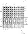
请参阅图1,其为依据本发明实施例所绘示的存储器阵列示意图,其中主要显示出主动区域、多晶硅栅极线、位于M1金属层的共用源极线(common source line)、源极线带(source line strap)和字线带(word line strap)。如图1所示,存储器阵列1包含至少两个子阵列MAS和至少一带区域SR。根据本发明实施例,带区域SR是一个沿着一第一方向D1伸的带状区域,而两个子阵列MAS被带区域SR分开。根据本发明实施例,存储器阵列1另包含多条沿着一第二方向D2延伸的多晶硅栅极线GL和形成在一半导体基底100中的多条沿着第一方向D1延伸的主动区域AA。根据本发明实施例,第一方向D1与第二方向D2正交。根据本发明实施例,主动区域AA彼此被浅沟绝缘区域STI彼此隔离。Please refer to FIG. 1 , which is a schematic diagram of a memory array according to an embodiment of the present invention, which mainly shows an active region, a polysilicon gate line, a common source line located in the M1 metal layer, and a source line Strap (source line strap) and word line strap (word line strap). As shown in FIG. 1 , the memory array 1 includes at least two sub-arrays MAS and at least one band area SR. According to an embodiment of the present invention, the band region SR is a band-shaped region extending along a first direction D1, and the two sub-arrays MAS are separated by the band region SR. According to an embodiment of the present invention, the memory array 1 further includes a plurality of polysilicon gate lines GL extending along a second direction D2 and a plurality of active areas AA extending along the first direction D1 formed in a
根据本发明实施例,多晶硅栅极线GL通过两个子阵列MAS和带区域SR,在子阵列MAS中和主动区域AA交错处构成晶体管T。根据本发明实施例,晶体管T包含一源极区域SD和一漏极区域DD,例如,N+掺杂区,但不限于此。根据本发明实施例,在带区域SR内另设置有分别紧邻于两个子阵列MAS的两条沿着第一方向D1延伸的第一虚设扩散区AAd1和第二虚设扩散区AAd2。根据本发明实施例,第一虚设扩散区AAd1和第二虚设扩散区AAd2可以帮忙提高位于子阵列MAS的边缘的存储器单元的良率。According to the embodiment of the present invention, the polysilicon gate line GL passes through the two sub-arrays MAS and the strip region SR, and forms the transistor T in the sub-array MAS where the active region AA intersects. According to an embodiment of the present invention, the transistor T includes a source region SD and a drain region DD, eg, N+ doped regions, but not limited thereto. According to the embodiment of the present invention, two first dummy diffusion areas AAd1 and second dummy diffusion areas AAd2 extending along the first direction D1 and adjacent to the two sub-arrays MAS are further disposed in the band region SR. According to the embodiment of the present invention, the first dummy diffusion area AAd1 and the second dummy diffusion area AAd2 can help improve the yield of the memory cells located at the edge of the sub-array MAS.
根据本发明实施例,在带区域SR内另设置有位于M1金属层的多个源极线带SLS和多个字线带WLS,其中多个源极线带SLS包含沿着第一方向D1延伸的多个第一源极线带SLS1和沿着第一方向D1延伸的多个第二源极线带SLS2。根据本发明实施例,多个第一源极线带SLS1大致上对准第一虚设扩散区AAd1,多个第二源极线带SLS2大致上对准第二虚设扩散区AAd2。根据本发明实施例,在第一虚设扩散区AAd1和第二虚设扩散区AAd2之间未设置扩散区。According to an embodiment of the present invention, a plurality of source line strips SLS and a plurality of word line strips WLS located in the M1 metal layer are further disposed in the strip region SR, wherein the plurality of source line strips SLS include extending along the first direction D1 A plurality of first source line strips SLS1 and a plurality of second source line strips SLS2 extending along the first direction D1. According to an embodiment of the present invention, the plurality of first source line strips SLS1 are substantially aligned with the first dummy diffusion region AAd1, and the plurality of second source line strips SLS2 are substantially aligned with the second dummy diffusion region AAd2. According to the embodiment of the present invention, no diffusion area is provided between the first dummy diffusion area AAd1 and the second dummy diffusion area AAd2.
根据本发明实施例,在带区域SR内另设置有同样位于M1的多个字线带WLS。根据本发明实施例,沿着第一方向D1延伸的多个第一源极线带SLS1和沿着第一方向D1延伸的多个第二源极线带SLS2包夹沿着第一方向D1延伸的多个字线带WLS。根据本发明实施例,字线带WLS、第一源极线带SLS1和第二源极线带SLS2以交错方式排列。根据本发明实施例,各字线带WLS通过两个接触插塞CP分别电连接至相邻的两条多晶硅栅极线GL。According to the embodiment of the present invention, a plurality of word line strips WLS that are also located in M1 are additionally disposed in the strip region SR. According to an embodiment of the present invention, a plurality of first source line strips SLS1 extending along the first direction D1 and a plurality of second source line strips SLS2 extending along the first direction D1 sandwich and extend along the first direction D1 of multiple word lines with WLS. According to an embodiment of the present invention, the word line strips WLS, the first source line strips SLS1 and the second source line strips SLS2 are arranged in a staggered manner. According to the embodiment of the present invention, each word line strip WLS is electrically connected to two adjacent polysilicon gate lines GL through two contact plugsCP , respectively.
根据本发明实施例,第一源极线带SLS1分别连接到沿着第二方向D2延伸的共用源极线CSL。根据本发明实施例,共用源极线CSL通过源极接触差塞CS和晶体管T的源极区域SD电连接。根据本发明实施例,存储器阵列1另包含多个接垫P1,位于晶体管T的漏极区域DD上,并通过漏极接触差塞CD电连接至晶体管T的漏极区域DD。According to an embodiment of the present invention, the first source line strips SLS1 are respectively connected to the common source lines CSL extending along the second direction D2. According to the embodiment of the present invention, the common source line CSL is electrically connected to the source region SD of the transistorT through the source contact plug CS. According to an embodiment of the present invention, the memory array 1 further includes a plurality of pads P1 located on the drain region DD of the transistorT and electrically connected to the drain region DD of the transistor T through a drain contact plug CD.
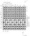
请参阅图2,其为依据本发明实施例所绘示的存储器阵列示意图,其中主要显示出导电通孔、存储节点接垫和钨通孔的位置。如图2所示,存储器阵列1另包含多个V1导电通孔,包括设置在子阵列MAS中的各接垫P1上的导电通孔VA1、设置在带区域SR中的各第一源极线带SLS1上的导电通孔VS1、在各第二源极线带SLS2上的导电通孔VS2和在各字线带WLS上的导电通孔VW。根据本发明实施例,导电通孔VS1和导电通孔VW在第一方向D1上的宽度大于导电通孔VA1在第一方向D1上的宽度。Please refer to FIG. 2 , which is a schematic diagram of a memory array according to an embodiment of the present invention, which mainly shows the positions of conductive vias, storage node pads and tungsten vias. As shown in FIG. 2 , the memory array 1 further includes a plurality of V1 conductive vias, including conductive vias VA1 disposed on the pads P1 in the sub-array MAS, and first source electrodes disposed in the strip region SR Conductive vias VS1 on line strip SLS1 , conductive vias VS2 on each second source line strip SLS2 , and conductive vias VW on each word line strip WLS. According to the embodiment of the present invention, the width of the conductive via VS1 and the conductive via VW in the first direction D1 is greater than the width of the conductive via VA1 in the first direction D1.
根据本发明实施例,存储器阵列1另包含在子阵列MAS中的多个分别电连接至导电通孔VA1且位于M2金属层的存储节点接垫P2、在带区域SR中电连接至导电通孔VS1的接垫PS1、在带区域SR中电连接至导电通孔VS2的接垫PS2,以及在带区域SR中电连接至导电通孔VW的接垫PW。根据本发明实施例,存储节点接垫P2可以具有长方形轮廓,其长边平行于第一方向D1,且与下方的多晶硅栅极线GL部分重叠。根据本发明实施例,存储器阵列1另包含在子阵列MAS中的多个钨通孔140,分别电连接至对应的存储节点接垫P2。根据本发明实施例,多个钨通孔140是交错排列的且大致上分别对准下方的多晶硅栅极线GL。根据本发明实施例,在带区域SR内的接垫PS1、接垫PS2和接垫PW上未布置钨通孔。According to an embodiment of the present invention, the memory array 1 further includes a plurality of storage node pads P2 in the sub-array MAS that are respectively electrically connected to the conductive viasVA1 and located in the M2 metal layer, and are electrically connected to the conductive vias in the strip region SR. Pad PS1 of hole VS1 , pad PS2 electrically connected to conductive via VS2 in strip region SR, and pad PW electrically connected to conductive via VW in strip region SR. According to an embodiment of the present invention, the storage node pad P2 may have a rectangular outline, the long side of which is parallel to the first direction D1 and partially overlaps with the underlying polysilicon gate line GL. According to an embodiment of the present invention, the memory array 1 further includes a plurality of
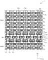
请参阅图3,其为依据本发明实施例所绘示的存储器阵列示意图,其中主要显示出磁存储元件的位置。如图3所示,存储器阵列1的子阵列MAS中包含多个交错的主动磁存储元件MA,带区域SR中包含多个交错的虚设磁存储元件MD。根据本发明实施例,在子阵列MAS中,主动磁存储元件MA设置在对应的钨通孔140上,也就是,主动磁存储元件MA大致上对准下方的钨通孔140,因此,也大致上分别对准下方的多晶硅栅极线GL。主动磁存储元件MA通过钨通孔140电连接到下方的存储节点接垫P2。Please refer to FIG. 3 , which is a schematic diagram of a memory array according to an embodiment of the present invention, wherein the positions of the magnetic storage elements are mainly shown. As shown in FIG. 3 , the sub-array MAS of the memory array 1 includes a plurality of interleaved active magnetic storage elements MA, and the band region SR includesa plurality of interleaved dummy magnetic storage elementsMD . According to the embodiment of the present invention, in the sub- array MAS, the active magnetic storage element MA is disposed on the corresponding tungsten through
根据本发明实施例,主动磁存储元件MA包含布置在一第一列中的多个第一主动磁存储元件MA1和布置在一第二列中的多个第二主动磁存储元件MA2,其中,布置在第一列中的第一主动磁存储元件MA1和布置在第二列中的第二主动磁存储元件MA2分别与沿着第二方向D2延伸的相对应栅极线GL对准。According to an embodiment of the present invention, the active magnetic storage elementMA includes a plurality of first active magnetic storage elements MA1 arranged in a first column and a plurality of second active magnetic storage elementsMA2 arranged in a second column , wherein the first active magnetic storage element MA1 arranged in the first column and the second active magnetic storage element MA2 arranged in the second column are respectively associated with corresponding gate lines GL extending along the second direction D2 alignment.
根据本发明实施例,主动磁存储元件MA和虚设磁存储元件MD包含磁隧穿结(MTJ)元件。根据本发明实施例,MTJ元件可以包含多层结构,例如,一底电极、一上电极,以及位于底电极和上电极之间的一磁隧穿结结构,包括,但不限于,一参考层、一通道层、一自由层和一上盖层。根据本发明实施例,虚设磁存储元件MD的MTJ元件(虚设MTJ元件)的底电极未电连接到源极线带或字线带。According to an embodiment of the present invention, the active magnetic storage elementMA and the dummy magnetic storage elementMD include magnetic tunnel junction (MTJ) elements. According to embodiments of the present invention, the MTJ element may include a multi-layer structure, for example, a bottom electrode, a top electrode, and a magnetic tunnel junction structure between the bottom electrode and the top electrode, including, but not limited to, a reference layer , a channel layer, a free layer and a capping layer. According to an embodiment of the present invention, the bottom electrode of the MTJ element (dummyMTJ element) of the dummy magnetic storage element MD is not electrically connected to the source line strip or the word line strip.
根据本发明实施例,虚设磁存储元件MD以交错方式分别设置在带区域SR内的接垫PS1、接垫PS2和接垫PW上。由于在带区域SR内的接垫PS1、接垫PS2和接垫PW上未布置钨通孔,因此,虚设磁存储元件MD的下电极不会直接电连接至带区域SR内的接垫PS1、接垫PS2和接垫PW。根据本发明实施例,虚设磁存储元件MD与接垫PS1之间、虚设磁存储元件MD与接垫PS2之间、虚设磁存储元件MD与接垫PW之间只有介电层。According to an embodiment of the present invention, the dummy magnetic storage elements MD are respectively disposed on the pads PS1 , PS2 and PW in the strip region SR in astaggered manner. Since no tungsten through-holes are arranged on the pads PS1 , PS2 and PW in the strip region SR, the lower electrode of thedummy magnetic storage element MD is not directly electrically connected to the pads in the strip region SR. Pad PS1 , pad PS2 and pad PW . According to the embodiment of the present invention, there is only dielectric between the dummy magnetic storage elementMD and the pad PS1 , between the dummy magnetic storage elementMD and the pad PS2 , and between the dummy magnetic storage elementMD and the pad PW Floor.
根据本发明实施例,交错排列的主动磁存储元件MA和交错排列的虚设磁存储元件MD被均匀地分布在两个子阵列MAS和带区域SR上。这样的均匀且重复的磁存储元件排列方式,可以具体实现高密度的存储器布局。According to an embodiment of the present invention, the staggered active magnetic storage elementsMA and the staggered dummy magnetic storage elementsMD are uniformly distributed on the two sub-arrays MAS and the strip region SR. Such a uniform and repeated arrangement of magnetic storage elements can specifically realize a high-density memory layout.
请参阅图4,其为依据本发明实施例所绘示的存储器阵列示意图,其中主要显示出带区域SR中的V2导电通孔的位置。如图4所示,存储器阵列1在带区域SR中另设置有交错的导电通孔VPS1、导电通孔VPW和导电通孔VPS2,其中,导电通孔VPS1、导电通孔VPW和导电通孔VPS2分别与下方的接垫PS1、接垫PW和接垫PS2电连接。Please refer to FIG. 4 , which is a schematic diagram of a memory array according to an embodiment of the present invention, which mainly shows the positions of the V2 conductive vias in the strip region SR. As shown in FIG. 4 , the memory array 1 is further provided with staggered conductive vias VPS1 , VPW and VPS2 in the strip region SR, wherein the conductive vias VPS1 , VPW and the conductive via VPS2 are respectively electrically connected to the lower pad PS1 , the pad PW and the pad PS2 .
请参阅图5,其为依据本发明实施例所绘示的存储器阵列示意图,其中主要显示出带区域SR中的位于M3金属层的接垫的位置。如图5所示,存储器阵列1在带区域SR中另设置有位于M3金属层的接垫PVS1、接垫PVW和接垫PVS2,其中,接垫PVS1、接垫PVW和接垫PVS2的尺寸和位置大致上与下方的第一源极线带SLS1、字线带WLS和第二源极线带SLS2相同。Please refer to FIG. 5 , which is a schematic diagram of a memory array according to an embodiment of the present invention, which mainly shows the positions of the pads in the M3 metal layer in the strip region SR. As shown in FIG. 5 , the memory array 1 is further provided with pads PVS1 , PVW and P VS2 located in the M3 metal layer in the strip region SR, wherein the pads PVS1 , the pads PVW and the pads PVS2 The size and location of pad PVS2 is substantially the same as the underlying first source line strip SLS1 , word line strip WLS, and second source line strip SLS2 .
根据本发明实施例,接垫PVS1覆盖导电通孔VPS1和相邻的虚设磁存储元件MD,并将虚设磁存储元件MD的上电极电连接至导电通孔VPS1。根据本发明实施例,接垫PVS2覆盖导电通孔VPS2和相邻的虚设磁存储元件MD,并将虚设磁存储元件MD的上电极电连接至导电通孔VPS2。根据本发明实施例,接垫PVW覆盖导电通孔VPW和相邻的虚设磁存储元件MD,并将虚设磁存储元件MD的上电极电连接至导电通孔VPW。According to an embodiment of the present invention, the pad PVS1 covers the conductive via VPS1 and the adjacent dummy magnetic storage elementMD , and electricallyconnects the upper electrode of the dummy magnetic storage element MD to the conductive via VPS1 . According to an embodiment of the present invention, the pad PVS2 covers the conductive via VPS2 and the adjacent dummy magnetic storage elementMD , and electricallyconnects the upper electrode of the dummy magnetic storage element MD to the conductive via VPS2 . According to an embodiment of the present invention, the pads PVW cover the conductive viasVPW and the adjacent dummy magnetic storage elementsMD , and electrically connect the upper electrodes of the dummy magnetic storage elementsMD to the conductive vias VPW.
请参阅图6,其为沿着图5中切线I-I’所示的剖面示意图,其中,相同的区域、层或元件仍以相同的符号来表示。如图6所示,在半导体基底100上可以有多层介电层,例如,介电层210~260,如前所述,在虚设磁存储元件MD的下电极BE和下方的接垫PS2之间只有介电层230,故虚设磁存储元件MD的下电极BE未直接连接到下方的接垫PS2。根据本发明实施例,导电通孔VPS2可以贯穿介电层230~250,而电连接至下方的接垫PS2。接垫PVS2覆盖导电通孔VPS2和虚设磁存储元件MD,并将虚设磁存储元件MD的上电极TE电连接至导电通孔VPS2。Please refer to FIG. 6 , which is a schematic cross-sectional view along the tangent line II′ in FIG. 5 , wherein the same regions, layers or elements are still denoted by the same symbols. As shown in FIG. 6, there may be multiple dielectric layers on the
请参阅图7,其为依据本发明实施例所绘示的存储器阵列示意图,其中主要显示出V3导电通孔的布局。如图7所示,存储器阵列1在子阵列MAS中另包含多个交错排列的导电通孔VA3,其大致上对准相对应的主动磁存储元件MA,也就是,在子阵列MAS中,各导电通孔VA3直接电连接至各主动磁存储元件MA的上电极。根据本发明实施例,在带区域SR中,设置有多个交错排列的导电通孔VDS31、导电通孔VDW3和导电通孔VDS32,分别电连接至接垫PVS1、接垫PVW和接垫PVS2。根据本发明实施例,导电通孔VDS31、导电通孔VDW3和导电通孔VDS32具有长方形的轮廓,其长边平行于第一方向D1,且各导电通孔VDS31、导电通孔VDW3和导电通孔VDS32的面积大于各导电通孔VA3。Please refer to FIG. 7 , which is a schematic diagram of a memory array according to an embodiment of the present invention, which mainly shows the layout of the V3 conductive via. As shown in FIG. 7 , the memory array 1 further includes a plurality of staggered conductive vias VA3 in the sub-array MAS, which are substantially aligned with the corresponding active magnetic storage elements MA , that is, in the sub- array MAS , each conductive viaVA3 is directly electrically connected to the upper electrode of each active magnetic storage elementMA . According to the embodiment of the present invention, in the strip region SR, a plurality of staggered conductive vias VDS31 , VDW3 and VDS32 are provided, which are electrically connected to the pads PVS1 and PVW respectively. and pad PVS2 . According to the embodiment of the present invention, the conductive via VDS31 , the conductive via VDW3 and the conductive via VDS32 have a rectangular outline, the long sides of which are parallel to the first direction D1, and the conductive via VDS31 , the conductive via V The area ofDW3 and conductive via VDS32 is larger than that of each conductive via VA3 .
请参阅图8,其为依据本发明实施例所绘示的存储器阵列示意图,其中主要显示出M4金属层的布局。如图8所示,存储器阵列1在子阵列MAS中另包含多条位于M4金属层的位线BL,在第一方向D1上电连接至同一行上相对应的导电通孔VA3。根据本发明实施例,在带区域SR中,相对应于导电通孔VDS31、导电通孔VDW3和导电通孔VDS32设置有多个交错排列的接垫PDS41、接垫PDW4和接垫PDS42。Please refer to FIG. 8 , which is a schematic diagram of a memory array according to an embodiment of the present invention, which mainly shows the layout of the M4 metal layer. As shown in FIG. 8 , the memory array 1 further includes a plurality of bit lines BL in the M4 metal layer in the sub-array MAS, which are electrically connected to the corresponding conductive vias VA3 in the same row in the first direction D1 . According to an embodiment of the present invention, in the band region SR, a plurality of staggered pads PDS41 , PDW4 and pads are disposed corresponding to the conductive vias VDS31 , VDW3 and VDS32 . Pad PDS42 .
请参阅图9,其为依据本发明实施例所绘示的存储器阵列示意图,其中主要显示出V4导电通孔的布局。如图9所示,存储器阵列1在带区域SR中,相对应于接垫PDS41、接垫PDW4和接垫PDS42设置有多个交错排列的导电通孔VDS41、导电通孔VDW4和导电通孔VDS42。Please refer to FIG. 9 , which is a schematic diagram of a memory array according to an embodiment of the present invention, which mainly shows the layout of the V4 conductive via. As shown in FIG. 9 , in the strip region SR, the memory array 1 is provided with a plurality of staggered conductive vias VDS41 and VDW4 corresponding to the pads PDS41 , PDW4 and PDS42 and conductive via VDS42 .
请参阅图10,其为依据本发明实施例所绘示的存储器阵列示意图,其中主要显示出M5金属层的布局。如图10所示,存储器阵列1另包含多条位于M5金属层的字线WL和源极线SL。字线WL和源极线SL彼此互相平行且沿着第二方向D2延伸。其中,字线WL电连接至相对应的导电通孔VDW4,源极线SL电连接至相对应的导电通孔VDS41和导电通孔VDS42。Please refer to FIG. 10 , which is a schematic diagram of a memory array according to an embodiment of the present invention, which mainly shows the layout of the M5 metal layer. As shown in FIG. 10 , the memory array 1 further includes a plurality of word lines WL and source lines SL located in the M5 metal layer. The word line WL and the source line SL are parallel to each other and extend along the second direction D2. The word line WL is electrically connected to the corresponding conductive via VDW4 , and the source line SL is electrically connected to the corresponding conductive via VDS41 and VDS42 .
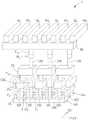
请参阅图11,其为依据本发明实施例所绘示的存储器阵列的子阵列中的部分结构立体示意图,其中,相同的区域、层或元件仍以相同的符号来表示。为方便说明,图中已将介电层省略。如图11所示,晶体管T的漏极区域DD经由漏极接触差塞CD电连接至相对应的接垫P1,再经由导电通孔VA1电连接至相对应的存储节点接垫P2,其中,存储节点接垫P2在第一方向D1上朝向共用源极线上方延伸。在存储节点接垫P2上设有钨通孔140,其中,钨通孔140约略对准下方的栅极线GL。主动磁存储元件MA直接设置在钨通孔140的正上方,而导电通孔VA3直接设置在主动磁存储元件MA的正上方。导电通孔VA3电连接至沿着第一方向D1延伸的位线BL。在位线BL上方则有沿着第二方向D2延伸的字线WL和源极线SL。Please refer to FIG. 11 , which is a schematic perspective view of a part of the structure of a sub-array of a memory array according to an embodiment of the present invention, wherein the same regions, layers or elements are still represented by the same symbols. For convenience of description, the dielectric layer has been omitted in the figure. As shown in FIG. 11 , the drain region DD of the transistorT is electrically connected to the corresponding pad P1 through the drain contact plug CD, and is then electrically connected to the corresponding storage node pad P2 through the conductive viaVA1 . The storage node pads P2 extend toward the top of the common source line in the first direction D1. A tungsten through
请参阅图12,其为依据本发明实施例所绘示的存储器阵列的子阵列MAS和带区域SR中的部分结构立体示意图,其中,相同的区域、层或元件仍以相同的符号来表示。如图12所示,主动磁存储元件MA和虚设磁存储元件MD以交错排列方式均匀的分布在子阵列MAS和带区域SR中,实现了高密度存储器布局。在子阵列MAS内的存储节点接垫P2和在带区域SR内的接垫PS1、接垫PS2和接垫PW在第二方向D1上不是在一条直线上对齐的,而是错置排列的。在带区域SR内的接垫PS1、接垫PS2和接垫PW上未布置钨通孔。虚设磁存储元件MD的下电极不会直接电连接至带区域SR内的接垫PW。导电通孔VPS2电连接至下方的接垫PS2。接垫PVS2覆盖导电通孔VPS2和虚设磁存储元件MD,并将虚设磁存储元件MD的上电极电连接至导电通孔VPS2。从图1中可清楚的看到,位于M1金属层的共同源极线CSL经由第二源极线带SLS2和由构成在V1、M2、V2、M3、V3、M4和V4中的连接路径,电连接至位于M5的源极线SL。Please refer to FIG. 12 , which is a schematic three-dimensional schematic diagram of the sub-array MAS and the strip region SR of the memory array according to an embodiment of the present invention, wherein the same regions, layers or elements are still represented by the same symbols. As shown in FIG. 12 , the active magnetic storage elementsMA and the dummy magnetic storage elements MD are evenly distributed in the sub-array MAS and the strip regionSR in a staggered manner, thereby realizing a high-density memory layout. The storage node pads P2 in the sub-array MAS and the pads PS1 , the pads PS2 and the pads PW in the strip region SR are not aligned in a straight line in the second direction D1, but are displaced arranged. No tungsten vias are arranged on the pads PS1 , PS2 and PW in the strip region SR. The lower electrode of thedummy magnetic storage element MD is not directly electrically connected to the padPW in the strip region SR. The conductive via VPS2 is electrically connected to the underlying pad PS2 . The pad PVS2 covers the conductive via VPS2 and the dummy magnetic storage elementMD , and electricallyconnects the upper electrode of the dummy magnetic storage element MD to the conductive via VPS2 . It can be clearly seen from FIG. 1 that the common source line CSL located in the M1 metal layer, via the second source line strip SLS2 and by the connection paths formed in V1, M2, V2, M3, V3, M4 and V4, Electrically connected to the source line SL at M5.
以上所述仅为本发明的优选实施例,凡依本发明权利要求所做的均等变化与修饰,都应属本发明的涵盖范围。The above descriptions are only preferred embodiments of the present invention, and all equivalent changes and modifications made according to the claims of the present invention shall fall within the scope of the present invention.
Claims (15)
Priority Applications (2)
| Application Number | Priority Date | Filing Date | Title |
|---|---|---|---|
| CN202110198021.9ACN114974339B (en) | 2021-02-22 | 2021-02-22 | Memory array |
| US17/202,296US11737285B2 (en) | 2021-02-22 | 2021-03-15 | Memory array having strap region with staggered dummy magnetic storage elements |
Applications Claiming Priority (1)
| Application Number | Priority Date | Filing Date | Title |
|---|---|---|---|
| CN202110198021.9ACN114974339B (en) | 2021-02-22 | 2021-02-22 | Memory array |
Publications (2)
| Publication Number | Publication Date |
|---|---|
| CN114974339Atrue CN114974339A (en) | 2022-08-30 |
| CN114974339B CN114974339B (en) | 2025-09-16 |
Family
ID=82900912
Family Applications (1)
| Application Number | Title | Priority Date | Filing Date |
|---|---|---|---|
| CN202110198021.9AActiveCN114974339B (en) | 2021-02-22 | 2021-02-22 | Memory array |
Country Status (2)
| Country | Link |
|---|---|
| US (1) | US11737285B2 (en) |
| CN (1) | CN114974339B (en) |
Families Citing this family (2)
| Publication number | Priority date | Publication date | Assignee | Title |
|---|---|---|---|---|
| CN112310144B (en) | 2019-07-29 | 2024-10-15 | 联华电子股份有限公司 | Semiconductor structure and method for manufacturing the same |
| CN116490003A (en)* | 2022-01-14 | 2023-07-25 | 联华电子股份有限公司 | memory array |
Citations (10)
| Publication number | Priority date | Publication date | Assignee | Title |
|---|---|---|---|---|
| US20030235070A1 (en)* | 2002-06-25 | 2003-12-25 | Renesas Technology Corp. | Thin film magnetic memory device and semiconductor integrated circuit device including the same as one of circuit blocks |
| US20040004856A1 (en)* | 2002-07-04 | 2004-01-08 | Nec Corporation | Magnetic random access memory |
| US20060007727A1 (en)* | 2002-09-12 | 2006-01-12 | Griffith University | Memory cell |
| US20060181943A1 (en)* | 2005-02-15 | 2006-08-17 | Samsung Electronics Co., Ltd. | Memory device having open bit line architecture for improving repairability and method of repairing the same |
| CN101971336A (en)* | 2007-12-27 | 2011-02-09 | 桑迪士克3D公司 | Three-dimensional hexagonal matrix memory array and method of fabrication |
| US20120314469A1 (en)* | 2011-06-08 | 2012-12-13 | Kabushiki Kaisha Toshiba | Semiconductor storage device |
| CN103403806A (en)* | 2011-02-25 | 2013-11-20 | 高通股份有限公司 | Configurable memory array |
| US20150069480A1 (en)* | 2013-09-09 | 2015-03-12 | Hiroyuki Kanaya | Magnetic memory and manufacturing method thereof |
| CN106531203A (en)* | 2010-10-08 | 2017-03-22 | 高通股份有限公司 | Magnetic random access memory (mram)layout with uniform pattern |
| CN112234077A (en)* | 2019-07-15 | 2021-01-15 | 联华电子股份有限公司 | Magnetic storage unit and method of making the same |
Family Cites Families (14)
| Publication number | Priority date | Publication date | Assignee | Title |
|---|---|---|---|---|
| US6256224B1 (en)* | 2000-05-03 | 2001-07-03 | Hewlett-Packard Co | Write circuit for large MRAM arrays |
| US5986925A (en)* | 1998-04-07 | 1999-11-16 | Motorola, Inc. | Magnetoresistive random access memory device providing simultaneous reading of two cells and operating method |
| JP4726290B2 (en)* | 2000-10-17 | 2011-07-20 | ルネサスエレクトロニクス株式会社 | Semiconductor integrated circuit |
| US6466475B1 (en)* | 2001-10-31 | 2002-10-15 | Hewlett-Packard Company | Uniform magnetic environment for cells in an MRAM array |
| US7804706B2 (en)* | 2008-11-17 | 2010-09-28 | Magic Technologies, Inc. | Bottom electrode mask design for ultra-thin interlayer dielectric approach in MRAM device fabrication |
| JP4945592B2 (en)* | 2009-03-13 | 2012-06-06 | 株式会社東芝 | Semiconductor memory device |
| JP2012059326A (en)* | 2010-09-10 | 2012-03-22 | Toshiba Corp | Semiconductor storage device |
| JP5518777B2 (en)* | 2011-03-25 | 2014-06-11 | 株式会社東芝 | Semiconductor memory device |
| JP5677186B2 (en)* | 2011-05-06 | 2015-02-25 | 株式会社東芝 | Semiconductor memory device |
| US9698200B2 (en)* | 2015-10-08 | 2017-07-04 | Globalfoundries Singapore Pte. Ltd. | Magnetism-controllable dummy structures in memory device |
| TWI609379B (en)* | 2016-04-26 | 2017-12-21 | 來揚科技股份有限公司 | Peak current bypass protection control device applicable in mram |
| US10374005B2 (en)* | 2017-12-29 | 2019-08-06 | Globalfoundries Singapore Pte. Ltd. | Density-controllable dummy fill strategy for near-MRAM periphery and far-outside-MRAM logic regions for embedded MRAM technology and method for producing the same |
| KR102709416B1 (en)* | 2019-06-03 | 2024-09-24 | 삼성전자주식회사 | A three dimensional memory device |
| US11283005B2 (en)* | 2019-09-30 | 2022-03-22 | Taiwan Semiconductor Manufacturing Company, Ltd. | Spacer scheme and method for MRAM |
- 2021
- 2021-02-22CNCN202110198021.9Apatent/CN114974339B/enactiveActive
- 2021-03-15USUS17/202,296patent/US11737285B2/enactiveActive
Patent Citations (11)
| Publication number | Priority date | Publication date | Assignee | Title |
|---|---|---|---|---|
| US20030235070A1 (en)* | 2002-06-25 | 2003-12-25 | Renesas Technology Corp. | Thin film magnetic memory device and semiconductor integrated circuit device including the same as one of circuit blocks |
| US20040004856A1 (en)* | 2002-07-04 | 2004-01-08 | Nec Corporation | Magnetic random access memory |
| US20060007727A1 (en)* | 2002-09-12 | 2006-01-12 | Griffith University | Memory cell |
| US20060181943A1 (en)* | 2005-02-15 | 2006-08-17 | Samsung Electronics Co., Ltd. | Memory device having open bit line architecture for improving repairability and method of repairing the same |
| CN101971336A (en)* | 2007-12-27 | 2011-02-09 | 桑迪士克3D公司 | Three-dimensional hexagonal matrix memory array and method of fabrication |
| CN106531203A (en)* | 2010-10-08 | 2017-03-22 | 高通股份有限公司 | Magnetic random access memory (mram)layout with uniform pattern |
| CN103403806A (en)* | 2011-02-25 | 2013-11-20 | 高通股份有限公司 | Configurable memory array |
| US20140043924A1 (en)* | 2011-02-25 | 2014-02-13 | Qualcomm Incorporated | Configurable memory array |
| US20120314469A1 (en)* | 2011-06-08 | 2012-12-13 | Kabushiki Kaisha Toshiba | Semiconductor storage device |
| US20150069480A1 (en)* | 2013-09-09 | 2015-03-12 | Hiroyuki Kanaya | Magnetic memory and manufacturing method thereof |
| CN112234077A (en)* | 2019-07-15 | 2021-01-15 | 联华电子股份有限公司 | Magnetic storage unit and method of making the same |
Non-Patent Citations (3)
| Title |
|---|
| LIJUN CHEN 等: "A new modified staggered array undulator", ELSEVIER, 21 May 2019 (2019-05-21)* |
| 李晓燕 等: "阻变存储器无源高密度交叉阵列研究进展", 科学通报, no. 2, 27 September 2018 (2018-09-27)* |
| 鲍旭恒;吴艳艳: "高密度存储器技术发展与应用浅谈", 河南科技, no. 21, 5 November 2015 (2015-11-05)* |
Also Published As
| Publication number | Publication date |
|---|---|
| US20220271088A1 (en) | 2022-08-25 |
| CN114974339B (en) | 2025-09-16 |
| US11737285B2 (en) | 2023-08-22 |
Similar Documents
| Publication | Publication Date | Title |
|---|---|---|
| US8391041B2 (en) | Magnetic memory device | |
| CN100367404C (en) | thin film magnetic memory | |
| US9224786B2 (en) | Semiconductor storage device | |
| US9129893B2 (en) | Semiconductor device | |
| JP4570328B2 (en) | Serial MRAM element | |
| CN112234077B (en) | Magnetic memory cell and method of making the same | |
| KR100923298B1 (en) | MRAM, in which a unit cell consists of one transistor and two MTVs, and a manufacturing method thereof | |
| US20030128580A1 (en) | High-density magnetic random access memory device and method of operating the same | |
| US6542398B2 (en) | Magnetic random access memory | |
| CN1921004B (en) | Magnetic memory device and manufacturing method thereof | |
| US6838721B2 (en) | Integrated circuit with a transitor over an interconnect layer | |
| CN114974339B (en) | Memory array | |
| CN112447219A (en) | Memory layout structure | |
| US7613035B2 (en) | Magnetic memory device and method of writing into the same | |
| KR20140102993A (en) | Magnetic Random Access Memory(MRAM) having increased On/Off ratio and methods of manufacturing and operating the same | |
| JP2005191523A (en) | Magnetic ram | |
| KR100979350B1 (en) | Magnetic ram and method of manufacturing the same | |
| US12317510B2 (en) | Memory array | |
| US20040165427A1 (en) | Magnetic memories having magnetic tunnel junctions in recessed bit lines and/or digit lines and methods of fabricating the same | |
| US11903325B2 (en) | Magnetic memory device having shared source line and bit line | |
| CN112992965B (en) | Layout pattern for MRAM | |
| US20230157032A1 (en) | Bit-line resistance reduction |
Legal Events
| Date | Code | Title | Description |
|---|---|---|---|
| PB01 | Publication | ||
| PB01 | Publication | ||
| SE01 | Entry into force of request for substantive examination | ||
| SE01 | Entry into force of request for substantive examination | ||
| GR01 | Patent grant | ||
| GR01 | Patent grant |