CN114968366A - System and method for improving cache efficiency and utilization - Google Patents
System and method for improving cache efficiency and utilizationDownload PDFInfo
- Publication number
- CN114968366A CN114968366ACN202210586709.9ACN202210586709ACN114968366ACN 114968366 ACN114968366 ACN 114968366ACN 202210586709 ACN202210586709 ACN 202210586709ACN 114968366 ACN114968366 ACN 114968366A
- Authority
- CN
- China
- Prior art keywords
- graphics
- cache
- memory
- processor
- data
- Prior art date
- Legal status (The legal status is an assumption and is not a legal conclusion. Google has not performed a legal analysis and makes no representation as to the accuracy of the status listed.)
- Pending
Links
Images


Classifications
- G—PHYSICS
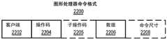
- G06—COMPUTING OR CALCULATING; COUNTING
- G06F—ELECTRIC DIGITAL DATA PROCESSING
- G06F9/00—Arrangements for program control, e.g. control units
- G06F9/06—Arrangements for program control, e.g. control units using stored programs, i.e. using an internal store of processing equipment to receive or retain programs
- G06F9/46—Multiprogramming arrangements
- G06F9/50—Allocation of resources, e.g. of the central processing unit [CPU]
- G06F9/5061—Partitioning or combining of resources
- G06F9/5066—Algorithms for mapping a plurality of inter-dependent sub-tasks onto a plurality of physical CPUs
- G—PHYSICS
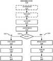
- G06—COMPUTING OR CALCULATING; COUNTING
- G06F—ELECTRIC DIGITAL DATA PROCESSING
- G06F15/00—Digital computers in general; Data processing equipment in general
- G06F15/76—Architectures of general purpose stored program computers
- G06F15/78—Architectures of general purpose stored program computers comprising a single central processing unit
- G06F15/7839—Architectures of general purpose stored program computers comprising a single central processing unit with memory
- G—PHYSICS
- G06—COMPUTING OR CALCULATING; COUNTING
- G06F—ELECTRIC DIGITAL DATA PROCESSING
- G06F12/00—Accessing, addressing or allocating within memory systems or architectures
- G06F12/02—Addressing or allocation; Relocation
- G06F12/0215—Addressing or allocation; Relocation with look ahead addressing means
- G—PHYSICS
- G06—COMPUTING OR CALCULATING; COUNTING
- G06F—ELECTRIC DIGITAL DATA PROCESSING
- G06F12/00—Accessing, addressing or allocating within memory systems or architectures
- G06F12/02—Addressing or allocation; Relocation
- G06F12/0223—User address space allocation, e.g. contiguous or non contiguous base addressing
- G06F12/023—Free address space management
- G06F12/0238—Memory management in non-volatile memory, e.g. resistive RAM or ferroelectric memory
- G06F12/0246—Memory management in non-volatile memory, e.g. resistive RAM or ferroelectric memory in block erasable memory, e.g. flash memory
- G—PHYSICS
- G06—COMPUTING OR CALCULATING; COUNTING
- G06F—ELECTRIC DIGITAL DATA PROCESSING
- G06F12/00—Accessing, addressing or allocating within memory systems or architectures
- G06F12/02—Addressing or allocation; Relocation
- G06F12/06—Addressing a physical block of locations, e.g. base addressing, module addressing, memory dedication
- G06F12/0607—Interleaved addressing
- G—PHYSICS
- G06—COMPUTING OR CALCULATING; COUNTING
- G06F—ELECTRIC DIGITAL DATA PROCESSING
- G06F12/00—Accessing, addressing or allocating within memory systems or architectures
- G06F12/02—Addressing or allocation; Relocation
- G06F12/08—Addressing or allocation; Relocation in hierarchically structured memory systems, e.g. virtual memory systems
- G06F12/0802—Addressing of a memory level in which the access to the desired data or data block requires associative addressing means, e.g. caches
- G06F12/0804—Addressing of a memory level in which the access to the desired data or data block requires associative addressing means, e.g. caches with main memory updating
- G—PHYSICS
- G06—COMPUTING OR CALCULATING; COUNTING
- G06F—ELECTRIC DIGITAL DATA PROCESSING
- G06F12/00—Accessing, addressing or allocating within memory systems or architectures
- G06F12/02—Addressing or allocation; Relocation
- G06F12/08—Addressing or allocation; Relocation in hierarchically structured memory systems, e.g. virtual memory systems
- G06F12/0802—Addressing of a memory level in which the access to the desired data or data block requires associative addressing means, e.g. caches
- G06F12/0806—Multiuser, multiprocessor or multiprocessing cache systems
- G06F12/0811—Multiuser, multiprocessor or multiprocessing cache systems with multilevel cache hierarchies
- G—PHYSICS
- G06—COMPUTING OR CALCULATING; COUNTING
- G06F—ELECTRIC DIGITAL DATA PROCESSING
- G06F12/00—Accessing, addressing or allocating within memory systems or architectures
- G06F12/02—Addressing or allocation; Relocation
- G06F12/08—Addressing or allocation; Relocation in hierarchically structured memory systems, e.g. virtual memory systems
- G06F12/0802—Addressing of a memory level in which the access to the desired data or data block requires associative addressing means, e.g. caches
- G06F12/0862—Addressing of a memory level in which the access to the desired data or data block requires associative addressing means, e.g. caches with prefetch
- G—PHYSICS
- G06—COMPUTING OR CALCULATING; COUNTING
- G06F—ELECTRIC DIGITAL DATA PROCESSING
- G06F12/00—Accessing, addressing or allocating within memory systems or architectures
- G06F12/02—Addressing or allocation; Relocation
- G06F12/08—Addressing or allocation; Relocation in hierarchically structured memory systems, e.g. virtual memory systems
- G06F12/0802—Addressing of a memory level in which the access to the desired data or data block requires associative addressing means, e.g. caches
- G06F12/0866—Addressing of a memory level in which the access to the desired data or data block requires associative addressing means, e.g. caches for peripheral storage systems, e.g. disk cache
- G06F12/0871—Allocation or management of cache space
- G—PHYSICS
- G06—COMPUTING OR CALCULATING; COUNTING
- G06F—ELECTRIC DIGITAL DATA PROCESSING
- G06F12/00—Accessing, addressing or allocating within memory systems or architectures
- G06F12/02—Addressing or allocation; Relocation
- G06F12/08—Addressing or allocation; Relocation in hierarchically structured memory systems, e.g. virtual memory systems
- G06F12/0802—Addressing of a memory level in which the access to the desired data or data block requires associative addressing means, e.g. caches
- G06F12/0875—Addressing of a memory level in which the access to the desired data or data block requires associative addressing means, e.g. caches with dedicated cache, e.g. instruction or stack
- G—PHYSICS
- G06—COMPUTING OR CALCULATING; COUNTING
- G06F—ELECTRIC DIGITAL DATA PROCESSING
- G06F12/00—Accessing, addressing or allocating within memory systems or architectures
- G06F12/02—Addressing or allocation; Relocation
- G06F12/08—Addressing or allocation; Relocation in hierarchically structured memory systems, e.g. virtual memory systems
- G06F12/0802—Addressing of a memory level in which the access to the desired data or data block requires associative addressing means, e.g. caches
- G06F12/0877—Cache access modes
- G06F12/0882—Page mode
- G—PHYSICS
- G06—COMPUTING OR CALCULATING; COUNTING
- G06F—ELECTRIC DIGITAL DATA PROCESSING
- G06F12/00—Accessing, addressing or allocating within memory systems or architectures
- G06F12/02—Addressing or allocation; Relocation
- G06F12/08—Addressing or allocation; Relocation in hierarchically structured memory systems, e.g. virtual memory systems
- G06F12/0802—Addressing of a memory level in which the access to the desired data or data block requires associative addressing means, e.g. caches
- G06F12/0888—Addressing of a memory level in which the access to the desired data or data block requires associative addressing means, e.g. caches using selective caching, e.g. bypass
- G—PHYSICS
- G06—COMPUTING OR CALCULATING; COUNTING
- G06F—ELECTRIC DIGITAL DATA PROCESSING
- G06F12/00—Accessing, addressing or allocating within memory systems or architectures
- G06F12/02—Addressing or allocation; Relocation
- G06F12/08—Addressing or allocation; Relocation in hierarchically structured memory systems, e.g. virtual memory systems
- G06F12/0802—Addressing of a memory level in which the access to the desired data or data block requires associative addressing means, e.g. caches
- G06F12/0891—Addressing of a memory level in which the access to the desired data or data block requires associative addressing means, e.g. caches using clearing, invalidating or resetting means
- G—PHYSICS
- G06—COMPUTING OR CALCULATING; COUNTING
- G06F—ELECTRIC DIGITAL DATA PROCESSING
- G06F12/00—Accessing, addressing or allocating within memory systems or architectures
- G06F12/02—Addressing or allocation; Relocation
- G06F12/08—Addressing or allocation; Relocation in hierarchically structured memory systems, e.g. virtual memory systems
- G06F12/0802—Addressing of a memory level in which the access to the desired data or data block requires associative addressing means, e.g. caches
- G06F12/0893—Caches characterised by their organisation or structure
- G06F12/0895—Caches characterised by their organisation or structure of parts of caches, e.g. directory or tag array
- G—PHYSICS
- G06—COMPUTING OR CALCULATING; COUNTING
- G06F—ELECTRIC DIGITAL DATA PROCESSING
- G06F12/00—Accessing, addressing or allocating within memory systems or architectures
- G06F12/02—Addressing or allocation; Relocation
- G06F12/08—Addressing or allocation; Relocation in hierarchically structured memory systems, e.g. virtual memory systems
- G06F12/0802—Addressing of a memory level in which the access to the desired data or data block requires associative addressing means, e.g. caches
- G06F12/0893—Caches characterised by their organisation or structure
- G06F12/0897—Caches characterised by their organisation or structure with two or more cache hierarchy levels
- G—PHYSICS
- G06—COMPUTING OR CALCULATING; COUNTING
- G06F—ELECTRIC DIGITAL DATA PROCESSING
- G06F12/00—Accessing, addressing or allocating within memory systems or architectures
- G06F12/02—Addressing or allocation; Relocation
- G06F12/08—Addressing or allocation; Relocation in hierarchically structured memory systems, e.g. virtual memory systems
- G06F12/10—Address translation
- G06F12/1009—Address translation using page tables, e.g. page table structures
- G—PHYSICS
- G06—COMPUTING OR CALCULATING; COUNTING
- G06F—ELECTRIC DIGITAL DATA PROCESSING
- G06F13/00—Interconnection of, or transfer of information or other signals between, memories, input/output devices or central processing units
- G06F13/14—Handling requests for interconnection or transfer
- G06F13/16—Handling requests for interconnection or transfer for access to memory bus
- G06F13/1605—Handling requests for interconnection or transfer for access to memory bus based on arbitration
- G06F13/161—Handling requests for interconnection or transfer for access to memory bus based on arbitration with latency improvement
- G06F13/1626—Handling requests for interconnection or transfer for access to memory bus based on arbitration with latency improvement by reordering requests
- G—PHYSICS
- G06—COMPUTING OR CALCULATING; COUNTING
- G06F—ELECTRIC DIGITAL DATA PROCESSING
- G06F15/00—Digital computers in general; Data processing equipment in general
- G06F15/16—Combinations of two or more digital computers each having at least an arithmetic unit, a program unit and a register, e.g. for a simultaneous processing of several programs
- G06F15/163—Interprocessor communication
- G06F15/173—Interprocessor communication using an interconnection network, e.g. matrix, shuffle, pyramid, star, snowflake
- G—PHYSICS
- G06—COMPUTING OR CALCULATING; COUNTING
- G06F—ELECTRIC DIGITAL DATA PROCESSING
- G06F15/00—Digital computers in general; Data processing equipment in general
- G06F15/76—Architectures of general purpose stored program computers
- G06F15/80—Architectures of general purpose stored program computers comprising an array of processing units with common control, e.g. single instruction multiple data processors
- G06F15/8046—Systolic arrays
- G—PHYSICS
- G06—COMPUTING OR CALCULATING; COUNTING
- G06F—ELECTRIC DIGITAL DATA PROCESSING
- G06F16/00—Information retrieval; Database structures therefor; File system structures therefor
- G06F16/20—Information retrieval; Database structures therefor; File system structures therefor of structured data, e.g. relational data
- G06F16/24—Querying
- G06F16/245—Query processing
- G06F16/24569—Query processing with adaptation to specific hardware, e.g. adapted for using GPUs or SSDs
- G—PHYSICS
- G06—COMPUTING OR CALCULATING; COUNTING
- G06F—ELECTRIC DIGITAL DATA PROCESSING
- G06F17/00—Digital computing or data processing equipment or methods, specially adapted for specific functions
- G06F17/10—Complex mathematical operations
- G06F17/16—Matrix or vector computation, e.g. matrix-matrix or matrix-vector multiplication, matrix factorization
- G—PHYSICS
- G06—COMPUTING OR CALCULATING; COUNTING
- G06F—ELECTRIC DIGITAL DATA PROCESSING
- G06F17/00—Digital computing or data processing equipment or methods, specially adapted for specific functions
- G06F17/10—Complex mathematical operations
- G06F17/18—Complex mathematical operations for evaluating statistical data, e.g. average values, frequency distributions, probability functions, regression analysis
- G—PHYSICS
- G06—COMPUTING OR CALCULATING; COUNTING
- G06F—ELECTRIC DIGITAL DATA PROCESSING
- G06F7/00—Methods or arrangements for processing data by operating upon the order or content of the data handled
- G06F7/38—Methods or arrangements for performing computations using exclusively denominational number representation, e.g. using binary, ternary, decimal representation
- G06F7/48—Methods or arrangements for performing computations using exclusively denominational number representation, e.g. using binary, ternary, decimal representation using non-contact-making devices, e.g. tube, solid state device; using unspecified devices
- G06F7/544—Methods or arrangements for performing computations using exclusively denominational number representation, e.g. using binary, ternary, decimal representation using non-contact-making devices, e.g. tube, solid state device; using unspecified devices for evaluating functions by calculation
- G06F7/5443—Sum of products
- G—PHYSICS
- G06—COMPUTING OR CALCULATING; COUNTING
- G06F—ELECTRIC DIGITAL DATA PROCESSING
- G06F7/00—Methods or arrangements for processing data by operating upon the order or content of the data handled
- G06F7/38—Methods or arrangements for performing computations using exclusively denominational number representation, e.g. using binary, ternary, decimal representation
- G06F7/48—Methods or arrangements for performing computations using exclusively denominational number representation, e.g. using binary, ternary, decimal representation using non-contact-making devices, e.g. tube, solid state device; using unspecified devices
- G06F7/57—Arithmetic logic units [ALU], i.e. arrangements or devices for performing two or more of the operations covered by groups G06F7/483 – G06F7/556 or for performing logical operations
- G06F7/575—Basic arithmetic logic units, i.e. devices selectable to perform either addition, subtraction or one of several logical operations, using, at least partially, the same circuitry
- G—PHYSICS
- G06—COMPUTING OR CALCULATING; COUNTING
- G06F—ELECTRIC DIGITAL DATA PROCESSING
- G06F7/00—Methods or arrangements for processing data by operating upon the order or content of the data handled
- G06F7/58—Random or pseudo-random number generators
- G—PHYSICS
- G06—COMPUTING OR CALCULATING; COUNTING
- G06F—ELECTRIC DIGITAL DATA PROCESSING
- G06F7/00—Methods or arrangements for processing data by operating upon the order or content of the data handled
- G06F7/58—Random or pseudo-random number generators
- G06F7/588—Random number generators, i.e. based on natural stochastic processes
- G—PHYSICS
- G06—COMPUTING OR CALCULATING; COUNTING
- G06F—ELECTRIC DIGITAL DATA PROCESSING
- G06F9/00—Arrangements for program control, e.g. control units
- G06F9/06—Arrangements for program control, e.g. control units using stored programs, i.e. using an internal store of processing equipment to receive or retain programs
- G06F9/30—Arrangements for executing machine instructions, e.g. instruction decode
- G06F9/30003—Arrangements for executing specific machine instructions
- G06F9/30007—Arrangements for executing specific machine instructions to perform operations on data operands
- G06F9/3001—Arithmetic instructions
- G06F9/30014—Arithmetic instructions with variable precision
- G—PHYSICS
- G06—COMPUTING OR CALCULATING; COUNTING
- G06F—ELECTRIC DIGITAL DATA PROCESSING
- G06F9/00—Arrangements for program control, e.g. control units
- G06F9/06—Arrangements for program control, e.g. control units using stored programs, i.e. using an internal store of processing equipment to receive or retain programs
- G06F9/30—Arrangements for executing machine instructions, e.g. instruction decode
- G06F9/30003—Arrangements for executing specific machine instructions
- G06F9/30007—Arrangements for executing specific machine instructions to perform operations on data operands
- G06F9/30036—Instructions to perform operations on packed data, e.g. vector, tile or matrix operations
- G—PHYSICS
- G06—COMPUTING OR CALCULATING; COUNTING
- G06F—ELECTRIC DIGITAL DATA PROCESSING
- G06F9/00—Arrangements for program control, e.g. control units
- G06F9/06—Arrangements for program control, e.g. control units using stored programs, i.e. using an internal store of processing equipment to receive or retain programs
- G06F9/30—Arrangements for executing machine instructions, e.g. instruction decode
- G06F9/30003—Arrangements for executing specific machine instructions
- G06F9/3004—Arrangements for executing specific machine instructions to perform operations on memory
- G06F9/30043—LOAD or STORE instructions; Clear instruction
- G—PHYSICS
- G06—COMPUTING OR CALCULATING; COUNTING
- G06F—ELECTRIC DIGITAL DATA PROCESSING
- G06F9/00—Arrangements for program control, e.g. control units
- G06F9/06—Arrangements for program control, e.g. control units using stored programs, i.e. using an internal store of processing equipment to receive or retain programs
- G06F9/30—Arrangements for executing machine instructions, e.g. instruction decode
- G06F9/30003—Arrangements for executing specific machine instructions
- G06F9/3004—Arrangements for executing specific machine instructions to perform operations on memory
- G06F9/30047—Prefetch instructions; cache control instructions
- G—PHYSICS
- G06—COMPUTING OR CALCULATING; COUNTING
- G06F—ELECTRIC DIGITAL DATA PROCESSING
- G06F9/00—Arrangements for program control, e.g. control units
- G06F9/06—Arrangements for program control, e.g. control units using stored programs, i.e. using an internal store of processing equipment to receive or retain programs
- G06F9/30—Arrangements for executing machine instructions, e.g. instruction decode
- G06F9/30003—Arrangements for executing specific machine instructions
- G06F9/3005—Arrangements for executing specific machine instructions to perform operations for flow control
- G06F9/30065—Loop control instructions; iterative instructions, e.g. LOOP, REPEAT
- G—PHYSICS
- G06—COMPUTING OR CALCULATING; COUNTING
- G06F—ELECTRIC DIGITAL DATA PROCESSING
- G06F9/00—Arrangements for program control, e.g. control units
- G06F9/06—Arrangements for program control, e.g. control units using stored programs, i.e. using an internal store of processing equipment to receive or retain programs
- G06F9/30—Arrangements for executing machine instructions, e.g. instruction decode
- G06F9/30003—Arrangements for executing specific machine instructions
- G06F9/30076—Arrangements for executing specific machine instructions to perform miscellaneous control operations, e.g. NOP
- G06F9/30079—Pipeline control instructions, e.g. multicycle NOP
- G—PHYSICS
- G06—COMPUTING OR CALCULATING; COUNTING
- G06F—ELECTRIC DIGITAL DATA PROCESSING
- G06F9/00—Arrangements for program control, e.g. control units
- G06F9/06—Arrangements for program control, e.g. control units using stored programs, i.e. using an internal store of processing equipment to receive or retain programs
- G06F9/30—Arrangements for executing machine instructions, e.g. instruction decode
- G06F9/38—Concurrent instruction execution, e.g. pipeline or look ahead
- G06F9/3824—Operand accessing
- G06F9/383—Operand prefetching
- G—PHYSICS
- G06—COMPUTING OR CALCULATING; COUNTING
- G06F—ELECTRIC DIGITAL DATA PROCESSING
- G06F9/00—Arrangements for program control, e.g. control units
- G06F9/06—Arrangements for program control, e.g. control units using stored programs, i.e. using an internal store of processing equipment to receive or retain programs
- G06F9/30—Arrangements for executing machine instructions, e.g. instruction decode
- G06F9/38—Concurrent instruction execution, e.g. pipeline or look ahead
- G06F9/3885—Concurrent instruction execution, e.g. pipeline or look ahead using a plurality of independent parallel functional units
- G06F9/3887—Concurrent instruction execution, e.g. pipeline or look ahead using a plurality of independent parallel functional units controlled by a single instruction for multiple data lanes [SIMD]
- G—PHYSICS
- G06—COMPUTING OR CALCULATING; COUNTING
- G06F—ELECTRIC DIGITAL DATA PROCESSING
- G06F9/00—Arrangements for program control, e.g. control units
- G06F9/06—Arrangements for program control, e.g. control units using stored programs, i.e. using an internal store of processing equipment to receive or retain programs
- G06F9/30—Arrangements for executing machine instructions, e.g. instruction decode
- G06F9/38—Concurrent instruction execution, e.g. pipeline or look ahead
- G06F9/3885—Concurrent instruction execution, e.g. pipeline or look ahead using a plurality of independent parallel functional units
- G06F9/3888—Concurrent instruction execution, e.g. pipeline or look ahead using a plurality of independent parallel functional units controlled by a single instruction for multiple threads [SIMT] in parallel
- G—PHYSICS
- G06—COMPUTING OR CALCULATING; COUNTING
- G06F—ELECTRIC DIGITAL DATA PROCESSING
- G06F9/00—Arrangements for program control, e.g. control units
- G06F9/06—Arrangements for program control, e.g. control units using stored programs, i.e. using an internal store of processing equipment to receive or retain programs
- G06F9/46—Multiprogramming arrangements
- G06F9/50—Allocation of resources, e.g. of the central processing unit [CPU]
- G06F9/5005—Allocation of resources, e.g. of the central processing unit [CPU] to service a request
- G06F9/5011—Allocation of resources, e.g. of the central processing unit [CPU] to service a request the resources being hardware resources other than CPUs, Servers and Terminals
- G—PHYSICS
- G06—COMPUTING OR CALCULATING; COUNTING
- G06F—ELECTRIC DIGITAL DATA PROCESSING
- G06F9/00—Arrangements for program control, e.g. control units
- G06F9/06—Arrangements for program control, e.g. control units using stored programs, i.e. using an internal store of processing equipment to receive or retain programs
- G06F9/46—Multiprogramming arrangements
- G06F9/50—Allocation of resources, e.g. of the central processing unit [CPU]
- G06F9/5061—Partitioning or combining of resources
- G06F9/5077—Logical partitioning of resources; Management or configuration of virtualized resources
- G—PHYSICS
- G06—COMPUTING OR CALCULATING; COUNTING
- G06N—COMPUTING ARRANGEMENTS BASED ON SPECIFIC COMPUTATIONAL MODELS
- G06N3/00—Computing arrangements based on biological models
- G06N3/02—Neural networks
- G06N3/04—Architecture, e.g. interconnection topology
- G06N3/044—Recurrent networks, e.g. Hopfield networks
- G06N3/0442—Recurrent networks, e.g. Hopfield networks characterised by memory or gating, e.g. long short-term memory [LSTM] or gated recurrent units [GRU]
- G—PHYSICS
- G06—COMPUTING OR CALCULATING; COUNTING
- G06N—COMPUTING ARRANGEMENTS BASED ON SPECIFIC COMPUTATIONAL MODELS
- G06N3/00—Computing arrangements based on biological models
- G06N3/02—Neural networks
- G06N3/04—Architecture, e.g. interconnection topology
- G06N3/0464—Convolutional networks [CNN, ConvNet]
- G—PHYSICS
- G06—COMPUTING OR CALCULATING; COUNTING
- G06N—COMPUTING ARRANGEMENTS BASED ON SPECIFIC COMPUTATIONAL MODELS
- G06N3/00—Computing arrangements based on biological models
- G06N3/02—Neural networks
- G06N3/08—Learning methods
- G06N3/0895—Weakly supervised learning, e.g. semi-supervised or self-supervised learning
- G—PHYSICS
- G06—COMPUTING OR CALCULATING; COUNTING
- G06N—COMPUTING ARRANGEMENTS BASED ON SPECIFIC COMPUTATIONAL MODELS
- G06N3/00—Computing arrangements based on biological models
- G06N3/02—Neural networks
- G06N3/08—Learning methods
- G06N3/09—Supervised learning
- G—PHYSICS
- G06—COMPUTING OR CALCULATING; COUNTING
- G06N—COMPUTING ARRANGEMENTS BASED ON SPECIFIC COMPUTATIONAL MODELS
- G06N3/00—Computing arrangements based on biological models
- G06N3/02—Neural networks
- G06N3/08—Learning methods
- G06N3/098—Distributed learning, e.g. federated learning
- G—PHYSICS
- G06—COMPUTING OR CALCULATING; COUNTING
- G06T—IMAGE DATA PROCESSING OR GENERATION, IN GENERAL
- G06T1/00—General purpose image data processing
- G06T1/20—Processor architectures; Processor configuration, e.g. pipelining
- G—PHYSICS
- G06—COMPUTING OR CALCULATING; COUNTING
- G06T—IMAGE DATA PROCESSING OR GENERATION, IN GENERAL
- G06T1/00—General purpose image data processing
- G06T1/60—Memory management
- H—ELECTRICITY
- H03—ELECTRONIC CIRCUITRY
- H03M—CODING; DECODING; CODE CONVERSION IN GENERAL
- H03M7/00—Conversion of a code where information is represented by a given sequence or number of digits to a code where the same, similar or subset of information is represented by a different sequence or number of digits
- H03M7/30—Compression; Expansion; Suppression of unnecessary data, e.g. redundancy reduction
- H03M7/46—Conversion to or from run-length codes, i.e. by representing the number of consecutive digits, or groups of digits, of the same kind by a code word and a digit indicative of that kind
- G—PHYSICS
- G06—COMPUTING OR CALCULATING; COUNTING
- G06F—ELECTRIC DIGITAL DATA PROCESSING
- G06F12/00—Accessing, addressing or allocating within memory systems or architectures
- G06F12/02—Addressing or allocation; Relocation
- G06F12/08—Addressing or allocation; Relocation in hierarchically structured memory systems, e.g. virtual memory systems
- G06F12/12—Replacement control
- G06F12/121—Replacement control using replacement algorithms
- G06F12/128—Replacement control using replacement algorithms adapted to multidimensional cache systems, e.g. set-associative, multicache, multiset or multilevel
- G—PHYSICS
- G06—COMPUTING OR CALCULATING; COUNTING
- G06F—ELECTRIC DIGITAL DATA PROCESSING
- G06F2212/00—Indexing scheme relating to accessing, addressing or allocation within memory systems or architectures
- G06F2212/10—Providing a specific technical effect
- G06F2212/1008—Correctness of operation, e.g. memory ordering
- G—PHYSICS
- G06—COMPUTING OR CALCULATING; COUNTING
- G06F—ELECTRIC DIGITAL DATA PROCESSING
- G06F2212/00—Indexing scheme relating to accessing, addressing or allocation within memory systems or architectures
- G06F2212/10—Providing a specific technical effect
- G06F2212/1016—Performance improvement
- G06F2212/1021—Hit rate improvement
- G—PHYSICS
- G06—COMPUTING OR CALCULATING; COUNTING
- G06F—ELECTRIC DIGITAL DATA PROCESSING
- G06F2212/00—Indexing scheme relating to accessing, addressing or allocation within memory systems or architectures
- G06F2212/10—Providing a specific technical effect
- G06F2212/1016—Performance improvement
- G06F2212/1024—Latency reduction
- G—PHYSICS
- G06—COMPUTING OR CALCULATING; COUNTING
- G06F—ELECTRIC DIGITAL DATA PROCESSING
- G06F2212/00—Indexing scheme relating to accessing, addressing or allocation within memory systems or architectures
- G06F2212/10—Providing a specific technical effect
- G06F2212/1041—Resource optimization
- G06F2212/1044—Space efficiency improvement
- G—PHYSICS
- G06—COMPUTING OR CALCULATING; COUNTING
- G06F—ELECTRIC DIGITAL DATA PROCESSING
- G06F2212/00—Indexing scheme relating to accessing, addressing or allocation within memory systems or architectures
- G06F2212/25—Using a specific main memory architecture
- G06F2212/254—Distributed memory
- G06F2212/2542—Non-uniform memory access [NUMA] architecture
- G—PHYSICS
- G06—COMPUTING OR CALCULATING; COUNTING
- G06F—ELECTRIC DIGITAL DATA PROCESSING
- G06F2212/00—Indexing scheme relating to accessing, addressing or allocation within memory systems or architectures
- G06F2212/30—Providing cache or TLB in specific location of a processing system
- G06F2212/302—In image processor or graphics adapter
- G—PHYSICS
- G06—COMPUTING OR CALCULATING; COUNTING
- G06F—ELECTRIC DIGITAL DATA PROCESSING
- G06F2212/00—Indexing scheme relating to accessing, addressing or allocation within memory systems or architectures
- G06F2212/40—Specific encoding of data in memory or cache
- G06F2212/401—Compressed data
- G—PHYSICS
- G06—COMPUTING OR CALCULATING; COUNTING
- G06F—ELECTRIC DIGITAL DATA PROCESSING
- G06F2212/00—Indexing scheme relating to accessing, addressing or allocation within memory systems or architectures
- G06F2212/45—Caching of specific data in cache memory
- G06F2212/455—Image or video data
- G—PHYSICS
- G06—COMPUTING OR CALCULATING; COUNTING
- G06F—ELECTRIC DIGITAL DATA PROCESSING
- G06F2212/00—Indexing scheme relating to accessing, addressing or allocation within memory systems or architectures
- G06F2212/60—Details of cache memory
- G—PHYSICS
- G06—COMPUTING OR CALCULATING; COUNTING
- G06F—ELECTRIC DIGITAL DATA PROCESSING
- G06F2212/00—Indexing scheme relating to accessing, addressing or allocation within memory systems or architectures
- G06F2212/60—Details of cache memory
- G06F2212/601—Reconfiguration of cache memory
- G—PHYSICS
- G06—COMPUTING OR CALCULATING; COUNTING
- G06F—ELECTRIC DIGITAL DATA PROCESSING
- G06F2212/00—Indexing scheme relating to accessing, addressing or allocation within memory systems or architectures
- G06F2212/60—Details of cache memory
- G06F2212/6026—Prefetching based on access pattern detection, e.g. stride based prefetch
- G—PHYSICS
- G06—COMPUTING OR CALCULATING; COUNTING
- G06F—ELECTRIC DIGITAL DATA PROCESSING
- G06F2212/00—Indexing scheme relating to accessing, addressing or allocation within memory systems or architectures
- G06F2212/60—Details of cache memory
- G06F2212/6028—Prefetching based on hints or prefetch instructions
- G—PHYSICS
- G06—COMPUTING OR CALCULATING; COUNTING
- G06F—ELECTRIC DIGITAL DATA PROCESSING
- G06F2212/00—Indexing scheme relating to accessing, addressing or allocation within memory systems or architectures
- G06F2212/60—Details of cache memory
- G06F2212/608—Details relating to cache mapping
- G—PHYSICS
- G06—COMPUTING OR CALCULATING; COUNTING
- G06F—ELECTRIC DIGITAL DATA PROCESSING
- G06F2212/00—Indexing scheme relating to accessing, addressing or allocation within memory systems or architectures
- G06F2212/65—Details of virtual memory and virtual address translation
- G06F2212/652—Page size control
- G—PHYSICS
- G06—COMPUTING OR CALCULATING; COUNTING
- G06F—ELECTRIC DIGITAL DATA PROCESSING
- G06F9/00—Arrangements for program control, e.g. control units
- G06F9/06—Arrangements for program control, e.g. control units using stored programs, i.e. using an internal store of processing equipment to receive or retain programs
- G06F9/30—Arrangements for executing machine instructions, e.g. instruction decode
- G06F9/38—Concurrent instruction execution, e.g. pipeline or look ahead
- G06F9/3802—Instruction prefetching
- G—PHYSICS
- G06—COMPUTING OR CALCULATING; COUNTING
- G06F—ELECTRIC DIGITAL DATA PROCESSING
- G06F9/00—Arrangements for program control, e.g. control units
- G06F9/06—Arrangements for program control, e.g. control units using stored programs, i.e. using an internal store of processing equipment to receive or retain programs
- G06F9/30—Arrangements for executing machine instructions, e.g. instruction decode
- G06F9/38—Concurrent instruction execution, e.g. pipeline or look ahead
- G06F9/3818—Decoding for concurrent execution
- G—PHYSICS
- G06—COMPUTING OR CALCULATING; COUNTING
- G06F—ELECTRIC DIGITAL DATA PROCESSING
- G06F9/00—Arrangements for program control, e.g. control units
- G06F9/06—Arrangements for program control, e.g. control units using stored programs, i.e. using an internal store of processing equipment to receive or retain programs
- G06F9/30—Arrangements for executing machine instructions, e.g. instruction decode
- G06F9/38—Concurrent instruction execution, e.g. pipeline or look ahead
- G06F9/3867—Concurrent instruction execution, e.g. pipeline or look ahead using instruction pipelines
- G—PHYSICS
- G06—COMPUTING OR CALCULATING; COUNTING
- G06N—COMPUTING ARRANGEMENTS BASED ON SPECIFIC COMPUTATIONAL MODELS
- G06N3/00—Computing arrangements based on biological models
- G06N3/02—Neural networks
- G06N3/08—Learning methods
- G—PHYSICS
- G06—COMPUTING OR CALCULATING; COUNTING
- G06T—IMAGE DATA PROCESSING OR GENERATION, IN GENERAL
- G06T15/00—3D [Three Dimensional] image rendering
- G06T15/06—Ray-tracing
Landscapes
- Engineering & Computer Science (AREA)
- Theoretical Computer Science (AREA)
- Physics & Mathematics (AREA)
- General Physics & Mathematics (AREA)
- General Engineering & Computer Science (AREA)
- Software Systems (AREA)
- Mathematical Optimization (AREA)
- Pure & Applied Mathematics (AREA)
- Mathematical Analysis (AREA)
- Computational Mathematics (AREA)
- Mathematical Physics (AREA)
- Computing Systems (AREA)
- Computer Hardware Design (AREA)
- Data Mining & Analysis (AREA)
- Life Sciences & Earth Sciences (AREA)
- Computational Linguistics (AREA)
- Biophysics (AREA)
- Molecular Biology (AREA)
- General Health & Medical Sciences (AREA)
- Evolutionary Computation (AREA)
- Biomedical Technology (AREA)
- Artificial Intelligence (AREA)
- Health & Medical Sciences (AREA)
- Databases & Information Systems (AREA)
- Algebra (AREA)
- Evolutionary Biology (AREA)
- Bioinformatics & Computational Biology (AREA)
- Bioinformatics & Cheminformatics (AREA)
- Operations Research (AREA)
- Probability & Statistics with Applications (AREA)
- Image Generation (AREA)
- Image Processing (AREA)
- Advance Control (AREA)
- Executing Machine-Instructions (AREA)
- Computer Graphics (AREA)
- Memory System Of A Hierarchy Structure (AREA)
- Complex Calculations (AREA)
- Memory System (AREA)
Abstract
Translated fromChinese
Description
Translated fromChinese本发明专利申请是国际申请号为PCT/US2020/022837,国际申请日为2020年3月14日,进入中国国家阶段的申请号为202080011587.X,名称为“用于提高高速缓存效率和利用率的系统和方法”的发明专利申请的分案申请。The patent application of the present invention is the international application number PCT/US2020/022837, the international application date is March 14, 2020, the application number entering the Chinese national phase is 202080011587.X, and the name is "For improving cache efficiency and utilization rate" The system and method" of the divisional application of the invention patent application.
相关申请的交叉引用CROSS-REFERENCE TO RELATED APPLICATIONS
本申请关于2019年3月15日提交的Abhishek Appu等人的题为“GRAPHICSPROCESSING(图形处理)”的美国临时申请62/819,337(代理人案卷号AC0271-Z)、2019年3月15日提交的Lakshminarayanan Striramassarma等人的题为“GRAPHICS DATA PROCESSING(图形数据处理)”的美国临时申请62/819,435(代理人案卷号AC0285-Z)、以及2019年3月15日提交的Subramaniam Maiyuran等人的题为“SYSTEMS AND METHODS FOR PARTITIONINGCACHE TO REDUCE CACHE ACCESS LATENCY(用于对高速缓存分区以减少高速缓存访问等待时间的系统和方法)”的美国临时申请62/819,361(代理人案卷号AC0286-Z),并且根据35U.S.C.119(e)要求这些申请的权益和优先权,所有这些申请的内容通过援引纳入于此。This application is related to US Provisional Application 62/819,337 (Attorney Docket No. AC0271-Z), filed March 15, 2019, entitled "GRAPHICSPROCESSING" by Abhishek Appu et al., filed March 15, 2019 U.S. Provisional Application 62/819,435 (Attorney Docket No. AC0285-Z) of Lakshminarayanan Striramassarma et al., entitled "GRAPHICS DATA PROCESSING," and Subramaniam Maiyuran et al., filed March 15, 2019, entitled U.S. Provisional Application 62/819,361 (Attorney Docket No. AC0286-Z) for "SYSTEMS AND METHODS FOR PARTITIONINGCACHE TO REDUCE CACHE ACCESS LATENCY (System and Method for Partitioning Caches to Reduce Cache Access Latency)", and according to 35 U.S.C. 119(e) claims the benefit of and priority to these applications, the contents of all of which are hereby incorporated by reference.
技术领域technical field
本公开总体上关于数据处理,并且更具体地关于经由通用图形处理单元进行的数据处理。The present disclosure relates generally to data processing, and more particularly to data processing via general purpose graphics processing units.
背景技术Background technique
当前的并行图形数据处理包括被开发成对图形数据执行特定操作的系统和方法,这些特定操作诸如例如,线性内插、曲面细分、栅格化、纹理映射、深度测试等。传统上,图形处理器使用固定功能计算单元来处理图形数据;然而,最近已使图形处理器的多个部分变得可编程,从而使得此类处理器能够支持更宽泛种类的操作以处理顶点数据和片段数据。Current parallel graphics data processing includes systems and methods developed to perform specific operations on graphics data, such as, for example, linear interpolation, tessellation, rasterization, texture mapping, depth testing, and the like. Graphics processors have traditionally used fixed-function compute units to process graphics data; however, parts of graphics processors have recently been made programmable, enabling such processors to support a wider variety of operations to process vertex data and fragment data.
为了进一步提升性能,图形处理器典型地实现诸如流水线化的处理技术,这些处理技术尝试贯穿图形流水线的不同部分并行地处理尽可能多的图形数据。具有单指令多线程(SIMT)架构的并行图形处理器被设计成使图形流水线中的并行处理的量最大化。在SIMT架构中,成组的并行线程尝试尽可能频繁地一起同步地执行程序指令以增加处理效率。可以在Shane Cook的CUDA编程(CUDA Programming)第三章,第37-51页(2013)中找到对SIMT架构的软件和硬件的总体概述。To further improve performance, graphics processors typically implement processing techniques such as pipelining, which attempt to process as much graphics data as possible in parallel throughout different parts of the graphics pipeline. Parallel graphics processors with single instruction multithreading (SIMT) architectures are designed to maximize the amount of parallel processing in the graphics pipeline. In the SIMT architecture, groups of parallel threads attempt to simultaneously execute program instructions together as often as possible to increase processing efficiency. A general overview of the software and hardware of the SIMT architecture can be found in Shane Cook's CUDA Programming Chapter 3, pp. 37-51 (2013).
附图说明Description of drawings
因此,为了可详细地理解上文陈述的当前实施例的特征的方式,可参照实施例进行对上文简要概述的实施例的更特定的描述,在所附附图中图示实施例中的一些。然而,应注意的是,所附附图仅图示典型实施例,并且因此不应视为限制实施例的范围。Therefore, in order that the manner in which the features of the current embodiments set forth above may be understood in detail, a more specific description of the embodiments briefly summarized above may be made with reference to the embodiments, in which embodiments are illustrated in the accompanying drawings. Some. It is to be noted, however, that the appended drawings illustrate only typical embodiments and are therefore not to be considered limiting of the scope of the embodiments.
图1是图示配置成用于实现本文中描述的实施例的一个或多个方面的计算机系统的框图;1 is a block diagram illustrating a computer system configured to implement one or more aspects of the embodiments described herein;
图2A-图2D图示并行处理器组件;2A-2D illustrate parallel processor components;
图3A-图3C是图形多处理器和基于多处理器的GPU的框图;3A-3C are block diagrams of graphics multiprocessors and multiprocessor-based GPUs;
图4A-图4F图示在其中多个GPU通信地耦合至多个多核处理器的示例性架构;4A-4F illustrate an example architecture in which multiple GPUs are communicatively coupled to multiple multi-core processors;
图5图示图形处理流水线;Figure 5 illustrates a graphics processing pipeline;
图6图示机器学习软件栈;Figure 6 illustrates a machine learning software stack;
图7图示通用图形处理单元;7 illustrates a general-purpose graphics processing unit;
图8图示多GPU计算系统;8 illustrates a multi-GPU computing system;
图9A-图9B图示示例性深度神经网络的层;9A-9B illustrate layers of an exemplary deep neural network;
图10图示示例性循环神经网络;10 illustrates an exemplary recurrent neural network;
图11图示深度神经网络的训练和部署;Figure 11 illustrates the training and deployment of a deep neural network;
图12是图示分布式学习的框图;12 is a block diagram illustrating distributed learning;
图13图示适于使用经训练的模型执行推断的示例性推断芯片上系统(SOC);13 illustrates an exemplary inference system-on-chip (SOC) suitable for performing inference using a trained model;
图14是处理系统的框图;14 is a block diagram of a processing system;
图15A-图15C图示计算系统和图形处理器;15A-15C illustrate a computing system and a graphics processor;
图16A-图16C图示附加的图形处理器和计算加速器架构的框图;16A-16C illustrate block diagrams of additional graphics processor and compute accelerator architectures;
图17是图形处理器的图形处理引擎的框图;17 is a block diagram of a graphics processing engine of a graphics processor;
图18A-图18B图示包括在图形处理器核中采用的处理元件阵列的线程执行逻辑;18A-18B illustrate thread execution logic including an array of processing elements employed in a graphics processor core;
图19图示附加执行单元;Figure 19 illustrates additional execution units;
图20是图示图形处理器指令格式的框图;20 is a block diagram illustrating a graphics processor instruction format;
图21是附加的图形处理器架构的框图;21 is a block diagram of an additional graphics processor architecture;
图22A-图22B图示图形处理器命令格式和命令序列;22A-22B illustrate graphics processor command formats and command sequences;
图23图示用于数据处理系统的示例性图形软件架构;23 illustrates an exemplary graphics software architecture for a data processing system;
图24A是图示IP核开发系统的框图;24A is a block diagram illustrating an IP core development system;
图24B图示集成电路封装组件的横截面侧视图;24B illustrates a cross-sectional side view of an integrated circuit package assembly;
图24C图示封装组件,该封装组件包括连接到衬底的多个单元的硬件逻辑小芯片(例如,基础管芯);24C illustrates a package assembly including a hardware logic chiplet (eg, a base die) connected to a plurality of cells of a substrate;
图24D图示包括可互换小芯片的封装组件;Figure 24D illustrates a package assembly including interchangeable chiplets;
图25是图示示例性芯片上系统集成电路的框图;以及25 is a block diagram illustrating an exemplary system-on-chip integrated circuit; and
图26A-图26B是图示用于在SoC内使用的示例性图形处理器的框图。26A-26B are block diagrams illustrating exemplary graphics processors for use within a SoC.
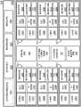
图27图示根据一个实施例的示出针对每种消息类型的所支持的第一级高速缓存属性的表。27 illustrates a table showing the supported first level cache attributes for each message type, according to one embodiment.
图28图示根据一个实施例的示出针对每种消息类型的所支持的多级高速缓存属性的表。Figure 28 illustrates a table showing supported multi-level cache properties for each message type, according to one embodiment.
图29图示根据一个实施例的具有用于控制第一级高速缓存优先级以提高高速缓存效率的示例性操作序列的方法2900。29 illustrates a
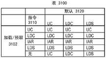
图30图示根据一个实施例的示出针对指令相对于默认高速缓存属性的L1高速缓存优先级的表。30 illustrates a table showing L1 cache priority for instructions relative to default cache attributes, according to one embodiment.
图31图示根据另一实施例的示出针对指令相对于默认高速缓存属性的L1高速缓存优先级的表。31 illustrates a table showing L1 cache priority for instructions relative to default cache attributes, according to another embodiment.
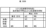
图32图示根据一个实施例的示出针对指令相对于默认L2/L3高速缓存控制的L2/L3高速缓存优先级的表。32 illustrates a table showing L2/L3 cache priority for instructions relative to default L2/L3 cache control, according to one embodiment.
图33图示根据另一实施例的示出针对指令和默认设置相对于PTE设置的L2/L3高速缓存优先级的表。33 illustrates a table showing L2/L3 cache priorities set for instructions and defaults versus PTE settings, according to another embodiment.
图34图示根据一个实施例的用于控制用于共享高速缓存用途的分区方案的流程图3400。34 illustrates a
图35图示根据一个实施例的工作组(或单元组(warp))的数量的变化如何改变传统高速缓存的可用性。Figure 35 illustrates how changes in the number of workgroups (or warps) change the availability of conventional caches, according to one embodiment.
图36A图示根据一个实施例的用于选入硬件高速缓存一致性的流程图。Figure 36A illustrates a flow diagram for opting in to hardware cache coherence, according to one embodiment.
图36B图示根据一个实施例的存储器层级结构。Figure 36B illustrates a memory hierarchy according to one embodiment.
图37A、图37B和图37C图示根据一个实施例的具有用于控制高速缓存操作以提高高速缓存效率的示例性操作序列的方法。37A, 37B, and 37C illustrate a method with an exemplary sequence of operations for controlling cache operations to improve cache efficiency, according to one embodiment.
图38图示具有解耦的控制数据和数据数组的存储器架构3800。38 illustrates a memory architecture 3800 with decoupled control data and data arrays.
图39图示根据一个实施例的用于GPU的基于附加压缩的压缩操作。Figure 39 illustrates an additive compression based compression operation for a GPU, according to one embodiment.
图40图示根据一个实施例的具有用于控制高速缓存操作以提高高速缓存效率的示例性操作序列的方法4000。40 illustrates a
具体实施方式Detailed ways
图形处理单元(GPU)通信地耦合至主机/处理器核以加速例如图形操作、机器学习操作、模式分析操作、和/或各种通用GPU(GPGPU)功能。GPU可通过总线或另一互连(例如,诸如PCIe或NVLink之类的高速互连)通信地耦合至主机处理器/核。替代地,GPU可与核集成在同一封装或芯片上,并且通过内部处理器总线/互连(即,在封装或芯片内部)通信地耦合至核。无论GPU采取何种方式被连接,处理器核都可将工作以工作描述符中所包含的命令/指令序列的形式分配给GPU。GPU随后使用专用电路/逻辑来高效地处理这些命令/指令。A graphics processing unit (GPU) is communicatively coupled to the host/processor core to accelerate, for example, graphics operations, machine learning operations, pattern analysis operations, and/or various general purpose GPU (GPGPU) functions. The GPU may be communicatively coupled to the host processor/core through a bus or another interconnect (eg, a high-speed interconnect such as PCIe or NVLink). Alternatively, the GPU may be integrated on the same package or chip as the core and communicatively coupled to the core through an internal processor bus/interconnect (ie, within the package or chip). Regardless of how the GPUs are connected, the processor cores can distribute work to the GPUs in the form of command/instruction sequences contained in the work descriptors. The GPU then uses dedicated circuitry/logic to efficiently process these commands/instructions.
在以下描述中,陈述了众多特定细节以提供更透彻理解。然而,对于本领域的技术人员将显而易见的是,可以在没有这些特定细节中的一个或多个细节的情况下实践本文中描述的实施例。在其他实例中,未描述公知的特征以免混淆当前实施例的细节。In the following description, numerous specific details are set forth in order to provide a more thorough understanding. It will be apparent, however, to one skilled in the art that the embodiments described herein may be practiced without one or more of these specific details. In other instances, well-known features have not been described so as not to obscure the details of the current embodiments.
系统概览System overview
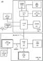
图1是图示出被配置成用于实现本文中所描述的示例性实施例的一个或多个方面的计算系统100的框图。计算系统100包括具有一个或多个处理器102和系统存储器104的处理子系统101,这一个或多个处理器102与系统存储器104经由可包括存储器中枢105的互连路径进行通信。存储器中枢105可以是芯片组组件内的单独组件或者可被集成在一个或多个处理器102内。存储器中枢105经由通信链路106而与I/O子系统111耦合。I/O子系统111包括I/O中枢107,该I/O中枢107可以使得计算系统100能够从一个或多个输入设备108接收输入。另外,I/O中枢107可以使得显示控制器能够向一个或多个显示设备110A提供输出,该显示控制器可包括在一个或多个处理器102中。在一个实施例中,与I/O中枢107耦合的一个或多个显示设备110A可以包括本地的、内部的、或嵌入式的显示设备。1 is a block diagram illustrating a
处理子系统101例如包括经由总线或其他通信链路113耦合至存储器中枢105的一个或多个并行处理器112。通信链路113可以是任何数量的基于标准的通信链路技术或协议中的一种,诸如但不限于PCI Express,或者可以是供应方特定的通信接口或通信结构。一个或多个并行处理器112可形成可包括大量处理核和/或处理集群的集中于计算的并行或向量处理系统,诸如,集成众核(MIC)处理器。例如,一个或多个并行处理器112形成可以向经由I/O中枢107耦合的一个或多个显示设备110A中的一个输出像素的图形处理子系统。一个或多个并行处理器112还可以包括显示控制器以及用于实现到一个或多个显示设备110B的直接连接的显示接口(未示出)。
在I/O子系统111内,系统存储单元114可以连接至I/O中枢107,从而为计算系统100提供存储机制。I/O开关116可被用来提供实现I/O中枢107与其他组件之间的连接的接口机制,这些其他组件诸如,可被集成到平台中的网络适配器118和/或无线网络适配器119、以及可以经由一个或多个插入式设备120被添加的各种其他设备。(多个)插入式设备120还可包括例如一个或多个外部图形处理器设备和/或计算加速器。网络适配器118可以是以太网适配器或另一有线网络适配器。无线网络适配器119可以包括Wi-Fi、蓝牙、近场通信(NFC)或包括一个或多个无线电装置的其他网络设备中的一者或多者。Within I/
计算系统100可以包括未显式地示出的其他组件,包括USB或其他端口连接、光学存储驱动器、视频捕捉设备等等,这些组件也可连接至I/O中枢107。使图1中的各组件互连的通信路径可使用任何合适的协议来实现,这些协议诸如,基于PCI(外围组件互连)的协议(例如,PCI-Express)或任何其他总线或点对点通信接口和/或(多个)协议,诸如NVLink高速互连、或本领域中已知的互连协议。
一个或多个并行处理器112可包含针对图形和视频处理进行优化的电路(包括例如,视频输出电路)并构成图形处理单元(GPU)。替代地或附加地,本文中更详细地描述,一个或多个并行处理器112可包含针对通用处理进行优化同时保留底层计算架构的电路。计算系统100的组件可与一个或多个其他系统元件集成在单个集成电路上。例如,一个或多个并行处理器112、存储器中枢105、处理器102、以及I/O中枢107可以被集成在芯片上系统(SoC)集成电路中。替代地,计算系统100的组件可被集成到单个封装中,以形成系统级封装(SIP)配置。在一个实施例中,计算系统100的组件中的至少部分可被集成到多芯片模块(MCM)中,该多芯片模块可以与其他多芯片模块互连成为模块化计算系统。One or more
将会领会,本文中所示出的计算系统100是说明性的,并且变型和修改是可能的。可按需要修改连接拓扑,包括桥接器的数量和布置、(多个)处理器102的数量、以及(多个)并行处理器112的数量。例如,系统存储器104可直接地而不是通过桥接器连接至(多个)处理器102,而其他设备通过存储器中枢105和(多个)处理器102而与系统存储器104进行通信。在其他替代拓扑中,(多个)并行处理器112连接至I/O中枢107或直接连接至一个或多个处理器102中的一个,而不是连接至存储器中枢105。在其他实施例中,I/O中枢107和存储器中枢105可被集成到单个芯片中。两组或更多组(多个)处理器102经由多个插槽被附连也是可能的,这些处理器102可以与(多个)并行处理器112的两个或更多个实例耦合。It will be appreciated that the
本文中所示出的特定组件中的一些是可选的,并且并非在计算系统100的所有实现方式中都包括这些组件。例如,可支持任何数量的插入式卡或外围设备,或者可消除一些组件。此外,一些架构可针对类似于图1中所图示的那些组件的组件使用不同的术语。例如,在一些架构中,存储器中枢105可被称为北桥,而I/O中枢107可被称为南桥。Some of the specific components shown herein are optional and not included in all implementations of
图2A图示出并行处理器200。并行处理器200可以是如本文中所描述的GPU、GPGPU,等等。并行处理器200的各组件可使用诸如可编程处理器、专用集成电路(ASIC)或现场可编程门阵列(FPGA)之类的一个或多个集成电路设备来实现。所图示的并行处理器200可以是图1所示的(多个)并行处理器112、或图1所示的(多个)并行处理器112中的一个。FIG. 2A illustrates a parallel processor 200 . Parallel processor 200 may be a GPU, GPGPU, etc. as described herein. The components of parallel processor 200 may be implemented using one or more integrated circuit devices, such as programmable processors, application specific integrated circuits (ASICs), or field programmable gate arrays (FPGAs). The illustrated parallel processor 200 may be the parallel processor(s) 112 shown in FIG. 1 , or one of the parallel processor(s) 112 shown in FIG. 1 .
并行处理器200包括并行处理单元202。并行处理单元包括实现与其他设备的通信的I/O单元204,这些其他设备包括并行处理单元202的其他实例。I/O单元204可直接连接至其他设备。例如,I/O单元204通过使用中枢或开关接口(诸如,存储器中枢105)而与其他设备连接。存储器中枢105与I/O单元204之间的连接形成通信链路113。在并行处理单元202内,I/O单元204与主机接口206以及存储器交叉开关216连接,其中,主机接口206接收涉及执行处理操作的命令,并且存储器交叉开关216接收涉及执行存储器操作的命令。Parallel processor 200 includes
当主机接口206经由I/O单元204接收命令缓冲器时,主机接口206可以将用于执行那些命令的工作操作引导至前端208。在一个实施例中,前端208与调度器210耦合,该调度器210被配置成用于将命令或其他工作项目分发给处理集群阵列212。调度器210确保在将任务分发给处理集群阵列212中的处理集群之前处理集群阵列212被恰当地配置并且处于有效状态。可经由在微控制器上执行的固件逻辑来实现调度器210。微控制器实现的调度器210可配置成在粗粒度和细粒度下执行复杂的调度和工作分发操作,从而实现对在处理阵列212上执行的线程的快速抢占和上下文切换。优选地,主机软件可以经由多个图形处理门铃机制中的一者来证实用于在处理阵列212上调度的工作负荷。工作负荷随后可以由调度器微控制器内的调度器210逻辑跨处理阵列212自动地分发。When
处理集群阵列212可以包括高达“N”个处理集群(例如,集群214A、集群214B至集群214N)。处理集群阵列212中的每个集群214A-214N可以执行大量的并发线程。调度器210可以使用各种调度和/或工作分发算法将工作分配给处理集群阵列212中的集群214A-214N,这些调度和/或工作分发算法可取决于针对每种类型的程序或计算出现的工作负荷而变化。调度可以由调度器210动态地处置,或可以在对于被配置成供处理集群阵列212执行的程序逻辑的编译期间部分地由编译器逻辑协助。任选地,处理集群阵列212中的不同的集群214A-214N可以被分配用于处理不同类型的程序或用于执行不同类型的计算。Processing cluster array 212 may include up to "N" processing clusters (eg,
处理集群阵列212可以被配置成用于执行各种类型的并行处理操作。例如,集群阵列212被配置成用于执行通用并行计算操作。例如,处理集群阵列212可以包括用于执行处理任务的逻辑,这些处理任务包括对视频和/或音频数据的过滤、执行建模操作(包括物理操作)以及执行数据变换。The processing cluster array 212 may be configured to perform various types of parallel processing operations. For example, cluster array 212 is configured to perform general purpose parallel computing operations. For example, the processing cluster array 212 may include logic for performing processing tasks including filtering of video and/or audio data, performing modeling operations (including physical operations), and performing data transformations.
处理集群阵列212被配置成用于执行并行图形处理操作。在其中并行处理器200被配置成用于执行图形处理操作的此类实施例中,处理集群阵列212可以包括用于支持此类图形处理操作的执行的附加逻辑,包括但不限于,用于执行纹理操作的纹理采样逻辑以及曲面细分逻辑和其他顶点处理逻辑。另外,处理集群阵列212可以被配置成用于执行与图形处理有关的着色器程序,诸如但不限于,顶点着色器、曲面细分着色器、几何着色器以及像素着色器。并行处理单元202可以经由I/O单元204从系统存储器传输数据以供处理。在处理期间,可在处理期间将所传输的数据存储到芯片上存储器(例如,并行处理器存储器222),随后将该数据写回到系统存储器。The processing cluster array 212 is configured to perform parallel graphics processing operations. In such embodiments in which parallel processor 200 is configured for performing graphics processing operations, processing cluster array 212 may include additional logic for supporting the execution of such graphics processing operations, including but not limited to, for performing Texture sampling logic for texture operations as well as tessellation logic and other vertex processing logic. Additionally, the processing cluster array 212 may be configured to execute shader programs related to graphics processing, such as, but not limited to, vertex shaders, tessellation shaders, geometry shaders, and pixel shaders.
在其中并行处理单元202被用于执行图形处理的实施例中,调度器210可以被配置成用于将处理工作负荷分成近似相等尺寸的任务,以更好地实现图形处理操作到处理集群阵列212中的多个集群214A-214N的分发。在这些实施例中的一些实施例中,处理集群阵列212的部分可以被配置成用于执行不同类型的处理。例如,第一部分可被配置成用于执行顶点着色和拓扑生成,第二部分可被配置成用于执行曲面细分和几何着色,并且第三部分可被配置成用于执行像素着色或其他屏幕空间操作,以产生用于显示的经渲染的图像。由集群214A-214N中的一个或多个集群产生的中间数据可被存储在缓冲器中,以允许该中间数据在集群214A-214N之间传送,以供进行进一步处理。In embodiments in which
在操作期间,处理集群阵列212可以经由调度器210接收将要被执行的处理任务,该调度器210从前端208接收定义处理任务的命令。对于图形处理操作,处理任务可以包括将要被处理的数据以及定义将如何处理该数据(例如,将执行什么程序)的状态参数和命令的索引,该数据例如,表面(补片(patch))数据、基元数据、顶点数据和/或像素数据。调度器210可被配置成用于取出与任务相对应的索引,或者可从前端208接收索引。前端208可以被配置成用于确保在由传入命令缓冲器(例如,批量缓冲器、推入缓冲器等)指定的工作负荷被发起之前处理集群阵列212被配置成有效状态。During operation, the processing cluster array 212 may receive processing tasks to be executed via the scheduler 210, which receives commands from the
并行处理单元202的一个或多个实例中的每个实例可以与并行处理器存储器222耦合。可以经由存储器交叉开关216来访问并行处理器存储器222,该存储器交叉开关216可以接收来自处理集群阵列212以及I/O单元204的存储器请求。存储器交叉开关216可以经由存储器接口218来访问并行处理器存储器222。存储器接口218可以包括多个分区单元(例如,分区单元220A、分区单元220B至分区单元220N),这些分区单元可以各自耦合至并行处理器存储器222的部分(例如,存储器单元)。分区单元220A-220N的数量可被配置成等于存储器单元的数量,以使得第一分区单元220A具有对应的第一存储器单元224A,第二分区单元220B具有对应的存储器单元224B,并且第N分区单元220N具有对应的第N存储器单元224N。在其他实施例中,分区单元220A-220N的数量可以不等于存储器设备的数量。Each of the one or more instances of
存储器单元224A-224N可以包括各种类型的存储器设备,包括动态随机存取存储器(DRAM)或图形随机存取存储器,诸如,同步图形随机存取存储器(SGRAM),包括图形双数据速率(GDDR)存储器。任选地,存储器单元224A-224N还可以包括3D堆叠式存储器,包括但不限于高带宽存储器(HBM)。本领域技术人员将会领会,存储器单元224A-224N的具体实现方式可以有所不同,并且可以从各种常规设计中的一种设计进行选择。诸如帧缓冲器或纹理映射之类的渲染目标可跨存储器单元224A-224N进行存储,从而允许分区单元220A-220N并行地写入每个渲染目标的部分,以高效地使用并行处理器存储器222的可用带宽。在一些实施例中,可排除并行处理器存储器222的本地实例,以有利于利用与本地高速缓存存储器结合的系统存储器的统一存储器设计。
任选地,处理集群阵列212中的集群214A-214N中的任一者有能力处理将被写入到并行处理器存储器222内的存储器单元224A-224N中的任一者的数据。存储器交叉开关216可以被配置成用于将每个集群214A-214N的输出传输到任一分区单元220A-220N或传输到另一集群214A-214N,该另一集群214A-214N可以对该输出执行附加的处理操作。每个集群214A-214N可以通过存储器交叉开关216而与存储器接口218进行通信,以从各种外部存储器设备进行读取或写入到各种外部存储器设备。在具有存储器交叉开关216的实施例中的一个实施例中,存储器交叉开关216具有到存储器接口218的连接以与I/O单元204进行通信,以及具有到并行处理器存储器222的本地实例的连接,从而使得不同处理集群214A-214N内的处理单元能够与系统存储器或对于并行处理单元202而言不是本地的其他存储器通信。一般而言,存储器交叉开关216可以例如能够使用虚拟通道来分离集群214A-214N与分区单元220A-220N之间的业务流(traffic stream)。Optionally, any of the
尽管在并行处理器200内图示出并行处理单元202的单个实例,但可以包括并行处理单元202的任何数量的实例。例如,并行处理单元202的多个实例可以被设置在单个插入式卡上,或者多个插入式卡可以是互连的。并行处理单元202的不同实例可以被配置成用于互操作,即使不同的实例具有不同数量的处理核、不同的本地并行处理器存储器量、和/或其他配置差别。任选地,并行处理单元202的一些实例可以包括相对于其他实例更高精度的浮点单元。包含并行处理单元202或并行处理器200的一个或多个实例的系统能以各种配置和形状因数来实现,这些配置和形状因子包括但不限于,台式计算机、膝上型计算机、或手持式个人计算机、服务器、工作站、游戏控制台和/或嵌入式系统。Although a single instance of
图2B是分区单元220的框图。分区单元220可以是图2A的分区单元220A-220N中的一个分区单元的实例。如所图示,分区单元220包括L2高速缓存221、帧缓冲器接口225、以及ROP 226(栅格操作单元)。L2高速缓存221是被配置成用于执行从存储器交叉开关216和ROP226接收的加载和存储操作的读取/写入高速缓存。读取未命中和紧迫写回请求由L2高速缓存221输出到帧缓冲器接口225以供处理。还可以经由帧缓冲器接口225将更新发送至帧缓冲器以供处理。在一个实施例中,帧缓冲器接口225与并行处理器存储器中的存储器单元中的一者对接,该存储器单元诸如图2A的存储器单元224A-224N(例如,在并行处理器存储器222内)。分期单元220还可附加地或替代地经由存储器控制器(未示出)与并行处理器存储器中的存储器单元中的一个存储器单元对接。FIG. 2B is a block diagram of the
在图形应用中,ROP 226是执行栅格操作(诸如,模板印制(stencil)、z测试、混合等等)的处理单元。ROP 226随后输出经处理的图形数据,经处理的图形数据被存储在图形存储器中。在一些实施例中,ROP 226包括用于压缩被写入至存储器的深度或颜色数据并解压缩从存储器读取的深度或颜色数据的压缩逻辑。压缩逻辑可以是利用多种压缩算法中的一种或多种的无损压缩逻辑。由ROP 226执行的压缩的类型可以基于将要被压缩的数据的统计特性而变化。例如,在一个实施例中,逐片(tile)地对深度和颜色数据执行Δ色彩压缩。In graphics applications,
ROP 226可被包括在每个处理集群(例如,图2A的集群214A-214N)内而非被包括在分区单元220内。在此类实施例中,通过存储器交叉开关216来传送像素数据而非像素片段数据的读取和写入请求。经处理的图形数据可被显示在显示设备(诸如,图1的一个或多个显示设备110中的一个显示设备)上,可被路由以供(多个)处理器102进一步处理,或者可被路由以供图2A的并行处理器200内的处理实体中的一个处理实体进一步处理。
图2C是并行处理单元内的处理集群214的框图。例如,处理集群是图2A的处理集群214A-214N中的一个处理集群的实例。处理集群214可以被配置成用于并行地执行多个线程,其中,术语“线程”是指在特定的输入数据集合上执行的特定程序的实例。任选地,可使用单指令多数据(SIMD)指令发布技术来支持大量线程的并行执行而无需提供多个独立的指令单元。替代地,可使用单指令多线程(SIMT)技术来使用被配置成用于向处理集群中的每个处理集群内的处理引擎集合发布指令的公共指令单元来支持大量总体上同步的线程的并行执行。与其中所有处理引擎典型地执行相同指令的SIMD执行机制不同,SIMT执行允许不同的线程更容易地遵循通过给定的线程程序的发散的执行路径。本领域技术人员将理解,SIMD处理机制表示SIMT处理机制的功能子集。2C is a block diagram of a
可以经由将处理任务分发给SIMT并行处理器的流水线管理器232来控制处理集群214的操作。流水线管理器232从图2A的调度器210接收指令,并且经由图形多处理器234和/或纹理单元236来管理那些指令的执行。所图示的图形多处理器234是SIMT并行处理器的示例性实例。然而,可将不同架构的各种类型的SIMT并行处理器包括在处理集群214内。可以将图形多处理器234的一个或多个实例包括在处理集群214内。图形多处理器234可以处理数据,并且数据交叉开关240可以用于将经处理的数据分发到多个可能的目的地中的一个目的地,包括其他着色器单元。流水线管理器232可以通过为将要经由数据交叉开关240分发的经处理的数据指定目的地来促进对经处理的数据的分发。The operation of the
处理集群214内的每个图形多处理器234可以包括相同的功能执行逻辑集合(例如,算术逻辑单元、加载-存储单元等)。能以流水线化的方式配置功能执行逻辑,在该流水线化的方式中,可以在完成先前指令之前发布新的指令。功能执行逻辑支持各种操作,包括整数和浮点算术、比较操作、布尔操作、位移位、以及各种代数函数的计算。可以利用同一功能单元硬件来执行不同的操作,并且可能存在功能单元的任何组合。Each graphics multiprocessor 234 within
被传送至处理集群214的指令构成线程。跨并行处理引擎集合执行的线程集合是线程组。线程组对不同的输入数据执行同一程序。线程组内的每个线程可以被分派给图形多处理器234内的不同处理引擎。线程组可包括比图形多处理器234内的处理引擎的数量更少的线程。当线程组包括比处理引擎的数量更少的线程时,处理引擎中的一个或多个在处理该线程组所在的周期期间可能是空闲的。线程组也可包括比图形多处理器234内的处理引擎的数量更多的线程。当线程组包括比图形多处理器234内的处理引擎的数量更多的线程时,可在连续的时钟周期上执行处理。任选地,可在图形多处理器234上同时执行多个线程组。Instructions that are passed to the
图形多处理器234可包括内部高速缓存存储器,以执行加载和存储操作。任选地,图形多处理器234可以放弃内部高速缓存并且使用处理集群214内的高速缓存存储器(例如,L1高速缓存248)。每个图形多处理器234还具有对分区单元(例如,图2A的分区单元220A-220N)内的L2高速缓存的访问,这些L2高速缓存在所有处理集群214之间共享并且可被用来在线程之间传输数据。图形多处理器234还可访问芯片外全局存储器,该芯片外全局存储器可以包括本地并行处理器存储器和/或系统存储器中的一者或多者。并行处理单元202外部的任何存储器可被用作全局存储器。其中处理集群214包括图形多处理器234的多个实例的实施例可以共享公共指令和数据,这些公共指令和数据可被存储在L1高速缓存248中。Graphics multiprocessor 234 may include internal cache memory to perform load and store operations. Optionally, graphics multiprocessor 234 may forego internal caches and use cache memory (eg, L1 cache 248 ) within
每个处理集群214可包括被配置成用于将虚拟地址映射到物理地址的MMU 245(存储器管理单元)。在其他实施例中,MMU 245的一个或多个实例可驻留在图2A的存储器接口218内。MMU 245包括用于将虚拟地址映射到片的物理地址的页表条目(PTE)的集合并且可选地包括高速缓存行索引。MMU245可包括可驻留在图形多处理器234或L1高速缓存或处理集群214内的地址转换后备缓冲器(TLB)或高速缓存。对物理地址进行处理,以分发表面数据访问局部性,从而允许分区单元之间的高效的请求交织。可使用高速缓存行索引来确定针对高速缓存行的请求是命中还是未命中。Each
在图形和计算应用中,处理集群214可被配置以使得每个图形多处理器234耦合至纹理单元236以供执行纹理映射操作,例如,确定纹理样本位置、读取纹理数据、以及过滤纹理数据。纹理数据读取自内部纹理L1高速缓存(未示出),或者在一些实施例中,读取自图形多处理器234内的L1高速缓存,并按需要从L2高速缓存、本地并行处理器存储器或系统存储器取出。每个图形多处理器234向数据交叉开关240输出经处理的任务,以向另一处理集群214提供经处理的任务以供进一步处理,或者经由存储器交叉开关216将经处理的任务存储在L2高速缓存、本地并行处理器存储器或系统存储器中。preROP 242(预先栅格操作单元)被配置成用于从图形多处理器234接收数据、将数据引导至ROP单元,这些ROP单元可与如本文中所描述的分区单元(例如,图2A的分区单元220A-220N)一起被定位。preROP 242单元可针对颜色混合执行优化、组织像素颜色数据、并且执行地址转换。In graphics and computing applications, processing
将会领会,本文中所描述的核架构是说明性的,并且变型和修改是可能的。可将任何数量的处理单元(例如,图形多处理器234、纹理单元236、preROP 242等)包括在处理集群214内。进一步地,尽管仅示出了一个处理集群214,但是如本文中所描述的并行处理单元可包括处理集群214的任何数量的实例。任选地,每个处理集群214可以被配置成用于使用单独且不同的处理单元、L1高速缓存等来独立于其他处理集群214进行操作。It will be appreciated that the core architecture described herein is illustrative and that variations and modifications are possible. Any number of processing units (eg,
图2D示出了图形多处理器234的示例,其中图形多处理器234与处理集群214的流水线管理器232耦合。图形多处理器234具有执行流水线,该执行流水线包括但不限于,指令高速缓存252、指令单元254、地址映射单元256、寄存器堆258、一个或多个通用图形处理单元(GPGPU)核262、以及一个或多个加载/存储单元266。GPGPU核262和加载/存储单元266经由存储器和高速缓存互连268而与高速缓存存储器272以及共享存储器270耦合。图形多处理器234可附加地包括张量和/或光线追踪核263,这些张量和/或光线追踪核263包括用于加速矩阵和/或光线追踪操作的硬件逻辑。FIG. 2D shows an example of a
指令高速缓存252可从流水线管理器232接收要执行的指令流。指令被高速缓存在指令高速缓存252中并被分派以供指令单元254执行。指令单元254可以将指令作为线程组(例如,经线)进行分派,其中,线程组中的每个线程被指派给GPGPU核262内的不同执行单元。指令可以通过指定统一地址空间内的地址来访问本地、共享或全局地址空间中的任一者。可以使用地址映射单元256将统一地址空间中的地址转换为可以由加载/存储单元266访问的不同的存储器地址。
寄存器堆258为图形多处理器234的功能单元提供寄存器集合。寄存器堆258为连接至图形多处理器234的功能单元(例如,GPGPU核262、加载/存储单元266)的数据路径的操作数提供临时存储。寄存器堆258可在功能单元中的每个功能单元之间划分,以使得给每个功能单元分配寄存器堆258中的专用部分。例如,寄存器堆258可在由图形多处理器234执行的不同经线之间划分。
GPGPU核262可以各自包括用于执行图形多处理器234的指令的浮点单元(FPU)和/或整数算术逻辑单元(ALU)。在一些实现方式中,GPGPU核262可包括否则会驻留在张量和/或光线追踪核263内的硬件逻辑。GPGPU核262在架构上可能类似,或者可能在架构上相区别。例如,并且在一个实施例中,GPGPU核262的第一部分包括单精度FPU和整数ALU,而GPGPU核的第二部分包括双精度FPU。任选地,FPU可以实现针对浮点算术的IEEE754-2008标准,或实现可变精度浮点算术。图形多处理器234可以附加地包括用于执行特定功能(诸如,复制矩形或像素混合操作)的一个或多个固定功能单元或专门功能单元。GPGPU核中的一个或多个还可以包括固定或专门功能逻辑。The
GPGPU核262可包括能够对多个数据集合执行单个指令的SIMD逻辑。任选地,GPGPU核262可以物理地执行SIMD4、SIMD8和SIMD16指令,并且逻辑地执行SIMD1、SIMD2和SIMD32指令。针对GPGPU核的SIMD指令可以由着色器编译器在编译时生成,或在执行针对单程序多数据(SPMD)或SIMT架构而编写并且编译的程序时自动地生成。可以经由单个SIMD指令来执行被配置成用于SIMT执行模型的程序的多个线程。例如,并且在一个实施例中,可以经由单个SIMD8逻辑单元来并行执行八个SIMT线程,这八个SIMT线程执行相同或类似的操作。The
存储器和高速缓存互连268是将图形多处理器234的功能单元中的每个功能单元连接至寄存器堆258并连接至共享存储器270的互连网络。例如,存储器和高速缓存互连268是允许加载/存储单元266实现共享存储器270与寄存器堆258之间的加载和存储操作的交叉开关互连。寄存器堆258能以与GPGPU核262相同的频率进行操作,因此GPGPU核262与寄存器堆258之间的数据传输是非常低等待时间的。可以使用共享存储器270来实现在图形多处理器234内的功能单元上执行的线程之间的通信。高速缓存存储器272可以被用作数据高速缓存,例如,用于对在功能单元与纹理单元236之间传输的纹理数据进行高速缓存。共享存储器270还可以被用作所高速缓存的受管理的程序。除被存储在高速缓存存储器272内的自动高速缓存的数据之外,在GPGPU核262上执行的线程还能以编程方式将数据存储在共享存储器内。Memory and
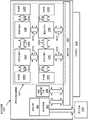
图3A-图3C图示出根据实施例的附加图形多处理器。图3A-图3B图示图形多处理器325、350,它们与图2C的图形多处理器234有关,并且可替代那些图形多处理器中的一个被使用。因此,本文中与图形多处理器234组合的任何特征的公开还公开了与(多个)图形多处理器325、350的对应组合,但是不限于此。图3C图示图形处理单元(GPU)380,该GPU 380包括布置成多核组365A-365N的图形处理资源的专用集合,多核组365A-365N可与图形多处理器325、350对应。所图示的图形多处理器325、350和多核组365A-365N可以是能够同时执行大量执行线程的流式多处理器(SM)。3A-3C illustrate additional graphics multiprocessors, according to an embodiment. Figures 3A-3B illustrate
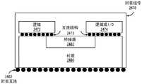
图3A的图形多处理器325包括相对于图2D的图形多处理器234的执行资源单元的多个附加实例。例如,图形多处理器325可以包括指令单元332A-332B、寄存器堆334A-334B和(多个)纹理单元344A-344B的多个实例。图形多处理器325还包括多个图形或计算执行单元集合(例如,GPGPU核336A-336B、张量核337A-337B、光线追踪核338A-338B)以及多个加载/存储单元集合340A-340B。执行资源单元具有公共指令高速缓存330、纹理和/或数据高速缓存存储器342、以及共享存储器346。Graphics multiprocessor 325 of Figure 3A includes additional instances of execution resource units relative to
各组件可以经由互连结构(interconnect fabric)327进行通信。互连结构327可包括一个或多个交叉开关以实现在图形多处理器325的各组件之间的通信。互连结构327可以是单独的、高速网络结构层,图形多处理器325的每个组件堆叠在该网络结构层上。图形多处理器325的组件经由互连结构327与远程组件进行通信。例如,GPGPU核336A-336B、337A-337B以及338A-338B可以各自经由互连结构327与共享存储器346通信。互连结构327可以对图形多处理器325内的通信进行仲裁,以确保组件之间公平的带宽分配。Components may communicate via
图3B的图形处理器350包括多个执行资源集合356A-356D,其中,如图2D和图3A中所图示,每个执行资源集合包括多个指令单元、寄存器堆、GPGPU核、以及加载存储单元。执行资源356A-356D可以与用于纹理操作的(多个)纹理单元360A-360D协同工作,同时共享指令高速缓存354和共享存储器353。例如,执行资源356A-356D可以共享指令高速缓存354和共享存储器353以及纹理和/或数据高速缓存存储器358A-358B的多个实例。各组件可以经由类似于图3A的互连结构327的互连结构352进行通信。The graphics processor 350 of Figure 3B includes multiple sets of
本领域技术人员将会理解,图1、图2A-图2D以及图3A-图3B中所描述的架构是描述性的并且不限制本实施例的范围。因此,在不背离本文中所描述的实施例的范围的情况下,本文中所描述的技术可在任何恰当配置的处理单元上实现,该处理单元包括但不限于一个或多个移动应用处理器、一个或多个台式机或服务器中央处理单元(CPU)(包括多核CPU)、一个或多个并行处理单元(诸如,图2A的并行处理单元202)、以及一个或多个图形处理器或专用处理单元。Those skilled in the art will appreciate that the architectures described in FIGS. 1 , 2A-2D, and 3A-3B are descriptive and do not limit the scope of the present embodiments. Accordingly, the techniques described herein may be implemented on any suitably configured processing unit, including but not limited to one or more mobile application processors, without departing from the scope of the embodiments described herein. , one or more desktop or server central processing units (CPUs) (including multi-core CPUs), one or more parallel processing units (such as
本文中所描述的并行处理器或GPGPU可通信地耦合至主机/处理器核以加速图形操作、机器学习操作、模式分析操作、以及各种通用GPU(GPGPU)功能。GPU可通过总线或其他互连(例如,诸如PCIe或NVLink之类的高速互连)而通信地耦合至主机处理器/核。在其他实施例中,GPU可与核集成在同一封装或芯片上,并且通过内部处理器总线/互连(即,在封装或芯片内部)通信地耦合至核。不论连接GPU所采用的方式如何,处理器核都可以采用工作描述符中所包含的命令/指令序列的形式将工作分配给GPU。GPU随后使用专用电路/逻辑来有效地处理这些命令/指令。The parallel processors or GPGPUs described herein are communicatively coupled to host/processor cores to accelerate graphics operations, machine learning operations, pattern analysis operations, and various general purpose GPU (GPGPU) functions. The GPU may be communicatively coupled to the host processor/core through a bus or other interconnect (eg, a high-speed interconnect such as PCIe or NVLink). In other embodiments, the GPU may be integrated on the same package or chip as the core and communicatively coupled to the core through an internal processor bus/interconnect (ie, within the package or chip). Regardless of the way in which the GPU is connected, the processor core can assign work to the GPU in the form of a sequence of commands/instructions contained in the work descriptor. The GPU then uses dedicated circuitry/logic to efficiently process these commands/instructions.
图3C图示图形处理单元(GPU)380,该GPU 380包括布置为多核组365A-365N的专用的图形处理资源的集合。虽然提供仅单个多核组365A的细节,但是将理解,其他多核组365B-365N可配备有相同或类似集合的图形处理资源。参照多核组365A-365N描述的细节也适用于本文中描述的任何图形多处理器234、325、350。3C illustrates a graphics processing unit (GPU) 380 that includes a collection of dedicated graphics processing resources arranged as multi-core groups 365A-365N. While details of only a single multi-core group 365A are provided, it will be appreciated that other
如所图示,多核组365A可包括图形核的集合370、张量核的集合371以及光线追踪核的集合372。调度器/分派器368调度和分派图形线程用于在各个核370、371、372上执行。寄存器堆的集合369存储在执行图形线程时由核370、371、372使用的操作数值。这些寄存器堆可包括例如用于存储整数值的整数寄存器、用于存储浮点值的浮点寄存器、用于存储紧缩数据元素(整数和/或浮点数据元素)的向量寄存器以及用于存储张量/矩阵值的操作数矩阵寄存器。操作数矩阵寄存器可被实现为组合的向量寄存器的集合。As illustrated, the multi-core group 365A may include a
一个或多个组合的第一级(L1)高速缓存和共享存储器单元373在本地将图形数据存储在每个多核组365A内,图形数据诸如纹理数据、顶点数据、像素数据、光线数据、包围体数据等。一个或多个纹理单元374也可用于执行纹理操作,诸如,纹理映射和采样。由所有多核组365A-365N或多核组365A-365N的子集共享的第二级(L2)高速缓存375存储用于多个并发的图形线程的图形数据和/或指令。如所图示,可跨多个多核组365A-365N共享L2高速缓存375。一个或多个存储器控制器367将GPU 380耦合至存储器366,该存储器366可以是系统存储器(例如,DRAM)和/或专用图形存储器(例如,GDDR6存储器)。One or more combined first level (L1) cache and shared
输入/输出(I/O)电路363将GPU 380耦合至一个或多个I/O设备362,这一个或多个I/O设备362诸如数字信号处理器(DSP)、网络控制器或用户输入设备。芯片上互连可用于将I/O设备362耦合至GPU 380和存储器366。I/O电路363的一个或多个存储器管理单元(IOMMU)364直接将I/O设备362耦合至系统存储器366。任选地,IOMMU 364管理用于将虚拟地址映射到系统存储器366中的物理地址的多个集合的页表。I/O设备362、(多个)CPU 361和(多个)GPU 380随后可共享相同的虚拟地址空间。Input/output (I/O)
在IOMMU 364的一个实现方式中,IOMMU 364支持虚拟化。在这种情况下,IOMMU364管理用于将宾客/图形虚拟地址映射到宾客/图形物理地址的第一集合的页表以及用于将宾客/图形物理地址映射到(例如,系统存储器366内的)系统/主机物理地址的第二集合的页表。第一集合的页表和第二集合的页表中的每一个的基址可被存储在控制寄存器中,并且在上下文切换时被换出(例如,使得新上下文被提供有对相关集合的页表的访问权)。虽然未在图3C中图示,但是核370、371、372和/或多核组365A-365N中的每一个可包括转换后备缓冲器(TLB),这些TLB用于对宾客虚拟至宾客物理转换、宾客物理至主机物理转换以及宾客虚拟至主机物理转换进行高速缓存。In one implementation of the
CPU 361、GPU 380和I/O设备362可被集成在单个半导体芯片和/或芯片封装上。所图示的存储器366可集成在同一芯片上,或者可经由片外接口被耦合至存储器控制器367。在一个实现方式中,存储器366包括与其他物理系统级存储器共享同一虚拟地址空间的GDDR6存储器,但是本文中描述的根本性原理不限于该特定的实现方式。
张量核371可包括专门设计成用于执行矩阵操作的多个执行单元,这些矩阵操作是用于执行深度学习操作的基本计算操作。例如,可将同步矩阵乘法操作用于神经网络训练和推断。张量核371可使用各种操作数精度来执行矩阵处理,操作数精度包括单精度浮点(例如,32位)、半精度浮点(例如,16位)、整数字(16位)、字节(8位)和半字节(4位)。例如,神经网络实现方式提取每个经渲染场景的特征,从而潜在地组合来自多个帧的细节,以构建高质量的最终图像。
在深度学习实现方式中,可调度并行的矩阵乘法工作用于在张量核371上执行。神经网络的训练尤其需要大量矩阵点积操作。为了处理N xN x N矩阵乘法的内积公式化,张量核371可包括至少N个点积处理元件。在矩阵乘法开始之前,一个完整的矩阵被加载到操作数矩阵寄存器中,并且对于N个循环中的每个循环,第二矩阵的至少一列被加载。对于每个循环,存在被处理的N个点积。In a deep learning implementation, parallel matrix multiplication jobs can be scheduled for execution on
取决于特定的实现方式,能以不同精度来存储矩阵元素,包括16位的字、8位的字节(例如,INT8)以及4位的半字节(例如,INT4)。可为张量核371指定不同的精度模式以确保将最高效的精度用于不同的工作负载(例如,诸如推断工作负载,其可容忍至字节和半字节的离散化(quantization))。Depending on the particular implementation, matrix elements can be stored with different precisions, including 16-bit words, 8-bit bytes (eg, INT8), and 4-bit nibbles (eg, INT4). Different precision modes may be specified for
光线追踪核372可加速用于实时光线追踪实现方式和非实时光线追踪实现方式两者的光线追踪操作。具体而言,光线追踪核372可包括光线遍历/相交电路,该光线遍历/相交电路用于使用包围体层级结构(BVH)来执行光线遍历并识别封围在BVH容体内的光线与基元之间的相交。光线追踪核372还可包括用于执行深度测试和剔除(例如,使用Z缓冲器或类似布置)的电路。在一个实现方式中,光线追踪核372与本文中描述的图像降噪技术一致地执行遍历和相交操作,该图像降噪技术的至少部分可在张量核371上执行。例如,量核371可实现深度学习神经网络以执行对由光线追踪核372生成的帧的降噪。然而,(多个)CPU361、图形核370和/或光线追踪核372还可实现降噪和/或深度学习算法的全部或部分。
此外,如上文所描述,可采用对于降噪的分布式方法,在该分布式方法中,GPU 380在通过网络或高速互连而耦合至其他计算设备的计算设备中。在该分布式方式中,经互连的计算设备可共享神经网络学习/训练数据以改善整个系统学习执行用于不同类型的图像帧和/或不同的图形应用的降噪的速度。Furthermore, as described above, a distributed approach to noise reduction may be employed in which
光线追踪核372可处理所有的BVH遍历和/或光线-基元相交,从而挽救图形核370免于被针对每条光线的数千条指令过载。例如,每个光线追踪核372包括用于执行包围盒测试(例如,用于遍历操作)的第一集合的专业电路和/或用于执行光线-三角形相交测试(例如,使已被遍历的光线相交)的第二集合的专业电路。由此,例如,多核组365A可简单地发起光线探测,并且光线追踪核372独立地执行光线遍历和相交,并将命中数据(例如,命中、无命中、多个命中等)返回到线程上下文。当光线追踪核370执行遍历和相交操作时,其他核371、372被释放以执行其他图形或计算工作。
任选地,每个光线追踪核372可包括用于执行BVH测试操作的遍历单元和/或执行光线-基元相交测试的相交单元。相交单元生成“命中”、“无命中”或“多个命中”响应,该相交单元将这些响应提供给适当的线程。在遍历和相交操作期间,其他核(例如,图形核370和张量核371)的执行资源被释放以执行其他形式的图形工作。Optionally, each
在下文描述的一个任选实施例中,使用在其中工作被分布在图形核370与光线追踪核372之间的混合式栅格化/光线追踪方法。In an optional embodiment described below, a hybrid rasterization/ray tracing approach is used in which work is distributed between
光线追踪核372(和/或其他核370、371)可包括对光线追踪指令集的硬件支持,光线追踪指令集诸如:微软的DirectX光线追踪(DXR),其包括DispatchRays命令;以及光线生成着色器、最近命中着色器、任何命中着色器和未命中着色器,它们启用为每个对象指派唯一集合的着色器和纹理。可由光线追踪核372、图形核370和张量核371支持的另一光线追踪平台是Vulkan 1.1.85。然而,要注意本文中描述的根本性原理不限于任何特定的光线追踪指令集架构ISA。Ray tracing core 372 (and/or
一般而言,各个核372、371、370可支持包括用于以下一项或多项的指令/函数的光线追踪指令集:光线生成、最近命中、任何命中、光线-基元相交、逐基元和层级结构包围盒构建、未命中、拜访、和异常。更具体地,优选实施例包括用于执行以下功能中的一项或多项的光线追踪指令:In general, each core 372, 371, 370 may support a ray tracing instruction set including instructions/functions for one or more of the following: ray generation, nearest hit, any hit, ray-primitive intersection, per-primitive and hierarchical bounding box builds, misses, calls, and exceptions. More specifically, preferred embodiments include ray tracing instructions for performing one or more of the following functions:
光线生成——可为每个像素、样本或用户定义的工作分配执行光线生成指令。Ray Generation - Ray generation instructions can be executed for each pixel, sample or user-defined assignment.
最近命中——可执行最近命中指令以对场景内光线与基元的最近交点定位。Nearest Hit - The nearest hit command can be executed to locate the closest intersection of rays and primitives within the scene.
任何命中——任何命中指令识别场景内光线与基元的多个相交,从而潜在地识别新的最近交点。Any Hit - Any Hit instruction identifies multiple intersections of rays and primitives within the scene, potentially identifying new closest intersections.
相交——相交指令执行光线-基元相交测试并输出结果。Intersect - The Intersect instruction performs a ray-primitive intersection test and outputs the result.
逐基元包围盒构建——该指令围绕给定的基元或基元组建立包围盒(例如,当建立新BVH或其他加速数据结构时)。Primitive-by-Primitive Bounding Box Build - This instruction builds a bounding box around a given primitive or group of primitives (eg, when building a new BVH or other accelerated data structure).
未命中——指示光线未命中场景或场景的指定区域内的全部几何体。Missed - Indicates that the ray missed the scene or all geometry within a specified area of the scene.
拜访——指示光线将遍历的子容体。Visit - Indicates the subvolume that the ray will traverse.
异常——包括各种类型的异常处置器(例如,为各种错误条件调用)。Exceptions - includes various types of exception handlers (eg, invoked for various error conditions).
用于GPU到主机处理器互连的技术Technology for GPU-to-Host Processor Interconnect
图4A图示出其中多个GPU 410-413(例如,诸如图2A中示出的并行处理器200)通过高速链路440A-440D(例如,总线、点对点互连等)通信地耦合至多个多核处理器405-406的示例性架构。取决于实现方式,高速链路440A-440D可支持4GB/s、30GB/s、80GB/s或更高的通信吞吐量。可使用各种互连协议,这些互连协议包括但不限于,PCIe 4.0或5.0以及NVLink 2.0。然而,本文中描述的基本原理不限于任何特定的通信协议或吞吐量。4A illustrates where multiple GPUs 410-413 (eg, such as parallel processor 200 shown in FIG. 2A) are communicatively coupled to multiple multi-cores through high-
GPU 410-413中的两个或更多个可通过高速链路442A-442B进行互连,这可使用与用于高速链路440A-440D的那些协议/链路相同或不同的协议/链路来实现。类似地,多核处理器405-406中的两个或更多个可通过高速链路443进行连接,该高速链路443可以是在20GB/s、30GB/s、120GB/s或更高速度下进行操作的对称多处理器(SMP)总线。替代地,图4A中示出的各种系统组件之间的所有通信可使用相同的协议/链路(例如,通过公共互连结构)来完成。如所提到,然而,本文中描述的基本原理不限于任何特定类型的互连技术。Two or more of GPUs 410-413 may be interconnected by high-
每个多核处理器405-406可分别经由存储器互连430A-430B通信地耦合至处理器存储器401-402,并且每个GPU 410-413分别通过GPU存储器互连450A-450D通信地耦合至GPU存储器420-423。存储器互连430A-430B和450A-450D可利用相同或不同的存储器访问技术。作为示例并且不作为限制,处理器存储器401-402和GPU存储器420-423可以是诸如动态随机存取存储器(DRAM)(包括堆叠的DRAM)、图形DDR SDRAM(GDDR)(例如,GDDR5、GDDR6)、或高带宽存储器(HBM)之类的易失性存储器,并且/或者可以是诸如3D Xpoint或Nano-Ram之类的非易失性存储器。例如,这些存储器中的某个部分可以是易失性存储器并且另一部分可以是非易失性存储器(例如,使用两级存储器(2LM)层级结构)。Each multi-core processor 405-406 may be communicatively coupled to processor memory 401-402 via memory interconnects 430A-430B, respectively, and each GPU 410-413 may be communicatively coupled to GPU memory via GPU memory interconnects 450A-450D, respectively 420-423. Memory interconnects 430A-430B and 450A-450D may utilize the same or different memory access techniques. By way of example and not limitation, processor memory 401-402 and GPU memory 420-423 may be, for example, dynamic random access memory (DRAM) (including stacked DRAM), graphics DDR SDRAM (GDDR) (eg, GDDR5, GDDR6) , or volatile memory such as High Bandwidth Memory (HBM), and/or may be non-volatile memory such as 3D Xpoint or Nano-Ram. For example, some of these memories may be volatile memory and another portion may be non-volatile memory (eg, using a two-level memory (2LM) hierarchy).
如下文中所描述,尽管各处理器405-406和GPU 410-413可分别物理地耦合至特定的存储器401-402、420-423,但是可实现其中同一虚拟系统地址空间(也被称为“有效地址”空间)在所有的各种物理存储器之间进行分布的统一存储器架构。例如,处理器存储器401-402可各自包括64GB的系统存储器地址空间,并且GPU存储器420-423可各自包括32GB的系统存储器地址空间(在该示例中,得到总计256GB可寻址的存储器)。As described below, although each of the processors 405-406 and GPUs 410-413 may be physically coupled to specific memories 401-402, 420-423, respectively, the same virtual system address space (also referred to as "effective" Address "space") is a unified memory architecture that is distributed among all the various physical memories. For example, processor memory 401-402 may each include 64GB of system memory address space, and GPU memory 420-423 may each include 32GB of system memory address space (resulting in a total of 256GB of addressable memory in this example).
图4B图示出多核处理器407和图形加速模块446之间的互连的附加任选细节。图形加速模块446可包括集成在线卡上的一个或多个GPU芯片,该线卡经由高速链路440耦合至处理器407。替代地,可将图形加速模块446集成在与处理器407相同的封装或芯片上。FIG. 4B illustrates additional optional details of the interconnection between
所图示的处理器407包括多个核460A-460D,各自具有转换后备缓冲器461A-461D以及一个或多个高速缓存462A-462D。核可包括用于执行指令并处理数据的各种其他组件,未图示出这些组件以避免使本文中描述的组件(例如,指令取出单元、分支预测单元、解码器、执行单元、重排序缓冲器等)的基本原理模糊。高速缓存462A-462D可包括第1级(L1)高速缓存和第2级(L2)高速缓存。另外,一个或多个共享高速缓存456可被包括在高速缓存层级结构中并由核集合460A-460D共享。例如,处理器407的一个实施例包括24个核,各自具有其自己的L1高速缓存、十二个共享L2高速缓存、以及十二个共享L3高速缓存。在该实施例中,L2高速缓存和L3高速缓存中的一者由两个相邻的核共享。处理器407和图形加速器集成模块446与系统存储器441连接,该系统存储器441可包括处理器存储器401-402。The illustrated
经由通过一致性总线464的核间通信为存储在各高速缓存462A-462D、456和系统存储器441中的数据和指令维持一致性。例如,每个高速缓存可具有与其相关联的高速缓存一致性逻辑/电路,以响应于检测到的对特定高速缓存行的读取或写入而通过一致性总线464进行通信。在一种实现方式中,通过一致性总线464实现高速缓存监听协议,以监听高速缓存访问。高速缓存监听/一致性技术为本领域技术人员很好地理解并且将不在此详细描述,以避免使本文中描述的基本原理模糊。Coherency is maintained for data and instructions stored in
可提供代理电路425,该代理电路425将图形加速模块446通信地耦合至一致性总线464,从而允许图形加速模块446作为核的对等体参与高速缓存一致性协议。具体而言,接口435通过高速链路440(例如,PCIe总线、NVLink等)提供到代理电路425的连接性,并且接口437将图形加速模块446连接至高速链路440。A
在一种实现方式中,加速器集成电路436代表图形加速模块446的多个图形处理引擎431、432、N提供高速缓存管理、存储器访问、上下文管理、以及中断管理服务。图形处理引擎431、432、N可各自包括单独的图形处理单元(GPU)。替代地,图形处理引擎431、432、N可包括GPU内的不同类型的图形处理引擎,诸如,图形执行单元、媒体处理引擎(例如,视频编码器/解码器)、采样器以及blit引擎。换言之,图形加速模块可以是具有多个图形处理引擎431-432、N的GPU,或者图形处理引擎431-432、N可以是集成在公共封装、线卡或芯片上的单独的GPU。In one implementation, the accelerator integrated
加速器集成电路436可包括存储器管理单元(MMU)439,该MMU439用于执行诸如虚拟到物理存储器转换(也称为有效到实际存储器转换)之类的各种存储器管理功能以及用于访问系统存储器441的存储器访问协议。MMU 439还可包括用于对虚拟/有效到物理/实际地址转换进行高速缓存的转换后备缓冲器(TLB)(未示出)。在一种实现方式中,高速缓存438存储用于由图形处理引擎431-432、N高效访问的命令和数据。使高速缓存438和图形存储器433-434、M中存储的数据可与核高速缓存462A-462D、456以及系统存储器441保持一致。如所提到,这可经由代理电路425来完成,该代理电路425代表高速缓存438和存储器433-434、M参与高速缓存一致性机制(例如,向高速缓存438发送与处理器高速缓存462A-462D、456上的高速缓存行的修改/访问相关的更新并从高速缓存438接收更新)。The accelerator integrated
寄存器集合445存储针对由图形处理引擎431-432、N执行的线程的上下文数据,并且上下文管理电路448管理这些线程上下文。例如,上下文管理电路448可在上下文切换期间执行用于保存和恢复各线程的上下文的保存和恢复操作(例如,其中,第一线程被保存并且第二线程被保存,以使得第二线程可以由图形处理引擎执行)。例如,在上下文切换时,上下文管理电路448可将当前寄存器值存储到存储器中的指定区域(例如,由上下文指针标识)。当返回到该上下文时,其随后可恢复寄存器值。中断管理电路447例如可接收并处理接收自系统设备的中断。Register set 445 stores context data for threads executed by graphics processing engines 431-432, N, and
在一种实现方式中,由MMU 439将来自图形处理引擎431的虚拟/有效地址转换为系统存储器441中的实际/物理地址。任选地,加速器集成电路436支持多个(例如,4个、8个、16个)图形加速器模块446和/或其他加速器设备。图形加速器模块446可专用于在处理器407上执行的单个应用,或者可在多个应用之间共享。任选地,提供虚拟化图形执行环境,其中,图形处理引擎431-432、N的资源与多个应用、或虚拟机(VM)共享。这些资源可被细分为“切片(slice)”,这些切片基于处理要求以及与VM和/或应用相关联的优先级而被分配给不同的VM和/或应用。In one implementation, virtual/effective addresses from
因此,加速器集成电路436充当用于图形加速模块446的到系统的桥接器,并且提供地址转换和系统存储器高速缓存服务。在一个实施例中,为促进桥接功能,加速器集成电路436还可包括用于启用对电压、时钟计时、性能、热和安全的系统控制的共享I/O 497(例如,PCIe、USB)和硬件。共享I/O 497可利用分开的物理连接,或者可跨越高速链路440。另外,加速器集成电路436可为主机处理器提供虚拟化设施,以管理对图形处理引擎、中断和存储器管理的虚拟化。Thus, accelerator integrated
因为图形处理引擎431-432、N的硬件资源被显式地映射到由主机处理器407查看的实际地址空间,所以任何主机处理器可以使用有效地址值直接对这些资源进行寻址。加速器集成电路436的一个任选功能是对图形处理引擎431-432、N的物理分离,以使得它们对系统看起来是独立单元。Because the hardware resources of graphics processing engines 431-432, N are explicitly mapped into the actual address space viewed by
一个或多个图形存储器433-434、M可分别耦合至图形处理引擎431-432、N中的每个图形处理引擎。图形存储器433-434、M存储由图形处理引擎431-432、N中的每个图形处理引擎处理的指令和数据。图形存储器433-434、M可以是诸如DRAM(包括堆叠的DRAM)、GDDR存储器(例如,GDDR5、GDDR6)或HBM之类的易失性存储器,和/或可以是诸如3D XPoint或Nano-Ram之类的非易失性存储器。One or more graphics memories 433-434, M may be coupled to each of the graphics processing engines 431-432, N, respectively. Graphics memories 433-434, M store instructions and data processed by each of graphics processing engines 431-432, N. Graphics memory 433-434, M may be volatile memory such as DRAM (including stacked DRAM), GDDR memory (eg, GDDR5, GDDR6) or HBM, and/or may be such as 3D XPoint or Nano-Ram class of non-volatile memory.
为了降低高速链路440上的数据通信量,可使用偏置技术来确保存储在图形存储器433-434、M中的数据是将由图形处理引擎431-432、N最频繁地使用并且优选地不由核460A-460D使用(至少不频繁地使用)的数据。类似地,偏置机制尝试将核(并且优选地,不是图形处理引擎431-432、N)所需要的数据保持在这些核的高速缓存462A-462D、456和系统存储器411内。To reduce data traffic on
根据图4C中示出的变体,加速器集成电路436被集成在处理器407内。经由接口437和接口435(其同样可利用任何形式的总线或接口协议),图形处理引擎431-432、N通过高速链路440与加速器集成电路436直接通信。加速器集成电路436可执行与参考图4B所描述的那些操作相同的操作,但是考虑到该加速器集成电路436与一致性总线464和高速缓存462A-462D、456紧密邻近,其潜在地可在较高的吞吐量下执行操作。According to the variant shown in FIG. 4C , the accelerator integrated
所描述的实施例可支持不同的编程模型,这些编程模型包括专用进程编程模型(无图形加速模块虚拟化)和共享编程模型(具有虚拟化)。后者可包括受加速器集成电路436控制的编程模型以及受图形加速模块446控制的编程模型。The described embodiments may support different programming models including a dedicated process programming model (without graphics acceleration module virtualization) and a shared programming model (with virtualization). The latter may include a programming model controlled by accelerator integrated
在专用进程模型的实施例中,图形处理引擎431-432、N可在单个操作系统下专用于单个应用或进程。该单个应用可以将其他应用请求汇集至图形引擎431-432、N,从而提供VM/分区内的虚拟化。In embodiments of the dedicated process model, the graphics processing engines 431-432, N may be dedicated to a single application or process under a single operating system. This single application can funnel other application requests to the graphics engine 431-432, N, thereby providing virtualization within the VM/partition.
在专用进程编程模型中,图形处理引擎431-432、N可由多个VM/应用分区共享。共享模型要求系统管理程序使图形处理引擎431-432、N虚拟化,以允许由每个操作系统访问。对于不具有管理程序的单分区系统,图形处理引擎431-432、N由操作系统所有。在这两种情况下,操作系统可以使图形处理引擎431-432、N虚拟化,以提供对每个进程或应用的访问。In a dedicated process programming model, graphics processing engines 431-432, N may be shared by multiple VM/application partitions. The shared model requires the hypervisor to virtualize the graphics processing engines 431-432, N to allow access by each operating system. For a single partition system without a hypervisor, the graphics processing engines 431-432, N are owned by the operating system. In both cases, the operating system may virtualize the graphics processing engines 431-432, N, to provide access to each process or application.
对于共享编程模型,图形加速模块446或各个图形处理引擎431-432、N使用进程句柄来选择进程要素。进程要素可被存储在系统存储器441中,并且可以是使用本文中所描述的有效地址到实际地址转换技术可寻址的。进程句柄可以是在向图形处理引擎431-432、N注册其上下文(即,调用系统软件以将进程要素添加到进程要素链表)时提供给主机进程的实现方式特定的值。进程句柄的较低的16位可以是进程要素在进程要素链表内的偏移。For the shared programming model, the
图4D图示出示例性加速器集成切片490。如本文中所使用,“切片”包括加速器集成电路436的处理资源的指定部分。系统存储器441内的应用有效地址空间482存储进程要素483。进程要素483可响应于来自在处理器407上执行的应用480的GPU调用481而被存储。进程要素483包含对应应用480的进程状态。包含在进程要素483中的工作描述符(WD)484可以是由应用请求的单个作业,或者可包含指向作业队列的指针。在后一种情况中,WD 484是指向应用的地址空间482中的作业请求队列的指针。FIG. 4D illustrates an exemplary accelerator integrated
图形加速模块446和/或各个图形处理引擎431-432、N可以由系统中的进程的全部或其子集共享。例如,本文中描述的技术可用于建立进程状态并将WD 484发送至图形加速模块446以在虚拟化环境中开始作业的基础设施。The
在一种实现方式中,专用进程编程模型是实现方式特定的。在该模型中,单个进程拥有图形加速模块446或单独的图形处理引擎431。因为图形加速模块446为单个进程所拥有,所以在指派图形加速模块446时,管理程序针对拥有的分区对加速器集成电路436进行初始化,并且操作系统针对拥有的进程对加速器集成电路436进行初始化。In one implementation, the dedicated process programming model is implementation specific. In this model, a single process owns a
在操作中,加速器集成切片490中的WD取出单元491取出包括对将要由图形加速模块446的图形处理引擎中的一个完成的工作的指示的下一WD 484。如所图示,来自WD 484的数据可被存储在寄存器445中,并且由MMU 439、中断管理电路447和/或上下文管理电路448使用。例如,MMU 439可包括用于访问OS虚拟地址空间485内的段表/页表486的段/页走查电路。中断管理电路447可处理从图形加速模块446接收的中断事件492。当执行图形操作时,由图形处理引擎431-432、N生成的有效地址493由MMU 439转换成实际地址。In operation, the WD fetch
相同的寄存器集合445可针对每个图形处理引擎431-432、N和/或图形加速模块446被复制并且可由管理程序或操作系统初始化。这些复制的寄存器中的每一个可被包括在加速器集成切片490中。在表1中示出可由管理程序初始化的示例性寄存器。The same set of
表1-管理程序初始化的寄存器Table 1 - Registers initialized by the hypervisor
在表2中示出可由操作系统初始化的示例性寄存器。Exemplary registers that can be initialized by the operating system are shown in Table 2.
表2-操作系统初始化的寄存器Table 2 - Registers initialized by the operating system


每个WD 484对于特定的图形加速模块446和/或图形处理引擎431-432、N可以是特定的。其包含图形处理引擎431-432、N进行其工作所要求的所有信息,或者其可以是指向应用已经建立将要完成的工作的命令队列所在的存储器位置的指针。Each
图4E图示出共享模型的附加任选细节。它包括进程要素列表499被存储在其中的管理程序实际地址空间498。管理程序实际地址空间498是经由管理程序496可访问的,该管理程序496使用于操作系统495的图形加速模块引擎虚拟化。Figure 4E illustrates additional optional details of the shared model. It includes the hypervisor
共享编程模型允许来自系统中的分区的全部或其子集的进程的全部或其子集使用图形加速模块446。存在其中图形加速模块446由多个进程和分区共享的两种编程模型:时分共享和图形定向共享。The shared programming model allows all or a subset of processes from all or a subset of partitions in the system to use the
在该模型中,系统管理程序496拥有图形加速模块446并使其功能对所有的操作系统495可用。为了使图形加速模块446支持由系统管理程序496进行的虚拟化,图形加速模块446可遵守下列要求:1)应用的作业请求必须是自主的(即,不需要在作业之间维持状态),或者图形加速模块446必须提供上下文保存和恢复机制。2)由图形加速模块446保证在所指定的时间量内完成应用的作业请求,包括任何转换错误,或者图形加速模块446提供抢占对作业的处理的能力。3)当在定向共享编程模型下进行操作时,必须保证图形加速模块446在进程之间的公平性。In this model,
对于共享模型,可要求应用480利用图形加速模块446类型、工作描述符(WD)、权限掩码寄存器(AMR)值和上下文保存/恢复区域指针(CSRP)作出操作系统495系统调用。图形加速模块446类型描述系统调用的目标加速功能。图形加速模块446类型可以是系统特定的值。特别针对图形加速模块446对WD进行格式化,并且WD可以采用图形加速模块446命令、指向用户定义的结构的有效地址指针、指向命令队列的有效地址指针、或用于描述将要由图形加速模块446完成的工作的任何其他数据结构的形式。在一个实施例中,AMR值是用于当前进程的AMR状态。传递至操作系统的值类似于设置AMR的应用。如果加速器集成电路436和图形加速模块446实现方式不支持用户权限掩码覆盖寄存器(UAMOR),则操作系统可在管理程序调用中传递AMR之前将当前UAMOR值应用到AMR值。管理程序496可在将AMR放置到进程要素483中之前可选地应用当前权限掩码覆盖寄存器(AMOR)值。CSRP可以是寄存器445中的包含应用地址空间482中用于图形加速模块446保存和恢复上下文状态的区域的有效地址的一个寄存器。如果不要求在作业之间对状态进行保存或者在作业被抢占时,则该指针是可选的。上下文保存/恢复区域可以是固定的系统存储器。For the shared model, application 480 may be required to make
一旦接收系统调用,则操作系统495可验证应用480已注册并且已给予该应用480使用图形加速模块446的权限。操作系统495随后利用表3中示出的信息来调用管理程序496。Once the system call is received, the
表3-OS对管理程序的调用参数Table 3-OS calls parameters to the hypervisor
一旦接收管理程序调用,则管理程序496验证操作系统495已注册并且已给予该操作系统495使用图形加速模块446的权限。管理程序496随后将进程要素483置于针对对应的图形加速模块446类型的进程要素链表中。进程要素可包括表4中示出的信息。Once the hypervisor call is received, the
表4-进程要素信息Table 4 - Process Element Information


管理程序可使多个加速器集成切片490寄存器445初始化。The hypervisor may initialize the multiple
如图4F中所图示,在一个任选实现方式中,采用经由公共虚拟存储器地址空间可寻址的统一存储器,该公共虚拟存储器地址空间被用来访问物理处理器存储器401-402和GPU存储器420-423。在该实现方式中,在GPU410-413上执行的操作利用同一虚拟/有效存储器地址空间来访问处理器存储器401-402并且反之亦然,由此简化可编程性。虚拟/有效地址空间的第一部分可被分配给处理器存储器401,第二部分被分配给第二处理器存储器402,第三部分被分配给GPU存储器420,依此类推。整个虚拟/有效存储器空间(有时被称为有效地址空间)由此可跨处理器存储器401-402和GPU存储器420-423中的每一个分布,从而允许任何处理器或GPU利用映射到该存储器的虚拟地址来访问任何物理存储器。As illustrated in Figure 4F, in one optional implementation, unified memory is employed that is addressable via a common virtual memory address space used to access physical processor memory 401-402 and GPU memory 420-423. In this implementation, operations performed on GPUs 410-413 utilize the same virtual/effective memory address space to access processor memory 401-402 and vice versa, thereby simplifying programmability. A first portion of the virtual/effective address space may be allocated to
可提供MMU 439A-439E中的一个或多个内的偏置/一致性管理电路494A-494E,该偏置/一致性管理电路494A-494E确保主机处理器(例如,405)的高速缓存与GPU 410-413的高速缓存之间的高速缓存一致性,并且实现指示某些类型的数据应当被存储在其中的物理存储器的偏置技术。尽管在图4F中图示出偏置/一致性管理电路494A-494E的多个实例,但偏置/一致性电路可在一个或多个主机处理器405的MMU内和/或在加速器集成电路436内实现。Bias/
GPU附连的存储器420-423可被映射为系统存储器的部分并使用共享虚拟存储器(SVM)技术来访问,但是不会遭受与完全系统高速缓存一致性相关联的典型性能缺陷。GPU附连的存储器420-423作为系统存储器被访问、并且没有繁重的高速缓存一致性开销的能力为GPU迁移提供了有益的操作环境。此种布置允许主机处理器405软件设置操作数并访问计算结果,而没有传统I/O DMA数据复制的开销。此类传统复制涉及驱动程序调用、中断和存储器映射的I/O(MMIO)访问,这些相对于简单存储器访问都是低效的。同时,访问GPU附连的存储器420-423而没有高速缓存一致性开销的能力对于被迁移的计算的执行时间可能是关键的。例如,在具有大量流式的写存储器业务的情况下,高速缓存一致性开销可以显著地降低GPU 410-413看到的有效写入带宽。操作数设置的效率、结果访问的效率以及GPU计算的效率在确定GPU迁移的有效性时都发挥作用。GPU-attached memory 420-423 may be mapped as part of system memory and accessed using shared virtual memory (SVM) techniques, but without suffering the typical performance drawbacks associated with full system cache coherency. The ability of GPU-attached memory 420-423 to be accessed as system memory without heavy cache coherency overhead provides a beneficial operating environment for GPU migration. This arrangement allows
GPU偏置与主机处理器偏置之间的选择可由偏置跟踪程序数据结构驱动。例如,可使用偏置表,该偏置表可以是页粒度的结构(即,在存储器页粒度下受控制),该页粒度的结构包括每GPU附连的存储器页的1或2个位。偏置表可在一个或多个GPU附连的存储器420-423的偷取的存储器范围中实现,在GPU 410-413中具有或不具有偏置高速缓存(例如,用于对频繁/最近使用的偏置表条目进行高速缓存)。替代地,可将整个偏置表维持在GPU内。The choice between GPU bias and host processor bias can be driven by the bias tracker data structure. For example, an offset table may be used, which may be a page-granular structure (ie, controlled at memory page granularity) that includes 1 or 2 bits per GPU-attached memory page. The offset table may be implemented in a stolen memory range of one or more GPU-attached memories 420-423, with or without offset caches in GPUs 410-413 (eg, for frequent/recently used Offset table entries are cached). Alternatively, the entire offset table may be maintained within the GPU.
在一种实现方式中,在对GPU存储器的实际访问之前,访问与对GPU附连的存储器420-423的每次访问相关联的偏置表条目,导致下列操作。首先,来自GPU 410-413的在GPU偏置中发现它们的页的本地请求直接被转发至对应的GPU存储器420-423。来自GPU的在主机偏置中发现它们的页的本地请求被转发至处理器405(例如,如以上所讨论,通过高速链路)。任选地,来自处理器405的在主机处理器偏置中发现所请求的页的请求像正常存储器读取那样完成该请求。替代地,涉及GPU偏置的页的请求可被转发至GPU 410-413。如果GPU当前不是正在使用该页,则GPU随后可将该页转变为主机处理器偏置。In one implementation, the offset table entry associated with each access to GPU-attached memory 420-423 is accessed prior to the actual access to GPU memory, resulting in the following operations. First, local requests from GPUs 410-413 to find their pages in the GPU offset are forwarded directly to the corresponding GPU memory 420-423. Local requests from GPUs to find their pages in the host bias are forwarded to processor 405 (eg, over a high-speed link, as discussed above). Optionally, a request from
可以通过基于软件的机制、硬件辅助的基于软件的机制、或对于有限的情况的集合而言通过基于纯硬件的机制来改变页的偏置状态。The bias state of a page can be changed by a software-based mechanism, a hardware-assisted software-based mechanism, or, for a limited set of cases, by a purely hardware-based mechanism.
一种用于改变偏置状态的机制采用API调用(例如,OpenCL),其进而调用GPU的设备驱动程序,该设备驱动程序进而向GPU发送消息(或将命令描述符入列)以指引其改变偏置状态、并针对一些转变在主机中执行高速缓存转储清除操作。高速缓存转储清除操作对于从主机处理器405偏置到GPU偏置的转变是必需的,但对于相反的转变不是必需的。One mechanism for changing the bias state employs an API call (eg OpenCL) which in turn calls the GPU's device driver, which in turn sends a message (or enqueues a command descriptor) to the GPU to direct it to change bias state, and perform a cache dump flush operation in the host for some transitions. A cache flush operation is necessary for transitions from
可通过临时渲染不可由主机处理器405高速缓存的GPU偏置的页来维持高速缓存一致性。为了访问这些页,处理器405可请求来自GPU 410的访问,取决于实现方式,GPU 410可以或可以不立即授权访问。因此,为了减少主机处理器405与GPU 410之间的通信,确保GPU偏置的页是GPU而不是主机处理器405要求的那些页是有益的,并且反之亦然。Cache coherency may be maintained by temporarily rendering GPU-biased pages that are not cacheable by
图形处理流水线graphics processing pipeline
图5图示出图形处理流水线500。图形多处理器(诸如,如图2D中的图形多处理器234、图3A的图形多处理器325、图3B的图形多处理器350)可以实现所图示的图形处理流水线500。可以将图形多处理器包括在如本文中所描述的并行处理子系统内,该并行处理子系统诸如图2A的并行处理器200,在一个实施例中,该并行处理器可与图1的(多个)并行处理器112有关,并且可以替代那些并行处理器中的一个被使用。各种并行处理系统可以通过本文中所描述的并行处理单元(例如,图2A的并行处理单元202)的一个或多个实例来实现图形处理流水线500。例如,着色器单元(例如,图2C的图形多处理器234)可被配置成用于执行顶点处理单元504、曲面细分控制处理单元508、曲面细分评估处理单元512、几何处理单元516、以及片段/像素处理单元524中的一者或多者的功能。数据组装器502、基元组装器506、514、518、曲面细分单元510、栅格化器522、以及栅格操作单元526的功能也可由处理集群(例如,图2A的处理集群214)内的其他处理引擎和对应的分区单元(例如,图2A的分区单元220A-220N)执行。图形处理流水线500还可使用针对一个或多个功能的专用处理单元来实现。图形处理流水线500的一个或多个部分由通用处理器(例如,CPU)内的并行处理逻辑执行也是可能的。任选地,图形处理流水线500的一个或多个部分可以经由存储器接口528来访问芯片上存储器(例如,如图2A中的并行处理器存储器222),该存储器接口528可以是图2A的存储器接口218的实例。图形处理器流水线500还可经由如图3C中的多核组365A来实现。FIG. 5 illustrates a
数据组装器502是可收集表面和基元的顶点数据的处理单元。数据组装器502随后将包括顶点属性的顶点数据输出到顶点处理单元504。顶点处理单元504是可编程的执行单元,该可编程的执行单元执行顶点着色器程序,从而按照顶点着色器程序所指定地来照明以及变换顶点数据。顶点处理单元504读取高速缓存、本地或系统存储器中所存储的数据以供在处理顶点数据时使用,并且可被编程为用于将顶点数据从基于对象的坐标表示变换为世界空间坐标空间或规范化设备坐标空间。Data assembler 502 is a processing unit that can collect vertex data for surfaces and primitives. Data assembler 502 then outputs vertex data, including vertex attributes, to vertex processing unit 504 . Vertex processing unit 504 is a programmable execution unit that executes vertex shader programs to illuminate and transform vertex data as specified by the vertex shader programs. Vertex processing unit 504 reads data stored in cache, local or system memory for use in processing vertex data, and may be programmed to transform vertex data from an object-based coordinate representation to world space coordinate space or Normalize the device coordinate space.
基元组装器506的第一实例从顶点处理单元504接收顶点属性。基元组装器506按需要读取所存储的顶点属性并且构建图形基元以供曲面细分控制处理单元508进行处理。图形基元包括如由各种图形处理应用编程接口(API)支持的三角形、线段、点、补片等。A first instance of primitive assembler 506 receives vertex attributes from vertex processing unit 504 . Primitive assembler 506 reads the stored vertex attributes as needed and builds graphics primitives for processing by tessellation
曲面细分控制处理单元508将输入顶点视为几何补片的控制点。将控制点从来自补片的输入表示(例如,补片的基础)变换为适合于在由曲面细分评估处理单元512进行的表面评估中使用的表示。曲面细分控制处理单元508还可以计算几何补片的边缘的曲面细分因子。曲面细分因子应用于单个边缘,并量化与该边缘相关联的依赖于视图的细节等级。曲面细分单元510被配置成用于接收补片的边缘的曲面细分因子,并且用于将补片曲面细分成多个几何基元(诸如,线、三角形或四边形基元),这些几何基元被传送到曲面细分评估处理单元512。曲面细分评估处理单元512对经细分的补片的参数化坐标进行操作,以生成与几何基元相关联的每个顶点的表面表示和顶点属性。The tessellation
基元组装器514的第二实例从曲面细分评估处理单元512接收顶点属性,根据需要读取所存储的顶点属性,并且构建图形基元以供几何处理单元516进行处理。几何处理单元516是可编程的执行单元,该可编程的执行单元执行几何着色器程序以如几何着色器程序所指定地变换从基元组装器514接收到的图形基元。几何处理单元516可被编程为用于将图形基元细分为一个或多个新的图形基元并计算被用来对这些新的图形基元进行栅格化的参数。A second instance of primitive assembler 514 receives vertex attributes from tessellation
几何处理单元516可以能够在几何流中添加或删除元素。几何处理单元516向基元组装器518输出指定新的图形基元的参数和顶点。基元组装器518从几何处理单元516接收参数和顶点并构建图形基元以供视口缩放、剔除和裁剪单元520进行处理。几何处理单元516读取存储在并行处理器存储器或系统存储器中的数据以供处理几何数据时使用。视口缩放、剔除和裁剪单元520执行裁剪、剔除和视口缩放,并且将经处理的图形基元输出到栅格化器522。
栅格化器522可以执行深度剔除和其他基于深度的优化。栅格化器522还对新的图形基元执行扫描转换以生成片段并将那些片段及相关联的覆盖数据输出到片段/像素处理单元524。片段/像素处理单元524是被配置成执行片段着色器程序或像素着色器程序的可编程的执行单元。片段/像素处理单元524按照片段或像素着色器程序所指定地变换从栅格化器522接收的片段或像素。例如,片段/像素处理单元524可被编程为用于执行包括但不限于纹理映射、着色、混合、纹理校正和透视校正的操作,以产生被输出到栅格操作单元526的经着色的片段或像素。片段/像素处理单元524可以读取存储在并行处理器存储器或系统存储器中的数据以供处理片段数据时使用。片段或像素着色器程序可被配置成用于取决于为处理单元配置的采样率而以样本、像素、片或其他粒度来进行着色。Rasterizer 522 may perform depth culling and other depth-based optimizations. Rasterizer 522 also performs scan conversion on the new graphics primitives to generate fragments and outputs those fragments and associated overlay data to fragment/
栅格操作单元526是处理单元,该处理单元执行栅格操作并将像素数据输出为将要被存储在图形存储器(例如,如图2A中的并行处理器存储器222和/或如图1中的系统存储器104)中、将要在一个或多个显示设备110上显示或用于由一个或多个处理器102或并行处理器112中的一个进一步处理的经处理的图形数据,这些栅格操作包括但不限于模版印制、z测试、混合等等。栅格操作单元526可被配置成用于压缩被写入到存储器的z或颜色数据并解压缩从存储器读取的z或颜色数据。Grid operation unit 526 is a processing unit that performs grid operations and outputs pixel data to be stored in a graphics memory (eg,
机器学习概览Machine Learning Overview
可应用上文描述的架构以使用机器学习模型来执行训练和推断操作。机器学习已经在解决许多种类的任务方面取得成功。当训练和使用机器学习算法(例如,神经网络)时产生的计算自然地适合于高效的并行实现。因此,诸如通用图形处理单元(GPGPU)之类的并行处理器已在深度神经网络的实际实现中扮演了重要角色。具有单指令多线程(SIMT)架构的并行图形处理器被设计成使图形流水线中的并行处理的量最大化。在SIMT架构中,成组的并行线程尝试尽可能频繁地一起同步地执行程序指令,以提高处理效率。由并行机器学习算法实现方式提供的效率允许使用高容量网络并且使得能够对较大的数据集训练那些网络。The architecture described above can be applied to perform training and inference operations using machine learning models. Machine learning has been successful in solving many kinds of tasks. The computations that arise when training and using machine learning algorithms (eg, neural networks) lend themselves naturally to efficient parallel implementation. Therefore, parallel processors such as general-purpose graphics processing units (GPGPUs) have played an important role in the practical implementation of deep neural networks. Parallel graphics processors with single instruction multithreading (SIMT) architectures are designed to maximize the amount of parallel processing in the graphics pipeline. In the SIMT architecture, groups of parallel threads attempt to execute program instructions together synchronously as often as possible to improve processing efficiency. The efficiencies provided by the implementation of parallel machine learning algorithms allow the use of high-capacity networks and enable those networks to be trained on larger datasets.
机器学习算法是可以基于数据集合进行学习的算法。例如,机器学习算法可以被设计成用于对数据集内的高级抽象进行建模。例如,可以使用图像识别算法来确定给定的输入属于若干类别中的哪个类别;给定输入,回归算法可以输出数字值;并且可以使用模式识别算法来生成经转换的文本或者执行文本到语音和/或语音识别。Machine learning algorithms are algorithms that can learn based on sets of data. For example, machine learning algorithms can be designed to model high-level abstractions within a dataset. For example, an image recognition algorithm can be used to determine which of several categories a given input belongs to; a regression algorithm can output a numerical value given an input; and a pattern recognition algorithm can be used to generate converted text or perform text-to-speech and / or voice recognition.
示例性类型的机器学习算法是神经网络。存在许多类型的神经网络;简单类型的神经网络是前馈网络。前馈网络可以被实现为在其中按层来布置节点的非循环图。典型地,前馈网络拓扑包括由至少一个隐藏层分离的输入层和输出层。隐藏层将由输入层接收的输入变换为对在输出层中生成输出有用的表示。网络节点经由边被完全连接到相邻层中的节点,但在每个层内的节点之间不存在边。在前馈网络的输入层的节点处接收的数据经由激活函数被传播(即,“前馈”)至输出层的节点,该激活函数基于分别与连接这些层的边中的每一条边相关联的系数(“权重”)来计算网络中每个连续层的节点的状态。取决于由正被执行的算法表示的特定模型,来自神经网络算法的输出可以采用各种形式。An exemplary type of machine learning algorithm is a neural network. There are many types of neural networks; a simple type of neural network is the feedforward network. A feedforward network can be implemented as an acyclic graph in which nodes are arranged in layers. Typically, a feedforward network topology includes an input layer and an output layer separated by at least one hidden layer. The hidden layer transforms the input received by the input layer into a representation useful for generating the output in the output layer. Network nodes are fully connected to nodes in adjacent layers via edges, but no edges exist between nodes within each layer. Data received at the nodes of the input layer of the feedforward network is propagated (ie, "feedforward") to the nodes of the output layer via an activation function based on the respective ones associated with each of the edges connecting the layers The coefficients ("weights") of , to calculate the state of the nodes at each successive layer in the network. The output from the neural network algorithm can take various forms depending on the particular model represented by the algorithm being executed.
在可使用机器学习算法对特定问题建模之前,使用训练数据集来训练算法。训练神经网络涉及:选择网络拓扑;使用表示正由网络建模的问题的训练数据的集合;以及调整权重,直到网络模型针对训练数据集的所有实例都以最小误差执行。例如,在针对神经网络的有监督学习训练过程期间,由网络响应于表示训练数据集中的实例的输入而产生的输出与那个实例的“正确的”标记输出进行比较,计算表示输出与标记输出之间的差异的误差信号,并且随着误差信号通过网络的各层被向后传播,调整与连接相关联的权重以使那个误差最小化。当根据训练数据集的实例生成的输出中每个输出的误差被最小化时,网络被认为是“经训练的”。Before a particular problem can be modeled using a machine learning algorithm, the algorithm is trained using a training dataset. Training a neural network involves: choosing a network topology; using a set of training data representing the problem being modeled by the network; and adjusting the weights until the network model performs with minimum error for all instances of the training data set. For example, during a supervised learning training process for a neural network, the output produced by the network in response to an input representing an instance in the training dataset is compared to the "correct" labeled output for that instance, computing the difference between the representative output and the labeled output. the difference between the error signals, and as the error signal is propagated back through the layers of the network, the weights associated with the connections are adjusted to minimize that error. A network is considered "trained" when the error for each of the outputs generated from instances of the training dataset is minimized.
机器学习算法的准确度会显著地由用于训练算法的数据集的质量影响。训练过程可能是计算密集型的,并且在常规通用处理器上可能需要大量的时间。因此,使用并行处理硬件来训练许多类型的机器学习算法。这对于优化神经网络的训练是特别有用的,因为在调整神经网络中的系数时执行的计算本身自然地适于并行实现方式。具体地,许多机器学习算法和软件应用已被适配成利用通用图形处理设备内的并行处理硬件。The accuracy of a machine learning algorithm can be significantly affected by the quality of the dataset used to train the algorithm. The training process can be computationally intensive and can take a significant amount of time on conventional general-purpose processors. Therefore, parallel processing hardware is used to train many types of machine learning algorithms. This is particularly useful for optimizing the training of neural networks, since the computations performed when adjusting the coefficients in the neural network lend themselves naturally to parallel implementations. In particular, many machine learning algorithms and software applications have been adapted to take advantage of parallel processing hardware within general purpose graphics processing devices.
图6是机器学习软件栈600的广义图。机器学习应用602可以被配置成使用训练数据集来训练神经网络或使用经训练的深度神经网络来实现机器智能。机器学习应用602可包括用于神经网络的训练和推断功能和/或可用于在部署之前训练神经网络的专业软件。机器学习应用602可实现任何类型的机器智能,包括但不限于:图像识别、绘图和定位、自主导航、语音合成、医学成像或语言翻译。FIG. 6 is a generalized diagram of a machine
可以经由机器学习框架602来启用用于机器学习应用604的硬件加速。机器学习框架604可提供机器学习基元的库。机器学习基元是常由机器学习算法执行的基本操作。在没有机器学习框架604的情况下,将需要机器学习算法的开发者创建和优化与机器学习算法相关联的主计算逻辑,随后在开发新的并行处理器时重新优化计算逻辑。相反,机器学习应用可以被配置成使用由机器学习框架604提供的基元来执行必要的计算。示例性基元包括张量卷积、激励激活函数和池化,它们是在训练卷积神经网络(CNN)时执行的计算操作。机器学习框架604还可以提供基元以实现由许多机器学习算法执行的基本线性代数子程序,诸如,矩阵和向量操作。Hardware acceleration for
机器学习框架604可以处理从机器学习应用602接收的输入数据,并生成至计算框架606的适当输入。计算框架606可抽象出提供给GPGPU驱动器608的底层指令,以使得机器学习框架604能够经由GPGPU硬件610来利用硬件加速而无需机器学习框架604非常熟悉GPGPU硬件610的架构。另外,计算框架606可以跨各种类型和世代的GPGPU硬件610来启用用于机器学习框架604的硬件加速。
GPGPU机器学习加速GPGPU machine learning acceleration
图7图示通用图形处理单元700,该通用图形处理单元700可以是图2A的并行处理器200或图1的(多个)并行处理器112。通用处理单元(GPGPU)700可以被配置成对处理与训练深度神经网络相关联的类型的计算工作负荷尤其高效。另外,GPGPU 700可以直接链接到GPGPU的其他实例以创建多GPU集群,从而改善尤其是深度神经网络的训练速度。FIG. 7 illustrates a general-purpose
GPGPU 700包括用于启用与主机处理器的连接的主机接口702。主机接口702可以是PCI Express接口。然而,主机接口还可以是供应方专用的通信接口或通信结构。GPGPU700从主机处理器接收命令,并且使用全局调度器704将与那些命令相关联的执行线程分发给处理集群的集合706A-706H。处理集群706A-706H共享高速缓存存储器708。高速缓存存储器708可以充当用于处理集群706A-706H内的高速缓存存储器的较高级别的高速缓存。所图示的处理集群706A-706H可与图2A中的处理集群214A-214H对应。
GPGPU 700包括经由存储器控制器的集合712A-712B与处理集群706A-706H耦合的存储器714A-714B。存储器714A-714B可包括各种类型的存储器设备,包括动态随机存取存储器(DRAM)或图形随机存取存储器,诸如,同步图形随机存取存储器(SGRAM),包括图形双倍数据速率(GDDR)存储器。存储器714A-714B还可包括3D堆叠式存储器,包括但不限于高带宽存储器(HBM)。
处理集群706A-706H中的每个处理集群可包括图形多处理器的集合,图形多处理器诸如图2D的图形多处理器234、图3A的图形多处理器325、图3B的图形多处理器350,或可包括图3C中的多核组365A-365N。这些计算集群的图形多处理器包括多种类型的整数逻辑单元和浮点逻辑单元,这些多种类型的整数逻辑单元和浮点逻辑单元可以在一定精度范围内执行包括适于机器学习计算的计算操作。例如,处理集群706A-706H中的每一个处理集群中的浮点单元的至少子集可以被配置成执行16位或32位浮点操作,而浮点单元的不同子集可以被配置成执行64位浮点操作。Each of
GPGPU 700的多个实例可以被配置成作为计算集群进行操作。由计算集群用于同步和数据交换的通信机制跨实施例而有所不同。例如,GPGPU700的多个实例通过主机接口702进行通信。在一个实施例中,GPGPU 700包括I/O中枢709,该I/O中枢709将GPGPU 700与GPU链路710耦合,该GPU链路启用至GPGPU的其他实例的直接连接。GPU链路710可耦合至专用GPU-GPU桥接器,该GPU-GPU桥接器实现GPGPU 700的多个实例之间的通信和同步。任选地,GPU链路710与高速互连耦合,以将数据传输和接收至其他GPGPU或并行处理器。GPGPU700的多个实例可位于单独的数据处理系统中,并且经由网络设备进行通信,该网络设备可经由主机接口702来访问。附加于或替代于主机接口702,GPU链路710可以被配置成启用至主机处理器的连接。Multiple instances of
尽管GPGPU 700的所图示配置可以被配置成训练神经网络,但是GPGPU 700的替代配可以被配置成用于在高性能或低功率推断平台内的部署。在推断配置中,相对于训练配置,GPGPU 700包括处理集群706A-706H中的更少的处理集群。另外,与存储器714A-714B相关联的存储器技术在推断配置与训练配置之间可以不同。在一个实施例中,GPGPU 700的推断配置可以支持推断专用指令。例如,推断配置可提供对一个或多个8位整数点积指令的支持,这一个或多个8位整数点积指令通常在用于经部署的神经网络的推断操作期间使用。Although the illustrated configuration of
图8图示多GPU计算系统800。多GPU计算系统800可包括处理器802,该处理器802经由主机接口开关804耦合至多个GPGPU 806A-806D。主机接口开关804可以是将处理器802耦合至PCI Express总线的PCI Express开关设备,处理器802可通过该PCI Express总线与GPGPU的集合806A-806D通信。多个GPGPU 806A-806D中的每一个可以是图7的GPGPU 700的实例。GPGPU 806A-806D可以经由高速点对点GPU-GPU链路的集合816进行互连。高速GPU-GPU链路可经由专用GPU链路连接至GPGPU 806A-806D中的每一个,该专用GPU链路诸如,如图7中的GPU链路710。P2P GPU链路816启用GPGPU 806A-806D中的每个GPGPU之间的直接通信,而无需通过处理器802连接到的主机接口总线进行的通信。利用定向到P2P GPU链路的GPU-GPU通信量,主机接口总线保持可用于系统存储器访问,或用于例如经由一个或多个网络设备与多GPU计算系统800的其他实例通信。虽然在图8中GPGPU806A-806D经由主机接口开关804连接至处理器802,但是处理器802可替代地包括对P2P GPU链路816的直接支持并且可以直接连接至GPGPU806A-806D。FIG. 8 illustrates a
机器学习神经网络实现方式Machine Learning Neural Network Implementation
本文中描述的计算架构可以被配置成执行特别适合于训练和部署用于机器学习的神经网络的这些类型的并行处理。可以将神经网络概括为具有图关系的函数网络。如本领域中所公知,存在机器学习中所使用的多种类型的神经网络实现方式。一种示例性类型的神经网络是如先前描述的前馈网络。The computing architecture described herein can be configured to perform these types of parallel processing that are particularly well suited for training and deploying neural networks for machine learning. Neural networks can be generalized as functional networks with graph relationships. As is known in the art, there are various types of neural network implementations used in machine learning. An exemplary type of neural network is a feedforward network as previously described.
第二示例性类型的神经网络是卷积神经网络(CNN)。CNN是用于处理具有已知的、网格状拓扑的数据(诸如,图像数据)的专业的前馈神经网络。因此,CNN通常用于计算视觉和图像识别应用,但是它们也可用于其他类型的模式识别,诸如,语音和语言处理。CNN输入层中的节点被组织为“过滤器”的集合(由视网膜中发现的感受野激发的特征检测器),并且每个过滤器集合的输出被传播至网络的连续层中的节点。用于CNN的计算包括将卷积数学运算应用于每个过滤器以产生那个过滤器的输出。卷积是由两个函数执行以产生第三函数的一种专业的数学运算,该第三函数是两个原始函数中的一个的修改版本。在卷积网络术语中,卷积的第一函数可以被称为输入,而第二个函数可以被称为卷积核。输出可被称为特征图。例如,至卷积层的输入可以是定义输入图像的各种颜色分量的多维数据数组。卷积核可以是多维参数数组,其中通过用于神经网络的训练过程来使参数适配。A second exemplary type of neural network is a convolutional neural network (CNN). CNNs are specialized feed-forward neural networks for processing data with known, grid-like topology, such as image data. Thus, CNNs are commonly used for computational vision and image recognition applications, but they can also be used for other types of pattern recognition, such as speech and language processing. Nodes in the CNN input layer are organized as sets of "filters" (feature detectors excited by receptive fields found in the retina), and the output of each filter set is propagated to nodes in successive layers of the network. The computation for the CNN involves applying convolution math to each filter to produce that filter's output. Convolution is a specialized mathematical operation performed by two functions to produce a third function, which is a modified version of one of the two original functions. In convolutional network terminology, the first function of the convolution can be called the input and the second function can be called the convolution kernel. The output can be called a feature map. For example, the input to a convolutional layer can be a multidimensional data array that defines the various color components of the input image. The convolution kernel can be a multi-dimensional parameter array, where the parameters are adapted by the training process for the neural network.
循环神经网络(RNN)是包括层之间的反馈连接的一类前馈神经网络。RNN通过跨神经网络的不同部分共享参数数据来启用对序列化数据进行建模。用于RNN的架构包括循环。这些循环表示变量的当前值在未来时刻对其自身值的影响,因为来自RNN的输出数据的至少一部分被用作反馈以用于处理序列中的后续输入。由于语言数据可被组成的可变本质,这个特征使RNN变得对语言处理特别有用。Recurrent Neural Networks (RNNs) are a class of feedforward neural networks that include feedback connections between layers. RNNs enable modeling of serialized data by sharing parameter data across different parts of the neural network. The architecture used for RNN includes recurrent. These loops represent the effect of a variable's current value on its own value at future moments, as at least a portion of the output data from the RNN is used as feedback for processing subsequent inputs in the sequence. This feature makes RNNs particularly useful for language processing due to the variable nature of linguistic data that can be composed.
下文描述的图呈现了示例性前馈网络、CNN网络和RNN网络,并且描述了用于分别训练和部署那些类型的网络中的每一种的一般过程。将理解,这些描述就本文中描述的任何特定实施例而论是示例性且非限制性的,并且一般说来所图示的概念一般可应用于深度神经网络和机器学习技术。The figures described below present exemplary feedforward networks, CNN networks, and RNN networks, and describe the general process for training and deploying each of those types of networks, respectively. It is to be understood that these descriptions are exemplary and non-limiting with respect to any specific embodiments described herein, and that the concepts illustrated are generally applicable to deep neural networks and machine learning techniques in general.
上文描述的示例性神经网络可以用于执行深度学习。深度学习是使用深度神经网络的机器学习。与仅包括单个隐藏层的浅层神经网络相反,深度学习中使用的深度神经网络是由多个隐藏层组成的人工神经网络。更深的神经网络通常训练起来更具计算密集性。然而,网络的附加隐藏层启用多步模式识别,该多步模式识别产生相对于浅层机器学习技术的减小的输出误差。The exemplary neural networks described above can be used to perform deep learning. Deep learning is machine learning using deep neural networks. In contrast to shallow neural networks that only include a single hidden layer, deep neural networks used in deep learning are artificial neural networks that consist of multiple hidden layers. Deeper neural networks are usually more computationally intensive to train. However, the additional hidden layers of the network enable multi-step pattern recognition that yields reduced output errors relative to shallow machine learning techniques.
深度学习中使用的深度神经网络典型地包括用于执行特征识别的前端网络,该前端网络耦合至后端网络,该后端网络表示数学模型,该数学模型可基于提供给模型的特征表示来执行操作(例如,对象分类、语音识别等)。深度学习使得在无需针对模型执行手工特征工程的情况下执行机器学习。相反,深度神经网络可以基于输入数据内的统计结构或相关性来学习特征。所学习的特征可以提供给数学模型,该数学模型可以将所检测的特征映射至输出。由网络使用的数学模型通常专用于待执行的特定任务,并且将使用不同的模型来执行不同的任务。Deep neural networks used in deep learning typically include a front-end network for performing feature recognition, the front-end network being coupled to a back-end network representing a mathematical model that can be performed based on the feature representations provided to the model Operations (eg, object classification, speech recognition, etc.). Deep learning enables machine learning to be performed without the need to perform manual feature engineering on the model. Instead, deep neural networks can learn features based on statistical structure or correlations within the input data. The learned features can be provided to a mathematical model that can map the detected features to outputs. The mathematical model used by the network is usually dedicated to the specific task to be performed, and different models will be used to perform different tasks.
一旦将神经网络结构化,就可以将学习模型应用于网络以将网络训练成执行特定任务。学习模型描述如何调整模型内的权重以减小网络的输出误差。反向传播误差是用于训练神经网络的常用方法。输入向量被呈现给网络以供处理。使用损失函数将网络的输出与期望输出进行比较,并且为输出层中的神经元中的每个神经元计算误差值。随后,向后传播误差值,直到每个神经元具有粗略地表示该神经元对原始输出的贡献的相关联的误差值。随后,网络可以使用算法(诸如,随机梯度下降算法)通过那些误差进行学习,以更新神经网络的权重。Once a neural network is structured, a learned model can be applied to the network to train the network to perform a specific task. The learning model describes how to adjust the weights within the model to reduce the output error of the network. Backpropagating errors is a common method used to train neural networks. Input vectors are presented to the network for processing. The output of the network is compared to the expected output using a loss function, and an error value is calculated for each of the neurons in the output layer. Then, the error values are propagated back until each neuron has an associated error value that roughly represents that neuron's contribution to the original output. The network can then learn through those errors using an algorithm, such as a stochastic gradient descent algorithm, to update the weights of the neural network.
图9A-图9B图示示例性卷积神经网络。图9A图示CNN内的各个层。如图9A中所示,用于对图像处理进行建模的示例性CNN可接收输入902,该输入902描述输入图像的红、绿和蓝(RGB)分量。输入902可由多个卷积层(例如,卷积层904、卷积层906)处理。来自多个卷积层的输出任选地可由全连接层的集合908处理。如先前针对前馈网络所描述,全连接层中的神经元具有至前一层中的所有激活的完全连接。来自全连接层908的输出可用于从网络生成输出结果。可使用矩阵乘法而不是卷积来计算全连接层908内的激活。并非所有的CNN实现方式都利用全连接层908。例如,在一些实现方式中,卷积层906可生成CNN的输出。9A-9B illustrate exemplary convolutional neural networks. Figure 9A illustrates various layers within a CNN. As shown in Figure 9A, an exemplary CNN for modeling image processing may receive
卷积层被稀疏地连接,这不同于在全连接层908中发现的传统神经网络配置。传统神经网络层完全被连接,使得每个输出单元与每个输入单元相互作用。然而,如所图示,卷积层被稀疏地连接,因为感受野的卷积的输出(而不是感受野中的每个节点的相应状态值)被输入到后续层的节点。与卷积层相关联的核执行卷积操作,该卷积操作的输出被发送至下一层。在卷积层内执行的降维是使得CNN能够缩放以处理大图像的一个方面。The convolutional layers are sparsely connected, unlike the traditional neural network configuration found in fully connected layers 908. Traditional neural network layers are fully connected such that each output unit interacts with each input unit. However, as illustrated, the convolutional layers are sparsely connected because the output of the convolution of the receptive field (rather than the corresponding state value of each node in the receptive field) is input to the nodes of subsequent layers. A kernel associated with a convolutional layer performs a convolution operation whose output is sent to the next layer. Dimensionality reduction performed within convolutional layers is one aspect that enables CNNs to scale to handle large images.
图9B图示在CNN的卷积层内的示例性计算级。可以在卷积层914的三个级中处理至CNN的卷积层的输入912。这三个级可以包括卷积级916、检测器级918和池化级920。随后,卷积层914可将数据输出至连续的卷积层。网络的最终卷积层可以生成输出特征图数据或提供至全连接层的输入,例如以生成用于至CNN的输入的分类值。Figure 9B illustrates an exemplary computational stage within a convolutional layer of a CNN. The
在卷积级916中,并行地执行若干个卷积,以产生线性激活的集合。卷积级916可以包括仿射变换,该仿射变换是可被指定为线性变换加平移的任何变换。仿射变换包括旋转、平移、缩放和这些变换的组合。卷积级计算连接至输入中的特定区域的函数(例如,神经元)的输出,这些特定区域可以被确定为与神经元相关联的局部区域。神经元计算神经元的权重与局部输入中神经元被连接到的区域的权重之间的点积。来自卷积级916的输出定义由卷积层914的连续级处理的线性激活的集合。In the
线性激活可由检测器级918处理。在检测器级918中,每个线性激活由非线性激活函数处理。非线性激活函数增加整体网络的非线性性质,而不影响卷积层的感受野。可使用若干种类型的非线性激活函数。一个特定的类型是修正线性单元(ReLU),其使用被定义为f(x)=max(0,x)的激活函数,使得激活函数的阈值设定为零。Linear activation may be handled by
池化级920使用池化函数,该池化函数用附近输出的概括统计来替换卷积层906的输出。池化函数可用于将平移不变性引入到神经网络中,使得至输入的小平移不改变经池化的输出。局部平移的不变性在其中特征在输入数据中的存在比该特征的精确位置更重要的场景下可以是有用的。可以在池化级920期间使用各种类型的池化函数,包括最大池化、平均池化和l2范数池化。另外,一些CNN实现方式不包括池化级。相反,此类实现方式代用相对于先前的卷积级具有增加的跨步的附加卷积级。
随后,来自卷积层914的输出可由下一层922处理。下一层922可以是一个附加的卷积层或是全连接层908中的一个层。例如,图9A的第一卷积层904可以输出至第二卷积层906,而第二卷积层可以输出至全连接层908中的第一层。Subsequently, the output from the
图10图示示例性循环神经网络1000。在循环神经网络(RNN)中,网络的先前状态影响网络的当前状态的输出。可以使用各种函数以各种方式来建立RNN。RNN的使用通常围绕使用数学模型以基于先前的输入序列来预测未来。例如,RNN可用于执行统计语言建模以在给定先前的字序列的情况下预测即将来临的字。可以将所图示的RNN 1000描述为具有以下各项:输入层1002,其接收输入向量;隐藏层1004,用于实现循环函数;反馈机制1005,用于启用先前状态的“记忆”;以及输出层1006,用于输出结果。RNN 1000基于时间步长来操作。RNN在给定时间步长的状态经由反馈机制1005基于先前的时间步长被影响。针对给定的时间步长,由先前状态和在当前时间步长的输入来限定隐藏层1004的状态。在第一时间步长的初始输入(x1)可由隐藏层1004处理。第二输入(x2)可由隐藏层1004使用在处理初始输入(x1)期间所确定的状态信息来处理。给定的状态可被计算为st=f(Uxt+Ws(t-1)),其中,U和W是参数矩阵。该函数f一般是非线性的,诸如,双曲正切函数(Tanh)或修正函数f(x)=max(0,x)的变体。然而,隐藏层1004中使用的特定数学函数可以取决于RNN 1000的特定实现方式细节而有所不同。FIG. 10 illustrates an exemplary recurrent
除所描述的基本CNN网络和RNN网络之外,还可实现对那些网络的变体。一个示例RNN变体是长短期记忆(LSTM)RNN。LSTM RNN能够学习对于处理较长的语言序列可能必要的长期依赖性。CNN的变体是卷积深度信念网络,该卷积深度信念网络具有类似于CNN的结构并且以类似于深度信念网络的方式被训练。深度信念网络(DBN)是由随机性(随机)变量的多个层组成的生成式神经网络。可以使用贪婪式无监督学习来逐层训练DBN。随后,DBN的所学习的权重可以用于通过确定用于神经网络的最佳初始权重集合来提供预训练神经网络。In addition to the basic CNN network and RNN network described, variants to those networks can also be implemented. An example RNN variant is the Long Short Term Memory (LSTM) RNN. LSTM RNNs are able to learn long-term dependencies that may be necessary to process longer language sequences. A variant of CNN is a convolutional deep belief network, which has a CNN-like structure and is trained in a manner similar to a deep belief network. A Deep Belief Network (DBN) is a generative neural network consisting of multiple layers of random (random) variables. A DBN can be trained layer by layer using greedy unsupervised learning. Subsequently, the learned weights of the DBN can be used to provide a pretrained neural network by determining the best initial set of weights for the neural network.
图11图示深度神经网络的训练和部署。一旦已针对任务将给定的网络结构化,就使用训练数据集1102来训练神经网络。已开发出各种训练框架1104来启用对训练过程的硬件加速。例如,图6的机器学习框架604可被配置为训练框架604。训练框架604可以跟未经训练的神经网络1106挂钩,并且使得能够使用本文中描述的并行处理资源来训练未经训练的神经网以生成经训练的神经网1108。Figure 11 illustrates the training and deployment of a deep neural network. Once a given network has been structured for a task, the neural network is trained using the
为了开始训练过程,可随机地或通过使用深度信念网络进行预训练来选择初始权重。随后,以有监督或无监督方式执行训练循环。To start the training process, initial weights can be chosen randomly or by pre-training with a deep belief network. Subsequently, the training loop is executed in a supervised or unsupervised manner.
有监督学习是在其中将训练被执行为中介操作的学习方法,诸如,当训练数据集1102包括与输入的期望输出配对的该输入时,或在训练数据集包括具有已知输出的输入并且神经网络的输出被手动分级的情况下。网络处理输入,并且将所得的输出与预期输出或期望输出的集合进行比较。随后,通过系统反向传播误差。训练框架1104可以进行调整,以调整控制未经训练的神经网络1106的权重。训练框架1104可以提供工具以监测未经训练的神经网络1106在多好地收敛于适合基于已知的输入数据生成正确的答案的模型。随着网络的权重被调整以改良由神经网络生成的输出,训练过程反复地发生。训练过程可以继续,直到神经网络达到与经训练的神经网1108相关联的统计上期望的准确度。随后,可以部署经训练的神经网络1108以实现任何数量的机器学习操作以基于新数据1112的输入来生成推断结果1114。Supervised learning is a learning method in which training is performed as an intermediary operation, such as when the
无监督学习是在其中网络试图使用未标记数据来训练其自身的学习方法。因此,针对无监督学习,训练数据集1102将包括不具有任何相关联的输出数据的输入数据。未经训练的神经网络1106可以学习未标记输入内的分组,并且可以确定单独的输入如何与整个数据集相关。无监督训练可以用于生成自组织图,该自组织图是能够执行有助于数据降维的操作的一类的经训练的神经网络1108。无监督训练还可以用于执行异常检测,该异常检测允许识别输入数据集中偏离数据正常模式的数据点。Unsupervised learning is a learning method in which the network attempts to train itself using unlabeled data. Thus, for unsupervised learning, the
还可采用有监督训练和无监督训练的变体。半监督学习是在其中在训练数据集1102中包括具有相同分布的经标记数据和未标记数据的混合的技术。渐进式学习是有监督学习的变体,其中连续地使用输入数据以进一步训练模型。渐进式学习使得经训练的神经网络1108能够适配于新数据1112,而不忘记在初始训练期间根植在网络内的知识。Variations of supervised and unsupervised training are also available. Semi-supervised learning is a technique in which a mixture of labeled and unlabeled data with the same distribution is included in the
无论是有监督还是无监督的,用于特别深的神经网络的训练过程对于单个计算节点可能是过于计算密集的。可以使用计算节点的分布式网络而不是使用单个计算节点来加速训练过程。Whether supervised or unsupervised, the training process for particularly deep neural networks can be too computationally intensive for a single computational node. The training process can be accelerated by using a distributed network of compute nodes instead of using a single compute node.
图12是图示分布式学习的框图。分布式学习是使用多个分布式计算节点来执行神经网络的有监督训练或无监督训练的训练模型。分布式计算节点可以各自包括一个或多个主机处理器以及通用处理节点中的一个或多个通用处理节点,该通用处理节点诸如,如图7中的高度并行的通用图形处理单元700。如所图示,分布式学习可利用模型并行性1202、数据并行性1204、或模型并行性和数据并行性的组合1206来执行。12 is a block diagram illustrating distributed learning. Distributed learning is a training model that uses multiple distributed computing nodes to perform supervised or unsupervised training of neural networks. The distributed computing nodes may each include one or more host processors and one or more of general purpose processing nodes, such as, for example, the highly parallel general purpose
在模型并行性1202中,分布式系统中的不同计算节点可以针对单个网络的不同部分执行训练计算。例如,可以由分布式系统的不同的处理节点训练神经网络的每个层。模型并行性的益处包括缩放到特别大的模型的能力。分割与神经网络的不同层相关联的计算使得能够训练非常大的神经网络,其中所有层的权重将不拟合到单个计算节点的记忆中。在一些实例中,模型并行性在执行大型神经网络的无监督训练中可以是特别有用的。In
在数据并行性1204中,分布式网络的不同节点具有模型的完整实例,并且每个节点接收数据的不同部分。随后,组合来自不同节点的结果。虽然用于数据并行性的不同方法是可能的,但是数据并行训练方法全都需要组合结果并使每个节点之间的模型参数同步的技术。用于组合数据的示例性方法包括参数求平均和基于更新的数据并行性。参数求平均对训练数据的子集训练每个节点,并且将全局参数(例如,权重、偏差)设定为来自每个节点的参数的平均值。参数求平均使用维持参数数据的中央参数服务器。基于更新的数据并行性类似于参数求平均,例外在于,传递对模型的更新而不是将来自节点的参数传送到参数服务器。另外,能以分散的方式执行基于更新的数据并行性,其中更新被压缩并且在节点之间传送。In
可以例如在其中每个计算节点包括多个GPU的分布式系统中实现组合式模型和数据并行性1206。每个节点可以具有模型的完整实例,其中每个节点内的多个单独的GPU用于训练模型的不同部分。The combined model and
分布训练相对于在单个机器上的训练具有增加的开销。然而,本文中描述的并行处理器和GPGPU可以各自实现各种技术以用于减少分布训练的开销,这些技术包括用于启用高带宽GPU-GPU数据传送和加速的远程数据同步的技术。Distributed training has increased overhead relative to training on a single machine. However, the parallel processors and GPGPUs described herein may each implement various techniques for reducing the overhead of distributed training, including techniques for enabling high-bandwidth GPU-GPU data transfers and accelerated remote data synchronization.
示例性机器学习应用Exemplary Machine Learning Applications
可以应用机器学习以解决各种技术问题,包括但不限于计算机视觉、自主驾驶和导航、语音识别以及语言处理。计算机视觉在传统上已是机器学习应用的最活跃研究领域之一。计算机视觉的应用范围为从重现人类视觉能力(诸如,识别人脸)到创建新类别的视觉能力。例如,计算机视觉应用可以被配置成从视频中可见的物体中诱发的振动来识别声波。并行处理器加速的机器学习使得能够使用比先前可行的训练数据集明显大得多的训练数据集来训练计算机视觉应用,并且使得能够使用低功率并行处理器来部署推断系统。Machine learning can be applied to solve a variety of technical problems, including but not limited to computer vision, autonomous driving and navigation, speech recognition, and language processing. Computer vision has traditionally been one of the most active research areas for machine learning applications. Applications of computer vision range from reproducing human visual abilities, such as recognizing human faces, to creating new categories of visual abilities. For example, computer vision applications can be configured to identify sound waves from vibrations induced in objects visible in the video. Parallel processor-accelerated machine learning enables computer vision applications to be trained using significantly larger training datasets than was previously feasible, and enables the use of low-power parallel processors to deploy inference systems.
并行处理器加速的机器学习具有自主驾驶应用,包括车道和道路标志识别、障碍回避、导航和驾驶控制。加速的机器学习技术可以用于基于定义对特定训练输入的适当响应的数据集来训练驾驶模型。本文中描述的并行处理器能够对用于自主驾驶解决方案的日益复杂的神经网络进行快速训练,并且能够将低功率推断处理器部署在适合于集成到自主车辆中的移动平台中。Parallel processor-accelerated machine learning has autonomous driving applications including lane and road sign recognition, obstacle avoidance, navigation, and driving control. Accelerated machine learning techniques can be used to train driving models based on datasets that define appropriate responses to specific training inputs. The parallel processors described in this paper enable rapid training of increasingly complex neural networks for autonomous driving solutions and enable low-power inference processors to be deployed in mobile platforms suitable for integration into autonomous vehicles.
并行处理器加速的深度神经网络已实现用于自动语音识别(ASR)的机器学习方法。ASR包括创建在给定的输入声序列的情况下计算最可能的语言序列的函数。使用深度神经网络的加速的机器学习已实现代替先前用于ASR的隐马尔可夫模型(HMM)和高斯混合模型(GMM)。Deep neural networks accelerated by parallel processors have enabled machine learning methods for automatic speech recognition (ASR). ASR consists of creating a function that computes the most probable language sequence given an input sound sequence. Accelerated machine learning using deep neural networks has been implemented to replace Hidden Markov Models (HMMs) and Gaussian Mixture Models (GMMs) previously used for ASR.
并行处理器加速的机器学习还可以用于加速自然语言处理。自动学习程序可以利用统计推断算法以产生对于有误差的或不熟悉的输入强健的模型。示例性自然语言处理器应用包括人类语言之间的自动机器翻译。Machine learning accelerated by parallel processors can also be used to accelerate natural language processing. Automatic learning programs can utilize statistical inference algorithms to generate models that are robust to erroneous or unfamiliar inputs. Exemplary natural language processor applications include automatic machine translation between human languages.
可以将用于机器学习的并行处理平台划分为训练平台和部署平台。训练平台通常是高度并行的,并且包括用于加速多GPU单节点训练和多节点多GPU训练的优化。适合于训练的示例性并行处理器包括图7的通用图形处理单元700和图8的多GPU计算系统800。相反,部署的机器学习平台通常包括适合于在诸如相机、自主机器人和自主车辆的产品中使用的低功率并行处理器。Parallel processing platforms for machine learning can be divided into training platforms and deployment platforms. Training platforms are typically highly parallel and include optimizations for accelerating multi-GPU single-node training and multi-node multi-GPU training. Exemplary parallel processors suitable for training include general
图13图示适合于使用经训练的模型执行推断的示例性推断芯片上系统(SOC)1300。SOC 1300可以集成多个处理组件,包括媒体处理器1302、视觉处理器1304、GPGPU1306和多核处理器1308。GPGPU 1306可以是如本文中所描述的GPGPU,诸如,GPGPU 700,并且多核处理器1308可以是如本文中所描述的多核处理器,诸如,多核处理器405-406。SOC1300可附加地包括芯片上存储器1305,该芯片上存储器1305可启用可由处理组件中的每个处理组件访问的共享芯片上数据池。处理组件可以针对低功率操作被优化,以使得能够部署到各种机器学习平台,包括自主车辆和自主机器人。例如,可以将SOC 1300的一种实现方式用作用于自主车辆的主控制系统的一部分。在SOC1300被配置成在自主车辆中使用的情况下,SOC被设计和配置成用于符合部署管辖权的相关功能安全标准。13 illustrates an exemplary inference system-on-chip (SOC) 1300 suitable for performing inference using a trained model.
在操作期间,媒体处理器1302和视觉处理器1304可以一致地工作以加速计算机视觉操作。媒体处理器1302可以使得能够对多个高分辨率(例如,4K、8K)视频流进行低等待时间解码。可以将经解码的视频流写入到芯片上存储器1305中的缓冲器。随后,视觉处理器1304可以解析经解码的视频,并且对经解码视频的帧执行初步处理操作以准备使用经训练的图像识别模型来处理帧。例如,视觉处理器1304可以加速用于CNN的卷积操作,该CNN用于对高分辨率视频数据执行图像识别,而后端模型计算由GPGPU 1306执行。During operation,
多核处理器1308可以包括控制逻辑,该控制逻辑用于辅助数据传送的定序和同步以及由媒体处理器1302和视觉处理器1304执行的共享存储器操作。多核处理器1308还可以充当应用处理器,以执行可利用GPGPU 1306的推断计算能力的软件应用。例如,可以于在多核处理器1308上执行的软件中实现导航和驾驶逻辑的至少一部分。此类软件可以直接将计算工作负载发布至GPGPU 1306,或者可以将计算工作负载发布至多核处理器1308,该多核处理器可以将那些操作的至少一部分转移到GPGPU 1306。
GPGPU 1306可以包括计算集群,诸如,通用图形处理单元700内的处理集群706A-706H的低功率配置。GPGPU 1306内的计算集群可支持专门经优化以对经训练的神经网络执行推断计算的指令。例如,GPGPU 1306可支持用于执行低精度计算的指令,低精度计算诸如8位和4位整数向量操作。GPGPU 1306 may include a computing cluster, such as a low power configuration of
附加系统概览Additional System Overview
图14是处理系统1400的框图。图14的具有与本文中任何其他图中的要素相同或类似名称的要素描述与其他附图中相同的要素,能以与本文中别处描述的那些方式类似的方式操作或起作用,可包括与本文中别处描述的那些组件相同的组件,并且可链接至如本文中别处描述的那些实体的其他实体,但不限于此。系统1400可被用在以下各项中:单处理器台式机系统、多处理器工作站系统、或具有大量处理器1402或处理器核1407的服务器系统。系统1400可以是被并入在芯片上系统(SoC)集成电路内的处理平台,该芯片上系统(SoC)集成电路用于在移动设备、手持式设备或嵌入式设备中使用,诸如,用于在具有至局域网或广域网的有线或无线连接性的物联网(IoT)设备内使用。14 is a block diagram of a
系统1400可以是具有与图1的那些组件对应的组件的处理系统。例如,在不同配置中,(多个)处理器1402或(多个)处理器核1407可与图1的(多个)处理器102对应。(多个)图形处理器1408可与图1的(多个)并行处理器112对应。外部图形处理器1418可以是图1的(多个)插入式设备120中的一个。
系统1400可包括以下各项,可与以下各项耦合,或可并入在以下各项内:基于服务器的游戏平台、包括游戏和媒体控制台的游戏控制台、移动游戏控制台、手持式游戏控制台或在线游戏控制台。系统1400可以是移动电话、智能电话、平板计算设备或移动互联网连接的设备(诸如,具有低内部存储容量的笔记本)的部分。处理系统1400也可包括以下各项,与以下各项耦合,或被集成在以下各项内:可穿戴设备,诸如,智能手表可穿戴设备;利用增强现实(AR)或虚拟现实(VR)特征来增强以提供视觉、音频或触觉输出来补充现实世界视觉、音频或触觉体验或以其他方式提供文本、音频、图形、视频、全息图像或视频、或触觉反馈的智能眼镜或服装;其他增强现实(AR)设备;或其他虚拟现实(VR)设备。处理系统1400可包括电视机或机顶盒设备,或者可以是电视机或机顶盒设备的部分。系统1400可包括自动驾驶运载工具,与自动驾驶运载工具耦合,或集成在自动驾驶运载工具中,该自动驾驶运载工具诸如,公共汽车、拖拉机拖车、汽车、电机或电力循环、飞机或滑翔机(或其任何组合)。自动驾驶运载工具可使用系统1400来处理在该运载工具周围感测到的环境。
一个或多个处理器1402可包括用于处理器指令的一个或多个处理器核1407,这些指令当被执行时,执行用于系统或用户软件的操作。一个或多个处理器核1407中的至少一个可被配置成处理特定的指令集1409。指令集1409可促进复杂指令集计算(CISC)、精简指令集计算(RISC)或经由超长指令字(VLIW)的计算。一个或多个处理器核1407可处理不同的指令集1409,不同的指令集1409可包括用于促进对其他指令集的仿真的指令。处理器核1407也可包括其他处理设备,诸如,数字信号处理器(DSP)。The one or
处理器1402可包括高速缓存存储器1404。取决于架构,处理器1402可具有单个内部高速缓存或多级的内部高速缓存。在一些实施例中,高速缓存存储器在处理器1402的各种组件之间被共享。在一些实施例中,处理器1402也使用外部高速缓存(例如,第3级(L3)高速缓存或末级高速缓存(LLC))(未示出),可使用已知的高速缓存一致性技术在处理器核1407之间共享该外部高速缓存。寄存器堆1406可附加地被包括在处理器1402中,并且寄存器堆106可包括用于存储不同类型的数据的不同类型的寄存器(例如,整数寄存器、浮点寄存器、状态寄存器以及指令指针寄存器)。一些寄存器可以是通用寄存器,而其他寄存器可专用于处理器1402的设计。
一个或多个处理器1402可与一个或多个接口总线1410耦合,以在处理器1402与系统1400中的其他组件之间传输通信信号,诸如,地址、数据、或控制信号。在这些实施例中的一个实施例中,接口总线1410可以是处理器总线,诸如,直接媒体接口(DMI)总线的某个版本。然而,处理器总线不限于DMI总线,并且可包括一个或多个外围组件互连总线(例如,PCI、PCI express)、存储器总线或其他类型的接口总线。例如,(多个)处理器1402可包括集成存储器控制器1416和平台控制器中枢1430。存储器控制器1416促进存储器设备与系统1400的其他组件之间的通信,而平台控制器中枢(PCH)1430提供经由本地I/O总线至I/O设备的连接。One or
存储器设备1420可以是动态随机存取存储器(DRAM)设备、静态随机存取存储器(SRAM)设备、闪存设备、相变存储器设备、或具有适当的性能以充当进程存储器的某个其他存储器设备。存储器设备1420可以例如作为用于系统1400的系统存储器来操作,以存储数据1422和指令1421供在一个或多个处理器1402执行应用或进程时使用。存储器控制器1416也与任选的外部图形处理器1418耦合,该任选的外部图形处理器1418可与处理器1402中的一个或多个图形处理器1408通信以执行图形操作和媒体操作。在一些实施例中,可由加速器1412辅助图形操作、媒体操作或计算操作,该加速器1412是可被配置用于执行专业的图形操作、媒体操作或计算操作的集合的协处理器。例如,加速器1412可以是用于优化机器学习或计算操作的矩阵乘法加速器。加速器1412可以是光线追踪加速器,该光线追踪加速器可用于与图形处理器1408一致地执行光线追踪操作。在一个实施例中,可替代加速器1412使用外部加速器1419,或可与加速器1412一致地使用外部加速器1419。Memory device 1420 may be a dynamic random access memory (DRAM) device, a static random access memory (SRAM) device, a flash memory device, a phase change memory device, or some other memory device with suitable performance to serve as process memory. Memory device 1420 may operate, for example, as system memory for
可提供显示设备1411,该显示设备1411可以连接至(多个)处理器1402。显示设备1411可以是以下各项中的一项或多项:内部显示设备,如在移动电子设备或膝上型设备中;或经由显示接口(例如,显示端口等)附接的外部显示设备。显示设备1411可以是头戴式显示器(HMD),诸如,用于在虚拟现实(VR)应用或增强现实(AR)应用中使用的立体显示设备。A
平台控制器中枢1430可使外围设备能够经由高速I/O总线而连接至存储器设备1420和处理器1402。I/O外围设备包括但不限于音频控制器1446、网络控制器1434、固件接口1428、无线收发器1426、触摸传感器1425、数据存储设备1424(例如,非易失性存储器、易失性存器、硬盘驱动器、闪存、NAND、3D NAND、3D Xpoint等)。数据存储设备1424可以经由存储接口(例如,SATA)或经由如外围组件互连总线(例如,PCI、PCI express)之类的外围总线来进行连接。触摸传感器1425可以包括触摸屏传感器、压力传感器、或指纹传感器。无线收发器1426可以是Wi-Fi收发器、蓝牙收发器、或移动网络收发器,该移动网络收发器诸如3G、4G、5G或长期演进(LTE)收发器。固件接口1428使得能够与系统固件进行通信,并且可以例如是统一可扩展固件接口(UEFI)。网络控制器1434可启用到有线网络的网络连接。在一些实施例中,高性能网络控制器(未示出)与接口总线1410耦合。音频控制器1446可以是多声道高清音频控制器。在这些实施例中的一些实施例中,系统1400包括用于将传统(例如,个人系统2(PS/2))设备耦合至系统的任选的传统I/O控制器1440。平台控制器中枢1430还可以连接至一个或多个通用串行总线(USB)控制器1442连接输入设备,诸如,键盘和鼠标1443组合、相机1444、或其他USB输入设备。
将会理解,所示的系统1400是示例性的而非限制性的,因为也可以使用以不同方式配置的其他类型的数据处理系统。例如,存储器控制器1416和平台控制器中枢1430的实例可以集成到分立的外部图形处理器中,该分立的外部图形处理器诸如外部图形处理器1418。平台控制器中枢1430和/或存储器控制器1416可以在一个或多个处理器1402外部。例如,系统1400可包括外部存储器控制器1416和平台控制器中枢1430,该外部存储器控制器1416和平台控制器中枢1430可以被配置为在与(多个)处理器1402通信的系统芯片组内的存储器控制器中枢和外围控制器中枢。It will be understood that the illustrated
例如,可使用电路板(“橇板(sled)”),在该电路板上被放置的组件(诸如,CPU、存储器和其他组件)经设计以实现提升的热性能。诸如处理器之类的处理组件可位于橇板的顶侧上,而诸如DIMM之类的附近存储器位于橇板的底侧上。作为由该设计提供的增强的气流的结果,组件能以比典型系统更高的频率和功率等级来操作,由此增加性能。此外,橇板配置成盲配机架中的功率和数据通信线缆,由此增强它们被快速地移除、升级、重新安装和/或替换的能力。类似地,位于橇板上的各个组件(诸如,处理器、加速器、存储器和数据存储设备)由于它们相对于彼此增加的间距而被配置成易于升级。在说明性实施例中,组件附加地包括用于证明它们的真实性的硬件认证特征。For example, circuit boards ("sleds") may be used on which components (such as CPUs, memory, and other components) are placed that are designed to achieve improved thermal performance. Processing components, such as processors, may be located on the top side of the sled, while nearby memory, such as DIMMs, may be located on the bottom side of the sled. As a result of the enhanced airflow provided by this design, components can be operated at higher frequencies and power levels than typical systems, thereby increasing performance. Additionally, the skids are configured to blind-mate power and data communication cables in the rack, thereby enhancing their ability to be quickly removed, upgraded, reinstalled, and/or replaced. Similarly, the various components located on the sled, such as processors, accelerators, memory, and data storage devices, are configured for ease of upgrade due to their increased spacing relative to each other. In the illustrative embodiment, the components additionally include hardware authentication features for proving their authenticity.
数据中心可利用支持多个其他网络架构的单个网络结构(“结构”),多个其他网络架构包括以太网和全方位路径。橇板可经由光纤耦合至交换机,这提供比典型的双绞线布线(例如,5类、5e类、6类等)更高的带宽和更低的等待时间。由于高带宽、低等待时间的互连和网络架构,数据中心在使用中可集中在物理上解散的诸如存储器、加速器(例如,GPU、图形加速器、FPGA、ASIC、神经网络和/或人工智能加速器等)和数据存储驱动器之类的资源,并且根据需要将它们提供给计算资源(例如,处理器),从而使计算资源能够就好像被集中的资源在本地那样访问这些被集中的资源。A data center may utilize a single network fabric ("fab") that supports multiple other network fabrics, including Ethernet and omnidirectional paths. The sled can be coupled to the switch via fiber optics, which provides higher bandwidth and lower latency than typical twisted pair cabling (eg,
功率供应或功率源可将电压和/或电流提供给系统1400或本文中描述的任何组件或系统。在一个示例中,功率供应包括用于插入到墙壁插座中的AC-DC(交流-直流)适配器。此类AC功率可以是可再生能量(例如,太阳能)功率源。在一个示例中,功率源包括DC功率源,诸如,外部AC-DC转换器。功率源或功率供应还可包括用于通过接近充电场来充电的无线充电硬件。功率源可包括内部电池、交流供应、基于动作的功率供应、太阳能功率供应、或燃料电池源。A power supply or power source may provide voltage and/or current to
图15A-图15C图示计算系统和图形处理器。图15A-图15C的具有与本文中的任何其他附图的要素相同或类似名称的那些要素描述与其他附图中相同的要素,能以与本文中别处描述的那些方式类似的方式操作或起作用,可包括与本文中别处描述的那些组件相同的组件,并且可链接至如本文中别处描述的那些实体的其他实体,但不限于此。15A-15C illustrate a computing system and a graphics processor. Those elements of FIGS. 15A-15C that have the same or similar names as elements of any other figures herein describe the same elements in the other figures and can operate or function in a manner similar to those described elsewhere herein. Roles, may include the same components as those described elsewhere herein, and may be linked to other entities such as those described elsewhere herein, but are not limited thereto.
图15A是处理器1500的实施例的框图,该处理器可以是处理器1402中的一个处理器的变体,并且可替代那些处理器中的一个处理器被使用。因此,本文中与处理器1500组合的任何特征的公开还公开了与(多个)处理器1402的对应组合,但是不限于此。该处理器1500具有一个或多个处理器核1502A-1502N、集成存储器控制器1514以及集成图形处理器1508。在集成图形处理器1508被排除的情况下,包括该处理器的系统将包括系统芯片组内的或经由系统总线耦合的图形处理器设备。处理器1500可包括附加的核,这些附加的核多至由虚线框表示的附加核1502N并包括由虚线框表示的附加核1502N。处理器核1502A-1502N中的每一个包括一个或多个内部高速缓存单元1504A-1504N。在一些实施例中,每一个处理器核1502A-1502N也具有对一个或多个共享高速缓存单元1506的访问权。内部高速缓存单元1504A-1504N和共享高速缓存单元1506表示处理器1500内的高速缓存存储器层级结构。高速缓存存储器层级结构可包括每个处理器核内的至少一个级别的指令和数据高速缓存以及一级或多级共享的中级高速缓存,诸如,第2级(L2)、第3级(L3)、第4级(L4)、或其他级别的高速缓存,其中,在外部存储器之前的最高级别的高速缓存被分类为LLC。在一些实施例中,高速缓存一致性逻辑维持各高速缓存单元1506与1504A-1504N之间的一致性。15A is a block diagram of an embodiment of a
处理器1500还可包括一个或多个总线控制器单元的集合1516和系统代理核1510。一个或多个总线控制器单元1516管理外围总线的集合,诸如,一个或多个PCI总线或PCIExpress总线。系统代理核1510提供对各处理器组件的管理功能。系统代理核1510可包括用于管理对各种外部存储器设备(未示出)的访问的一个或多个集成存储器控制器1514。The
例如,处理器核1502A-1502N中的一个或多个处理器核可包括对同步多线程的支持。系统代理核1510包括用于在多线程处理期间协调并操作核1502A-1502N的组件。系统代理核1510可附加地包括功率控制单元(PCU),该功率控制单元包括用于调节处理器核1502A-1502N和图形处理器1508的功率状态的逻辑和组件。For example, one or more of processor cores 1502A-1502N may include support for simultaneous multithreading.
处理器1500可附加地包括用于执行图形处理操作的图形处理器1508。在这些实施例中的一些实施例中,图形处理器1508与共享高速缓存单元的集合1506以及与系统代理核1510耦合,该系统代理核1510包括一个或多个集成存储器控制器1514。系统代理核1510还可包括用于将图形处理器输出驱动到一个或多个经耦合的显示器的显示控制器1511。显示控制器1511还可以是经由至少一个互连与图形处理器耦合的单独模块,或者可以集成在图形处理器1508内。
基于环的互连单元1512可用于耦合处理器1500的内部组件。然而,可以使用替代的互连单元,诸如,点到点互连、交换式互连、或其他技术,包括本领域中公知的技术。在具有基于环的互连1512的这些实施例中的一些实施例中,图形处理器1508经由I/O链路1513与基于环的互连1512耦合。Ring-based interconnect unit 1512 may be used to couple internal components of
示例性I/O链路1513表示多个各种各样的I/O互连中的至少一种,包括促进各处理器组件与高性能嵌入式存储器模块1518(诸如,eDRAM模块)之间的通信的封装上I/O互连。任选地,处理器核1502A-1502N中的每个处理器核以及图形处理器1508可将嵌入式存储器模块1518用作共享的末级高速缓存。Exemplary I/
处理器核1502A-1502N可以例如是执行相同指令集架构的同构核。替代地,处理器核1502A-1502N在指令集架构(ISA)方面是异构的,其中,处理器核1502A-1502N中的一个或多个执行第一指令集,而其他核中的至少一个执行第一指令集的子集或不同的指令集。处理器核1502A-1502N在微架构方面可以是异构的,其中,具有相对较高功耗的一个或多个核与具有较低功耗的一个或多个功率核耦合。作为另一示例,处理器核1502A-1502N在计算能力方面是异构的。此外,处理器1500可实现在一个或多个芯片上,或者除其他组件之外还被实现为具有所图示的组件的SoC集成电路。The processor cores 1502A-1502N may be, for example, homogeneous cores executing the same instruction set architecture. Alternatively, the processor cores 1502A-1502N are heterogeneous in terms of instruction set architecture (ISA), wherein one or more of the processor cores 1502A-1502N execute a first instruction set while at least one of the other cores executes A subset of the first instruction set or a different instruction set. The processor cores 1502A-1502N may be heterogeneous in terms of microarchitecture, with one or more cores having relatively higher power consumption coupled with one or more power cores having lower power consumption. As another example, processor cores 1502A-1502N are heterogeneous in computing power. Furthermore, the
图15B是根据本文中所描述的一些实施例的图形处理器核1519的硬件逻辑的框图。图形处理器核1519(有时称为核切片)可以是模块化图形处理器内的一个或多个图形核。图形处理器核1519的示例是一个图形核切片,并且基于目标功率包络和性能包络,如本文中所描述的图形处理器可以包括多个图形核切片。每个图形处理器核1519可包括固定功能块1530,该固定功能块1530与多个子核1521A-1521F(也称为子切片)耦合,多个子核1521A-1521F包括模块化的通用和固定功能逻辑的块。15B is a block diagram of the hardware logic of
固定功能块1530可包括几何/固定功能流水线1531,该几何/固定功能流水线1531例如在较低性能和/或较低功率的图形处理器实现中可由图形处理器核1519中的所有子核共享。几何/固定功能流水线1531可包括3D固定功能流水线(例如,如在下文描述的图16A中的3D流水线1612)、视频前端单元、线程生成器和线程分派器、以及统一返回缓冲器管理器,该统一返回缓冲器管理器统一返回缓冲器(例如,如下文所描述的在图17中的统一返回缓冲器1718)。Fixed
固定功能块1530还可包括图形SoC接口1532、图形微控制器1533和媒体流水线1534。图形SoC接口1532提供图形处理器核1519与芯片上系统集成电路内的其他处理器核之间的接口。图形微控制器1533是可配置成管理图形处理器核1519的各种功能的可编程子处理器,这些功能包括线程分派、调度和抢占。媒体流水线1534(例如,图16A和图17的媒体流水线1616)包括用于促进对包括图像数据和视频数据的多媒体数据进行解码、编码、预处理和/或后处理的逻辑。媒体流水线1534经由对子核1521A-1521F内的计算或采样逻辑的请求来实现媒体操作。Fixed
SoC接口1532可使图形处理器核1519能够与通用应用处理器核(例如,CPU)和/或SoC内的其他组件进行通信,其他组件包括诸如共享的末级高速缓存存储器的存储器层级结构元件、系统RAM、和/或嵌入式芯片上或封装上DRAM。SoC接口1532还可启用与SoC内的诸如相机成像流水线的固定功能设备的通信,并且启用全局存储器原子性的使用和/或实现全局存储器原子性,该全局存储器原子性可在图形处理器核1519与SoC内的CPU之间被共享。SoC接口1532还可实现针对图形处理器核1519的功率管理控制,并且启用图形核1519的时钟域与SoC内的其他时钟域之间的接口。任选地,SoC接口1532使得能够从命令流转化器和全局线程分派器接收命令缓冲器,该命令流转化器和全局线程分派器被配置成将命令和指令提供给图形处理器内的一个或多个图形核中的每一个图形核。当媒体操作将要执行时,这些命令和指令可以被分派给媒体流水线1534,或者当图形处理操作将要执行时,这些命令和指令可以被分派给几何和固定功能流水线(例如,几何和固定功能流水线1531、几何和固定功能流水线1537)。
图形微控制器1533可被配置成执行针对图形处理器核1519的各种调度任务和管理任务。在一个配置中,图形微控制器1533可例如对子核1521A-1521F内的执行单元(EU)阵列1522A-1522F、1524A-1524F内的各个图形并行引擎执行图形和/或计算工作负载调度。在该工作负荷调度中,在包括图形处理器核1519的SoC的CPU核上执行的主机软件可以经由多个图形处理器门铃(doorbell)中的一个图形处理器门铃来提交工作负载,这调用了对适当的图形引擎的调度操作。调度操作包括:确定接下来要运行哪个工作负载,将工作负载提交到命令流转化器,抢占在引擎上运行的现有工作负载,监测工作负载的进度,以及当工作负载完成时通知主机软件。任选地,图形微控制器1533还可促进图形处理器核1519的低功率或空闲状态,从而向图形处理器核1519提供独立于操作系统和/或系统上的图形驱动器软件跨低功率状态转变来保存和恢复图形处理器核1519内的寄存器的能力。
图形处理器核1519可具有多于或少于所图示的子核1521A-1521F,多达N个模块化子核。对于每组N个子核,图形处理器核1519还可包括共享功能逻辑1535、共享和/或高速缓存存储器1536、几何/固定功能流水线1537、以及用于加速各种图形和计算处理操作的附加的固定功能逻辑1538。共享功能逻辑1535可以包括与可由图形处理器核1519内的每N个子核共享的、与图17的共享功能逻辑1720(例如,采样器逻辑、数学逻辑、和/或线程间通信逻辑)相关联的逻辑单元。共享和/或高速缓存存储器1536可以是用于图形处理器核1519内的N个子核的集合1521A-1521F的末级高速缓存,并且还可以充当可由多个子核访问的共享存储器。几何/固定功能流水线1537而不是几何/固定功能流水线1531可被包括在固定功能块1530内,并且几何/固定功能流水线1537可包括相同或类似的逻辑单元。
图形处理器核1519可包括附加的固定功能逻辑1538,该附加的固定功能逻辑1538可包括供由图形处理器核1519使用的各种固定功能加速逻辑。任选地,附加的固定功能逻辑1538包括供在仅位置着色中使用的附加的几何流水线。在仅位置着色中,存在两个几何流水线:几何/固定功能流水线1538、1531内的完全几何流水线;以及剔除流水线,其是可被包括在附加的固定功能逻辑1538内的附加的几何流水线。例如,剔除流水线可以是完全几何流水线的精简版本。完全流水线和剔除流水线可以执行同一应用的不同实例,每个实例具有单独的上下文。仅位置着色可以隐藏被丢弃三角形的长剔除运行,从而在一些实例中使得能够更早地完成着色。例如,附加的固定功能逻辑1538内的剔除流水线逻辑可以与主应用并行地执行位置着色器,并且通常比完全流水线更快地生成关键结果,因为剔除流水线仅取出顶点的位置属性并对顶点的位置属性进行着色,而不向帧缓冲器执行对像素的栅格化和渲染。剔除流水线可以使用所生成的关键结果来计算所有三角形的可见性信息,而无需考虑那些三角形是否被剔除。完全流水线(其在本实例中可以被称为重放(replay)流水线)可以消耗该可见性信息以跳过被剔除的三角形,从而仅对最终被传递到栅格化阶段的可见的三角形进行着色。
任选地,附加的固定功能逻辑1538还可包括机器学习加速逻辑,诸如,固定功能矩阵乘法逻辑,该机器学习加速逻辑用于包括针对机器学习训练或推断的优化的实现方式。Optionally, the additional fixed
在每个图形子核1521A-1521F内包括可用于响应于由图形流水线、媒体流水线、或着色器程序作出的请求而执行图形操作、媒体操作和计算操作的执行资源的集合。图形子核1521A-1521F包括:多个EU阵列1522A-1522F、1524A-1524F;线程分派和线程间通信(TD/IC)逻辑1523A-1523F;3D(例如,纹理)采样器1525A-1525F;媒体采样器1506A-1506F;着色器处理器1527A-1527F;以及共享的本地存储器(SLM)1528A-1528F。EU阵列1522A-1522F、1524A-1524F各自包括多个执行单元,这些执行单元是能够执行浮点和整数/定点逻辑操作以服务于图形操作、媒体操作或计算操作(包括图形程序、媒体程序或计算着色器程序)的通用图形处理单元。TD/IC逻辑1523A-1523F执行针对子核内的执行单元的本地线程分派和线程控制操作,并且促进在子核的执行单元上执行的线程之间的通信。3D采样器1525A-1525F可将纹理或其他3D图形相关的数据读取到存储器中。3D采样器可以基于所配置的样本状态以及与给定纹理相关联的纹理格式以不同方式读取纹理数据。媒体采样器1506A-1506F可基于与媒体数据相关联的类型和格式来执行类似的读取操作。例如,每个图形子核1521A-1521F可以交替地包括统一3D和媒体采样器。在子核1521A-1521F中的每一个子核内的执行单元上执行的线程可利用每个子核内的共享的本地存储器1528A-1528F,以使在线程组内执行的线程能够使用芯片上存储器的公共池来执行。Included within each graphics sub-core 1521A-1521F is a collection of execution resources that may be used to perform graphics operations, media operations, and computational operations in response to requests made by the graphics pipeline, media pipeline, or shader programs. Graphics sub-cores 1521A-1521F include: multiple EU arrays 1522A-1522F, 1524A-1524F; thread dispatch and inter-thread communication (TD/IC)
图15C是根据本文中描述的实施例的通用图形处理器单元(GPGPU)1570的框图,该GPGPU 1570可被配置为图形处理器(例如,图形处理器1508)和/或计算加速器。GPGPU 1570可经由一个或多个系统和/或存储器总线来与主机处理器(例如,一个或多个CPU 1546)和存储器1571、1572互连。存储器1571可以是可与一个或多个CPU 1546进行共享的系统存储器,而存储器1572是专用于GPGPU 1570的设备存储器。例如,GPGPU 1570和设备存储器1572内的组件可被映射到可由一个或多个CPU1546访问的存储器地址。可经由存储器控制器1568来促进对存储器1571和1572的访问。存储器控制器1568可包括内部直接存储器存取(DMA)控制器1569,或可包括用于执行否则将由DMA控制器执行的操作的逻辑。15C is a block diagram of a general purpose graphics processor unit (GPGPU) 1570, which may be configured as a graphics processor (eg, graphics processor 1508) and/or a compute accelerator, according to embodiments described herein.
GPGPU 1570包括多个高速缓存存储器,包括L2高速缓存1553、L1高速缓存1554、指令高速缓存1555、以及共享存储器1556,该共享存储器1556的至少部分也可被分区为高速缓存存储器。GPGPU 1570还包括多个计算单元1560A-1560N。每个计算单元1560A-1560N包括向量寄存器的集合1561、标量寄存器的集合1562、向量逻辑单元的集合1563、以及标量逻辑单元的集合1564。计算单元1560A-1560N还可包括本地共享存储器1565和程序计数器1566。计算单元1560A-1560N可与常量高速缓存1567耦合,该常量高速缓存1567可用于存储常量数据,常量数据是在GPGPU1570上执行的核程序或着色器程序的运行期间将不改变的数据。常量高速缓存1567可以是标量数据高速缓存,并且经高速缓存的数据可被直接取出到标量寄存器1562中。
在操作期间,一个或多个CPU 1546可将命令写入到GPGPU 1570中的寄存器中,或写入到GPGPU 1570中的、已经被映射到可访问地址空间的存储器中。命令处理器1557可从寄存器或存储器读取命令,并且确定将如何在GPGPU 1570内处理那些命令。随后可使用线程分派器1558来将线程分派到计算单元1560A-1560N以执行那些命令。每个计算单元1560A-1560N可独立于其他计算单元来执行线程。此外,每个计算单元1560A-1560N可被独立地配置成用于有条件计算,并且可有条件地将计算的结果输出到存储器。当所提交的命令完成时,命令处理器1557可中断一个或多个CPU 1546。During operation, one or
图16A-图16C图示由本文中描述的实施例(例如,根据图15A-图15C)提供的附加的图形处理器和计算加速器架构的框图。图16A-图16C的具有与本文中的任何其他附图的要素相同或类似名称的要素描述与那些附图中相同的要素,能以与本文中别处描述的那些方式类似的方式操作或起作用,可包括与本文中别处描述的那些组件相同的组件,并且可链接至如本文中别处描述的那些实体的其他实体,但不限于此。Figures 16A-16C illustrate block diagrams of additional graphics processor and compute accelerator architectures provided by embodiments described herein (eg, in accordance with Figures 15A-15C). Elements of FIGS. 16A-16C that have the same or similar names as elements of any other figures herein describe the same elements in those figures and can operate or function in a manner similar to those described elsewhere herein , may include the same components as those described elsewhere herein, and may link to other entities such as, but not limited to, those described elsewhere herein.
图16A是图形处理器1600的框图,该图形处理器1600可以是分立的图形处理单元,或可以是与多个处理核或其他半导体器件集成的图形处理器,其他半导体器件诸如但不限于存储器设备或网络接口。图形处理器1600可以是图形处理器1508的变体,并且可替代图形处理器1508被使用。因此,本文中与图形处理器1508组合的任何特征的公开还公开了与图形处理器1600的对应组合,但是不限于此。图形处理器可经由到图形处理器上的寄存器的存储器映射的I/O接口并且利用被放置到处理器存储器中的命令进行通信。图形处理器1600可包括用于访问存储器的存储器接口1614。存储器接口1614可以是到本地存储器、一个或多个内部高速缓存、一个或多个共享的外部高速缓存、和/或系统存储器的接口。16A is a block diagram of a
任选地,图形处理器1600还包括显示控制器1602,该显示控制器1602用于将显示输出数据驱动到显示设备1618。显示控制器1602包括用于显示器的一个或多个叠加平面以及多层的视频或用户界面元素的合成的硬件。显示设备1618可以是内部或外部显示设备。在一个实施例中,显示设备1618是头戴式显示设备,诸如,虚拟现实(VR)显示设备或增强现实(AR)显示设备。图形处理器1600可包括用于将媒体编码到一种或多种媒体编码格式,从一种或多种媒体编码格式对媒体解码,或在一种或多种媒体编码格式之间对媒体转码的视频编解码器引擎1606,这一种或多种媒体编码格式包括但不限于:移动图像专家组(MPEG)格式(诸如,MPEG-2)、高级视频译码(AVC)格式(诸如,H.264/MPEG-4AVC、H.265/HEVC,开放媒体联盟(AOMedia)VP8、VP9)、以及电影和电视工程师协会(SMPTE)421M/VC-1、和联合图像专家组(JPEG)格式(诸如,JPEG、以及运动JPEG(MJPEG)格式)。Optionally,
图形处理器1600可包括块图像传送(BLIT)引擎1603,用于执行二维(2D)栅格化器操作,包括例如,位边界块传送。然而,替代地,可使用图形处理引擎(GPE)1610的一个或多个组件执行2D图形操作。在一些实施例中,GPE 1610是用于执行图形操作的计算引擎,这些图形操作包括三维(3D)图形操作和媒体操作。
GPE 1610可包括用于执行3D操作的3D流水线1612,3D操作诸如,使用作用于3D基元形状(例如,矩形、三角形等)的处理函数来渲染三维图像和场景。3D流水线1612包括可编程和固定功能元件,该可编程和固定功能元件执行到3D/媒体子系统1615的元件和/或所生成的执行线程内的各种任务。虽然3D流水线1612可用于执行媒体操作,但是GPE 1610的实施例还包括媒体流水线1616,该媒体流水线1616专门用于执行媒体操作,诸如,视频后处理和图像增强。
媒体流水线1616可包括固定功能或可编程逻辑单元用于代替、或代表视频编解码器引擎1606来执行一个或多个专业的媒体操作,诸如,视频解码加速、视频去隔行、以及视频编码加速。媒体流水线1616可附加地包括线程生成单元以生成用于在3D/媒体子系统1615上执行的线程。所生成的线程在3D/媒体子系统1615中所包括的一个或多个图形执行单元上执行对媒体操作的计算。The
3D/媒体子系统1615可包括用于执行由3D流水线1612和媒体流水线1616生成的线程的逻辑。流水线可向3D/媒体子系统1615发送线程执行请求,该3D/媒体子系统1615包括用于对于对可用的线程执行资源的各种请求进行仲裁和分派的线程分派逻辑。执行资源包括用于处理3D线程和媒体线程的图形执行单元的阵列。3D/媒体子系统1615可包括用于线程指令和数据的一个或多个内部高速缓存。附加地,3D/媒体子系统1615还可包括用于在线程之间共享数据并用于存储输出数据的共享存储器,其包括寄存器和可寻址存储器。3D/
图16B图示图形处理器1620,该图形处理器1620是图形处理器1600的变体,并且可替代图形处理器1600被使用,并且反之亦然。因此,本文中与图形处理器1600组合的任何特征的公开还公开了与图形处理器1620的对应组合,但是不限于此。根据本文中描述的实施例,图形处理器1620具有分片架构。图形处理器1620可包括图形处理引擎集群1622,该图形处理引擎集群1622在图形引擎片1610A-1610D内具有图16A中的图形处理器引擎1610的多个实例。每个图形引擎片1610A-1610D可经由片互连的集合1623A-1623F被互连。每个图形引擎片1610A-1610D还可经由存储器互连1625A-1625D被连接到存储器模块或存储器设备1626A-1626D。存储器设备1626A-1626D可使用任何图形存储器技术。例如,存储器设备1626A-1626D可以是图形双倍数据速率(GDDR)存储器。存储器设备1626A-1626D可以是高带宽存储器(HBM)模块,这些高带宽存储器(HBM)模块可与其相应的图形引擎片1610A-1610D一起在管芯上。存储器设备1626A-1626D可以是堆叠式存储器设备,这些堆叠式存储器设备可被堆叠在它们相应的图形引擎片1610A-1610D的顶部上。每个图形引擎片1610A-1610D和相关联的存储器1626A-1626D可驻留在分开的小芯片上,这些分开的小芯片被键合到基管芯或基衬底,如在图24B-图24D中进一步详细地所描述。16B illustrates graphics processor 1620, which is a variant of
图形处理器1620可配置有非统一存储器存取(NUMA)系统,在该NUMA系统中,存储器设备1626A-1626D与相关联的图形引擎片1610A-1610D耦合。给定的存储器设备可由与该存储器设备直接连接到的图形引擎片不同的片存取。然而,当存取本地片时,对存储器设备1626A-1626D的存取等待时间可以最低。在一个实施例中,启用高速缓存一致的NUMA(ccNUMA)系统,该ccNUMA系统使用片互连1623A-1623F来启用图形引擎片1610A-1610D内的高速缓存控制器之间的通信,以便当多于一个高速缓存存储相同的存储器位置时保持一致的存储器镜像。Graphics processor 1620 may be configured with a non-uniform memory access (NUMA) system in which
图形处理引擎集群1622可与芯片上或封装上结构互连1624连接。结构互连1624可启用图形引擎片1610A-1610D与诸如视频编解码器1606和一个或多个副本引擎1604之类的组件之间的通信。副本引擎1604可用于将数据移出存储器设备1626A-1626D和在图形处理器1620外部的存储器(例如,系统存储器),将数据移入存储器设备1626A-1626D和在图形处理器1620外部的存储器(例如,系统存储器),并且在存储器设备1626A-1626D与在图形处理器1620外部的存储器(例如,系统存储器)之间移动数据。结构互连1624还可用于将图形引擎片1610A-1610D互连。图形处理器1620可任选地包括显示控制器1602,以启用与外部显示设备1618的连接。图形处理器还可被配置为图形加速器或计算加速器。在加速器配置中,显示控制器1602和显示设备1618可被省略。Graphics processing
图形处理器1620可经由主机接口1628连接到主机系统。主机接口1628可启用图形处理器1620、系统存储器和/或其他系统组件之间的通信。主机接口1628可以是例如PCIexpress总线或另一类型的主机系统接口。Graphics processor 1620 may connect to a host system via host interface 1628 . Host interface 1628 may enable communication between graphics processor 1620, system memory, and/or other system components. Host interface 1628 may be, for example, a PCIexpress bus or another type of host system interface.
图16C图示根据本文中描述的实施例的计算加速器1630。计算加速器1630可包括与图16B中的图形处理器1620的架构类似性,并且针对计算加速进行优化。计算引擎集群1632可包括计算引擎片的集合1640A-1640D,计算引擎片的集合1640A-1640D包括针对并行或基于向量的通用计算操作优化的执行逻辑。计算引擎片1640A-1640D可不包括固定功能图形处理逻辑,但是在一些实施例中,计算引擎片1640A-1640D中的一个或多个可包括用于执行媒体加速的逻辑。计算引擎片1640A-1640D可经由存储器互连1625A-1625D连接到存储器1626A-1626D。存储器1626A-1626D和存储器互连1625A-1625D可以是与在图形处理器1620中类似的技术,或者可以是不同的技术。图形计算引擎片1640A-1640D还可经由片互连的集合1623A-1623F被互连,并且可与结构互连1624连接和/或由结构互连1624互连。在一个实施例中,计算加速器1630包括可被配置为设备范围的高速缓存的大型L3高速缓存1636。计算加速器1630还能以与图16B中的图形处理器1620类似的方式经由主机接口1628连接至主机处理器和存储器。Figure 16C illustrates a
图形处理引擎Graphics processing engine
图17是根据一些实施例的图形处理器的图形处理引擎1710的框图。图形处理引擎(GPE)1710可以是图16A中示出的GPE 1610的某个版本,并且还可表示图16B中的图形引擎片1610A-1610D。图17的具有与本文中的任何其他附图的要素相同或类似名称的要素描述与其他附图中相同的要素,能以与本文中别处描述的那些方式类似的方式操作或起作用,可包括与本文中别处描述的那些组件相同的组件,并且可链接至如本文中别处描述的那些实体的其他实体,但不限于此。例如,还在图17中图示出图16A的3D流水线1612和媒体流水线1616。媒体流水线1616在GPE 1710的一些实施例中是任选的,并且可以不被显式地包括在GPE 1710内。例如并且在至少一个实施例中,单独的媒体和/或图像处理器被耦合至GPE1710。17 is a block diagram of a
GPE 1710可与命令流转化器1703耦合或包括命令流转化器1703,该命令流转化器1703将命令流提供给3D流水线1612和/或媒体流水线1616。替代地或附加地,命令流转化器1703可直接耦合至统一返回缓冲器1718。统一返回缓冲器1718可通信地耦合至图形核阵列1714。任选地,命令流转化器1703与存储器耦合,该存储器可以是系统存储器、或内部高速缓存存储器和共享高速缓存存储器中的一个或多个。命令流转化器1703可从存储器接收命令,并将这些命令发送至3D流水线1612和/或媒体流水线1616。这些命令是从环形缓冲器取出的指示,该环形缓冲器存储用于3D流水线1612和媒体流水线1616的命令。环形缓冲器可附加地包括存储批量的多个命令的批量命令缓冲器。用于3D流水线1612的命令还可包括对存储在存储器中的数据的引用,这些数据诸如但不限于用于3D流水线1612的顶点数据和几何数据和/或用于媒体流水线1616的图像数据和存储器对象。3D流水线1612和媒体流水线1616通过经由各自流水线内的逻辑执行操作或者通过将一个或多个执行线程分派至图形核阵列1714来处理命令和数据。图形核阵列1714可包括一个或多个图形核(例如,(多个)图形核1715A、(多个)图形核1715B)的块,每个块包括一个或多个图形核。每个图形核包括图形执行资源的集合,该图形执行资源的集合包括:用于执行图形操作和计算操作的通用执行逻辑和图形专用执行逻辑;以及固定功能纹理处理逻辑和/或机器学习和人工智能加速逻辑。
在各实施例中,3D流水线1612可包括用于通过处理指令以及将执行线程分派到图形核阵列1714来处理一个或多个着色器程序的固定功能和可编程逻辑,这一个或多个着色器程序诸如,顶点着色器、几何着色器、像素着色器、片段着色器、计算着色器、或其他着色器程序。图形核阵列1714提供统一的执行资源块供在处理这些着色器程序时使用。图形核阵列1714的(多个)图形核1715A-1715B内的多功能执行逻辑(例如,执行单元)包括对各种3D API着色器语言的支持,并且可执行与多个着色器相关联的多个同步执行线程。In various embodiments,
图形核阵列1714可包括用于执行诸如视频和/或图像处理的媒体功能的执行逻辑。执行单元可包括通用逻辑,该通用逻辑可编程以便除了执行图形处理操作之外还执行并行通用计算操作。通用逻辑可与图14的(多个)处理器核1407或图15A中的核1502A-1502N内的通用逻辑并行地或结合地执行处理操作。
由在图形核阵列1714上执行的线程生成的输出数据可以将数据输出到统一返回缓冲器(URB)1718中的存储器。URB 1718可以存储用于多个线程的数据。URB 1718可用于在图形核阵列1714上执行的不同线程之间发送数据。URB 1718可附加地用于在图形核阵列1714上的线程与共享功能逻辑1720内的固定功能逻辑之间的同步。Output data generated by threads executing on
任选地,图形核阵列1714可以是可缩放的,使得阵列包括可变数量的图形核,每个图形核都具有基于GPE 1710的目标功率和性能等级的可变数量的执行单元。执行资源可以是动态可缩放的,使得可以根据需要启用或禁用执行资源。Optionally,
图形核阵列1714与共享功能逻辑1720耦合,该共享功能逻辑1720包括在图形核阵列中的图形核之间被共享的多个资源。共享功能逻辑1720内的共享功能是向图形核阵列1714提供专业的补充功能的硬件逻辑单元。在各实施例中,共享功能逻辑1720包括但不限于采样器逻辑1721、数学逻辑1722和线程间通信(ITC)逻辑1723。另外,可实现共享功能逻辑1720内的一个或多个高速缓存1725。
至少在其中对于给定的专业功能的需求不足以包括在图形核阵列1714中的情况下实现共享功能。相反,那个专业功能的单个实例化被实现为共享功能逻辑1720中的独立实体,并且在图形核阵列1714内的执行资源之间被共享。在图形核阵列1714之间被共享并被包括在图形核阵列1714内的确切的功能集因实施例而异。共享功能逻辑1720内的由图形核阵列1714广泛使用的特定共享功能可被包括在图形核阵列1714内的共享功能逻辑1716内。任选地,图形核阵列1714内的共享功能逻辑1716可包括共享功能逻辑1720内的一些或所有逻辑。在一个实施例中,共享功能逻辑1720内的所有逻辑元件可以在图形核阵列1714的共享功能逻辑1716内被复制。替代地,共享功能逻辑1720被排除以有利于图形核阵列1714内的共享功能逻辑1716。Shared functionality is implemented at least in situations where the demand for a given specialized functionality is not sufficient to include in
执行单元execution unit
图18A-图18B图示根据本文中所描述的实施例的线程执行逻辑1800,该线程执行逻辑1800包括在图形处理器核中采用的处理元件的阵列。图18A-图18B的具有与本文中的任何其他附图的要素相同或类似名称的要素描述与其他附图中相同的要素,能以与本文中别处描述的那些方式类似的方式操作或起作用,可包括与本文中别处描述的那些组件相同的组件,并且可链接至如本文中别处描述的那些实体的其他实体,但不限于此。图18A-图18B图示线程执行逻辑1800的概览,该线程执行逻辑1800可表示以图15B中的每个子核1521A-1521F图示的硬件逻辑。图18A表示通用图形处理器内的执行单元,而图18B表示可在计算加速器内被使用的执行单元。18A-18B illustrate thread execution logic 1800 including an array of processing elements employed in a graphics processor core, according to embodiments described herein. Elements of FIGS. 18A-18B that have the same or similar names as elements of any other figures herein describe the same elements as in the other figures and can operate or function in a manner similar to those described elsewhere herein , may include the same components as those described elsewhere herein, and may link to other entities such as, but not limited to, those described elsewhere herein. Figures 18A-18B illustrate an overview of thread execution logic 1800, which may represent the hardware logic illustrated with each sub-core 1521A-1521F in Figure 15B. Figure 18A shows an execution unit within a general purpose graphics processor, while Figure 18B shows an execution unit that may be used within a compute accelerator.
如在图18A中所图示,线程执行逻辑1800可包括着色器处理器1802、线程分派器1804、指令高速缓存1806、包括多个执行单元1808A-1808N的可缩放执行单元阵列、采样器1810、共享本地存储器1811、数据高速缓存1812、以及数据端口1814。任选地,可缩放执行单元阵列可通过基于工作负载的计算要求启用或禁用一个或多个执行单元(例如,执行单元1808A、1808B、1808C、1808D,一直到1808N-1和1808N中的任一个)来动态地缩放。所包括的组件可经由互连结构而互连,该互连结构链接到组件中的每个组件。线程执行逻辑1800可包括通过指令高速缓存1806、数据端口1814、采样器1810、以及执行单元1808A-1808N中的一个或多个到存储器(诸如,系统存储器或高速缓存存储器)的一个或多个连接。每个执行单元(例如,1808A)可以是能够执行多个同步硬件线程同时针对每个线程并行地处理多个数据元素的独立式可编程通用计算单元。在各实施例中,执行单元1808A-1808N的阵列是可缩放的以包括任何数量的单独的执行单元。As illustrated in Figure 18A, thread execution logic 1800 may include
执行单元1808A-1808N可以主要用于执行着色器程序。着色器处理器1802可处理各种着色器程序,并且可经由线程分派器1804分派与着色器程序相关联的执行线程。线程分派器可包括用于对来自图形流水线和媒体流水线的线程发起请求进行仲裁并在一个或多个执行单元1808A-1808N上实例化所请求的线程的逻辑。例如,几何流水线可将顶点着色器、曲面细分着色器或几何着色器分派到线程执行逻辑以用于处理。任选地,线程分派器1804还可处理来自执行的着色器程序的运行时线程生成请求。
执行单元1808A-1808N可支持包括对许多标准3D图形着色器指令的原生支持的指令集,使得以最小的转换执行来自图形库(例如,Direct3D和OpenGL)的着色器程序。这些执行单元支持顶点和几何处理(例如,顶点程序、几何程序、顶点着色器)、像素处理(例如,像素着色器、片段着色器)以及通用处理(例如,计算和媒体着色器)。执行单元1808A-1808N中的每个执行单元都能够进行多发布单指令多数据(SIMD)执行,并且多线程操作在面对较高等待时间的存储器访问时启用高效的执行环境。每个执行单元内的每个硬件线程都具有专用的高带宽寄存器堆和相关的独立线程状态。对于能够进行整数操作、单精度浮点操作和双精度浮点操作、能够具有SIMD分支能力、能够进行逻辑操作、能够进行超越操作和能够进行其他混杂操作的流水线,执行针对每个时钟是多发布的。在等待来自存储器或共享功能中的一个共享功能的数据时,执行单元1808A-1808N内的依赖性逻辑使等待的线程休眠,直到所请求的数据已返回。当等待的线程正在休眠时,硬件资源可致力于处理其他线程。例如,在与顶点着色器操作相关联的延迟期间,执行单元可以执行针对像素着色器、片段着色器或包括不同顶点着色器(诸如,图21中图示的顶点着色器2107)的另一类型的着色器程序的操作。各实施例可应用以使用利用单指令多线程(SIMT)的执行,作为SIMD用例的替代,或作为SIMD用例的附加。对SIMD核或操作的引用也可应用于SIMT,或结合SIMT而应用于SIMD。
执行单元1808A-1808N中的每个执行单元对数据元素的数组进行操作。数据元素的数量是“执行尺寸”、或用于指令的通道数量。执行通道是用于数据元素访问、掩码、和指令内的流控制的执行的逻辑单元。通道的数量可独立于用于特定图形处理器的物理算术逻辑单元(ALU)、浮点单元(FPU)或其他逻辑单元(例如,张量核、光线追踪核等)的数量。此外,执行单元1808A-1808N支持整数和浮点数据类型。Each of
执行单元指令集包括SIMD指令。各种数据元素可以作为紧缩数据类型被存储在寄存器中,并且执行单元将基于元素的数据尺寸来处理各个元素。例如,当对256位宽的向量进行操作时,向量的256位被存储在寄存器中,并且执行单元将向量操作为四个单独的64位紧缩数据元素(四字(QW)尺寸数据元素)、八个单独的32位紧缩数据元素(双字(DW)尺寸数据元素)、十六个单独的16位紧缩数据元素(字(W)尺寸的数据元素)、或三十二个单独的8位数据元素(字节(B)尺寸的数据元素)。然而,不同的向量宽度和寄存器尺寸是可能的。The execution unit instruction set includes SIMD instructions. Various data elements may be stored in registers as packed data types, and the execution unit will process each element based on the data size of the element. For example, when operating on a 256-bit wide vector, 256 bits of the vector are stored in registers, and the execution unit operates on the vector into four separate 64-bit packed data elements (quadword (QW) sized data elements), Eight individual 32-bit packed data elements (double word (DW) sized data elements), sixteen individual 16-bit packed data elements (word (W) sized data elements), or thirty-two individual 8-bit data elements Data element (byte (B) sized data element). However, different vector widths and register sizes are possible.
任选地,可以将一个或多个执行单元组合到融合执行单元1809A-1809N中,该融合执行单元1809A-1809N具有对于融合EU而言共同的线程控制逻辑(1807A-1807N)。可以将多个EU融合到EU组中。融合的EU组中的每个EU可以被配置成执行单独的SIMD硬件线程。融合的EU组中的EU的数量可以根据实施例而有所不同。另外,可以逐EU地执行各种SIMD宽度,包括但不限于SIMD8、SIMD16和SIMD32。每个融合图形执行单元1809A-1809N包括至少两个执行单元。例如,融合执行单元1809A包括第一EU 1808A、第二EU 1808B、以及对于第一EU1808A和第二EU 1808B而言共同的线程控制逻辑1807A。线程控制逻辑1807A控制在融合图形执行单元1809A上执行的线程,从而允许融合执行单元1809A-1809N内的每个EU使用共同的指令指针寄存器来执行。Optionally, one or more execution units may be combined into fused
一个或多个内部指令高速缓存(例如,1806)被包括在线程执行逻辑1800中以对用于执行单元的线程指令进行高速缓存。一个或多个数据高速缓存(例如,1812)可被包括在线程执行逻辑1800中,以在线程执行期间对线程数据进行高速缓存。在执行逻辑1800上执行的线程还可将被显式地管理的数据存储在共享本地存储器1811中。采样器1810可被包括以为3D操作提供纹理采样并且为媒体操作提供媒体采样。采样器1810可包括专业的纹理或媒体采样功能,以便在向执行单元提供采样数据之前在采样过程期间处理纹理数据或媒体数据。One or more internal instruction caches (eg, 1806) are included in thread execution logic 1800 to cache thread instructions for execution units. One or more data caches (eg, 1812) may be included in thread execution logic 1800 to cache thread data during thread execution. Threads executing on execution logic 1800 may also store explicitly managed data in shared
在执行期间,图形流水线和媒体流水线经由线程生成和分派逻辑将线程发起请求发送到线程执行逻辑1800。一旦一组几何对象已经被处理并被栅格化为像素数据,着色器处理器1802内的像素处理器逻辑(例如,像素着色器逻辑、片段着色器逻辑等)就被调用以进一步计算输出信息,并且使得结果被写入到输出表面(例如,颜色缓冲器、深度缓冲器、模板印刷(stencil)缓冲器等)。像素着色器或片段着色器可计算各顶点属性的值,各顶点属性的值将跨经栅格化的对象而被内插。色器处理器1802内的像素处理器逻辑随后可执行应用编程接口(API)供应的像素着色器程序或片段着色器程序。为了执行着色器程序,着色器处理器1802经由线程分派器1804将线程分派至执行单元(例如,1808A)。着色器处理器1802可使用采样器1810中的纹理采样逻辑来访问存储在存储器中的纹理图中的纹理数据。对纹理数据和输入几何数据的算术操作计算针对每个几何片段的像素颜色数据,或丢弃一个或多个像素而不进行进一步处理。During execution, the graphics pipeline and media pipeline send thread initiation requests to thread execution logic 1800 via thread generation and dispatch logic. Once a set of geometric objects has been processed and rasterized into pixel data, pixel processor logic (eg, pixel shader logic, fragment shader logic, etc.) within
此外,数据端口1814可提供存储器访问机制,供线程执行逻辑1800将经处理的数据输出至存储器以便在图形处理器输出流水线上进一步处理。数据端口1814可包括或耦合至一个或多个高速缓存存储器(例如,数据高速缓存1812),以便对数据进行高速缓存供经由数据端口1814进行存储器访问。Additionally,
任选地,执行逻辑1800还可包括可提供光线追踪加速功能的光线追踪器1805。光线追踪器1805可支持光线追踪指令集,该光线追踪指令集包括用于光线生成的指令/函数。光线追踪指令集可与图3C中的光线追踪核372所支持的光线追踪指令集类似或不同。Optionally, execution logic 1800 may also include a
图18B图示执行单元1808的示例性内部细节。图形执行单元1808可包括指令取出单元1837、通用寄存器堆阵列(GRF)1824、架构寄存器堆阵列(ARF)1826、线程仲裁器1822、发送单元1830、分支单元1832、SIMD浮点单元(FPU)的集合1834、以及任选地可包括专用整数SIMD ALU的集合1835。GRF 1824和ARF 1826包括与可在图形执行单元1808中活跃的每个同步硬件线程相关联的通用寄存器堆和架构寄存器堆的集合。每线程架构状态可被维持在ARF 1826中,而在线程执行期间使用的数据被存储在GRF 1824中。每个线程的执行状态,包括用于每个线程的指令指针,可以被保持在ARF 1826中的线程专用寄存器中。18B illustrates exemplary internal details of execution unit 1808. Graphics execution unit 1808 may include instruction fetch
图形执行单元1808可具有作为同步多线程(SMT)与细粒度交织多线程(IMT)的组合的架构。该架构可具有模块化配置,该模块化配置可以基于同步线程的目标数量和每个执行单元的寄存器的数量而在设计时进行微调,其中跨用于执行多个同步线程的逻辑来划分执行单元资源。可由图形执行单元1808执行的逻辑线程的数量不限于硬件线程的数量,并且可将多个逻辑线程指派给每个硬件线程。Graphics execution unit 1808 may have an architecture that is a combination of simultaneous multithreading (SMT) and fine-grained interleaved multithreading (IMT). The architecture can have a modular configuration that can be fine-tuned at design time based on the target number of synchronization threads and the number of registers per execution unit, where execution units are divided across logic for executing multiple synchronization threads resource. The number of logical threads executable by the graphics execution unit 1808 is not limited to the number of hardware threads, and multiple logical threads may be assigned to each hardware thread.
任选地,图形执行单元1808可协同发布多条指令,这些指令可以各自是不同的指令。图形执行单元线程1808的线程仲裁器1822可以将指令分派给以下各项中的一项以供执行:发送单元1830、分支单元1832或(多个)SIMD FPU 1834。每个执行线程可以访问GRF1824内的128个通用寄存器,其中,每个寄存器可以存储可作为具有32位数据元素的SIMD 8元素向量访问的32个字节。每个执行单元线程可具有对GRF 1824内的4个千字节的访问权,但是实施例并不限于此,并且在其他实施例中可以提供更多或更少的寄存器资源。图形执行单元1808可被分区为可独立地执行计算操作的七个硬件线程,但是每个执行单元的线程数量也可根据实施例而有所不同,例如,可支持多达16个硬件线程。在其中七个线程可以访问4个千字节的示例性实施例中,GRF 1824可以存储总共28个千字节。在其中16个线程可访问4个千字节的另一示例性实施例中,GRF 1824可存储总共64个千字节。然而,每执行单元的线程数量不限于那些示例,并且可以大于或小于给定的数量。灵活的寻址模式可以准许对多个寄存器一起进行寻址,从而建立实际上更宽的寄存器或者表示跨步式矩形块数据结构。Optionally, graphics execution unit 1808 may cooperatively issue multiple instructions, which may each be different instructions. The
附加地或替代地,可经由通过消息传递发送单元1830执行的“发送”指令来分派存储器操作、采样器操作以及其他较长等待时间的系统通信。分支指令可被分派给专用分支单元1832以促进SIMD发散和最终收敛。Additionally or alternatively, memory operations, sampler operations, and other longer latency system communications may be dispatched via a "send" instruction executed by the messaging sending unit 1830. Branch instructions may be dispatched to
图形执行单元1808可包括用于执行浮点操作的一个或多个SIMD浮点单元(FPU)1834。(多个)FPU 1834还可支持整数计算。在一些实例中,(多个)FPU 1834可以SIMD执行多达数量M个32位浮点(或整数)操作,或者SIMD执行多达2M个16位整数或16位浮点操作。任选地,(多个)FPU中的至少一个提供支持高吞吐量超越数学函数和双精度64位浮点的扩展数学能力。8位整数SIMD ALU的集合1835也可存在,并且可专门优化成执行与机器学习计算相关联的操作。Graphics execution unit 1808 may include one or more SIMD floating point units (FPUs) 1834 for performing floating point operations. The FPU(s) 1834 may also support integer computations. In some instances, FPU(s) 1834 may SIMD perform up to a number M of 32-bit floating point (or integer) operations, or SIMD perform up to 2M 16-bit integer or 16-bit floating point operations. Optionally, at least one of the FPU(s) provides extended math capabilities supporting high throughput transcendental math functions and double precision 64-bit floating point. A
任选地,可以在图形子核分组(例如,子切片)中对图形执行单元1808的多个实例的阵列进行实例化。为了可缩放性,产品架构师可以选择每子核分组的执行单元的确切数量。执行单元1808可以跨多个执行通道来执行指令。此外,可在不同通道上执行在图形执行单元1808上执行的每个线程。Optionally, an array of multiple instances of graphics execution unit 1808 may be instantiated in graphics sub-core groupings (eg, sub-slices). For scalability, product architects can choose the exact number of execution units grouped per subcore. Execution unit 1808 may execute instructions across multiple execution channels. Additionally, each thread executing on graphics execution unit 1808 may execute on a different channel.
图19图示进一步的示例性执行单元1900。图19的具有与本文中任何其他图中的要素相同或类似名称的要素描述与其他附图中相同的要素,能以与本文中别处描述的那些方式类似的方式操作或起作用,可包括与本文中别处描述的那些组件相同的组件,并且可链接至如本文中别处描述的那些实体的其他实体,但不限于此。执行单元1900可以是用于在例如图16C中的计算引擎片340A-340D中使用的计算优化的执行单元,但不限于此。执行单元1900也可在如图16B中的图形引擎片310A-310D中使用。执行单元1900可包括线程控制单元1901、线程状态单元1902、指令取出/预取单元1903、以及指令解码单元1904。执行单元1900可附加地包括寄存器堆1906,该寄存器堆1906存储可被指派给执行单元内的硬件线程的寄存器。执行单元1900可附加地包括发送单元1907和分支单元1908。发送单元1907和分支单元1908能以与图18B中的图形执行单元1808的发送单元1830和分支单元1832类似的方式操作。FIG. 19 illustrates a further exemplary execution unit 1900 . Elements of Figure 19 that have the same or similar names as elements in any other figure herein describe the same elements as in the other figures, can operate or function in a manner similar to those described elsewhere herein, and may include Components that are identical to those described elsewhere herein, and may be linked to other entities such as those described elsewhere herein, without limitation. Execution unit 1900 may be a computationally optimized execution unit for use in, for example, compute engine slices 340A-340D in Figure 16C, but is not limited thereto. Execution unit 1900 may also be used in graphics engine slices 310A-310D as in Figure 16B. The execution unit 1900 may include a
执行单元1900还可包括计算单元1910,该计算单元1910包括多个不同类型的功能单元。计算单元1910还可包括ALU单元1911,ALU单元1911包括算术逻辑单元的阵列。ALU单元1911可配置成执行64位、32位和16位的整数和浮点操作。可同时执行整数和浮点操作。计算单元1910还可包括脉动阵列1912和数学单元1913。脉动阵列1912包括数据处理单元的宽W深D的网络,其可用于以脉动方式执行向量或其他数据并行操作。脉动阵列1912可配置成执行矩阵操作,诸如矩阵点积操作。脉动阵列1912可支持16位浮点操作以及8位和4位整数操作。脉动阵列1912可配置成加速机器学习操作。脉动阵列1912可配置有对bfloat16 16位浮点格式的支持。数学单元1913可被包括而以高效的且比ALU单元1911更低功率的方式执行数学操作的特定子集。数学单元1913可包括在由所描述的其他实施例提供的图形处理引擎的共享功能逻辑中发现的数学逻辑,例如,图17中的共享功能逻辑1720的数学逻辑1722。数学单元1913可配置成执行32位和64位浮点操作。The execution unit 1900 may also include a
线程控制单元1901包括用于控制执行单元内的线程的执行的逻辑。线程控制单元1901可包括线程仲裁逻辑,该线程仲裁逻辑用于启动、停止以及抢占执行单元1900内线程的执行。线程状态单元1902可用于存储用于被指派在执行单元1900上执行的线程的线程状态。将线程状态存储在执行单元1900能使得能够在线程变得被锁定或空闲时快速抢占那些线程。指令取出/预取单元1903可从较高级别执行逻辑的指令高速缓存(例如,如图18A中的指令高速缓存1806)取出指令。指令取出/预取单元1903还基于对当前执行线程的分析来发布对要被加载到执行高速缓存中的指令的预取请求。指令解码单元1904可用于对要由计算单元执行的指令进行解码。指令解码单元1904可被用作次级解码器以将复杂指令解码为组成的微操作。
执行单元1900附加地包括寄存器堆1906,该寄存器堆可由在执行单元1900上执行的硬件线程使用。寄存器堆1906中的寄存器可跨用于执行执行单元1900的计算单元1910内的多个同步线程的逻辑而被划分。可由图形执行单元1900执行的逻辑线程的数量不限于硬件线程的数量,并且可将多个逻辑线程指派给每个硬件线程。基于所支持的硬件线程的数量,寄存器堆1906的尺寸可因实施例而异。可使用寄存器重命名来动态地将寄存器分配给硬件线程。Execution unit 1900 additionally includes a
图20是图示图形处理器指令格式2000的框图。图形处理器执行单元支持具有多种格式的指令的指令集。实线框图示通常被包括在执行单元指令中的组成部分,而虚线包括任选的或仅被包括在指令的子集中的组成部分。所描述和图示的指令格式2000是宏指令,因为它们是供应至执行单元的指令,这与产生自一旦指令被处理就进行的指令解码的微指令相反。20 is a block diagram illustrating a graphics
如本文中所描述的图形处理器执行单元可原生地支持128位指令格式2010的指令。基于所选择的指令、指令选项和操作数数量,64位紧凑指令格式2030可用于一些指令。原生128位指令格式2010提供对所有指令选项的访问,而一些选项和操作在64位格式2030中受限。64位格式2030中可用的原生指令因实施例而异。使用索引字段2013中的索引值的集合将指令部分地压缩。执行单元硬件基于索引值来引用压缩表的集合,并使用压缩表输出来重构128位指令格式2010的原生指令。可使用指令的其他尺寸和格式。Graphics processor execution units as described herein may natively support instructions of 128-
针对每种格式,指令操作码2012限定执行单元要执行的操作。执行单元跨每个操作数的多个数据元素并行地执行每条指令。例如,响应于加法指令,执行单元跨表示纹理元素或图片元素的每个颜色通道执行同步加法操作。默认地,执行单元跨操作数的所有数据通道执行每条指令。指令控制字段2014可启用对某些执行选项的控制,这些执行选项诸如通道选择(例如,断言)以及数据通道顺序(例如,混合)。针对128位指令格式2010的指令,执行尺寸字段2016限制将被并行地执行的数据通道的数量。执行尺寸字段2016可能不可用于64位紧凑指令格式2030。For each format, the
一些执行单元指令具有多达三个操作数,包括两个源操作数src0 2020、src12022以及一个目的地操作数2018。执行单元可支持双目的地指令,其中,双目的地中的一个目的地是隐式的。数据操纵指令可具有第三源操作数(例如,SRC2 2024),其中,指令操作码2012确定源操作数的数量。指令的最后一个源操作数可以是与指令一起传递的立即数(例如,硬编码的)值。Some execution unit instructions have up to three operands, including two source operands src0 2020, src1 2022, and one
128位指令格式2010可包括访问/寻址模式字段2026,该访问/寻址模式字段2026例如指定使用直接寄存器寻址模式还是间接寄存器寻址模式。当使用直接寄存器寻址模式时,由指令中的位直接提供一个或多个操作数的寄存器地址。The 128-
128位指令格式2010还可包括访问/寻址模式字段2026,该访问/寻址模式字段2026指定指令的寻址模式和/或访问模式。访问模式可用于限定针对指令的数据访问对齐。可支持包括16字节对齐访问模式和1字节对齐访问模式的访问模式,其中,访问模式的字节对齐确定指令操作数的访问对齐。例如,当处于第一模式时,指令可将字节对齐寻址用于源操作数和目的地操作数,并且当处于第二模式时,指令可将16字节对齐寻址用于所有的源操作数和目的地操作数。The 128-
访问/寻址模式字段2026的寻址模式部分可确定指令要使用直接寻址还是间接寻址。当使用直接寄存器寻址模式时,指令中的位直接提供一个或多个操作数的寄存器地址。当使用间接寄存器寻址模式时,可以基于指令中的地址寄存器值和地址立即数字段来计算一个或多个操作数的寄存器地址。The addressing mode portion of the access/addressing
可基于操作码2012位字段对指令进行分组从而简化操作码解码2040。针对8位的操作码,位4、位5、和位6允许执行单元确定操作码的类型。所示出的确切的操作码分组仅是示例。移动和逻辑操作码组2042可包括数据移动和逻辑指令(例如,移动(mov)、比较(cmp))。移动和逻辑组2042可共享五个最高有效位(MSB),其中,移动(mov)指令采用0000xxxxb的形式,而逻辑指令采用0001xxxxb的形式。流控制指令组2044(例如,调用(call)、跳转(jmp))包括0010xxxxb(例如,0x20)形式的指令。混杂指令组2046包括指令的混合,包括0011xxxxb(例如,0x30)形式的同步指令(例如,等待(wait)、发送(send))。并行数学组2048包括0100xxxxb(例如,0x40)形式的逐分量的算术指令(例如,加、乘(mul))。并行数学指令组2048跨数据通道并行地执行算术操作。向量数学组2050包括0101xxxxb(例如,0x50)形式的算术指令(例如,dp4)。向量数学组对向量操作数执行算术,诸如点积计算。在一个实施例中,所图示的操作码解码2040可用于确定执行单元的哪个部分将用于执行经解码的指令。例如,一些指令可被指定为将由脉动阵列执行的脉动指令。其他指令,诸如,光线追踪指令(未示出)可被路由到执行逻辑的切片或分区内的光线追踪核或光线追踪逻辑。Instructions may be grouped based on the opcode 2012-bit field to simplify
图形流水线graphics pipeline
图21是根据另一实施例的图形处理器2100的框图。图21的具有与本文中的任何其他附图的要素相同或类似名称的要素描述与其他附图中相同的要素,能以与本文中别处描述的那些方式类似的方式操作或起作用,可包括与本文中别处描述的那些组件相同的组件,并且可链接至如本文中别处描述的那些实体的其他实体,但不限于此。21 is a block diagram of a
图形处理器2100可包括不同类型的图形处理流水线,诸如,几何流水线2120、媒体流水线2130、显示引擎2140、线程执行逻辑2150、以及渲染输出流水线2170。图形处理器2100可以是包括一个或多个通用处理核的多核处理系统内的图形处理器。图形处理器可通过至一个或多个控制寄存器(未示出)的寄存器写入、或者经由通过环形互连2102发布至图形处理器2100的命令被控制。环形互连2102可将图形处理器2100耦合至其他处理组件,诸如其他图形处理器或通用处理器。来自环形互连2102的命令由命令流转化器2103解译,该命令流转化器将指令供应至几何流水线2120或媒体流水线2130的各个组件。
命令流转化器2103可引导顶点取出器2105的操作,该顶点取出器2105从存储器读取顶点数据,并执行由命令流转化器2103提供的顶点处理命令。顶点取出器2105可将顶点数据提供给顶点着色器2107,该顶点着色器2107对每个顶点执行坐标空间变换和照明操作。顶点取出器2105和顶点着色器2107可通过经由线程分派器2131将执行线程分派至执行单元2152A-2152B来执行顶点处理指令。Command streamer 2103 may direct the operation of vertex fetcher 2105, which reads vertex data from memory and executes vertex processing commands provided by command streamer 2103. Vertex fetcher 2105 may provide vertex data to
执行单元2152A-2152B可以是具有用于执行图形操作和媒体操作的指令集的向量处理器的阵列。执行单元2152A-2152B可具有专用于每个阵列或在阵列之间被共享的所附接的L1高速缓存2151。高速缓存可以被配置为数据高速缓存、指令高速缓存、或被分区为在不同分区中包含数据和指令的单个高速缓存。
几何流水线2120可包括用于执行3D对象的硬件加速曲面细分的曲面细分组件。可编程外壳着色器2111可配置曲面细分操作。可编程域着色器2117可提供对曲面细分输出的后端评估。曲面细分器2113可在外壳着色器2111的指示下进行操作,并且包括用于基于粗糙的几何模型来生成详细的几何对象集合的专用逻辑,该粗糙的几何模型作为输入被提供该几何流水线2120。此外,如果不使用曲面细分,则可以绕过曲面细分组件(例如,外壳着色器2111、曲面细分器2113和域着色器2117)。
完整的几何对象可由几何着色器2119经由被分派至执行单元2152A-2152B的一个或多个线程来处理,或者可以直接行进至裁剪器2129。几何着色器可对整个几何对象而不是对如在图形流水线的先前的级中那样对顶点或顶点补片进行操作。如果禁用曲面细分,则几何着色器2119从顶点着色器2107接收输入。几何着色器2119可以是可由几何着色器程序编程的以便在曲面细分单元被禁用的情况下执行几何曲面细分。Complete geometry objects may be processed by
在栅格化之前,裁剪器2129处理顶点数据。裁剪器2129可以是固定功能裁剪器或具有裁剪和几何着色器功能的可编程裁剪器。渲染输出流水线2170中的栅格化器和深度测试组件2173可分派像素着色器以将几何对象转换为逐像素表示。像素着色器逻辑可被包括在线程执行逻辑2150中。任选地,应用可绕过栅格化器和深度测试组件2173,并且经由流出单元2123访问未栅格化的顶点数据。A clipper 2129 processes vertex data prior to rasterization. The clipper 2129 can be a fixed function clipper or a programmable clipper with clipping and geometry shader functions. A rasterizer and
图形处理器2100具有互连总线、互连结构、或允许数据和消息在处理器的主要组件之中传递的某个其他互连机制。在一些实施例中,执行单元2152A-2152B和相关联的逻辑单元(例如,L1高速缓存2151、采样器2154、纹理高速缓存2158等)经由数据端口2156进行互连,以便执行存储器访问并且与处理器的渲染输出流水线组件进行通信。采样器2154、高速缓存2151、2158以及执行单元2152A-2152B各自可具有单独的存储器访问路径。任选地,纹理高速缓存2158也可被配置为采样器高速缓存。
渲染输出流水线2170可包含栅格化器和深度测试组件2173,其将基于顶点的对象转换为相关联的基于像素的表示。在栅格化器逻辑可包括用于执行固定功能三角形和线栅格化的窗口器/掩码器单元。相关联的渲染高速缓存2178和深度高速缓存2179在一些实施例中也是可用的。像素操作组件2177对数据进行基于像素的操作,但是在一些实例中,与2D操作相关联的像素操作(例如,利用混合的位块图像传送)由2D引擎2141执行,或者在显示时由显示控制器2143使用叠加显示平面来代替。共享的L3高速缓存2175可以可用于所有的图形组件,从而允许在无需使用主系统存储器的情况下共享数据。The
图形处理器媒体流水线2130可包括媒体引擎2137和视频前端2134。视频前端2134可从命令流转化器2103接收流水线命令。媒体流水线2130可包括单独的命令流转化器。视频前端2134可在将媒体命令发送至媒体引擎2137之前处理该命令。媒体引擎2137可包括用于生成线程以用于经由线程分派器2131分派至线程执行逻辑2150的线程生成功能。Graphics processor media pipeline 2130 may include
图形处理器2100可包括显示引擎2140。显示引擎2140可以在处理器2100外部,并且可经由环形互连2102、或某个其他互连总线或结构来与图形处理器耦合。显示引擎2140可包括2D引擎2141和显示控制器2143。显示引擎2140可包含能够独立于3D流水线进行操作的专用逻辑。显示控制器2143可与显示设备(未示出)耦合,该显示设备可以是系统集成显示设备(如在膝上型计算机中)、或者是经由显示设备连接器附接的外部显示设备。
几何流水线2120和媒体流水线2130可能可被配置成用于基于多个图形和媒体编程接口执行操作,并且并非专用于任何一种应用编程接口(API)。图形处理器的驱动器软件可将专用于特定图形或媒体库的API调用转换成可由图形处理器处理的命令。可为全部来自Khronos Group的开放图形库(OpenGL)、开放计算语言(OpenCL)和/或Vulkan图形和计算API提供支持。也可以为来自微软公司的Direct3D库提供支持。可以支持这些库的组合。还可以为开源计算机视觉库(OpenCV)提供支持。如果可进行从未来API的流水线到图形处理器的流水线的映射,则具有兼容3D流水线的未来API也将受到支持。The
图形流水线编程Graphics pipeline programming
图22A是图示用于对图形处理流水线(诸如例如,本文中结合图16A、图17、图21描述的流水线)编程的图形处理器命令格式2200的框图。图22B是图示根据实施例的图形处理器命令序列2210的框图。图22A中的实线框图示一般被包括在图形命令中的组成部分,而虚线包括任选的或仅被包括在图形命令的子集中的组成部分。图22A的示例性图形处理器命令格式2200包括用于标识命令的客户端2202、命令操作代码(操作码)2204和数据2206的数据字段。子操作码2205和命令尺寸2208也被包括在一些命令中。22A is a block diagram illustrating a graphics
客户端2202可指定图形设备的处理命令数据的客户端单元。图形处理器命令解析器可检查每个命令的客户端字段,以调整对命令的进一步处理并将命令数据路由至适当的客户端单元。图形处理器客户端单元可包括存储器接口单元、渲染单元、2D单元、3D单元、和媒体单元。每个客户端单元可具有处理命令的对应的处理流水线。一旦由客户端单元接收到命令,客户端单元就读取操作码2204以及子操作码2205(如果存在)以确定要执行的操作。客户端单元使用数据字段2206内的信息来执行命令。针对一些命令,预期显式的命令尺寸2208指定命令的尺寸。命令解析器可基于命令操作码自动地确定命令中的至少一些命令的尺寸。可经由双字的倍数来对齐命令。还可使用其他命令格式。
图22B中的流程图示示例性图形处理器命令序列2210。以示例性图形处理器为特征的数据处理系统的软件或固件可使用所示出的命令序列的某个版本来建立、执行并终止图形操作的集合。样本命令序列仅出于示例性目的被示出和描述并且不限于这些特定的命令或者该命令序列。而且,命令可以作为批量的命令以命令序列被发布,使得图形处理器将以至少部分同时的方式处理命令序列。The flowchart in FIG. 22B illustrates an example graphics
图形处理器命令序列2210可开始于流水线转储清除命令2212,以便使得任何活跃的图形流水线完成流水线的当前未决命令。任选地,3D流水线2222和媒体流水线2224可能无法并发地操作。执行流水线转储清除以使得活跃的图形流水线完成任何未决命令。响应于流水线转储清除,用于图形处理器的命令解析器将暂停命令处理,直到活跃的绘画引擎完成未决操作并且相关的读高速缓存被无效。任选地,渲染高速缓存中被标记为“脏”的任何数据可以被转储清除到存储器。流水线转储清除命令2212可以用于流水线同步,或者在将图形处理器置于低功率状态之前使用。Graphics
当命令序列要求图形处理器在流水线之间明确地切换时,可使用流水线选择命令2213。在发布流水线命令之前在执行上下文中可仅需要一次流水线选择命令2213,除非上下文将发布针对两条流水线的命令。紧接在经由流水线选择命令2213的流水线切换之前可能需要流水线转储清除命令2212。The pipeline
流水线控制命令2214可配置用于操作的图形流水线,并且可用于对3D流水线2222和媒体流水线2224进行编程。流水线控制命令2214可配置活跃流水线的流水线状态。流水线控制命令2214可用于流水线同步,并且用于在处理批量的命令之前清除来自活跃流水线内的一个或多个高速缓存存储器的数据。The pipeline control commands 2214 may configure the graphics pipeline for operation, and may be used to program the
返回缓冲器状态命令2216可用于配置用于相应流水线的返回缓冲器的集合以写入数据。一些流水线操作需要分配、选择或配置一个或多个返回缓冲器,在处理期间操作将中间数据写入这一个或多个返回缓冲器中。图形处理器还可使用一个或多个返回缓冲器来存储输出数据并且执行跨线程通信。返回缓冲器状态2216可包括选择要用于流水线操作的集合的返回缓存器的尺寸和数量。A return buffer status command 2216 may be used to configure the set of return buffers for the respective pipeline to write data to. Some pipeline operations require the allocation, selection, or configuration of one or more return buffers into which the operation writes intermediate data during processing. The graphics processor may also use one or more return buffers to store output data and perform cross-thread communication. Return buffer state 2216 may include selecting the size and number of return buffers to be used for the pipelined set.
命令序列中的剩余命令基于用于操作的活跃流水线而不同。基于流水线判定2220,命令序列被定制用于以3D流水线状态2230开始的3D流水线2222、或者在媒体流水线状态2240处开始的媒体流水线2224。The remaining commands in the command sequence differ based on the active pipeline for the operation. Based on the
用于配置3D流水线状态2230的命令包括用于顶点缓冲器状态、顶点元素状态、常量颜色状态、深度缓冲器状态、以及将在处理3D基元命令之前配置的其他状态变量的3D状态设置命令。这些命令的值至少部分地基于使用中的特定3D API来确定。在一些实施例中,如果将不使用某些流水线元件,则3D流水线状态2230命令还能够选择性地禁用或绕过那些元件。Commands for configuring 3D pipeline state 2230 include 3D state setup commands for vertex buffer state, vertex element state, constant color state, depth buffer state, and other state variables that will be configured before processing 3D primitive commands. The values of these commands are determined based at least in part on the particular 3D API in use. In some embodiments, if certain pipeline elements are not to be used, the 3D pipeline state 2230 command can also selectively disable or bypass those elements.
3D基元2232命令可用于提交待由3D流水线处理的3D基元。经由3D基元2232命令传递给图形处理器的命令和相关联的参数被转发到图形流水线中的顶点取出功能。顶点取出功能使用3D基元2232命令数据来生成多个顶点数据结构。顶点数据结构被存储在一个或多个返回缓冲器中。3D基元2232命令可用于经由顶点着色器对3D基元执行顶点操作。为了处理顶点着色器,3D流水线2222将着色器执行线程分派至图形处理器执行单元。The 3D primitives 2232 command may be used to submit 3D primitives to be processed by the 3D pipeline. Commands and associated parameters passed to the graphics processor via the 3D primitives 2232 command are forwarded to the vertex fetch function in the graphics pipeline. The vertex fetch function uses the 3D primitive 2232 command data to generate multiple vertex data structures. Vertex data structures are stored in one or more return buffers. 3D Primitives 2232 commands may be used to perform vertex operations on 3D primitives via vertex shaders. To process vertex shaders, the
可经由执行2234命令或事件触发3D流水线2222。寄存器可写入触发命令执行。可经由命令序列中的“去往(go)”或“踢除(kick)”命令来触发执行。可使用流水线同步命令来触发命令执行,以便通过图形流水线来转储清除命令序列。3D流水线将执行针对3D基元的几何处理。一旦操作完成,就对所得到的几何对象进行栅格化,并且像素引擎对所得到的像素进行着色。对于那些操作,还可以包括用于控制像素着色和像素后端操作的附加命令。The
当执行媒体操作时,图形处理器命令序列2210可遵循媒体流水线2224路径。一般地,针对媒体流水线2224进行编程的特定用途和方式取决于待执行的媒体或计算操作。在媒体解码期间,特定的媒体解码操作可以被转移到媒体流水线。在一些实施例中,还可绕过媒体流水线,并且可使用由一个或多个通用处理核提供的资源来整体地或部分地执行媒体解码。媒体流水线还可包括用于通用图形处理器单元(GPGPU)操作的元件,其中,图形处理器用于使用计算着色器程序来执行SIMD向量操作,这些计算着色器程序并不明确地与图形基元的渲染相关。The graphics
能以与3D流水线2222类似的方式配置媒体流水线2224。将用于配置媒体流水线状态2240的命令集合分派或放置到命令队列中,在媒体对象命令2242之前。用于媒体流水线状态的命令2240可包括用于配置媒体流水线元件的数据,这些媒体流水线元件将用于处理媒体对象。这包括用于在媒体流水线内配置视频解码和视频编码逻辑的数据,诸如编码或解码格式。用于媒体流水线状态的命令2240还可支持使用指向包含批量的状态设置的“间接”状态元件的一个或多个指针。The
媒体对象命令2242可供应指向用于由媒体流水线处理的媒体对象的指针。媒体对象包括存储器缓冲器,该存储器缓冲器包含待处理的视频数据。任选地,在发布媒体对象命令2242之前,所有的媒体流水线状态必须是有效的。一旦流水线状态被配置并且媒体对象命令2242被排队,就经由执行命令2244或等效的执行事件(例如,寄存器写入)来触发媒体流水线2224。随后可通过由3D流水线2222或媒体流水线2224提供的操作对来自媒体流水线2224的输出进行后处理。能以与媒体操作类似的方式来配置和执行GPGPU操作。The media object command 2242 may supply a pointer to a media object for processing by the media pipeline. The media object includes a memory buffer that contains video data to be processed. Optionally, all media pipeline states must be valid before the media object command 2242 is issued. Once the pipeline state is configured and the media object command 2242 is queued, the
图形软件架构Graphics Software Architecture
图23图示用于数据处理系统2300的示例性图形软件架构。此类软件架构可包括3D图形应用2310、操作系统2320、以及至少一个处理器2330。处理器2330可包括图形处理器2332以及一个或多个通用处理器核2334。处理器2330可以是处理器1402的变体、或本文中描述的处理器中的任何其他处理器。处理器2330可替代处理器1402或本文中描述的处理器中的任何其他处理器被使用。因此,与处理器1402或本文中描述的处理器中的任何其他处理器组合的任何特征的公开还公开了与图形处理器1330的对应组合,但是不限于此。此外,图23的具有与本文中任何其他图中的要素相同或类似名称的要素描述与其他附图中相同的要素,能以与本文中别处描述的那些方式类似的方式操作或起作用,可包括与本文中别处描述的那些组件相同的组件,并且可链接至如本文中别处描述的那些实体的其他实体,但不限于此。图形应用2310和操作系统2320各自在数据处理系统的系统存储器2350中被执行。FIG. 23 illustrates an exemplary graphics software architecture for data processing system 2300. Such software architecture may include a
3D图形应用2310可包含一个或多个着色器程序,这一个或多个着色器程序包括着色器指令2312。着色器语言指令可以采用高级着色器语言,诸如,DirectD的高级着色器语言(HLSL)、OpenGL着色器语言(GLSL),等等。应用还可包括采用适于由通用处理器核2334执行的机器语言的可执行指令2314。应用还可包括由顶点数据限定的图形对象2316。
操作系统2320可以是来自微软公司的
用户模式图形驱动器2326可包含后端着色器编译器2327,该后端着色器编译器2327用于将着色器指令2312转换成硬件专用表示。当OpenGL API在使用中时,将采用GLSL高级语言的着色器指令2312传递至用户模式图形驱动器2326以用于编译。用户模式图形驱动器2326可使用操作系统内核模式功能2328来与内核模式图形驱动器2329进行通信。内核模式图形驱动器2329可与图形处理器2332通信以分派命令和指令。User-mode graphics driver 2326 may include a back-end shader compiler 2327 for converting
IP核实施方式IP Core Implementation
一个或多个方面可以由存储在机器可读介质上的代表性代码实现,该机器可读介质表示和/或限定集成电路(诸如,处理器)内的逻辑。例如,机器可读介质可以包括表示处理器内的各种逻辑的指令。当由机器读取时,指令可以使机器制造用于执行本文所述的技术的逻辑。这类表示(被称为“IP核”)是集成电路的逻辑的可重复使用单元,这些可重复使用单元可以作为描述集成电路的结构的硬件模型而被存储在有形的、机器可读介质上。可以将硬件模型供应至在制造集成电路的制造机器上加载硬件模型的各消耗方或制造设施。可以制造集成电路,使得电路执行与本文中描述的实施例中的任一实施例相关联地描述的操作。One or more aspects may be implemented by representative code stored on a machine-readable medium that represents and/or defines logic within an integrated circuit, such as a processor. For example, a machine-readable medium may include instructions representing various logic within a processor. When read by a machine, the instructions may cause the machine to fabricate logic for performing the techniques described herein. Such representations (referred to as "IP cores") are reusable units of logic of an integrated circuit that can be stored on a tangible, machine-readable medium as a hardware model describing the structure of the integrated circuit . The hardware model may be supplied to various consumers or manufacturing facilities that load the hardware model on a manufacturing machine that manufactures integrated circuits. Integrated circuits can be fabricated such that the circuits perform the operations described in association with any of the embodiments described herein.
图24A是图示根据实施例的IP核开发系统2400的框图,该IP核开发系统2400可以用于制造集成电路以执行操作。IP核开发系统2400可以用于生成可并入到更大的设计中或用于构建整个集成电路(例如,SOC集成电路)的模块化、可重复使用设计。设计设施2430可生成采用高级编程语言(例如,C/C++)的IP核设计的软件仿真2410。软件仿真2410可用于使用仿真模型2412来设计、测试并验证IP核的行为。仿真模型2412可以包括功能仿真、行为仿真和/或时序仿真。随后可从仿真模型2412创建或合成寄存器传输级(RTL)设计2415。RTL设计2415是对硬件寄存器之间的数字信号的流进行建模的集成电路(包括使用建模的数字信号执行的相关联的逻辑)的行为的抽象。除了RTL设计2415之外,还可以创建、设计或合成逻辑级或晶体管级的较低级别设计。由此,初始设计和仿真的特定细节可有所不同。24A is a block diagram illustrating an IP core development system 2400 that may be used to fabricate integrated circuits to perform operations, according to an embodiment. IP core development system 2400 can be used to generate modular, reusable designs that can be incorporated into larger designs or used to build entire integrated circuits (eg, SOC integrated circuits).
可以由设计设施进一步将RTL设计2415或等效方案合成到硬件模型2420中,该硬件模型2420可以采用硬件描述语言(HDL)或物理设计数据的某种其他表示。可以进一步仿真或测试HDL以验证IP核设计。可使用非易失性存储器2440(例如,硬盘、闪存、或任何非易失性存储介质)来存储IP核设计以用于递送至第三方制造设施2465。替代地,可以通过有线连接2450或无线连接2460(例如,经由因特网)来传输IP核设计。制造设施2465随后可以制造至少部分地基于IP核设计的集成电路。所制造的集成电路可被配置用于执行根据本文中描述的至少一个实施例的操作。The
图24B图示集成电路封装组件2270的截面侧视图。集成电路封装组件2470图示如本文中所描述的一个或多个处理器或加速器设备的实现方式。封装组件2470包括连接至衬底2480的多个硬件逻辑单元2472、2474。逻辑2472、2474可以至少部分地实现在可配置逻辑或固定功能逻辑硬件中,并且可包括本文中描述的(多个)处理器核、(多个)图形处理器或其他加速器设备中的任何处理器核、图形处理器或其他加速器设备的一个或多个部分。每个逻辑单元2472、2474可以实现在半导体管芯内,并且经由互连结构2473与衬底2480耦合。互连结构2473可以被配置成在逻辑2472、2474与衬底2480之间路由电信号,并且可以包括互连,该互连诸如但不限于凸块或支柱。互连结构2473可以被配置成路由电信号,诸如例如,与逻辑2472、2474的操作相关联的输入/输出(I/O)信号和/或功率或接地信号。任选地,衬底2480可以是基于环氧树脂的层压衬底。封装衬底2480还可以包括其他合适类型的衬底。封装组件2470可以经由封装互连2483连接至其他电气设备。封装互连2483可以耦合至衬底2480的表面以将电信号路由到其他电气设备,诸如主板、其他芯片组或多芯片模块。24B illustrates a cross-sectional side view of the integrated circuit package assembly 2270. Integrated
逻辑单元2472、2474可与桥接器2482电耦合,该桥接器2482被配置成在逻辑2472与逻辑2474之间路由电信号。桥接器2482可以是为电信号提供路由的密集互连结构。桥接器2482可以包括由玻璃或合适的半导体材料构成的桥接器衬底。电路由特征可形成在桥接器衬底上以提供逻辑2472与逻辑2474之间的芯片到芯片连接。The
尽管图示了两个逻辑单元2472、2474和桥接器2482,但是本文中所描述的实施例可以包括在一个或多个管芯上的更多或更少的逻辑单元。这一个或多个管芯可以由零个或更多个桥接器连接,因为当逻辑被包括在单个管芯上时,可以排除桥接器2482。替代地,多个管芯或逻辑单元可以由一个或多个桥接器连接。另外,在其他可能的配置(包括三维配置)中,多个逻辑单元、管芯和桥接器可被连接在一起。Although two
图24C图示封装组件2490,该封装组件2490包括连接到衬底2480的多个单元的硬件逻辑小芯片(例如,基础管芯)。如本文中所描述的图形处理单元、并行处理器和/或计算加速器可由分开制造的各种硅小芯片组成。在该上下文中,小芯片是至少部分地被封装的集成电路,该至少部分地被封装的集成电路包括可与其他小芯片一起被组装到更大的封装中的不同的逻辑单元。具有不同IP核逻辑的小芯片的各种集合可被组装到单个器件中。此外,可使用有源中介层技术将小芯片集成到基础管芯或基础小芯片中。本文中描述的概念启用GPU内的不同形式的IP之间的互连和通信。IP核可通过使用不同的工艺技术来制造并在制造期间被组成,这避免了尤其是对于具有若干风格的IP的大型SoC的将多个IP聚集到同一制造工艺的复杂性。允许使用多种工艺技术改善了上市时间,并提供具有成本效益的方法来创建多个产品SKU。此外,分解的IP更适于被独立地进行功率门控,可关闭不在给定工作负载上使用的组件,从而降低总功耗。FIG. 24C illustrates a
硬件逻辑小芯片可包括专用硬件逻辑小芯片2472、逻辑或I/O小芯片2474、和/或存储器小芯片2475。硬件逻辑小芯片2472以及逻辑或I/O小芯片2474可以至少部分地实现在可配置逻辑或固定功能逻辑硬件中,并且可包括本文中描述的(多个)处理器核、(多个)图形处理器、并行处理器或其他加速器设备中的任何处理器核、图形处理器、并行处理器或其他加速器设备的一个或多个部分。存储器小芯片2475可以是DRAM(例如,GDDR、HBM)存储器或高速缓存(SRAM)存储器。Hardware logic chiplets may include dedicated
每个小芯片可被制造为单独的半导体管芯,并且经由互连结构2473与衬底2480耦合。互连结构2473可配置成在衬底2480内的各种小芯片与逻辑之间路由电信号。互连结构2473可包括互连,诸如但不限于凸块或支柱。在一些实施例中,互连结构2473可以被配置成路由电信号,诸如例如,与逻辑小芯片、I/O小芯片和存储器小芯片的操作相关联的输入/输出(I/O)信号和/或功率信号或接地信号。Each chiplet may be fabricated as a separate semiconductor die and coupled to substrate 2480 via
衬底2480可以是基于环氧树脂的层压衬底,然而,它不限于此,并且衬底2480还可包括其他合适类型的衬底。封装组件2490可以经由封装互连2483连接至其他电气设备。封装互连2483可以耦合至衬底2480的表面以将电信号路由到其他电气设备,诸如主板、其他芯片组或多芯片模块。The substrate 2480 may be an epoxy-based laminate substrate, however, it is not limited thereto, and the substrate 2480 may also include other suitable types of substrates.
逻辑或I/O小芯片2474和存储器小芯片2475可经由桥接器2487被电耦合,该桥接器2487配置成在逻辑或I/O小芯片2474与存储器小芯片2475之间路由电信号。桥接器2487可以是为电信号提供路由的密集互连结构。桥接器2487可以包括由玻璃或合适的半导体材料构成的桥接器衬底。电路由特征可形成在桥接器衬底上以提供逻辑或I/O小芯片2474与存储器小芯片2475之间的芯片到芯片连接。桥接器2487还可被称为硅桥接器或互连桥接器。例如,桥接器2487是嵌入式多管芯互连桥接器(EMIB)。替代地,桥接器2487可以仅是从一个小芯片到另一小芯片的直接连接。The logic or I/O chiplets 2474 and the memory chiplets 2475 may be electrically coupled via a
衬底2480可包括用于I/O 2491的硬件组件、高速缓存存储器2492和其他硬件逻辑2493。结构2485可被嵌入在衬底2480中以启用衬底2480内的各种逻辑小芯片与逻辑2491、2493之间的通信。可选地,I/O 2491、结构2485、高速缓存、桥接器和其他硬件逻辑2493可被集成在层叠在衬底2480的顶部上的基础管芯中。结构2485可以是在封装组件的各组件之间交换数据分组的芯片上网络互连或另一形式的分组交换型结构。Substrate 2480 may include hardware components for I/
此外,封装组件2490还可包括由结构2485或一个或多个桥接器2487互连的更少或更多数量的组件和小芯片。封装组件2490内的小芯片能以3D布置或2.5D布置来布置。一般而言,桥接器结构2487可用于促进例如逻辑或I/O小芯片与存储器小芯片之间的点对点互连。结构2485可用于将各种逻辑和/或I/O小芯片(例如,小芯片2472、2474、2491、2493)与其他逻辑和/或I/O小芯片互连。衬底内的高速缓存存储器2492可充当用于封装组件2490的全局高速缓存,充当分布式全局高速缓存的部分,或充当用于结构2485的专用高速缓存。Additionally,
图24D图示根据实施例的包括可互换小芯片2495的封装组件2494。可互换小芯片2495可被组装到一个或多个基础小芯片2496、2498上的标准化插槽中。基础小芯片2496、2498可经由桥接器互连2497被耦合,该桥接器互连2497可与本文中描述的其他桥接器互连类似,并且可以是例如EMIB。存储器小芯片也可经由桥接器互连被连接至逻辑或I/O小芯片。I/O和逻辑小芯片可经由互连结构进行通信。基础小芯片各自可支持按照用于逻辑或I/O或存器/高速缓存的标准化格式的一个或多个插槽。24D illustrates a
SRAM和功率递送电路可被制造到基础小芯片2496、2498中的一个或多个中,基础小芯片2496、2498可使用相对于可互换小芯片2495不同的工艺技术来制造,可互换小芯片2495堆叠在基础小芯片的顶部上。例如,可使用较大工艺技术来制造基础小芯片2496、2498,同时可使用较小工艺技术来制造可互换小芯片。可互换小芯片2495中的一个或多个可以是存储器(例如,DRAM)小芯片。可基于针对使用封装组件2494的产品的功率和/或新能来为封装组件2494选择不同的存储器密度。此外,可在组装时基于针对产品的功率和/或性能来选择具有不同数量的类型的功能单元的逻辑小芯片。此外,可将包含具有不同类型的IP逻辑核的小芯片插入到可互换小芯片插槽中,从而启用可混合并匹配不同技术的IP块的混合式存储器设计。The SRAM and power delivery circuits may be fabricated into one or more of the
示例性芯片上系统集成电路Exemplary System-on-Chip Integrated Circuit
图25-图26B图示可以使用一个或多个IP核制造的示例性集成电路和相关联的图形处理器。除了所图示的内容之外,还可以包括其他逻辑和电路,包括附加的图形处理器/核、外围接口控制器或通用处理器核。图25-图26B的具有与本文中任何其他图中的要素相同或类似名称的要素描述与其他附图中相同的要素,能以与本文中别处描述的那些方式类似的方式操作或起作用,可包括与本文中别处描述的那些组件相同的组件,并且可链接至如本文中别处描述的那些实体的其他实体,但不限于此。25-26B illustrate exemplary integrated circuits and associated graphics processors that may be fabricated using one or more IP cores. In addition to what is illustrated, other logic and circuitry may be included, including additional graphics processors/cores, peripheral interface controllers, or general-purpose processor cores. Elements of FIGS. 25-26B that have the same or similar names as elements in any other figures herein describe the same elements in the other figures and can operate or function in a manner similar to those described elsewhere herein, It may include the same components as those described elsewhere herein, and may link to other entities such as those described elsewhere herein, without limitation.
图25是图示可使用一个或多个IP核来制造的示例性芯片上系统集成电路2500的框图。示例性集成电路2500包括一个或多个应用处理器2505(例如,CPU)、至少一个图形处理器2510,它们可以是图形处理器1408、1508、2510、或本文中描述的任何其他图形处理器的变体,并且可替代所描述的任何图形处理器被使用。因此,本文中与图形处理器组合的任何特征的公开还公开了与图形处理器2510的对应组合,但是不限于此。集成电路2500可附加地包括图像处理器2515和/或视频处理器2520,其中的任一个都可以是来自相同设计设施或多个不同的设计设施的模块化IP核。集成电路2500可包括外围或总线逻辑,包括USB控制器2525、UART控制器2530、SPI/SDIO控制器2535和I2S/I2C控制器2540。此外,集成电路可包括显示设备2545,该显示设备2545耦合至高清晰度多媒体接口(HDMI)控制器2550和移动行业处理器接口(MIPI)显示接口2555中的一个或多个。可以由闪存子系统2560(包括闪存和闪存控制器)来提供存储。可以经由存储器控制器2565来提供存储器接口以获得对SDRAM或SRAM存储器设备的访问。一些集成电路附加地包括嵌入式安全引擎2570。25 is a block diagram illustrating an exemplary system-on-chip
图26A-图26B是图示根据本文中所描述的实施例的用于在SoC内使用的示例性图形处理器的框图。图形处理器可以是图形处理器1408、1508、2510、或本文中描述的任何其他图形处理器的变体。图形处理器可替代图形处理器1408、1508、2510、或本文中描述的任何其他图形处理器被使用。因此,本文中与图形处理器1408、1508、2510、或本文中描述的任何其他图形处理器组合的任何特征的公开还公开了与图26A-图26B的图形处理器的对应组合,但是不限于此。图26A图示根据实施例的可以使用一个或多个IP核制造的芯片上系统集成电路的示例性图形处理器2610。图26B图示根据实施例的可以使用一个或多个IP核制造的芯片上系统集成电路的附加示例性图形处理器2640。图26A的图形处理器2610是低功率图形处理器核的示例。图26B的图形处理器2640是较高性能图形处理器核的示例。例如,如本段开头所提及,图形处理器2610、图形处理器2640中的每一个都可以是图25的图形处理器2610的变体。26A-26B are block diagrams illustrating exemplary graphics processors for use within a SoC according to embodiments described herein. The graphics processor may be
如图26A中所示,图形处理器2610包括顶点处理器2605以及一个或多个片段处理器2615A-2615N(例如,2615A、2615B、2615C、2615D,一直到2615N-1和2615N)。图形处理器2610可以经由单独的逻辑执行不同的着色器程序,使得顶点处理器2605被优化以执行用于顶点着色器程序的操作,而一个或多个片段处理器2615A-2615N执行用于片段或像素着色器程序的片段(例如,像素)着色操作。顶点处理器2605执行3D图形流水线的顶点处理级,并生成基元数据和顶点数据。(多个)片段处理器2615A-2615N使用由顶点处理器2605生成的基元数据和顶点数据来产生被显示在显示设备上的帧缓冲器。(多个)片段处理器2615A-2615N可被优化以执行如在OpenGL API中提供的片段着色器程序,这些片段着色器程序可以用于执行与如在Direct 3DAPI中提供的像素着色器程序类似的操作。As shown in Figure 26A, the
图形处理器2610附加地包括一个或多个存储器管理单元(MMU)2620A-2620B、(多个)高速缓存2625A-2625B以及(多个)电路互连2630A-2630B。这一个或多个MMU 2620A-2620B为图形处理器2610(包括为顶点处理器2605和/或(多个)片段处理器2615A-2615N)提供虚拟到物理地址映射,除了存储在一个或多个高速缓存2625A-2625B中的顶点数据或图像/纹理数据之外,该虚拟到物理地址映射还可以引用存储在存储器中的顶点数据或图像/纹理数据。一个或多个MMU 2620A-2620B可以与系统内的其他MMU同步,使得每个处理器2505-2520可以参与共享或统一的虚拟存储器系统,系统内的其他MMU包括与图25的一个或多个应用处理器2505、图像处理器2515和/或视频处理器2520相关联的一个或多个MMU。图形处理器2610的组件可与本文中描述的其他图形处理器的组件对应。一个或多个MMU2620A-2620B可与图2C的MMU 245对应。顶点处理器2605和片村处理器2615A-2615N可与图形多处理器234对应。根据实施例,一个或多个电路互连2630A-2630B使得图形处理器2610能够经由SoC的内部总线或经由直接连接来与SoC内的其他IP核对接。一个或多个电路互连2630A-2630B可与图2C的数据交叉开关240对应。可在本文中描述的图形处理器2610和各种图形处理器架构的类似组件之间找到进一步的对应性。
如图26B中所示,图形处理器2640包括图26A的图形处理器2610的一个或多个MMU2620A-2620B、高速缓存2625A-2625B、以及电路互连2630A-2630B。图形处理器2640包括一个或多个着色器核2655A-2655N(例如,2655A、2655B、2655C、2655D、2655E、2655F,一直到2655N-1和2655N),这一个或多个着色器核提供统一着色器核架构,在该统一着色器核架构中,单个核或类型或核可以执行所有类型的可编程着色器代码,包括用于实现顶点着色器、片段着色器和/或计算着色器的着色器程序代码。存在的着色器核的确切数量可以因实施例和实现方式而异。另外,图形处理器2640包括核间任务管理器2645,该核间任务管理器2645充当用于将执行线程分派给一个或多个着色器核2655A-2655N的线程分派器和用于加速对基于片的渲染的分片操作的分片单元2658,在基于片的渲染中,针对场景的渲染操作在图像空间中被细分,例如以利用场景内的局部空间一致性或优化内部高速缓存的使用。着色器核2655A-2655N可例如与图2D中的图形多处理器234对应,或分别于图3A和图3B中的图形多处理器325、350对应,或与图3C中的多核组365A对应。As shown in Figure 26B,
用于新GPU技术的常规L3高速缓存的结构存在诸如低效的高速缓存利用之类的问题。GPU中低效的高速缓存利用导致较低的性能和较高的功耗。The structure of conventional L3 caches for new GPU technologies suffers from problems such as inefficient cache utilization. Inefficient cache utilization in GPUs results in lower performance and higher power consumption.
常规意义上而言,L1高速缓存被虚拟地索引(对地址的预转换),因此不能使用任何基于页表属性(PTE)的高速缓存控制。In a conventional sense, L1 caches are virtually indexed (pre-translation of addresses) and therefore cannot use any page table attribute (PTE) based cache control.
基于指令的存储器属性Instruction-Based Memory Properties
在一个实施例中,本设计包括对高速缓存属性的指令集架构(ISA)控制、压缩、对处理资源的其他优化。该设计通过在缓冲器被创建(表面状态由驱动器创建)时附连高速缓存属性、应用代码直接控制来自指令的高速缓存属性(ISA增强)、以及内核模式驱动器经由页表条目(PTE)设置存储器侧高速缓存策略来控制处理资源的多个级别(例如,L1、L2、L3)的高速缓存的高速缓存属性。In one embodiment, the present design includes instruction set architecture (ISA) control of cache attributes, compression, other optimizations of processing resources. The design works by attaching cache attributes when the buffer is created (surface state is created by the driver), application code directly controlling the cache attributes from instructions (ISA enhancement), and the kernel-mode driver sets the memory via page table entries (PTEs) Side cache policies to control the cache properties of the cache at multiple levels (eg, L1, L2, L3) of processing resources.
如本文所描述,处理资源表示与图形处理器或GPU中的图形处理器结构(例如,并行处理单元、图形处理引擎、多核组、计算单元、接下来的图形核的计算单元)相关联的处理元件(例如,GPGPU核、光线追踪核、张量核、执行资源、执行单元(EU)、流处理器、流式多处理器(SM)、图形多处理器)。例如,处理资源可以是图形多处理器234的GPGPU核262、或张量/光线追踪核263中的一者;图形多处理器325的光线追踪核338A-338B、张量核337A-337B或GPGPU核336A-336B;图形多处理器350的执行资源356A-356D;多核组365A-365N的GFX核370、张量核371或光线追踪核372中的一者;计算单元1506A-1506N的向量逻辑单元1563或标量逻辑单元1564中的一者;具有EU阵列1522A-1522F或EU阵列1524A-1524F的执行单元;执行逻辑1800的执行单元1808A-1808N;和/或执行单元1900。处理资源也可以是例如图形处理引擎431-432、处理集群706A-706H、GPGPU 806A-806D、GPGPU 1306、图形处理引擎1610、图形处理引擎集群1622和/或图形处理引擎1710内的执行资源。处理资源也可以是图形处理器2510、图形处理器2610和/或图形处理器2640内的处理资源。As described herein, a processing resource represents processing associated with a graphics processor or graphics processor fabric in a GPU (eg, parallel processing unit, graphics processing engine, multi-core group, compute unit, compute unit of a subsequent graphics core) Elements (eg, GPGPU cores, ray tracing cores, tensor cores, execution resources, execution units (EUs), stream processors, streaming multiprocessors (SM), graphics multiprocessors). For example, the processing resource may be one of
如先前所讨论,典型地,L1高速缓存被虚拟地索引(对地址的预转换),因此不能使用任何基于PTE的高速缓存控制。L1可缓存性控制将经由以下两种机制。As discussed previously, L1 caches are typically indexed virtually (pre-translation of addresses) and therefore cannot use any PTE based cache control. L1 cacheability control will be via the following two mechanisms.
对于第一种机制,表面状态(或“资源状态”)将由用户模式驱动器编程为具有用于有状态消息访问该表面(或资源)的默认第一级高速缓存(例如,L1高速缓存)属性,并且用于无状态消息的第一级高速缓存设置将处于非流水线状态(例如,经由状态基址命令由用户模式驱动器编程)。有状态消息持久地由表备份或被备份在存储器中。无状态消息未被表或存储器备份。表面状态被存储为单独的元素,每个表面状态具有绑定表中的其自己的指针或存储器堆中的其自己的条目。表面状态定义对象所需的状态(例如,由采样引擎读取的纹理图、由采样引擎读取的缓冲器、由渲染高速缓存读取/写入的渲染目标、由渲染高速缓存写入的开始的顶点缓冲器、从纹理高速缓存或渲染高速缓存读取的媒体表面、写入渲染高速缓存的媒体表面)。For the first mechanism, the surface state (or "resource state") will be programmed by the user-mode driver to have the default first level cache (e.g. L1 cache) attribute for stateful messages accessing the surface (or resource), And the first level cache settings for stateless messages will be in a non-pipelined state (eg, programmed by the user mode driver via state base address commands). Stateful messages are durably backed up by tables or in memory. Stateless messages are not backed up by tables or memory. Surface states are stored as separate elements, each surface state having its own pointer in the binding table or its own entry in the memory heap. Surface state defines the desired state of the object (e.g. texture map read by sampling engine, buffer read by sampling engine, render target read/written by render cache, start of write by render cache vertex buffers, media surfaces read from texture cache or render cache, media surfaces written to render cache).
当STATE_BASE_ADDRESS(状态基址)/Surface_state(表面状态)和发送消息两者指示L1/L3高速缓存控制时,LSC(加载-存储高速缓存)单元和L3节点需要解析什么应当是最终高速缓存属性。以下表(例如,图27和图28所示)示出此类情形下所得的高速缓存属性(“默认”值是对于无状态消息在STATE_BASE_ADDRESS中指定的值、或者对于有状态消息在Surface_State中指定的值):When both STATE_BASE_ADDRESS (state base address)/Surface_state (surface state) and send messages indicate L1/L3 cache control, LSC (load-store cache) units and L3 nodes need to resolve what should be the final cache attribute. The following tables (eg, shown in Figures 27 and 28) show the resulting cache attributes ("default" values are those specified in STATE_BASE_ADDRESS for stateless messages, or Surface_State for stateful messages) resulting in such a situation value):
对于L1,发送指令属性可以超控由STATE_BASE_ADDRESS或Surface_state指定的可缓存性属性。For L1, the send instruction attribute can override the cacheability attribute specified by STATE_BASE_ADDRESS or Surface_state.
对于第二种机制,发送消息描述符将具有可选的第一级高速缓存(例如,L1高速缓存)的高速缓存属性。这主要用于无状态消息(但也适用于有状态消息),用于当不存在“表面状态”以给予可缓存性旋钮(knob)的每缓冲器灵活性时。For the second mechanism, the send message descriptor will have optional cache attributes of the first level cache (eg, L1 cache). This is mainly used for stateless messages (but also for stateful messages) when there is no "surface state" to give per-buffer flexibility of the cacheability knob.
硬件中的所支持的第一级可缓存性属性Supported first-level cacheability properties in hardware
图27图示根据一个实施例的示出针对每种消息类型的所支持的第一级高速缓存属性的表2700。指令2702提供高速缓存属性2704(或高速缓存性质),并且用于相关联的属性2704的描述2706在图27中示出。27 illustrates a table 2700 showing the supported first level cache attributes for each message type, according to one embodiment. Instructions 2702 provide a cache property 2704 (or cache property), and a description 2706 for the associated property 2704 is shown in FIG. 27 .
对于WB、WT和WS,小于L1子扇区(sub-sector)(例如,8字节)的任何部分写入将被视为不可缓存。发送到经压缩的表面的不可压缩的写入被视为不可缓存。For WB, WT and WS, any partial write smaller than an L1 sub-sector (eg, 8 bytes) will be considered uncacheable. Incompressible writes sent to a compressed surface are considered non-cacheable.
对于具有WS(写入-流送)属性的存储指令,由于对数据被快速地使用(例如,流式应用)的预测,流送存储的数据以低优先级被高速缓存在L1高速缓存中。在一个示例中,最近最少使用(LRU)位置用于合并L1高速缓存中的部分写入,直到基于多次部分写入生成完整的高速缓存行。在已经形成完整的高速缓存行后,取决于L2/L3高速缓存属性,高速缓存行可以在L2/L3高速缓存或存储器中被备份。例如,如果L2/L3是UC,则完整的高速缓存行将被存储在存储器中而不是存储在L2/L3高速缓存中。如果L2/L3是WB,则完整的高速缓存行被存储在L2/L3高速缓存中。For store instructions with the WS (write-streaming) attribute, streaming stored data is cached in the L1 cache with low priority due to predictions that the data will be used quickly (eg, streaming applications). In one example, a least recently used (LRU) location is used to coalesce partial writes in the L1 cache until a complete cache line is generated based on multiple partial writes. After a complete cache line has been formed, the cache line may be backed up in L2/L3 cache or memory depending on the L2/L3 cache properties. For example, if L2/L3 is UC, the complete cache line will be stored in memory instead of L2/L3 cache. If L2/L3 is WB, the complete cache line is stored in the L2/L3 cache.
对于具有IAR(读取之后无效)属性的加载指令,如果针对L1高速缓存中的高速缓存命中的数据来自私有存储器,则在读取操作之后该数据被无效。在一个示例中,针对高速缓存命中的数据从L1高速缓存被读取,并且然后被丢弃。数据可以被推入到栈或队列中,从栈或队列弹出,并且然后由于该数据(例如,用于光线追踪应用的数据)不被其他资源需要而被丢弃。For load instructions with the IAR (invalidate after read) attribute, if the data for a cache hit in the L1 cache is from private memory, the data is invalidated after the read operation. In one example, data for a cache hit is read from the L1 cache and then discarded. Data can be pushed onto a stack or queue, popped from the stack or queue, and then discarded because the data (eg, data for a ray tracing application) is not needed by other resources.
图28图示根据一个实施例的示出针对每种消息类型的所支持的多级高速缓存属性的表2800。指令2802提供高速缓存属性L1 2804(或高速缓存性质)、高速缓存属性L2/L32805,并且用于相关联的属性2804和2805的描述2806在图28中示出。指向L3的任何消息也适用于L2。28 illustrates a table 2800 showing supported multi-level cache properties for each message type, according to one embodiment. Instructions 2802 provide cache attributes L1 2804 (or cache attributes), cache attributes L2/
对于具有诸如l1lds_l3uc或l1lds_l3wb之类的LDS(加载流送)属性的预取指令,仅当L2/L3高速缓存为UC时,被流送的数据被预取到L1中。被流送的数据也可以被预取到L1高速缓存中,并且也可以被预取到L2/L3高速缓存中。在一个示例中,被流送的数据被预取到L1高速缓存中,并且由于该数据将被快速地使用的预测而被给予低优先级。被流送的数据然后使用L1高速缓存中的LRU位置被快速地驱逐。For prefetch instructions with LDS (load streaming) attributes such as l1lds_l3uc or l1lds_l3wb, the streamed data is prefetched into L1 only when the L2/L3 cache is UC. Streamed data can also be prefetched into L1 cache, and can also be prefetched into L2/L3 cache. In one example, the data being streamed is prefetched into the L1 cache and given low priority due to the prediction that the data will be used quickly. The streamed data is then quickly evicted using the LRU location in the L1 cache.
加载存储高速缓存单元将需要对发送消息MSD解码以获得高速缓存属性并且发送至L1区块。L2/L3控制索引也将被发送至L1区块。对于未命中请求和至L2/L3高速缓存的驱逐,L1区块将会将2位的L2/L3控制索引和2位的指令L2/L3控制传递至L2/L3结构。The load store cache unit will need to decode the send message MSD to obtain the cache attributes and send to the L1 block. The L2/L3 control index will also be sent to the L1 block. For miss requests and evictions to L2/L3 caches, the L1 block will pass the 2-bit L2/L3 control index and the 2-bit instruction L2/L3 control to the L2/L3 structure.
图29图示根据一个实施例的具有用于控制第一级高速缓存优先级以提高高速缓存效率的示例性操作序列的方法2900。根据一个实施例,具有用于存储数据的高速缓存单元的图形处理单元、图形多处理器、或图形处理器执行操作2900。高速缓存存储器(例如,L1、(多个)高速缓存248、373、1554、2151)的高速缓存控制器(例如,248-1、373-1、1554-1、2151-1)确定来自驱动器的默认设置还是来自应用的指令将控制高速缓存操作。29 illustrates a
在操作2902处,高速缓存存储器的高速缓存控制器确定默认属性(例如,用于存储/原子性操作的UC、WT、WB、WS;用于加载/预取的UC、LDC、LDS)。驱动器(例如,系统驱动器、内核模式驱动器)可以为高速缓存存储器设置默认属性。在操作2904处,高速缓存存储器的高速缓存控制器确定来自应用的指令(例如,存储、加载、原子性操作、预取)是否已经被接收。指令提供高速缓存属性(例如,用于存储/原子性操作的UC、WT、WB、WS;用于加载/预取的UC、LDC、IAR、LDS)。如果指令已经被接收,则在操作2906处,高速缓存控制器应用指令和相关联的高速缓存属性。如果指令还未被接收,则在操作2908处,高速缓存控制器应用默认高速缓存属性。At
图30图示根据一个实施例的示出针对指令相对于默认高速缓存属性的L1高速缓存优先级的表3000。如果指令已经被接收,则对于存储/原子性操作3002,高速缓存控制器应用指令和相关联的高速缓存属性3010。如果指令还未被接收(无指令),则高速缓存控制器应用默认高速缓存属性3020。30 illustrates a table 3000 showing L1 cache priority for instructions relative to default cache attributes, according to one embodiment. If the instruction has been received, then for the store/
图31图示根据另一实施例的示出针对指令相对于默认高速缓存属性的L1高速缓存优先级的表3100。如果指令已经被接收,则对于加载/预取3102,高速缓存控制器应用指令和相关联的高速缓存属性3110。如果指令还未被接收(无指令),则高速缓存控制器应用默认高速缓存属性3120。31 illustrates a table 3100 showing L1 cache priority for instructions relative to default cache attributes, according to another embodiment. If the instruction has been received, for load/
L2/L3高速缓存控制概述L2/L3 Cache Control Overview
在本设计中,L2/L3高速缓存可以被物理地索引。L2/L3高速缓存能力旋钮来自以下源。In this design, L2/L3 caches can be physically indexed. The L2/L3 cache capability knob comes from the following sources.
L2/L3高速缓存控制索引:2位的L2/L3高速缓存控制索引将指向表条目,该表条目将具有L2/L3高速缓存能力设置。L2/L3高速缓存控制将给出4个可能索引,但是在该示例中,本设计支持2个有效状态:L2/L3可缓存和L2/L3不可缓存。在该示例中,另外2个状态将被保留。L2/L3 Cache Control Index: The 2-bit L2/L3 Cache Control Index will point to the table entry that will have the L2/L3 cache capability set. The L2/L3 cache control will give 4 possible indexes, but in this example, the design supports 2 valid states: L2/L3 cacheable and L2/L3 not cacheable. In this example, the other 2 states will be preserved.
表面状态将具有用于有状态消息的默认L2/L3高速缓存控制索引,并且非流水线状态(例如,STATE_BASE_ADDRESS)将具有用于无状态消息的默认L2/L3高速缓存控制索引。Surface states will have default L2/L3 cache control indexes for stateful messages, and non-pipelined states (eg, STATE_BASE_ADDRESS) will have default L2/L3 cache control indexes for stateless messages.
发送消息描述符将可选地具有L2/L3高速缓存属性。在一个示例中,PTE也将具有1位的L3高速缓存属性字段(例如,高速缓存/不高速缓存)。The send message descriptor will optionally have L2/L3 cache attributes. In one example, the PTE will also have a 1-bit L3 cache attribute field (eg, cache/uncache).
高速缓存存储器(例如,L2/L3高速缓存)的高速缓存控制器将在如应用所指示的指令、用户模式驱动器的L2/L3高速缓存控制、和如由驱动器(例如,系统驱动器、内核模式驱动器)确定的PTE设置之间进行仲裁。在大多数情况下,指令设置将超控用于L2/L3高速缓存能力的L2/L3高速缓存控制设置。然而,指令或L2/L3高速缓存控制不能弱化由PTE(页表条目)设置的一致性要求。The cache controller of the cache memory (e.g., L2/L3 cache) will control the L2/L3 cache as directed by the application, L2/L3 cache control for user-mode drivers, and ) to arbitrate between PTE settings determined by . In most cases, the instruction setting will override the L2/L3 cache control setting for the L2/L3 cache capability. However, instructions or L2/L3 cache control cannot weaken the coherency requirements set by PTEs (page table entries).
图32图示根据一个实施例的示出针对指令相对于默认L2/L3高速缓存控制的L2/L3高速缓存优先级的表3200。对于加载、存储或预取3202,如果指令已经被接收,则高速缓存控制器应用指令和相关联的高速缓存属性3210。如果指令还未被接收(无指令),则高速缓存控制器应用L2/L3高速缓存控制的默认高速缓存属性3220。32 illustrates a table 3200 showing L2/L3 cache priority for instructions relative to default L2/L3 cache control, according to one embodiment. For a load, store, or
图33图示根据另一实施例的示出针对指令和默认设置相对于PTE设置的L2/L3高速缓存优先级的表3300。如图33所指示,对于加载、存储、预取和原子性操作3302,如果指令已经被接收,则高速缓存控制器应用指令/默认设置3320和相关联的高速缓存属性,除非PTE设置和相关联的高速缓存属性3350超控指令/默认设置。对于PTE设置UC,这将超控指令/默认设置3320。PTE设置WB将不会超控指令/默认设置。33 illustrates a table 3300 showing L2/L3 cache priorities set for instructions and defaults versus PTE settings, according to another embodiment. As indicated in FIG. 33, for load, store, prefetch, and atomicity operations 3302, if the instruction has been received, the cache controller applies the instruction/default settings 3320 and associated cache attributes, unless the PTE is set and associated The cache property 3350 Override instruction/default setting. For PTE settings UC, this will override the instruction/default setting of 3320. The PTE setting WB will not override the command/default setting.
在一个示例中,L2/L3高速缓存将仅支持2个属性:在L2/L3中高速缓存(在MRU位置中),或者不在L3中高速缓存(UC)。UC请求将查找L2/L3高速缓存。In one example, the L2/L3 cache will only support 2 attributes: cache in L2/L3 (in MRU location), or not cache in L3 (UC). UC requests will look in the L2/L3 cache.
存储器范围属性向高速缓存提供数据的可见性和范围。以下范围被定义。The memory range attribute provides the visibility and range of data to the cache. The following ranges are defined.
对于私有存储器范围,即使被映射到上下文的全局存储器虚拟地址空间,数据也是线程私有的(例如,每线程暂存(scratch)空间),。应用将知晓数据是私有的还是全局的,并且可以利用指令的字段来指示存储器范围。用于私有数据的高速缓存行不需要与其他线程一致。因此,不需要由于“L1高速缓存转储清除”或栅栏操作而对这些高速缓存行进行转储清除,因为这些高速缓存行不与其他资源共享。转储清除或栅栏操作(或覆写操作、驱逐操作)可以具有用于指示存储器范围(例如,私有、本地、全局)的额外字段。对“SCRATCH(暂存)”(线程私有)表面类型进行操作的任何消息将自动地暗示私有存储器。注意,用于加载的读取之后无效模式将仅应用于私有存储器。For private memory ranges, the data is private to the thread (eg, per-thread scratch space), even though it is mapped into the context's global memory virtual address space. The application will know whether the data is private or global, and can use the fields of the instruction to indicate the memory range. Cache lines for private data do not need to be coherent with other threads. Therefore, these cache lines do not need to be flushed due to "L1 cache flush" or fence operations, as these cache lines are not shared with other resources. Dump flush or fence operations (or overwrite operations, eviction operations) may have additional fields to indicate memory ranges (eg, private, local, global). Any message operating on a "SCRATCH" (thread private) surface type will automatically imply private memory. Note that invalidate-after-read mode for loads will only apply to private memory.
对于本地存储器范围,即使被映射到上下文的全局虚拟地址空间,数据也仅在处理资源的第一群组内在本地被共享。这些高速缓存行不需要与用于处理资源的其他第二或第三群组的高速缓存一致,但需要在处理资源的第一群组内一致。因此,不需要由于“L1高速缓存转储清除”操作而对这些高速缓存行进行转储清除。应用可以提供不对具有本地存储器范围的数据进行转储清除的断言,因为处理资源的第一群组中的数据不需要与处理资源的其他群组中的数据一致。在一个示例中,由光线追踪线程生成的“栈”数据将会在该类别中。对于这些表面,默认高速缓存策略通常将是“WB”(如表面状态中所编程的)。For local memory ranges, data is only shared locally within the first group of processing resources, even if mapped into the context's global virtual address space. These cache lines do not need to be coherent with caches for other second or third groups of processing resources, but need to be coherent within the first group of processing resources. Therefore, these cache lines do not need to be flushed due to the "L1 cache flush" operation. An application can provide assertions that data with a local memory range is not flushed because data in the first group of processing resources need not be consistent with data in other groups of processing resources. In one example, "stack" data generated by ray tracing threads would be in this category. For these surfaces, the default cache policy will typically be "WB" (as programmed in the surface state).
对于全局存储器范围,数据在GPU封装中的所有线程之间、跨节点中的所有GPU封装以及节点中的(多个)主机CPU在全局可见。由于“L1高速缓存转储清除”操作,这些高速缓存行必须被驱逐。这是默认存储器范围。For a global memory scope, data is globally visible across all threads in a GPU package, across all GPU packages in a node, and the host CPU(s) in a node. These cache lines must be evicted due to the "L1 cache dump flush" operation. This is the default memory range.
扼制并发性以增大高速缓存容量Throttling concurrency to increase cache capacity
图形处理器、图形多处理器和GPU通常具有低效的高速缓存利用率,从而导致较低的性能和较高的功耗。对高速缓存的高速缓存未命中导致用于从更远程的存储器位置(例如,HBM)检取数据的长延迟。Graphics processors, graphics multiprocessors, and GPUs typically have inefficient cache utilization, resulting in lower performance and higher power consumption. Cache misses to the cache result in long delays for fetching data from more remote memory locations (eg, HBM).
当前GPU共享在被隐式地管理的传统高速缓存(将值加载到存储器中,去往高速缓存)与被显式地管理的(API可见的、暂存器、应用对其进行管理、显式地)共享本地存储器(“SLM”)高速缓存之间的低级高速缓存。共享低级高速缓存可以被动态地分区,并且可以完全用于传统高速缓存用途(如果内核不需要共享本地存储器)或者完全用于SLM(如果对内核的SLM要求为高或者许多内核实例并发地运行)。Current GPUs share between traditional caches that are managed implicitly (load values into memory, go to cache) and those that are explicitly managed (API-visible, scratchpad, application manages it, explicit ground) low level cache between shared local memory ("SLM") caches. Shared low-level caches can be dynamically partitioned and can be used entirely for traditional cache purposes (if the kernel does not need shared local memory) or entirely for SLM (if SLM requirements for the kernel are high or many kernel instances are running concurrently) .
对此类共享高速缓存进行分区的常见方案可能不是理想的。许多分区方案试图首先通过调度尽可能多的内核实例(“线程组”)来使“占有率”最大化。此类分区方案将为SLM消耗更多共享高速缓存,而为传统高速缓存用途留下更少共享高速缓存。因此,由于更少的传统高速缓存命中,性能可能实际上被降低。The common scheme of partitioning such shared caches may not be ideal. Many partitioning schemes try to maximize "occupancy" by first scheduling as many kernel instances ("thread groups") as possible. Such a partitioning scheme will consume more shared cache for SLM and leave less shared cache for traditional cache purposes. Therefore, performance may actually be degraded due to fewer legacy cache hits.
共享本地存储器需求由内核的属性确定并且不能被改变。共享低级高速缓存尺寸是针对每个设备的并且不改变。可以改变的控制是并发地执行的线程组的数量。Shared local memory requirements are determined by properties of the kernel and cannot be changed. The shared low-level cache size is per device and does not change. A control that can be changed is the number of thread groups executing concurrently.
本发明的实施例提供用于对针对共享高速缓存用途的分区方案进行更多控制的系统和方法,具体地通过修改可以并发地执行的线程组的数量。在一个示例中,控制设置更多线程组,并且这等于更高的占有率但是更少的传统高速缓存。在另一示例中,控制设置更少线程组,并且这等于更低的占有率但是更多的传统高速缓存。Embodiments of the present invention provide systems and methods for more control over the partitioning scheme for shared cache usage, in particular by modifying the number of thread groups that can execute concurrently. In one example, the control sets more thread groups, and this equals higher occupancy but less traditional cache. In another example, the control sets fewer thread groups, and this equals lower occupancy but more traditional cache.
本设计可以扼制并发地执行的工作组(例如,单元组)的数量以有效地增大传统高速缓存容量。如果附加并发性不是有益的(例如,附加线程在存储器访问或其他长等待时间操作上被停止),则降低占有率可能对真实世界性能几乎没有影响乃至没有影响,同时增大有效高速缓存容量可能是有益的。The present design can throttle the number of work groups (eg, cell groups) executing concurrently to effectively increase conventional cache capacity. If additional concurrency is not beneficial (for example, additional threads are stalled on memory accesses or other long-latency operations), reducing occupancy may have little to no impact on real-world performance, while increasing effective cache size may is beneficial.
在一个实施例中,改变并发地执行的线程组的数量的控制显式地处于应用控制之下。控制可以是细粒度的(“限制到n个并发地执行的工作组”)或粗粒度的(“相对于占有率更偏好高速缓存”),并且可以作为内核属性或运行时API控制来提供。In one embodiment, control of changing the number of concurrently executing thread groups is explicitly under application control. Controls can be fine-grained ("limit to n concurrently executing workgroups") or coarse-grained ("prefer cache over occupancy"), and can be provided as kernel properties or runtime API controls.
//示例内核属性:// Example kernel properties:
attribute__((concurrent_work_groups(2)))attribute__((concurrent_work_groups(2)))
kernel void MyKernel(global uint*dst,global uint*src)kernel void MyKernel(global uint*dst,global uint*src)
{{
......
}}
//示例主机API:// Example host API:
clSetKernelConcurrentWorkGroups(kernel,2);clSetKernelConcurrentWorkGroups(kernel,2);
在另一实施例中,改变并发地执行的线程组的数量的控制可以被自动地完成。例如,GPU可以提供用于指示处理器线程是否是“停止”的计数器,这意味着线程驻留在机器上但是不能取得进展。在这种情形下,限制并发性的量可能不会影响性能,并且通过限制并发性来提高性能是可能的,尤其在高速缓存命中率为低的情况下。In another embodiment, the control of changing the number of concurrently executing thread groups may be done automatically. For example, a GPU may provide a counter that indicates whether a processor thread is "stopped", meaning that the thread is resident on the machine but cannot make progress. In this case, limiting the amount of concurrency may not affect performance, and it is possible to improve performance by limiting concurrency, especially if the cache hit rate is low.
图34图示根据一个实施例的用于控制用于共享高速缓存用途的分区方案的流程图3400。根据一个实施例,具有分区逻辑或电路(例如,调度器210、指令单元254、调度器/分派器368、线程控制逻辑(1807A-1807N)、线程仲裁器1822、线程分派器2131等)的图形处理单元、图形多处理器、或图形处理器执行操作3400。控制可以诸如由应用提供的API提示被“手动地”设置,或者可以基于硬件计数器(诸如高速缓存利用率和/或处理器利用率计数器)被“自动地”设置。34 illustrates a
在操作3402处,计算机实现的方法包括发起对图形多处理器、图形处理器、或GPU的线程组(例如,单元组)的线程的分派。在操作3404处,计算机实现的方法启动N个线程组。在操作3406处,计算机实现的方法包括确定线程在不同水平(例如,第三水平包括许多被停止的线程、第二水平或阈值水平的被停止的线程、以及第一水平的很少的被停止的线程)内是否被停止。在操作3408处,给定第三水平的许多被停止的线程,计算机实现的方法包括确定高速缓存命中率是否达到阈值水平。如果命中率达到阈值水平或更高(例如,良好的命中率),则不需要对N个线程组的改变,并且方法返回至操作3404。如果命中率低于阈值水平(例如,低命中率),则计算机实现的方法前进至操作3410,以减少并发的线程组的数量(例如,N-1、N-2等)。计算机实现的方法然后返回至操作3404。At
如果操作3406确定第二水平或阈值水平(高于第一水平,少于第三水平)的被停止的线程,则不需要对N个线程组的改变,并且方法返回至操作3404。If operation 3406 determines a second level or threshold level (above the first level, less than the third level) of stopped threads, no changes to the N thread groups are required and the method returns to
如果操作3406确定第一水平的被停止的线程(例如,过少的线程被停止),则方法前进至操作3412以增加并发的线程组的数量(例如,N+1、N+2等)。计算机实现的方法然后返回至操作3404。If operation 3406 determines a first level of stopped threads (eg, too few threads are stopped), the method proceeds to
图35图示根据一个实施例的工作组(或单元组)的数量的变化如何改变传统高速缓存的可用性。高速缓存3510包括最大8个工作组(或单元组)、128KB的共享高速缓存、和针对每个工作组的16KB的共享本地存储器。该高速缓存3510对于传统高速缓存没有可用空间。在一个示例中,本设计将工作组从8个扼制到4个,并且这在高速缓存3520中为传统高速缓存留下64KB的空间。Figure 35 illustrates how changes in the number of workgroups (or cell groups) change the availability of conventional caches, according to one embodiment.
在另一实施例中,选入硬件高速缓存一致性基于由前端编译器通过存储器进行的静态数据流分析。为了避免要求软件栈手动地对高速缓存层级结构进行转储清除以使产生方内核的输出对消耗方内核可见,同时还避免硬件高速缓存一致性的能量成本(除非软件栈手动地对高速缓存层级结构进行转储清除被要求),选入硬件高速缓存一致性的实施例可以实现强加高速缓存一致性的特殊加载和存储指令。这些指令将与不实现任何类型的高速缓存一致性的正常的加载和存储指令不同。这些一致的指令将不会由后端JIT编译器默认地发出。相反,如果由前端编译器进行的静态数据流分析确定产生方内核的输出将直接由后续的消耗方内核消耗,并且产生方内核的输出可以驻留在芯片上存储器(例如,L1高速缓存和L2高速缓存)内,则一致的指令被使用。In another embodiment, opting in to hardware cache coherence is based on static data flow analysis through memory by a front-end compiler. To avoid requiring the software stack to manually flush the cache hierarchy to make the output of the producer kernel visible to the consuming kernel, while also avoiding the energy cost of hardware cache coherency (unless the software stack manually flushes the cache hierarchy struct flushing is required), embodiments that opt in to hardware cache coherency may implement special load and store instructions that enforce cache coherence. These instructions will be different from normal load and store instructions that do not implement any kind of cache coherency. These conforming instructions will not be issued by default by the backend JIT compiler. Conversely, if static data flow analysis by the front-end compiler determines that the output of the producer core will be consumed directly by subsequent consumer cores, and the output of the producer core may reside in on-chip memory (e.g., L1 cache and L2 cache), then coherent instructions are used.
否则,硬件一致性没有益处,并且应当通过使用不请求硬件一致性的指令来避免硬件一致性。Otherwise, there is no benefit to hardware coherency, and hardware coherence should be avoided by using instructions that do not require hardware coherence.
该选入硬件高速缓存一致性系统为当产生方内核的输出可以被存储在芯片上时将受益于硬件高速缓存一致性的选择用例节约能量和等待时间,同时当内核的输出必须被存储在DRAM中或传输回到主机时提供高能效吞吐量高速缓存而无需一致性机制。This opt-in hardware cache coherence system saves energy and latency for select use cases that would benefit from hardware cache coherence when the output of the producer core can be stored on-chip, while at the same time when the output of the core must be stored in DRAM Provides energy efficient throughput caching without the need for a coherency mechanism during transfers or transfers back to the host.
图36A图示根据一个实施例的用于选入硬件高速缓存一致性的流程图。根据一个实施例,具有编译器的图形处理单元、图形多处理器、或图形处理器执行这些操作。Figure 36A illustrates a flow diagram for opting in to hardware cache coherence, according to one embodiment. According to one embodiment, a graphics processing unit with a compiler, graphics multiprocessor, or graphics processor performs these operations.
在操作3602处,计算机实现的方法3600包括利用数据并行内核来编程。在操作3604处,方法包括前端编译器(高级语言)执行数据流分析,并且经由低级中间表示(IR)向后端编译器表达内核分派之间的数据流。IR是由编译器或虚拟机在内部使用以表示源代码的数据结构或代码。在操作3606处,计算机实现的方法确定是否应当在内核之间对数据进行高速缓存。如上文所讨论,由前端编译器进行的静态数据流分析确定产生方内核的输出是否将直接由后续的消耗方内核消耗,以及产生方内核的输出是否可以驻留在芯片上存储器(例如,如图36B所示的存储器层级结构3650的L1高速缓存3660a、b、c和L2高速缓存3670a、b)内。存储器层级结构3650还包括芯片外存储器3680a、b(例如,HBM)。At
如果数据应当在内核之间被高速缓存,则在操作3608处,后端编译器(例如,即时(JIT)IR)提供高速缓存一致的指令。计算机实现的方法前进至操作1610处:内核在GPU上执行。If the data should be cached between cores, at
如果存储器缓冲器不应当在内核之间被高速缓存,则在操作1612处,后端编译器(例如,JIT IR)提供非一致的指令。If the memory buffers should not be cached between cores, then at
动态高速缓存标签/数据存储Dynamic Cache Tags/Data Stores
图形操作频繁地利用了压缩逻辑来压缩被写入到存储器的深度或颜色数据并解压缩从存储器读取的深度或颜色数据。压缩逻辑可以是利用多种压缩算法中的一种或多种的无损压缩逻辑。频繁地对向量执行压缩以节约存储器空间。Graphics operations frequently utilize compression logic to compress depth or color data written to memory and decompress depth or color data read from memory. The compression logic may be lossless compression logic utilizing one or more of a variety of compression algorithms. Compression of vectors is performed frequently to save memory space.
如今,在L2或L3高速缓存中,从标签到数据存储存在1对1对应关系。给定针对未来计算需求的高速缓存尺寸的增大,考虑面积效率是非常重要的。此外,在处置具有清晰数据的可压缩表面和32字节的经压缩情形时,数据存储(例如,64字节高速缓存行)被高效地使用是重要的。对于本设计,标签和数据存储被完全解耦,并且数据分配可以仅在必要时发生。这显著减少了功率和面积。此外,本设计提高了高速缓存占用(footprint)的利用率而无需数据存储的成本。Today, in an L2 or L3 cache, there is a 1-to-1 correspondence from tags to data stores. Given the increase in cache size for future computing needs, it is important to consider area efficiency. Furthermore, when dealing with compressible surfaces with clean data and the 32-byte compressed case, it is important that data storage (eg, 64-byte cache lines) is used efficiently. For this design, tags and data storage are completely decoupled, and data distribution can only occur when necessary. This significantly reduces power and area. Additionally, the present design improves cache footprint utilization without the cost of data storage.
图37A、图37B和图37C图示根据一个实施例的具有用于控制高速缓存操作以提高高速缓存效率的示例性操作序列的方法。根据一个实施例,具有用于存储数据的高速缓存单元和高速缓存控制器的图形处理单元、图形多处理器、或图形处理器执行操作3700。37A, 37B, and 37C illustrate a method with an exemplary sequence of operations for controlling cache operations to improve cache efficiency, according to one embodiment. According to one embodiment, operation 3700 is performed by a graphics processing unit, graphics multiprocessor, or graphics processor having a cache unit and a cache controller for storing data.
在操作3702处,高速缓存存储器(例如,私有高速缓存、路组高速缓存的高速缓存行、L2高速缓存、L3高速缓存、(多个)高速缓存221、248、252、272、330、342、358A-358B、375、438、462A-462D、706A-706H、708、1404、1504A-1504N、1506、1536、1554、1567、1636、1725、1806、1812、2151、2158、2175、2178、2179、2625A-2625B)的高速缓存控制器(例如,高速缓存控制器3810)接收第一存储器请求(例如,第一写入请求)。在操作3704处,高速缓存控制器确定用于所接收的存储器请求的控制数据以确定数据是经压缩的还是未压缩的。如果数据是未压缩的,则在操作3705处,正常高速缓存操作发生。例如,标签和数据可以以1:1的方式耦合,其中64字节的数据存储在64字节的高速缓存行中。在一个实施例中,如果数据是经压缩的,则标签和数据彼此解耦。At
在操作3706处,如果经压缩的数据被确定,则高速缓存控制器确定高速缓存存储器是否具有用于存储来自存储器请求的数据的空间。如果是,则在操作3708处,数据被存储在高速缓存存储器中,并且控制数据(例如,具有至少部分地址信息的标签字段、有效字段、修改字段、偏移字段、和用于指示经压缩或经解压缩的数据的跟踪字段)被保存在高速缓存存储器中的单独解耦的表中。在操作3709处,如果充足的空间不是可用的,则高速缓存控制器可以驱逐数据以为存储器请求创建充足的空间。控制数据将指示要写入高速缓存存储器的经压缩或未压缩的数据的数据尺寸。At
在操作3710处,高速缓存控制器接收第二存储器请求(例如,第二写入请求)。在操作3712处,高速缓存控制器确定用于所接收的第二请求的控制数据以确定数据是经压缩的还是未压缩的。如果数据是未压缩的,则在操作3713处,正常高速缓存操作发生。At
在操作3714处,高速缓存控制器确定高速缓存存储器是否具有用于存储来自第二存储器请求的经压缩的数据的空间。如果是,则在操作3716处,数据被存储在高速缓存存储器中,并且控制数据(例如,具有至少部分地址信息的标签字段、有效字段、修改字段、偏移字段、和用于指示经压缩或经解压缩的数据的跟踪字段)被保存在高速缓存存储器中的单独解耦的表中。如果用于第一请求和第二请求的标签相同(例如,相同的地址、相同的地址区域),则如果高速缓存行中存在充足的空间,那么高速缓存控制器可以将用于这些请求的数据存储在同一高速缓存行中。如果用于第一请求和第二请求的标签不同,则高速缓存控制器可以将用于这些请求的数据存储在高速缓存存储器中的不同位置中。At
如果充足的空间不是可用的,则在操作3818处,高速缓存控制器可以驱逐数据以为第二存储器请求创建充足的空间。If sufficient space is not available, at
如果附加的数据空间由于压缩而是可用的,则该空间可以用于暂存器或ROP。If additional data space is available due to compression, this space can be used for scratchpad or ROP.
在图37C的操作3750处,高速缓存控制器接收对数据的读取请求。在操作3752处,高速缓存控制器确定用于所接收的读取请求的控制数据,并且在操作3753处执行标签查找以确定读取请求的标签是否与用于高速缓存存储器的控制数据的表内的标签中的任一个匹配。在操作3754处,对于高速缓存标签命中,高速缓存控制器读取匹配的标签并且将该标签标记为已经被读取。跟踪字段将指示针对匹配的标签的数据是否是经压缩的,并且如果数据是经压缩的,则解压缩将发生。At
在操作3756处,对于高速缓存标签未命中,高速缓存控制器不能定位匹配的标签,并且将需要向具有期望标签的存储器位置发送请求。At
图38图示具有解耦的控制数据和数据数组的高速缓存存储器架构3800。根据一个实施例,存储器架构包括解耦的控制数据3812和数据数组3820(例如,L1、L2、L3、(多个)高速缓存221、248、252、272、330、342、358A-358B、375、438、462A-462D、706A-706H、708、1404、1504A-1504N、1506、1536、1554、1567、1636、1725、1806、1812、2151、2158、2175、2178、2179、2625A-2625B)以便提高高速缓存和存储器效率。图形处理单元、图形多处理器、或图形处理器包括具有控制数据3812的高速缓存控制器3210、用于存储数据的数据数组3820、和存储器3890(例如,高带宽存储器、系统存储器)。方法3700的操作可以利用高速缓存控制器3810来执行。控制数据3812包括具有标签A、B、C、…N的标签字段3813、有效/修改字段3814、偏移字段3816、和用于指示经压缩或经解压缩的数据的跟踪字段3818。数据被存储在数据数组3820的高速缓存行3825a-d等中。在一个示例中,每个高速缓存行存储64B的数据。38 illustrates a cache memory architecture 3800 with decoupled control data and data arrays. According to one embodiment, the memory architecture includes decoupled
在一个示例中,128字节的数据被压缩为64字节的数据,并且然后在L2/L3高速缓存之前被再次压缩为32字节的数据块。对于64字节的高速缓存行,32字节的数据被存储在数据数组3820的高速缓存行的第一区域中。如果第一和第二数据块的标签匹配,则后续的32字节的数据块可以被存储在同一高速缓存行的第二区域中。In one example, 128-byte data is compressed into 64-byte data, and then compressed again into 32-byte blocks before L2/L3 cache. For a 64-byte cache line, 32 bytes of data are stored in the first region of the cache line of
通信链路3850-1(例如,重新填充、更新)、3850-2(例如,数据块)、和3850-3(例如,读取、写入、准备就绪)提供高速缓存控制器3810、数据数组3820、和存储器3890之间的控制和数据通信。高速缓存控制器3810可以包括用于存储存储器请求(读取3841、写入3842)的地址标签的标签数组。地址信息3830可以包括标签3831、索引3832、和偏移信息3833。高速缓存控制器可以输出停止消息3843并且接收用于驱逐数据数组3820中的高速缓存行的转储清除消息3844。可以利用rdata(读取数据)消息3821从数据数组3820读取数据,并且可以利用wdata(写入数据)消息3822将数据写入数据数组。高速缓存控制器3810和数据数组3820可以被集成为高速缓存存储器。Communication links 3850-1 (eg, refill, update), 3850-2 (eg, data blocks), and 3850-3 (eg, read, write, ready) provide
在一个示例中,对于经压缩的数据,标签字段与高速缓存存储器中的数据解耦。在另一示例中,对于未压缩的数据,标签字段可以与数据耦合(例如,每个数据块或高速缓存行1个标签)。In one example, for compressed data, the tag field is decoupled from the data in cache memory. In another example, for uncompressed data, the tag field may be coupled with the data (eg, 1 tag per data block or cache line).
在另一实施例中,具有标签地址信息的控制数据与数据耦合。控制数据可以被扩展为包括用于指示对数据的压缩(例如,非零稀疏性压缩、频繁值压缩)的可选压缩字段。图39图示根据一个实施例的用于GPU的基于附加压缩的压缩操作。在一个示例中,压缩使得数据在被存储在高速缓存行中时利用对数据的向量化压缩而被压缩到高速缓存行中。In another embodiment, control data with tag address information is coupled with the data. The control data may be expanded to include an optional compression field for indicating compression of the data (eg, non-zero sparsity compression, frequent value compression). Figure 39 illustrates an additive compression based compression operation for a GPU, according to one embodiment. In one example, compression causes data to be compressed into a cache line using vectorized compression of the data as it is stored in the cache line.
图39图示源数据字段3910,该源数据字段3910具有使用压缩和控制数据3920的压缩字段3926被压缩到目的地数据字段3930中的字段3912-3921,目的地数据字段3930具有字段3937-3941,压缩字段3926用于指示是否发生压缩。控制数据3920包括标签字段3922、有效字段3923、修改字段3924、偏移字段3925、压缩字段3926、和可选的其他控制字段3927-3931。在一个示例中,源和目的地通常为字节(例如,16B、32B、64B)。目的地3930可以包括用于字段3937的一系列零、用于字段3938的计数指示符(例如,7)、以及随后的3939、3940、3941中的非零数据值C、B、A。计数指示符3938指示来自源的字段3912-3918具有零值并且可以被压缩。例如,2个64B的源数据块可以各自被压缩为32B,并且然后被保存在单个64B高速缓存行中。在另一示例中,4个64B的源数据块可以各自被压缩为16B,并且然后被保存在单个64B高速缓存行中。这种类型的简单压缩将具有快速的解压缩以用于将被高速缓存的数据移动到存储器(例如,HBM)中。在另一示例中,具有频繁值(例如,5)的数据可以利用字段3937和3938来压缩。特殊寄存器可以存储频繁值。Figure 39 illustrates source data field 3910 having fields 3912-3921 compressed into
图40图示根据一个实施例的具有用于控制高速缓存操作以提高高速缓存效率的示例性操作序列的方法4000。根据一个实施例,具有用于存储数据的高速缓存单元的图形处理单元、图形多处理器、或图形处理器执行操作4000。40 illustrates a
在操作4002处,高速缓存存储器(例如,私有高速缓存、路组高速缓存的高速缓存行、L2高速缓存、L3高速缓存、(多个)高速缓存221、248、252、272、330、342、358A-358B、375、438、462A-462D、706A-706H、708、1404、1504A-1504N、1506、1536、1554、1567、1636、1725、1806、1812、2151、2158、2175、2178、2179、2625A-2625B)的高速缓存控制器(例如,高速缓存控制器3810)接收对数据的请求(例如,读取请求、写入请求)。在操作4004处,高速缓存控制器确定用于所接收的请求的控制数据以确定数据是否能被压缩或者压缩是否将不是有用的。这可以包括确定控制数据内的压缩字段是否指示在将数据加载到高速缓存存储器中或者从高速缓存存储器读取数据之前压缩是可用的,或者数据是否需要被解压缩。At
在操作4006处,如果压缩字段具有指示无压缩的第一逻辑值,则高速缓存控制器继续正常高速缓存操作。这可以包括检查标签字段以确定被高速缓存的标签是否匹配请求的标签。如果是,则高速缓存控制器从高速缓存存储器读取匹配的标签(例如,标签N)以确定对于匹配的标签的数据的位置。高速缓存控制器不读取先前的标签N-1,因为标签N的数据将位于与标签N相关联的高速缓存行中。At
在操作4008处,如果压缩字段具有指示压缩是可用的并且将是有用的第二逻辑值,则对于加载请求,压缩器执行压缩,并且经压缩的数据被加载到高速缓存存储器中。在操作4009处,对于读取请求,高速缓存控制器检查标签字段以确定被高速缓存的标签是否匹配读取请求的标签。如果是,则在操作4010处,高速缓存控制器从高速缓存存储器读取匹配的标签(例如,标签N)并且还读取先前的标签(例如,标签N-1)以确定对于匹配的标签的数据的位置。在操作4012处,在定位到高速缓存存储器中的数据后,高速缓存控制器然后可能需要对数据进行解压缩,并且将经解压缩的数据发送到期望的目的地。由于期望的经压缩的数据可能位于与匹配的标签N或先前的标签N-1相关联的高速缓存行中的可能性,标签N和标签N-1两者均被读取。At
在加载(例如,数据还未在高速缓存中并且需要被加载到高速缓存中)的情形下,压缩字段的当前值将基于压缩是否值得而被改变。例如,如果所请求的高速缓存行和存储器中的接下来/后续的高速缓存行可以被向下压缩以达到2:1比率,并且将不会在单个高速缓存行中适配,则压缩是值得的,并且两个经压缩的行将被带入高速缓存中并且压缩字段将被设置为真。In the case of a load (eg, the data is not already in the cache and needs to be loaded into the cache), the current value of the compression field will be changed based on whether compression is worthwhile. For example, if the requested cache line and the next/subsequent cache line in memory can be compressed down to a 2:1 ratio and will not fit in a single cache line, then compression is worthwhile , and both compressed rows will be brought into the cache and the compressed field will be set to true.
方法中的许多方法是以它们的最基本形式描述的,但是可将操作添加到方法中的任一方法中或从方法中的任一方法删除操作,而不背离当前实施例的基本范围。对本领域的技术人员而言将显而易见的是,可以作出许多进一步的修改和改编。特定实施例不是被提供用于限制概念而是为了例示概念。实施例的范围不是由以上所提供的具体示例来确定,而仅由所附权利要求确定。Many of the methods are described in their most basic form, but operations may be added to or deleted from any of the methods without departing from the basic scope of the current embodiments. It will be apparent to those skilled in the art that many further modifications and adaptations can be made. The specific embodiments are not provided to limit the concepts but to illustrate the concepts. The scope of the embodiments is not to be determined by the specific examples provided above, but only by the appended claims.
如果说要素“A”耦合至要素“B”或与要素“B”耦合,则要素A可直接耦合至要素B或通过例如要素C被间接耦合。当说明书或权利要求书陈述组件、特征、结构、过程或特性A“致使”组件、特征、结构、过程或特性B时,这意味着“A”是“B”的至少部分成因,但也可以有辅助致使“B”的至少一个其他组件、特征、结构、过程或特性。如果说明书指示“可”、“可以”或“可能”包括组件、特征、结构、过程或特性,则不是要求包括该特定组件、特征、结构、过程或特性。如果说明书或权利要求书提到“一”或“一个”要素,这不意味着仅存在一个所描述要素。If element "A" is said to be coupled to element "B" or to element "B", element A can be directly coupled to element B or indirectly coupled through element C, for example. When the specification or claim states that a component, feature, structure, process or property A "causes" the component, feature, structure, process or property B, that means "A" is at least partially responsible for "B", but it can also There is at least one other component, feature, structure, process or characteristic that assists in causing "B". If the specification indicates that "may," "may," or "may" include a component, feature, structure, process, or characteristic, it is not required to include that particular component, feature, structure, process, or characteristic. If the specification or claims refer to "a" or "an" element, that does not mean that there is only one of the described element.
实施例是实现方式或示例。说明书中对“实施例”、“一个实施例”、“一些实施例”、或“其他实施例”的引用意味着结合实施例所描述的特定特征、结构或特性被包括在至少一些实施例中,但不一定包括在所有实施例中。“实施例”、“一个实施例”、或“一些实施例”的各种出现并不一定全都指代相同的实施例。应该理解,在对示例性实施例的以上描述中,出于使本公开变得流畅并辅助理解各新颖方面中的一个或多个方面的目的,各个特征有时被一起编组在单个实施例、附图、或其描述中。然而,这种公开方法不应被解释成反映带有所要求保护的实施例要求比每项权利要求中所明确记载的更多特征的意图。相反,如所附权利要求所反映,新颖性方面存在于比单个前述公开的实施例的所有特征更少的特征中。因此,权利要求由此被明确纳入该说明书中,其中每一项权利要求独自作为单独的实施例。An embodiment is an implementation or example. Reference in the specification to "an embodiment," "one embodiment," "some embodiments," or "other embodiments" means that a particular feature, structure, or characteristic described in connection with the embodiments is included in at least some embodiments , but not necessarily included in all embodiments. The various appearances of "an embodiment," "one embodiment," or "some embodiments" are not necessarily all referring to the same embodiments. It should be understood that in the foregoing description of exemplary embodiments, various features are sometimes grouped together in a single embodiment, appendix Figure, or its description. This method of disclosure, however, should not be interpreted as reflecting an intention that the claimed embodiments require more features than are expressly recited in each claim. Rather, as the following claims reflect, novel aspects lie in less than all features of a single foregoing disclosed embodiment. Thus, the claims are hereby expressly incorporated into this specification, with each claim standing on its own as a separate embodiment.
一些实施例涉及示例1,示例1包括一种图形处理器,包括:处理资源,用于执行图形操作;以及高速缓存的高速缓存控制器,高速缓存耦合至处理资源。高速缓存控制器配置为通过确定默认设置还是指令将控制高速缓存的高速缓存操作来控制高速缓存优先级。Some embodiments relate to Example 1, which includes a graphics processor including: processing resources for performing graphics operations; and a cache controller for a cache, the cache being coupled to the processing resources. The cache controller is configured to control cache priority by determining whether the default setting or the instruction will control the cache operation of the cache.
示例2包括示例1的主题,其中,高速缓存控制器配置为确定默认属性并且确定指令是否已经被接收。Example 2 includes the subject matter of Example 1, wherein the cache controller is configured to determine the default attribute and to determine whether the instruction has been received.
示例3包括示例1-2中任一项的主题,其中,高速缓存控制器配置为:如果指令已经被接收,则应用指令和相关联的高速缓存属性。Example 3 includes the subject matter of any of Examples 1-2, wherein the cache controller is configured to apply the instruction and the associated cache attribute if the instruction has been received.
示例4包括示例1-3中任一项的主题,其中,如果指令还未被接收,则高速缓存控制器应用默认高速缓存属性。Example 4 includes the subject matter of any of Examples 1-3, wherein the cache controller applies a default cache attribute if the instruction has not been received.
示例5包括示例1-4中任一项的主题,其中,高速缓存包括处理资源的第一级高速缓存。Example 5 includes the subject matter of any of Examples 1-4, wherein the cache comprises a first level cache of processing resources.
示例6包括示例1-5中任一项的主题,其中,高速缓存属性包括用于存储操作或原子性操作的不高速缓存、写透、写回、或写入-流送。Example 6 includes the subject matter of any of Examples 1-5, wherein the cache attribute includes no-cache, write-through, write-back, or write-streaming for the store operation or atomic operation.
示例7包括示例1-6中任一项的主题,其中,高速缓存属性包括用于加载操作或预取操作的不高速缓存、加载高速缓存、或加载流送。Example 7 includes the subject matter of any of Examples 1-6, wherein the cache attribute includes uncache, load cache, or load streaming for a load operation or a prefetch operation.
示例8包括示例1-7中任一项的主题,其中,高速缓存控制器配置为接收具有写入-流送属性的存储消息,写入-流送属性用于针对流送存储来流送以低优先级被高速缓存在高速缓存中的数据,其中,高速缓存的最近最少使用(LRU)位置用于合并高速缓存中的部分写入,直到基于多个部分写入生成完整的高速缓存行。Example 8 includes the subject matter of any of Examples 1-7, wherein the cache controller is configured to receive a store message having a write-streaming attribute for streaming for the streaming store to Low priority data is cached in the cache, where the least recently used (LRU) location of the cache is used to coalesce partial writes in the cache until a complete cache line is generated based on multiple partial writes.
示例9包括示例1-8中任一项的主题,其中,高速缓存控制器配置为接收具有读取之后无效属性的加载消息,读取之后无效属性用于:如果数据来自私有存储器,则在读取操作之后针对高速缓存中的高速缓存命中使数据无效。Example 9 includes the subject matter of any of Examples 1-8, wherein the cache controller is configured to receive a load message with an invalidate-after-read attribute for: if the data is from private memory, after the read The data is invalidated for a cache hit in the cache after the fetch operation.
示例10包括示例1-9中任一项的主题,其中,高速缓存控制器配置为接收具有加载流送属性的预取消息,其中,被流送的数据被预取到高速缓存中并给予低优先级,其中,被流送的数据然后使用高速缓存中的LRU位置被驱逐。Example 10 includes the subject matter of any of Examples 1-9, wherein the cache controller is configured to receive a prefetch message with a load streaming attribute, wherein the streamed data is prefetched into the cache and given low priority, where the streamed data is then evicted using the LRU location in the cache.
一些实施例涉及示例11,示例11包括一种图形处理器,包括:处理资源,用于执行图形操作;以及第二级高速缓存的高速缓存控制器,第二级高速缓存耦合至处理资源。高速缓存控制器配置为在指令的设置、第二级高速缓存控制设置、和页表条目(PTE)设置之间进行仲裁以执行第二级高速缓存操作。Some embodiments relate to Example 11, which includes a graphics processor comprising: processing resources for performing graphics operations; and a cache controller of a second level cache coupled to the processing resources. The cache controller is configured to arbitrate between instruction settings, second level cache control settings, and page table entry (PTE) settings to perform second level cache operations.
示例12包括示例11的主题,其中,指令用于超控第二级高速缓存控制设置。Example 12 includes the subject matter of Example 11, wherein the instruction is to override the second level cache control setting.
示例13包括示例11-12中任一项的主题,其中,当指令被接收时,高速缓存控制器应用指令的设置。Example 13 includes the subject matter of any of Examples 11-12, wherein when the instruction is received, the cache controller applies the settings of the instruction.
示例14包括示例11-13中任一项的主题,其中,高速缓存控制器配置为:当PTE设置包括不高速缓存时,应用PTE设置以超控指令的设置和第二级高速缓存控制设置。Example 14 includes the subject matter of any of Examples 11-13, wherein the cache controller is configured to apply the PTE settings to override the instruction's settings and the second level cache control settings when the PTE settings include no caching.
示例15包括示例1-8中任一项的主题,其中,高速缓存控制器配置为:当PTE设置包括写回属性时,应用指令的设置。Example 15 includes the subject matter of any of Examples 1-8, wherein the cache controller is configured to apply the setting of the instruction when the PTE setting includes a writeback attribute.
一些实施例涉及示例16,示例16包括一种图形多处理器,包括:处理资源的群组,用于执行图形操作;以及高速缓存控制器,耦合至处理资源的群组。高速缓存控制器配置为接收针对高速缓存存储器中的数据的转储清除指令并且确定数据具有私有存储器范围、本地存储器范围、还是全局存储器范围。Some embodiments relate to Example 16, which includes a graphics multiprocessor comprising: a group of processing resources for performing graphics operations; and a cache controller coupled to the group of processing resources. The cache controller is configured to receive a flush instruction for data in the cache memory and to determine whether the data has a private memory range, a local memory range, or a global memory range.
示例17包括示例16的主题,其中,高速缓存控制器配置为:当数据具有全局存储器范围时,对数据进行转储清除。Example 17 includes the subject matter of Example 16, wherein the cache controller is configured to flush the data when the data has a global memory scope.
示例18包括示例16-17中任一项的主题,其中,高速缓存控制器配置为:当数据具有在其中数据是线程私有的私有存储器范围时,不对数据进行转储清除。Example 18 includes the subject matter of any of Examples 16-17, wherein the cache controller is configured to not flush the data when the data has a private memory range in which the data is private to the thread.
示例19包括示例16-18中任一项的主题,其中,高速缓存控制器配置为:当数据具有在其中数据仅在处理资源的第一群组内在本地被共享而不在处理资源的第二群组内被共享的本地存储器范围时,不对数据进行转储清除。Example 19 includes the subject matter of any of Examples 16-18, wherein the cache controller is configured to: when the data has a first group in which the data is shared locally only in a first group of processing resources and not in a second group of processing resources When the local memory range is shared within the group, the data is not flushed.
示例20包括示例16-19中任一项的主题,其中,断言指示不对具有本地存储器范围的数据进行转储清除,因为处理资源的第一群组中的数据不需要与处理资源的其他群组中的数据一致。Example 20 includes the subject matter of any of Examples 16-19, wherein the assertion indicates that data with a local memory scope is not to be flushed because data in the first group of processing resources does not need to be shared with other groups of processing resources The data are consistent.
一些实施例涉及示例21,示例21包括一种图形多处理器,包括:调度器,用于启动N个线程组;至少一个硬件计数器,用于指示被停止的线程的数量,其中,调度器配置为确定线程在被停止的一些线程的第一水平、具有阈值范围的被停止的线程的第二水平、还是许多被停止的线程的第三水平内被停止。Some embodiments relate to Example 21, which includes a graphics multiprocessor comprising: a scheduler to start groups of N threads; at least one hardware counter to indicate a number of threads that are stopped, wherein the scheduler configures To determine whether a thread is stopped within a first level of some threads stopped, a second level of stopped threads with a threshold range, or a third level of many stopped threads.
示例22包括示例21的主题,其中,调度器进一步配置为:当第三水平的许多被停止的线程被确定时,确定高速缓存命中率是否达到阈值水平。Example 22 includes the subject matter of Example 21, wherein the scheduler is further configured to determine whether the cache hit rate has reached a threshold level when a third level of many stalled threads is determined.
示例23包括示例21-22中任一项的主题,其中,调度器进一步配置为:当命中率低于阈值水平时,减少并发线程组的数量。Example 23 includes the subject matter of any of Examples 21-22, wherein the scheduler is further configured to reduce the number of concurrent thread groups when the hit rate is below a threshold level.
示例24包括示例21-23中任一项的主题,其中,调度器进一步配置为:当具有阈值范围的被停止的线程的第二水平被确定时,不对N个线程组执行改变。Example 24 includes the subject matter of any of Examples 21-23, wherein the scheduler is further configured to not perform changes to the N thread groups when the second level of stopped threads having a threshold range is determined.
示例25包括示例21-24中任一项的主题,其中,调度器进一步配置为:当第一水平的被停止的线程被确定时,增加并发线程组的数量。Example 25 includes the subject matter of any of Examples 21-24, wherein the scheduler is further configured to increase the number of concurrent thread groups when the first level of stopped threads is determined.
一些实施例涉及示例26,示例26包括一种用于图形多处理器或图形处理器的计算机实现的方法,包括:启动N个线程组;利用至少一个硬件计数器确定被停止的线程的数量;以及确定线程在被停止的一些线程的第一水平、具有阈值范围的被停止的线程的第二水平、还是许多被停止的线程的第三水平内被停止。Some embodiments relate to Example 26, which includes a computer-implemented method for a graphics multiprocessor or graphics processor, comprising: starting a group of N threads; determining a number of stopped threads using at least one hardware counter; and It is determined whether the threads are stopped within a first level of some threads stopped, a second level of stopped threads with a threshold range, or a third level of many stopped threads.
示例27包括示例26的主题,进一步包括:当第三水平的许多被停止的线程被确定时,确定高速缓存命中率是否达到阈值水平。Example 27 includes the subject matter of Example 26, further comprising determining whether the cache hit rate has reached a threshold level when a third level of many stalled threads is determined.
示例28包括示例26-27中任一项的主题,进一步包括:当命中率低于阈值水平时,减少并发线程组的数量。Example 28 includes the subject matter of any of Examples 26-27, further comprising reducing the number of concurrent thread groups when the hit rate is below a threshold level.
示例29包括示例26-28中任一项的主题,进一步包括:当具有阈值范围的被停止的线程的第二水平被确定时,不对N个线程组执行改变。Example 29 includes the subject matter of any of Examples 26-28, further comprising: when the second level of stopped threads having a threshold range is determined, not performing the change to the N thread groups.
示例30包括示例26-29中任一项的主题,进一步包括:当第一水平的被停止的线程被确定时,增加并发线程组的数量。Example 30 includes the subject matter of any of Examples 26-29, further comprising increasing the number of concurrent thread groups when the first level of stopped threads is determined.
一些实施例涉及示例31,示例31包括一种图形多处理器,包括:芯片上存储器;以及前端编译器,用于执行静态数据流分析以确定产生方内核的输出是否将直接由后续的消耗方内核消耗以及产生方内核的输出是否能够驻留在芯片上存储器内。Some embodiments relate to Example 31, which includes a graphics multiprocessor comprising: on-chip memory; and a front-end compiler for performing static data flow analysis to determine whether the output of a producer kernel will be directly consumed by a subsequent consumer Core consumption and whether the output of the producer core can reside in on-chip memory.
示例32包括示例31的主题,其中,前端编译器提供低级中间表示(IR)。Example 32 includes the subject matter of Example 31, wherein the front-end compiler provides a low-level intermediate representation (IR).
示例33包括示例31-32中任一项的主题,其中,前端编译器基于产生方内核的输出是否将直接由后续的消耗方内核消耗来确定芯片上存储器缓冲器是否应在内核之间被高速缓存。Example 33 includes the subject matter of any of Examples 31-32, wherein the front-end compiler determines whether the on-chip memory buffer should be cached between the cores based on whether the output of the producer core will be directly consumed by a subsequent consumer core. cache.
示例34包括示例31-33中任一项的主题,进一步包括:后端编译器,用于:当基于产生方内核的输出直接由后续的消耗方内核消耗而芯片上存储器应在内核之间被高速缓存时,提供高速缓存一致的指令。Example 34 includes the subject matter of any of Examples 31-33, further comprising: a backend compiler for: when output based on a producer kernel is consumed directly by a subsequent consuming kernel and on-chip memory should be split between the kernels When caching, provide cache-coherent instructions.
示例35包括示例31-34中任一项的主题,其中,后端编译器用于:当芯片上存储器不应在内核之间被高速缓存时,提供非一致的指令。Example 35 includes the subject matter of any of Examples 31-34, wherein the backend compiler is to provide non-coherent instructions when on-chip memory should not be cached between cores.
一些实施例涉及示例36,示例36包括一种用于图形处理器的计算机实现的方法。方法包括:利用前端编译器执行静态数据流分析以确定产生方内核的输出是否将直接由后续的消耗方内核消耗,以及确定产生方内核的输出是否能够驻留在芯片上存储器内。Some embodiments relate to Example 36, which includes a computer-implemented method for a graphics processor. The method includes performing static data flow analysis with a front-end compiler to determine whether the output of the producer core will be directly consumed by subsequent consumer cores, and whether the output of the producer core can reside in on-chip memory.
示例37包括示例36的主题,方法进一步包括:利用前端编译器提供低级中间表示(IR)。Example 37 includes the subject matter of Example 36, the method further comprising: utilizing a front-end compiler to provide a low-level intermediate representation (IR).
示例38包括示例36-37中任一项的主题,方法进一步包括:基于产生方内核的输出是否将直接由后续的消耗方内核消耗来确定芯片上存储器缓冲器是否应在内核之间被高速缓存。Example 38 includes the subject matter of any of Examples 36-37, the method further comprising: determining whether the on-chip memory buffer should be cached between the cores based on whether the output of the producer core will be directly consumed by a subsequent consumer core .
示例39包括示例36-38中任一项的主题,方法进一步包括:当基于产生方内核的输出直接由后续的消耗方内核消耗而芯片上存储器应在内核之间被高速缓存时,提供高速缓存一致的指令。Example 39 includes the subject matter of any of Examples 36-38, the method further comprising: providing a cache when on-chip memory should be cached between the cores based on the output of the producer core being consumed directly by a subsequent consumer core consistent instructions.
示例40包括示例36-39中任一项的主题,方法进一步包括:当芯片上存储器不应在内核之间被高速缓存时,提供非一致的指令。Example 40 includes the subject matter of any of Examples 36-39, the method further comprising: providing non-coherent instructions when the on-chip memory should not be cached between the cores.
一些实施例涉及示例41,示例41包括一种图形多处理器或图形处理器,包括:高速缓存数据数组;以及高速缓存控制器,耦合至高速缓存数据数组。高速缓存控制器配置为:接收第一存储器请求;确定用于所接收的第一存储器请求的控制数据以确定数据是经压缩的还是未压缩的;以及当数据是经压缩的时,将包括标签字段的控制数据与数据数组的数据解耦。Some embodiments relate to Example 41, which includes a graphics multiprocessor or graphics processor including: a cache data array; and a cache controller coupled to the cache data array. The cache controller is configured to: receive the first memory request; determine control data for the received first memory request to determine whether the data is compressed or uncompressed; and when the data is compressed, include a tag The control data of the field is decoupled from the data of the data array.
示例42包括示例41的主题,其中,如果经压缩的数据被确定,则高速缓存控制器配置为确定高速缓存数据数组是否具有用于存储来自存储器请求的数据的空间。Example 42 includes the subject matter of Example 41, wherein, if compressed data is determined, the cache controller is configured to determine whether the cache data array has space for storing the data requested from the memory.
示例43包括示例41-42中任一项的主题,其中,控制数据包括具有至少部分地址信息的标签字段、有效字段、修改字段、偏移字段、和用于指示经压缩或经解压缩的数据的跟踪字段,并且控制数据被保存在与高速缓存数据数组解耦的单独的表中。Example 43 includes the subject matter of any of Examples 41-42, wherein the control data includes a tag field with at least partial address information, a valid field, a modification field, an offset field, and data for indicating compressed or decompressed tracking fields, and control data is kept in a separate table decoupled from the cache data array.
示例44包括示例41-43中任一项的主题,高速缓存控制器配置为:接收第二存储器请求,确定用于所接收的第二请求的控制数据以确定数据是经压缩的还是未压缩的。Example 44 includes the subject matter of any of Examples 41-43, the cache controller configured to: receive the second memory request, determine control data for the received second request to determine whether the data is compressed or uncompressed .
示例45包括示例41-44中任一项的主题,高速缓存控制器配置为:确定高速缓存数据数组是否具有用于存储来自第二存储器请求的数据的空间,以将数据存储在高速缓存数据数组中。Example 45 includes the subject matter of any of Examples 41-44, the cache controller being configured to: determine whether the cache data array has space for storing the data requested from the second memory to store the data in the cache data array middle.
示例46包括示例41-45中任一项的主题,高速缓存控制器配置为:确定用于第一请求的标签和用于第二请求的标签是否相同,然后如果高速缓存行中存在充足的空间,则高速缓存控制器用于将这些请求的数据存储在同一高速缓存行中。Example 46 includes the subject matter of any of Examples 41-45, the cache controller is configured to: determine whether the tag used for the first request and the tag used for the second request are the same, and then if there is sufficient space in the cache line , the cache controller is used to store these requested data in the same cache line.
一些实施例涉及示例47,示例47包括一种用于将高速缓存存储器中的标签和数据解耦的计算机实现的方法。方法包括:利用高速缓存控制器接收对数据的读取请求;确定用于所接收的读取请求的控制数据,控制数据包括用于指示读取请求的数据是否是经压缩的跟踪字段;执行标签查找以确定用于读取请求的标签是否匹配用于高速缓存存储器的控制数据的表内的标签中的任一个。Some embodiments relate to Example 47, which includes a computer-implemented method for decoupling tags and data in a cache memory. The method includes: receiving a read request for data with a cache controller; determining control data for the received read request, the control data including a trace field indicating whether the data of the read request is compressed; executing a tag A lookup is made to determine if the tag used for the read request matches any of the tags in the table of control data for the cache memory.
示例48包括示例47的主题,进一步包括:对于高速缓存标签命中,利用高速缓存控制器读取匹配的标签并且将该标签标记为已经被读取。Example 48 includes the subject matter of Example 47, further comprising: for a cache tag hit, reading the matching tag with the cache controller and marking the tag as having been read.
示例49包括示例47-48中任一项的主题,其中,跟踪字段将指示针对匹配的标签的数据是否是经压缩的,并且如果数据是经压缩的,则解压缩将发生。Example 49 includes the subject matter of any of Examples 47-48, wherein the tracking field is to indicate whether the data for the matched tag is compressed, and if the data is compressed, decompression will occur.
一些实施例涉及示例50,示例50包括一种图形处理器,包括:高速缓存存储器(例如,私有高速缓存、路组高速缓存的高速缓存行、L2高速缓存、L3高速缓存、(多个)高速缓存221、248、252、272、330、342、358A-358B、375、438、462A-462D、706A-706H、708、1404、1504A-1504N、1506、1536、1554、1567、1636、1725、1806、1812、2151、2158、2175、2178、2179、2625A-2625B)的高速缓存控制器(例如,高速缓存控制器3810),该高速缓存控制器接收对数据的请求(例如,读取请求、写入请求)。高速缓存控制器配置为确定用于所接收的请求的包括压缩字段的控制数据以确定数据是否能被压缩或者压缩将是还是将不是有用的。这可以包括确定控制数据内的压缩字段是否指示在将数据加载到高速缓存存储器中或者从高速缓存存储器读取数据之前压缩是可用的,或者数据是否需要被解压缩。Some embodiments relate to example 50, which includes a graphics processor comprising: cache memory (eg, private cache, cache line of way set cache, L2 cache, L3 cache, cache(s))
示例51包括示例50的主题,其中,如果压缩字段具有指示无压缩的第一逻辑值,则高速缓存控制器继续正常高速缓存操作,正常高速缓存操作包括读取与读取请求的标签匹配的高速缓存存储器的标签。Example 51 includes the subject matter of Example 50, wherein if the compression field has a first logical value indicating no compression, the cache controller continues normal cache operations, the normal cache operations comprising reading a cache that matches a tag of the read request. The label of the cache memory.
示例52包括示例50-51中任一项的主题,其中,如果压缩字段具有指示压缩是可用的并且将是有用的第二逻辑值,则对于加载请求,压缩器执行压缩,并且经压缩的数据被加载到高速缓存存储器中。Example 52 includes the subject matter of any of Examples 50-51, wherein if the compression field has a second logical value indicating that compression is available and would be useful, for the load request, the compressor performs compression and the compressed data loaded into cache memory.
示例53包括示例50-52中任一项的主题,其中,对于读取请求,高速缓存控制器配置为检查标签字段以确定被高速缓存的标签是否匹配读取请求的标签。Example 53 includes the subject matter of any of Examples 50-52, wherein, for the read request, the cache controller is configured to examine the tag field to determine whether the cached tag matches the tag of the read request.
示例54包括示例50-53中任一项的主题,其中,高速缓存控制器配置为从高速缓存存储器读取匹配的标签(例如,标签N)并且还读取先前的标签(例如,标签N-1)以确定对于匹配的标签的数据的位置。在定位到高速缓存存储器中的数据后,高速缓存控制器然后可能需要对数据进行解压缩并且将经解压缩的数据发送到期望的目的地。Example 54 includes the subject matter of any of Examples 50-53, wherein the cache controller is configured to read a matching tag (eg, tag N) from cache memory and also read a previous tag (eg, tag N- 1) Determine the location of the data for the matched tags. After locating the data in the cache memory, the cache controller may then need to decompress the data and send the decompressed data to the desired destination.
前述说明书和附图应以说明性意义而非限制性意义来看待。本领域技术人员将理解,可对本文中描述的实施例作出各种修改和改变,而不背离如所附权利要求所述的本发明的更宽泛的精神和范围。The foregoing specification and drawings are to be regarded in an illustrative rather than a restrictive sense. Those skilled in the art will appreciate that various modifications and changes may be made to the embodiments described herein without departing from the broader spirit and scope of the invention as set forth in the appended claims.
Claims (17)
Applications Claiming Priority (8)
| Application Number | Priority Date | Filing Date | Title |
|---|---|---|---|
| US201962819435P | 2019-03-15 | 2019-03-15 | |
| US201962819337P | 2019-03-15 | 2019-03-15 | |
| US201962819361P | 2019-03-15 | 2019-03-15 | |
| US62/819,361 | 2019-03-15 | ||
| US62/819,435 | 2019-03-15 | ||
| US62/819,337 | 2019-03-15 | ||
| CN202080011587.XACN113366437A (en) | 2019-03-15 | 2020-03-14 | System and method for improving cache efficiency and utilization |
| PCT/US2020/022837WO2020190799A2 (en) | 2019-03-15 | 2020-03-14 | Systems and methods for improving cache efficiency and utilization |
Related Parent Applications (1)
| Application Number | Title | Priority Date | Filing Date |
|---|---|---|---|
| CN202080011587.XADivisionCN113366437A (en) | 2019-03-15 | 2020-03-14 | System and method for improving cache efficiency and utilization |
Publications (1)
| Publication Number | Publication Date |
|---|---|
| CN114968366Atrue CN114968366A (en) | 2022-08-30 |
Family
ID=70277485
Family Applications (15)
| Application Number | Title | Priority Date | Filing Date |
|---|---|---|---|
| CN202080014422.8APendingCN113508362A (en) | 2019-03-15 | 2020-03-14 | Deterministic Latency Graphics Processor Operation Scheduling |
| CN202080014235.XAPendingCN113396400A (en) | 2019-03-15 | 2020-03-14 | System and method for providing hierarchical openly partitioned sectors and variable sector sizes for cache operations |
| CN202080011587.XAPendingCN113366437A (en) | 2019-03-15 | 2020-03-14 | System and method for improving cache efficiency and utilization |
| CN202080014341.8APendingCN113424162A (en) | 2019-03-15 | 2020-03-14 | Dynamic memory reconfiguration |
| CN202080011597.3APendingCN113366454A (en) | 2019-03-15 | 2020-03-14 | Multi-slice architecture for graphics operations |
| CN202080014566.3APendingCN113454587A (en) | 2019-03-15 | 2020-03-14 | Graphics processor and graphics processing unit with dot product accumulation instruction for mixed floating point format |
| CN202080011299.4APendingCN113439265A (en) | 2019-03-15 | 2020-03-14 | System and method for updating memory-side cache in a multi-GPU configuration |
| CN202080014501.9APendingCN113424148A (en) | 2019-03-15 | 2020-03-14 | Multi-sharded memory management for detecting cross-sharded access, providing multi-sharded inferential scaling, and providing optimal page migration |
| CN202080012584.8APendingCN113396390A (en) | 2019-03-15 | 2020-03-14 | Graphics processor data access and sharing |
| CN202080011341.2APendingCN113366435A (en) | 2019-03-15 | 2020-03-14 | Compression technique |
| CN202311777921.4APendingCN117689531A (en) | 2019-03-15 | 2020-03-14 | Systems and methods for updating memory-side caches in multi-GPU configurations |
| CN202080014347.5APendingCN113396401A (en) | 2019-03-15 | 2020-03-14 | Multi-patch memory management |
| CN202210586709.9APendingCN114968366A (en) | 2019-03-15 | 2020-03-14 | System and method for improving cache efficiency and utilization |
| CN202080014355.XAPendingCN113383304A (en) | 2019-03-15 | 2020-03-14 | Data initialization techniques |
| CN202080011554.5APendingCN113366447A (en) | 2019-03-15 | 2020-03-14 | Computational optimization in graphics processing |
Family Applications Before (12)
| Application Number | Title | Priority Date | Filing Date |
|---|---|---|---|
| CN202080014422.8APendingCN113508362A (en) | 2019-03-15 | 2020-03-14 | Deterministic Latency Graphics Processor Operation Scheduling |
| CN202080014235.XAPendingCN113396400A (en) | 2019-03-15 | 2020-03-14 | System and method for providing hierarchical openly partitioned sectors and variable sector sizes for cache operations |
| CN202080011587.XAPendingCN113366437A (en) | 2019-03-15 | 2020-03-14 | System and method for improving cache efficiency and utilization |
| CN202080014341.8APendingCN113424162A (en) | 2019-03-15 | 2020-03-14 | Dynamic memory reconfiguration |
| CN202080011597.3APendingCN113366454A (en) | 2019-03-15 | 2020-03-14 | Multi-slice architecture for graphics operations |
| CN202080014566.3APendingCN113454587A (en) | 2019-03-15 | 2020-03-14 | Graphics processor and graphics processing unit with dot product accumulation instruction for mixed floating point format |
| CN202080011299.4APendingCN113439265A (en) | 2019-03-15 | 2020-03-14 | System and method for updating memory-side cache in a multi-GPU configuration |
| CN202080014501.9APendingCN113424148A (en) | 2019-03-15 | 2020-03-14 | Multi-sharded memory management for detecting cross-sharded access, providing multi-sharded inferential scaling, and providing optimal page migration |
| CN202080012584.8APendingCN113396390A (en) | 2019-03-15 | 2020-03-14 | Graphics processor data access and sharing |
| CN202080011341.2APendingCN113366435A (en) | 2019-03-15 | 2020-03-14 | Compression technique |
| CN202311777921.4APendingCN117689531A (en) | 2019-03-15 | 2020-03-14 | Systems and methods for updating memory-side caches in multi-GPU configurations |
| CN202080014347.5APendingCN113396401A (en) | 2019-03-15 | 2020-03-14 | Multi-patch memory management |
Family Applications After (2)
| Application Number | Title | Priority Date | Filing Date |
|---|---|---|---|
| CN202080014355.XAPendingCN113383304A (en) | 2019-03-15 | 2020-03-14 | Data initialization techniques |
| CN202080011554.5APendingCN113366447A (en) | 2019-03-15 | 2020-03-14 | Computational optimization in graphics processing |
Country Status (10)
| Country | Link |
|---|---|
| US (40) | US12093210B2 (en) |
| EP (9) | EP3938913A1 (en) |
| JP (6) | JP7107482B2 (en) |
| KR (2) | KR102596790B1 (en) |
| CN (15) | CN113508362A (en) |
| BR (1) | BR112021016111A2 (en) |
| DE (4) | DE112020000874T5 (en) |
| ES (4) | ES2965299T3 (en) |
| PL (4) | PL3938914T3 (en) |
| WO (15) | WO2020190799A2 (en) |
Cited By (2)
| Publication number | Priority date | Publication date | Assignee | Title |
|---|---|---|---|---|
| TWI818732B (en)* | 2022-09-16 | 2023-10-11 | 新唐科技股份有限公司 | Memory device and operating method thereof |
| CN117130663A (en)* | 2023-09-19 | 2023-11-28 | 摩尔线程智能科技(北京)有限责任公司 | Instruction reading method, L2 instruction cache, electronic equipment and storage medium |
Families Citing this family (143)
| Publication number | Priority date | Publication date | Assignee | Title |
|---|---|---|---|---|
| US10720195B2 (en)* | 2015-09-25 | 2020-07-21 | Intel Corporation | Efficient memory activation at runtime |
| US10034407B2 (en) | 2016-07-22 | 2018-07-24 | Intel Corporation | Storage sled for a data center |
| US20180150256A1 (en) | 2016-11-29 | 2018-05-31 | Intel Corporation | Technologies for data deduplication in disaggregated architectures |
| EP3549350A4 (en) | 2016-11-29 | 2021-03-24 | Intel Corporation | TECHNOLOGIES FOR MILLIMETER SHAFT RACK CONNECTIONS |
| US10409614B2 (en) | 2017-04-24 | 2019-09-10 | Intel Corporation | Instructions having support for floating point and integer data types in the same register |
| US10474458B2 (en) | 2017-04-28 | 2019-11-12 | Intel Corporation | Instructions and logic to perform floating-point and integer operations for machine learning |
| US20190044809A1 (en) | 2017-08-30 | 2019-02-07 | Intel Corporation | Technologies for managing a flexible host interface of a network interface controller |
| EP3938913A1 (en) | 2019-03-15 | 2022-01-19 | INTEL Corporation | Multi-tile architecture for graphics operations |
| CN113383310A (en) | 2019-03-15 | 2021-09-10 | 英特尔公司 | Pulse decomposition within matrix accelerator architecture |
| US11934342B2 (en) | 2019-03-15 | 2024-03-19 | Intel Corporation | Assistance for hardware prefetch in cache access |
| EP3938893B1 (en) | 2019-03-15 | 2025-10-15 | Intel Corporation | Systems and methods for cache optimization |
| GB2582782A (en)* | 2019-04-02 | 2020-10-07 | Graphcore Ltd | Graph conversion method |
| US11321511B2 (en)* | 2019-07-09 | 2022-05-03 | SiFive, Inc. | Reset crossing and clock crossing interface for integrated circuit generation |
| US20210048806A1 (en)* | 2019-08-16 | 2021-02-18 | Arizona Board Of Regents On Behalf Of Arizona State University | System and methods for gray-box adversarial testing for control systems with machine learning components |
| US11663746B2 (en) | 2019-11-15 | 2023-05-30 | Intel Corporation | Systolic arithmetic on sparse data |
| US11861761B2 (en) | 2019-11-15 | 2024-01-02 | Intel Corporation | Graphics processing unit processing and caching improvements |
| US11442631B2 (en)* | 2019-12-26 | 2022-09-13 | Micron Technology, Inc. | Memory operations with consideration for wear leveling |
| US11599376B1 (en)* | 2020-02-20 | 2023-03-07 | Amazon Technologies, Inc. | Deep learning architecture for edge computing system |
| US11907855B2 (en)* | 2020-03-30 | 2024-02-20 | Arm Limited | Data transfers in neural processing |
| CN111523642B (en)* | 2020-04-10 | 2023-03-28 | 星宸科技股份有限公司 | Data reuse method, operation method and device and chip for convolution operation |
| US20230138667A1 (en)* | 2020-04-13 | 2023-05-04 | Leapmind Inc. | Method for controlling neural network circuit |
| LU101767B1 (en)* | 2020-05-05 | 2021-11-05 | Microsoft Technology Licensing Llc | Recording a memory value trace for use with a separate cache coherency protocol trace |
| LU101768B1 (en) | 2020-05-05 | 2021-11-05 | Microsoft Technology Licensing Llc | Recording a cache coherency protocol trace for use with a separate memory value trace |
| LU101770B1 (en) | 2020-05-05 | 2021-11-05 | Microsoft Technology Licensing Llc | Memory page markings as logging cues for processor-based execution tracing |
| US11640443B2 (en) | 2020-05-28 | 2023-05-02 | Hewlett Packard Enterprise Development Lp | Distributing matrix multiplication processing among processing nodes |
| US11687629B2 (en)* | 2020-06-12 | 2023-06-27 | Baidu Usa Llc | Method for data protection in a data processing cluster with authentication |
| US11687376B2 (en) | 2020-06-12 | 2023-06-27 | Baidu Usa Llc | Method for data protection in a data processing cluster with dynamic partition |
| US11847501B2 (en) | 2020-06-12 | 2023-12-19 | Baidu Usa Llc | Method for data protection in a data processing cluster with partition |
| US11563745B2 (en) | 2020-06-12 | 2023-01-24 | Baidu Usa Llc | Method for data protection in a data processing cluster with policy-based partition |
| US11393250B2 (en)* | 2020-06-21 | 2022-07-19 | Actimize Ltd. | Sentiment analysis of content using expression recognition |
| KR20210157624A (en)* | 2020-06-22 | 2021-12-29 | 삼성전자주식회사 | Accelerator, method for operating the same and accelerator system including the same |
| US11651283B1 (en)* | 2020-06-30 | 2023-05-16 | Cadence Design Systems, Inc. | Method, product, and apparatus for a machine learning process using dynamic rearrangement of sparse data and corresponding weights |
| US11615320B1 (en) | 2020-06-30 | 2023-03-28 | Cadence Design Systems, Inc. | Method, product, and apparatus for variable precision weight management for neural networks |
| US11687831B1 (en) | 2020-06-30 | 2023-06-27 | Cadence Design Systems, Inc. | Method, product, and apparatus for a multidimensional processing array for hardware acceleration of convolutional neural network inference |
| US11676068B1 (en) | 2020-06-30 | 2023-06-13 | Cadence Design Systems, Inc. | Method, product, and apparatus for a machine learning process leveraging input sparsity on a pixel by pixel basis |
| US11823018B1 (en)* | 2020-06-30 | 2023-11-21 | Cadence Design Systems, Inc. | Method, product, and apparatus for a machine learning process using weight sharing within a systolic array having reduced memory bandwidth |
| GB2596864A (en)* | 2020-07-10 | 2022-01-12 | Graphcore Ltd | Machine learning computer |
| JP2022016795A (en)* | 2020-07-13 | 2022-01-25 | 富士通株式会社 | Information processing equipment, information processing programs and information processing methods |
| US11392527B2 (en)* | 2020-08-31 | 2022-07-19 | Micron Technology, Inc. | Ordered delivery of data packets based on type of path information in each packet |
| US11658922B2 (en) | 2020-08-31 | 2023-05-23 | Micron Technology, Inc. | Optional path ordering in packet-based network |
| JP7536574B2 (en)* | 2020-09-16 | 2024-08-20 | キオクシア株式会社 | Computing device, computer system, and computing method |
| US11636041B2 (en)* | 2020-10-12 | 2023-04-25 | Seagate Technology Llc | Object storage data storage systems and methods |
| CN112395062A (en)* | 2020-11-17 | 2021-02-23 | 深圳前海微众银行股份有限公司 | Task processing method, device, equipment and computer readable storage medium |
| US12437199B2 (en)* | 2020-11-24 | 2025-10-07 | Arm Limited | Activation compression method for deep learning acceleration |
| CN112506567B (en)* | 2020-11-27 | 2022-11-04 | 海光信息技术股份有限公司 | Data reading method and data reading circuit |
| US20220188492A1 (en)* | 2020-12-10 | 2022-06-16 | Memryx Incorporated | Chiplet based artificial intelligence accelerators and configuration methods |
| US12130738B2 (en)* | 2020-12-22 | 2024-10-29 | Intel Corporation | Compressed cache memory with decompress on fault |
| US12028094B2 (en) | 2020-12-23 | 2024-07-02 | Intel Corporation | Application programming interface for fine grained low latency decompression within processor core |
| US12182018B2 (en) | 2020-12-23 | 2024-12-31 | Intel Corporation | Instruction and micro-architecture support for decompression on core |
| US12106104B2 (en)* | 2020-12-23 | 2024-10-01 | Intel Corporation | Processor instructions for data compression and decompression |
| US12111775B2 (en)* | 2020-12-26 | 2024-10-08 | Intel Corporation | Memory hub providing cache coherency protocol system method for multiple processor sockets comprising multiple XPUs |
| US12056374B2 (en) | 2021-02-03 | 2024-08-06 | Alibaba Group Holding Limited | Dynamic memory coherency biasing techniques |
| US20220318013A1 (en)* | 2021-03-25 | 2022-10-06 | Intel Corporation | Supporting 8-bit floating point format operands in a computing architecture |
| GB2605375B (en)* | 2021-03-29 | 2023-11-29 | Advanced Risc Mach Ltd | Data processors |
| US20220320042A1 (en)* | 2021-03-30 | 2022-10-06 | Advanced Micro Devices, Inc. | Die stacking for modular parallel processors |
| KR20240000594A (en)* | 2021-04-26 | 2024-01-02 | 구글 엘엘씨 | Efficiently allocating memory to neural network computation tiles |
| KR102841875B1 (en)* | 2021-05-11 | 2025-08-05 | 한국전자통신연구원 | Method and device for accessing memory |
| US20220414815A1 (en)* | 2021-06-24 | 2022-12-29 | Intel Corporation | Sort middle architecture for multiple graphics processing units |
| US12288283B2 (en)* | 2021-06-24 | 2025-04-29 | Intel Corporation | Out-of-order pixel shading and rasterization |
| US12050800B2 (en) | 2021-07-01 | 2024-07-30 | Samsung Electronics Co., Ltd. | Systems and methods for reordering data in a storage device based on data access patterns |
| US12412231B2 (en) | 2021-07-06 | 2025-09-09 | Intel Corporation | Graphics processing unit with network interfaces |
| US12147528B2 (en)* | 2021-07-22 | 2024-11-19 | VMware LLC | Coherence-based attack detection |
| US12045474B2 (en)* | 2021-08-02 | 2024-07-23 | Red Hat, Inc. | Efficient dirty page expiration |
| US12229554B2 (en)* | 2021-08-31 | 2025-02-18 | Intel Corporation | BFLOAT16 fused multiply instructions |
| US12379927B2 (en) | 2021-08-31 | 2025-08-05 | Intel Corporation | BFLOAT16 scale and/or reduce instructions |
| US20230083345A1 (en)* | 2021-09-07 | 2023-03-16 | Nvidia Corporation | Multi-architecture execution graphs |
| US12242851B2 (en) | 2021-09-09 | 2025-03-04 | Intel Corporation | Verifying compressed stream fused with copy or transform operations |
| CN115841415A (en)* | 2021-09-18 | 2023-03-24 | 平头哥(上海)半导体技术有限公司 | Processing system, method of operating a processing system, and computer-readable storage medium |
| US11775307B2 (en) | 2021-09-24 | 2023-10-03 | Apple Inc. | Systems and methods for synchronizing data processing in a cellular modem |
| US12093155B2 (en)* | 2021-09-24 | 2024-09-17 | Qualcomm Incorporated | Allocation of data sub-tensors onto hardware sub-arrays |
| US11705091B2 (en)* | 2021-09-30 | 2023-07-18 | Qualcomm Incorporated | Parallelization of GPU composition with DPU topology selection |
| US20230109990A1 (en)* | 2021-10-07 | 2023-04-13 | Intel Corporation | Modular gpu architecture for clients and servers |
| US12353236B2 (en) | 2021-10-19 | 2025-07-08 | Google Llc | Large-scale accelerator system energy performance optimization |
| US20230148225A1 (en)* | 2021-11-05 | 2023-05-11 | Intel Corporation | Joint denoising and supersampling of graphics data |
| US20230141657A1 (en)* | 2021-11-08 | 2023-05-11 | Groq, Inc. | Tensor processor visualization and analysis tool |
| CN114071222B (en)* | 2021-11-15 | 2023-07-25 | 深圳Tcl新技术有限公司 | Audio and video data sharing device and electronic equipment |
| CN114037807B (en)* | 2021-11-24 | 2023-03-28 | 深圳市云鼠科技开发有限公司 | Method and device for constructing chain type grid map with low memory occupation and computer equipment |
| US11762560B2 (en)* | 2021-12-06 | 2023-09-19 | Meta Platforms, Inc. | Optimizing NOC performance using crossbars |
| US12197350B2 (en) | 2021-12-10 | 2025-01-14 | Samsung Electronics Co., Ltd. | Low-latency input data staging to execute kernels |
| US11989142B2 (en) | 2021-12-10 | 2024-05-21 | Samsung Electronics Co., Ltd. | Efficient and concurrent model execution |
| US12417182B2 (en) | 2021-12-14 | 2025-09-16 | Intel Corporation | De-prioritizing speculative code lines in on-chip caches |
| US12360768B2 (en) | 2021-12-16 | 2025-07-15 | Intel Corporation | Throttling code fetch for speculative code paths |
| CN116303134A (en) | 2021-12-21 | 2023-06-23 | Arm有限公司 | cache system |
| US20230195626A1 (en)* | 2021-12-21 | 2023-06-22 | Advanced Micro Devices, Inc. | Variable dispatch walk for successive cache accesses |
| US20230195509A1 (en)* | 2021-12-21 | 2023-06-22 | Advanced Micro Devices, Inc. | Variable dispatch walk |
| US20230224239A1 (en)* | 2022-01-13 | 2023-07-13 | Nvidia Corporation | Network multicasting using alternate sets of directives |
| US12326820B2 (en)* | 2022-01-18 | 2025-06-10 | Nvidia Corporation | Multicast and reflective memory behavior for memory model consistency |
| KR20230114577A (en) | 2022-01-25 | 2023-08-01 | 삼성전자주식회사 | Appratus and method of data processing |
| US20230289398A1 (en)* | 2022-03-10 | 2023-09-14 | Nvidia Corporation | Efficient Matrix Multiply and Add with a Group of Warps |
| CN114331806A (en)* | 2022-03-17 | 2022-04-12 | 南京砺算科技有限公司 | Graphics processor and graphics processing method |
| US11940909B2 (en)* | 2022-04-26 | 2024-03-26 | Texas Instruments Incorporated | Dynamic mapping of data to lower latency memory based on data access |
| CN114896058B (en)* | 2022-04-27 | 2023-09-22 | 南京鼎华智能系统有限公司 | Dispatching system and dispatching method based on memory operation |
| CN114742691B (en)* | 2022-05-19 | 2023-08-18 | 支付宝(杭州)信息技术有限公司 | Graph data sampling method and system |
| US11941742B2 (en)* | 2022-06-23 | 2024-03-26 | Apple Inc. | Tiled processor communication fabric |
| US12026380B2 (en)* | 2022-06-30 | 2024-07-02 | Advanced Micro Devices, Inc. | Dynamic memory reconfiguration |
| TWI806747B (en)* | 2022-08-22 | 2023-06-21 | 創鑫智慧股份有限公司 | Computing device and data access method therefor |
| US12315066B2 (en)* | 2022-08-23 | 2025-05-27 | Innosilicon Microelectronics (Zhuhai) Co., Ltd. | Graphics processing method and system |
| US11863641B1 (en) | 2022-09-01 | 2024-01-02 | ZenPayroll, Inc. | Predictive web navigation |
| US11941066B1 (en) | 2022-09-01 | 2024-03-26 | ZenPayroll, Inc. | Navigation goal identification using clustering |
| GB2622074B (en) | 2022-09-01 | 2025-02-26 | Advanced Risc Mach Ltd | Cache systems |
| US12050780B2 (en)* | 2022-09-06 | 2024-07-30 | Micron Technology, Inc. | Adaptive temperature protection for a memory controller |
| JP2024043364A (en) | 2022-09-16 | 2024-03-29 | キオクシア株式会社 | Memory controller, memory controller control method, and memory system |
| US12379841B2 (en) | 2022-09-20 | 2025-08-05 | Samsung Electronics Co., Ltd. | Systems and methods for performing data compression in memory |
| US20240111686A1 (en)* | 2022-09-29 | 2024-04-04 | Samsung Electronics Co., Ltd. | Application processor, system-on-a-chip and method of operation thereof |
| CN117915018A (en)* | 2022-10-12 | 2024-04-19 | 瑞昱半导体股份有限公司 | Memory management method and video playback system for multi-channel video playback |
| CN115391124B (en)* | 2022-10-27 | 2023-03-21 | 瀚博半导体(上海)有限公司 | Method and device for testing power consumption of graphic chip |
| US12224774B2 (en) | 2022-11-16 | 2025-02-11 | Samsung Electronics Co., Ltd. | Runtime reconfigurable compression format conversion |
| KR102846987B1 (en)* | 2022-11-22 | 2025-08-18 | 한국과학기술정보연구원 | Cloud graphics processing system and method |
| CN115756384B (en)* | 2022-11-22 | 2024-05-17 | 海光信息技术股份有限公司 | Tensor computing unit and use method, data processing device and operation method |
| US12271767B2 (en) | 2022-12-03 | 2025-04-08 | Samsung Electronics Co., Ltd. | Near-storage format transformation |
| US12373107B2 (en)* | 2022-12-13 | 2025-07-29 | Groq, Inc. | Method to manage periodic dram refresh and maintenance scheduling for predictable dram data access |
| KR102772731B1 (en)* | 2022-12-27 | 2025-02-26 | 리벨리온 주식회사 | Neural processing device and Method for Translation Lookaside Buffer updating thereof |
| US12399839B1 (en)* | 2022-12-28 | 2025-08-26 | Advanced Micro Devices, Inc. | Dynamically controlled cache rinsing |
| US20240289713A1 (en)* | 2023-02-27 | 2024-08-29 | Tracelink, Inc. | Extensible state-based workflows |
| US12360900B2 (en) | 2023-03-15 | 2025-07-15 | Samsung Electronics Co., Ltd. | Processor, system, and method for dynamic cache allocation |
| US20230221994A1 (en)* | 2023-03-16 | 2023-07-13 | Arnab Raha | Dynamic uncompression for channel-separable operation in neural network |
| US12332801B2 (en) | 2023-03-28 | 2025-06-17 | Xilinx, Inc. | Descriptor cache eviction for multi-queue direct memory access |
| US12259833B2 (en) | 2023-03-28 | 2025-03-25 | Xilinx, Inc. | Descriptor fetching for a multi-queue direct memory access system |
| US12411780B2 (en) | 2023-03-28 | 2025-09-09 | Xilinx, Inc. | Variable buffer size descriptor fetching for a multi-queue direct memory access system |
| US12411785B2 (en) | 2023-03-30 | 2025-09-09 | Xilinx, Inc. | Direct memory access system with read reassembly circuit |
| US20240338317A1 (en)* | 2023-04-05 | 2024-10-10 | Samsung Electronics Co., Ltd. | System and method for page mirroring for storage |
| CN116382593A (en)* | 2023-04-28 | 2023-07-04 | 昆仑芯(北京)科技有限公司 | Data processing device, method, electronic device, and storage medium |
| US20240386259A1 (en)* | 2023-05-16 | 2024-11-21 | Microsoft Technology Licensing, Llc | In-place tensor format change |
| US20240420274A1 (en)* | 2023-06-16 | 2024-12-19 | Intel Corporation | Coarse and fine filtering for gpu hardware-based performance monitoring |
| WO2024263962A2 (en) | 2023-06-23 | 2024-12-26 | Rain Neuromorphics Inc. | Flexible compute engine microarchitecture |
| US20250004961A1 (en)* | 2023-06-29 | 2025-01-02 | Xilinx, Inc. | Multi-host and multi-client direct memory access system having a read scheduler |
| WO2025029833A2 (en)* | 2023-07-31 | 2025-02-06 | Rain Neuromorphics Inc. | Improved tiled in-memory computing architecture |
| CN116755779B (en)* | 2023-08-18 | 2023-12-05 | 腾讯科技(深圳)有限公司 | Method, device, equipment, storage medium and chip for determining cycle interval |
| US12386774B2 (en)* | 2023-10-13 | 2025-08-12 | d-MATRIX CORPORATION | AI accelerator apparatus using full mesh connectivity chiplet devices for transformer workloads |
| TWI867814B (en)* | 2023-10-25 | 2024-12-21 | 大陸商星宸科技股份有限公司 | Artificial intelligence (ai) model creation method and execution method |
| US20250139191A1 (en)* | 2023-10-27 | 2025-05-01 | Expedera, Inc. | Systems and Methods of Floating-Point Vector Operations for Neural Networks and Convolutions |
| US20240078180A1 (en)* | 2023-11-15 | 2024-03-07 | Intel Corporation | Evenly distributing hierarchical binary hashes for strided workloads |
| GB2635733A (en)* | 2023-11-23 | 2025-05-28 | Advanced Risc Mach Ltd | Technique for performing custom operations on data in memory |
| US12327116B1 (en)* | 2023-11-29 | 2025-06-10 | Star Ally International Limited | Processor for configurable parallel computations |
| US20250190347A1 (en)* | 2023-12-12 | 2025-06-12 | Advanced Micro Devices, Inc. | Dynamic accounting of cache for gpu scratch memory usage |
| US20250225081A1 (en)* | 2024-01-09 | 2025-07-10 | Qualcomm Incorporated | Priority-based cache eviction policy governed by latency critical central processing unit (cpu) cores |
| US20250284307A1 (en)* | 2024-03-06 | 2025-09-11 | Nvidia Corporation | Processor clock scaling technique |
| DE102024202781A1 (en) | 2024-03-22 | 2025-09-25 | Robert Bosch Gesellschaft mit beschränkter Haftung | Chiplet system and method for a chiplet system |
| CN118312465B (en)* | 2024-04-12 | 2025-01-03 | 清华大学 | Wide area network large model training method and device, electronic equipment and storage medium |
| TWI875601B (en)* | 2024-05-30 | 2025-03-01 | 詹程凱 | Renewable energy computing power converter |
| CN118505492B (en)* | 2024-07-17 | 2024-10-22 | 武汉凌久微电子有限公司 | GPU storage structure based on multistage Cache |
| CN120179176B (en)* | 2025-03-17 | 2025-08-26 | 昱格电子科技有限公司 | Cloud computing-based data full-flash memory optimization method and system |
| CN120469721B (en)* | 2025-07-15 | 2025-09-30 | 上海壁仞科技股份有限公司 | Vector core module of artificial intelligence chip and its operation method |
Citations (8)
| Publication number | Priority date | Publication date | Assignee | Title |
|---|---|---|---|---|
| CN101960418A (en)* | 2008-03-26 | 2011-01-26 | 英特尔公司 | Multicore memory thermal suppression algorithm for improved power/performance trade-off |
| US20150193358A1 (en)* | 2014-01-06 | 2015-07-09 | Nvidia Corporation | Prioritized Memory Reads |
| KR101639943B1 (en)* | 2015-03-12 | 2016-07-15 | 성균관대학교산학협력단 | Shared memory control method for facilitating shared memory of general purpose graphic processor as cache and general purpose graphic processor using same |
| US20180293776A1 (en)* | 2017-04-07 | 2018-10-11 | Intel Corporation | Apparatus and method for efficient graphics virtualization |
| US20180293690A1 (en)* | 2017-04-07 | 2018-10-11 | Intel Corporation | Apparatus and method for managing data bias in a graphics processing architecture |
| CN108710582A (en)* | 2017-03-31 | 2018-10-26 | 英特尔公司 | The system, apparatus and method of selective enabling for the instruction processing based on locality |
| CN108885586A (en)* | 2016-04-01 | 2018-11-23 | 英特尔公司 | For with guaranteed processor, method, system and the instruction for completing for data to be fetched into indicated cache hierarchy |
| US20190034326A1 (en)* | 2017-12-29 | 2019-01-31 | Hema Chand Nalluri | Dynamic configuration of caches in a multi-context supported graphics processor |
Family Cites Families (526)
| Publication number | Priority date | Publication date | Assignee | Title |
|---|---|---|---|---|
| US3872442A (en) | 1972-12-14 | 1975-03-18 | Sperry Rand Corp | System for conversion between coded byte and floating point format |
| US4476523A (en) | 1981-06-11 | 1984-10-09 | Data General Corporation | Fixed point and floating point computation units using commonly shared control fields |
| US4823252A (en) | 1986-03-28 | 1989-04-18 | Tandem Computers Incorporated | Overlapped control store |
| US4823260A (en) | 1987-11-12 | 1989-04-18 | Intel Corporation | Mixed-precision floating point operations from a single instruction opcode |
| CN1168004C (en)* | 1989-05-17 | 2004-09-22 | 国际商业机器公司 | Apparatus for providing a fault-tolerant environment and architecture in a data processing system |
| US5182801A (en)* | 1989-06-09 | 1993-01-26 | Digital Equipment Corporation | Apparatus and method for providing fast data transfer between multiple devices through dynamic reconfiguration of the memory space of the devices |
| JP2581236B2 (en) | 1989-11-16 | 1997-02-12 | 三菱電機株式会社 | Data processing device |
| US5471593A (en)* | 1989-12-11 | 1995-11-28 | Branigin; Michael H. | Computer processor with an efficient means of executing many instructions simultaneously |
| JP2682232B2 (en) | 1990-11-21 | 1997-11-26 | 松下電器産業株式会社 | Floating point processor |
| US5381539A (en) | 1992-06-04 | 1995-01-10 | Emc Corporation | System and method for dynamically controlling cache management |
| GB9307359D0 (en) | 1993-04-08 | 1993-06-02 | Int Computers Ltd | Cache replacement mechanism |
| US5450607A (en) | 1993-05-17 | 1995-09-12 | Mips Technologies Inc. | Unified floating point and integer datapath for a RISC processor |
| US5574928A (en) | 1993-10-29 | 1996-11-12 | Advanced Micro Devices, Inc. | Mixed integer/floating point processor core for a superscalar microprocessor with a plurality of operand buses for transferring operand segments |
| US5623636A (en) | 1993-11-09 | 1997-04-22 | Motorola Inc. | Data processing system and method for providing memory access protection using transparent translation registers and default attribute bits |
| US5627985A (en) | 1994-01-04 | 1997-05-06 | Intel Corporation | Speculative and committed resource files in an out-of-order processor |
| CN1107597A (en) | 1994-02-24 | 1995-08-30 | 吴乾弥 | Pipeline type and palpitation type single-instruction multi-data-flow array processing structure and method |
| US5673407A (en) | 1994-03-08 | 1997-09-30 | Texas Instruments Incorporated | Data processor having capability to perform both floating point operations and memory access in response to a single instruction |
| US5512921A (en)* | 1994-06-22 | 1996-04-30 | Microsoft Corporation | Visual display system having low energy data storage subsystem with date compression capabilities, and method for operating same |
| GB2296155B (en)* | 1994-06-22 | 1997-04-23 | Microsoft Corp | Data decompression circuit |
| US5805475A (en) | 1995-02-10 | 1998-09-08 | International Business Machines Corporation | Load-store unit and method of loading and storing single-precision floating-point registers in a double-precision architecture |
| US5777629A (en) | 1995-03-24 | 1998-07-07 | 3Dlabs Inc. Ltd. | Graphics subsystem with smart direct-memory-access operation |
| US5651137A (en) | 1995-04-12 | 1997-07-22 | Intel Corporation | Scalable cache attributes for an input/output bus |
| US5983257A (en) | 1995-12-26 | 1999-11-09 | Intel Corporation | System for signal processing using multiply-add operations |
| US5940311A (en) | 1996-04-30 | 1999-08-17 | Texas Instruments Incorporated | Immediate floating-point operand reformatting in a microprocessor |
| US5917741A (en) | 1996-08-29 | 1999-06-29 | Intel Corporation | Method and apparatus for performing floating-point rounding operations for multiple precisions using incrementers |
| JP3790307B2 (en) | 1996-10-16 | 2006-06-28 | 株式会社ルネサステクノロジ | Data processor and data processing system |
| US5887160A (en) | 1996-12-10 | 1999-03-23 | Fujitsu Limited | Method and apparatus for communicating integer and floating point data over a shared data path in a single instruction pipeline processor |
| US6078940A (en) | 1997-01-24 | 2000-06-20 | Texas Instruments Incorporated | Microprocessor with an instruction for multiply and left shift with saturate |
| US5943687A (en) | 1997-03-14 | 1999-08-24 | Telefonakiebolaget Lm Ericsson | Penalty-based cache storage and replacement techniques |
| US5926406A (en) | 1997-04-30 | 1999-07-20 | Hewlett-Packard, Co. | System and method for calculating floating point exponential values in a geometry accelerator |
| JP4227218B2 (en)* | 1997-04-30 | 2009-02-18 | キヤノン株式会社 | Dynamic memory management device and control method thereof |
| US6092149A (en) | 1997-05-28 | 2000-07-18 | Western Digital Corporation | Disk drive cache system using a dynamic priority sequential stream of data segments continuously adapted according to prefetched sequential random, and repeating types of accesses |
| US6856320B1 (en)* | 1997-11-25 | 2005-02-15 | Nvidia U.S. Investment Company | Demand-based memory system for graphics applications |
| US7102646B1 (en) | 1997-11-25 | 2006-09-05 | Nvidia U.S. Investment Company | Demand-based memory system for graphics applications |
| US6253311B1 (en) | 1997-11-29 | 2001-06-26 | Jp First Llc | Instruction set for bi-directional conversion and transfer of integer and floating point data |
| US6049865A (en) | 1997-12-18 | 2000-04-11 | Motorola, Inc. | Method and apparatus for implementing floating point projection instructions |
| US6260008B1 (en) | 1998-01-08 | 2001-07-10 | Sharp Kabushiki Kaisha | Method of and system for disambiguating syntactic word multiples |
| US6513099B1 (en) | 1998-12-22 | 2003-01-28 | Silicon Graphics Incorporated | Enhanced graphics cache memory |
| US6480872B1 (en) | 1999-01-21 | 2002-11-12 | Sandcraft, Inc. | Floating-point and integer multiply-add and multiply-accumulate |
| US7941647B2 (en) | 1999-01-28 | 2011-05-10 | Ati Technologies Ulc | Computer for executing two instruction sets and adds a macroinstruction end marker for performing iterations after loop termination |
| US6529928B1 (en) | 1999-03-23 | 2003-03-04 | Silicon Graphics, Inc. | Floating-point adder performing floating-point and integer operations |
| US6788738B1 (en) | 1999-05-07 | 2004-09-07 | Xilinx, Inc. | Filter accelerator for a digital signal processor |
| US6631437B1 (en) | 2000-04-06 | 2003-10-07 | Hewlett-Packard Development Company, L.P. | Method and apparatus for promoting memory read commands |
| US6578102B1 (en) | 2000-04-18 | 2003-06-10 | International Business Machines Corporation | Tracking and control of prefetch data in a PCI bus system |
| US6412046B1 (en) | 2000-05-01 | 2002-06-25 | Hewlett Packard Company | Verification of cache prefetch mechanism |
| US7499053B2 (en) | 2000-06-19 | 2009-03-03 | Mental Images Gmbh | Real-time precision ray tracing |
| US8188997B2 (en) | 2000-06-19 | 2012-05-29 | Mental Images Gmbh | Accelerated ray tracing using shallow bounding volume hierarchies |
| US6678806B1 (en) | 2000-08-23 | 2004-01-13 | Chipwrights Design, Inc. | Apparatus and method for using tagged pointers for extract, insert and format operations |
| US20020152361A1 (en) | 2001-02-05 | 2002-10-17 | International Business Machines Corporation | Directed least recently used cache replacement method |
| US6792509B2 (en) | 2001-04-19 | 2004-09-14 | International Business Machines Corporation | Partitioned cache of multiple logical levels with adaptive reconfiguration based on multiple criteria |
| US6748495B2 (en) | 2001-05-15 | 2004-06-08 | Broadcom Corporation | Random generator |
| US6947049B2 (en) | 2001-06-01 | 2005-09-20 | Nvidia Corporation | Method and system for synchronizing updates of vertex data with a graphics processor that is fetching vertex data |
| US6963954B1 (en) | 2001-09-19 | 2005-11-08 | Cisco Technology, Inc. | Method and apparatus for optimizing prefetching based on memory addresses |
| US7127482B2 (en) | 2001-11-19 | 2006-10-24 | Intel Corporation | Performance optimized approach for efficient downsampling operations |
| US6598120B1 (en) | 2002-03-08 | 2003-07-22 | International Business Machines Corporation | Assignment of building block collector agent to receive acknowledgments from other building block agents |
| US20030204840A1 (en) | 2002-04-30 | 2003-10-30 | Youfeng Wu | Apparatus and method for one-pass profiling to concurrently generate a frequency profile and a stride profile to enable data prefetching in irregular programs |
| US7197605B2 (en) | 2002-12-30 | 2007-03-27 | Intel Corporation | Allocating cache lines |
| JP2004312584A (en) | 2003-04-10 | 2004-11-04 | Matsushita Electric Ind Co Ltd | Image processing method and image display system |
| US7483031B2 (en) | 2003-04-17 | 2009-01-27 | Nvidia Corporation | Method for synchronizing graphics processing units |
| US7373369B2 (en) | 2003-06-05 | 2008-05-13 | International Business Machines Corporation | Advanced execution of extended floating-point add operations in a narrow dataflow |
| US7272624B2 (en) | 2003-09-30 | 2007-09-18 | International Business Machines Corporation | Fused booth encoder multiplexer |
| JP3807400B2 (en) | 2003-10-30 | 2006-08-09 | ソニー株式会社 | Recording control apparatus and recording control method |
| GB2409068A (en) | 2003-12-09 | 2005-06-15 | Advanced Risc Mach Ltd | Data element size control within parallel lanes of processing |
| US7567252B2 (en)* | 2003-12-09 | 2009-07-28 | Microsoft Corporation | Optimizing performance of a graphics processing unit for efficient execution of general matrix operations |
| KR100800468B1 (en) | 2004-01-29 | 2008-02-01 | 삼성전자주식회사 | Hardware encryption / decryption device and method for low power high speed operation |
| US8253750B1 (en) | 2004-02-14 | 2012-08-28 | Nvidia Corporation | Digital media processor |
| US7719540B2 (en) | 2004-03-31 | 2010-05-18 | Intel Corporation | Render-cache controller for multithreading, multi-core graphics processor |
| US7873812B1 (en) | 2004-04-05 | 2011-01-18 | Tibet MIMAR | Method and system for efficient matrix multiplication in a SIMD processor architecture |
| US7548892B2 (en) | 2004-04-30 | 2009-06-16 | Microsoft Corporation | Processing machine learning techniques using a graphics processing unit |
| US7472383B2 (en)* | 2004-08-13 | 2008-12-30 | Sun Microsystems, Inc. | System and method for providing exceptional flow control in protected code through memory layers |
| US7428566B2 (en) | 2004-11-10 | 2008-09-23 | Nvidia Corporation | Multipurpose functional unit with multiply-add and format conversion pipeline |
| US20060101244A1 (en) | 2004-11-10 | 2006-05-11 | Nvidia Corporation | Multipurpose functional unit with combined integer and floating-point multiply-add pipeline |
| US20060143396A1 (en) | 2004-12-29 | 2006-06-29 | Mason Cabot | Method for programmer-controlled cache line eviction policy |
| US20060179092A1 (en) | 2005-02-10 | 2006-08-10 | Schmookler Martin S | System and method for executing fixed point divide operations using a floating point multiply-add pipeline |
| GB0504326D0 (en)* | 2005-03-02 | 2005-04-06 | Symbian Software Ltd | Dual mode operating system for a computing device |
| US20060248279A1 (en) | 2005-05-02 | 2006-11-02 | Al-Sukhni Hassan F | Prefetching across a page boundary |
| US7346741B1 (en) | 2005-05-10 | 2008-03-18 | Sun Microsystems, Inc. | Memory latency of processors with configurable stride based pre-fetching technique |
| EP1889178A2 (en) | 2005-05-13 | 2008-02-20 | Provost, Fellows and Scholars of the College of the Holy and Undivided Trinity of Queen Elizabeth near Dublin | A data processing system and method |
| US8250348B2 (en) | 2005-05-19 | 2012-08-21 | International Business Machines Corporation | Methods and apparatus for dynamically switching processor mode |
| US7353361B2 (en)* | 2005-06-06 | 2008-04-01 | International Business Machines Corporation | Page replacement policy for systems having multiple page sizes |
| US7861055B2 (en) | 2005-06-07 | 2010-12-28 | Broadcom Corporation | Method and system for on-chip configurable data ram for fast memory and pseudo associative caches |
| US20060282620A1 (en) | 2005-06-14 | 2006-12-14 | Sujatha Kashyap | Weighted LRU for associative caches |
| US7659899B2 (en) | 2005-08-08 | 2010-02-09 | Via Technologies, Inc. | System and method to manage data processing stages of a logical graphics pipeline |
| US20070030277A1 (en) | 2005-08-08 | 2007-02-08 | Via Technologies, Inc. | Method for processing vertex, triangle, and pixel graphics data packets |
| US20070198815A1 (en) | 2005-08-11 | 2007-08-23 | Coresonic Ab | Programmable digital signal processor having a clustered SIMD microarchitecture including a complex short multiplier and an independent vector load unit |
| US20070074008A1 (en) | 2005-09-28 | 2007-03-29 | Donofrio David D | Mixed mode floating-point pipeline with extended functions |
| US7490224B2 (en) | 2005-10-07 | 2009-02-10 | International Business Machines Corporation | Time-of-life counter design for handling instruction flushes from a queue |
| TWI366151B (en) | 2005-10-14 | 2012-06-11 | Via Tech Inc | Multiple graphics processor system and methods |
| JP4810210B2 (en)* | 2005-12-06 | 2011-11-09 | 日本電気株式会社 | Storage system, master storage device, remote storage device, data copy method, data copy program |
| CN101449256B (en) | 2006-04-12 | 2013-12-25 | 索夫特机械公司 | Apparatus and method for processing instruction matrix specifying parallel and dependent operations |
| US8510827B1 (en) | 2006-05-18 | 2013-08-13 | Vmware, Inc. | Taint tracking mechanism for computer security |
| US8884972B2 (en) | 2006-05-25 | 2014-11-11 | Qualcomm Incorporated | Graphics processor with arithmetic and elementary function units |
| US7616206B1 (en)* | 2006-06-16 | 2009-11-10 | Nvidia Corporation | Efficient multi-chip GPU |
| US8146066B2 (en) | 2006-06-20 | 2012-03-27 | Google Inc. | Systems and methods for caching compute kernels for an application running on a parallel-processing computer system |
| US7467280B2 (en) | 2006-07-05 | 2008-12-16 | International Business Machines Corporation | Method for reconfiguring cache memory based on at least analysis of heat generated during runtime, at least by associating an access bit with a cache line and associating a granularity bit with a cache line in level-2 cache |
| US8035650B2 (en) | 2006-07-25 | 2011-10-11 | Qualcomm Incorporated | Tiled cache for multiple software programs |
| US20080030510A1 (en) | 2006-08-02 | 2008-02-07 | Xgi Technology Inc. | Multi-GPU rendering system |
| US7571286B2 (en)* | 2006-08-24 | 2009-08-04 | International Business Machines Corporation | Reduced memory traffic via detection and tracking of temporally silent stores |
| US8606998B2 (en) | 2006-08-24 | 2013-12-10 | Advanced Micro Devices, Inc. | System and method for instruction-based cache allocation policies |
| US7620793B1 (en) | 2006-08-28 | 2009-11-17 | Nvidia Corporation | Mapping memory partitions to virtual memory pages |
| US7327289B1 (en) | 2006-09-20 | 2008-02-05 | Intel Corporation | Data-modifying run length encoder to avoid data expansion |
| US20080071851A1 (en) | 2006-09-20 | 2008-03-20 | Ronen Zohar | Instruction and logic for performing a dot-product operation |
| US8122078B2 (en) | 2006-10-06 | 2012-02-21 | Calos Fund, LLC | Processor with enhanced combined-arithmetic capability |
| US20080086598A1 (en) | 2006-10-10 | 2008-04-10 | Maron William A | System and method for establishing cache priority for critical data structures of an application |
| US8516201B2 (en)* | 2006-12-05 | 2013-08-20 | Intel Corporation | Protecting private data from cache attacks |
| US8269727B2 (en) | 2007-01-03 | 2012-09-18 | Apple Inc. | Irregular input identification |
| US20080189487A1 (en) | 2007-02-06 | 2008-08-07 | Arm Limited | Control of cache transactions |
| GB2447428A (en) | 2007-03-15 | 2008-09-17 | Linear Algebra Technologies Lt | Processor having a trivial operand register |
| US7979674B2 (en)* | 2007-05-16 | 2011-07-12 | International Business Machines Corporation | Re-executing launcher program upon termination of launched programs in MIMD mode booted SIMD partitions |
| US8781110B2 (en) | 2007-06-30 | 2014-07-15 | Intel Corporation | Unified system architecture for elliptic-curve cryptography |
| US7783859B2 (en) | 2007-07-12 | 2010-08-24 | Qnx Software Systems Gmbh & Co. Kg | Processing system implementing variable page size memory organization |
| US8990505B1 (en) | 2007-09-21 | 2015-03-24 | Marvell International Ltd. | Cache memory bank selection |
| WO2009062496A1 (en) | 2007-11-17 | 2009-05-22 | Pact Xpp Technologies Ag | Reconfigurable floating-point and bit level data processing unit |
| US8106914B2 (en) | 2007-12-07 | 2012-01-31 | Nvidia Corporation | Fused multiply-add functional unit |
| US7941633B2 (en) | 2007-12-18 | 2011-05-10 | International Business Machines Corporation | Hash optimization system and method |
| US7870339B2 (en) | 2008-01-11 | 2011-01-11 | International Business Machines Corporation | Extract cache attribute facility and instruction therefore |
| US20090190432A1 (en)* | 2008-01-28 | 2009-07-30 | Christoph Bilger | DRAM with Page Access |
| US8429351B1 (en) | 2008-03-28 | 2013-04-23 | Emc Corporation | Techniques for determining an amount of data to prefetch |
| US8146064B2 (en) | 2008-04-04 | 2012-03-27 | International Business Machines Corporation | Dynamically controlling a prefetching range of a software controlled cache |
| US8633936B2 (en) | 2008-04-21 | 2014-01-21 | Qualcomm Incorporated | Programmable streaming processor with mixed precision instruction execution |
| US8078833B2 (en) | 2008-05-29 | 2011-12-13 | Axis Semiconductor, Inc. | Microprocessor with highly configurable pipeline and executional unit internal hierarchal structures, optimizable for different types of computational functions |
| US20090315909A1 (en) | 2008-05-30 | 2009-12-24 | Advanced Micro Devices, Inc. | Unified Shader Engine Filtering System |
| US7945768B2 (en) | 2008-06-05 | 2011-05-17 | Motorola Mobility, Inc. | Method and apparatus for nested instruction looping using implicit predicates |
| US8340280B2 (en) | 2008-06-13 | 2012-12-25 | Intel Corporation | Using a single instruction multiple data (SIMD) instruction to speed up galois counter mode (GCM) computations |
| US8108361B2 (en) | 2008-07-31 | 2012-01-31 | Microsoft Corporation | Efficient column based data encoding for large-scale data storage |
| US8219757B2 (en) | 2008-09-30 | 2012-07-10 | Intel Corporation | Apparatus and method for low touch cache management |
| US8041856B2 (en) | 2008-09-30 | 2011-10-18 | Lsi Corporation | Skip based control logic for first in first out buffer |
| US20100162247A1 (en) | 2008-12-19 | 2010-06-24 | Adam Welc | Methods and systems for transactional nested parallelism |
| US8645634B1 (en) | 2009-01-16 | 2014-02-04 | Nvidia Corporation | Zero-copy data sharing by cooperating asymmetric coprocessors |
| US20100185816A1 (en) | 2009-01-21 | 2010-07-22 | Sauber William F | Multiple Cache Line Size |
| US8266409B2 (en) | 2009-03-03 | 2012-09-11 | Qualcomm Incorporated | Configurable cache and method to configure same |
| EP2422285A4 (en)* | 2009-04-24 | 2013-05-08 | Aaron Antony Peapell | Data storage system |
| US9479358B2 (en)* | 2009-05-13 | 2016-10-25 | International Business Machines Corporation | Managing graphics load balancing strategies |
| US8108612B2 (en) | 2009-05-15 | 2012-01-31 | Microsoft Corporation | Location updates for a distributed data store |
| US8566801B2 (en) | 2009-05-22 | 2013-10-22 | International Business Machines Corporation | Concurrent static single assignment for general barrier synchronized parallel programs |
| KR101004110B1 (en)* | 2009-05-28 | 2010-12-27 | 주식회사 실리콘아츠 | Ray tracing core and ray tracing chip comprising the same |
| US8380916B2 (en)* | 2009-06-04 | 2013-02-19 | Micron Technology, Inc. | Control of page access in memory |
| US8819359B2 (en) | 2009-06-29 | 2014-08-26 | Oracle America, Inc. | Hybrid interleaving in memory modules by interleaving physical addresses for a page across ranks in a memory module |
| US8352945B2 (en)* | 2009-08-11 | 2013-01-08 | International Business Machines Corporation | System, method, and apparatus for scan-sharing for business intelligence queries in an in-memory database |
| US8650240B2 (en) | 2009-08-17 | 2014-02-11 | International Business Machines Corporation | Complex matrix multiplication operations with data pre-conditioning in a high performance computing architecture |
| US8615637B2 (en) | 2009-09-10 | 2013-12-24 | Advanced Micro Devices, Inc. | Systems and methods for processing memory requests in a multi-processor system using a probe engine |
| US8631055B2 (en)* | 2009-09-30 | 2014-01-14 | Samplify Systems, Inc. | Enhanced multi-processor waveform data exchange using compression and decompression |
| US8364739B2 (en) | 2009-09-30 | 2013-01-29 | International Business Machines Corporation | Sparse matrix-vector multiplication on graphics processor units |
| US8713294B2 (en) | 2009-11-13 | 2014-04-29 | International Business Machines Corporation | Heap/stack guard pages using a wakeup unit |
| US8984043B2 (en) | 2009-12-23 | 2015-03-17 | Intel Corporation | Multiplying and adding matrices |
| US8669990B2 (en) | 2009-12-31 | 2014-03-11 | Intel Corporation | Sharing resources between a CPU and GPU |
| GB2476800A (en) | 2010-01-07 | 2011-07-13 | Linear Algebra Technologies Ltd | Sparse matrix vector multiplier using a bit map of non-zero elements to control scheduling of arithmetic operations |
| US8458354B2 (en)* | 2010-01-27 | 2013-06-04 | Interdisciplinary Center Herzliya | Multi-pattern matching in compressed communication traffic |
| US20110208505A1 (en) | 2010-02-24 | 2011-08-25 | Advanced Micro Devices, Inc. | Assigning floating-point operations to a floating-point unit and an arithmetic logic unit |
| US8572322B2 (en) | 2010-03-29 | 2013-10-29 | Freescale Semiconductor, Inc. | Asynchronously scheduling memory access requests |
| US20110249744A1 (en) | 2010-04-12 | 2011-10-13 | Neil Bailey | Method and System for Video Processing Utilizing N Scalar Cores and a Single Vector Core |
| US8677613B2 (en) | 2010-05-20 | 2014-03-25 | International Business Machines Corporation | Enhanced modularity in heterogeneous 3D stacks |
| US8812575B2 (en) | 2010-07-06 | 2014-08-19 | Silminds, Llc, Egypt | Decimal floating-point square-root unit using Newton-Raphson iterations |
| CN201927837U (en) | 2010-08-10 | 2011-08-10 | 富士康(昆山)电脑接插件有限公司 | Connector module |
| US20120059983A1 (en) | 2010-09-03 | 2012-03-08 | David Wilkins Nellans | Predictor-based management of dram row-buffers |
| US8682639B2 (en) | 2010-09-21 | 2014-03-25 | Texas Instruments Incorporated | Dedicated memory window for emulation address |
| US8982140B2 (en) | 2010-09-24 | 2015-03-17 | Nvidia Corporation | Hierarchical memory addressing |
| US8667042B2 (en) | 2010-09-24 | 2014-03-04 | Intel Corporation | Functional unit for vector integer multiply add instruction |
| US9965395B2 (en) | 2010-09-28 | 2018-05-08 | Texas Instruments Incorporated | Memory attribute sharing between differing cache levels of multilevel cache |
| US8488055B2 (en) | 2010-09-30 | 2013-07-16 | Apple Inc. | Flash synchronization using image sensor interface timing signal |
| US8745111B2 (en) | 2010-11-16 | 2014-06-03 | Apple Inc. | Methods and apparatuses for converting floating point representations |
| US8847965B2 (en) | 2010-12-03 | 2014-09-30 | The University Of North Carolina At Chapel Hill | Methods, systems, and computer readable media for fast geometric sound propagation using visibility computations |
| US8866825B2 (en)* | 2010-12-15 | 2014-10-21 | Ati Technologies Ulc | Multiple display frame rendering method and apparatus |
| CN103283149B (en)* | 2010-12-28 | 2016-05-11 | 国际商业机器公司 | Apparatus and method for processing sequences of data elements |
| GB2488985A (en) | 2011-03-08 | 2012-09-19 | Advanced Risc Mach Ltd | Mixed size data processing operation with integrated operand conversion instructions |
| US8862653B2 (en) | 2011-04-26 | 2014-10-14 | University Of South Carolina | System and method for sparse matrix vector multiplication processing |
| FR2974645A1 (en) | 2011-04-28 | 2012-11-02 | Kalray | MIXED PRECISION FUSIONED MULTIPLICATION AND ADDITION OPERATOR |
| US9501392B1 (en) | 2011-05-12 | 2016-11-22 | Avago Technologies General Ip (Singapore) Pte. Ltd. | Management of a non-volatile memory module |
| JP5813380B2 (en) | 2011-06-03 | 2015-11-17 | 株式会社東芝 | Semiconductor memory device |
| US9032156B2 (en) | 2011-07-06 | 2015-05-12 | Advanced Micro Devices, Inc. | Memory access monitor |
| CN102214160B (en) | 2011-07-08 | 2013-04-17 | 中国科学技术大学 | Single-accuracy matrix multiplication optimization method based on loongson chip 3A |
| US20130021350A1 (en)* | 2011-07-19 | 2013-01-24 | Advanced Micro Devices, Inc. | Apparatus and method for decoding using coefficient compression |
| US9529712B2 (en) | 2011-07-26 | 2016-12-27 | Nvidia Corporation | Techniques for balancing accesses to memory having different memory types |
| US9727336B2 (en) | 2011-09-16 | 2017-08-08 | International Business Machines Corporation | Fine-grained instruction enablement at sub-function granularity based on an indicated subrange of registers |
| US20130099946A1 (en) | 2011-10-21 | 2013-04-25 | International Business Machines Corporation | Data Compression Utilizing Variable and Limited Length Codes |
| US8935478B2 (en) | 2011-11-01 | 2015-01-13 | International Business Machines Corporation | Variable cache line size management |
| US10681394B2 (en)* | 2011-11-28 | 2020-06-09 | Comcast Cable Communications, Llc | Cache eviction during off-peak transaction time period |
| US20130141442A1 (en) | 2011-12-06 | 2013-06-06 | John W. Brothers | Method and apparatus for multi-chip processing |
| US8954721B2 (en)* | 2011-12-08 | 2015-02-10 | International Business Machines Corporation | Multi-chip initialization using a parallel firmware boot process |
| US20130148947A1 (en) | 2011-12-13 | 2013-06-13 | Ati Technologies Ulc | Video player with multiple grpahics processors |
| US9021237B2 (en) | 2011-12-20 | 2015-04-28 | International Business Machines Corporation | Low latency variable transfer network communicating variable written to source processing core variable register allocated to destination thread to destination processing core variable register allocated to source thread |
| US20130254491A1 (en) | 2011-12-22 | 2013-09-26 | James A. Coleman | Controlling a processor cache using a real-time attribute |
| US9960917B2 (en) | 2011-12-22 | 2018-05-01 | Intel Corporation | Matrix multiply accumulate instruction |
| WO2013095619A1 (en) | 2011-12-23 | 2013-06-27 | Intel Corporation | Super multiply add (super madd) instruction with three scalar terms |
| EP2798457B1 (en) | 2011-12-29 | 2019-03-06 | Intel Corporation | Dot product processors, methods, systems, and instructions |
| US20130185515A1 (en) | 2012-01-16 | 2013-07-18 | Qualcomm Incorporated | Utilizing Negative Feedback from Unexpected Miss Addresses in a Hardware Prefetcher |
| US10359972B2 (en) | 2012-08-31 | 2019-07-23 | Sandisk Technologies Llc | Systems, methods, and interfaces for adaptive persistence |
| US10073656B2 (en) | 2012-01-27 | 2018-09-11 | Sandisk Technologies Llc | Systems and methods for storage virtualization |
| EP2812802A4 (en) | 2012-02-08 | 2016-04-27 | Intel Corp | Dynamic cpu gpu load balancing using power |
| US20130218938A1 (en) | 2012-02-17 | 2013-08-22 | Qualcomm Incorporated | Floating-point adder with operand shifting based on a predicted exponent difference |
| US20130219088A1 (en) | 2012-02-22 | 2013-08-22 | Lsi Corporation | Configurable prioritization of data transmission in a data storage topology |
| US9036710B2 (en) | 2012-03-08 | 2015-05-19 | Blackberry Limited | Unified transform coefficient encoding and decoding |
| US9183664B2 (en) | 2012-05-03 | 2015-11-10 | Apple Inc. | Tiled forward shading with improved depth filtering |
| US8775762B2 (en) | 2012-05-07 | 2014-07-08 | Advanced Micro Devices, Inc. | Method and apparatus for batching memory requests |
| JP5826114B2 (en) | 2012-05-25 | 2015-12-02 | クラリオン株式会社 | Data decompression device, data compression device, data decompression program, data compression program, and compressed data distribution system |
| WO2013188588A1 (en) | 2012-06-15 | 2013-12-19 | Soft Machines, Inc. | A lock-based and synch-based method for out of order loads in a memory consistency model using shared memory resources |
| US9213523B2 (en) | 2012-06-29 | 2015-12-15 | Intel Corporation | Double rounded combined floating-point multiply and add |
| US8892619B2 (en) | 2012-07-24 | 2014-11-18 | The Board Of Trustees Of The Leland Stanford Junior University | Floating-point multiply-add unit using cascade design |
| US9128845B2 (en) | 2012-07-30 | 2015-09-08 | Hewlett-Packard Development Company, L.P. | Dynamically partition a volatile memory for a cache and a memory partition |
| CN103581052B (en) | 2012-08-02 | 2017-07-21 | 华为技术有限公司 | A kind of data processing method, router and NDN system |
| US9218289B2 (en)* | 2012-08-06 | 2015-12-22 | Qualcomm Incorporated | Multi-core compute cache coherency with a release consistency memory ordering model |
| JP6007667B2 (en) | 2012-08-17 | 2016-10-12 | 富士通株式会社 | Information processing apparatus, information processing method, and information processing program |
| US9298456B2 (en) | 2012-08-21 | 2016-03-29 | Apple Inc. | Mechanism for performing speculative predicated instructions |
| US9063727B2 (en)* | 2012-08-31 | 2015-06-23 | Intel Corporation | Performing cross-domain thermal control in a processor |
| US9292428B2 (en)* | 2012-09-05 | 2016-03-22 | Kabushiki Kaisha Toshiba | Memory system |
| US20140075163A1 (en) | 2012-09-07 | 2014-03-13 | Paul N. Loewenstein | Load-monitor mwait |
| US9134954B2 (en) | 2012-09-10 | 2015-09-15 | Qualcomm Incorporated | GPU memory buffer pre-fetch and pre-back signaling to avoid page-fault |
| US9146846B2 (en) | 2012-09-14 | 2015-09-29 | Advanced Micro Devices, Inc. | Programmable physical address mapping for memory |
| US10742475B2 (en) | 2012-12-05 | 2020-08-11 | Origin Wireless, Inc. | Method, apparatus, and system for object tracking sensing using broadcasting |
| US9582287B2 (en) | 2012-09-27 | 2017-02-28 | Intel Corporation | Processor having multiple cores, shared core extension logic, and shared core extension utilization instructions |
| KR102001414B1 (en) | 2012-09-27 | 2019-07-18 | 삼성전자주식회사 | System-on-chip controlling power supply correspond to data transaction and operating method thereof |
| US9305045B1 (en)* | 2012-10-02 | 2016-04-05 | Teradata Us, Inc. | Data-temperature-based compression in a database system |
| US9626294B2 (en) | 2012-10-03 | 2017-04-18 | International Business Machines Corporation | Performance-driven cache line memory access |
| US9317482B2 (en) | 2012-10-14 | 2016-04-19 | Microsoft Technology Licensing, Llc | Universal FPGA/ASIC matrix-vector multiplication architecture |
| US9152382B2 (en) | 2012-10-31 | 2015-10-06 | Intel Corporation | Reducing power consumption in a fused multiply-add (FMA) unit responsive to input data values |
| US9431064B2 (en)* | 2012-11-02 | 2016-08-30 | Taiwan Semiconductor Manufacturing Company, Ltd. | Memory circuit and cache circuit configuration |
| US11150721B2 (en) | 2012-11-07 | 2021-10-19 | Nvidia Corporation | Providing hints to an execution unit to prepare for predicted subsequent arithmetic operations |
| US9170955B2 (en) | 2012-11-27 | 2015-10-27 | Intel Corporation | Providing extended cache replacement state information |
| US9183144B2 (en) | 2012-12-14 | 2015-11-10 | Intel Corporation | Power gating a portion of a cache memory |
| US20140173203A1 (en) | 2012-12-18 | 2014-06-19 | Andrew T. Forsyth | Block Memory Engine |
| US9558006B2 (en) | 2012-12-20 | 2017-01-31 | Intel Corporation | Continuous automatic tuning of code regions |
| US10289418B2 (en) | 2012-12-27 | 2019-05-14 | Nvidia Corporation | Cooperative thread array granularity context switch during trap handling |
| US9384368B2 (en)* | 2012-12-28 | 2016-07-05 | Intel Corporation | Instruction and logic for mid-level caching of random numbers distributed to multiple units |
| US9317251B2 (en) | 2012-12-31 | 2016-04-19 | Nvidia Corporation | Efficient correction of normalizer shift amount errors in fused multiply add operations |
| US9298457B2 (en) | 2013-01-22 | 2016-03-29 | Altera Corporation | SIMD instructions for data compression and decompression |
| US9971710B2 (en) | 2013-02-07 | 2018-05-15 | Microsoft Technology Licensing, Llc | Optimizing data transfers between heterogeneous memory arenas |
| US8922414B2 (en)* | 2013-02-12 | 2014-12-30 | Cortica, Ltd. | Multi-layer system for symbol-space based compression of patterns |
| US9329870B2 (en) | 2013-02-13 | 2016-05-03 | International Business Machines Corporation | Extensible execution unit interface architecture with multiple decode logic and multiple execution units |
| US9122613B2 (en) | 2013-03-07 | 2015-09-01 | Arm Limited | Prefetching of data and instructions in a data processing apparatus |
| US9940286B2 (en) | 2013-03-14 | 2018-04-10 | Nvidia Corporation | PCIE traffic tracking hardware in a unified virtual memory system |
| US9478066B2 (en) | 2013-03-14 | 2016-10-25 | Nvidia Corporation | Consistent vertex snapping for variable resolution rendering |
| US10133677B2 (en) | 2013-03-14 | 2018-11-20 | Nvidia Corporation | Opportunistic migration of memory pages in a unified virtual memory system |
| US9830210B2 (en)* | 2013-03-15 | 2017-11-28 | Nvidia Corporation | CPU-to-GPU and GPU-to-GPU atomics |
| US9525586B2 (en) | 2013-03-15 | 2016-12-20 | Intel Corporation | QoS based binary translation and application streaming |
| US9153539B2 (en) | 2013-03-15 | 2015-10-06 | Nvidia Corporation | Ground-referenced single-ended signaling connected graphics processing unit multi-chip module |
| US9176895B2 (en) | 2013-03-16 | 2015-11-03 | Intel Corporation | Increased error correction for cache memories through adaptive replacement policies |
| US9311721B1 (en)* | 2013-04-04 | 2016-04-12 | Sandia Corporation | Graphics processing unit-assisted lossless decompression |
| KR20140126189A (en) | 2013-04-22 | 2014-10-30 | 삼성전자주식회사 | Apparatus and Method for supporting multi-mode in processor |
| US9594595B2 (en) | 2013-05-17 | 2017-03-14 | Advanced Micro Devices, Inc. | Efficient processor load balancing using predication flags |
| GB2551291B (en) | 2013-05-23 | 2018-02-14 | Linear Algebra Tech Limited | Corner detection |
| US9430369B2 (en) | 2013-05-24 | 2016-08-30 | Coherent Logix, Incorporated | Memory-network processor with programmable optimizations |
| US9436600B2 (en) | 2013-06-11 | 2016-09-06 | Svic No. 28 New Technology Business Investment L.L.P. | Non-volatile memory storage for multi-channel memory system |
| US9378127B2 (en) | 2013-06-21 | 2016-06-28 | Intel Corporation | Dynamic memory page policy |
| US10963255B2 (en) | 2013-07-15 | 2021-03-30 | Texas Instruments Incorporated | Implied fence on stream open |
| US9264066B2 (en) | 2013-07-30 | 2016-02-16 | Apple Inc. | Type conversion using floating-point unit |
| US9946666B2 (en) | 2013-08-06 | 2018-04-17 | Nvidia Corporation | Coalescing texture access and load/store operations |
| US9092345B2 (en) | 2013-08-08 | 2015-07-28 | Arm Limited | Data processing systems |
| US9710380B2 (en) | 2013-08-29 | 2017-07-18 | Intel Corporation | Managing shared cache by multi-core processor |
| EP2866138B1 (en) | 2013-10-23 | 2019-08-07 | Teknologian tutkimuskeskus VTT Oy | Floating-point supportive pipeline for emulated shared memory architectures |
| JP2015103077A (en) | 2013-11-26 | 2015-06-04 | 富士通株式会社 | Arithmetic processing device, information processing device, and control method for information processing device |
| TWI676898B (en) | 2013-12-09 | 2019-11-11 | 安然國際科技有限公司 | Decentralized memory disk cluster storage system operation method |
| CN105765544B (en)* | 2013-12-26 | 2019-04-09 | 英特尔公司 | Multichip Package Link |
| US9461667B2 (en) | 2013-12-30 | 2016-10-04 | Samsung Electronics Co., Ltd. | Rounding injection scheme for floating-point to integer conversion |
| US10528357B2 (en) | 2014-01-17 | 2020-01-07 | L3 Technologies, Inc. | Web-based recorder configuration utility |
| US20150205724A1 (en) | 2014-01-20 | 2015-07-23 | Honeywell International Inc. | System and method of cache partitioning for processors with limited cached memory pools |
| US9471497B2 (en)* | 2014-01-24 | 2016-10-18 | Netapp, Inc. | Methods for combining access history and sequentiality for intelligent prefetching and devices thereof |
| KR102100161B1 (en) | 2014-02-04 | 2020-04-14 | 삼성전자주식회사 | Method for caching GPU data and data processing system therefore |
| US9391771B2 (en) | 2014-02-06 | 2016-07-12 | Empire Technology Development Llc | Server-client secret generation with cached data |
| US20150227540A1 (en)* | 2014-02-12 | 2015-08-13 | Hitachi, Ltd. | System and method for content-aware data compression |
| US9275429B2 (en)* | 2014-02-17 | 2016-03-01 | Qualcomm Incorporated | Device hang detection and recovery |
| US9411644B2 (en)* | 2014-03-07 | 2016-08-09 | Cavium, Inc. | Method and system for work scheduling in a multi-chip system |
| KR20150106132A (en) | 2014-03-11 | 2015-09-21 | 삼성전자주식회사 | Method and apparatus for controlling a cache memory of electronic device |
| US9720667B2 (en) | 2014-03-21 | 2017-08-01 | Intel Corporation | Automatic loop vectorization using hardware transactional memory |
| US20150268963A1 (en) | 2014-03-23 | 2015-09-24 | Technion Research & Development Foundation Ltd. | Execution of data-parallel programs on coarse-grained reconfigurable architecture hardware |
| US9436972B2 (en) | 2014-03-27 | 2016-09-06 | Intel Corporation | System coherency in a distributed graphics processor hierarchy |
| EP2937794B1 (en) | 2014-04-22 | 2016-08-17 | DataVard GmbH | Method and system for archiving digital data |
| US9690696B1 (en) | 2014-05-14 | 2017-06-27 | Western Digital Technologies, Inc. | Lifetime extension of memory for data storage system |
| US9673998B2 (en) | 2014-05-15 | 2017-06-06 | Futurewei Technologies, Inc. | Differential cache for representational state transfer (REST) API |
| JP6248808B2 (en) | 2014-05-22 | 2017-12-20 | 富士通株式会社 | Information processing apparatus, information processing system, information processing apparatus control method, and information processing apparatus control program |
| KR102192956B1 (en) | 2014-06-23 | 2020-12-18 | 삼성전자주식회사 | User terminal apparatus and control method thereof |
| US10061592B2 (en) | 2014-06-27 | 2018-08-28 | Samsung Electronics Co., Ltd. | Architecture and execution for efficient mixed precision computations in single instruction multiple data/thread (SIMD/T) devices |
| US20150378920A1 (en) | 2014-06-30 | 2015-12-31 | John G. Gierach | Graphics data pre-fetcher for last level caches |
| US9520192B2 (en) | 2014-06-30 | 2016-12-13 | Intel Corporation | Resistive memory write operation with merged reset |
| US10032244B2 (en) | 2014-08-21 | 2018-07-24 | Intel Corporation | Method and apparatus for implementing a nearest neighbor search on a graphics processing unit (GPU) |
| US10223333B2 (en) | 2014-08-29 | 2019-03-05 | Nvidia Corporation | Performing multi-convolution operations in a parallel processing system |
| CN105468542B (en) | 2014-09-03 | 2019-03-26 | 杭州华为数字技术有限公司 | Address distribution method and device |
| JP2016057831A (en) | 2014-09-09 | 2016-04-21 | 株式会社東芝 | Floating-point arithmetic device, and information processing system |
| US10096086B2 (en) | 2014-09-10 | 2018-10-09 | Nvidia Corporation | Enhanced anti-aliasing by varying sample patterns spatially and/or temporally |
| KR102263326B1 (en) | 2014-09-18 | 2021-06-09 | 삼성전자주식회사 | Graphic processing unit and method of processing graphic data using the same |
| US9928076B2 (en) | 2014-09-26 | 2018-03-27 | Intel Corporation | Method and apparatus for unstructured control flow for SIMD execution engine |
| US9983884B2 (en) | 2014-09-26 | 2018-05-29 | Intel Corporation | Method and apparatus for SIMD structured branching |
| US20160092118A1 (en) | 2014-09-26 | 2016-03-31 | Intel Corporation | Memory write management in a computer system |
| CN104407836B (en) | 2014-10-14 | 2017-05-31 | 中国航天科技集团公司第九研究院第七七一研究所 | Carry out cascading the apparatus and method for multiplying accumulating computing using fixed-point multiplication device |
| JP2016091242A (en) | 2014-10-31 | 2016-05-23 | 富士通株式会社 | Cache memory, access method to cache memory and control program |
| US20160124709A1 (en) | 2014-11-04 | 2016-05-05 | International Business Machines Corporation | Fast, energy-efficient exponential computations in simd architectures |
| US10282227B2 (en) | 2014-11-18 | 2019-05-07 | Intel Corporation | Efficient preemption for graphics processors |
| US9491112B1 (en) | 2014-12-10 | 2016-11-08 | Amazon Technologies, Inc. | Allocating processor resources based on a task identifier |
| US10956617B2 (en)* | 2014-12-12 | 2021-03-23 | Coresecure Technologies, Llc | Systems and methods for random fill caching and prefetching for secure cache memories |
| KR101867143B1 (en) | 2014-12-14 | 2018-07-17 | 비아 얼라이언스 세미컨덕터 씨오., 엘티디. | Set associative cache memory with heterogeneous replacement policy |
| KR101817847B1 (en) | 2014-12-14 | 2018-02-21 | 비아 얼라이언스 세미컨덕터 씨오., 엘티디. | Cache memory budgeted by ways based on memory access type |
| US9898411B2 (en) | 2014-12-14 | 2018-02-20 | Via Alliance Semiconductor Co., Ltd. | Cache memory budgeted by chunks based on memory access type |
| US9928034B2 (en) | 2014-12-17 | 2018-03-27 | Nvidia Corporation | Work-efficient, load-balanced, merge-based parallelized consumption of sequences of sequences |
| US9727679B2 (en)* | 2014-12-20 | 2017-08-08 | Intel Corporation | System on chip configuration metadata |
| FR3030846B1 (en) | 2014-12-23 | 2017-12-29 | Commissariat Energie Atomique | SEMANTIC REPRESENTATION OF THE CONTENT OF AN IMAGE |
| US9766892B2 (en) | 2014-12-23 | 2017-09-19 | Intel Corporation | Method and apparatus for efficient execution of nested branches on a graphics processor unit |
| US9710228B2 (en) | 2014-12-29 | 2017-07-18 | Imagination Technologies Limited | Unified multiply unit |
| US9304835B1 (en) | 2014-12-31 | 2016-04-05 | International Business Machines Corporation | Optimized system for analytics (graphs and sparse matrices) operations |
| US20170061279A1 (en) | 2015-01-14 | 2017-03-02 | Intel Corporation | Updating an artificial neural network using flexible fixed point representation |
| US9910481B2 (en) | 2015-02-13 | 2018-03-06 | Intel Corporation | Performing power management in a multicore processor |
| US9971686B2 (en) | 2015-02-23 | 2018-05-15 | Intel Corporation | Vector cache line write back processors, methods, systems, and instructions |
| US20160255169A1 (en) | 2015-02-27 | 2016-09-01 | Futurewei Technologies, Inc. | Method and system for smart object eviction for proxy cache |
| US10002455B2 (en) | 2015-04-20 | 2018-06-19 | Intel Corporation | Optimized depth buffer cache apparatus and method |
| US9626299B2 (en)* | 2015-05-01 | 2017-04-18 | Intel Corporation | Changing a hash function based on a conflict ratio associated with cache sets |
| US10262259B2 (en) | 2015-05-08 | 2019-04-16 | Qualcomm Incorporated | Bit width selection for fixed point neural networks |
| US10379865B1 (en) | 2015-05-20 | 2019-08-13 | Marvell International Ltd. | Selection of instructions to be issued |
| US10049322B2 (en) | 2015-05-21 | 2018-08-14 | Google Llc | Prefetching weights for use in a neural network processor |
| US9804666B2 (en) | 2015-05-26 | 2017-10-31 | Samsung Electronics Co., Ltd. | Warp clustering |
| US20160378465A1 (en) | 2015-06-23 | 2016-12-29 | Intel Corporation | Efficient sparse array handling in a processor |
| US11100004B2 (en)* | 2015-06-23 | 2021-08-24 | Advanced Micro Devices, Inc. | Shared virtual address space for heterogeneous processors |
| US20160378366A1 (en)* | 2015-06-24 | 2016-12-29 | Intel Corporation | Internal consecutive row access for long burst length |
| GB2540761B (en) | 2015-07-23 | 2017-12-06 | Advanced Risc Mach Ltd | Cache usage estimation |
| KR20170014109A (en) | 2015-07-29 | 2017-02-08 | 삼성전자주식회사 | Semiconductor memory device and memory system including the same |
| US20170039144A1 (en) | 2015-08-07 | 2017-02-09 | Intel Corporation | Loading data using sub-thread information in a processor |
| US10423354B2 (en)* | 2015-09-23 | 2019-09-24 | Advanced Micro Devices, Inc. | Selective data copying between memory modules |
| US20190073582A1 (en) | 2015-09-23 | 2019-03-07 | Yi Yang | Apparatus and method for local quantization for convolutional neural networks (cnns) |
| WO2017049592A1 (en) | 2015-09-25 | 2017-03-30 | Intel Corporation | Method and apparatus to improve shared memory efficiency |
| US10423411B2 (en) | 2015-09-26 | 2019-09-24 | Intel Corporation | Data element comparison processors, methods, systems, and instructions |
| US10042749B2 (en) | 2015-11-10 | 2018-08-07 | International Business Machines Corporation | Prefetch insensitive transactional memory |
| US10387309B2 (en) | 2015-10-14 | 2019-08-20 | Elastifile Ltd. | High-performance distributed caching |
| KR101843243B1 (en) | 2015-10-30 | 2018-03-29 | 세종대학교산학협력단 | Calcuating method and apparatus to skip operation with respect to operator having value of zero as operand |
| US9558156B1 (en) | 2015-11-24 | 2017-01-31 | International Business Machines Corporation | Sparse matrix multiplication using a single field programmable gate array module |
| US10095631B2 (en)* | 2015-12-10 | 2018-10-09 | Arm Limited | System address map for hashing within a chip and between chips |
| CN106886429B (en) | 2015-12-16 | 2020-11-06 | 华为技术有限公司 | A method and server for loading driver |
| US20170177336A1 (en) | 2015-12-22 | 2017-06-22 | Intel Corporation | Hardware cancellation monitor for floating point operations |
| US9996320B2 (en) | 2015-12-23 | 2018-06-12 | Intel Corporation | Fused multiply-add (FMA) low functional unit |
| KR102604737B1 (en) | 2016-01-11 | 2023-11-22 | 삼성전자주식회사 | METHOD AND APPARATUS for generating acceleration structure |
| US10762164B2 (en) | 2016-01-20 | 2020-09-01 | Cambricon Technologies Corporation Limited | Vector and matrix computing device |
| US20170214930A1 (en) | 2016-01-26 | 2017-07-27 | Sandia Corporation | Gpu-assisted lossless data compression |
| US11017022B2 (en) | 2016-01-28 | 2021-05-25 | Subply Solutions Ltd. | Method and system for providing audio content |
| US20170220592A1 (en)* | 2016-02-01 | 2017-08-03 | Microsoft Technology Licensing, Llc | Modular data operations system |
| US9898441B2 (en) | 2016-02-05 | 2018-02-20 | Google Llc | Matrix processing apparatus |
| US20170228252A1 (en)* | 2016-02-10 | 2017-08-10 | Qualcomm Incorporated | System and method for multi-tile data transactions in a system on a chip |
| EP3415021A4 (en)* | 2016-02-12 | 2019-10-09 | Toyobo Co., Ltd. | PORTABLE ELECTRONIC DEVICE, AND METHOD FOR MANUFACTURING ELECTRONIC DEVICE THAT CAN BE USED |
| US20170323042A1 (en) | 2016-05-04 | 2017-11-09 | Chengdu Haicun Ip Technology Llc | Simulation Processor with Backside Look-Up Table |
| US9778871B1 (en) | 2016-03-27 | 2017-10-03 | Qualcomm Incorporated | Power-reducing memory subsystem having a system cache and local resource management |
| US20170308800A1 (en) | 2016-04-26 | 2017-10-26 | Smokescreen Intelligence, LLC | Interchangeable Artificial Intelligence Perception Systems and Methods |
| CN107315718B (en) | 2016-04-26 | 2020-08-21 | 中科寒武纪科技股份有限公司 | An apparatus and method for performing a vector inner product operation |
| US10509732B2 (en) | 2016-04-27 | 2019-12-17 | Advanced Micro Devices, Inc. | Selecting cache aging policy for prefetches based on cache test regions |
| US9846579B1 (en) | 2016-06-13 | 2017-12-19 | Apple Inc. | Unified integer and floating-point compare circuitry |
| US10176099B2 (en) | 2016-07-11 | 2019-01-08 | Intel Corporation | Using data pattern to mark cache lines as invalid |
| JP6665720B2 (en) | 2016-07-14 | 2020-03-13 | 富士通株式会社 | Information processing apparatus, compile program, compile method, and cache control method |
| US20180018266A1 (en) | 2016-07-18 | 2018-01-18 | Advanced Micro Devices, Inc. | Stride prefetcher for inconsistent strides |
| US10034407B2 (en)* | 2016-07-22 | 2018-07-24 | Intel Corporation | Storage sled for a data center |
| CN107689828B (en) | 2016-08-04 | 2019-12-24 | 柯莉娟 | Method for Restoring Communication Transmission Function in Aircraft Using Unmanned Aerial Vehicle |
| CN107688745B (en)* | 2016-08-04 | 2020-10-30 | 阿里巴巴集团控股有限公司 | Method for processing and generating kernel mirror image, kernel initialization method, device and equipment |
| US10229470B2 (en) | 2016-08-05 | 2019-03-12 | Intel IP Corporation | Mechanism to accelerate graphics workloads in a multi-core computing architecture |
| US20180046898A1 (en) | 2016-08-11 | 2018-02-15 | Vivante Corporation | Zero Coefficient Skipping Convolution Neural Network Engine |
| US10891538B2 (en) | 2016-08-11 | 2021-01-12 | Nvidia Corporation | Sparse convolutional neural network accelerator |
| US10528864B2 (en) | 2016-08-11 | 2020-01-07 | Nvidia Corporation | Sparse convolutional neural network accelerator |
| US10467195B2 (en) | 2016-09-06 | 2019-11-05 | Samsung Electronics Co., Ltd. | Adaptive caching replacement manager with dynamic updating granulates and partitions for shared flash-based storage system |
| US20180107602A1 (en) | 2016-10-13 | 2018-04-19 | Intel Corporation | Latency and Bandwidth Efficiency Improvement for Read Modify Write When a Read Operation is Requested to a Partially Modified Write Only Cacheline |
| US11315018B2 (en) | 2016-10-21 | 2022-04-26 | Nvidia Corporation | Systems and methods for pruning neural networks for resource efficient inference |
| US10360163B2 (en) | 2016-10-27 | 2019-07-23 | Google Llc | Exploiting input data sparsity in neural network compute units |
| KR102853351B1 (en)* | 2016-11-04 | 2025-08-29 | 삼성전자주식회사 | METHOD AND APPARATUS for generating acceleration structure |
| US10216479B2 (en) | 2016-12-06 | 2019-02-26 | Arm Limited | Apparatus and method for performing arithmetic operations to accumulate floating-point numbers |
| CN106683036A (en) | 2016-12-12 | 2017-05-17 | 中国航空工业集团公司西安航空计算技术研究所 | Storing and encoding method of frame buffer for efficient GPU drawing |
| US10452551B2 (en) | 2016-12-12 | 2019-10-22 | Intel Corporation | Programmable memory prefetcher for prefetching multiple cache lines based on data in a prefetch engine control register |
| KR102712155B1 (en) | 2016-12-15 | 2024-09-30 | 삼성전자주식회사 | Method and apparatus for generating acceleration structure |
| US20180173623A1 (en) | 2016-12-21 | 2018-06-21 | Qualcomm Incorporated | Reducing or avoiding buffering of evicted cache data from an uncompressed cache memory in a compressed memory system to avoid stalling write operations |
| US10521389B2 (en) | 2016-12-23 | 2019-12-31 | Ati Technologies Ulc | Method and apparatus for accessing non-volatile memory as byte addressable memory |
| US20180183577A1 (en) | 2016-12-28 | 2018-06-28 | Intel Corporation | Techniques for secure message authentication with unified hardware acceleration |
| US10558575B2 (en) | 2016-12-30 | 2020-02-11 | Intel Corporation | Processors, methods, and systems with a configurable spatial accelerator |
| KR102674024B1 (en) | 2016-12-31 | 2024-06-13 | 인텔 코포레이션 | Systems, methods, and apparatuses for heterogeneous computing |
| US10146738B2 (en) | 2016-12-31 | 2018-12-04 | Intel Corporation | Hardware accelerator architecture for processing very-sparse and hyper-sparse matrix data |
| KR102637736B1 (en)* | 2017-01-04 | 2024-02-19 | 삼성전자주식회사 | Graphics processing method and system |
| US20180210836A1 (en) | 2017-01-24 | 2018-07-26 | Microsoft Technology Licensing, Llc | Thermal and reliability based cache slice migration |
| US11397687B2 (en) | 2017-01-25 | 2022-07-26 | Samsung Electronics Co., Ltd. | Flash-integrated high bandwidth memory appliance |
| US10394719B2 (en) | 2017-01-25 | 2019-08-27 | Samsung Electronics Co., Ltd. | Refresh aware replacement policy for volatile memory cache |
| US10430912B2 (en) | 2017-02-14 | 2019-10-01 | Qualcomm Incorporated | Dynamic shader instruction nullification for graphics processing |
| GB2560159B (en) | 2017-02-23 | 2019-12-25 | Advanced Risc Mach Ltd | Widening arithmetic in a data processing apparatus |
| US10409887B1 (en) | 2017-02-28 | 2019-09-10 | Ambarella, Inc. | Generalized dot product for computer vision applications |
| KR102499396B1 (en) | 2017-03-03 | 2023-02-13 | 삼성전자 주식회사 | Neural network device and operating method of neural network device |
| US10198369B2 (en)* | 2017-03-24 | 2019-02-05 | Advanced Micro Devices, Inc. | Dynamic memory remapping to reduce row-buffer conflicts |
| US10896064B2 (en)* | 2017-03-27 | 2021-01-19 | International Business Machines Corporation | Coordinated, topology-aware CPU-GPU-memory scheduling for containerized workloads |
| US10209890B2 (en) | 2017-03-28 | 2019-02-19 | International Business Machines Corporation | Near memory accelerator |
| US10303602B2 (en) | 2017-03-31 | 2019-05-28 | Advanced Micro Devices, Inc. | Preemptive cache management policies for processing units |
| US10595039B2 (en)* | 2017-03-31 | 2020-03-17 | Nvidia Corporation | System and method for content and motion controlled action video generation |
| US10229059B2 (en) | 2017-03-31 | 2019-03-12 | Intel Corporation | Dynamic fill policy for a shared cache |
| US10503652B2 (en) | 2017-04-01 | 2019-12-10 | Intel Corporation | Sector cache for compression |
| US10423415B2 (en) | 2017-04-01 | 2019-09-24 | Intel Corporation | Hierarchical general register file (GRF) for execution block |
| US10489915B2 (en) | 2017-04-01 | 2019-11-26 | Intel Corporation | Decouple multi-layer render fequency |
| US10511509B2 (en) | 2017-04-07 | 2019-12-17 | Intel Corporation | Technologies for jitter-adaptive low-latency, low power data streaming between device components |
| US10304421B2 (en) | 2017-04-07 | 2019-05-28 | Intel Corporation | Apparatus and method for remote display and content protection in a virtualized graphics processing environment |
| US10861216B2 (en) | 2017-04-07 | 2020-12-08 | Intel Corporation | Ray tracing apparatus and method for memory access and register operations |
| US10725929B2 (en) | 2017-04-10 | 2020-07-28 | Intel Corporation | Graphics memory extended with nonvolatile memory |
| US10175944B2 (en)* | 2017-04-12 | 2019-01-08 | Intel Corporation | Mixed-precision floating-point arithmetic circuitry in specialized processing blocks |
| US20180300258A1 (en) | 2017-04-13 | 2018-10-18 | Futurewei Technologies, Inc. | Access rank aware cache replacement policy |
| US10489877B2 (en) | 2017-04-24 | 2019-11-26 | Intel Corporation | Compute optimization mechanism |
| US10409614B2 (en) | 2017-04-24 | 2019-09-10 | Intel Corporation | Instructions having support for floating point and integer data types in the same register |
| US10417731B2 (en)* | 2017-04-24 | 2019-09-17 | Intel Corporation | Compute optimization mechanism for deep neural networks |
| US10186011B2 (en) | 2017-04-28 | 2019-01-22 | Intel Corporation | Programmable coarse grained and sparse matrix compute hardware with advanced scheduling |
| US10726514B2 (en) | 2017-04-28 | 2020-07-28 | Intel Corporation | Compute optimizations for low precision machine learning operations |
| US10474458B2 (en) | 2017-04-28 | 2019-11-12 | Intel Corporation | Instructions and logic to perform floating-point and integer operations for machine learning |
| US10776699B2 (en) | 2017-05-05 | 2020-09-15 | Intel Corporation | Optimized compute hardware for machine learning operations |
| US11488008B2 (en) | 2017-05-05 | 2022-11-01 | Intel Corporation | Hardware implemented point to point communication primitives for machine learning |
| US10338919B2 (en) | 2017-05-08 | 2019-07-02 | Nvidia Corporation | Generalized acceleration of matrix multiply accumulate operations |
| US20180336136A1 (en) | 2017-05-17 | 2018-11-22 | Qualcomm Incorporated | Input/output-coherent Look-ahead Cache Access |
| TWI807539B (en) | 2017-05-17 | 2023-07-01 | 美商谷歌有限責任公司 | Method for performing matrix multiplication, hardware circuit, compupation system, and computer storage medium |
| TWI685757B (en) | 2017-05-17 | 2020-02-21 | 美商谷歌有限責任公司 | Low latency matrix multiply unit |
| JP2019008444A (en)* | 2017-06-22 | 2019-01-17 | 日本電気株式会社 | Parallel processing scheduler, parallel processing scheduling method and parallel processing scheduling program |
| US10102015B1 (en) | 2017-06-22 | 2018-10-16 | Microsoft Technology Licensing, Llc | Just in time GPU executed program cross compilation |
| US10282299B2 (en) | 2017-06-23 | 2019-05-07 | Cavium, Llc | Managing cache partitions based on cache usage information |
| US10969740B2 (en) | 2017-06-27 | 2021-04-06 | Nvidia Corporation | System and method for near-eye light field rendering for wide field of view interactive three-dimensional computer graphics |
| US10984049B2 (en) | 2017-06-27 | 2021-04-20 | Nvidia Corporation | Performing traversal stack compression |
| US10331558B2 (en) | 2017-07-28 | 2019-06-25 | Apple Inc. | Systems and methods for performing memory compression |
| US10614613B2 (en) | 2017-07-28 | 2020-04-07 | Nvidia Corporation | Reducing noise during rendering by performing parallel path space filtering utilizing hashing |
| US10990648B2 (en) | 2017-08-07 | 2021-04-27 | Intel Corporation | System and method for an optimized winograd convolution accelerator |
| US10545860B2 (en) | 2017-08-10 | 2020-01-28 | Samsung Electronics Co., Ltd. | Intelligent high bandwidth memory appliance |
| US10394456B2 (en) | 2017-08-23 | 2019-08-27 | Micron Technology, Inc. | On demand memory page size |
| US11232531B2 (en) | 2017-08-29 | 2022-01-25 | Intel Corporation | Method and apparatus for efficient loop processing in a graphics hardware front end |
| US10691572B2 (en) | 2017-08-30 | 2020-06-23 | Nvidia Corporation | Liveness as a factor to evaluate memory vulnerability to soft errors |
| US10503507B2 (en) | 2017-08-31 | 2019-12-10 | Nvidia Corporation | Inline data inspection for workload simplification |
| US10725740B2 (en) | 2017-08-31 | 2020-07-28 | Qualcomm Incorporated | Providing efficient multiplication of sparse matrices in matrix-processor-based devices |
| US10943171B2 (en) | 2017-09-01 | 2021-03-09 | Facebook, Inc. | Sparse neural network training optimization |
| US10503520B2 (en) | 2017-09-26 | 2019-12-10 | Intel Corporation | Automatic waking of power domains for graphics configuration requests |
| US10782904B2 (en) | 2017-09-28 | 2020-09-22 | Intel Corporation | Host computing arrangement, remote server arrangement, storage system and methods thereof |
| US10692244B2 (en) | 2017-10-06 | 2020-06-23 | Nvidia Corporation | Learning based camera pose estimation from images of an environment |
| KR20190042193A (en)* | 2017-10-16 | 2019-04-24 | 현대건설주식회사 | Method for constructing wall structure using precast double wall |
| US11222256B2 (en) | 2017-10-17 | 2022-01-11 | Xilinx, Inc. | Neural network processing system having multiple processors and a neural network accelerator |
| US11568218B2 (en) | 2017-10-17 | 2023-01-31 | Xilinx, Inc. | Neural network processing system having host controlled kernel acclerators |
| GB2569844B (en) | 2017-10-20 | 2021-01-06 | Graphcore Ltd | Sending data off-chip |
| GB2569271B (en) | 2017-10-20 | 2020-05-13 | Graphcore Ltd | Synchronization with a host processor |
| GB2569274B (en)* | 2017-10-20 | 2020-07-15 | Graphcore Ltd | Synchronization amongst processor tiles |
| GB2569098B (en) | 2017-10-20 | 2020-01-08 | Graphcore Ltd | Combining states of multiple threads in a multi-threaded processor |
| US11651223B2 (en) | 2017-10-27 | 2023-05-16 | Baidu Usa Llc | Systems and methods for block-sparse recurrent neural networks |
| KR102414047B1 (en) | 2017-10-30 | 2022-06-29 | 에스케이하이닉스 주식회사 | Convergence memory device and method thereof |
| US10762137B1 (en) | 2017-11-15 | 2020-09-01 | Amazon Technologies, Inc. | Page table search engine |
| US10762620B2 (en) | 2017-11-27 | 2020-09-01 | Nvidia Corporation | Deep-learning method for separating reflection and transmission images visible at a semi-reflective surface in a computer image of a real-world scene |
| US11977974B2 (en) | 2017-11-30 | 2024-05-07 | International Business Machines Corporation | Compression of fully connected / recurrent layers of deep network(s) through enforcing spatial locality to weight matrices and effecting frequency compression |
| US11294810B2 (en) | 2017-12-12 | 2022-04-05 | Advanced Micro Devices, Inc. | Memory request throttling to constrain memory bandwidth utilization |
| US10579535B2 (en) | 2017-12-15 | 2020-03-03 | Intel Corporation | Defragmented and efficient micro-operation cache |
| EP3783477B1 (en) | 2017-12-27 | 2021-11-17 | Cambricon Technologies Corporation Limited | Integrated circuit chip device |
| US10482156B2 (en) | 2017-12-29 | 2019-11-19 | Facebook, Inc. | Sparsity-aware hardware accelerators |
| US10423429B2 (en)* | 2018-01-02 | 2019-09-24 | International Business Machines Corporation | Reconfiguring processing groups for cascading data workloads |
| US10685947B2 (en) | 2018-01-12 | 2020-06-16 | Intel Corporation | Distributed semiconductor die and package architecture |
| KR102533241B1 (en) | 2018-01-25 | 2023-05-16 | 삼성전자주식회사 | Heterogeneous computing system configured to adaptively control cache coherency |
| US10970080B2 (en) | 2018-02-08 | 2021-04-06 | Marvell Asia Pte, Ltd. | Systems and methods for programmable hardware architecture for machine learning |
| WO2019157442A1 (en) | 2018-02-09 | 2019-08-15 | Google Llc | Contiguous sparsity pattern neural networks |
| US10755201B2 (en) | 2018-02-14 | 2020-08-25 | Lucid Circuit, Inc. | Systems and methods for data collection and analysis at the edge |
| JP2019148969A (en) | 2018-02-27 | 2019-09-05 | 富士通株式会社 | Matrix arithmetic device, matrix arithmetic method, and matrix arithmetic program |
| US20190278600A1 (en) | 2018-03-09 | 2019-09-12 | Nvidia Corporation | Tiled compressed sparse matrix format |
| US20190278593A1 (en) | 2018-03-09 | 2019-09-12 | Nvidia Corporation | Accelerating linear algebra kernels for any processor architecture |
| US10678508B2 (en) | 2018-03-23 | 2020-06-09 | Amazon Technologies, Inc. | Accelerated quantized multiply-and-add operations |
| US10572568B2 (en) | 2018-03-28 | 2020-02-25 | Intel Corporation | Accelerator for sparse-dense matrix multiplication |
| US11330280B2 (en) | 2018-04-13 | 2022-05-10 | Koninklijke Kpn N.V. | Frame-level super-resolution-based video coding |
| US11010092B2 (en)* | 2018-05-09 | 2021-05-18 | Micron Technology, Inc. | Prefetch signaling in memory system or sub-system |
| US10572409B1 (en) | 2018-05-10 | 2020-02-25 | Xilinx, Inc. | Sparse matrix processing circuitry |
| US11269805B2 (en) | 2018-05-15 | 2022-03-08 | Intel Corporation | Signal pathways in multi-tile processors |
| GB2574060B (en) | 2018-05-25 | 2022-11-23 | Myrtle Software Ltd | Processing matrix vector multiplication |
| US10838864B2 (en) | 2018-05-30 | 2020-11-17 | Advanced Micro Devices, Inc. | Prioritizing local and remote memory access in a non-uniform memory access architecture |
| US12072807B2 (en)* | 2018-06-05 | 2024-08-27 | Rambus Inc. | Storage and access of data and tags in a multi-way set associative cache |
| US10699468B2 (en) | 2018-06-09 | 2020-06-30 | Adshir Ltd. | Method for non-planar specular reflections in hybrid ray tracing |
| US10620951B2 (en) | 2018-06-22 | 2020-04-14 | Intel Corporation | Matrix multiplication acceleration of sparse matrices using column folding and squeezing |
| US12099912B2 (en) | 2018-06-22 | 2024-09-24 | Samsung Electronics Co., Ltd. | Neural processor |
| CN110795228B (en) | 2018-08-03 | 2023-08-25 | 伊姆西Ip控股有限责任公司 | Method and article of manufacture for training deep learning model, and computing system |
| CN111010883B (en) | 2018-08-06 | 2022-07-12 | 华为技术有限公司 | Matrix processing method and device and logic circuit |
| EP3608828A1 (en) | 2018-08-09 | 2020-02-12 | Olympus Soft Imaging Solutions GmbH | Method for providing an evaluating means for at least one optical application system of a microscopic application technology |
| US20190042457A1 (en) | 2018-08-22 | 2019-02-07 | Intel Corporation | Cache (partition) size determination method and apparatus |
| KR20200022118A (en) | 2018-08-22 | 2020-03-03 | 에스케이하이닉스 주식회사 | Data storage device and operating method thereof |
| US11833681B2 (en) | 2018-08-24 | 2023-12-05 | Nvidia Corporation | Robotic control system |
| US10846241B2 (en) | 2018-08-29 | 2020-11-24 | Vmware, Inc. | Score-based cache admission and eviction |
| US11093248B2 (en)* | 2018-09-10 | 2021-08-17 | International Business Machines Corporation | Prefetch queue allocation protection bubble in a processor |
| US10817426B2 (en) | 2018-09-24 | 2020-10-27 | Arm Limited | Prefetching techniques |
| US10769070B2 (en) | 2018-09-25 | 2020-09-08 | Arm Limited | Multiple stride prefetching |
| US20200098725A1 (en) | 2018-09-26 | 2020-03-26 | Intel Corporation | Semiconductor package or semiconductor package structure with dual-sided interposer and memory |
| US10853067B2 (en) | 2018-09-27 | 2020-12-01 | Intel Corporation | Computer processor for higher precision computations using a mixed-precision decomposition of operations |
| US11294626B2 (en) | 2018-09-27 | 2022-04-05 | Intel Corporation | Floating-point dynamic range expansion |
| US11615034B2 (en) | 2018-09-28 | 2023-03-28 | Intel Corporation | Translation lookaside buffer to implement adapative page size |
| US11307863B1 (en) | 2018-10-08 | 2022-04-19 | Nvidia Corporation | Graphics processing unit systems for performing data analytics operations in data science |
| CN112840356B (en) | 2018-10-09 | 2023-04-11 | 华为技术有限公司 | Operation accelerator, processing method and related equipment |
| US11263529B2 (en) | 2018-10-10 | 2022-03-01 | Google Llc | Modifying machine learning models to improve locality |
| GB2578097B (en) | 2018-10-15 | 2021-02-17 | Advanced Risc Mach Ltd | Cache control circuitry and methods |
| US11010314B2 (en) | 2018-10-30 | 2021-05-18 | Marvell Asia Pte. Ltd. | Artificial intelligence-enabled management of storage media access |
| US10768895B2 (en) | 2018-11-08 | 2020-09-08 | Movidius Limited | Dot product calculators and methods of operating the same |
| US10963246B2 (en) | 2018-11-09 | 2021-03-30 | Intel Corporation | Systems and methods for performing 16-bit floating-point matrix dot product instructions |
| US11366663B2 (en) | 2018-11-09 | 2022-06-21 | Intel Corporation | Systems and methods for performing 16-bit floating-point vector dot product instructions |
| GB2579590B (en) | 2018-12-04 | 2021-10-13 | Imagination Tech Ltd | Workload repetition redundancy |
| US20200175074A1 (en) | 2018-12-04 | 2020-06-04 | Vmware, Inc. | Tree structure aware cache eviction policy |
| US20200202195A1 (en) | 2018-12-06 | 2020-06-25 | MIPS Tech, LLC | Neural network processing using mixed-precision data representation |
| US11893470B2 (en) | 2018-12-06 | 2024-02-06 | MIPS Tech, LLC | Neural network processing using specialized data representation |
| US11615307B2 (en)* | 2018-12-06 | 2023-03-28 | MIPS Tech, LLC | Neural network data computation using mixed-precision |
| US11610879B2 (en) | 2018-12-19 | 2023-03-21 | Advanced Micro Devices, Inc. | Power on die discovery in 3D stacked die architectures with varying number of stacked die |
| GB2580151B (en) | 2018-12-21 | 2021-02-24 | Graphcore Ltd | Identifying processing units in a processor |
| GB2580316B (en) | 2018-12-27 | 2021-02-24 | Graphcore Ltd | Instruction cache in a multi-threaded processor |
| US10937225B2 (en) | 2018-12-28 | 2021-03-02 | Intel Corporation | Cell primitive for unstructured volume rendering |
| US10832371B2 (en) | 2018-12-28 | 2020-11-10 | Intel Corporation | Unified architecture for BVH construction based on hardware pre-sorting and a parallel, reconfigurable clustering array |
| US10909741B2 (en) | 2018-12-28 | 2021-02-02 | Intel Corporation | Speculative execution of hit and intersection shaders on programmable ray tracing architectures |
| US11210100B2 (en) | 2019-01-08 | 2021-12-28 | Apple Inc. | Coprocessor operation bundling |
| JP7247592B2 (en) | 2019-01-16 | 2023-03-29 | 株式会社デンソー | Abnormality detection device, abnormality detection program, abnormality detection method and abnormality detection system |
| US11550971B1 (en) | 2019-01-18 | 2023-01-10 | X Development Llc | Physics simulation on machine-learning accelerated hardware platforms |
| KR20200091623A (en) | 2019-01-23 | 2020-07-31 | 삼성전자주식회사 | Method and device for performing convolution operation on neural network based on Winograd transform |
| US11106600B2 (en) | 2019-01-24 | 2021-08-31 | Advanced Micro Devices, Inc. | Cache replacement based on translation lookaside buffer evictions |
| US10725923B1 (en) | 2019-02-05 | 2020-07-28 | Arm Limited | Cache access detection and prediction |
| US11805109B1 (en)* | 2019-02-25 | 2023-10-31 | Amazon Technologies, Inc. | Data transfer encryption offloading using session pairs |
| US10915461B2 (en) | 2019-03-05 | 2021-02-09 | International Business Machines Corporation | Multilevel cache eviction management |
| US11934342B2 (en) | 2019-03-15 | 2024-03-19 | Intel Corporation | Assistance for hardware prefetch in cache access |
| CN113383310A (en) | 2019-03-15 | 2021-09-10 | 英特尔公司 | Pulse decomposition within matrix accelerator architecture |
| EP3938913A1 (en) | 2019-03-15 | 2022-01-19 | INTEL Corporation | Multi-tile architecture for graphics operations |
| EP3938893B1 (en) | 2019-03-15 | 2025-10-15 | Intel Corporation | Systems and methods for cache optimization |
| US10630606B1 (en) | 2019-03-18 | 2020-04-21 | Brightways Corporation | System, method and architecture for data center network switching |
| KR102151444B1 (en) | 2019-04-11 | 2020-09-03 | 주식회사 실리콘아츠 | Ray tracing device using mimd based t&i scheduling |
| US11036642B2 (en) | 2019-04-26 | 2021-06-15 | Intel Corporation | Architectural enhancements for computing systems having artificial intelligence logic disposed locally to memory |
| US11126404B2 (en) | 2019-05-20 | 2021-09-21 | Nxp B.V. | Random number generator using multiple entropy sources and a method for generating random numbers |
| US11455171B2 (en) | 2019-05-29 | 2022-09-27 | Gray Research LLC | Multiported parity scoreboard circuit |
| US20200380369A1 (en) | 2019-05-31 | 2020-12-03 | Nvidia Corporation | Training a neural network using selective weight updates |
| US11675998B2 (en) | 2019-07-15 | 2023-06-13 | Meta Platforms Technologies, Llc | System and method for performing small channel count convolutions in energy-efficient input operand stationary accelerator |
| US11201838B2 (en) | 2019-09-25 | 2021-12-14 | Intel Corporation | System, apparatus and method for increasing efficiency of link communications |
| US11099756B2 (en)* | 2019-10-16 | 2021-08-24 | EMC IP Holding Company LLC | Managing data block compression in a storage system |
| CN110666066B (en) | 2019-10-21 | 2023-12-29 | 福建申利卡铝业发展有限公司 | Automobile hub spinning die and process |
| US11861761B2 (en) | 2019-11-15 | 2024-01-02 | Intel Corporation | Graphics processing unit processing and caching improvements |
| US11663746B2 (en) | 2019-11-15 | 2023-05-30 | Intel Corporation | Systolic arithmetic on sparse data |
| US11275561B2 (en) | 2019-12-12 | 2022-03-15 | International Business Machines Corporation | Mixed precision floating-point multiply-add operation |
| US11645145B2 (en) | 2019-12-16 | 2023-05-09 | Qualcomm Incorporated | Methods and apparatus to facilitate speculative page fault handling in a graphics processing unit |
| US11392527B2 (en) | 2020-08-31 | 2022-07-19 | Micron Technology, Inc. | Ordered delivery of data packets based on type of path information in each packet |
| US11658922B2 (en) | 2020-08-31 | 2023-05-23 | Micron Technology, Inc. | Optional path ordering in packet-based network |
| US12164924B2 (en) | 2020-09-25 | 2024-12-10 | Advanced Micro Devices, Inc. | Compression metadata assisted computation |
| CN112506567B (en) | 2020-11-27 | 2022-11-04 | 海光信息技术股份有限公司 | Data reading method and data reading circuit |
| US12216734B2 (en) | 2020-12-23 | 2025-02-04 | Intel Corporation | Apparatus and method for conjugate transpose and multiply |
| US12423597B2 (en)* | 2021-01-22 | 2025-09-23 | Arm Limited | Prediction circuitry configured to predict speculative action based on hit-to-train ratio or based on train counter and hit counter |
| US12412231B2 (en) | 2021-07-06 | 2025-09-09 | Intel Corporation | Graphics processing unit with network interfaces |
| US11775307B2 (en) | 2021-09-24 | 2023-10-03 | Apple Inc. | Systems and methods for synchronizing data processing in a cellular modem |
| US12353236B2 (en) | 2021-10-19 | 2025-07-08 | Google Llc | Large-scale accelerator system energy performance optimization |
| CN114050884B (en)* | 2021-11-08 | 2023-05-12 | 重庆邮电大学 | Cross-network time synchronization method for industrial wireless and TSN fusion |
| US11941742B2 (en) | 2022-06-23 | 2024-03-26 | Apple Inc. | Tiled processor communication fabric |
| US20240111609A1 (en) | 2022-09-30 | 2024-04-04 | Intel Corporation | Synchronization utilizing local team barriers for thread team processing |
| CN115756384B (en) | 2022-11-22 | 2024-05-17 | 海光信息技术股份有限公司 | Tensor computing unit and use method, data processing device and operation method |
- 2020
- 2020-03-14EPEP20718454.0Apatent/EP3938913A1/enactivePending
- 2020-03-14USUS17/430,574patent/US12093210B2/enactiveActive
- 2020-03-14WOPCT/US2020/022837patent/WO2020190799A2/ennot_activeCeased
- 2020-03-14USUS17/428,523patent/US12007935B2/enactiveActive
- 2020-03-14CNCN202080014422.8Apatent/CN113508362A/enactivePending
- 2020-03-14WOPCT/US2020/022835patent/WO2020190797A1/ennot_activeCeased
- 2020-03-14CNCN202080014235.XApatent/CN113396400A/enactivePending
- 2020-03-14CNCN202080011587.XApatent/CN113366437A/enactivePending
- 2020-03-14ESES20719794Tpatent/ES2965299T3/enactiveActive
- 2020-03-14USUS17/429,291patent/US12066975B2/enactiveActive
- 2020-03-14CNCN202080014341.8Apatent/CN113424162A/enactivePending
- 2020-03-14WOPCT/US2020/022843patent/WO2020190805A1/ennot_activeCeased
- 2020-03-14USUS17/428,530patent/US12210477B2/enactiveActive
- 2020-03-14USUS17/430,041patent/US20220138895A1/enactivePending
- 2020-03-14WOPCT/US2020/022836patent/WO2020190798A1/ennot_activeCeased
- 2020-03-14CNCN202080011597.3Apatent/CN113366454A/enactivePending
- 2020-03-14EPEP20718903.6Apatent/EP3938914B1/enactiveActive
- 2020-03-14WOPCT/US2020/022841patent/WO2020190803A1/ennot_activeCeased
- 2020-03-14WOPCT/US2020/022851patent/WO2020190813A1/ennot_activeCeased
- 2020-03-14WOPCT/US2020/022842patent/WO2020190804A1/ennot_activeCeased
- 2020-03-14EPEP20718906.9Apatent/EP3938895A1/enactivePending
- 2020-03-14KRKR1020217025904Apatent/KR102596790B1/enactiveActive
- 2020-03-14DEDE112020000874.6Tpatent/DE112020000874T5/enactivePending
- 2020-03-14USUS17/431,034patent/US12099461B2/enactiveActive
- 2020-03-14USUS17/429,873patent/US12013808B2/enactiveActive
- 2020-03-14CNCN202080014566.3Apatent/CN113454587A/enactivePending
- 2020-03-14JPJP2021544339Apatent/JP7107482B2/enactiveActive
- 2020-03-14WOPCT/US2020/022852patent/WO2020190814A1/ennot_activeCeased
- 2020-03-14DEDE112020001258.1Tpatent/DE112020001258T5/enactivePending
- 2020-03-14USUS17/428,233patent/US12141094B2/enactiveActive
- 2020-03-14WOPCT/US2020/022848patent/WO2020190810A1/ennot_activeCeased
- 2020-03-14BRBR112021016111Apatent/BR112021016111A2/enunknown
- 2020-03-14ESES20718903Tpatent/ES3003288T3/enactiveActive
- 2020-03-14PLPL20718903.6Tpatent/PL3938914T3/enunknown
- 2020-03-14KRKR1020237036986Apatent/KR20230155596A/enactivePending
- 2020-03-14CNCN202080011299.4Apatent/CN113439265A/enactivePending
- 2020-03-14DEDE112020001256.5Tpatent/DE112020001256T5/enactivePending
- 2020-03-14JPJP2021544279Apatent/JP7513354B2/enactiveActive
- 2020-03-14WOPCT/US2020/022850patent/WO2020190812A1/ennot_activeCeased
- 2020-03-14CNCN202080014501.9Apatent/CN113424148A/enactivePending
- 2020-03-14WOPCT/US2020/022838patent/WO2020190800A1/ennot_activeCeased
- 2020-03-14EPEP21192702.5Apatent/EP3974968B1/enactiveActive
- 2020-03-14PLPL20718902.8Tpatent/PL3938894T3/enunknown
- 2020-03-14USUS17/430,963patent/US12242414B2/enactiveActive
- 2020-03-14DEDE112020000850.9Tpatent/DE112020000850T5/enactivePending
- 2020-03-14WOPCT/US2020/022844patent/WO2020190806A1/ennot_activeCeased
- 2020-03-14USUS17/430,611patent/US20220138101A1/enactivePending
- 2020-03-14CNCN202080012584.8Apatent/CN113396390A/enactivePending
- 2020-03-14EPEP20718902.8Apatent/EP3938894B1/enactiveActive
- 2020-03-14CNCN202080011341.2Apatent/CN113366435A/enactivePending
- 2020-03-14PLPL20719794.8Tpatent/PL3938912T3/enunknown
- 2020-03-14WOPCT/US2020/022849patent/WO2020190811A1/ennot_activeCeased
- 2020-03-14USUS17/428,527patent/US11995029B2/enactiveActive
- 2020-03-14EPEP20719794.8Apatent/EP3938912B1/enactiveActive
- 2020-03-14ESES20718902Tpatent/ES2964969T3/enactiveActive
- 2020-03-14CNCN202311777921.4Apatent/CN117689531A/enactivePending
- 2020-03-14WOPCT/US2020/022840patent/WO2020190802A1/ennot_activeCeased
- 2020-03-14EPEP20718910.1Apatent/EP3938891A1/enactivePending
- 2020-03-14JPJP2021544544Apatent/JP7420440B2/enactiveActive
- 2020-03-14USUS17/428,534patent/US20220180467A1/enactivePending
- 2020-03-14USUS17/428,216patent/US12079155B2/enactiveActive
- 2020-03-14CNCN202080014347.5Apatent/CN113396401A/enactivePending
- 2020-03-14WOPCT/US2020/022839patent/WO2020190801A1/ennot_activeCeased
- 2020-03-14PLPL21192702.5Tpatent/PL3974968T3/enunknown
- 2020-03-14USUS17/310,540patent/US11954062B2/enactiveActive
- 2020-03-14CNCN202210586709.9Apatent/CN114968366A/enactivePending
- 2020-03-14USUS17/428,539patent/US20220197800A1/ennot_activeAbandoned
- 2020-03-14CNCN202080014355.XApatent/CN113383304A/enactivePending
- 2020-03-14EPEP23197619.2Apatent/EP4270201A3/enactivePending
- 2020-03-14ESES21192702Tpatent/ES2996958T3/enactiveActive
- 2020-03-14EPEP20719251.9Apatent/EP3938915B1/enactiveActive
- 2020-03-14CNCN202080011554.5Apatent/CN113366447A/enactivePending
- 2021
- 2021-06-14USUS17/304,092patent/US11361496B2/enactiveActive
- 2022
- 2022-02-17USUS17/674,703patent/US12153541B2/enactiveActive
- 2022-04-28USUS17/732,308patent/US11620256B2/enactiveActive
- 2022-05-27USUS17/827,067patent/US11709793B2/enactiveActive
- 2022-06-24USUS17/849,201patent/US11899614B2/enactiveActive
- 2022-06-29JPJP2022104265Apatent/JP7414894B2/enactiveActive
- 2022-10-07USUS17/961,833patent/US12182062B1/enactiveActive
- 2023
- 2023-02-17USUS18/170,900patent/US11954063B2/enactiveActive
- 2023-10-20USUS18/491,474patent/US12321310B2/enactiveActive
- 2023-11-21USUS18/516,716patent/US20240086357A1/enactivePending
- 2023-12-28JPJP2023223711Apatent/JP7631649B2/enactiveActive
- 2024
- 2024-01-17USUS18/415,052patent/US12204487B2/enactiveActive
- 2024-02-05USUS18/432,859patent/US12386779B2/enactiveActive
- 2024-03-28USUS18/620,284patent/US20240320184A1/enactivePending
- 2024-04-04USUS18/626,775patent/US20240345990A1/enactivePending
- 2024-04-26USUS18/647,549patent/US20240362180A1/enactivePending
- 2024-06-10USUS18/738,785patent/US20240411717A1/enactivePending
- 2024-06-25JPJP2024102405Apatent/JP2024138299A/enactivePending
- 2024-07-22USUS18/779,461patent/US20240403259A1/enactivePending
- 2024-08-01USUS18/791,963patent/US20250028675A1/enactivePending
- 2024-08-02USUS18/793,247patent/US20250004981A1/enactivePending
- 2024-10-04USUS18/906,859patent/US20250103547A1/enactivePending
- 2024-10-04USUS18/906,428patent/US20250103546A1/enactivePending
- 2024-10-15USUS18/915,492patent/US20250117356A1/enactivePending
- 2024-11-14USUS18/948,174patent/US20250103548A1/enactivePending
- 2024-11-25USUS18/958,930patent/US20250173308A1/enactivePending
- 2025
- 2025-01-09USUS19/014,672patent/US20250156371A1/enactivePending
- 2025-04-09USUS19/174,356patent/US20250315405A1/enactivePending
Patent Citations (10)
| Publication number | Priority date | Publication date | Assignee | Title |
|---|---|---|---|---|
| CN101960418A (en)* | 2008-03-26 | 2011-01-26 | 英特尔公司 | Multicore memory thermal suppression algorithm for improved power/performance trade-off |
| US20150193358A1 (en)* | 2014-01-06 | 2015-07-09 | Nvidia Corporation | Prioritized Memory Reads |
| KR101639943B1 (en)* | 2015-03-12 | 2016-07-15 | 성균관대학교산학협력단 | Shared memory control method for facilitating shared memory of general purpose graphic processor as cache and general purpose graphic processor using same |
| CN108885586A (en)* | 2016-04-01 | 2018-11-23 | 英特尔公司 | For with guaranteed processor, method, system and the instruction for completing for data to be fetched into indicated cache hierarchy |
| CN108710582A (en)* | 2017-03-31 | 2018-10-26 | 英特尔公司 | The system, apparatus and method of selective enabling for the instruction processing based on locality |
| US20180293776A1 (en)* | 2017-04-07 | 2018-10-11 | Intel Corporation | Apparatus and method for efficient graphics virtualization |
| US20180293690A1 (en)* | 2017-04-07 | 2018-10-11 | Intel Corporation | Apparatus and method for managing data bias in a graphics processing architecture |
| CN108694688A (en)* | 2017-04-07 | 2018-10-23 | 英特尔公司 | Apparatus and method for managing data bias in a graphics processing architecture |
| CN108694072A (en)* | 2017-04-07 | 2018-10-23 | 英特尔公司 | Apparatus and method for efficient graphics virtualization |
| US20190034326A1 (en)* | 2017-12-29 | 2019-01-31 | Hema Chand Nalluri | Dynamic configuration of caches in a multi-context supported graphics processor |
Non-Patent Citations (1)
| Title |
|---|
| 肖汉等: "基于GPGPU的并行影像匹配算法", 测绘学报, no. 01, 15 February 2010 (2010-02-15)* |
Cited By (3)
| Publication number | Priority date | Publication date | Assignee | Title |
|---|---|---|---|---|
| TWI818732B (en)* | 2022-09-16 | 2023-10-11 | 新唐科技股份有限公司 | Memory device and operating method thereof |
| CN117130663A (en)* | 2023-09-19 | 2023-11-28 | 摩尔线程智能科技(北京)有限责任公司 | Instruction reading method, L2 instruction cache, electronic equipment and storage medium |
| CN117130663B (en)* | 2023-09-19 | 2024-06-11 | 摩尔线程智能科技(北京)有限责任公司 | Instruction reading method, L2 instruction cache, electronic device and storage medium |
Also Published As
Similar Documents
| Publication | Publication Date | Title |
|---|---|---|
| US11620256B2 (en) | Systems and methods for improving cache efficiency and utilization | |
| JP7717863B2 (en) | Sparse Optimization for Matrix Accelerator Architectures | |
| US12124383B2 (en) | Systems and methods for cache optimization | |
| US12066946B2 (en) | Methods and apparatuses for dynamically changing data priority in a cache | |
| WO2020190432A1 (en) | Multi-tile graphics processor rendering | |
| CN114693850A (en) | Conditional kernel prediction network and adaptive depth prediction for image and video processing | |
| CN114677258A (en) | Method and apparatus for a spatial sparse convolution module for visual rendering and composition | |
| CN113495793A (en) | Method and apparatus for buffer sharing | |
| EP3938902A1 (en) | Preemptive page fault handling | |
| CN112785481A (en) | Dynamically partitioning activation and cores to improve memory efficiency | |
| CN113256745A (en) | Method and apparatus for encoding based on importance value | |
| WO2020190455A1 (en) | Systems and methods for exploiting queues and transitional storage for improved low-latency high-bandwidth on-die data retrieval | |
| CN117121045A (en) | Compression and interleaving of spatially close data | |
| CN114677259A (en) | Method and apparatus for dynamic normalization and relaying in neural networks |
Legal Events
| Date | Code | Title | Description |
|---|---|---|---|
| PB01 | Publication | ||
| PB01 | Publication | ||
| SE01 | Entry into force of request for substantive examination | ||
| SE01 | Entry into force of request for substantive examination |