CN114967988A - Touch display panel and manufacturing method thereof - Google Patents
Touch display panel and manufacturing method thereofDownload PDFInfo
- Publication number
- CN114967988A CN114967988ACN202210399261.XACN202210399261ACN114967988ACN 114967988 ACN114967988 ACN 114967988ACN 202210399261 ACN202210399261 ACN 202210399261ACN 114967988 ACN114967988 ACN 114967988A
- Authority
- CN
- China
- Prior art keywords
- touch
- display
- layer
- connection
- conductive material
- Prior art date
- Legal status (The legal status is an assumption and is not a legal conclusion. Google has not performed a legal analysis and makes no representation as to the accuracy of the status listed.)
- Pending
Links
Images


Classifications
- G—PHYSICS
- G06—COMPUTING OR CALCULATING; COUNTING
- G06F—ELECTRIC DIGITAL DATA PROCESSING
- G06F3/00—Input arrangements for transferring data to be processed into a form capable of being handled by the computer; Output arrangements for transferring data from processing unit to output unit, e.g. interface arrangements
- G06F3/01—Input arrangements or combined input and output arrangements for interaction between user and computer
- G06F3/03—Arrangements for converting the position or the displacement of a member into a coded form
- G06F3/041—Digitisers, e.g. for touch screens or touch pads, characterised by the transducing means
- G06F3/044—Digitisers, e.g. for touch screens or touch pads, characterised by the transducing means by capacitive means
Landscapes
- Engineering & Computer Science (AREA)
- General Engineering & Computer Science (AREA)
- Theoretical Computer Science (AREA)
- Human Computer Interaction (AREA)
- Physics & Mathematics (AREA)
- General Physics & Mathematics (AREA)
- Position Input By Displaying (AREA)
Abstract
Translated fromChinese
Description
Translated fromChinese技术领域technical field
本申请涉及显示技术领域,特别是涉及一种触控显示面板以其制作方法。The present application relates to the field of display technology, and in particular, to a touch display panel and a manufacturing method thereof.
背景技术Background technique
触控显示面板因具有方便人机交互的优点而受到消费者的青睐。在触控显示面板中,触控功能层、显示功能层等结构均被制作在显示区,同时触控功能层、显示功能层等结构均需要通过弯折区内的走线与邦定(bonding)区的邦定端子电连接。The touch display panel is favored by consumers due to its advantages of convenient human-computer interaction. In the touch display panel, structures such as the touch function layer and the display function layer are fabricated in the display area, and the structures such as the touch function layer and the display function layer all need to pass through the wiring and bonding in the bending area. ) area is electrically connected to the bonding terminals.
目前受限于制作工艺,弯折区内与触控功能层连接的走线占用了大量空间,导致弯折区的宽度在收窄时受到限制。Currently, limited by the manufacturing process, the traces connected to the touch functional layer in the bending area occupy a large amount of space, resulting in the limitation of the width of the bending area when narrowing.
发明内容SUMMARY OF THE INVENTION
本申请提供一种触控显示面板及其制作方法,能够减小触控显示面板中布线区域的宽度。The present application provides a touch display panel and a manufacturing method thereof, which can reduce the width of a wiring area in the touch display panel.
本申请实施例第一方面提供一种触控显示面板,包括衬底以及位于衬底的第一侧的引线层,引线层包括:沿第一方向并列设置的多条触控连接走线和多条显示连接走线;其中,多条触控连接走线之间设置有沿第一方向排列的多个间隔区域,至少两个间隔区域设置有显示连接走线,相邻间隔区域之间被触控连接走线所间隔。A first aspect of an embodiment of the present application provides a touch display panel, including a substrate and a lead layer on a first side of the substrate, where the lead layer includes: a plurality of touch connection traces and a plurality of touch connection lines arranged in parallel along a first direction display connection traces; wherein, a plurality of spaced areas arranged along the first direction are arranged between the plurality of touch connection traces, at least two spaced areas are provided with display connection traces, and adjacent spaced areas are touched The distance between the control connection traces.
其中,触控连接走线包括连接的第一导线段和第二导线段;优选的,多条触控连接走线的第一导线段沿第一方向并列设置,多条触控连接走线的第二导线段沿第一方向并列设置,第一导线段的线宽大于显示连接走线的线宽;优选的,第一导线段的线宽大于第二导线段的线宽。Wherein, the touch connection wiring includes a connected first wire segment and a second wire segment; preferably, the first wire segments of the multiple touch connection wirings are arranged in parallel along the first direction, and the plurality of touch connection wirings are arranged side by side. The second wire segments are arranged side by side along the first direction, and the line width of the first wire segment is larger than the line width of the display connection line; preferably, the line width of the first wire segment is larger than that of the second wire segment.
其中,触控显示面板包括可弯折区,以及位于可弯折区相对两侧的第一非弯折区和邦定区;多条触控连接走线和多条显示连接走线由第一非弯折区延伸至可弯折区;第一导线段位于第一非弯折区,第二导线段的至少部分位于可弯折区;优选的,邦定区设置有邦定焊盘,邦定焊盘与触控连接走线和显示连接走线电连接。The touch display panel includes a bendable area, and a first non-bendable area and a bonding area located on opposite sides of the bendable area; a plurality of touch connection lines and a plurality of display connection lines are connected by the first The non-bendable area extends to the bendable area; the first wire segment is located in the first non-bendable area, and at least part of the second wire segment is located in the bendable area; The fixed pad is electrically connected with the touch connection wiring and the display connection wiring.
其中,触控显示面板还包括:位于衬底的第一侧且沿远离衬底的方向依次层叠设置的显示层以及触控层,显示层以及触控层位于第一非弯折区;其中,显示连接走线与显示层电连接,触控连接走线与触控层电连接;优选的,多条显示连接走线均为与显示层电连接的直流电位线;优选地,显示层包括发光器件层,多条显示连接走线均为与发光器件层中的阴极层电连接的直流电位线。Wherein, the touch display panel further includes: a display layer and a touch layer which are located on the first side of the substrate and are sequentially stacked in a direction away from the substrate, and the display layer and the touch layer are located in the first non-bending area; wherein, The display connection lines are electrically connected to the display layer, and the touch connection lines are electrically connected to the touch layer; preferably, the plurality of display connection lines are all DC potential lines that are electrically connected to the display layer; preferably, the display layer includes light-emitting In the device layer, the plurality of display connection lines are all DC potential lines electrically connected to the cathode layer in the light-emitting device layer.
其中,多条第二导线段以及多条显示连接走线同层设置且材料相同。Wherein, the plurality of second wire segments and the plurality of display connection lines are arranged in the same layer and of the same material.
其中,第二导线段以及显示连接走线均为叠层结构,且叠层结构包括依次设置的第一导电材料层、第二导电材料层以及第三导电材料层;其中,第一导电材料层以及第三导电材料层的厚度小于第二导电材料层的厚度,第一导电材料层以及第三导电材料层的耐腐蚀性强于第二导电材料层的耐腐蚀性。Wherein, the second wire segment and the display connection line are all stacked structures, and the stacked structure includes a first conductive material layer, a second conductive material layer and a third conductive material layer arranged in sequence; wherein, the first conductive material layer And the thickness of the third conductive material layer is smaller than the thickness of the second conductive material layer, and the corrosion resistance of the first conductive material layer and the third conductive material layer is stronger than that of the second conductive material layer.
其中,第一导电材料层以及第三导电材料层的材料均为钛,第二导电材料层的材料为铝。The materials of the first conductive material layer and the third conductive material layer are both titanium, and the material of the second conductive material layer is aluminum.
其中,每条触控连接走线中的第二导线段为至少两条且沿第一方向并列排布,每条触控连接走线中的第一导线段与至少两条第二导线段电连接。Wherein, there are at least two second wire segments in each touch connection trace and are arranged side by side along the first direction, and the first wire segment in each touch connection trace is electrically connected to the at least two second wire segments. connect.
其中,第一非弯折区包括显示区,显示区呈圆形、椭圆形、或边数大于或者等于6的正多边形。Wherein, the first non-bending area includes a display area, and the display area is in the shape of a circle, an ellipse, or a regular polygon with a number of sides greater than or equal to 6.
本申请实施例第一方面提供一种触控显示面板的制作方法,包括:提供衬底;在衬底上形成引线层,引线层包括沿第一方向并列设置的多条触控连接走线和多条显示连接走线;多条触控连接走线之间设置有沿第一方向排列的多个间隔区域,至少两个间隔区域设置有显示连接走线,相邻间隔区域之间被触控连接走线所间隔,触控连接走线的至少部分的制作工艺精度小于显示连接走线的制作工艺精度。A first aspect of the embodiments of the present application provides a method for fabricating a touch display panel, including: providing a substrate; forming a lead layer on the substrate, where the lead layer includes a plurality of touch connection lines and A plurality of display connection lines; a plurality of spaced areas arranged along the first direction are arranged between the plurality of touch connection lines, at least two spaced areas are provided with display connection lines, and touches are placed between adjacent spaced areas The manufacturing process precision of at least part of the touch connecting lines is smaller than the manufacturing process precision of the display connecting lines at intervals of the connecting lines.
有益效果是:本申请利用相邻两条触控连接走线之间的空间放置显示连接走线,可以充分利用闲置的空间,缩小触控显示面板布线区域的宽度。The beneficial effects are: the present application utilizes the space between two adjacent touch connection lines to place the display connection lines, which can make full use of the idle space and reduce the width of the wiring area of the touch display panel.
附图说明Description of drawings
为了更清楚地说明本申请实施例中的技术方案,下面将对实施例描述中所需要使用的附图作简单地介绍,显而易见地,下面描述中的附图仅仅是本申请的一些实施例,对于本领域普通技术人员来讲,在不付出创造性劳动的前提下,还可以根据这些附图获得其他的附图。其中:In order to illustrate the technical solutions in the embodiments of the present application more clearly, the following briefly introduces the drawings that are used in the description of the embodiments. Obviously, the drawings in the following description are only some embodiments of the present application. For those of ordinary skill in the art, other drawings can also be obtained from these drawings without creative effort. in:
图1是本申请触控显示面板一实施方式的剖面结构示意图;FIG. 1 is a schematic cross-sectional structure diagram of an embodiment of the touch display panel of the present application;
图2是图1触控显示面板中触控连接走线、显示连接走线的相对位置示意图;FIG. 2 is a schematic diagram of the relative positions of touch connection wirings and display connection wirings in the touch display panel of FIG. 1;
图3是图2结构沿A-A方向的剖面示意图;3 is a schematic cross-sectional view of the structure of FIG. 2 along the A-A direction;
图4是图2结构沿B-B方向的剖面示意图;4 is a schematic cross-sectional view of the structure of FIG. 2 along the B-B direction;
图5是图1触控显示面板在可弯折区未弯折时的俯视结构示意图;FIG. 5 is a schematic top view of the touch display panel of FIG. 1 when the bendable region is not bent;
图6是图2中第二导线段的截面示意图;Figure 6 is a schematic cross-sectional view of the second wire segment in Figure 2;
图7是本申请触控显示面板另一实施方式中触控连接走线、显示连接走线的相对位置示意图;7 is a schematic diagram of the relative positions of the touch connection wiring and the display connection wiring in another embodiment of the touch display panel of the present application;
图8是图5触控显示面板在可弯折区弯折后的俯视结构示意图;FIG. 8 is a schematic top-view structure diagram of the touch display panel of FIG. 5 after being bent at the bendable region;
图9是本申请电子设备一实施方式的结构示意图;9 is a schematic structural diagram of an embodiment of the electronic device of the present application;
图10是本申请触控显示面板的制作方法一实施方式的流程示意图;FIG. 10 is a schematic flowchart of an embodiment of a method for fabricating a touch display panel of the present application;
图11是相关技术中触控显示面板中的信号线在触控显示面板出光面所在平面的投影示意图。FIG. 11 is a schematic diagram of a projection of a signal line in a touch display panel on a plane where a light-emitting surface of the touch display panel is located in the related art.
具体实施方式Detailed ways
下面将结合本申请实施例中的附图,对本申请实施例中的技术方案进行清楚、完整地描述,显然,所描述的实施例仅仅是本申请一部分实施例,而不是全部实施例。基于本申请中的实施例,本领域普通技术人员在没有做出创造性的劳动前提下所获得的所有其他实施例,都属于本申请保护的范围。The technical solutions in the embodiments of the present application will be clearly and completely described below with reference to the drawings in the embodiments of the present application. Obviously, the described embodiments are only a part of the embodiments of the present application, but not all of the embodiments. Based on the embodiments in the present application, all other embodiments obtained by those of ordinary skill in the art without creative efforts shall fall within the protection scope of the present application.
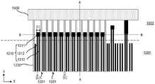
结合图1和图2,在一实施方式中,触控显示面板1000包括衬底1100以及引线层1200,引线层1200设置在衬底1100的第一侧,其中,衬底1100主要起支撑作用,引线层1200主要用于布线,同时引线层1200包括沿第一方向(图2中X方向)并列设置的多条触控连接走线1210和多条显示连接走线1220。衬底1100可以为柔性衬底,例如可以包括聚酰亚胺等材料。衬底1100可以为硬性衬底,例如可以是玻璃基板等。1 and 2 , in one embodiment, the
具体地,触控连接走线1210用于传输触控显示面板1000中的触控信号,显示连接走线1220用于传输触控显示面板1000中有画面显示相关显示信号。Specifically, the
其中,多条触控连接走线1210之间设置有沿第一方向X排列的多个间隔区域1201,至少两个间隔区域1201设置有显示连接走线1220,相邻间隔区域1201之间被触控连接走线1210所间隔。Among them, a plurality of
也就是说,多条显示连接走线1220分散在多个触控连接走线1210之间。例如,相邻两条触控连接走线1210之间存在一条显示连接走线1220,或者,相邻两条触控连接走线1210之间存在两条或者更多条显示连接走线1220。任一间隔区域1201可设置有一条或多条显示连接走线1220。That is to say, the plurality of
触控连接走线1210的至少部分区段可通过触控层制程工艺制作,受限于触控层制程的精度,导致触控连接走线1210的部分区段的PITCH(相邻两条触控连接走线1210的部分区段的中心距离)较大,例如大于40um,也就是说,相邻两条触控连接走线1210之间的空间较大。相邻触控连接走线1210之间的间距(可以是相邻第一导线段1211之间的间距)可等于触控层制程工艺所能达到的最小尺寸。触控连接走线1210的最大宽度(可以是第一导线段1211的线宽)可等于触控层制程工艺所能达到的最小尺寸。触控层制程工艺精度低,可以降低设备投入成本,降低掩模板(mask)的成本。而本实施方式就是利用相邻两条触控连接走线1210之间的空间放置显示连接走线1220,可以充分利用闲置的空间,缩小触控显示面板1000布线区域的宽度。其中,显示连接走线1220可通过制作显示层所采用的阵列(Array)制程工艺制作,故制作精度较高,可以制作线宽较小的显示连接走线1220,也可以将线间距制作的较小。At least some sections of the
继续参阅图2,触控连接走线1210包括连接的第一导线段1211和第二导线段1212。Continuing to refer to FIG. 2 , the
其中,第一导线段1211和第二导线段1212可以非同层设置,也可以同层设置。结合图3,当第一导线段1211和第二导线段1212非同层设置时,第一导线段1211与第二导线段1212可通过换线孔11电连接。Wherein, the
其中,显示连接走线1220和第二导线段1212可以同层设置,也可以非同层设置,例如在图4中,显示连接走线1220和第二导线段1212同层设置。The connection traces 1220 and the
在本实施方式中,可选的,多条触控连接走线1210的第一导线段1211沿第一方向X并列设置。可选的,多条触控连接走线1210的第二导线段1212沿第一方向X并列设置。受限于触控层制程的精度,,第一导线段1211的线宽D1大于显示连接走线1220的线宽D2。第一导线段1211可通过触控层制程工艺制作。第一导线段1211与触控层中的部分膜层可通过对同一导电层进行图案化得到,即通过同一构图工艺形成。相邻第一导线段1211之间的间距可等于触控层制程工艺所能达到的最小尺寸。如图2所示,相邻第一导线段1211之间的间距为在第一方向X上的间距。第一导线段1211的线宽可等于触控层制程工艺所能达到的最小尺寸。第一导线段1211的线宽D1为在垂直于第一导线段1211的延伸方向上的尺寸,示例性的,如图2所示,第一导线段1211的线宽D1为在第一方向X上的尺寸。显示连接走线1220的线宽D2为在垂直于显示连接走线1220的延伸方向上的尺寸,示例性的,如图2所示,第一导线段1211的线宽D1为在第一方向X上的尺寸。In this embodiment, optionally, the
可选的,第二导线段1212可以通过触控层制程工艺制作。第二导线段1212与触控层中的部分膜层可通过对同一导电层进行图案化得到,即通过同一构图工艺形成。相邻第二导线段1212之间的间距可等于触控层制程工艺所能达到的最小尺寸。第二导线段1212的线宽可等于触控层制程工艺所能达到的最小尺寸。第二导线段1212的线宽D3可以等于第一导线段1211的线宽D1。第二导线段1212的线宽D3为在垂直于第二导线段1212的延伸方向上的尺寸,示例性的,如图2所示,第二导线段1212的线宽为在第一方向X上的尺寸。Optionally, the
可选的,第二导线段1212可以通过制作显示层所采用的阵列制程工艺制作。第二导线段1212与显示层中的部分膜层可通过对同一导电层进行图案化得到,即通过同一构图工艺形成。第二导线段1212的线宽可以等于或小于第一导线段1211的线宽。Optionally, the
为了逐步缩小触控显示面板1000布线区域的宽度,可选的,第一导线段1211的线宽D1大于第二导线段1212的线宽D3,从而第二导线段1212所占布线区域的宽度可以小于第一导线段1211所占布线区域的宽度,进而可以减小引线层1200的体积,提高可弯折性能。In order to gradually reduce the width of the wiring area of the
结合图1和图5,在本实施方式中,触控显示面板1000包括可弯折区1001,以及位于可弯折区1001相对两侧的第一非弯折区1002以及邦定区1003。1 and 5 , in this embodiment, the
其中,第一非弯折区1002主要用于实现显示功能和触控功能,邦定区1003用于邦定显示驱动芯片、触控芯片和柔性电路板等邦定元件中的一种或多种,可弯折区1001可进行弯折,以使得邦定有邦定元件的邦定区1003位于第一非弯折区1002的背面,以实现触控显示面板1000的窄边框设计。示例性的,邦定区1003与柔性电路板邦定,显示驱动芯片和触控芯片可邦定于柔性电路板上。示例性的,显示驱动芯片和触控芯片邦定在邦定区1003上。Among them, the first
其中,多条触控连接走线1210和多条显示连接走线1220可由第一非弯折区1002延伸至可弯折区1001。具体地,设置触控连接走线1210和显示连接走线1220由第一非弯折区1002延伸至可弯折区1001,可以使得第一非弯折区1002中的显示信号和触控信号传输至可弯折区1001,从而在将可弯折区1001弯折后,第一非弯折区1002中的显示信号和触控信号能够传输至第一非弯折区1002的背面,即通过可弯折区1001,实现将触控显示面板1000正面的显示信号和触控信号传输至触控显示面板1000的背面。第一非弯折区1002指向可弯折区1001的方向可平行于方向Y。The plurality of
其中,第一导线段1211可位于第一非弯折区1002,第二导线段1212的至少部分可位于可弯折区1001。可选的,第二导线段1212的全部可位于可弯折区1001。第二导线段1212的一部分可位于可弯折区1001,另一部分可位于第一非弯折区1002。可选的,具体地,设置位于第一非弯折区1002的第一导线段1211的线宽D1大于位于可弯折区1001的第二导线段1212的线宽D3,可以使可弯折区1001的宽度小于第一非弯折区1002的宽度,降低将可弯折区1001进行弯折的难度。The
其中,邦定区1003还设置有邦定焊盘10031,邦定焊盘10031与触控连接走线1210和显示连接走线1220电连接。可以理解的是,与触控连接走线1210、显示连接走线1220电连接的邦定焊盘10031不是同一个。邦定焊盘10031可为多个。一部分邦定焊盘10031可与触控连接走线1210电连接;另一部分邦定焊盘10031可与显示连接走线1220电连接。The
具体地,在将驱动芯片和触控芯片等邦定元件邦定在邦定区1003上后,驱动芯片和触控芯片上的输入、输出引脚均与邦定焊盘10031电连接,其中,触控芯片通过邦定焊盘10031与触控连接走线1210电连接,驱动芯片通过邦定焊盘10031与显示连接走线1220电连接。Specifically, after bonding components such as the driver chip and the touch chip on the
结合图1和图5,触控显示面板1000还包括位于衬底1100的第一侧且沿远离衬底1100的方向依次层叠设置的显示层1300以及触控层1400。其中显示层1300用于显示画面,触控层1400用于感应用户的触摸信号,且显示层1300以及触控层1400位于第一非弯折区1002。Referring to FIG. 1 and FIG. 5 , the
其中,显示层1300可包括位于衬底1100的第一侧且沿远离衬底1100的方向依次层叠设置的驱动阵列层和发光器件层。驱动阵列层可包括层叠设置的半导体层、导电层和绝缘层等。驱动阵列层可用于形成薄膜晶体管、储存电容、扫描线以及数据线等结构,触控层1400通常触控电极等结构。触控层1400可为电容式触控层等。电容式触控层可包括自容式触控层或互容式触控层。Wherein, the
发光器件层可为有机发光器件层等。发光器件层可包括沿触控显示面板的厚度方向层叠设置的阳极层、发光功能层和阴极层。The light emitting device layer may be an organic light emitting device layer or the like. The light-emitting device layer may include an anode layer, a light-emitting functional layer, and a cathode layer that are stacked along the thickness direction of the touch display panel.
可选的,触控显示面板1000还包括薄膜封装层。薄膜封装层可位于发光器件层和触控层1400之间。薄膜封装层可包括沿触控显示面板的厚度方向交替层叠设置的有机层和无机层。Optionally, the
其中,第一非弯折区1002包括显示区10021以及位于显示区10021外围的边框区10022(为非显示区),可弯折区1001与边框区10022连接,其中,显示层1300以及触控层1400具体位于显示区10021,引线层1200位于边框区10022、可弯折区1001以及邦定区1003,也就是说,触控连接走线1210中的第一导线段1211可位于边框区10022中。The first
其中参阅图1,在本实施方式中,为了减小将可弯折区1001进行弯折的难度,将位于可弯折区1001的引线层1200的厚度设置成小于位于第一非弯折区1002的引线层1200的厚度。1 , in this embodiment, in order to reduce the difficulty of bending the
其中,显示连接走线1220与显示层1300电连接,触控连接走线1210与触控层1400电连接。The
其中,显示连接走线1220可以与显示层1300中的扫描线或者数据线、电源线等结构同层设置,即对同一导电层进行图案化而得到显示连接走线1220以及扫描线,或者得到显示连接走线1220以及数据线。Wherein, the
其中,第一导线段1211可以与触控层1400中的触控电极同层设置,即对同一导电层进行图案化而得到第一导线段1211以及触控电极。The
其中,为了屏蔽相邻两条触控连接走线1210所传输信号之间的干扰,设置显示连接走线1220均为与显示层1300电连接的直流电位线,也就是说,多条显示连接走线1220均传输的是直流信号。Among them, in order to shield the interference between the signals transmitted by the adjacent two touch connection traces 1210, the display connection traces 1220 are set to be DC potential lines electrically connected to the
具体地,设置多条显示连接走线1220传输直流信号,既可以屏蔽相邻两条触控连接走线1210所传输信号之间的干扰,也可以避免显示连接走线1220所传输的信号干扰触控连接走线1210所传输的信号。Specifically, setting a plurality of
在本实施方式中,多条显示连接走线1220均为与发光器件层中的阴极层电连接的直流电位线。具体地,发光器件层通常包括阳极层以及阴极层,而多条显示连接走线1220均与阴极层电连接,也就是说,多条显示连接走线1220均为ELVSS信号线,相当于低电位信号线。In this embodiment, the plurality of
其中,发光器件层具体可以是有机发光二极管(OLED)层,也可以是微发光二极管(Micro-LED)层,在此不做限制。The light-emitting device layer may specifically be an organic light-emitting diode (OLED) layer or a micro-light-emitting diode (Micro-LED) layer, which is not limited herein.
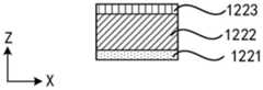
在本实施方式中,多条第二导线段1212与多条显示连接走线1220同层设置。多条第二导线段1212与多条显示连接走线1220可材料相同,也就是说,对同一层导电层进行图案化,得到多条第二导线段1212以及多条显示连接走线1220。In this embodiment, the plurality of
其中,将第二导线段1212与显示连接走线1220同层设置,可以减小可弯折区1001的走线层的层数,减小可弯折区1001的厚度,可以减小在将可弯折区1001进行弯折时,各个材料层之间的应力,从而提高可弯折区1001的弯折性能,避免在弯折过程中,可弯折区1001发生断裂。Wherein, arranging the
需要说明的是,在其他实施方式中,多条第二导线段1212以及多条显示连接走线1220也可以非同层设置。It should be noted that, in other embodiments, the plurality of
在本实施方式中,参阅图6,第二导线段1212以及显示连接走线1220均为叠层结构,且叠层结构包括依次设置的第一导电材料层1221、第二导电材料层1222以及第三导电材料层1223;其中,第一导电材料层1221以及第三导电材料层1223的厚度小于第二导电材料层1222的厚度,第一导电材料层1221以及第三导电材料层1223的耐腐蚀性强于第二导电材料层1222的耐腐蚀性。第一导电材料层1221、第二导电材料层1222以及第三导电材料层1223可沿衬底1100的厚度方向Z依次层叠设置。第一导电材料层1221、第二导电材料层1222以及第三导电材料层1223可包括金属材料等。In this embodiment, referring to FIG. 6 , the
具体地,第二导电材料层1222作为传输信号的主体部,第一导电材料层1221以及第三导电材料层1223的厚度小于第二导电材料层1222的厚度,用于保护第二导电材料层1222,避免随着时间的推移,第二导电材料层1222被外界水汽腐蚀,从而提高第二导线段1212以及显示连接走线1220的可靠性,进而提供可弯折区1001的可靠性。Specifically, the second
在一应用场景中,考虑到钛具有较强的耐腐蚀性能和弯折性能,铝具有较强的导电性能和弯折性能,设置第一导电材料层1221以及第三导电材料层1223的材料均为钛,第二导电材料层1222的材料为铝。In an application scenario, considering that titanium has strong corrosion resistance and bending performance, and aluminum has strong electrical conductivity and bending performance, the materials for setting the first
其中,本申请对第一导电材料层1221、第二导电材料层1222以及第三导电材料层1223的材料不做限制,例如在其他实施方式中,第二导电材料层1222的材料也可以是铜。The present application does not limit the materials of the first
需要说明的是,在其他实施方式中,第二导线段1212和显示连接走线140也可以是单层结构,例如触控连接走线130和显示连接走线140的材料为铝。It should be noted that, in other embodiments, the
继续参阅图2,在本实施方式中,每条触控连接走线1210中的第二导线段1212为至少两条且沿第一方向X并列排布,每条触控连接走线1210中的第一导线段1211与至少两条第二导线段1212电连接。Continuing to refer to FIG. 2 , in this embodiment, at least two
具体地,相比较于触控连接走线1210只包括一条第一导线段1211和一条第二导线段1212,设置至少两条第二导线段1212与第一导线段1211电连接,可以减小触控连接走线1210的传输阻抗。Specifically, compared with the
需要说明的是,在其他实施方式中,触控连接走线1210也可以只包括一条第一导线段1211和一条第二导线段1212,此时可以通过增大线宽的方式减小触控连接走线1210的传输阻抗。It should be noted that, in other embodiments, the
参阅图2,在本实施方式中,触控连接走线1210和显示连接走线1220的延伸方向均与第一方向X相交,例如可以是垂直,但是在其他实施方式中,触控连接走线1210和显示连接走线1220的延伸方向也可以不与第一方向垂直,例如在图7实施方式中,第二导线段1212和显示连接走线1220为折线形,而非图2中的直线形,使得可弯折区1001中的第二导线段1212和显示连接走线1220整体占据区域在第一方向X上的宽度小于第一非弯折区1002的第一导线段1211和显示连接走线1220整体占据区域在第一方向X上的宽度,进一步降低布线区域的宽度。Referring to FIG. 2 , in this embodiment, the extending directions of the touch connection traces 1210 and the display connection traces 1220 both intersect the first direction X, for example, may be vertical, but in other embodiments, the touch connection traces The extension direction of 1210 and the
继续参阅图5,在本实施方式中,显示区10021可为矩形或不同于矩形的异形显示区,显示区10021可呈圆形、椭圆形、或边数大于或者等于6的正多边形或圆角正多边形等。也就是说本实施方式的触控显示面板1000适用于屏幕为圆形、椭圆形、或边数大于或者等于6的正多边形的电子设备,例如,触控显示面板1000应用于手表。Continuing to refer to FIG. 5 , in this embodiment, the
需要说明的是,在其他实施方式中,显示区10021也可以是矩形,本申请对显示区10021的形状不做限制。It should be noted that, in other embodiments, the
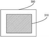
参阅图9,图9是本申请电子设备一实施方式的结构示意图,该电子设备300包括触控显示面板310。Referring to FIG. 9 , FIG. 9 is a schematic structural diagram of an embodiment of an electronic device of the present application. The
其中触控显示面板310与上述任一项实施方式中的触控显示面板结构相同,具体可参见上述实施方式,在此不再赘述。The structure of the
在一应用场景中,电子设备300可以是显示区域呈圆形、椭圆形、或边数大于或者等于6的正多边形的设备。In an application scenario, the
结合图1、图2以及图10,在一实施方式中,触控显示面板的制作方法包括:1 , FIG. 2 and FIG. 10 , in one embodiment, the manufacturing method of the touch display panel includes:
S410:提供衬底1100。S410: Provide the
S420:在衬底1100上形成引线层1200,引线层1200包括沿第一方向并列设置的多条触控连接走线1210和多条显示连接走线1220;多条触控连接走线1210之间设置有沿第一方向排列的多个间隔区域1201,至少两个间隔区域1201设置有显示连接走线1220,相邻间隔区域1201之间被触控连接走线1210所间隔,触控连接走线1210的至少部分的制作工艺精度小于显示连接走线1220的制作工艺精度。S420 : forming a
其中,触控连接走线1210的部分或全部的制作工艺精度小于显示连接走线1220的制作工艺精度。触控连接走线1210的部分或全部通过制作触控层所用的制作工艺制作,显示连接走线1220通过制作显示层所采用的阵列制程工艺制作。触控层制程工艺精度低,可以降低设备投入成本,降低掩模板(mask)的成本。Wherein, the manufacturing process precision of part or all of the touch connection traces 1210 is smaller than that of the display connection traces 1220 . Part or all of the
可选的,触控连接走线1210包括连接的第一导线段1211和第二导线段1212,第一导线段1211的制作工艺精度小于显示连接走线1220的制作工艺精度,第二导线段1212的制作工艺精度与显示连接走线1220的制作工艺精度相同。Optionally, the
具体地,第一导线段1211的制作工艺精度小于显示连接走线1220的制作工艺精度。第一导线段1211的制作工艺所制作的最小线宽尺寸小于显示连接走线1220的制作工艺所制作的最小线宽尺寸。第一导线段1211的制作工艺所制作的最小线间距尺寸小于显示连接走线1220的制作工艺所制作的最小线间距尺寸。第一导线段1211的线宽可等于第一导线段1211的制作工艺所制作的最小线宽尺寸。相邻第一导线段1211之间的线间距可等于第一导线段1211的制作工艺所制作的最小线间距尺寸。第一导线段1211的线宽D1大于显示连接走线1220的线宽D2。Specifically, the manufacturing process precision of the
第二导线段1212的制作工艺精度与显示连接走线1220的制作工艺精度相同。可选的,第二导线段1212的线宽D3与显示连接走线1220的线宽D相等。The manufacturing process precision of the
在现有技术中,由于第一导线段1211的制作工艺精度低,导致相邻第一导线段1211之间的间距大,存在闲置空间,而本实施方式在制作时,将显示连接走线1220放置在相邻两条触控连接走线1210之间的闲置空间中,可以缩小触控显示面板布线区域的宽度。In the prior art, due to the low manufacturing process precision of the
其中,采用本实施方式中的制作方法所制作的触控显示面板与上述任一项实施方式中的触控显示面板结构相同,具体可参见上述实施方式,在此不再赘述。Wherein, the touch display panel manufactured by the manufacturing method in this embodiment has the same structure as the touch display panel in any of the above-mentioned embodiments. For details, refer to the above-mentioned embodiments, which will not be repeated here.
在相关技术中,如图11所示,多条显示连接走线240位于触控连接走线的两侧,触控连接走线之间设置虚拟走线20。In the related art, as shown in FIG. 11 , a plurality of
同时受限于触控层制程的精度,非弯折区2023的触控连接走线的第一导线段220的PITCH(相邻两条第一导线段220的中心距离)大于40um,而弯折区201的走线的PITCH只有10um左右,因此在弯折区201,触控连接走线的第一导线段220与相邻两条第二导线段230电连接,第二导线段230之间存在闲置的虚拟走线20(dummy走线),造成空间的浪费。闲置的弯折走线20不用于传输信号或电位。At the same time, limited by the precision of the touch layer process, the PITCH (the distance between the centers of two adjacent first wire segments 220 ) of the
图2的技术方案与图11的技术方案相比,图2的技术方案可以利用显示连接走线1220替换闲置的虚拟走线20(dummy走线),能够缩小可弯折区的宽度。Compared with the technical solution in FIG. 11 , the technical solution in FIG. 2 can replace the idle dummy wiring 20 (dummy wiring) with the
以上所述仅为本申请的实施方式,并非因此限制本申请的专利范围,凡是利用本申请说明书及附图内容所作的等效结构或等效流程变换,或直接或间接运用在其他相关的技术领域,均同理包括在本申请的专利保护范围内。The above description is only an embodiment of the present application, and is not intended to limit the scope of the patent of the present application. Any equivalent structure or equivalent process transformation made by using the contents of the description and drawings of the present application, or directly or indirectly applied to other related technologies Fields are similarly included within the scope of patent protection of this application.
Claims (10)
Priority Applications (1)
| Application Number | Priority Date | Filing Date | Title |
|---|---|---|---|
| CN202210399261.XACN114967988A (en) | 2022-04-15 | 2022-04-15 | Touch display panel and manufacturing method thereof |
Applications Claiming Priority (1)
| Application Number | Priority Date | Filing Date | Title |
|---|---|---|---|
| CN202210399261.XACN114967988A (en) | 2022-04-15 | 2022-04-15 | Touch display panel and manufacturing method thereof |
Publications (1)
| Publication Number | Publication Date |
|---|---|
| CN114967988Atrue CN114967988A (en) | 2022-08-30 |
Family
ID=82977234
Family Applications (1)
| Application Number | Title | Priority Date | Filing Date |
|---|---|---|---|
| CN202210399261.XAPendingCN114967988A (en) | 2022-04-15 | 2022-04-15 | Touch display panel and manufacturing method thereof |
Country Status (1)
| Country | Link |
|---|---|
| CN (1) | CN114967988A (en) |
Citations (4)
| Publication number | Priority date | Publication date | Assignee | Title |
|---|---|---|---|---|
| CN104142748A (en)* | 2013-05-09 | 2014-11-12 | 宸正光电(厦门)有限公司 | Touch panel |
| CN206193731U (en)* | 2016-10-26 | 2017-05-24 | 上海天马微电子有限公司 | Touch display panel and display device |
| CN213545245U (en)* | 2020-12-22 | 2021-06-25 | 信利(仁寿)高端显示科技有限公司 | Touch display device |
| CN114185454A (en)* | 2021-12-13 | 2022-03-15 | 武汉华星光电半导体显示技术有限公司 | Display panel and electronic device |
- 2022
- 2022-04-15CNCN202210399261.XApatent/CN114967988A/enactivePending
Patent Citations (4)
| Publication number | Priority date | Publication date | Assignee | Title |
|---|---|---|---|---|
| CN104142748A (en)* | 2013-05-09 | 2014-11-12 | 宸正光电(厦门)有限公司 | Touch panel |
| CN206193731U (en)* | 2016-10-26 | 2017-05-24 | 上海天马微电子有限公司 | Touch display panel and display device |
| CN213545245U (en)* | 2020-12-22 | 2021-06-25 | 信利(仁寿)高端显示科技有限公司 | Touch display device |
| CN114185454A (en)* | 2021-12-13 | 2022-03-15 | 武汉华星光电半导体显示技术有限公司 | Display panel and electronic device |
Similar Documents
| Publication | Publication Date | Title |
|---|---|---|
| CN108417604B (en) | Display panel and display device | |
| CN207557624U (en) | A kind of array substrate, display panel and display device | |
| EP3300466A1 (en) | Narrow border displays for electronic devices | |
| CN108389869A (en) | Flexible display panel | |
| WO2022241890A1 (en) | Display panel and display apparatus | |
| JP7634990B2 (en) | Flexible circuit board and manufacturing method thereof, electronic device module and electronic device | |
| CN109828691B (en) | Touch screen for narrow-frame electronic equipment and electronic equipment | |
| WO2020087837A1 (en) | Touch control display panel and display device | |
| TW201512914A (en) | Touch control panel and touch display device | |
| CN205318347U (en) | Touch control display panel | |
| WO2020156595A9 (en) | Flexible circuit board and manufacturing method, display device, circuit board structure and display panel thereof | |
| US20210212207A1 (en) | Flexible printed circuit and manufacture method thereof, electronic device module and electronic device | |
| CN111142714A (en) | Display panel and display device | |
| TW201504892A (en) | Touch electrode structure and touch panel thereof | |
| US11086460B2 (en) | Touch substrate, method for manufacturing same, and touch device | |
| CN110515505A (en) | A touch substrate and its manufacturing method, touch panel | |
| TWI575434B (en) | Touch panels | |
| CN112183396B (en) | Display components and display devices | |
| CN113539058B (en) | Display module and terminal | |
| TW202213051A (en) | Touch display module and touch display device | |
| CN105954952A (en) | Display device, display panel and manufacturing method for display panel | |
| CN114967988A (en) | Touch display panel and manufacturing method thereof | |
| CN114924664B (en) | Touch substrate and display panel | |
| CN114356154B (en) | Touch control substrate and display device | |
| TWI463373B (en) | Touch panel and manufacturing method thereof |
Legal Events
| Date | Code | Title | Description |
|---|---|---|---|
| PB01 | Publication | ||
| PB01 | Publication | ||
| SE01 | Entry into force of request for substantive examination | ||
| SE01 | Entry into force of request for substantive examination |