CN114925013A - CPLD-based I2C signal transparent transmission method, device and medium - Google Patents
CPLD-based I2C signal transparent transmission method, device and mediumDownload PDFInfo
- Publication number
- CN114925013A CN114925013ACN202210404241.7ACN202210404241ACN114925013ACN 114925013 ACN114925013 ACN 114925013ACN 202210404241 ACN202210404241 ACN 202210404241ACN 114925013 ACN114925013 ACN 114925013A
- Authority
- CN
- China
- Prior art keywords
- signal
- state
- transmitted
- buffer
- tri
- Prior art date
- Legal status (The legal status is an assumption and is not a legal conclusion. Google has not performed a legal analysis and makes no representation as to the accuracy of the status listed.)
- Granted
Links
Images


Classifications
- G—PHYSICS
- G06—COMPUTING OR CALCULATING; COUNTING
- G06F—ELECTRIC DIGITAL DATA PROCESSING
- G06F13/00—Interconnection of, or transfer of information or other signals between, memories, input/output devices or central processing units
- G06F13/38—Information transfer, e.g. on bus
- G06F13/42—Bus transfer protocol, e.g. handshake; Synchronisation
- G06F13/4282—Bus transfer protocol, e.g. handshake; Synchronisation on a serial bus, e.g. I2C bus, SPI bus
- G—PHYSICS
- G06—COMPUTING OR CALCULATING; COUNTING
- G06F—ELECTRIC DIGITAL DATA PROCESSING
- G06F2213/00—Indexing scheme relating to interconnection of, or transfer of information or other signals between, memories, input/output devices or central processing units
- G06F2213/0016—Inter-integrated circuit (I2C)
Landscapes
- Engineering & Computer Science (AREA)
- Theoretical Computer Science (AREA)
- Physics & Mathematics (AREA)
- General Engineering & Computer Science (AREA)
- General Physics & Mathematics (AREA)
- Information Transfer Systems (AREA)
- Programmable Controllers (AREA)
Abstract
Translated fromChinese
Description
Translated fromChinese技术领域technical field
本说明书涉及交换机硬件技术领域,尤其涉及一种基于CPLD的I2C信号透传方法、设备及介质。This specification relates to the technical field of switch hardware, and in particular, to a method, device and medium for transparent transmission of I2C signals based on CPLD.
背景技术Background technique
交换机使用支持数字诊断监控(Digital Diagnostic Monitoring,DDM)的光模块时,需要通过I2C(Inter-Integrated Circuit)总线对多个光模块进行读取操作,因为多个光模块I2C设备地址相同,所以需要多路I2C总线,分别与单个光模块通信,实际通常使用复杂可编程逻辑器件(Complex Programmable Logic Device,CPLD)进行I2C总线的扩展,将一路I2C总线扩展为多路I2C总线,选中通道后进行I2C信号的双向透传。When the switch uses an optical module that supports Digital Diagnostic Monitoring (DDM), it needs to read multiple optical modules through the I2C (Inter-Integrated Circuit) bus. Because the I2C device addresses of multiple optical modules are the same, it is necessary to Multiple I2C buses communicate with a single optical module respectively. In practice, Complex Programmable Logic Device (CPLD) is usually used to expand the I2C bus, and one I2C bus is expanded into multiple I2C buses. After selecting the channel, I2C is performed. Bidirectional transparent transmission of signals.
当前常用的I2C信号透传方法是通过CPLD分别实现一个I2C从机和一个I2C主机,I2C主机主动读取光模块DDM信息,并将读取的DDM信息存储至CPLD,由I2C从机读取DDM信息后,上报DDM信息。现有技术中的信号透传方法占用了较多的CPLD硬件资源,并且无法保证传输的实时性。The currently commonly used I2C signal transparent transmission method is to realize an I2C slave and an I2C master respectively through CPLD. The I2C master actively reads the DDM information of the optical module, and stores the read DDM information in the CPLD, and the I2C slave reads the DDM. After the information is received, report the DDM information. The signal transparent transmission method in the prior art occupies more CPLD hardware resources, and cannot guarantee the real-time transmission.
发明内容SUMMARY OF THE INVENTION
本说明书一个或多个实施例提供了一种基于CPLD的I2C信号透传方法、设备及介质,用于解决如下技术问题:现有技术中的信号透传方法占用了较多的CPLD硬件资源,并且无法保证传输的实时性。One or more embodiments of this specification provide a CPLD-based I2C signal transparent transmission method, device and medium, which are used to solve the following technical problems: the signal transparent transmission method in the prior art occupies a lot of CPLD hardware resources, And the real-time transmission cannot be guaranteed.
本说明书一个或多个实施例采用下述技术方案:One or more embodiments of this specification adopt the following technical solutions:
本说明书一个或多个实施例提供一种基于CPLD的I2C信号透传方法,应用于I2C信号透传系统,其中,所述I2C信号透传系统包括设置在所述CPLD芯片中的方向判断模块和方向控制模块、I2C主设备以及I2C从设备,所述方法包括:基于I2C信号透传系统的复位信号的触发,通过所述方向判断模块根据所述复位信号,生成待传输I2C信号的方向信号;其中,所述待传输I2C信号的方向信号用于表示所述待传输I2C信号的传输方向,包括第一方向和第二方向,所述第一方向为所述I2C主设备输出且所述I2C从设备输入的信号传输方向,所述第二方向为所述I2C从设备输出且所述I2C主设备输入的信号传输方向;通过所述方向控制模块,根据所述待传输I2C信号的方向信号,控制所述待传输I2C信号按照所述方向信号进行透传。One or more embodiments of this specification provide a CPLD-based I2C signal transparent transmission method, which is applied to an I2C signal transparent transmission system, wherein the I2C signal transparent transmission system includes a direction judgment module arranged in the CPLD chip and a A direction control module, an I2C master device, and an I2C slave device, the method comprising: triggering a reset signal based on an I2C signal transparent transmission system, and generating a direction signal of the I2C signal to be transmitted by the direction judgment module according to the reset signal; The direction signal of the I2C signal to be transmitted is used to indicate the transmission direction of the I2C signal to be transmitted, including a first direction and a second direction, the first direction is the output of the I2C master device and the I2C slave The signal transmission direction input by the device, the second direction is the signal transmission direction output by the I2C slave device and input by the I2C master device; through the direction control module, according to the direction signal of the I2C signal to be transmitted, control The I2C signal to be transmitted is transparently transmitted according to the direction signal.
进一步地,所述方向控制模块包括:第一反相器、第一三态缓冲器、第二三态缓冲器、第一缓冲器以及第二缓冲器;其中,所述第一反相器的输入端用于输入所述方向信号,所述第一反相器的输出端与所述第一三态缓冲器的选项卡通输入端相连;所述第一三态缓冲器的输入端用于接收所述第二缓冲器的输出端的信号,所述第一三态缓冲器的输出端与所述I2C主设备相连;所述第一缓冲器的输入端用于输入所述I2C主设备的待传输I2C信号,所述第一缓冲器的输出端与所述第二三态缓冲器的输入端相连;所述第二三态缓冲器的选项卡通输入端用于输入所述方向信号,所述第二三态的输出端与所述I2C从设备相连;所述第二缓冲器的输入端用于输入所述I2C从设备的待传输I2C信号;通过所述方向控制模块,根据所述待传输I2C信号的方向信号,控制所述待传输I2C信号按照所述方向信号进行透传,具体包括:将所述待传输I2C信号的方向信号输入至所述第一反相器的输入端和所述第二三态缓冲器的选项卡通输入端;根据所述待传输I2C信号的方向信号,确定出所述第一三态缓冲器和所述第二三态缓冲器的工作状态;根据所述第一三态缓冲器和所述第二三态缓冲器的工作状态,生成所述I2C主设备与所述I2C从设备之间的透传路线。Further, the direction control module includes: a first inverter, a first tri-state buffer, a second tri-state buffer, a first buffer and a second buffer; wherein, the first inverter The input terminal is used for inputting the direction signal, and the output terminal of the first inverter is connected with the option card input terminal of the first three-state buffer; the input terminal of the first three-state buffer is used for receiving The signal of the output terminal of the second buffer, the output terminal of the first three-state buffer is connected to the I2C master device; the input terminal of the first buffer is used to input the pending transmission of the I2C master device I2C signal, the output end of the first buffer is connected to the input end of the second tri-state buffer; the option card input end of the second tri-state buffer is used to input the direction signal, the third The output terminal of two or three states is connected to the I2C slave device; the input terminal of the second buffer is used to input the I2C signal to be transmitted from the I2C slave device; through the direction control module, according to the I2C to be transmitted I2C signal The direction signal of the signal, and controlling the I2C signal to be transmitted to be transparently transmitted according to the direction signal, which specifically includes: inputting the direction signal of the I2C signal to be transmitted to the input end of the first inverter and the first inverter. The option card input terminal of the two-three-state buffer; according to the direction signal of the I2C signal to be transmitted, the working state of the first three-state buffer and the second three-state buffer is determined; according to the first three-state buffer The working states of the tri-state buffer and the second tri-state buffer generate a transparent transmission route between the I2C master device and the I2C slave device.
进一步地,根据所述待传输I2C信号的方向信号,确定出所述第一三态缓冲器和所述第二三态缓冲器的工作状态,具体包括:当所述待传输I2C信号的方向信号为所述第一方向时,所述第一三态缓冲器为禁能状态,其中,在所述禁能状态下所述第一三态缓冲器的输出端为高阻态;当所述待传输I2C信号的方向信号为所述第二方向时,所述第二三态缓冲器为禁能状态,其中,在所述禁能状态下所述第二三态缓冲器的输出端为高阻态。Further, determining the working states of the first tri-state buffer and the second tri-state buffer according to the direction signal of the I2C signal to be transmitted, specifically including: when the direction signal of the I2C signal to be transmitted is When the direction is the first direction, the first tri-state buffer is in a disabled state, wherein in the disabled state, the output end of the first tri-state buffer is in a high-impedance state; When the direction signal for transmitting the I2C signal is the second direction, the second tri-state buffer is in a disabled state, wherein in the disabled state, the output end of the second tri-state buffer is a high impedance state.
进一步地,根据所述第一三态缓冲器和所述第二三态缓冲器的工作状态,生成所述I2C主设备与所述I2C从设备之间的透传路线,具体包括:当所述第一三态缓冲器为禁能状态时,所述I2C主设备与所述I2C从设备之间的透传路线为:所述I2C主设备的所述待传输I2C信号输入至所述第一缓冲器的输入端,通过所述第一缓冲器的输出端输出所述待传输I2C信号,并将所述待传输I2C信号输入至所述第二三态缓冲器的输入端,通过所述第二三态缓冲器的输出端输出至所述I2C从设备;当所述第二三态缓冲器为禁能状态时,所述I2C从设备与所述I2C主设备之间的透传路线为:所述I2C从设备的所述待传输I2C信号输入至所述第二缓冲器的输入端,通过所述第二缓冲器的输出端输出所述待传输I2C信号,并将所述待传输I2C信号输入至所述第一三态缓冲器的输入端,通过所述第一三态缓冲器的输出端输出至所述I2C主设备。Further, generating a transparent transmission route between the I2C master device and the I2C slave device according to the working states of the first tri-state buffer and the second tri-state buffer, specifically including: when the When the first tri-state buffer is in a disabled state, the transparent transmission route between the I2C master device and the I2C slave device is: the I2C signal to be transmitted of the I2C master device is input to the first buffer The input terminal of the 3-state buffer, the output terminal of the first buffer outputs the I2C signal to be transmitted, and the I2C signal to be transmitted is input to the input terminal of the second three-state buffer, and the I2C signal to be transmitted is input to the input terminal of the second three-state buffer through the second The output end of the tri-state buffer is output to the I2C slave device; when the second tri-state buffer is disabled, the transparent transmission route between the I2C slave device and the I2C master device is: The I2C signal to be transmitted of the I2C slave device is input to the input end of the second buffer, the output end of the second buffer outputs the I2C signal to be transmitted, and the I2C signal to be transmitted is input to the input terminal of the first tri-state buffer, and output to the I2C master device through the output terminal of the first tri-state buffer.
进一步地,通过所述方向判断模块根据所述复位信号,生成I2C信号的方向信号,具体包括:根据所述复位信号,通过所述方向判断模块确定所述I2C信号透传系统的状态机状态,所述I2C信号透传系统的状态机状态包括空闲状态、设备地址传输状态、读写标志位判断状态、从设备应答状态、第一方向数据传输状态、第二方向数据传输状态以及主设备应答状态;根据所述I2C信号透传系统的状态机状态,确定所述待传输I2C信号的方向信号。Further, generating the direction signal of the I2C signal by the direction judging module according to the reset signal, specifically comprising: determining the state machine state of the I2C signal transparent transmission system by the direction judging module according to the reset signal, The state machine state of the I2C signal transparent transmission system includes idle state, device address transmission state, read and write flag bit judgment state, slave device response state, first direction data transmission state, second direction data transmission state and master device response state. ; Determine the direction signal of the I2C signal to be transmitted according to the state machine state of the I2C signal transparent transmission system.
进一步地,所述空闲状态用于表示所述I2C信号透传系统中无信号传输的状态;所述设备地址传输状态用于表示所述I2C主设备向所述I2C从设备依次发送指定位数的设备地址的状态;所述读写标志位判断状态用于表示所述I2C主设备向所述I2C从设备发送读写标志位的状态;从设备应答状态用于表示所述I2C从设备向所述I2C主设备发送应答位或否应答位的状态;所述第一方向数据传输状态用于表示所述I2C主设备向所述I2C从设备依次发送指定数据的状态,其中,所述指定数据包括所述I2C从设备的寄存器地址或待传输至所述I2C从设备的寄存器中的数据;所述第二方向数据传输状态用于表示所述I2C从设备向所述I2C主设备依次发送预设数据的状态,其中,所述预设数据为待传输至所述I2C主设备的寄存器中的数据;所述主设备应答状态用于表示所述I2C主设备向所述I2从设备发送应答位或否应答位的状态。Further, the idle state is used to indicate the state of no signal transmission in the I2C signal transparent transmission system; the device address transmission state is used to indicate that the I2C master device sequentially sends the specified number of bits to the I2C slave device. The state of the device address; the read-write flag bit judgment state is used to indicate the state of the I2C master device sending the read-write flag bit to the I2C slave device; the slave device response state is used to indicate that the I2C slave device sends to the I2C slave device. The state in which the I2C master device sends an acknowledgement bit or no acknowledgement bit; the first-direction data transmission state is used to indicate the state in which the I2C master device sends designated data to the I2C slave device in sequence, wherein the designated data includes all The register address of the I2C slave device or the data to be transmitted to the register of the I2C slave device; the second direction data transmission state is used to indicate that the I2C slave device sends preset data to the I2C master device in turn. state, wherein the preset data is the data to be transmitted to the register of the I2C master device; the master device response state is used to indicate that the I2C master device sends a response bit or no response to the I2 slave device bit status.
进一步地,根据所述I2C信号透传系统的状态机状态,确定所述待传输I2C信号的方向信号,具体包括:当所述I2C信号透传系统的状态机状态为所述空闲状态、所述设备地址传输状态、所述第一方向数据传输状态以及所述主设备应答状态中的任意一种状态时,将所述待传输I2C信号的方向信号确定为所述第一方向。Further, determining the direction signal of the I2C signal to be transmitted according to the state machine state of the I2C signal transparent transmission system, specifically including: when the state machine state of the I2C signal transparent transmission system is the idle state, the In any state of the device address transmission state, the first direction data transmission state, and the master device response state, the direction signal of the to-be-transmitted I2C signal is determined as the first direction.
进一步地,根据所述I2C信号透传系统的状态机状态,确定所述I2C信号的方向信号,具体包括:当所述I2C信号透传系统的状态机状态为所述读写标志位判断状态、所述从设备应答状态以及所述第二方向数据传输状态中的任意一种状态时,将所述待传输I2C信号的方向信号确定为所述第二方向。Further, determining the direction signal of the I2C signal according to the state machine state of the I2C signal transparent transmission system, specifically including: when the state machine state of the I2C signal transparent transmission system is the read-write flag bit judgment state, When the slave device is in any one of the response state and the data transmission state in the second direction, the direction signal of the I2C signal to be transmitted is determined as the second direction.
本说明书一个或多个实施例提供一种基于CPLD的I2C信号透传设备,包括:One or more embodiments of this specification provide a CPLD-based I2C signal transparent transmission device, including:
至少一个处理器;以及,at least one processor; and,
与所述至少一个处理器通信连接的存储器;其中,a memory communicatively coupled to the at least one processor; wherein,
所述存储器存储有可被所述至少一个处理器执行的指令,所述指令被所述至少一个处理器执行,以使所述至少一个处理器能够:基于I2C信号透传系统的复位信号的触发,通过方向判断模块根据所述复位信号,生成待传输I2C信号的方向信号;其中,所述待传输I2C信号的方向信号用于表示所述待传输I2C信号的传输方向,包括第一方向和第二方向,所述第一方向为所述I2C主设备输出且所述I2C从设备输入的信号传输方向,所述第二方向为所述I2C从设备输出且所述I2C主设备输入的信号传输方向;通过方向控制模块,根据所述待传输I2C信号的方向信号,控制所述待传输I2C信号按照所述方向信号进行透传。The memory stores instructions executable by the at least one processor, the instructions are executed by the at least one processor, so that the at least one processor can: based on the triggering of the reset signal of the I2C signal transparent transmission system , the direction judging module generates the direction signal of the I2C signal to be transmitted according to the reset signal; wherein, the direction signal of the I2C signal to be transmitted is used to indicate the transmission direction of the I2C signal to be transmitted, including the first direction and the first direction. Two directions, the first direction is the signal transmission direction output by the I2C master device and input by the I2C slave device, and the second direction is the signal transmission direction output by the I2C slave device and input by the I2C master device. ; Through the direction control module, according to the direction signal of the I2C signal to be transmitted, the I2C signal to be transmitted is controlled to be transparently transmitted according to the direction signal.
本说明书一个或多个实施例提供的一种非易失性计算机存储介质,存储有计算机可执行指令,所述计算机可执行指令设置为:基于I2C信号透传系统的复位信号的触发,通过方向判断模块根据所述复位信号,生成待传输I2C信号的方向信号;其中,所述待传输I2C信号的方向信号用于表示所述待传输I2C信号的传输方向,包括第一方向和第二方向,所述第一方向为所述I2C主设备输出且所述I2C从设备输入的信号传输方向,所述第二方向为所述I2C从设备输出且所述I2C主设备输入的信号传输方向;通过方向控制模块,根据所述待传输I2C信号的方向信号,控制所述待传输I2C信号按照所述方向信号进行透传。A non-volatile computer storage medium provided by one or more embodiments of this specification stores computer-executable instructions, and the computer-executable instructions are set to: based on the trigger of the reset signal of the I2C signal transparent transmission system, through the direction The judgment module generates the direction signal of the I2C signal to be transmitted according to the reset signal; wherein, the direction signal of the I2C signal to be transmitted is used to indicate the transmission direction of the I2C signal to be transmitted, including the first direction and the second direction, The first direction is the signal transmission direction output by the I2C master device and input by the I2C slave device, and the second direction is the signal transmission direction output by the I2C slave device and input by the I2C master device; through direction The control module, according to the direction signal of the I2C signal to be transmitted, controls the I2C signal to be transmitted to be transparently transmitted according to the direction signal.
本说明书实施例采用的上述至少一个技术方案能够达到以下有益效果:通过上述技术方案,CPLD仅用于传输,无需将数据进行存储后再读取,节省了CPLD的硬件资源,并且保证了信号传输的实时性。The above-mentioned at least one technical solution adopted in the embodiments of this specification can achieve the following beneficial effects: through the above-mentioned technical solution, the CPLD is only used for transmission, and there is no need to store and then read the data, which saves the hardware resources of the CPLD and ensures the signal transmission. real-time.
附图说明Description of drawings
为了更清楚地说明本说明书实施例或现有技术中的技术方案,下面将对实施例或现有技术描述中所需要使用的附图作简单地介绍,显而易见地,下面描述中的附图仅仅是本说明书中记载的一些实施例,对于本领域普通技术人员来讲,在不付出创造性劳动性的前提下,还可以根据这些附图获得其他的附图。在附图中:In order to more clearly illustrate the technical solutions in the embodiments of the present specification or the prior art, the following briefly introduces the accompanying drawings required in the description of the embodiments or the prior art. Obviously, the accompanying drawings in the following description are only These are some embodiments described in this specification. For those of ordinary skill in the art, other drawings can also be obtained according to these drawings without creative labor. In the attached image:
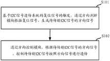
图1为本说明书实施例提供的一种基于CPLD的I2C信号透传方法的流程示意图;1 is a schematic flowchart of a CPLD-based I2C signal transparent transmission method provided by an embodiment of the present specification;
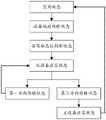
图2为本说明书实施例提供的一种方向判断模块的判断方法示意图;2 is a schematic diagram of a judgment method of a direction judgment module provided by an embodiment of the present specification;
图3为本说明书实施例提供的一种方向控制模块的电路连接示意图;FIG. 3 is a schematic diagram of circuit connection of a direction control module according to an embodiment of the present specification;
图4为本说明书实施例提供的一种基于CPLD的I2C信号透传设备的结构示意图。FIG. 4 is a schematic structural diagram of a CPLD-based I2C signal transparent transmission device according to an embodiment of the present specification.
具体实施方式Detailed ways
为了使本技术领域的人员更好地理解本说明书中的技术方案,下面将结合本说明书实施例中的附图,对本说明书实施例中的技术方案进行清楚、完整地描述,显然,所描述的实施例仅仅是本说明书一部分实施例,而不是全部的实施例。基于本说明书实施例,本领域普通技术人员在没有作出创造性劳动前提下所获得的所有其他实施例,都应当属于本说明书保护的范围。In order to make those skilled in the art better understand the technical solutions in this specification, the technical solutions in the embodiments of this specification will be clearly and completely described below with reference to the accompanying drawings in the embodiments of this specification. Obviously, the described The embodiments are only some of the embodiments of the present specification, but not all of the embodiments. Based on the embodiments of the present specification, all other embodiments obtained by persons of ordinary skill in the art without creative efforts shall fall within the protection scope of the present specification.
交换机使用支持数字诊断监控(Digital Diagnostic Monitoring,DDM)的光模块时,需要通过I2C(Inter-Integrated Circuit)总线对多个光模块进行读取操作,因为多个光模块I2C设备地址相同,所以需要多路I2C总线,分别与单个光模块通信,实际通常使用复杂可编程逻辑器件(Complex Programmable Logic Device,CPLD)进行I2C总线的扩展,将一路I2C总线扩展为多路I2C总线,选中通道后进行I2C信号的双向透传。When the switch uses an optical module that supports Digital Diagnostic Monitoring (DDM), it needs to read multiple optical modules through the I2C (Inter-Integrated Circuit) bus. Because the I2C device addresses of multiple optical modules are the same, it is necessary to Multiple I2C buses communicate with a single optical module respectively. In practice, Complex Programmable Logic Device (CPLD) is usually used to expand the I2C bus, and one I2C bus is expanded into multiple I2C buses. After selecting the channel, I2C is performed. Bidirectional transparent transmission of signals.
当前常用的I2C信号透传方法是通过CPLD分别实现一个I2C从机和一个I2C主机,I2C主机主动读取光模块DDM信息,并将读取的DDM信息存储至CPLD,由I2C从机读取DDM信息后,上报DDM信息。现有技术中的信号透传方法占用了较多的CPLD硬件资源,并且无法保证传输的实时性。The currently commonly used I2C signal transparent transmission method is to realize an I2C slave and an I2C master respectively through CPLD. The I2C master actively reads the DDM information of the optical module, and stores the read DDM information in the CPLD, and the I2C slave reads the DDM. After the information is received, report the DDM information. The signal transparent transmission method in the prior art occupies more CPLD hardware resources, and cannot guarantee the real-time transmission.
本说明书实施例提供一种基于CPLD的I2C信号透传方法,需要说明的是,本说明书书实施例中的执行主体可以是服务器,也可以是任意一种具备数据处理能力的设备。应用于I2C信号透传系统,其中,I2C信号透传系统包括设置在CPLD芯片中的方向判断模块和方向控制模块、I2C主设备以及I2C从设备,图1为本说明书实施例提供的一种基于CPLD的I2C信号透传方法的流程示意图,如图1所示,主要包括如下步骤:The embodiment of this specification provides a CPLD-based I2C signal transparent transmission method. It should be noted that the execution subject in the embodiment of this specification may be a server or any device with data processing capability. It is applied to an I2C signal transparent transmission system, wherein the I2C signal transparent transmission system includes a direction judgment module and a direction control module, an I2C master device and an I2C slave device arranged in the CPLD chip. The schematic flowchart of the I2C signal transparent transmission method of CPLD, as shown in Figure 1, mainly includes the following steps:
步骤S101,基于I2C信号透传系统的复位信号的触发,通过方向判断模块根据复位信号,生成待传输I2C信号的方向信号。Step S101 , based on the trigger of the reset signal of the I2C signal transparent transmission system, the direction judging module generates the direction signal of the I2C signal to be transmitted according to the reset signal.
其中,待传输I2C信号的方向信号用于表示待传输I2C信号的传输方向,包括第一方向和第二方向,第一方向为I2C主设备输出且I2C从设备输入的信号传输方向(MasterOut Slave In,MOSI),第二方向为I2C从设备输出且I2C主设备输入的信号传输方向(Master In Slave Out,MISO)。需要说明的是,I2C总线包括串行数据线(SDA)和串行时钟线(SCL),其中,串行数据线负责在设备间传输串行数据,串行时钟线负责产生同步时钟脉冲。Among them, the direction signal of the I2C signal to be transmitted is used to indicate the transmission direction of the I2C signal to be transmitted, including the first direction and the second direction. The first direction is the signal transmission direction output by the I2C master device and input by the I2C slave device (MasterOut Slave In , MOSI), the second direction is the signal transmission direction (Master In Slave Out, MISO) output by the I2C slave device and input by the I2C master device. It should be noted that the I2C bus includes a serial data line (SDA) and a serial clock line (SCL). The serial data line is responsible for transmitting serial data between devices, and the serial clock line is responsible for generating synchronous clock pulses.
具体地,通过该方向判断模块根据该复位信号,生成I2C信号的方向信号,具体包括:根据该复位信号,通过该方向判断模块确定该I2C信号透传系统的状态机状态,该I2C信号透传系统的状态机状态包括空闲状态、设备地址传输状态、读写标志位判断状态、从设备应答状态、第一方向数据传输状态、第二方向数据传输状态以及主设备应答状态;根据该I2C信号透传系统的状态机状态,确定该待传输I2C信号的方向信号。Specifically, the direction judging module generates the direction signal of the I2C signal according to the reset signal, which specifically includes: according to the reset signal, the state machine state of the I2C signal transparent transmission system is determined by the direction judging module, and the I2C signal is transparently transmitted. The state machine state of the system includes idle state, device address transmission state, read and write flag bit judgment state, slave device response state, first-direction data transmission state, second-direction data transmission state, and master device response state; The state machine state of the system is transmitted, and the direction signal of the I2C signal to be transmitted is determined.
在本说明书的一个实施例中,根据复位信号,通过方向判断模块确定I2C信号透传系统的状态机状态,在不同的状态下,对应的方向信号不同。需要说明的是,在本说明书的实施例中,传输方向和方向信号相同,均用于表示信号或数据的传输方向。根据I2C信号透传系统的状态机状态,确定出在当前状态机状态下,待传输I2C信号的方向信号。In an embodiment of this specification, the state machine state of the I2C signal transparent transmission system is determined by the direction determination module according to the reset signal, and in different states, the corresponding direction signals are different. It should be noted that, in the embodiments of this specification, the transmission direction and the direction signal are the same, and both are used to indicate the transmission direction of signals or data. According to the state machine state of the I2C signal transparent transmission system, the direction signal of the I2C signal to be transmitted in the current state machine state is determined.
具体地,该空闲状态用于表示该I2C信号透传系统中无信号传输的状态;该设备地址传输状态用于表示该I2C主设备向该I2C从设备依次发送指定位数的设备地址的状态;该读写标志位判断状态用于表示该I2C主设备向该I2C从设备发送读写标志位的状态;从设备应答状态用于表示该I2C从设备向该I2C主设备发送应答位或否应答位的状态;该第一方向数据传输状态用于表示该I2C主设备向该I2C从设备依次发送指定数据的状态,其中,该指定数据包括该I2C从设备的寄存器地址或待传输至该I2C从设备的寄存器中的数据;该第二方向数据传输状态用于表示该I2C从设备向该I2C主设备依次发送预设数据的状态,其中,该预设数据为待传输至该I2C主设备的寄存器中的数据;该主设备应答状态用于表示该I2C主设备向该I2从设备发送应答位或否应答位的状态。Specifically, the idle state is used to represent the state of no signal transmission in the I2C signal transparent transmission system; the device address transmission state is used to represent the state of the I2C master device sequentially sending the device address of the specified number of digits to the I2C slave device; The read-write flag bit judgment state is used to indicate the state of the I2C master device sending the read-write flag bit to the I2C slave device; the slave device response state is used to indicate that the I2C slave device sends a response bit or no response bit to the I2C master device The state of data transmission in the first direction is used to indicate the state in which the I2C master device sends specified data to the I2C slave device in turn, wherein the specified data includes the register address of the I2C slave device or to be transmitted to the I2C slave device. The data in the register; the second direction data transmission state is used to represent the state in which the I2C slave device sends preset data to the I2C master device in turn, wherein the preset data is to be transmitted to the I2C master device. data; the response status of the master device is used to indicate the status of the I2C master device sending the response bit or the no response bit to the I2 slave device.
具体地,根据该I2C信号透传系统的状态机状态,确定该待传输I2C信号的方向信号,具体包括:当该I2C信号透传系统的状态机状态为该空闲状态、该设备地址传输状态、该第一方向数据传输状态以及该主设备应答状态中的任意一种状态时,将该待传输I2C信号的方向信号确定为该第一方向。当该I2C信号透传系统的状态机状态为该读写标志位判断状态、该从设备应答状态以及该第二方向数据传输状态中的任意一种状态时,将该待传输I2C信号的方向信号确定为该第二方向。Specifically, according to the state machine state of the I2C signal transparent transmission system, determine the direction signal of the I2C signal to be transmitted, which specifically includes: when the state machine state of the I2C signal transparent transmission system is the idle state, the device address transmission state, In any state of the data transmission state in the first direction and the response state of the master device, the direction signal of the I2C signal to be transmitted is determined as the first direction. When the state machine state of the I2C signal transparent transmission system is any one of the read/write flag judgment state, the slave device response state and the second direction data transmission state, the direction signal of the I2C signal to be transmitted Determined to be the second direction.
在本说明书的一个实施例中,结合图2进行分析,图2为本说明书实施例提供的一种方向判断模块的判断方法示意图,如图2所示,系统在时钟信号的下降沿的驱动下,由复位信号进行同步复位,其中,复位信号可以是Reset信号,还可以是START信号或STOP信号,进入空闲状态。在空闲状态下,I2C信号透传系统中无信号传输,将数据位数寄存器置为7,传输方向寄存器设置为MOSI方向,也就是说第一方向,从主设备向从设备传输,并自动跳转到下一状态。空闲状态的下一状态为设备地址传输状态。In an embodiment of this specification, an analysis is made with reference to FIG. 2 , which is a schematic diagram of a judgment method of a direction judgment module provided by an embodiment of this specification. As shown in FIG. 2 , the system is driven by the falling edge of the clock signal. , synchronous reset is performed by a reset signal, wherein the reset signal may be a Reset signal, or a START signal or a STOP signal to enter an idle state. In the idle state, there is no signal transmission in the I2C signal transparent transmission system, the data bit register is set to 7, and the transmission direction register is set to the MOSI direction, that is to say, the first direction is to transmit from the master device to the slave device, and automatically jump Go to the next state. The next state of the idle state is the device address transfer state.
在设备地址传输状态下,传输方向为MOSI方向,以便于主设备向从设备发送设备地址。当接收到时钟信号的下降沿时,主设备向从设备依次发送从设备的设备地址的前七位,每接收一位设备地址,将数据位数寄存器递减一位,直至数据位数寄存器为0。当数据位数寄存器为0时,跳转到读写标志位判断状态,并将传输方向寄存器设置为MISO方向。In the device address transmission state, the transmission direction is the MOSI direction, so that the master device can send the device address to the slave device. When receiving the falling edge of the clock signal, the master device sends the first seven bits of the device address of the slave device to the slave device in turn, and for each bit of the device address received, the data bit register is decremented by one bit until the data bit register is 0 . When the data bit register is 0, jump to the read/write flag bit judgment state, and set the transfer direction register to the MISO direction.
在读写标志位判断状态下,表示主设备向从设备发送读写标志位的状态,判断当前SDA信号中的最后一位,也就是设备地址的最低位,当最低位为1时,代表读状态,当最低位为0时,表示写状态。将设备地址的最低位锁存在命令寄存器中,此状态下传输方向仍为MISO方向,并跳转至从设备应答状态。In the read-write flag bit judgment state, it indicates the state of the master device sending the read-write flag bit to the slave device, and judges the last bit in the current SDA signal, which is the lowest bit of the device address. When the lowest bit is 1, it means read Status, when the lowest bit is 0, it means write status. The lowest bit of the device address is latched in the command register. In this state, the transmission direction is still the MISO direction, and it jumps to the slave device response state.
在从设备应答状态下,传输方向仍为MISO方向,以便于从设备向主设备发送应答位或否应答位,并将数据位数寄存器设置为7。此时,根据命令寄存器中存储的读写标志位,确定下一状态。In the response state of the slave device, the transmission direction is still the MISO direction, so that the slave device can send the response bit or no response bit to the master device, and the data bit register is set to 7. At this time, the next state is determined according to the read and write flag bits stored in the command register.
当命令寄存器中存储的读写标志位为0时,进入第一方向数据传输状态,也就是在下一状态下,主设备向从设备发送数据,此处的数据可以是寄存器数据,也可以是待传输的数据。在此状态下,传输方向为MOSI方向。在时钟信号下降沿的驱动下,主设备依次向从设备发送数据,每发送一次将数据位数寄存器减一,直至数据位数寄存器为0时,将传输方向转变为MISO方向,进入从设备应答状态。在从设备应答状态下传输方向为MISO方向,以便于从设备根据接收到的数据向主设备发送应答位或否应答位,当主设备接收到应答位之后,此处数据传输完成。When the read-write flag bit stored in the command register is 0, it enters the first-direction data transmission state, that is, in the next state, the master device sends data to the slave device, and the data here can be register data or pending transmitted data. In this state, the transmission direction is the MOSI direction. Driven by the falling edge of the clock signal, the master device sends data to the slave device in turn, and the data bit register is decremented by one each time it is sent. When the data bit register is 0, the transmission direction is changed to the MISO direction, and the slave device responds. state. In the response state of the slave device, the transmission direction is the MISO direction, so that the slave device can send the response bit or no response bit to the master device according to the received data. After the master device receives the response bit, the data transmission is completed here.
当命令寄存器中存储的读写标志位为1时,进入第二方向数据传输状态,也就是在下一状态下,从设备向主设备发送数据,在此状态下,传输方向为MISO方向。在时钟信号下降沿的驱动下,从设备依次向主设备发送数据,每发送一次将数据位数寄存器减一,直至数据位数寄存器为0时,将传输方向转变为MOSI方向,进入主设备应答状态。在主设备应答状态下传输方向为MOSI方向,以便于主设备根据接收到的数据向从设备发送应答位或否应答位。若从设备接收到应答位,则继续进行字节传输,若从设备接收到否应答位,则结束传输。在主设备应答状态下,读取串行数据线的电平,并锁存至sda_bit中,当sda_bit为1时,将传输方向设置为MOSI方向,并跳转至空闲状态;当sda_bit为0时,将传输方向设置为MISO方向,并将数据位置寄存器置为7,跳转至第一方向传输状态。When the read-write flag bit stored in the command register is 1, it enters the second-direction data transmission state, that is, in the next state, the slave device sends data to the master device. In this state, the transmission direction is the MISO direction. Driven by the falling edge of the clock signal, the slave device sends data to the master device in turn, and the data bit register is decremented by one each time it is sent. When the data bit register is 0, the transmission direction is changed to the MOSI direction, and the master device responds. state. In the master device's response state, the transmission direction is the MOSI direction, so that the master device can send a response bit or no response bit to the slave device according to the received data. If the slave device receives the acknowledge bit, it will continue the byte transmission, and if the slave device receives the no acknowledge bit, it will end the transfer. In the master response state, read the level of the serial data line and latch it into sda_bit. When sda_bit is 1, set the transmission direction to MOSI direction and jump to the idle state; when sda_bit is 0 , set the transfer direction to the MISO direction, and set the data location register to 7, and jump to the first direction transfer state.
步骤S102,通过方向控制模块,根据待传输I2C信号的方向信号,控制待传输I2C信号按照方向信号进行透传。Step S102 , through the direction control module, according to the direction signal of the I2C signal to be transmitted, the I2C signal to be transmitted is controlled to be transparently transmitted according to the direction signal.
在本说明书的一个实施例中,根据状态机的状态不同,生成的待传输I2C信号的方向信号不同。根据不同状态下对应的方向信号,实现主设备和从设备之间按照方向信号进行数据信号的透传。In an embodiment of this specification, according to different states of the state machine, the generated direction signals of the I2C signal to be transmitted are different. According to the corresponding direction signals in different states, the transparent transmission of data signals between the master device and the slave device according to the direction signals is realized.
具体地,方向控制模块包括:第一反相器、第一三态缓冲器、第二三态缓冲器、第一缓冲器以及第二缓冲器;其中,该第一反相器的输入端用于输入该方向信号,该第一反相器的输出端与该第一三态缓冲器的选项卡通输入端相连;该第一三态缓冲器的输入端用于接收该第二缓冲器的输出端的信号,该第一三态缓冲器的输出端与该I2C主设备相连;该第一缓冲器的输入端用于输入该I2C主设备的待传输I2C信号,该第一缓冲器的输出端与该第二三态缓冲器的输入端相连;该第二三态缓冲器的选项卡通输入端用于输入该方向信号,该第二三态的输出端与该I2C从设备相连;该第二缓冲器的输入端用于输入该I2C从设备的待传输I2C信号。Specifically, the direction control module includes: a first inverter, a first tri-state buffer, a second tri-state buffer, a first buffer and a second buffer; wherein, the input end of the first inverter is For inputting the direction signal, the output end of the first inverter is connected to the option card input end of the first tri-state buffer; the input end of the first tri-state buffer is used to receive the output of the second buffer The output end of the first three-state buffer is connected to the I2C master device; the input end of the first buffer is used to input the I2C signal to be transmitted by the I2C master device, and the output end of the first buffer is connected to the I2C master device. The input end of the second tri-state buffer is connected; the option card input end of the second tri-state buffer is used to input the direction signal, and the output end of the second tri-state buffer is connected with the I2C slave device; the second buffer The input terminal of the device is used to input the I2C signal to be transmitted from the I2C slave device.
通过该方向控制模块,根据该待传输I2C信号的方向信号,控制该待传输I2C信号按照该方向信号进行透传,具体包括:将该待传输I2C信号的方向信号输入至该第一反相器的输入端和该第二三态缓冲器的选项卡通输入端;根据该待传输I2C信号的方向信号,确定出该第一三态缓冲器和该第二三态缓冲器的工作状态;根据该第一三态缓冲器和该第二三态缓冲器的工作状态,生成该I2C主设备与该I2C从设备之间的透传路线。Through the direction control module, according to the direction signal of the I2C signal to be transmitted, the I2C signal to be transmitted is controlled to be transparently transmitted according to the direction signal, which specifically includes: inputting the direction signal of the I2C signal to be transmitted to the first inverter. The input end of the second tri-state buffer and the option card input end of the second tri-state buffer; according to the direction signal of the I2C signal to be transmitted, determine the working state of the first tri-state buffer and the second tri-state buffer; according to the The working states of the first tri-state buffer and the second tri-state buffer generate a transparent transmission route between the I2C master device and the I2C slave device.
具体地,根据该待传输I2C信号的方向信号,确定出该第一三态缓冲器和该第二三态缓冲器的工作状态,具体包括:当该待传输I2C信号的方向信号为该第一方向时,该第一三态缓冲器为禁能状态,其中,在该禁能状态下该第一三态缓冲器的输出端为高阻态;当该待传输I2C信号的方向信号为该第二方向时,该第二三态缓冲器为禁能状态,其中,在该禁能状态下该第二三态缓冲器的输出端为高阻态。Specifically, determining the working states of the first tri-state buffer and the second tri-state buffer according to the direction signal of the I2C signal to be transmitted, which specifically includes: when the direction signal of the I2C signal to be transmitted is the first tri-state buffer direction, the first tri-state buffer is in a disabled state, wherein, in the disabled state, the output end of the first tri-state buffer is in a high-impedance state; when the direction signal of the I2C signal to be transmitted is the third In two directions, the second tri-state buffer is in a disabled state, wherein in the disabled state, the output end of the second tri-state buffer is in a high impedance state.
具体地,根据该第一三态缓冲器和该第二三态缓冲器的工作状态,生成该I2C主设备与该I2C从设备之间的透传路线,具体包括:当该第一三态缓冲器为禁能状态时,该I2C主设备与该I2C从设备之间的透传路线为:该I2C主设备的该待传输I2C信号输入至该第一缓冲器的输入端,通过该第一缓冲器的输出端输出该待传输I2C信号,并将该待传输I2C信号输入至该第二三态缓冲器的输入端,通过该第二三态缓冲器的输出端输出至该I2C从设备;当该第二三态缓冲器为禁能状态时,该I2C从设备与该I2C主设备之间的透传路线为:该I2C从设备的该待传输I2C信号输入至该第二缓冲器的输入端,通过该第二缓冲器的输出端输出该待传输I2C信号,并将该待传输I2C信号输入至该第一三态缓冲器的输入端,通过该第一三态缓冲器的输出端输出至该I2C主设备。Specifically, generating a transparent transmission route between the I2C master device and the I2C slave device according to the working states of the first tristate buffer and the second tristate buffer, specifically including: when the first tristate buffer When the device is in the disabled state, the transparent transmission route between the I2C master device and the I2C slave device is as follows: the I2C signal to be transmitted of the I2C master device is input to the input end of the first buffer, through the first buffer The output terminal of the device outputs the I2C signal to be transmitted, and the I2C signal to be transmitted is input to the input terminal of the second three-state buffer, and is output to the I2C slave device through the output terminal of the second three-state buffer; when When the second tri-state buffer is in the disabled state, the transparent transmission route between the I2C slave device and the I2C master device is: the I2C signal to be transmitted of the I2C slave device is input to the input end of the second buffer , output the I2C signal to be transmitted through the output terminal of the second buffer, input the I2C signal to be transmitted to the input terminal of the first tri-state buffer, and output the I2C signal to the input terminal of the first tri-state buffer through the output terminal of the first tri-state buffer. the I2C master device.
在本说明书的一个实施例中,图3为本说明书实施例提供的一种方向控制模块的电路连接示意图,如图3所示,方向控制模块的电路包括第一反相器N1、第一三态缓冲器TR1、第二三态缓冲器TR2、第一缓冲器BF1以及第二缓冲器BF2。其中,方向信号输入之后,一路进入第二三态缓冲器TR2的ENB引脚,也就是说选项卡通输入端;另一路方向信号经过第一反相器N1后输入第一三态缓冲器TR1的ENB引脚。第一三态缓冲器TR1的输出接主设备信号,第二三态缓冲器TR2的输出接从设备信号。主设备信号经过第一缓冲器BF1后接第二三态缓冲器TR2的输入引脚;从设备信号经第二缓冲器BF2后接第一三态缓冲器TR1的输入引脚。In an embodiment of the present specification, FIG. 3 is a schematic diagram of circuit connection of a direction control module provided by an embodiment of the present specification. As shown in FIG. 3 , the circuit of the direction control module includes a first inverter N1, a first three A state buffer TR1, a second tri-state buffer TR2, a first buffer BF1, and a second buffer BF2. Among them, after the direction signal is input, one way enters the ENB pin of the second tri-state buffer TR2, that is, the input terminal of the option card; the other way of the direction signal passes through the first inverter N1 and then enters the first tri-state buffer TR1. ENB pin. The output of the first three-state buffer TR1 is connected to the signal of the master device, and the output of the second three-state buffer TR2 is connected to the signal of the slave device. The master device signal is connected to the input pin of the second tri-state buffer TR2 after passing through the first buffer BF1; the slave device signal is connected to the input pin of the first tri-state buffer TR1 after passing through the second buffer BF2.
当方向信号为MOSI方向,即高电平1时,第一三态缓冲器TR1的使能引脚ENB为低,第一三态缓冲器TR1禁能,此时第一三态缓冲器TR1输出高阻态。主设备信号经第一缓冲器BF1进入第二三态缓冲器TR2的输入端,此时第二三态缓冲器TR2的使能引脚ENB为高电平,第二三态缓冲器TR2使能,输入信号为主设备信号,输出信号为从设备信号,输出信号等于输入信号,实现主机到从机的透传。When the direction signal is the MOSI direction, that is, the high level is 1, the enable pin ENB of the first tri-state buffer TR1 is low, and the first tri-state buffer TR1 is disabled. At this time, the first tri-state buffer TR1 outputs high impedance state. The master device signal enters the input end of the second tri-state buffer TR2 through the first buffer BF1. At this time, the enable pin ENB of the second tri-state buffer TR2 is at a high level, and the second tri-state buffer TR2 is enabled. , the input signal is the master device signal, the output signal is the slave device signal, the output signal is equal to the input signal, and the transparent transmission from the master device to the slave device is realized.
当方向信号为MISO方向,即低电平0时,第二三态缓冲器TR2的使能引脚ENB为低,第二三态缓冲器TR2禁能,此时第二三态缓冲器TR2输出高阻态。从设备信号经第二缓冲器BF2进入第一三态缓冲器TR1的输入端,此时第一三态缓冲器TR1的使能引脚ENB为低电平,第一三态缓冲器TR1使能,输出信号为主设备信号,输入信号为从设备信号,输出信号等于输入信号,实现从机到主机的透传。When the direction signal is the MISO direction, that is, the low level is 0, the enable pin ENB of the second tri-state buffer TR2 is low, and the second tri-state buffer TR2 is disabled. At this time, the second tri-state buffer TR2 outputs high impedance state. The signal from the device enters the input end of the first tri-state buffer TR1 through the second buffer BF2. At this time, the enable pin ENB of the first tri-state buffer TR1 is at a low level, and the first tri-state buffer TR1 is enabled. , the output signal is the master device signal, the input signal is the slave device signal, the output signal is equal to the input signal, and the transparent transmission from the slave to the master is realized.
通过上述技术方案,CPLD仅用于传输,无需将数据进行存储后再读取,节省了CPLD的硬件资源,并且保证了信号传输的实时性。Through the above technical solution, the CPLD is only used for transmission, and there is no need to store and then read the data, which saves the hardware resources of the CPLD and ensures the real-time nature of signal transmission.
本说明书实施例还提供一种基于CPLD的I2C信号透传设备,如图4所示,设备包括:至少一个处理器;以及,与至少一个处理器通信连接的存储器;其中,存储器存储有可被至少一个处理器执行的指令,指令被至少一个处理器执行,以使至少一个处理器能够:基于I2C信号透传系统的复位信号的触发,通过方向判断模块根据所述复位信号,生成待传输I2C信号的方向信号;其中,待传输I2C信号的方向信号用于表示待传输I2C信号的传输方向,包括第一方向和第二方向,第一方向为I2C主设备输出且I2C从设备输入的信号传输方向,第二方向为I2C从设备输出且I2C主设备输入的信号传输方向;通过方向控制模块,根据待传输I2C信号的方向信号,控制待传输I2C信号按照方向信号进行透传。The embodiments of this specification also provide a CPLD-based I2C signal transparent transmission device. As shown in FIG. 4 , the device includes: at least one processor; and a memory communicatively connected to the at least one processor; The instruction executed by at least one processor, the instruction is executed by at least one processor, so that the at least one processor can: based on the trigger of the reset signal of the I2C signal transparent transmission system, generate the I2C to be transmitted according to the reset signal through the direction judging module The direction signal of the signal; wherein, the direction signal of the I2C signal to be transmitted is used to indicate the transmission direction of the I2C signal to be transmitted, including the first direction and the second direction. The first direction is the signal transmission output by the I2C master device and input by the I2C slave device. The second direction is the signal transmission direction output by the I2C slave device and input by the I2C master device; through the direction control module, according to the direction signal of the I2C signal to be transmitted, the I2C signal to be transmitted is controlled to be transparently transmitted according to the direction signal.
本说明书实施例还提供一种非易失性计算机存储介质,存储有计算机可执行指令,计算机可执行指令设置为:The embodiments of this specification also provide a non-volatile computer storage medium, which stores computer-executable instructions, and the computer-executable instructions are set to:
基于I2C信号透传系统的复位信号的触发,通过方向判断模块根据所述复位信号,生成待传输I2C信号的方向信号;其中,待传输I2C信号的方向信号用于表示待传输I2C信号的传输方向,包括第一方向和第二方向,第一方向为I2C主设备输出且I2C从设备输入的信号传输方向,第二方向为I2C从设备输出且I2C主设备输入的信号传输方向;通过方向控制模块,根据待传输I2C信号的方向信号,控制待传输I2C信号按照方向信号进行透传。Based on the trigger of the reset signal of the I2C signal transparent transmission system, the direction judging module generates the direction signal of the I2C signal to be transmitted according to the reset signal; wherein, the direction signal of the I2C signal to be transmitted is used to indicate the transmission direction of the I2C signal to be transmitted. , including the first direction and the second direction, the first direction is the signal transmission direction output by the I2C master device and input by the I2C slave device, and the second direction is the signal transmission direction output by the I2C slave device and input by the I2C master device; through the direction control module , according to the direction signal of the I2C signal to be transmitted, control the I2C signal to be transmitted to be transparently transmitted according to the direction signal.
本说明书中的各个实施例均采用递进的方式描述,各个实施例之间相同相似的部分互相参见即可,每个实施例重点说明的都是与其他实施例的不同之处。尤其,对于装置、设备、非易失性计算机存储介质实施例而言,由于其基本相似于方法实施例,所以描述的比较简单,相关之处参见方法实施例的部分说明即可。Each embodiment in this specification is described in a progressive manner, and the same and similar parts between the various embodiments may be referred to each other, and each embodiment focuses on the differences from other embodiments. In particular, for the apparatus, equipment, and non-volatile computer storage medium embodiments, since they are basically similar to the method embodiments, the description is relatively simple, and reference may be made to some descriptions of the method embodiments for related parts.
上述对本说明书特定实施例进行了描述。其它实施例在所附权利要求书的范围内。在一些情况下,在权利要求书中记载的动作或步骤可以按照不同于实施例中的顺序来执行并且仍然可以实现期望的结果。另外,在附图中描绘的过程不一定要求示出的特定顺序或者连续顺序才能实现期望的结果。在某些实施方式中,多任务处理和并行处理也是可以的或者可能是有利的。The foregoing describes specific embodiments of the present specification. Other embodiments are within the scope of the appended claims. In some cases, the actions or steps recited in the claims can be performed in an order different from that in the embodiments and still achieve desirable results. Additionally, the processes depicted in the figures do not necessarily require the particular order shown, or sequential order, to achieve desirable results. In some embodiments, multitasking and parallel processing are also possible or may be advantageous.
以上该仅为本说明书的一个或多个实施例而已,并不用于限制本说明书。对于本领域技术人员来说,本说明书的一个或多个实施例可以有各种更改和变化。凡在本说明书的一个或多个实施例的精神和原理之内所作的任何修改、等同替换、改进等,均应包含在本说明书的权利要求范围之内。The above are only one or more embodiments of the present specification, and are not intended to limit the present specification. Various modifications and variations of the one or more embodiments of this specification are possible for those skilled in the art. Any modification, equivalent replacement, improvement, etc. made within the spirit and principle of one or more embodiments of this specification should be included within the scope of the claims of this specification.
Claims (10)
Priority Applications (1)
| Application Number | Priority Date | Filing Date | Title |
|---|---|---|---|
| CN202210404241.7ACN114925013B (en) | 2022-04-18 | 2022-04-18 | A method, device and medium for I2C signal transparent transmission based on CPLD |
Applications Claiming Priority (1)
| Application Number | Priority Date | Filing Date | Title |
|---|---|---|---|
| CN202210404241.7ACN114925013B (en) | 2022-04-18 | 2022-04-18 | A method, device and medium for I2C signal transparent transmission based on CPLD |
Publications (2)
| Publication Number | Publication Date |
|---|---|
| CN114925013Atrue CN114925013A (en) | 2022-08-19 |
| CN114925013B CN114925013B (en) | 2025-02-07 |
Family
ID=82806814
Family Applications (1)
| Application Number | Title | Priority Date | Filing Date |
|---|---|---|---|
| CN202210404241.7AActiveCN114925013B (en) | 2022-04-18 | 2022-04-18 | A method, device and medium for I2C signal transparent transmission based on CPLD |
Country Status (1)
| Country | Link |
|---|---|
| CN (1) | CN114925013B (en) |
Cited By (2)
| Publication number | Priority date | Publication date | Assignee | Title |
|---|---|---|---|---|
| CN115630011A (en)* | 2022-10-27 | 2023-01-20 | 东莞记忆存储科技有限公司 | Method and device for realizing I2C bus communication of master and slave equipment by using CPLD |
| CN119781581A (en)* | 2025-03-07 | 2025-04-08 | 湖南国科超算科技有限公司 | CPU synchronization system and method based on double CPLD bidirectional control |
Citations (13)
| Publication number | Priority date | Publication date | Assignee | Title |
|---|---|---|---|---|
| KR20050011822A (en)* | 2003-07-24 | 2005-01-31 | 삼성전자주식회사 | Apparatus for connecting plurality of device with same address to one bus controller and operation method thereof |
| CN1926792A (en)* | 2004-03-05 | 2007-03-07 | 菲尼萨公司 | Integrated Post Amplifier, Laser Driver and Controller |
| CN101158932A (en)* | 2007-08-31 | 2008-04-09 | 上海广电(集团)有限公司中央研究院 | Method for accessing on-site programmable gate array internal memory through I*C interface |
| US20090119439A1 (en)* | 2007-11-02 | 2009-05-07 | Inventec Corporation | Structure compatible with i2c bus and system management bus and timing buffering apparatus thereof |
| US20110316581A1 (en)* | 2010-06-24 | 2011-12-29 | Oki Semiconductor Co., Ltd | Semiconductor device with bus connection circuit and method of making bus connection |
| CN103714029A (en)* | 2013-05-07 | 2014-04-09 | 深圳市汇春科技有限公司 | Novel two-line synchronous communication protocol and application |
| US20160278141A1 (en)* | 2015-03-18 | 2016-09-22 | Lattice Semiconductor Corporation | Embedding Low-Speed Communications In A High Speed Wireless Tunneling System |
| CN107562668A (en)* | 2017-08-31 | 2018-01-09 | 广东欧珀移动通信有限公司 | Bus deadlock recovery system and method |
| CN109446145A (en)* | 2018-10-30 | 2019-03-08 | 郑州云海信息技术有限公司 | A kind of channel server master board I2C extended chip, circuit and control method |
| CN209657808U (en)* | 2019-04-08 | 2019-11-19 | 苏州汇峰微电子有限公司 | A kind of dynamic RAM data transmission channel |
| CN110784285A (en)* | 2019-10-12 | 2020-02-11 | 深圳思凯微电子有限公司 | Transparent transmission data structure protection method, device, equipment and storage medium |
| US20210265001A1 (en)* | 2020-02-26 | 2021-08-26 | Realtek Semiconductor Corporation | Method of testing slave device of Inter-Integrated Circuit bus |
| CN114253898A (en)* | 2021-12-27 | 2022-03-29 | 上海集成电路研发中心有限公司 | Bus device and data read-write circuit |
- 2022
- 2022-04-18CNCN202210404241.7Apatent/CN114925013B/enactiveActive
Patent Citations (13)
| Publication number | Priority date | Publication date | Assignee | Title |
|---|---|---|---|---|
| KR20050011822A (en)* | 2003-07-24 | 2005-01-31 | 삼성전자주식회사 | Apparatus for connecting plurality of device with same address to one bus controller and operation method thereof |
| CN1926792A (en)* | 2004-03-05 | 2007-03-07 | 菲尼萨公司 | Integrated Post Amplifier, Laser Driver and Controller |
| CN101158932A (en)* | 2007-08-31 | 2008-04-09 | 上海广电(集团)有限公司中央研究院 | Method for accessing on-site programmable gate array internal memory through I*C interface |
| US20090119439A1 (en)* | 2007-11-02 | 2009-05-07 | Inventec Corporation | Structure compatible with i2c bus and system management bus and timing buffering apparatus thereof |
| US20110316581A1 (en)* | 2010-06-24 | 2011-12-29 | Oki Semiconductor Co., Ltd | Semiconductor device with bus connection circuit and method of making bus connection |
| CN103714029A (en)* | 2013-05-07 | 2014-04-09 | 深圳市汇春科技有限公司 | Novel two-line synchronous communication protocol and application |
| US20160278141A1 (en)* | 2015-03-18 | 2016-09-22 | Lattice Semiconductor Corporation | Embedding Low-Speed Communications In A High Speed Wireless Tunneling System |
| CN107562668A (en)* | 2017-08-31 | 2018-01-09 | 广东欧珀移动通信有限公司 | Bus deadlock recovery system and method |
| CN109446145A (en)* | 2018-10-30 | 2019-03-08 | 郑州云海信息技术有限公司 | A kind of channel server master board I2C extended chip, circuit and control method |
| CN209657808U (en)* | 2019-04-08 | 2019-11-19 | 苏州汇峰微电子有限公司 | A kind of dynamic RAM data transmission channel |
| CN110784285A (en)* | 2019-10-12 | 2020-02-11 | 深圳思凯微电子有限公司 | Transparent transmission data structure protection method, device, equipment and storage medium |
| US20210265001A1 (en)* | 2020-02-26 | 2021-08-26 | Realtek Semiconductor Corporation | Method of testing slave device of Inter-Integrated Circuit bus |
| CN114253898A (en)* | 2021-12-27 | 2022-03-29 | 上海集成电路研发中心有限公司 | Bus device and data read-write circuit |
Cited By (2)
| Publication number | Priority date | Publication date | Assignee | Title |
|---|---|---|---|---|
| CN115630011A (en)* | 2022-10-27 | 2023-01-20 | 东莞记忆存储科技有限公司 | Method and device for realizing I2C bus communication of master and slave equipment by using CPLD |
| CN119781581A (en)* | 2025-03-07 | 2025-04-08 | 湖南国科超算科技有限公司 | CPU synchronization system and method based on double CPLD bidirectional control |
Also Published As
| Publication number | Publication date |
|---|---|
| CN114925013B (en) | 2025-02-07 |
Similar Documents
| Publication | Publication Date | Title |
|---|---|---|
| JP7247213B2 (en) | debug controller circuit | |
| US4961140A (en) | Apparatus and method for extending a parallel synchronous data and message bus | |
| US6968472B2 (en) | Serial data interface | |
| TW200530822A (en) | Serial peripheral interface (SPI) apparatus with write buffer for improving data throughput | |
| EP0329776A1 (en) | Method and apparatus for interconnecting busses in a multibus computer system | |
| JPH0778773B2 (en) | Communication device and method of using the communication device | |
| US20070240011A1 (en) | FIFO memory data pipelining system and method for increasing I²C bus speed | |
| US10896119B1 (en) | Common input/output interface for application and debug circuitry | |
| CN114925013A (en) | CPLD-based I2C signal transparent transmission method, device and medium | |
| CN106469127B (en) | A data access device and method | |
| US10409749B2 (en) | Semiconductor device and system provided with a communication interface | |
| CN114265872A (en) | Interconnection device for bus | |
| US20240264961A1 (en) | System and method for optimizing ahb bus data transmission performance and server | |
| JP2000242573A (en) | Method and device for connecting manufacture test interface to global serial bus including i2c bus | |
| CN105790830A (en) | Optical module in-situ detection method and device | |
| CN104834620A (en) | SPI (serial peripheral interface) bus circuit, realization method and electronic equipment | |
| US6263393B1 (en) | Bus switch for realizing bus transactions across two or more buses | |
| CN113434442B (en) | A switch and data access method | |
| CN118467434B (en) | Service system, input and output chassis, equipment chassis and chassis identification method | |
| JPH07123260B2 (en) | Circuit and method for capturing and verifying data from an asynchronous Micro Channel bus | |
| US6874043B2 (en) | Data buffer | |
| CN116340217A (en) | Data processing method and related device | |
| JP2589821B2 (en) | Central processing unit of information processing system | |
| CN115658415A (en) | A chip debugging device and method | |
| US7206889B2 (en) | Systems and methods for enabling communications among devices in a multi-cache line size environment and disabling communications among devices of incompatible cache line sizes |
Legal Events
| Date | Code | Title | Description |
|---|---|---|---|
| PB01 | Publication | ||
| PB01 | Publication | ||
| SE01 | Entry into force of request for substantive examination | ||
| SE01 | Entry into force of request for substantive examination | ||
| CB02 | Change of applicant information | ||
| CB02 | Change of applicant information | Country or region after:China Address after:250101 s01-6 / F, No. 1036, Langchao Road, high tech Zone, Jinan City, Shandong Province Applicant after:Inspur Network Technology (Shandong) Co.,Ltd. Address before:250101 s01-6 / F, No. 1036, Langchao Road, high tech Zone, Jinan City, Shandong Province Applicant before:INSPUR CISCO NETWORK TECHNOLOGY Co.,Ltd. Country or region before:China | |
| GR01 | Patent grant | ||
| GR01 | Patent grant |