CN114878919A - Quality factor detection circuit and method based on oscillation circuit and electronic equipment - Google Patents
Quality factor detection circuit and method based on oscillation circuit and electronic equipmentDownload PDFInfo
- Publication number
- CN114878919A CN114878919ACN202210307078.2ACN202210307078ACN114878919ACN 114878919 ACN114878919 ACN 114878919ACN 202210307078 ACN202210307078 ACN 202210307078ACN 114878919 ACN114878919 ACN 114878919A
- Authority
- CN
- China
- Prior art keywords
- switch
- switch assembly
- capacitor
- circuit
- switch component
- Prior art date
- Legal status (The legal status is an assumption and is not a legal conclusion. Google has not performed a legal analysis and makes no representation as to the accuracy of the status listed.)
- Pending
Links
Images


Classifications
- H—ELECTRICITY
- H02—GENERATION; CONVERSION OR DISTRIBUTION OF ELECTRIC POWER
- H02J—CIRCUIT ARRANGEMENTS OR SYSTEMS FOR SUPPLYING OR DISTRIBUTING ELECTRIC POWER; SYSTEMS FOR STORING ELECTRIC ENERGY
- H02J50/00—Circuit arrangements or systems for wireless supply or distribution of electric power
- H02J50/10—Circuit arrangements or systems for wireless supply or distribution of electric power using inductive coupling
- H02J50/12—Circuit arrangements or systems for wireless supply or distribution of electric power using inductive coupling of the resonant type
- G—PHYSICS
- G01—MEASURING; TESTING
- G01R—MEASURING ELECTRIC VARIABLES; MEASURING MAGNETIC VARIABLES
- G01R27/00—Arrangements for measuring resistance, reactance, impedance, or electric characteristics derived therefrom
- G01R27/02—Measuring real or complex resistance, reactance, impedance, or other two-pole characteristics derived therefrom, e.g. time constant
- G01R27/26—Measuring inductance or capacitance; Measuring quality factor, e.g. by using the resonance method; Measuring loss factor; Measuring dielectric constants ; Measuring impedance or related variables
- G01R27/2688—Measuring quality factor or dielectric loss, e.g. loss angle, or power factor
- G01R27/2694—Measuring dielectric loss, e.g. loss angle, loss factor or power factor
- H—ELECTRICITY
- H02—GENERATION; CONVERSION OR DISTRIBUTION OF ELECTRIC POWER
- H02J—CIRCUIT ARRANGEMENTS OR SYSTEMS FOR SUPPLYING OR DISTRIBUTING ELECTRIC POWER; SYSTEMS FOR STORING ELECTRIC ENERGY
- H02J50/00—Circuit arrangements or systems for wireless supply or distribution of electric power
- H02J50/60—Circuit arrangements or systems for wireless supply or distribution of electric power responsive to the presence of foreign objects, e.g. detection of living beings
- H—ELECTRICITY
- H02—GENERATION; CONVERSION OR DISTRIBUTION OF ELECTRIC POWER
- H02J—CIRCUIT ARRANGEMENTS OR SYSTEMS FOR SUPPLYING OR DISTRIBUTING ELECTRIC POWER; SYSTEMS FOR STORING ELECTRIC ENERGY
- H02J50/00—Circuit arrangements or systems for wireless supply or distribution of electric power
- H02J50/80—Circuit arrangements or systems for wireless supply or distribution of electric power involving the exchange of data, concerning supply or distribution of electric power, between transmitting devices and receiving devices
- Y—GENERAL TAGGING OF NEW TECHNOLOGICAL DEVELOPMENTS; GENERAL TAGGING OF CROSS-SECTIONAL TECHNOLOGIES SPANNING OVER SEVERAL SECTIONS OF THE IPC; TECHNICAL SUBJECTS COVERED BY FORMER USPC CROSS-REFERENCE ART COLLECTIONS [XRACs] AND DIGESTS
- Y02—TECHNOLOGIES OR APPLICATIONS FOR MITIGATION OR ADAPTATION AGAINST CLIMATE CHANGE
- Y02B—CLIMATE CHANGE MITIGATION TECHNOLOGIES RELATED TO BUILDINGS, e.g. HOUSING, HOUSE APPLIANCES OR RELATED END-USER APPLICATIONS
- Y02B70/00—Technologies for an efficient end-user side electric power management and consumption
- Y02B70/10—Technologies improving the efficiency by using switched-mode power supplies [SMPS], i.e. efficient power electronics conversion e.g. power factor correction or reduction of losses in power supplies or efficient standby modes
Landscapes
- Engineering & Computer Science (AREA)
- Power Engineering (AREA)
- Computer Networks & Wireless Communication (AREA)
- Physics & Mathematics (AREA)
- General Physics & Mathematics (AREA)
- Inductance-Capacitance Distribution Constants And Capacitance-Resistance Oscillators (AREA)
- Dc-Dc Converters (AREA)
- Charge And Discharge Circuits For Batteries Or The Like (AREA)
Abstract
Translated fromChinese
Description
Translated fromChinese本申请是分案申请,原申请的申请号是202010463813.X,原申请日是2020年05月27日,原申请的全部内容通过引用结合在本申请中。This application is a divisional application, the application number of the original application is 202010463813.X, the original application date is May 27, 2020, and the entire content of the original application is incorporated into this application by reference.
技术领域technical field
本申请涉及电子技术领域,尤其涉及一种基于振荡电路的品质因子检测电路、检测方法及电子设备。The present application relates to the field of electronic technology, and in particular, to a quality factor detection circuit, a detection method and an electronic device based on an oscillator circuit.
背景技术Background technique
随着无线充电技术的普及,市场上涌现出许多无线充电产品,其中以基于无线充电联盟(wireless power consortium,WPC)Qi标准的手机发射端占有率为最大。With the popularization of wireless charging technology, many wireless charging products have emerged in the market, among which mobile phone transmitters based on the wireless power consortium (wireless power consortium, WPC) Qi standard have the largest share.
在无线充电产品应用中,无线充电产品通常处于一个开放的场景中,例如:具有无线充电功能的手机使用作为附件的充电器进行充电,手机和充电器是独立的可分离的产品形式。附件中的发送(transport,TX)装置需要对放入附件的接收(receive,RX)装置(通常安装在手机等具有无线充电功能的电子设备内部)进行实时检测和识别,当识别到接收装置则开始控制充电完成电能传输。同时,也需要判断发送装置和接收装置之间是否有异物,如果不能精确检测异物,就会存在充电过程中损坏异物(比如银行卡、身份证等)的场景,这严重制约着无线充电行业的发展,也正因此异物检测成为无线充电安全的首要问题,也是业界痛点。In the application of wireless charging products, wireless charging products are usually in an open scenario. For example, a mobile phone with wireless charging function is charged with a charger as an accessory, and the mobile phone and the charger are independent and separable product forms. The transmitting (transport, TX) device in the accessory needs to perform real-time detection and identification of the receiving (receive, RX) device (usually installed inside an electronic device with wireless charging function such as a mobile phone) placed in the accessory. Start to control the charging to complete the power transfer. At the same time, it is also necessary to judge whether there is a foreign object between the sending device and the receiving device. If the foreign object cannot be accurately detected, there will be a scene where foreign objects (such as bank cards, ID cards, etc.) are damaged during the charging process, which seriously restricts the wireless charging industry. Development, and therefore foreign object detection has become the primary issue of wireless charging safety, and it is also a pain point in the industry.
而当前无线充电异物检测能力有限,覆盖范围小,很多异物无法检测到,严重威胁着无线充电的安全,对行业的进一步发展极其不利。目前,采用的异物检测方法主要为品质因子(quality factor,Q)值检测法。其中,Q值检测法的原理是:发送装置和接收装置之间存在异物时,会影响发送装置的电感线圈的参数进而影响到电感线圈的Q值,从而通过检测电感线圈的Q值可以反应是否存在异物。所以提高Q值的检测精度和检测速度可以提高异物检测的准确性,因此,如何快速高精度的检测Q值成为当前需要解决的问题。However, the current wireless charging foreign object detection capability is limited, the coverage is small, and many foreign objects cannot be detected, which seriously threatens the safety of wireless charging and is extremely unfavorable for the further development of the industry. At present, the foreign matter detection method adopted is mainly a quality factor (quality factor, Q) value detection method. Among them, the principle of the Q value detection method is: when there is a foreign object between the transmitting device and the receiving device, it will affect the parameters of the inductive coil of the transmitting device and then affect the Q value of the inductive coil, so that by detecting the Q value of the inductive coil can reflect whether the A foreign body is present. Therefore, improving the detection accuracy and detection speed of the Q value can improve the accuracy of foreign object detection. Therefore, how to detect the Q value quickly and accurately has become a problem that needs to be solved at present.
发明内容SUMMARY OF THE INVENTION
本申请实施例提供一种基于振荡电路的品质因子检测电路、检测方法及电子设备,能够满足快速高精度的获取Q值。Embodiments of the present application provide a quality factor detection circuit, a detection method, and an electronic device based on an oscillator circuit, which can meet the requirement of obtaining Q value quickly and accurately.
为达到上述目的,本申请采用如下技术方案:To achieve the above object, the application adopts the following technical solutions:
第一方面,提供一种基于振荡电路的品质因子检测电路。该品质因子检测电路包括:振荡电路、检测控制电路以及电压采样电路;其中,检测控制电路连接电源,检测控制电路连接振荡电路;振荡电路包括串联的电感和电容,其中电感的第一端连接检测控制电路,电感的第二端连接电容的第一端,电容的第二端连接公共电压端或连接检测控制电路;检测控制电路,用于将电感和电容与电源串联形成充电回路,为电容充电;检测控制电路,还用于将电感和电容连接成LC振荡回路;或者,将电感和电容连接成LC振荡回路,并在LC振荡回路上串联预定电阻;电压采样电路连接电容的第一端,用于在电感和电容形成的LC振荡回路中对电容的电压采样获取第一峰值电压,或者,在电感、电容以及预定电阻形成的LC振荡回路中对电容的电压采样获取第二峰值电压;其中第一峰值电压以及第二峰值电压用于计算感的品质因子Q值。在上述方案中,由于检测控制电路可以将电感和电容与电源串联形成充电回路,为电容充电;此外检测控制电路还可以将电感和电容连接成LC振荡回路;或者,检测控制电路用于将电感和电容连接成LC振荡回路,并在LC振荡回路上串联预定电阻;如此一来,电源为电容充电后,电压采样电路可以在电感和电容形成的LC振荡回路中对电容的电压采样获取第一峰值电压;或者在电源为电容充电后,电压采样电路可以在电感、电容以及预定电阻形成的LC振荡回路中对电容的电压采样获取第二峰值电压;第一峰值电压以及第二峰值电压可以用作电感的品质因子Q值的计算。可见本申请提供的基于振荡电路的品质因子检测电路,电压的采样过程无需扫频、并且无需检测LC振荡回路阻尼振荡的频率,因此能够避免扫频或LC振荡回路阻尼振荡的频率对检测时间的限制,此外,能够避免硬件限制导致LC振荡回路阻尼振荡的频率检测难的问题,满足快速高精度的获取Q值。In a first aspect, a quality factor detection circuit based on an oscillator circuit is provided. The quality factor detection circuit includes: an oscillation circuit, a detection control circuit and a voltage sampling circuit; wherein, the detection control circuit is connected to a power supply, and the detection control circuit is connected to an oscillation circuit; the oscillation circuit includes an inductance and a capacitor connected in series, wherein the first end of the inductance is connected to the detection Control circuit, the second end of the inductor is connected to the first end of the capacitor, and the second end of the capacitor is connected to the common voltage terminal or to the detection control circuit; the detection control circuit is used to connect the inductor and the capacitor in series with the power supply to form a charging loop to charge the capacitor ; The detection control circuit is also used to connect the inductor and the capacitor into an LC oscillation circuit; or, the inductor and the capacitor are connected into an LC oscillation circuit, and a predetermined resistance is connected in series on the LC oscillation circuit; the voltage sampling circuit is connected to the first end of the capacitor, for sampling the voltage of the capacitor in the LC tank formed by the inductor and the capacitor to obtain the first peak voltage, or sampling the voltage of the capacitor in the LC tank formed by the inductor, the capacitor and the predetermined resistance to acquire the second peak voltage; wherein The first peak voltage and the second peak voltage are used to calculate the quality factor Q value of the inductor. In the above solution, since the detection control circuit can connect the inductor and the capacitor in series with the power supply to form a charging loop to charge the capacitor; in addition, the detection control circuit can also connect the inductor and the capacitor to form an LC oscillating loop; It is connected with the capacitor to form an LC oscillation circuit, and a predetermined resistance is connected in series on the LC oscillation circuit; in this way, after the power supply charges the capacitor, the voltage sampling circuit can sample the voltage of the capacitor in the LC oscillation circuit formed by the inductor and the capacitor to obtain the first or after the power supply charges the capacitor, the voltage sampling circuit can sample the voltage of the capacitor in the LC oscillation circuit formed by the inductor, the capacitor and the predetermined resistance to obtain the second peak voltage; the first peak voltage and the second peak voltage can be obtained by using Calculate the quality factor Q value of the inductor. It can be seen that the quality factor detection circuit based on the oscillation circuit provided in this application does not need to sweep the frequency during the sampling process of the voltage, and does not need to detect the frequency of the damped oscillation of the LC oscillation circuit, so it can avoid the frequency of the frequency sweep or the damped oscillation of the LC oscillation circuit. In addition, it can avoid the problem that the frequency detection of the damped oscillation of the LC oscillating circuit is difficult due to hardware limitations, and can satisfy the fast and high-precision acquisition of the Q value.
在一种可能的设计中,提供了一种检测控制电路的具体形式。检测控制电路包括:第一开关组件、第二开关组件以及预定电阻。第一开关组件的第一端连接电源,第一开关组件的第二端连接公共电压端或连接电容的第二端,第一开关组件的第三端连接预定电阻的第一端,预定电阻的第二端连接电感的第一端;第二开关组件的第一端连接预定电阻的第一端,第二开关组件的第二端连接预定电阻的第二端;其中,第一开关组件的第一端与第一开关组件的第三端导通、第二开关组件的第一端与第二开关组件的第二端导通时,将电感和电容与电源串联形成充电回路,为电容充电;第一开关组件的第二端与第一开关组件的第三端导通、第二开关组件的第一端与第二开关组件的第二端导通时,将电感和电容连接成LC振荡回路;第一开关组件的第二端与第一开关组件的第三端导通、第二开关组件的第一端与第二开关组件的第二端断开时,将电感和电容连接成LC振荡回路,并在LC振荡回路上串联预定电阻。其中,第一开关组件包括单刀双掷型继电器或由至少两个开关器件连接形成;第二开关组件包括开关晶体管或者继电器。其中前述的开关器件或开关晶体管可以采用金属氧化物半导体场效应晶体管(metal-oxide-semiconductor field-effecttransistor,MOSFET)。In one possible design, a specific form of detection control circuit is provided. The detection control circuit includes: a first switch component, a second switch component and a predetermined resistance. The first end of the first switch assembly is connected to the power supply, the second end of the first switch assembly is connected to the common voltage end or the second end of the capacitor, the third end of the first switch assembly is connected to the first end of the predetermined resistance, and the The second end is connected to the first end of the inductor; the first end of the second switch component is connected to the first end of the predetermined resistance, and the second end of the second switch component is connected to the second end of the predetermined resistance; wherein, the first end of the first switch component When one end is connected to the third end of the first switch assembly, and the first end of the second switch assembly is connected to the second end of the second switch assembly, the inductor and the capacitor are connected in series with the power supply to form a charging loop to charge the capacitor; When the second end of the first switch component is connected to the third end of the first switch component, and the first end of the second switch component is connected to the second end of the second switch component, the inductor and the capacitor are connected to form an LC oscillating circuit ; When the second end of the first switch assembly is turned on with the third end of the first switch assembly, and the first end of the second switch assembly is disconnected from the second end of the second switch assembly, the inductor and the capacitor are connected to form an LC oscillation circuit, and connect a predetermined resistance in series with the LC oscillation circuit. Wherein, the first switch assembly includes a single-pole double-throw relay or is formed by connecting at least two switching devices; the second switch assembly includes a switch transistor or a relay. The aforementioned switching device or switching transistor may be a metal-oxide-semiconductor field-effect transistor (MOSFET).
在一种可能的设计中,提供了一种检测控制电路的具体形式。检测控制电路包括第一开关组件、第二开关组件以及预定电阻;第一开关组件的第一端连接电源,第一开关组件的第二端连接预定电阻的第一端,预定电阻的第二端连接公共电压端或连接电容的第二端,第一开关组件的第三端连接电感的第一端;第二开关组件的第一端连接预定电阻的第一端,第二开关组件的第二端连接预定电阻的第二端;其中,第一开关组件的第一端与第一开关组件的第三端导通时,将电感和电容与电源串联形成充电回路,为电容充电;第一开关组件的第二端与第一开关组件的第三端导通、第二开关组件的第一端与第二开关组件的第二端导通时,将电感和电容连接成LC振荡回路;第一开关组件的第二端与第一开关组件的第三端导通、第二开关组件的第一端与第二开关组件的第二端断开时,将电感和电容连接成LC振荡回路,并在LC振荡回路上串联预定电阻。In one possible design, a specific form of detection control circuit is provided. The detection control circuit includes a first switch component, a second switch component and a predetermined resistance; the first end of the first switch component is connected to the power supply, the second end of the first switch component is connected to the first end of the predetermined resistance, and the second end of the predetermined resistance Connect the common voltage terminal or the second terminal of the capacitor, the third terminal of the first switch component is connected to the first terminal of the inductor; the first terminal of the second switch component is connected to the first terminal of the predetermined resistance, and the second terminal of the second switch component is connected to the first terminal of the predetermined resistance. The terminal is connected to the second terminal of the predetermined resistor; wherein, when the first terminal of the first switch component is connected to the third terminal of the first switch component, the inductor and the capacitor are connected in series with the power supply to form a charging loop to charge the capacitor; the first switch When the second end of the component is connected to the third end of the first switch component, and the first end of the second switch component is connected to the second end of the second switch component, the inductor and the capacitor are connected to form an LC oscillating circuit; the first When the second end of the switch component is turned on with the third end of the first switch component, and the first end of the second switch component is disconnected from the second end of the second switch component, the inductor and the capacitor are connected to form an LC oscillating circuit, and A predetermined resistance is connected in series with the LC tank.
在一种可能的设计中,提供了一种检测控制电路的另一形式。检测控制电路包括:第一开关组件、第二开关组件、第三开关组件,以及预定电阻。第一开关组件的第一端连接电源,第一开关组件的第二端连接电感的第一端;预定电阻的第一端连接第一开关组件的第二端,预定电阻的第二端连接第二开关组件的第一端;第三开关组件的第一端连接第一开关组件的第二端,第二开关组件的第二端以及第三开关组件的第二端连接公共电压端或连接电容的第二端;其中,第一开关组件的第一端与第一开关组件的第二端导通、第二开关组件的第一端与第二开关组件的第二端断开、第三开关组件的第一端与第三开关组件的第二端断开时,将电感和电容与电源串联形成充电回路,为电容充电;第一开关组件的第一端与第一开关组件的第二端断开、第二开关组件的第一端与第二开关组件的第二端断开或导通、第三开关组件的第一端与第三开关组件的第二端导通时,将电感和电容连接成LC振荡回路;第一开关组件的第一端与第一开关组件的第二端断开、第二开关组件的第一端与第二开关组件的第二端导通,第三开关组件的第一端与第三开关组件的第二端断开时,将电感和电容连接成LC振荡回路,并在LC振荡回路上串联预定电阻。其中,第一开关组件、第二开关组件以及第三开关组件采用继电器或开关晶体管。In one possible design, another form of detection control circuit is provided. The detection control circuit includes: a first switch component, a second switch component, a third switch component, and a predetermined resistance. The first end of the first switch component is connected to the power supply, the second end of the first switch component is connected to the first end of the inductor; the first end of the predetermined resistance is connected to the second end of the first switch component, and the second end of the predetermined resistance is connected to the first end of the first switch component. The first end of the two switch components; the first end of the third switch component is connected to the second end of the first switch component, the second end of the second switch component and the second end of the third switch component are connected to the common voltage terminal or the capacitor The second end of the first switch assembly; wherein the first end of the first switch assembly is connected to the second end of the first switch assembly, the first end of the second switch assembly is disconnected from the second end of the second switch assembly, and the third switch When the first end of the component is disconnected from the second end of the third switch component, the inductor and the capacitor are connected in series with the power supply to form a charging loop to charge the capacitor; the first end of the first switch component and the second end of the first switch component When disconnected, the first end of the second switch assembly is disconnected or turned on from the second end of the second switch assembly, and the first end of the third switch assembly is connected to the second end of the third switch assembly, the inductance and the second end of the third switch assembly are connected. The capacitor is connected to form an LC oscillation circuit; the first end of the first switch component is disconnected from the second end of the first switch component, the first end of the second switch component is connected to the second end of the second switch component, and the third switch When the first end of the component is disconnected from the second end of the third switch component, the inductor and the capacitor are connected to form an LC oscillating circuit, and a predetermined resistance is connected in series with the LC oscillating circuit. Wherein, the first switch assembly, the second switch assembly and the third switch assembly use relays or switch transistors.
在一种可能的设计中,提供了一种检测控制电路的另一形式。检测控制电路,还包括第四开关组件;第四开关组件的第一端连接电容的第二端,第四开关组件的第二端连接公共电压端或连接检测控制电路;其中,第一开关组件的第一端与第一开关组件的第二端导通、第二开关组件的第一端与第二开关组件的第二端断开、第三开关组件的第一端与所述第三开关组件的第二端断开,第四开关组件的第一端与所述第四开关组件的第二端导通时,将电感和电容与电源串联形成充电回路,为电容充电;第一开关组件的第一端与第一开关组件的第二端断开、第二开关组件的第一端与第二开关组件的第二端断开或导通、第三开关组件的第一端与第三开关组件的第二端导通,第四开关组件的第一端与第四开关组件的第二端导通时,将电感和电容连接成LC振荡回路;第一开关组件的第一端与第一开关组件的第二端断开、第二开关组件的第一端与第二开关组件的第二端导通,第三开关组件的第一端与第三开关组件的第二端断开,第四开关组件的第一端与第四开关组件的第二端导通时,将电感和电容连接成LC振荡回路,并在LC振荡回路上串联预定电阻。In one possible design, another form of detection control circuit is provided. The detection control circuit further includes a fourth switch component; the first end of the fourth switch component is connected to the second end of the capacitor, and the second end of the fourth switch component is connected to the common voltage terminal or to the detection control circuit; wherein, the first switch component The first end of the second switch assembly is connected to the second end of the first switch assembly, the first end of the second switch assembly is disconnected from the second end of the second switch assembly, and the first end of the third switch assembly is connected to the third switch The second end of the component is disconnected, and when the first end of the fourth switch component is connected to the second end of the fourth switch component, the inductor and the capacitor are connected in series with the power supply to form a charging loop to charge the capacitor; the first switch component The first end of the second switch assembly is disconnected from the second end of the first switch assembly, the first end of the second switch assembly is disconnected or turned on from the second end of the second switch assembly, the first end of the third switch assembly is disconnected from the third end The second end of the switch component is turned on, and when the first end of the fourth switch component and the second end of the fourth switch component are turned on, the inductor and the capacitor are connected to form an LC oscillation circuit; the first end of the first switch component is connected to the second end of the fourth switch component. The second end of a switch assembly is disconnected, the first end of the second switch assembly is connected to the second end of the second switch assembly, the first end of the third switch assembly is disconnected from the second end of the third switch assembly, When the first end of the fourth switch component is turned on with the second end of the fourth switch component, the inductor and the capacitor are connected to form an LC oscillating circuit, and a predetermined resistance is connected in series with the LC oscillating circuit.
在一种可能的设计中,第一峰值电压为电感和电容连接成的LC振荡回路在电容的第一端生成的阻尼振荡电压中的任意峰值电压,第二峰值电压为预定电阻、电感和电容连接成的LC振荡回路在电容的第一端生成的阻尼振荡电压的任意峰值电压,其中第一峰值电压与第二峰值电压对应阻尼振荡电压中相同周期的峰值电压。例如第一峰值电压在其对应阻尼振荡电压中为第一周期的峰值电压,第二峰值电压在其对应阻尼振荡电压中也为第一周期的峰值电压。当然第一峰值电压以及第二峰值电压也可以采用第二周期或者第N周期的峰值电压。由于当峰值电压越高时测量结果越准确,因此为了提高检测准确性一种方案是:所述第一峰值电压为所述电感和所述电容连接成的LC振荡回路在所述电容的第一端生成的阻尼振荡电压的最大正向峰值电压;第二峰值电压为所述预定电阻、电感和电容连接成的LC振荡回路在电容的第一端生成的阻尼振荡电压的最大正向峰值电压。In a possible design, the first peak voltage is any peak voltage among the damped oscillation voltages generated at the first end of the capacitor by an LC tank formed by connecting the inductor and the capacitor, and the second peak voltage is a predetermined resistance, the inductor and the capacitor. The connected LC tank generates any peak voltage of the damping oscillation voltage at the first end of the capacitor, wherein the first peak voltage and the second peak voltage correspond to peak voltages of the same period in the damping oscillation voltage. For example, the first peak voltage is the peak voltage of the first cycle in its corresponding damped oscillation voltage, and the second peak voltage is also the peak voltage of the first cycle in its corresponding damped oscillation voltage. Of course, the first peak voltage and the second peak voltage may also adopt the peak voltage of the second cycle or the Nth cycle. Since the measurement result is more accurate when the peak voltage is higher, in order to improve the detection accuracy, one solution is: the first peak voltage is the first peak voltage of the LC tank formed by the connection of the inductor and the capacitor at the first point of the capacitor. The maximum forward peak voltage of the damped oscillation voltage generated at the terminal; the second peak voltage is the maximum forward peak voltage of the damped oscillation voltage generated at the first end of the capacitor by the LC tank formed by connecting the predetermined resistor, the inductor and the capacitor.
在一种可能的设计中,所述电压采样电路包括一下任意一种:电压跟随电路、峰值电压采样电路、逐波峰值电压采样电路、电压衰减检测电路等。In a possible design, the voltage sampling circuit includes any one of the following: a voltage follower circuit, a peak voltage sampling circuit, a wave-by-wave peak voltage sampling circuit, a voltage decay detection circuit, and the like.
第二方面,提供一种基于振荡电路的品质因子检测方法。用于基于振荡电路的品质因子检测电路,该基于振荡电路的品质因子检测电路包括如下步骤:振荡电路、检测控制电路以及电压采样电路;其中,所述检测控制电路连接电源,所述检测控制电路连接所述振荡电路;所述振荡电路包括串联的电感和电容,其中所述电感的第一端连接所述检测控制电路,所述电感的第二端连接所述电容的第一端,所述电容的第二端连接公共电压端或连接所述检测控制电路;所述基于振荡电路的品质因子检测方法包括:控制所述检测控制电路将所述电感和电容与所述电源串联形成充电回路,为所述电容充电;控制所述检测控制电路将所述电感和所述电容连接成LC振荡回路,通过所述电压采样电路对所述电容进行电压采样,获取所述电容的第一峰值电压;或者,控制所述检测控制电路将所述电感和所述电容连接成LC振荡回路,并在所述LC振荡回路上串联预定电阻,通过所述电压采样电路对所述电容进行电压采样,获取所述电容的第二峰值电压;通过所述第一峰值电压和所述第二峰值电压计算所述电感的Q值。In a second aspect, a quality factor detection method based on an oscillator circuit is provided. For a quality factor detection circuit based on an oscillator circuit, the quality factor detection circuit based on an oscillator circuit includes the following steps: an oscillator circuit, a detection control circuit and a voltage sampling circuit; wherein the detection control circuit is connected to a power supply, and the detection control circuit connecting the oscillation circuit; the oscillation circuit includes an inductor and a capacitor connected in series, wherein the first end of the inductor is connected to the detection control circuit, the second end of the inductor is connected to the first end of the capacitor, and the The second end of the capacitor is connected to the common voltage terminal or to the detection control circuit; the quality factor detection method based on the oscillation circuit includes: controlling the detection control circuit to connect the inductor and the capacitor in series with the power supply to form a charging loop, charging the capacitor; controlling the detection control circuit to connect the inductor and the capacitor into an LC oscillating loop, and sampling the voltage of the capacitor through the voltage sampling circuit to obtain the first peak voltage of the capacitor; Alternatively, the detection control circuit is controlled to connect the inductor and the capacitor to form an LC oscillating circuit, and a predetermined resistor is connected in series with the LC oscillating circuit, and the voltage sampling circuit is used to sample the voltage of the capacitor to obtain the The second peak voltage of the capacitor is calculated; the Q value of the inductor is calculated by the first peak voltage and the second peak voltage.
在一种可能的设计中,所述检测控制电路包括第一开关组件、第二开关组件以及所述预定电阻;所述第一开关组件的第一端连接所述电源,所述第一开关组件的第二端连接所述公共电压端或连接所述电容的第二端,所述第一开关组件的第三端连接所述预定电阻的第一端,所述预定电阻的第二端连接所述电感的第一端;所述第二开关组件的第一端连接所述预定电阻的第一端,所述第二开关组件的第二端连接所述预定电阻的第二端;控制所述检测控制电路将所述电感和电容与所述电源串联形成充电回路,包括:控制所述第一开关组件的第一端与所述第一开关组件的第三端导通、所述第二开关组件的第一端与所述第二开关组件的第二端导通;控制所述检测控制电路将所述电感和所述电容连接成LC振荡回路,包括:控制所述第一开关组件的第二端与所述第一开关组件的第三端导通、所述第二开关组件的第一端与所述第二开关组件的第二端导通;控制所述检测控制电路将所述电感和所述电容连接成LC振荡回路,并在所述LC振荡回路上串联预定电阻,包括:控制所述第一开关组件的第二端与所述第一开关组件的第三端导通、所述第二开关组件的第一端与所述第二开关组件的第二端断开。In a possible design, the detection control circuit includes a first switch component, a second switch component and the predetermined resistance; a first end of the first switch component is connected to the power supply, and the first switch component The second end of the switch is connected to the common voltage end or the second end of the capacitor, the third end of the first switch component is connected to the first end of the predetermined resistor, and the second end of the predetermined resistor is connected to the the first end of the inductor; the first end of the second switch component is connected to the first end of the predetermined resistance, and the second end of the second switch component is connected to the second end of the predetermined resistance; controlling the The detection and control circuit connects the inductor and the capacitor in series with the power supply to form a charging loop, including: controlling the first end of the first switch component to conduct with the third end of the first switch component, and the second switch The first end of the component is in conduction with the second end of the second switch component; controlling the detection control circuit to connect the inductor and the capacitor into an LC oscillating loop includes: controlling the first switch component of the first switch component. The two terminals are connected to the third terminal of the first switch component, and the first terminal of the second switch component is connected to the second terminal of the second switch component; the detection control circuit is controlled to connect the inductor to and the capacitor is connected to form an LC oscillating circuit, and a predetermined resistance is connected in series on the LC oscillating circuit, which includes: controlling the second end of the first switch component to conduct with the third end of the first switch component, all the The first end of the second switch assembly is disconnected from the second end of the second switch assembly.
所述检测控制电路包括第一开关组件、第二开关组件以及所述预定电阻;所述第一开关组件的第一端连接所述电源,所述第一开关组件的第二端连接所述预定电阻的第一端,所述预定电阻的第二端连接所述公共电压端或连接所述电容的第二端,所述第一开关组件的第三端连接所述电感的第一端;所述第二开关组件的第一端连接所述预定电阻的第一端,所述第二开关组件的第二端连接所述预定电阻的第二端;控制所述检测控制电路将所述电感和电容与所述电源串联形成充电回路,包括:控制所述第一开关组件的第一端与所述第一开关组件的第三端导通;控制所述检测控制电路将所述电感和所述电容连接成LC振荡回路,包括:控制所述第一开关组件的第二端与所述第一开关组件的第三端导通、所述第二开关组件的第一端与所述第二开关组件的第二端导通;控制所述检测控制电路将所述电感和所述电容连接成LC振荡回路,并在所述LC振荡回路上串联预定电阻,包括:控制所述第一开关组件的第二端与所述第一开关组件的第三端导通、所述第二开关组件的第一端与所述第二开关组件的第二端断开。The detection control circuit includes a first switch component, a second switch component and the predetermined resistance; a first end of the first switch component is connected to the power supply, and a second end of the first switch component is connected to the predetermined resistance The first end of the resistor, the second end of the predetermined resistor is connected to the common voltage end or the second end of the capacitor, and the third end of the first switch component is connected to the first end of the inductor; the The first end of the second switch component is connected to the first end of the predetermined resistance, and the second end of the second switch component is connected to the second end of the predetermined resistance; the detection control circuit is controlled to connect the inductance and the predetermined resistance. The capacitor is connected in series with the power supply to form a charging loop, which includes: controlling the first end of the first switch component to conduct with the third end of the first switch component; controlling the detection control circuit to connect the inductance and the Capacitors are connected to form an LC oscillating circuit, including: controlling the second end of the first switch component to conduct with the third end of the first switch component, and the first end of the second switch component and the second switch The second end of the component is turned on; controlling the detection control circuit to connect the inductance and the capacitor to form an LC oscillating circuit, and connecting a predetermined resistance in series with the LC oscillating circuit, including: controlling the first switch component The second end is connected to the third end of the first switch assembly, and the first end of the second switch assembly is disconnected from the second end of the second switch assembly.
在一种可能的设计中,所述检测控制电路包括第一开关组件、第二开关组件、第三开关组件,以及所述预定电阻;所述第一开关组件的第一端连接所述电源,所述第一开关组件的第二端连接所述电感的第一端;所述预定电阻的第一端连接所述第一开关组件的第二端,所述预定电阻的第二端连接所述第二开关组件的第一端;所述第三开关组件的第一端连接所述第一开关组件的第二端,所述第二开关组件的第二端以及所述第三开关组件的第二端连接所述公共电压端或连接所述电容的第二端;控制所述检测控制电路将所述电感和电容与所述电源串联形成充电回路,包括:控制所述第一开关组件的第一端与所述第一开关组件的第二端导通、所述第二开关组件的第一端与所述第二开关组件的第二端断开、所述第三开关组件的第一端与所述第三开关组件的第二端断开;控制所述检测控制电路将所述电感和所述电容连接成LC振荡回路,包括:控制所述第一开关组件的第一端与所述第一开关组件的第二端断开、所述第二开关组件的第一端与所述第二开关组件的第二端断开或导通、所述第三开关组件的第一端与所述第三开关组件的第二端导通;控制所述检测控制电路将所述电感和所述电容连接成LC振荡回路,并在所述LC振荡回路上串联预定电阻,包括:控制所述第一开关组件的第一端与所述第一开关组件的第二端断开、所述第二开关组件的第一端与所述第二开关组件的第二端导通,所述第三开关组件的第一端与所述第三开关组件的第二端断开。In a possible design, the detection control circuit includes a first switch component, a second switch component, a third switch component, and the predetermined resistance; the first end of the first switch component is connected to the power supply, The second end of the first switch component is connected to the first end of the inductor; the first end of the predetermined resistance is connected to the second end of the first switch component, and the second end of the predetermined resistance is connected to the the first end of the second switch assembly; the first end of the third switch assembly is connected to the second end of the first switch assembly, the second end of the second switch assembly and the first end of the third switch assembly The two terminals are connected to the common voltage terminal or the second terminal of the capacitor; controlling the detection control circuit to connect the inductor and the capacitor in series with the power supply to form a charging loop, including: controlling the first switch component of the first switch component One end is connected to the second end of the first switch assembly, the first end of the second switch assembly is disconnected from the second end of the second switch assembly, and the first end of the third switch assembly disconnecting from the second end of the third switch component; controlling the detection control circuit to connect the inductance and the capacitance into an LC oscillating loop, including: controlling the first end of the first switch component to connect with the The second end of the first switch assembly is disconnected, the first end of the second switch assembly is disconnected or turned on from the second end of the second switch assembly, and the first end of the third switch assembly is connected to the second end of the second switch assembly. The second end of the third switch component is turned on; controlling the detection control circuit to connect the inductor and the capacitor to form an LC oscillating loop, and connecting a predetermined resistance in series with the LC oscillating loop, includes: controlling the first The first end of a switch assembly is disconnected from the second end of the first switch assembly, the first end of the second switch assembly is connected to the second end of the second switch assembly, and the third switch The first end of the assembly is disconnected from the second end of the third switch assembly.
在一种可能的设计中,所述检测控制电路还包括:第四开关组件;所述第四开关组件的第一端连接所述电容的第二端,所述第四开关组件的第二端连接所述公共电压端或连接所述检测控制电路;控制所述检测控制电路将所述电感和电容与所述电源串联形成充电回路,包括:控制所述第一开关组件的第一端与所述第一开关组件的第二端导通、所述第二开关组件的第一端与所述第二开关组件的第二端断开、所述第三开关组件的第一端与所述第三开关组件的第二端断开、所述第四开关组件的第一端与所述第四开关组件的第二端导通;控制所述检测控制电路将所述电感和所述电容连接成LC振荡回路,包括:控制所述第一开关组件的第一端与所述第一开关组件的第二端断开、所述第二开关组件的第一端与所述第二开关组件的第二端断开或导通、所述第三开关组件的第一端与所述第三开关组件的第二端导通、所述第四开关组件的第一端与所述第四开关组件的第二端导通;控制所述检测控制电路将所述电感和所述电容连接成LC振荡回路,并在所述LC振荡回路上串联预定电阻,包括:控制所述第一开关组件的第一端与所述第一开关组件的第二端断开、所述第二开关组件的第一端与所述第二开关组件的第二端导通,所述第三开关组件的第一端与所述第三开关组件的第二端断开、所述第四开关组件的第一端与所述第四开关组件的第二端导通。In a possible design, the detection control circuit further includes: a fourth switch component; the first end of the fourth switch component is connected to the second end of the capacitor, and the second end of the fourth switch component Connecting the common voltage terminal or connecting the detection control circuit; controlling the detection control circuit to connect the inductor and the capacitor in series with the power supply to form a charging loop, including: controlling the first end of the first switch component to be connected to the The second end of the first switch assembly is turned on, the first end of the second switch assembly is disconnected from the second end of the second switch assembly, and the first end of the third switch assembly is connected to the first end of the second switch assembly. The second end of the three switch components is disconnected, the first end of the fourth switch component is connected to the second end of the fourth switch component; the detection control circuit is controlled to connect the inductor and the capacitor to form a The LC oscillating circuit includes: controlling the first end of the first switch assembly to be disconnected from the second end of the first switch assembly, the first end of the second switch assembly and the first end of the second switch assembly The two terminals are disconnected or turned on, the first end of the third switch assembly is connected to the second end of the third switch assembly, the first end of the fourth switch assembly is connected to the fourth switch assembly The second end is turned on; controlling the detection control circuit to connect the inductor and the capacitor to form an LC oscillating loop, and connecting a predetermined resistance in series with the LC oscillating loop, comprising: controlling the first switching element of the first switch component The terminal is disconnected from the second terminal of the first switch component, the first terminal of the second switch component is connected to the second terminal of the second switch component, and the first terminal of the third switch component is connected to the second terminal of the second switch component. The second end of the third switch assembly is disconnected, and the first end of the fourth switch assembly is connected to the second end of the fourth switch assembly.
在一种可能的设计中,通过第一采样电压和所述第二采样电压计算所述电感的Q值,包括:采用如下公式一计算所述电感的等效电感值,采用如下公式二计算所述电感的等效阻抗:In a possible design, calculating the Q value of the inductor by using the first sampled voltage and the second sampled voltage includes: using the following


根据所述等效电感值和所述等效阻抗计算所述电感的Q值,其中,L1为所述电感的等效电感值,R1为所述电感的等效阻抗,Us为所述电源的输出电压,U1为所述第一采样电压,U2为所述第二采样电压,R为所述预定电阻的阻值,n为正整数,Cp为电容的容值。Calculate the Q value of the inductor according to the equivalent inductance value and the equivalent impedance, where L1 is the equivalent inductance value of the inductor, R1 is the equivalent impedance of the inductor, and Us is the power supply Output voltage, U1 is the first sampling voltage, U2 is the second sampling voltage, R is the resistance value of the predetermined resistor, n is a positive integer, and Cp is the capacitance value of the capacitor.
在一种可能的设计中,根据所述等效电感值和所述等效阻抗计算所述电感的Q值,包括:采用如下公式三计算所述电感的Q值:In a possible design, calculating the Q value of the inductance according to the equivalent inductance value and the equivalent impedance includes: using the following

第三方面,提供一种基于振荡电路的品质因子检测装置用于实现上述各种方法。该基于振荡电路的品质因子检测装置包括实现上述方法相应的模块、单元、或手段(means),该模块、单元、或means可以通过硬件实现,软件实现,或者通过硬件执行相应的软件实现。该硬件或软件包括一个或多个与上述功能相对应的模块或单元。In a third aspect, a quality factor detection device based on an oscillator circuit is provided for implementing the above-mentioned various methods. The quality factor detection device based on oscillator circuit includes corresponding modules, units, or means for implementing the above method. The modules, units, or means can be implemented by hardware, software, or by executing corresponding software in hardware. The hardware or software includes one or more modules or units corresponding to the above functions.
第四方面,提供了一种基于振荡电路的品质因子检测装置,包括:处理器和存储器;该存储器用于存储计算机指令,当该处理器执行该指令时,以使该基于振荡电路的品质因子检测装置执行上述任一方面的方法。In a fourth aspect, a quality factor detection device based on an oscillator circuit is provided, comprising: a processor and a memory; the memory is used for storing computer instructions, when the processor executes the instructions, so that the quality factor based on the oscillator circuit is The detection device performs the method of any of the above aspects.
第五方面,提供了一种基于振荡电路的品质因子检测装置,包括:处理器;处理器用于与存储器连接,并读取存储器中的指令之后,根据指令执行如上述任一方面的方法。In a fifth aspect, a quality factor detection device based on an oscillator circuit is provided, comprising: a processor; the processor is configured to be connected to a memory, and after reading the instructions in the memory, execute the method according to any one of the preceding aspects according to the instructions.
第六方面,提供了一种计算机可读存储介质,该计算机可读存储介质中存储有指令,当其在计算机上运行时,使得计算机可以执行上述任一方面的方法。In a sixth aspect, a computer-readable storage medium is provided, and instructions are stored in the computer-readable storage medium, which, when executed on a computer, enable the computer to perform the method of any one of the above-mentioned aspects.
第七方面,提供了一种包含指令的计算机程序产品,当其在计算机上运行时,使得计算机可以执行上述任一方面的方法。In a seventh aspect, there is provided a computer program product comprising instructions which, when run on a computer, enable the computer to perform the method of any of the above aspects.
第八方面,提供了一种基于振荡电路的品质因子检测装置(例如,该基于振荡电路的品质因子检测装置可以是芯片或芯片系统),该基于振荡电路的品质因子检测装置包括处理器,用于实现上述任一方面中所涉及的功能。在一种可能的设计中,该基于振荡电路的品质因子检测装置还包括存储器,该存储器,用于保存必要的程序指令和数据。该基于振荡电路的品质因子检测装置是芯片系统时,可以由芯片构成,也可以包含芯片和其他分立器件。In an eighth aspect, a quality factor detection device based on an oscillator circuit is provided (for example, the oscillator circuit-based quality factor detection device may be a chip or a chip system), and the oscillator circuit-based quality factor detection device includes a processor for In order to achieve the functions involved in any of the above aspects. In a possible design, the device for detecting quality factor based on an oscillator circuit further includes a memory for storing necessary program instructions and data. When the quality factor detection device based on the oscillation circuit is a chip system, it may be constituted by a chip, or may include a chip and other discrete devices.
第九方面,提供一种电子设备,包括:如上述的基于振荡电路的品质因子检测电路以及基于振荡电路的品质因子检测装置,该电子设备可以为接收端设备或发送端设备。In a ninth aspect, an electronic device is provided, comprising: the above-mentioned oscillator circuit-based quality factor detection circuit and an oscillator circuit-based quality factor detection device, the electronic device may be a receiver device or a transmitter device.
其中,第二方面至第八方面中任一种设计方式所带来的技术效果可参见上述第一方面中不同设计方式所带来的技术效果,此处不再赘述。Wherein, for the technical effect brought by any one of the design methods in the second aspect to the eighth aspect, reference may be made to the technical effects brought by the different design methods in the above-mentioned first aspect, which will not be repeated here.
附图说明Description of drawings
图1为本申请的实施例提供的一种无线充电系统的结构示意图;FIG. 1 is a schematic structural diagram of a wireless charging system according to an embodiment of the present application;
图2为本申请的实施例提供的一种电子设备的结构示意图;FIG. 2 is a schematic structural diagram of an electronic device according to an embodiment of the present application;
图3为本申请的另一实施例提供的一种无线充电系统的结构示意图;FIG. 3 is a schematic structural diagram of a wireless charging system according to another embodiment of the present application;
图4为本申请的另一实施例提供的一种无线充电电路的结构示意图;FIG. 4 is a schematic structural diagram of a wireless charging circuit according to another embodiment of the present application;
图5a为本申请的实施例提供的一种基于振荡电路的品质因子检测电路的结构示意图;图5b为本申请的另一实施例提供的一种基于振荡电路的品质因子检测电路的结构示意图;5a is a schematic structural diagram of an oscillator circuit-based quality factor detection circuit provided by an embodiment of the present application; FIG. 5b is a structural schematic diagram of an oscillator circuit-based quality factor detection circuit provided by another embodiment of the present application;
图6为本申请的实施例提供的一种基于振荡电路的品质因子检测方法流程示意图;6 is a schematic flowchart of a method for detecting a quality factor based on an oscillator circuit provided by an embodiment of the present application;
图7a为本申请的又一实施例提供的一种基于振荡电路的品质因子检测电路的结构示意图;FIG. 7a is a schematic structural diagram of a quality factor detection circuit based on an oscillator circuit according to another embodiment of the present application;
图7b为本申请的再一实施例提供的一种基于振荡电路的品质因子检测电路的结构示意图;FIG. 7b is a schematic structural diagram of a quality factor detection circuit based on an oscillator circuit according to still another embodiment of the present application;
图8为本申请的实施例提供的一种阻尼振荡电压Uc的波形示意图;8 is a schematic waveform diagram of a damped oscillation voltage Uc provided by an embodiment of the application;
图9为本申请的实施例提供的电感L和电容C与电源串联形成充电回路的等效电路图;FIG. 9 is an equivalent circuit diagram of an inductor L and a capacitor C connected in series with a power source to form a charging loop according to an embodiment of the present application;
图10为本申请的实施例提供的电感和电容连接成LC振荡回路,并在LC振荡回路上串联预定电阻的等效电路图;10 is an equivalent circuit diagram in which an inductor and a capacitor are connected to form an LC oscillating circuit, and a predetermined resistance is connected in series on the LC oscillating circuit according to an embodiment of the application;
图11为本申请的另一实施例提供的一种阻尼振荡电压Uc的波形示意图;11 is a schematic waveform diagram of a damped oscillation voltage Uc provided by another embodiment of the application;
图12为本申请的又一实施例提供的一种基于振荡电路的品质因子检测电路的结构示意图;FIG. 12 is a schematic structural diagram of a quality factor detection circuit based on an oscillator circuit according to another embodiment of the present application;
图13为本申请的再一实施例提供的一种基于振荡电路的品质因子检测电路的结构示意图;FIG. 13 is a schematic structural diagram of a quality factor detection circuit based on an oscillator circuit according to still another embodiment of the present application;
图14为本申请的另一实施例提供的一种基于振荡电路的品质因子检测电路的结构示意图;14 is a schematic structural diagram of a quality factor detection circuit based on an oscillator circuit according to another embodiment of the present application;
图15为本申请的又一实施例提供的一种基于振荡电路的品质因子检测电路的结构示意图;FIG. 15 is a schematic structural diagram of a quality factor detection circuit based on an oscillator circuit according to another embodiment of the present application;
图16为本申请的又一实施例提供的一种阻尼振荡电压Uc的波形示意图;16 is a schematic waveform diagram of a damped oscillation voltage Uc provided by another embodiment of the application;
图17为本申请的再一实施例提供的一种基于振荡电路的品质因子检测电路的结构示意图;FIG. 17 is a schematic structural diagram of a quality factor detection circuit based on an oscillator circuit according to still another embodiment of the present application;
图18为本申请的另一实施例提供的一种基于振荡电路的品质因子检测电路的结构示意图;18 is a schematic structural diagram of a quality factor detection circuit based on an oscillator circuit according to another embodiment of the present application;
图19为本申请的实施例提供的一种电容C的阻尼振荡电压的衰减曲线示意图;19 is a schematic diagram of a decay curve of a damped oscillation voltage of a capacitor C provided by an embodiment of the application;
图20为本申请的实施例提供的一种基于振荡电路的品质因子检测装置的结构示意图;FIG. 20 is a schematic structural diagram of an apparatus for detecting quality factor based on an oscillator circuit according to an embodiment of the present application;
图21为本申请的又一实施例提供的一种基于振荡电路的品质因子检测装置的结构示意图。FIG. 21 is a schematic structural diagram of an apparatus for detecting a quality factor based on an oscillator circuit according to another embodiment of the present application.
具体实施方式Detailed ways
下面将结合本申请实施例中的附图,对本申请实施例中的技术方案进行描述,显然,所描述的实施例仅仅是本申请一部分实施例,而不是全部的实施例。The technical solutions in the embodiments of the present application will be described below with reference to the drawings in the embodiments of the present application. Obviously, the described embodiments are only a part of the embodiments of the present application, rather than all the embodiments.
以下,术语“第一”、“第二”等仅用于描述目的,而不能理解为指示或暗示相对重要性或者隐含指明所指示的技术特征的数量。由此,限定有“第一”、“第二”等的特征可以明示或者隐含地包括一个或者更多个该特征。Hereinafter, the terms "first", "second", etc. are only used for descriptive purposes, and should not be understood as indicating or implying relative importance or implying the number of indicated technical features. Thus, a feature defined as "first", "second", etc., may expressly or implicitly include one or more of that feature.
此外,本申请中,“上”、“下”等方位术语是相对于附图中的部件示意置放的方位来定义的,应当理解到,这些方向性术语是相对的概念,它们用于相对于的描述和澄清,其可以根据附图中部件所放置的方位的变化而相应地发生变化。In addition, in this application, orientation terms such as "upper" and "lower" are defined relative to the orientation in which the components in the drawings are schematically placed. It should be understood that these directional terms are relative concepts, and they are used for relative In the description and clarification of the drawings, it may change correspondingly according to the change of the orientation in which the components are placed in the drawings.
在本申请中,除非另有明确的规定和限定,术语“连接”可以是实现信号传输的电性连接的方式,“连接”可以是直接的电性连接,也可以通过中间媒介间接的电性连接。In this application, unless otherwise expressly specified and limited, the term "connection" can be a means of electrical connection for signal transmission, and "connection" can be a direct electrical connection or an indirect electrical connection through an intermediate medium. connect.
本申请的实施例应用于无线充电系统,其中该无线充电系统包括如图1所示的电子设备01以及充电器02,其中充电器02作为发射端设备,电子设备01作为接收端设备。其中,该电子设备包括手机(mobile phone)、平板电脑(pad)、带无线收发功能的电脑、智能穿戴产品(例如,智能手表、智能手环)、虚拟现实(virtual reality,VR)终端设备、增强现实(augmented reality,AR)终端设备等具有无线设备。上述电子设备还可以是无线充电电动汽车、无线充电家用小型电器(例如豆浆机、扫地机器人)、无人机等电子产品。本申请实施例对上述电子设备的具体形式不做特殊限制。以下为了方便说明,是以电子设备01为如图1所示的手机为例进行的说明。The embodiments of the present application are applied to a wireless charging system, wherein the wireless charging system includes an
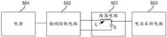
为了对上述电子设备01进行无线充电,如图1所示,电子设备01内设置有无线充电接收电路20和与该无线充电接收电路20连接的电池50。示例的,电子设备01,如图2所示,主要包括显示屏(display panel,DP)10。该显示屏10可以为液晶显示(liquid crystaldisplay,LCD)屏,或者,有机发光二极管(organic light emitting diode,OLED)显示屏。本申请对此不作限定。上述电子设备01还包括如图2所示的中框11和壳体12。显示屏10和壳体12分别位于中框11的两侧,显示屏10的背面朝向壳体12,且该显示屏10和壳体12通过中框11相连接。上述无线充电接收电路20,以及电池50可以设置于中框11朝向壳体12的一侧表面。In order to wirelessly charge the
充电器02包括如图1所示的设置于充电器02内的无线充电电路30,以及与该无线充电电路30连接的电源40。该电源40用于提供充电电能。在本申请的一些实施例中,上述电源40可以为电源适配器。该电源40能够将220V的交流电根据充电功率的需要,转换成直流电(例如5V或10V等),并将该直流电传输至无线充电电路30。The
当将电子设备01的壳体12所在的一侧放在上述充电器02上时,为了对电子设备01进行无线充电,如图3所示,无线充电电路30包括电压转换器301、TX振荡电路302,电压转换器301可以是直流(direct current,DC)转交流(alternating current,AC)转换器,即DC/AC。无线充电接收电路20还包括RX振荡电路201以及整流电路202。When the side where the
基于此,电压转换器301与电源40连接,能够将电源40输出的直流电转换成交流电。此外,TX振荡电路302与电压转换器301连接。TX振荡电路302接收到电压转换器301输出的交流电后,可以产生交变磁场。RX振荡电路201接收上述交变磁场并输出交流电,从而使得TX振荡电路301的功率能够传输至RX振荡电路201。Based on this, the
此外,RX振荡电路201与整流电路202连接,整流电路202可以将整流电路202输出的交流电进行整流,生成整流电压Vrect。在此基础上,上述无线充电接收装置20还包括与整流电路202连接的至少一级电压转换电路203。该电压转换电路203可以将整流电压Vrect转换成电池20的充电电压(例如,3.7V)。该充电电压施加至电池50的两端后,电压转换电路203输出的电流可以对该电池50进行充电。In addition, the
在本申请的一些实施例中,上述电压转换电路203包括DC/DC转换电路。上述DC/DC转换电路可以为降压(Buck)电路或者为开关电容(switched capacitor,SC)电路。其中,Buck电路的输入输出电压比值可以灵活调整,例如输入输出电压比值可以设定为小数。SC电路的输入输出电压比值为整数,但是SC电路可以承受较高的输入输出压差,且具有较高的电压转换效率。如图4所示,提供了一种无线充电电路30的示意图,其中电压转换器301包括开关晶体管Q1-Q4、其中Q1与Q2串联形成第一电桥与电源(电源输出电压Us)并联,Q3与Q4串联形成第二电桥与电源并联;其中,TX振荡电路302包括如图4所示的串联的TX谐振电容CTX以及电感311(电感线圈),其中,TX谐振电容CTX以及电感311串联于第一电桥的中间节点n1与第二电桥的中间节点n2之间。因此,电压转换器301将电源40输出的直流电转换成交流电,并传输至TX振荡电路303后,可以使得电感线圈上产生高频交流电。In some embodiments of the present application, the above-mentioned
此外,为了控制上述充电过程,无线充电电路30和无线充电接收电路20之间可以建立无线通信,在此情况下,如图3所示,无线充电电路30可以包括发送端(transmit,TX)通讯电路303,无线充电接收电路20可以包括接收端(receive,RX)通讯电路204。上述TX通讯电路303和RX通讯电路204之间可以通过蓝牙(bluetooth)、无线宽带(wireless-fidelity,WiFi)、紫蜂协议(Zigbee)、射频识别技术(radio frequency identification,RFID)、远程(long range,Lora)无线技术和近距离无线通信技术(near field communication,NFC)实现无线连接,以使得无线充电电路30和无线充电接收电路20之间可以建立无线通信。这样一来,TX通讯电路303和RX通讯电路204之间可以传输控制信号或者传输充电数据。其中,该充电数据可以用于指示充电类型。示例的,该充电数据可以为充电协议,例如无线充电联盟(wireless power consortium,WPC)推出的无线充电标准Qi,例如BPP(basic powerprofile)协议,或者EPP(extended power profile)协议等。In addition, in order to control the above charging process, wireless communication may be established between the
此外,如图3所示,无线充电电路20还包括与RX通讯电路204连接的RX控制器205。该RX控制器205可以对TX控制器304通过TX通讯电路303发送至RX通讯电路204的充电协议进行识别,以判断出电子设备01的充电类型,例如该充电类型可以为第一充电类型(例如,适用于慢充的小功率充电)或者,上述充电类型可以为第二充电类型(例如,适用于快充的大功率充电)。In addition, as shown in FIG. 3 , the
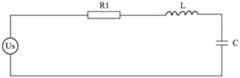
此外,为了实现异物检测,本申请的实施例提供了基于振荡电路的品质因子检测电路。其中该振荡电路可以为上述充电器中无线充电电路的TX振荡电路或者手机中的RX振荡电路。参照图5a、图5b所示,本申请的实施例提供的基于振荡电路的品质因子检测电路包括:振荡电路501、检测控制电路502、以及电压采样电路503。In addition, in order to realize foreign object detection, embodiments of the present application provide a quality factor detection circuit based on an oscillation circuit. The oscillation circuit may be the TX oscillation circuit of the wireless charging circuit in the above-mentioned charger or the RX oscillation circuit of the mobile phone. Referring to FIG. 5 a and FIG. 5 b , the quality factor detection circuit based on an oscillation circuit provided by an embodiment of the present application includes an
其中,检测控制电路502连接电源504,检测控制电路502连接振荡电路501,振荡电路501包括串联的电感L和电容C,其中电感L的第一端连接检测控制电路502,电感L的第二端连接电容C的第一端,电容C的第二端连接公共电压端(例如电源504的负极,如图5b所示)或连接检测控制电路502(如图5a所示);检测控制电路502,用于将电感L和电容C与电源504串联形成充电回路,为电容C充电;检测控制电路502还用于将电感L和电容C连接成LC振荡回路;或者,检测控制电路502用于将电感L和电容C连接成LC振荡回路,并在LC振荡回路上串联预定电阻;电压采样电路503连接电容C的第一端,用于在电感L和电容C形成的LC振荡回路中对电容C的电压采样获取第一峰值电压,在电感L、电容C以及预定电阻形成的LC振荡回路中对电容C的电压采样获取第二峰值电压,其中第一峰值电压以及第二峰值电压用于计算电感L的品质因子Q值。The
其中图5a和图5b的区别是电容C的第二端直接与检测控制电路502连接,或者当检测电路502与振荡电路501连接有相同的公共电压端时,该电容C的第二端也可以直接连接公共电压端。The difference between Fig. 5a and Fig. 5b is that the second end of the capacitor C is directly connected to the
参照图6所示,提供一种基于振荡电路的品质因子检测方法,用于图5示出的基于振荡电路的品质因子检测电路,具体包括如下步骤:Referring to FIG. 6, a quality factor detection method based on an oscillator circuit is provided for the quality factor detection circuit based on an oscillator circuit shown in FIG. 5, which specifically includes the following steps:
601、控制检测控制电路将电感和电容与电源串联形成充电回路,为电容充电。601. The control and detection control circuit connects the inductor and the capacitor in series with the power supply to form a charging loop to charge the capacitor.
602、控制检测控制电路将电感和所述电容连接成LC振荡回路,通过电压采样电路对所述电容进行电压采样,获取电容的第一峰值电压U1。602. Control the detection control circuit to connect the inductor and the capacitor to form an LC oscillation loop, and perform voltage sampling on the capacitor through a voltage sampling circuit to obtain a first peak voltage U1 of the capacitor.
603、控制检测控制电路将电感和电容连接成LC振荡回路,并在LC振荡回路上串联预定电阻,通过电压采样电路对电容进行电压采样,获取电容的第二峰值电压U2。603. Control the detection control circuit to connect the inductor and the capacitor to form an LC oscillating loop, connect a predetermined resistance in series with the LC oscillating loop, and use the voltage sampling circuit to sample the voltage of the capacitor to obtain the second peak voltage U2 of the capacitor.
可以理解的是,步骤602或603在步骤601之后是选择性进行的,即在执行完步骤601之后执行步骤602,或者在执行完601之后执行步骤603,如此在第一次对电容的充电后,执行步骤602,在第二次对电容充电后执行步骤603,当然在第一次对电容的充电后,执行步骤603,或者在第二次对电容充电后执行步骤602也是可以的。It can be understood that
604、通过第一峰值电压和第二峰值电压计算电感的Q值。604. Calculate the Q value of the inductor according to the first peak voltage and the second peak voltage.
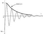
在一种示例中,第一峰值电压为电感和电容连接成的LC振荡回路在电容的第一端生成的阻尼振荡电压中的任意峰值电压,第二峰值电压为预定电阻、电感和电容连接成的LC振荡回路在电容的第一端生成的阻尼振荡电压的任意峰值电压,其中第一峰值电压与第二峰值电压对应阻尼振荡电压中相同周期的峰值电压。例如第一峰值电压在其对应阻尼振荡电压中为第一周期的峰值电压,第二峰值电压在其对应阻尼振荡电压中也为第一周期的峰值电压。当然第一峰值电压以及第二峰值电压也可以采用第二周期或者第N周期的峰值电压。由于当峰值电压越高时测量结果越准确,因此为了提高检测准确性一种优选方案是:第一峰值电压为电感和电容连接成的LC振荡回路在电容的第一端生成的阻尼振荡电压的最大正向峰值电压;第二峰值电压为预定电阻、电感和电容连接成的LC振荡回路在电容的第一端生成的阻尼振荡电压的最大正向峰值电压。In an example, the first peak voltage is any peak voltage in the damped oscillation voltage generated by the LC tank formed by the inductor and the capacitor connected at the first end of the capacitor, and the second peak voltage is a predetermined resistance, the inductor and the capacitor connected to form an arbitrary peak voltage. The LC tank generates any peak voltage of the damped oscillation voltage at the first end of the capacitor, wherein the first peak voltage and the second peak voltage correspond to peak voltages of the same period in the damped oscillation voltage. For example, the first peak voltage is the peak voltage of the first cycle in its corresponding damped oscillation voltage, and the second peak voltage is also the peak voltage of the first cycle in its corresponding damped oscillation voltage. Of course, the first peak voltage and the second peak voltage may also adopt the peak voltage of the second cycle or the Nth cycle. Since the measurement result is more accurate when the peak voltage is higher, in order to improve the detection accuracy, a preferred solution is: the first peak voltage is the sum of the damped oscillation voltage generated at the first end of the capacitor by the LC tank connected by the inductor and the capacitor. The maximum forward peak voltage; the second peak voltage is the maximum forward peak voltage of the damping oscillation voltage generated at the first end of the capacitor by the LC tank formed by the connection of the predetermined resistance, the inductor and the capacitor.
本申请中,步骤604具体可以采用如下公式一计算电感L的等效电感值L1,采用如下公式二计算电感L的等效阻抗R1:In this application,


根据等效电感值L1和等效阻抗R1计算电感的Q值,其中,L1为电感L的等效电感值,R1为电感L的等效阻抗,Us为电源的输出电压(同时Us也为电容C充满的电压值),U1为第一采样电压,U2为第二采样电压,R为预定电阻的阻值,n为正整数,Cp为电容C的容值。其中根据等效电感值L1和等效阻抗R1计算电感的Q值,包括采用如下公式三计算电感L的Q值:Calculate the Q value of the inductor according to the equivalent inductance value L1 and the equivalent impedance R1, where L1 is the equivalent inductance value of the inductor L, R1 is the equivalent impedance of the inductor L, and Us is the output voltage of the power supply (and Us is also the capacitance C full voltage value), U1 is the first sampling voltage, U2 is the second sampling voltage, R is the resistance value of the predetermined resistor, n is a positive integer, and Cp is the capacitance value of the capacitor C. The Q value of the inductance is calculated according to the equivalent inductance value L1 and the equivalent impedance R1, including using the following

在上述方案中,由于检测控制电路502可以将电感L和电容C与电源504串联形成充电回路,为电容C充电;此外检测控制电路502还可以将电感L和电容C连接成LC振荡回路;或者,检测控制电路502用于将电感L和电容C连接成LC振荡回路,并在LC振荡回路上串联预定电阻;如此一来,电源为电容C充电后,电压采样电路可以在电感L和电容C形成的LC振荡回路中对电容C的电压采样获取第一峰值电压;或者在电源为电容C充电后,电压采样电路可以在电感L、电容C以及预定电阻形成的LC振荡回路中对电容C的电压采样获取第二峰值电压;第一峰值电压以及第二峰值电压可以用作电感L的品质因子Q值的计算。可见本申请提供的基于振荡电路的品质因子检测电路,电压的采样过程相对于现有技术无需扫频、并且无需检测LC振荡回路阻尼振荡的频率,因此能够避免扫频或LC振荡回路阻尼振荡的频率对检测时间的限制,此外,能够避免硬件限制导致LC振荡回路阻尼振荡的频率检测难的问题,满足快速高精度的获取Q值。In the above solution, since the
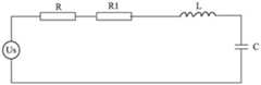
在一种示例中,参照图7a所示,提供一种检测控制电路502的原理性附图,该检测控制电路502包括第一开关组件K1、第二开关组件K2以及预定电阻R;第一开关组件K1的第一端(1)连接电源504(如图7a所示,可以是电源504的正极(+)),第一开关组件K1的第二端(2)连接电容C的第二端,也可以是公共电压端(例如,电源的负极),第一开关组件K1的第三端(3)连接预定电阻R的第一端,预定电阻R的第二端连接电感L的第一端;第二开关组件K2的第一端连接预定电阻R的第一端,第二开关组件K2的第二端连接预定电阻R的第二端。其中,第一开关组件K1的第一端与第一开关组件K1的第三端导通、第二开关组件K2的第一端与第二开关组件K2的第二端导通时,将电感L和电容C与电源504串联形成充电回路,为电容C充电;此外,如图7a所示,为了避免充电电路振荡,电源504的正极与第一开关组件K1的第一端之间串接充电电阻R0。第一开关组件K1的第二端与第一开关组件K1的第三端导通、第二开关组件K2的第一端与第二开关组件K2的第二端导通时,将电感L和电容C连接成LC振荡回路;第一开关组件K1的第二端与第一开关组件K1的第三端导通、第二开关组件K2的第一端与第二开关组件K2的第二端断开时,将电感L和电容C连接成LC振荡回路,并在LC振荡回路上串联预定电阻R。其中,第一开关组件K1包括单刀双掷型继电器或者由至少两个开关器件连接形成,例如由两个开关晶体管连接形成;第二开关组件K2包括开关晶体管或者继电器。其中前述的开关器件或开关晶体管可以采用金属氧化物半导体场效应晶体管(metal-oxide-semiconductor field-effect transistor,MOSFET)。In an example, referring to FIG. 7a, a schematic diagram of a
在一种示例中,参照图7b所示,与图7a不同的是,在该示例中,预定电阻R可以连接在其他位置。其中,该检测控制电路502包括第一开关组件K1、第二开关组件K2以及预定电阻R;第一开关组件K1的第一端(1)连接电源504(如图7b所示,可以是电源504的正极(+)),第一开关组件K1的第二端(2)连接预定电阻R的第一端,预定电阻R的第二端连接电容C的第二端,也可以是公共电压端(例如,电源的负极)或者检测控制电路,第一开关组件K1的第三端(3)连接电感L的第一端;第二开关组件K2的第一端连接预定电阻R的第一端,第二开关组件K2的第二端连接预定电阻R的第二端。其中,第一开关组件K1的第一端与第一开关组件K1的第三端导通时,将电感L和电容C与电源504串联形成充电回路,为电容C充电;此外,如图7b所示,为了避免充电电路振荡,电源504的正极与第一开关组件K1的第一端之间串接充电电阻R0。第一开关组件K1的第二端与第一开关组件K1的第三端导通、第二开关组件K2的第一端与第二开关组件K2的第二端导通时,将电感L和电容C连接成LC振荡回路;第一开关组件K1的第二端与第一开关组件K1的第三端导通、第二开关组件K2的第一端与第二开关组件K2的第二端断开时,将电感L和电容C连接成LC振荡回路,并在LC振荡回路上串联预定电阻R。In an example, as shown in FIG. 7b, different from FIG. 7a, in this example, the predetermined resistance R may be connected in other positions. The
本申请的实施例提供一种基于振荡电路的品质因子检测方法,用于图7a示出的基于振荡电路的品质因子检测电路,具体包括如下步骤:An embodiment of the present application provides a quality factor detection method based on an oscillation circuit, which is used in the quality factor detection circuit based on an oscillation circuit shown in FIG. 7a, and specifically includes the following steps:
701、控制第一开关组件K1的第一端与第一开关组件K1的第三端导通、第二开关组件K2的第一端与第二开关组件K2的第二端导通;将电感L和电容C与电源504串联形成充电回路,为电容C充电。701. Control the first end of the first switch component K1 and the third end of the first switch component K1 to conduct, and the first end of the second switch component K2 and the second end of the second switch component K2 to conduct; connect the inductor L The capacitor C is connected in series with the
其中,当第一开关组件K1的第一端与第一开关组件K1的第三端导通、第二开关组件K2的第一端与第二开关组件K2的第二端导通时,电源与第一开关组件配合形成阶跃信号,向振荡电路输入电压信号Us。Wherein, when the first end of the first switch component K1 is connected to the third end of the first switch component K1 and the first end of the second switch component K2 is connected to the second end of the second switch component K2, the power supply and the second end of the second switch component K2 are connected. The first switch component cooperates to form a step signal, and inputs the voltage signal Us to the oscillating circuit.
702、控制第一开关组件K1的第二端与第一开关组件K1的第三端导通、第二开关组件K2的第一端与第二开关组件K2的第二端导通;通过电压采样电路503对电容进行电压采样,获取电容的第一峰值电压U1。702. Control the conduction between the second end of the first switch component K1 and the third end of the first switch component K1, and control the conduction between the first end of the second switch component K2 and the second end of the second switch component K2; through voltage sampling The
在步骤701中,电源对电容C完成充电,该步骤中,第一开关组件K1的第二端与第一开关组件K1的第三端导通时将电源断开停止对电容C充电,将电感和电容连接成LC振荡回路,且LC振荡回路上仅连接有电感和电容,由于701步骤中对电容C进行了充电,LC振荡回路的电压会产生阻尼振荡,其中电容C放电时,电容C的第一端的电压Uc呈阻尼振荡。电压采样电路503对电容进行电压采样,获取电容的第一峰值电压,示例性的该第一峰值电压,如图8所示,给出了电容第一端的阻尼振荡电压Uc,第一峰值电压可以为最大正向峰值电压U1。需要说明的是第一峰值电压可以为电感和电容连接成的LC振荡回路在电容的第一端生成的阻尼振荡电压中的任意峰值电压。检测控制电路502可以将电感L和电容C与电源504串联形成充电回路,其等效电路如图9所示,由阻尼振荡原理可知,Us(-Us)之后第x个峰值的表达式为:

703、控制第一开关组件K1的第一端与第一开关组件K1的第三端导通、第二开关组件K2的第一端与第二开关组件的第二端导通;将电感L和电容C与电源504串联形成充电回路,为电容C充电。703. Control the first end of the first switch component K1 to conduct with the third end of the first switch component K1, and the first end of the second switch component K2 to conduct the second end of the second switch component; connect the inductance L to the second end of the second switch component. The capacitor C is connected in series with the
704、控制第一开关组件K1的第二端与第一开关组件K1的第三端导通、第二开关组件K2的第一端与第二开关组件K2的第二端断开;通过电压采样电路503对电容进行电压采样,获取电容的第二峰值电压U2。704. Control the second end of the first switch component K1 to be turned on with the third end of the first switch component K1, and the first end of the second switch component K2 to be disconnected from the second end of the second switch component K2; through voltage sampling The
在步骤703中,电源对电容C完成充电,该步骤中,第一开关组件K1的第二端与第一开关组件K1的第三端导通时将电源断开停止对电容C充电,将预定电阻、电感和电容连接成LC振荡回路,且LC振荡回路上连接有预定电阻、电感和电容,由于703步骤中对电容C进行了充电,LC振荡回路的电压会产生阻尼振荡,其中电容C放电时,电容C的第一端的电压Uc呈阻尼振荡。电压采样电路503对电容进行电压采样,获取电容的第二峰值电压U2,示例性的该第二峰值电压U2可以为最大正向峰值电压U2。由于串联了LC振荡回路中串联了预定电阻,此时电容第一端的阻尼振荡电压幅值会相对图8减小。第二峰值电压可以为预定电阻、电感和电容连接成的LC振荡回路在电容的第一端生成的阻尼振荡电压的任意峰值电压。而检测控制电路502可以控制将电感和电容连接成LC振荡回路,并在LC振荡回路上串联预定电阻,其等效电路如图10所示,由阻尼振荡原理可知,Us(-Us)之后第x个峰值的表达式为:

则在步骤702和步骤703中,第一峰值电压U1与第二峰值电压U2对应阻尼振荡电压中相同周期的峰值电压即可。因此参照图11所示,例如第一峰值电压U1可以为在其对应阻尼振荡电压中Us之后的第一个峰值电压,如图11中的第一周期的峰值电压U11,当然第一峰值电压U1也可以采用第二周期或者第N周期的峰值电压U1n。类似的,第二峰值电压U2为与第一峰值电压U1同周期的峰值电压即可。其中,上述公式一、公式二中n取1时,U1的取值为U11,U2的取值为U21。Then, in steps 702 and 703, the first peak voltage U1 and the second peak voltage U2 may correspond to peak voltages of the same period in the damped oscillation voltage. Therefore, referring to FIG. 11 , for example, the first peak voltage U1 may be the first peak voltage after the corresponding damped oscillation voltage Us, such as the peak voltage U11 of the first cycle in FIG. 11 , of course, the first peak voltage U1 can also use the peak voltage U1n of the second cycle or the Nth cycle. Similarly, the second peak voltage U2 may be a peak voltage having the same cycle as the first peak voltage U1. Wherein, when n in the
705、通过第一峰值电压和第二峰值电压计算电感的Q值。705. Calculate the Q value of the inductor according to the first peak voltage and the second peak voltage.
该步骤的具体方式可以参照上述示例此处不再赘述。For the specific manner of this step, reference may be made to the above example and will not be repeated here.
本申请的实施例提供一种基于振荡电路的品质因子检测方法,用于图7b示出的基于振荡电路的品质因子检测电路,具体包括如下步骤:An embodiment of the present application provides a quality factor detection method based on an oscillation circuit, which is used in the quality factor detection circuit based on an oscillation circuit shown in FIG. 7b, and specifically includes the following steps:
801、控制第一开关组件K1的第一端与第一开关组件K1的第三端导通;将电感L和电容C与电源504串联形成充电回路,为电容C充电。801 . Control the first end of the first switch component K1 to conduct with the third end of the first switch component K1 ; connect the inductor L and the capacitor C in series with the
其中,当第一开关组件K1的第一端与第一开关组件K1的第三端导通时,电源与第一开关组件配合形成阶跃信号,向振荡电路输入电压信号Us。Wherein, when the first terminal of the first switch element K1 and the third terminal of the first switch element K1 are turned on, the power supply cooperates with the first switch element to form a step signal, and the voltage signal Us is input to the oscillation circuit.
802、控制第一开关组件K1的第二端与第一开关组件K1的第三端导通、第二开关组件K2的第一端与第二开关组件K2的第二端导通;通过电压采样电路503对电容进行电压采样,获取电容的第一峰值电压U1。802. Control the conduction between the second end of the first switch component K1 and the third end of the first switch component K1, and control the conduction between the first end of the second switch component K2 and the second end of the second switch component K2; through voltage sampling The
该步骤的具体说明可以参考步骤702的描述,不再赘述。For the specific description of this step, reference may be made to the description of step 702, and details are not repeated here.
803、控制第一开关组件K1的第一端与第一开关组件K1的第三端导通,将电感L和电容C与电源504串联形成充电回路,为电容C充电。803 . Control the first end of the first switch component K1 to conduct with the third end of the first switch component K1 , and connect the inductor L and the capacitor C to the
804、控制第一开关组件K1的第二端与第一开关组件K1的第三端导通、第二开关组件K2的第一端与第二开关组件K2的第二端断开;通过电压采样电路503对电容进行电压采样,获取电容的第二峰值电压U2。804. Control the second end of the first switch component K1 to be turned on with the third end of the first switch component K1, and the first end of the second switch component K2 to be disconnected from the second end of the second switch component K2; through voltage sampling The
该步骤的具体说明可以参考步骤704的描述,不再赘述。For the specific description of this step, reference may be made to the description of step 704, and details are not repeated here.
805、通过第一峰值电压和第二峰值电压计算电感的Q值。805. Calculate the Q value of the inductor according to the first peak voltage and the second peak voltage.
该步骤的具体方式可以参照上述示例此处不再赘述。For the specific manner of this step, reference may be made to the above example and will not be repeated here.
在另一种示例中,参照图12所示,检测控制电路502包括第一开关组件M1、第二开关组件M2、第三开关组件M3,以及预定电阻R。In another example, as shown in FIG. 12 , the
第一开关组件R1的第一端连接电源504(例如可以是电源504的正极(+)),第一开关组件M1的第二端连接电感L的第一端;预定电阻R的第一端连接第一开关组件M1的第二端,预定电阻R的第二端连接第二开关组件M2的第一端,第三开关组件M3的第一端连接第一开关组件M1的第二端,第二开关组件M2的第二端以及第三开关组件M3的第二端连接公共电压端连接电容C的第二端,也可以连接公共电压端(例如电源504的负极(-))。The first end of the first switch component R1 is connected to the power supply 504 (for example, the positive pole (+) of the power supply 504), the second end of the first switch component M1 is connected to the first end of the inductor L; the first end of the predetermined resistor R is connected to The second end of the first switch component M1, the second end of the predetermined resistance R is connected to the first end of the second switch component M2, the first end of the third switch component M3 is connected to the second end of the first switch component M1, the second The second terminal of the switch component M2 and the second terminal of the third switch component M3 are connected to the common voltage terminal and the second terminal of the capacitor C, and may also be connected to the common voltage terminal (eg, the negative pole (-) of the power supply 504 ).
其中,第一开关组件M1的第一端与第一开关组件M1的第二端导通、第二开关组件M2的第一端与第二开关组件M2的第二端断开、第三开关组件M3的第一端与第三开关组件M3的第二端断开时,将电感L和电容C与电源504串联形成充电回路,为电容C充电;第一开关组件M1的第一端与第一开关组件M1的第二端断开、第二开关组件M2的第一端与第二开关组件M2的第二端断开、第三开关组件M3的第一端与第三开关组件M3的第二端导通时,将电感L和电容C连接成LC振荡回路;第一开关组件M1的第一端与第一开关组件M1的第二端断开、第二开关组件M2的第一端与第二开关组件M2的第二端导通,第三开关组件M3的第一端与第三开关组件M3的第二端断开时,将电感L和电容C连接成LC振荡回路,并在LC振荡回路的上串联预定电阻R。示例性的,第一开关组件、第二开关组件以及第三开关组件采用继电器或开关晶体管。The first end of the first switch component M1 is connected to the second end of the first switch component M1, the first end of the second switch component M2 is disconnected from the second end of the second switch component M2, and the third switch component When the first end of M3 is disconnected from the second end of the third switch component M3, the inductor L and the capacitor C are connected in series with the
本申请的实施例提供一种基于振荡电路的品质因子检测方法,用于图12示出的基于振荡电路的品质因子检测电路,具体包括如下步骤:An embodiment of the present application provides a quality factor detection method based on an oscillation circuit, which is used in the quality factor detection circuit based on an oscillation circuit shown in FIG. 12 , and specifically includes the following steps:
901、控制第一开关组件M1的第一端与第一开关组件M1的第二端导通、第二开关组件M2的第一端与第二开关组件M2的第二端断开、第三开关组件M3的第一端与第三开关组件M3的第二端断开;将电感和电容与电源串联形成充电回路,为电容C充电。901. Control the first end of the first switch component M1 to be turned on with the second end of the first switch component M1, the first end of the second switch component M2 to be disconnected from the second end of the second switch component M2, and the third switch The first end of the component M3 is disconnected from the second end of the third switch component M3; the inductor and the capacitor are connected in series with the power supply to form a charging loop to charge the capacitor C.
902、控制第一开关组件M1的第一端与第一开关组件M1的第二端断开、第二开关组件M2的第一端与第二开关组件的第二端断开或导通、第三开关组件M3的第一端与第三开关组件的第二端导通;通过电压采样电路对电容进行电压采样,获取电容的第一峰值电压。902. Control the first end of the first switch assembly M1 to be disconnected from the second end of the first switch assembly M1, the first end of the second switch assembly M2 to be disconnected or turned on from the second end of the second switch assembly, and the first end of the second switch assembly M2 to be disconnected or turned on. The first terminal of the three-switch component M3 is connected to the second terminal of the third switch component; the voltage of the capacitor is sampled by the voltage sampling circuit to obtain the first peak voltage of the capacitor.
903、控制第一开关组件M1的第一端与第一开关组件M1的第二端导通、第二开关组件M2的第一端与第二开关组件M2的第二端断开、第三开关组件M3的第一端与第三开关组件M3的第二端断开;将电感和电容与电源串联形成充电回路,为电容充电。903. Control the first end of the first switch component M1 to be turned on with the second end of the first switch component M1, the first end of the second switch component M2 to be disconnected from the second end of the second switch component M2, and the third switch The first end of the component M3 is disconnected from the second end of the third switch component M3; the inductor and the capacitor are connected in series with the power supply to form a charging loop to charge the capacitor.
904、控制第一开关组件M1的第一端与第一开关组件M1的第二端断开、第二开关组件M2的第一端与第二开关组件M2的第二端导通,第三开关组件M3的第一端与第三开关组件M3的第二端断开;通过电压采样电路对电容进行电压采样,获取电容的第二峰值电压。904. Control the first end of the first switch component M1 to be disconnected from the second end of the first switch component M1, the first end of the second switch component M2 to be connected to the second end of the second switch component M2, and the third switch The first end of the component M3 is disconnected from the second end of the third switch component M3; the voltage of the capacitor is sampled by the voltage sampling circuit to obtain the second peak voltage of the capacitor.
905、通过所述第一峰值电压和所述第二峰值电压计算电感的Q值。905. Calculate the Q value of the inductor according to the first peak voltage and the second peak voltage.
其中步骤901-905的具体原理与步骤701-705类似,具体参照上述描述,此处不再赘述。The specific principles of steps 901 to 905 are similar to those of steps 701 to 705, and specific reference is made to the above description, which will not be repeated here.
此外,检测控制电路502,还包括第四开关组件M4;第四开关组件M4的第一端连接电容C的第二端,第四开关组件M4的第二端连接公共电压端或连接检测控制电路502。当然在检测控制电路502包含第四开关组件M4时,在上述步骤901-904中,需要控制M4均为导通状态。In addition, the
需要说明的是,为了节省电路成本,当该图12所示的基于振荡电路的品质因子检测电路用于充电器中时,第三开关组件M3可以复用图4中的第一电桥中的下桥臂的开关晶体管Q2;此外,第四开关组件M4可以复用图4中的第二电桥中的下桥臂的开关晶体管Q4连接电源的负极(-)。即如图13所示,直接在图4的基础上增加了M1、M2、R0、R,其中M1、M2、R0、R的连接关系参照图12中的具体描述,这里不再赘述。当然在基于振荡电路的品质因子检测电路包含开关晶体管Q4时,在上述步骤901-904中,需要控制Q4均为导通状态。此外需要说明的是,本申请的实施例提供基于振荡电路的品质因子检测电路可以与图4提供的无线充电电路同源或不同源,如图13所示,在两者不同源时,基于振荡电路的品质因子检测电路采用电压源Us,无线充电电路采用电压源Udc。It should be noted that, in order to save the circuit cost, when the quality factor detection circuit based on the oscillator circuit shown in FIG. 12 is used in the charger, the third switch component M3 can reuse the The switching transistor Q2 of the lower bridge arm; in addition, the fourth switching component M4 can reuse the switching transistor Q4 of the lower bridge arm in the second bridge in FIG. 4 to connect the negative pole (-) of the power supply. That is, as shown in FIG. 13 , M1, M2, R0, and R are added directly on the basis of FIG. 4, wherein the connection relationship of M1, M2, R0, and R is referred to the specific description in FIG. 12, and will not be repeated here. Of course, when the quality factor detection circuit based on the oscillator circuit includes the switching transistor Q4, in the above steps 901-904, it is necessary to control the Q4 to be in an on state. In addition, it should be noted that the quality factor detection circuit based on the oscillation circuit provided by the embodiments of the present application may be of the same source or different from the wireless charging circuit provided in FIG. 4 , as shown in FIG. The quality factor detection circuit of the circuit adopts the voltage source Us, and the wireless charging circuit adopts the voltage source Udc.
此外,电压采样电路包括以下任意一种:电压跟随电路、峰值电压采样电路、逐波峰值电压采样电路、电压衰减检测电路。In addition, the voltage sampling circuit includes any one of the following: a voltage follower circuit, a peak voltage sampling circuit, a wave-by-wave peak voltage sampling circuit, and a voltage decay detection circuit.
如图14所示,提供一种电压采样电路的示意图,电压采样电路为电压跟随电路,该电压跟随电路包括:电压跟随器g1和二极管D1,由于电压跟随器g1的3端和1端电压相等,可以通过在g1的1端连接二极管D1采样电容C的峰值电压。如图15所示,提供另一种电压采样电路的示意图,电压采样电路为峰值电压采样电路,该峰值电压采样电路包括二极管D2和C1,由二极管D2的单向导通作用以及C1的储能作用,随着电容C的第一端上输出的阻尼振荡电压,C1上的电压值保持在峰值电压。如图16所示,提供了电容C的第一端上的阻尼振荡电压的曲线,以及C1的电压,可以看出C1上的电压保持稳定为峰值电压U1。当电压采样电路采用逐波峰值电压采样电路时,如图17所示,该逐波峰值电压采样电路用于逐次采集阻尼振荡电压的每个周期的波峰,因此U1也可为逐波峰值电压采样电路采集的阻尼振荡电压的曲线的第一个周期峰值电压,或者也可为阻尼振荡电压的曲线的第二甚至第N个周期的峰值电压,与图14的区别是,图17示出的逐波峰值电压采样电路还包括电压跟随器g1的3端的连接有延时开关Ky,其中,延时开关Ky可以选择在不同的延时开启将电容C的第一端与电压跟随器g1的3端连接,从而实现对阻尼振荡电压各个周期的波峰的采集。As shown in FIG. 14, a schematic diagram of a voltage sampling circuit is provided. The voltage sampling circuit is a voltage follower circuit. The voltage follower circuit includes: a voltage follower g1 and a diode D1. Since the voltages of the 3-terminal and the 1-terminal of the voltage follower g1 are equal , the peak voltage of capacitor C can be sampled by connecting diode D1 to 1 terminal of g1. As shown in FIG. 15 , a schematic diagram of another voltage sampling circuit is provided. The voltage sampling circuit is a peak voltage sampling circuit. The peak voltage sampling circuit includes diodes D2 and C1. The unidirectional conduction of the diode D2 and the energy storage function of C1 , with the damped oscillation voltage output on the first end of capacitor C, the voltage value on C1 remains at the peak voltage. As shown in FIG. 16 , a curve of the damped oscillation voltage on the first terminal of capacitor C is provided, and the voltage of C1 , and it can be seen that the voltage on C1 remains stable at the peak voltage U1 . When the voltage sampling circuit adopts the wave-by-wave peak voltage sampling circuit, as shown in Figure 17, the wave-by-wave peak voltage sampling circuit is used to successively collect the peaks of each cycle of the damped oscillation voltage, so U1 can also be the wave-by-wave peak voltage sampling circuit. The peak voltage of the first cycle of the curve of the damped oscillation voltage collected by the circuit, or it can also be the peak voltage of the second or even the Nth cycle of the curve of the damped oscillation voltage. The wave peak voltage sampling circuit also includes a delay switch Ky connected to the third terminal of the voltage follower g1, wherein the delay switch Ky can be selected to be turned on at different delays to connect the first terminal of the capacitor C and the third terminal of the voltage follower g1. connection, so as to realize the acquisition of the peaks of each cycle of the damped oscillation voltage.
如图18所示,提供又一种电压采样电路的示意图,电压采样电路为电压衰减检测电路,该电压衰减检测电路包括:电压跟随器g1、电阻R2-R6、二极管D1以及电容C2、C3;其中电压跟随器g1的4端连接电源V11的负极(-),5端连接电源V11的正极(+),3端通过电阻R2连接电容C的第一端,1端连接二极管D1的阳极,二极管D1的阴极通过电阻R3连接电压跟随器g1的2端,二极管D1的阴极还连接电阻R4的第一端,R4的第二端通过电容C2连接电源V11的负极(-),R4的第二端通过电阻R6连接电源V11的负极(-),R4的第二端连接电阻R5的第一端,R5的第二端通过电容C3连接电源V11的负极(-),其中通过R5的第二端(Vo)可以采样电容C3的电压,电容C3的电压为电容C的阻尼振荡电压的衰减曲线,如图19所示,可以看出C3上的最大电压为峰值电压U1。当然上述图14、图16、图17中示出的电压采样电路仅包含了解释电路原理的必要部件,在一些方案中,还可能有其他外围元器件。此外,图14、图15、图17、图18中除电压采样电路部分之外的电路均是采用图7中的原理性示意图中的电路为例进行说明;当作为一种实施例时,图14、图15、图17、图18除电压采样电路部分之外的电路也可以替换为图12或图13示出的电路。As shown in FIG. 18, a schematic diagram of another voltage sampling circuit is provided. The voltage sampling circuit is a voltage decay detection circuit, and the voltage decay detection circuit includes: a voltage follower g1, resistors R2-R6, diode D1, and capacitors C2 and C3; The 4th terminal of the voltage follower g1 is connected to the negative pole (-) of the power supply V11, the 5th terminal is connected to the positive pole (+) of the power supply V11, the 3rd terminal is connected to the first terminal of the capacitor C through the resistor R2, and the 1st terminal is connected to the anode of the diode D1. The cathode of D1 is connected to the two terminals of the voltage follower g1 through the resistor R3, the cathode of the diode D1 is also connected to the first terminal of the resistor R4, the second terminal of R4 is connected to the negative terminal (-) of the power supply V11 through the capacitor C2, and the second terminal of R4 Connect the negative electrode (-) of the power supply V11 through the resistor R6, the second end of the R4 is connected to the first end of the resistor R5, the second end of the R5 is connected to the negative electrode (-) of the power supply V11 through the capacitor C3, and the second end of the R5 ( Vo) can sample the voltage of capacitor C3. The voltage of capacitor C3 is the attenuation curve of the damped oscillation voltage of capacitor C. As shown in Figure 19, it can be seen that the maximum voltage on C3 is the peak voltage U1. Of course, the voltage sampling circuits shown in Fig. 14, Fig. 16, and Fig. 17 only include necessary components to explain the circuit principle. In some solutions, there may also be other peripheral components. In addition, the circuits in FIGS. 14 , 15 , 17 , and 18 except for the voltage sampling circuit part are all described by using the circuit in the schematic diagram in FIG. 7 as an example; when used as an embodiment, FIG. 14, Fig. 15, Fig. 17, Fig. 18 The circuits other than the voltage sampling circuit part can also be replaced with the circuits shown in Fig. 12 or Fig. 13.
可以理解的是,以上各个实施例提供的基于振荡电路的品质因子检测方法,可以由基于振荡电路的品质因子检测装置实现,上述的方法和/或步骤,也可以由可用于基于振荡电路的品质因子检测装置的部件(例如芯片或者电路)实现。It can be understood that the quality factor detection methods based on oscillator circuits provided in the above embodiments can be implemented by a quality factor detection device based on oscillator circuits, and the above methods and/or steps can also be used for oscillator circuit-based quality factors. A component (eg, a chip or circuit) of a factor detection device is implemented.
可以理解的是,该基于振荡电路的品质因子检测装置为了实现上述功能,其包含了执行各个功能相应的硬件结构和/或软件模块。本领域技术人员应该很容易意识到,结合本文中所公开的实施例描述的各示例的单元及算法步骤,本申请能够以硬件或硬件和计算机软件的结合形式来实现。某个功能究竟以硬件还是计算机软件驱动硬件的方式来执行,取决于技术方案的特定应用和设计约束条件。专业技术人员可以对每个特定的应用来使用不同方法来实现所描述的功能,但是这种实现不应认为超出本申请的范围。It can be understood that, in order to realize the above-mentioned functions, the device for detecting quality factor based on an oscillator circuit includes corresponding hardware structures and/or software modules for executing each function. Those skilled in the art should easily realize that the present application can be implemented in hardware or a combination of hardware and computer software with the units and algorithm steps of each example described in conjunction with the embodiments disclosed herein. Whether a function is performed by hardware or computer software driving hardware depends on the specific application and design constraints of the technical solution. Skilled artisans may implement the described functionality using different methods for each particular application, but such implementations should not be considered beyond the scope of this application.
本申请实施例可以根据上述方法实施例中对基于振荡电路的品质因子检测装置进行功能模块的划分,例如,可以对应各个功能划分各个功能模块,也可以将两个或两个以上的功能集成在一个处理模块中。上述集成的模块既可以采用硬件的形式实现,也可以采用软件功能模块的形式实现。需要说明的是,本申请实施例中对模块的划分是示意性的,仅仅为一种逻辑功能划分,实际实现时可以有另外的划分方式。In this embodiment of the present application, functional modules may be divided into the quality factor detection apparatus based on the oscillator circuit according to the above method embodiments. For example, each functional module may be divided into each function, or two or more functions may be integrated in in a processing module. The above-mentioned integrated modules can be implemented in the form of hardware, and can also be implemented in the form of software function modules. It should be noted that, the division of modules in the embodiments of the present application is schematic, and is only a logical function division, and there may be other division manners in actual implementation.
图20示出了一种基于振荡电路的品质因子检测装置的结构示意图。该基于振荡电路的品质因子检测装置包括控制模块2001、处理模块2002。FIG. 20 shows a schematic structural diagram of a quality factor detection device based on an oscillator circuit. The device for detecting quality factor based on an oscillator circuit includes a control module 2001 and a processing module 2002 .
控制模块2001,用于控制所述检测控制电路将所述电感和电容与所述电源串联形成充电回路,为所述电容充电;A control module 2001, configured to control the detection control circuit to connect the inductor and the capacitor in series with the power supply to form a charging loop to charge the capacitor;
所述控制模块2001,还用于控制所述检测控制电路将所述电感和所述电容连接成LC振荡回路,通过所述电压采样电路对所述电容进行电压采样,获取所述电容的第一峰值电压;或者,控制所述检测控制电路将所述电感和所述电容连接成LC振荡回路,并在所述LC振荡回路上串联预定电阻,通过所述电压采样电路对所述电容进行电压采样,获取所述电容的第二峰值电压;The control module 2001 is further configured to control the detection control circuit to connect the inductor and the capacitor into an LC oscillating circuit, perform voltage sampling on the capacitor through the voltage sampling circuit, and obtain the first value of the capacitor. peak voltage; or, control the detection control circuit to connect the inductor and the capacitor to form an LC oscillating circuit, and connect a predetermined resistor in series with the LC oscillating circuit, and perform voltage sampling on the capacitor through the voltage sampling circuit , obtain the second peak voltage of the capacitor;
处理模块2002,用于通过所述电压采样电路获取的第一峰值电压和所述第二峰值电压计算所述电感的Q值。The processing module 2002 is configured to calculate the Q value of the inductance through the first peak voltage and the second peak voltage obtained by the voltage sampling circuit.
可选的,检测控制电路包括第一开关组件、第二开关组件以及所述预定电阻;所述第一开关组件的第一端连接所述电源,所述第一开关组件的第二端连接所述公共电压端或连接所述电容的第二端,所述第一开关组件的第三端连接所述预定电阻的第一端,所述预定电阻的第二端连接所述电感的第一端;所述第二开关组件的第一端连接所述预定电阻的第一端,所述第二开关组件的第二端连接所述预定电阻的第二端;所述控制模块2001具体用于控制所述第一开关组件的第一端与所述第一开关组件的第三端导通、所述第二开关组件的第一端与所述第二开关组件的第二端导通;所述控制模块2001具体用于控制所述第一开关组件的第二端与所述第一开关组件的第三端导通、所述第二开关组件的第一端与所述第二开关组件的第二端导通;所述控制模块具体用于控制所述第一开关组件的第二端与所述第一开关组件的第三端导通、所述第二开关组件的第一端与所述第二开关组件的第二端断开。Optionally, the detection control circuit includes a first switch component, a second switch component, and the predetermined resistance; a first end of the first switch component is connected to the power supply, and a second end of the first switch component is connected to the power supply. the common voltage terminal or the second terminal of the capacitor, the third terminal of the first switch component is connected to the first terminal of the predetermined resistor, and the second terminal of the predetermined resistor is connected to the first terminal of the inductor ; The first end of the second switch component is connected to the first end of the predetermined resistance, and the second end of the second switch component is connected to the second end of the predetermined resistance; the control module 2001 is specifically used to control The first end of the first switch component is connected to the third end of the first switch component, and the first end of the second switch component is connected to the second end of the second switch component; the The control module 2001 is specifically configured to control the conduction between the second end of the first switch assembly and the third end of the first switch assembly, and the first end of the second switch assembly and the third end of the second switch assembly. The two terminals are connected; the control module is specifically configured to control the conduction between the second terminal of the first switch component and the third terminal of the first switch component, and the first terminal of the second switch component to be connected to the third terminal of the first switch component. The second end of the second switch assembly is disconnected.
可选的,所述检测控制电路包括第一开关组件、第二开关组件以及所述预定电阻;所述第一开关组件的第一端连接所述电源,所述第一开关组件的第二端连接所述预定电阻的第一端,所述预定电阻的第二端连接所述公共电压端或连接所述电容的第二端,所述第一开关组件的第三端连接所述电感的第一端;所述第二开关组件的第一端连接所述预定电阻的第一端,所述第二开关组件的第二端连接所述预定电阻的第二端;所述控制模块2001具体用于控制控制所述第一开关组件的第一端与所述第一开关组件的第三端导通;所述控制模块2001具体用于控制所述第一开关组件的第二端与所述第一开关组件的第三端导通、所述第二开关组件的第一端与所述第二开关组件的第二端导通;所述控制模块2001具体用于控制所述第一开关组件的第二端与所述第一开关组件的第三端导通、所述第二开关组件的第一端与所述第二开关组件的第二端断开。Optionally, the detection control circuit includes a first switch component, a second switch component, and the predetermined resistance; a first end of the first switch component is connected to the power supply, and a second end of the first switch component The first terminal of the predetermined resistor is connected, the second terminal of the predetermined resistor is connected to the common voltage terminal or the second terminal of the capacitor is connected, and the third terminal of the first switch component is connected to the first terminal of the inductor. one end; the first end of the second switch component is connected to the first end of the predetermined resistance, and the second end of the second switch component is connected to the second end of the predetermined resistance; the control module 2001 is specifically The control module 2001 is specifically used to control the second end of the first switch assembly and the third end of the first switch assembly to be connected The third end of a switch assembly is turned on, the first end of the second switch assembly is connected to the second end of the second switch assembly; the control module 2001 is specifically used to control the first switch assembly The second end is connected to the third end of the first switch assembly, and the first end of the second switch assembly is disconnected from the second end of the second switch assembly.
可选的,所述检测控制电路包括第一开关组件、第二开关组件、第三开关组件,以及所述预定电阻;所述第一开关组件的第一端连接所述电源,所述第一开关组件的第二端连接所述电感的第一端;所述预定电阻的第一端连接所述第一开关组件的第二端,所述预定电阻的第二端连接所述第二开关组件的第一端;所述第三开关组件的第一端连接所述第一开关组件的第二端,所述第二开关组件的第二端以及所述第三开关组件的第二端连接所述公共电压端或连接所述电容C的第二端;所述控制模块2001具体用于控制所述第一开关组件的第一端与所述第一开关组件的第二端导通、所述第二开关组件的第一端与所述第二开关组件的第二端断开、所述第三开关组件的第一端与所述第三开关组件的第二端断开;所述控制模块2001具体用于控制所述第一开关组件的第一端与所述第一开关组件的第二端断开、所述第二开关组件的第一端与所述第二开关组件的第二端断开或导通、所述第三开关组件的第一端与所述第三开关组件的第二端导通;所述控制模块2001具体用于控制所述第一开关组件的第一端与所述第一开关组件的第二端断开、所述第二开关组件的第一端与所述第二开关组件的第二端导通,所述第三开关组件的第一端与所述第三开关组件的第二端断开。Optionally, the detection control circuit includes a first switch component, a second switch component, a third switch component, and the predetermined resistance; a first end of the first switch component is connected to the power supply, and the first switch component is connected to the power supply. The second end of the switch component is connected to the first end of the inductor; the first end of the predetermined resistance is connected to the second end of the first switch component, and the second end of the predetermined resistance is connected to the second switch component the first end of the third switch assembly; the first end of the third switch assembly is connected to the second end of the first switch assembly, the second end of the second switch assembly and the second end of the third switch assembly are connected to the The common voltage terminal or the second terminal connected to the capacitor C; the control module 2001 is specifically configured to control the first terminal of the first switch component to conduct with the second terminal of the first switch component The first end of the second switch assembly is disconnected from the second end of the second switch assembly, the first end of the third switch assembly is disconnected from the second end of the third switch assembly; the control module 2001 is specifically used to control the disconnection between the first end of the first switch assembly and the second end of the first switch assembly, and the first end of the second switch assembly and the second end of the second switch assembly Disconnected or turned on, the first end of the third switch component is connected to the second end of the third switch component; the control module 2001 is specifically used to control the first end of the first switch component to be connected to The second end of the first switch assembly is disconnected, the first end of the second switch assembly is connected to the second end of the second switch assembly, and the first end of the third switch assembly is connected to the second end of the second switch assembly. The second end of the third switch assembly is disconnected.
可选的,所述检测控制电路还包括第四开关组件;所述第四开关组件的第一端连接所述电容的第二端,所述第四开关组件的第二端连接所述公共电压端或连接所述检测控制电路;所述控制模块2001具体用于控制所述第一开关组件的第一端与所述第一开关组件的第二端导通、所述第二开关组件的第一端与所述第二开关组件的第二端断开、所述第三开关组件的第一端与所述第三开关组件的第二端断开、所述第四开关组件的第一端与所述第四开关组件的第二端导通;所述控制模块2001具体用于控制所述第一开关组件的第一端与所述第一开关组件的第二端断开、所述第二开关组件的第一端与所述第二开关组件的第二端断开或导通、所述第三开关组件的第一端与所述第三开关组件的第二端导通、所述第四开关组件的第一端与所述第四开关组件的第二端导通;所述控制模块2001具体用于控制所述第一开关组件的第一端与所述第一开关组件的第二端断开、所述第二开关组件的第一端与所述第二开关组件的第二端导通,所述第三开关组件的第一端与所述第三开关组件的第二端断开、所述第四开关组件的第一端与所述第四开关组件的第二端导通。Optionally, the detection control circuit further includes a fourth switch component; the first end of the fourth switch component is connected to the second end of the capacitor, and the second end of the fourth switch component is connected to the common voltage terminal or connected to the detection control circuit; the control module 2001 is specifically used to control the conduction between the first terminal of the first switch component and the second terminal of the first switch component, and the first terminal of the second switch component to conduct One end is disconnected from the second end of the second switch assembly, the first end of the third switch assembly is disconnected from the second end of the third switch assembly, and the first end of the fourth switch assembly is connected to the second end of the fourth switch assembly; the control module 2001 is specifically configured to control the first end of the first switch assembly to be disconnected from the second end of the first switch assembly, and the first end of the first switch assembly to be disconnected. The first end of the second switch assembly is disconnected or connected to the second end of the second switch assembly, the first end of the third switch assembly is connected to the second end of the third switch assembly, the The first end of the fourth switch assembly is connected to the second end of the fourth switch assembly; the control module 2001 is specifically used to control the first end of the first switch assembly and the second end of the first switch assembly. The two terminals are disconnected, the first end of the second switch assembly is connected to the second end of the second switch assembly, and the first end of the third switch assembly is connected to the second end of the third switch assembly disconnected, the first end of the fourth switch assembly is connected to the second end of the fourth switch assembly.
可选的,处理模块2002具体用于采用如下公式一计算所述电感的等效电感值,采用如下公式二计算所述电感的等效阻抗:Optionally, the processing module 2002 is specifically configured to use the following


根据所述等效电感值和所述等效阻抗计算所述电感的Q值,其中,L1为所述电感的等效电感值,R1为所述电感的等效阻抗,Us为所述电源的输出电压,U1为所述第一采样电压,U2为所述第二采样电压,R为预定电阻的阻值,Cp为电容的容值。Calculate the Q value of the inductor according to the equivalent inductance value and the equivalent impedance, where L1 is the equivalent inductance value of the inductor, R1 is the equivalent impedance of the inductor, and Us is the power supply Output voltage, U1 is the first sampling voltage, U2 is the second sampling voltage, R is the resistance value of the predetermined resistor, and Cp is the capacitance value of the capacitor.
可选的,处理模块2002具体用于采用如下公式三计算所述电感的Q值:Optionally, the processing module 2002 is specifically configured to calculate the Q value of the inductance by using the following formula 3:

其中,上述方法实施例涉及的各步骤的所有相关内容均可以援引到对应功能模块的功能描述,在此不再赘述。Wherein, all relevant contents of the steps involved in the above method embodiments can be cited in the functional descriptions of the corresponding functional modules, which will not be repeated here.
在本实施例中,该基于振荡电路的品质因子检测装置以采用集成的方式划分各个功能模块的形式来呈现。这里的“模块”可以指特定ASIC,电路,执行一个或多个软件或固件程序的处理器和存储器,集成逻辑电路,和/或其他可以提供上述功能的器件。In this embodiment, the device for detecting quality factor based on an oscillator circuit is presented in the form of dividing each functional module in an integrated manner. "Module" herein may refer to a specific ASIC, circuit, processor and memory executing one or more software or firmware programs, integrated logic circuit, and/or other device that may provide the functions described above.
如图21所示,本申请的实施例提供一种基于振荡电路的品质因子检测装置的硬件结构示意图。As shown in FIG. 21 , an embodiment of the present application provides a schematic diagram of the hardware structure of an apparatus for detecting a quality factor based on an oscillator circuit.
其中,基于振荡电路的品质因子检测装置包括至少一个处理器(图20中示例性的以包括一个处理器2101为例进行说明)和至少一个接口电路2103(图21中示例性的以包括一个接口电路2103为例进行说明)。可选的,基于振荡电路的品质因子检测装置还可以包括至少一个存储器(图21中示例性的以包括一个存储器2102为例进行说明)。Wherein, the quality factor detection device based on the oscillator circuit includes at least one processor (in FIG. 20 , it is exemplified to include a processor 2101 ) and at least one interface circuit 2103 (in FIG. 21 , as an example, includes an interface The
处理器2101、存储器2102和接口电路2103通过通信线路相连接。通信线路可包括一通路,在上述组件之间传送信息。The
处理器2101可以是通用中央处理器(central processing unit,CPU)、微处理器、特定应用集成电路(application-specific integrated circuit,ASIC),或者一个或多个用于控制本申请方案程序执行的集成电路。在具体实现中,作为一种实施例,处理器2101也可以包括多个CPU,并且处理器2101可以是单核(single-CPU)处理器或多核(multi-CPU)处理器。这里的处理器可以指一个或多个设备、电路或用于处理数据(例如计算机程序指令)的处理核。The
存储器2102可以是具有存储功能的装置。例如可以是只读存储器(read-onlymemory,ROM)或可存储静态信息和指令的其他类型的静态存储设备、随机存取存储器(random access memory,RAM)或者可存储信息和指令的其他类型的动态存储设备,也可以是电可擦可编程只读存储器(electrically erasable programmable read-only memory,EEPROM)、只读光盘(compact disc read-only memory,CD-ROM)或其他光盘存储、光碟存储(包括压缩光碟、激光碟、光碟、数字通用光碟、蓝光光碟等)、磁盘存储介质或者其他磁存储设备、或者能够用于携带或存储具有指令或数据结构形式的期望的程序代码并能够由计算机存取的任何其他介质,但不限于此。存储器2102可以是独立存在,通过通信线路与处理器2101相连接。存储器2102也可以和处理器2101集成在一起。The
其中,存储器2102用于存储执行本申请方案的计算机执行指令,并由处理器2101来控制执行。具体的,处理器2101用于执行存储器2102中存储的计算机执行指令,从而实现本申请实施例中所述的基于振荡电路的品质因子检测方法。The
或者,可选的,本申请实施例中,也可以是处理器2101执行本申请下述实施例提供的基于振荡电路的品质因子检测方法中的处理相关的功能,接口电路2103负责与其他部件连接以实现信号的传输,例如对各个开关组件的控制,具体可以是对检测控制电路中开关组件的闭合或断开的控制信号;又例如传输电压采样电路生成的峰值电压,本申请实施例对此不作具体限定。Or, optionally, in this embodiment of the present application, the
可选的,本申请实施例中的计算机执行指令也可以称之为应用程序代码或者计算机程序代码,本申请实施例对此不作具体限定。Optionally, the computer-executed instructions in the embodiment of the present application may also be referred to as application program code or computer program code, which is not specifically limited in the embodiment of the present application.
在具体实现中,作为一种实施例,处理器2101可以包括一个或多个CPU,例如图21中的CPU0和CPU1。In a specific implementation, as an embodiment, the
在具体实现中,作为一种实施例,基于振荡电路的品质因子检测装置可以包括多个处理器,例如图21中的处理器2101和处理器2104。这些处理器中的每一个可以是一个单核(single-CPU)处理器,也可以是一个多核(multi-CPU)处理器。这里的处理器可以指一个或多个设备、电路、和/或用于处理数据(例如计算机程序指令)的处理核。In a specific implementation, as an embodiment, the apparatus for detecting quality factor based on an oscillator circuit may include multiple processors, for example, the
其中,图21所示的基于振荡电路的品质因子检测装置中的处理器2101可以通过调用存储器2102中存储的计算机执行指令,使得基于振荡电路的品质因子检测装置执行上述方法实施例中的方法。具体的,图20中的控制模块2001、处理模块2002的功能/实现过程可以通过图21所示的基于振荡电路的品质因子检测装置中的处理器2101调用存储器2102中存储的计算机执行指令来实现。由于本实施例提供的基于振荡电路的品质因子检测装置可执行上述的方法,因此其所能获得的技术效果可参考上述方法实施例,在此不再赘述。The
可选的,本申请实施例还提供了一种基于振荡电路的品质因子检测装置(例如,该基于振荡电路的品质因子检测装置可以是芯片或芯片系统),该基于振荡电路的品质因子检测装置包括处理器,用于实现上述任一方法实施例中的方法。在一种可能的设计中,该基于振荡电路的品质因子检测装置还包括存储器。该存储器,用于保存必要的程序指令和数据,处理器可以调用存储器中存储的程序代码以指令该基于振荡电路的品质因子检测装置执行上述任一方法实施例中的方法。当然,存储器也可以不在该基于振荡电路的品质因子检测装置中。该基于振荡电路的品质因子检测装置是芯片系统时,可以由芯片构成,也可以包含芯片和其他分立器件,本申请实施例对此不作具体限定。Optionally, the embodiment of the present application further provides a quality factor detection device based on an oscillator circuit (for example, the quality factor detection device based on an oscillator circuit may be a chip or a chip system), the quality factor detection device based on an oscillator circuit A processor is included for implementing the method in any of the above method embodiments. In a possible design, the device for detecting quality factor based on an oscillator circuit further includes a memory. The memory is used to store necessary program instructions and data, and the processor can call the program codes stored in the memory to instruct the oscillator circuit-based quality factor detection apparatus to execute the method in any of the above method embodiments. Of course, the memory may not be included in the quality factor detection device based on the oscillation circuit. When the quality factor detection device based on the oscillation circuit is a chip system, it may be composed of a chip, or may include a chip and other discrete devices, which is not specifically limited in the embodiment of the present application.
此外本申请的实施例提供一种电子设备,包括:上述的基于振荡电路的品质因子检测电路以及基于振荡电路的品质因子检测装置,其中电子设备可以为发射端设备或者接收端设备。In addition, an embodiment of the present application provides an electronic device, including: the above-mentioned oscillator circuit-based quality factor detection circuit and an oscillator circuit-based quality factor detection device, wherein the electronic device may be a transmitter device or a receiver device.
在上述实施例中,可以全部或部分地通过软件、硬件、固件或者其任意组合来实现。当使用软件程序实现时,可以全部或部分地以计算机程序产品的形式来实现。该计算机程序产品包括一个或多个计算机指令。在计算机上加载和执行计算机程序指令时,全部或部分地产生按照本申请实施例所述的流程或功能。所述计算机可以是通用计算机、专用计算机、计算机网络、或者其他可编程装置。所述计算机指令可以存储在计算机可读存储介质中,或者从一个计算机可读存储介质向另一个计算机可读存储介质传输。所述计算机可读存储介质可以是计算机能够存取的任何可用介质或者是包含一个或多个可以用介质集成的服务器、数据中心等数据存储设备。所述可用介质可以是磁性介质(例如,软盘、硬盘、磁带),光介质(例如,DVD)、或者半导体介质(例如固态硬盘(solid state disk,SSD))等。本申请实施例中,计算机可以包括前面所述的装置。In the above-mentioned embodiments, it may be implemented in whole or in part by software, hardware, firmware or any combination thereof. When implemented using a software program, it can be implemented in whole or in part in the form of a computer program product. The computer program product includes one or more computer instructions. When the computer program instructions are loaded and executed on the computer, all or part of the processes or functions described in the embodiments of the present application are generated. The computer may be a general purpose computer, special purpose computer, computer network, or other programmable device. The computer instructions may be stored in or transmitted from one computer-readable storage medium to another computer-readable storage medium. The computer-readable storage medium can be any available medium that can be accessed by a computer or data storage devices including one or more servers, data centers, etc. that can be integrated with the medium. The usable media may be magnetic media (eg, floppy disks, hard disks, magnetic tapes), optical media (eg, DVDs), or semiconductor media (eg, solid state disks (SSDs)), and the like. In this embodiment of the present application, the computer may include the aforementioned apparatus.
尽管在此结合各实施例对本申请进行了描述,然而,在实施所要求保护的本申请过程中,本领域技术人员通过查看所述附图、公开内容、以及所附权利要求书,可理解并实现所述公开实施例的其他变化。在权利要求中,“包括”(comprising)一词不排除其他组成部分或步骤,“一”或“一个”不排除多个的情况。单个处理器或其他单元可以实现权利要求中列举的若干项功能。相互不同的从属权利要求中记载了某些措施,但这并不表示这些措施不能组合起来产生良好的效果。Although the application is described herein in conjunction with the various embodiments, those skilled in the art will understand and understand from a review of the drawings, the disclosure, and the appended claims in practicing the claimed application. Other variations of the disclosed embodiments are implemented. In the claims, the word "comprising" does not exclude other components or steps, and "a" or "an" does not exclude a plurality. A single processor or other unit may fulfill the functions of several items recited in the claims. The mere fact that certain measures are recited in mutually different dependent claims does not indicate that these measures cannot be combined to advantage.
尽管结合具体特征及其实施例对本申请进行了描述,显而易见的,在不脱离本申请的精神和范围的情况下,可对其进行各种修改和组合。相应地,本说明书和附图仅仅是所附权利要求所界定的本申请的示例性说明,且视为已覆盖本申请范围内的任意和所有修改、变化、组合或等同物。显然,本领域的技术人员可以对本申请进行各种改动和变型而不脱离本申请的精神和范围。这样,倘若本申请的这些修改和变型属于本申请权利要求及其等同技术的范围之内,则本申请也意图包含这些改动和变型在内。Although the application has been described in conjunction with specific features and embodiments thereof, it will be apparent that various modifications and combinations can be made therein without departing from the spirit and scope of the application. Accordingly, this specification and drawings are merely exemplary illustrations of the application as defined by the appended claims, and are deemed to cover any and all modifications, variations, combinations or equivalents within the scope of this application. Obviously, those skilled in the art can make various changes and modifications to the present application without departing from the spirit and scope of the present application. Thus, if these modifications and variations of the present application fall within the scope of the claims of the present application and their equivalents, the present application is also intended to include these modifications and variations.
Claims (20)
Translated fromChinese


Priority Applications (1)
| Application Number | Priority Date | Filing Date | Title |
|---|---|---|---|
| CN202210307078.2ACN114878919A (en) | 2020-05-27 | 2020-05-27 | Quality factor detection circuit and method based on oscillation circuit and electronic equipment |
Applications Claiming Priority (2)
| Application Number | Priority Date | Filing Date | Title |
|---|---|---|---|
| CN202210307078.2ACN114878919A (en) | 2020-05-27 | 2020-05-27 | Quality factor detection circuit and method based on oscillation circuit and electronic equipment |
| CN202010463813.XACN111812408B (en) | 2020-05-27 | 2020-05-27 | Quality factor detection circuit, detection method and electronic device based on oscillator circuit |
Related Parent Applications (1)
| Application Number | Title | Priority Date | Filing Date |
|---|---|---|---|
| CN202010463813.XADivisionCN111812408B (en) | 2020-05-27 | 2020-05-27 | Quality factor detection circuit, detection method and electronic device based on oscillator circuit |
Publications (1)
| Publication Number | Publication Date |
|---|---|
| CN114878919Atrue CN114878919A (en) | 2022-08-09 |
Family
ID=72847775
Family Applications (2)
| Application Number | Title | Priority Date | Filing Date |
|---|---|---|---|
| CN202210307078.2APendingCN114878919A (en) | 2020-05-27 | 2020-05-27 | Quality factor detection circuit and method based on oscillation circuit and electronic equipment |
| CN202010463813.XAActiveCN111812408B (en) | 2020-05-27 | 2020-05-27 | Quality factor detection circuit, detection method and electronic device based on oscillator circuit |
Family Applications After (1)
| Application Number | Title | Priority Date | Filing Date |
|---|---|---|---|
| CN202010463813.XAActiveCN111812408B (en) | 2020-05-27 | 2020-05-27 | Quality factor detection circuit, detection method and electronic device based on oscillator circuit |
Country Status (3)
| Country | Link |
|---|---|
| EP (1) | EP4113133B1 (en) |
| CN (2) | CN114878919A (en) |
| WO (1) | WO2021238598A1 (en) |
Families Citing this family (5)
| Publication number | Priority date | Publication date | Assignee | Title |
|---|---|---|---|---|
| CN114878919A (en)* | 2020-05-27 | 2022-08-09 | 华为数字能源技术有限公司 | Quality factor detection circuit and method based on oscillation circuit and electronic equipment |
| CN113824495B (en)* | 2021-11-23 | 2022-04-01 | 深圳维普创新科技有限公司 | Circuit, method and device for calculating Q-Factor and electronic equipment |
| CN114766740A (en)* | 2022-04-28 | 2022-07-22 | 深圳麦时科技有限公司 | Temperature measuring device and method |
| CN117118097B (en)* | 2023-03-13 | 2024-07-19 | 荣耀终端有限公司 | Metal foreign matter detection circuit, method and related device |
| CN117129763A (en)* | 2023-04-24 | 2023-11-28 | 荣耀终端有限公司 | Stylus offset detection method and electronic device |
Citations (7)
| Publication number | Priority date | Publication date | Assignee | Title |
|---|---|---|---|---|
| CN107994685A (en)* | 2016-10-26 | 2018-05-04 | 恩智浦美国有限公司 | Outer analyte detection |
| CN108336834A (en)* | 2017-01-18 | 2018-07-27 | 三星电机株式会社 | Wireless power transmitter |
| CN108923552A (en)* | 2018-07-27 | 2018-11-30 | 浙江泰米电子科技有限公司 | A kind of wireless charging foreign bodies detection circuit and method |
| US20190109499A1 (en)* | 2017-10-09 | 2019-04-11 | Integrated Device Technology, Inc. | Q-factor measurement |
| EP3480588A1 (en)* | 2016-07-01 | 2019-05-08 | LG Innotek Co., Ltd. | Method for detecting foreign material, and device and system therefor |
| US20190140489A1 (en)* | 2017-08-17 | 2019-05-09 | Integrated Device Technology, Inc. | Q-factor detection method |
| US20200136436A1 (en)* | 2018-02-23 | 2020-04-30 | Juic Inc. | Free positioning charging pad |
Family Cites Families (12)
| Publication number | Priority date | Publication date | Assignee | Title |
|---|---|---|---|---|
| US5278512A (en)* | 1992-05-15 | 1994-01-11 | Richard Goldstein | Apparatus and method for continuously monitoring grounding conductor resistance in power distribution systems |
| CN101777831B (en)* | 2008-12-09 | 2013-03-06 | 辉达公司 | DC-DC converter and manufacture method thereof |
| JP2011029799A (en)* | 2009-07-23 | 2011-02-10 | Sony Corp | Contactless power supplying communication apparatus, contactless power receiving communication device, power-supplying communication control method, and power receiving communication control method |
| JP2013070580A (en)* | 2011-09-26 | 2013-04-18 | Sony Corp | Power receiving device, power transmitting device, wireless power transfer system, and wireless power transfer method |
| JP6019581B2 (en)* | 2011-12-26 | 2016-11-02 | ソニー株式会社 | Detection device, detection system, power transmission device, non-contact power transmission system, and detection method |
| WO2015038191A1 (en)* | 2013-09-12 | 2015-03-19 | Dockon Ag | Logarithmic detector amplifier system for use as high sensitivity selective receiver without frequency conversion |
| SG10201708902RA (en)* | 2017-02-02 | 2018-09-27 | Apple Inc | Wireless Charging System With Object Detection |
| CN109004771A (en)* | 2018-07-27 | 2018-12-14 | 浙江泰米电子科技有限公司 | A kind of wireless charger and foreign matter detecting method |
| CN109861353B (en)* | 2019-01-25 | 2022-07-29 | 华为数字能源技术有限公司 | Wireless charging receiver and wireless charging method |
| CN110376466B (en)* | 2019-07-23 | 2022-04-19 | 国网内蒙古东部电力有限公司电力科学研究院 | A damped oscillation wave generating circuit, method and damped oscillation generator |
| CN110626187A (en)* | 2019-10-21 | 2019-12-31 | 中兴新能源汽车有限责任公司 | Metal foreign matter detection device, detection method and wireless charging system |
| CN114878919A (en)* | 2020-05-27 | 2022-08-09 | 华为数字能源技术有限公司 | Quality factor detection circuit and method based on oscillation circuit and electronic equipment |
- 2020
- 2020-05-27CNCN202210307078.2Apatent/CN114878919A/enactivePending
- 2020-05-27CNCN202010463813.XApatent/CN111812408B/enactiveActive
- 2021
- 2021-05-06EPEP21813357.7Apatent/EP4113133B1/enactiveActive
- 2021-05-06WOPCT/CN2021/091953patent/WO2021238598A1/ennot_activeCeased
Patent Citations (7)
| Publication number | Priority date | Publication date | Assignee | Title |
|---|---|---|---|---|
| EP3480588A1 (en)* | 2016-07-01 | 2019-05-08 | LG Innotek Co., Ltd. | Method for detecting foreign material, and device and system therefor |
| CN107994685A (en)* | 2016-10-26 | 2018-05-04 | 恩智浦美国有限公司 | Outer analyte detection |
| CN108336834A (en)* | 2017-01-18 | 2018-07-27 | 三星电机株式会社 | Wireless power transmitter |
| US20190140489A1 (en)* | 2017-08-17 | 2019-05-09 | Integrated Device Technology, Inc. | Q-factor detection method |
| US20190109499A1 (en)* | 2017-10-09 | 2019-04-11 | Integrated Device Technology, Inc. | Q-factor measurement |
| US20200136436A1 (en)* | 2018-02-23 | 2020-04-30 | Juic Inc. | Free positioning charging pad |
| CN108923552A (en)* | 2018-07-27 | 2018-11-30 | 浙江泰米电子科技有限公司 | A kind of wireless charging foreign bodies detection circuit and method |
Also Published As
| Publication number | Publication date |
|---|---|
| CN111812408B (en) | 2022-04-08 |
| EP4113133A1 (en) | 2023-01-04 |
| EP4113133B1 (en) | 2025-09-24 |
| EP4113133A4 (en) | 2023-09-13 |
| WO2021238598A1 (en) | 2021-12-02 |
| CN111812408A (en) | 2020-10-23 |
Similar Documents
| Publication | Publication Date | Title |
|---|---|---|
| CN111812408B (en) | Quality factor detection circuit, detection method and electronic device based on oscillator circuit | |
| JP6226019B2 (en) | Power transmission device, power transmission method, power reception device, power reception method, and wireless power feeding system | |
| CN103269092B (en) | A kind of employing wireless charger carries out the method for charging and wireless charger | |
| CN105393432B (en) | Wireless power transmission system and power transmission device | |
| CN108156829B (en) | Wireless power transmitter and control method thereof | |
| US20170126071A1 (en) | Multimode wireless power transmitters and related methods | |
| US11258311B2 (en) | Wireless power system with coupling-coefficient-based coil selection | |
| US9893558B2 (en) | Wireless charging device and method | |
| CN104701955A (en) | Wireless charging device | |
| CN109462289B (en) | Wireless charging receiving circuit, control method and terminal equipment | |
| KR20140089187A (en) | Wireless power reception device and wireless power transmission system | |
| CN105244943A (en) | Wireless charging system of intelligent mobile terminal, and intelligent mobile terminal | |
| CN107508354B (en) | A kind of charging method and mobile terminal | |
| JP2014222994A (en) | Wireless power transmission device | |
| US11791666B2 (en) | Foreign object detection circuit and foreign object detection method | |
| Meile et al. | Wireless power transmission powering miniaturized low power IoT devices: A Revie | |
| CN108233455A (en) | A kind of wireless charging circuit, method, system and electronic equipment | |
| US11146111B2 (en) | Power receiver, power transmission system, and power receiving meihod | |
| CN104124773A (en) | Array type wireless power transmitting system and locating method of receiving end of same | |
| KR20220057860A (en) | Foreign Object detection method and detection system for wireless power transmission with dual detection method | |
| EP2843797A2 (en) | Method and apparatus for controlling an electrical device and a wireless charging device | |
| US20170085132A1 (en) | Wireless power transmitting apparatus, wireless power receiving apparatus, and circuit for correcting differential signal | |
| US11967836B2 (en) | Harmonic current monitoring in a wireless power system | |
| US20210281123A1 (en) | Dynamic resonance for wireless power systems | |
| US20230146055A1 (en) | Electronic device wirelessly receiving power, and operating method therefor |
Legal Events
| Date | Code | Title | Description |
|---|---|---|---|
| PB01 | Publication | ||
| PB01 | Publication | ||
| SE01 | Entry into force of request for substantive examination | ||
| SE01 | Entry into force of request for substantive examination |