CN114864239A - Planar transformer - Google Patents
Planar transformerDownload PDFInfo
- Publication number
- CN114864239A CN114864239ACN202210528729.0ACN202210528729ACN114864239ACN 114864239 ACN114864239 ACN 114864239ACN 202210528729 ACN202210528729 ACN 202210528729ACN 114864239 ACN114864239 ACN 114864239A
- Authority
- CN
- China
- Prior art keywords
- pcb
- primary
- winding
- layer
- pcb board
- Prior art date
- Legal status (The legal status is an assumption and is not a legal conclusion. Google has not performed a legal analysis and makes no representation as to the accuracy of the status listed.)
- Pending
Links
Images


Classifications
- H—ELECTRICITY
- H01—ELECTRIC ELEMENTS
- H01F—MAGNETS; INDUCTANCES; TRANSFORMERS; SELECTION OF MATERIALS FOR THEIR MAGNETIC PROPERTIES
- H01F27/00—Details of transformers or inductances, in general
- H01F27/28—Coils; Windings; Conductive connections
- H01F27/2804—Printed windings
- H—ELECTRICITY
- H01—ELECTRIC ELEMENTS
- H01F—MAGNETS; INDUCTANCES; TRANSFORMERS; SELECTION OF MATERIALS FOR THEIR MAGNETIC PROPERTIES
- H01F27/00—Details of transformers or inductances, in general
- H01F27/24—Magnetic cores
- H—ELECTRICITY
- H01—ELECTRIC ELEMENTS
- H01F—MAGNETS; INDUCTANCES; TRANSFORMERS; SELECTION OF MATERIALS FOR THEIR MAGNETIC PROPERTIES
- H01F27/00—Details of transformers or inductances, in general
- H01F27/28—Coils; Windings; Conductive connections
- H01F27/30—Fastening or clamping coils, windings, or parts thereof together; Fastening or mounting coils or windings on core, casing, or other support
- H01F27/306—Fastening or mounting coils or windings on core, casing or other support
- H—ELECTRICITY
- H01—ELECTRIC ELEMENTS
- H01F—MAGNETS; INDUCTANCES; TRANSFORMERS; SELECTION OF MATERIALS FOR THEIR MAGNETIC PROPERTIES
- H01F27/00—Details of transformers or inductances, in general
- H01F27/34—Special means for preventing or reducing unwanted electric or magnetic effects, e.g. no-load losses, reactive currents, harmonics, oscillations, leakage fields
- H01F27/346—Preventing or reducing leakage fields
- H—ELECTRICITY
- H01—ELECTRIC ELEMENTS
- H01F—MAGNETS; INDUCTANCES; TRANSFORMERS; SELECTION OF MATERIALS FOR THEIR MAGNETIC PROPERTIES
- H01F27/00—Details of transformers or inductances, in general
- H01F27/28—Coils; Windings; Conductive connections
- H01F27/2804—Printed windings
- H01F2027/2809—Printed windings on stacked layers
- H—ELECTRICITY
- H01—ELECTRIC ELEMENTS
- H01F—MAGNETS; INDUCTANCES; TRANSFORMERS; SELECTION OF MATERIALS FOR THEIR MAGNETIC PROPERTIES
- H01F27/00—Details of transformers or inductances, in general
- H01F27/28—Coils; Windings; Conductive connections
- H01F27/2804—Printed windings
- H01F2027/2819—Planar transformers with printed windings, e.g. surrounded by two cores and to be mounted on printed circuit
Landscapes
- Engineering & Computer Science (AREA)
- Power Engineering (AREA)
- Coils Or Transformers For Communication (AREA)
- Coils Of Transformers For General Uses (AREA)
Abstract
Description
Translated fromChinese技术领域technical field
本申请属于电气元件技术领域,具体涉及一种平面变压器。The application belongs to the technical field of electrical components, and in particular relates to a planar transformer.
背景技术Background technique
射频短波频段发射设备不断朝着小体积、高功率密度和高效率的方向发展。变压器作为其中的关键器件之一,其体积变得更小、重量变得更轻、性能也在很大程度上得到了提升。PCB平面变压器与传统绕线变压器相比,其具有较高的电流密度,较低的漏感、较小的体积、更宽的工作频率和温度范围、抑制射频干扰能力也有所增强,由此,PCB平面变压器已在通讯、计算机、汽车电子、数码相机、数字电视、半导体等领域得到了广泛的应用,同时也将会在国防、航空、航天等对重量体积和性能要求较高的领域拓展出一个崭新的局面。Radio frequency short-wave band transmitter equipment is constantly developing in the direction of small size, high power density and high efficiency. As one of the key components, the transformer has become smaller, lighter, and its performance has been greatly improved. Compared with traditional winding transformers, PCB planar transformers have higher current density, lower leakage inductance, smaller volume, wider operating frequency and temperature range, and enhanced ability to suppress radio frequency interference. PCB planar transformers have been widely used in communications, computers, automotive electronics, digital cameras, digital TVs, semiconductors and other fields, and will also be expanded in defense, aviation, aerospace and other fields that require high weight, volume and performance. A whole new situation.
当前,一些PCB平面变压器采用多个相互独立的PCB板和绝缘板组合而成,每个PCB板上设有相应的绕组走线,绝缘板位于多个PCB板之间,以对相邻的PCB板进行隔离。然而,由于绝缘板具有一定的厚度,会使多个PCB板之间的间隙变大,从而会导致磁力线通过间隙空间时会向四周扩散,进而出现漏磁现象,影响PCB平面变压器的性能。At present, some PCB planar transformers are composed of multiple independent PCB boards and insulating boards, each PCB board is provided with corresponding winding traces, and the insulating board is located between the multiple PCB boards to prevent adjacent PCBs. board for isolation. However, since the insulating plate has a certain thickness, the gaps between the multiple PCB boards will become larger, which will cause the magnetic lines of force to spread around when passing through the gap space, thereby causing magnetic leakage and affecting the performance of the PCB planar transformer.
发明内容SUMMARY OF THE INVENTION
本申请实施例的目的是提供一种平面变压器,能够解决当前PCB平面变压器容易出现漏磁现象的问题。The purpose of the embodiments of the present application is to provide a planar transformer, which can solve the problem that the current PCB planar transformer is prone to magnetic flux leakage.
为了解决上述技术问题,本申请是这样实现的:In order to solve the above technical problems, this application is implemented as follows:
本申请实施例提供了一种平面变压器,该平面变压器包括:第一PCB板、与第一PCB板叠置的第二PCB板,以及用于固定第一PCB板和第二PCB板的平面磁芯;An embodiment of the present application provides a planar transformer, the planar transformer includes: a first PCB board, a second PCB board stacked with the first PCB board, and a planar magnetic plate for fixing the first PCB board and the second PCB board core;
所述第一PCB板和所述第二PCB板分别包括多层线路层,每层所述线路层设有绕组,所述绕组为初级绕组或次级绕组;The first PCB board and the second PCB board respectively include multilayer circuit layers, each of the circuit layers is provided with a winding, and the winding is a primary winding or a secondary winding;
在全部所述线路层中,设有所述初级绕组的所述线路层与设有所述次级绕组的所述线路层交替设置,且全部所述线路层的所述绕组通过串联、并联组合,形成所述平面变压器的初、次级线圈。In all the circuit layers, the circuit layers provided with the primary windings and the circuit layers provided with the secondary windings are alternately arranged, and the windings of all the circuit layers are combined in series and parallel , forming the primary and secondary coils of the planar transformer.
本申请实施例中,平面变压器包括相互层叠设置的第一PCB板和第二PCB板,且两者各自包括多层线路层,每一层线路层设有初级绕组或次级绕组,在布置各层线路层时,使设有初级绕组的线路层与设有次级绕组的线路层交替设置,从而可以实现初、次级绕组的交织走线,此种方式无需在线路层之间设置绝缘层,相比于多个PCB板之间通过独立绝缘层隔离的方式,本申请实施例中的平面变压器可以尽可能地减小初级绕组与次级绕组之间的间隙,从而可以有效缓解磁力线通过间隙向四周扩散的问题,进而可以使漏感降低,克服漏磁问题,以提升平面变压器的性能。另外,本申请实施例中的平面变压器以第二PCB板为基板,可以将至少一个第一PCB板层叠设置在第二PCB板上,相比于单独的PCB板,在平面磁芯的窗口的面积不变的情况下,可以增大绕组的横截面积,从而可以提高对于平面磁芯的窗口的利用率。In the embodiment of the present application, the planar transformer includes a first PCB board and a second PCB board that are arranged on top of each other, and each of them includes a multi-layer circuit layer, and each layer of the circuit layer is provided with a primary winding or a secondary winding. When layering the circuit layers, the circuit layers with the primary windings and the circuit layers with the secondary windings are alternately arranged, so that the interweaving wiring of the primary and secondary windings can be realized. In this way, there is no need to set an insulating layer between the circuit layers. , compared to the way of isolating multiple PCB boards by independent insulating layers, the planar transformer in the embodiment of the present application can reduce the gap between the primary winding and the secondary winding as much as possible, thereby effectively reducing the passage of magnetic lines of force through the gap The problem of spreading around can reduce the leakage inductance, overcome the magnetic leakage problem, and improve the performance of the planar transformer. In addition, the planar transformer in the embodiment of the present application uses the second PCB board as the substrate, and at least one first PCB board can be stacked on the second PCB board. When the area remains the same, the cross-sectional area of the winding can be increased, thereby improving the utilization of the window of the planar magnetic core.
附图说明Description of drawings
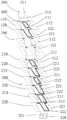
图1为本申请实施例公开的平面变压器的拆解示意图;1 is a schematic diagram of disassembly of a planar transformer disclosed in an embodiment of the present application;
图2为本申请实施例公开的第一PCB板及第二PCB板的剖面示意图;2 is a schematic cross-sectional view of a first PCB board and a second PCB board disclosed in an embodiment of the present application;
图3为本申请实施例公开的另一种形式的平面变压器的示意图;3 is a schematic diagram of another form of a planar transformer disclosed in an embodiment of the application;
图4为本申请实施例公开的采用Rogers 4350与FR-4组合的平面变压器的示意图;4 is a schematic diagram of a planar transformer using a combination of Rogers 4350 and FR-4 disclosed in an embodiment of the application;
图5为本申请实施例公开的第一磁芯(或第二磁芯)的示意图。FIG. 5 is a schematic diagram of a first magnetic core (or a second magnetic core) disclosed in an embodiment of the present application.
附图标记说明:Description of reference numbers:
100-第一PCB板;110-第一初级线路层;111-第一初级绕组;112-第一初级线路层本体;120-第一次级线路层;121-第一次级绕组;122-第一次级线路层本体;131-第一Rogers 4350板材层;140-第一通道;100-first PCB board; 110-first primary circuit layer; 111-first primary winding; 112-first primary circuit layer body; 120-first secondary circuit layer; 121-first secondary winding; 122- The first secondary circuit layer body; 131 - the first Rogers 4350 sheet layer; 140 - the first channel;
200-第二PCB板;210-第二初级线路层;211-第二初级绕组;212-第二初级线路层本体;220-第二次级线路层;221-第二次级绕组;222-第二次级线路层本体;231-第二Rogers 4350板材层;232-FR-4板材层;240-第二通道;200-second PCB board; 210-second primary circuit layer; 211-second primary winding; 212-second primary circuit layer body; 220-second secondary circuit layer; 221-second secondary winding; 222- The second secondary circuit layer body; 231 - the second Rogers 4350 board layer; 232 - the FR-4 board layer; 240 - the second channel;
300-平面磁芯;310-第一磁芯;311-第一连接部;312-窗口;320-第二磁芯;321-第二连接部;300-planar magnetic core; 310-first magnetic core; 311-first connection part; 312-window; 320-second magnetic core; 321-second connection part;
400-电气连接结构。400 - Electrical connection structure.
具体实施方式Detailed ways
下面将结合本申请实施例中的附图,对本申请实施例中的技术方案进行清楚、完整地描述,显然,所描述的实施例是本申请一部分实施例,而不是全部的实施例。基于本申请中的实施例,本领域普通技术人员在没有作出创造性劳动前提下所获得的所有其他实施例,都属于本申请保护的范围。The technical solutions in the embodiments of the present application will be clearly and completely described below with reference to the accompanying drawings in the embodiments of the present application. Obviously, the described embodiments are part of the embodiments of the present application, not all of the embodiments. Based on the embodiments in the present application, all other embodiments obtained by those of ordinary skill in the art without creative work fall within the protection scope of the present application.
本申请的说明书和权利要求书中的术语“第一”、“第二”等是用于区别类似的对象,而不用于描述特定的顺序或先后次序。应该理解这样使用的数据在适当情况下可以互换,以便本申请的实施例能够以除了在这里图示或描述的那些以外的顺序实施,且“第一”、“第二”等所区分的对象通常为一类,并不限定对象的个数,例如第一对象可以是一个,也可以是多个。此外,说明书以及权利要求中“和/或”表示所连接对象的至少其中之一,字符“/”,一般表示前后关联对象是一种“或”的关系。The terms "first", "second" and the like in the description and claims of the present application are used to distinguish similar objects, and are not used to describe a specific order or sequence. It is to be understood that the data so used are interchangeable under appropriate circumstances so that the embodiments of the present application can be practiced in sequences other than those illustrated or described herein, and distinguish between "first", "second", etc. The objects are usually of one type, and the number of objects is not limited. For example, the first object may be one or more than one. In addition, "and/or" in the description and claims indicates at least one of the connected objects, and the character "/" generally indicates that the associated objects are in an "or" relationship.
下面结合附图,通过具体的实施例及其应用场景对本申请实施例进行详细地说明。The embodiments of the present application will be described in detail below through specific embodiments and application scenarios with reference to the accompanying drawings.
参考图1至图5,本申请实施例公开了一种平面变压器,应用于多种电气设备,所公开的平面变压器包括第一PCB板100、第二PCB板200和平面磁芯300。Referring to FIGS. 1 to 5 , an embodiment of the present application discloses a planar transformer, which is applied to various electrical devices. The disclosed planar transformer includes a
其中,第一PCB板100和第二PCB板200均可以包括基材和设置于基材的导线,以通过导线进行电能传输。可选地,导线可以是扁平连续铜制螺旋线,基材可以是印刷电路板,扁平连续铜制螺旋线刻蚀在印刷电路板上。Wherein, both the
第一PCB板100与第二PCB板200叠置,且两者通过平面磁芯300进行固定。基于此,可以通过平面磁芯300保证第一PCB板100与第二PCB板200之间安装的牢固性和稳定性。The
进一步地,为实现走线,第一PCB板100和第二PCB板200均包括多层线路层,每层线路层分别设有绕组,且该绕组可以为初级绕组或次级绕组;在全部线路层中,设有初级绕组的线路层与设有次级绕组的线路层交替设置,且全部线路层的绕组通过串联、并联组合,形成平面变压器的初、次级线圈(即,初级线圈和次级线圈),以实现电能的传输和转换。此处需要说明的是,多层线路层之间可以通过粘接的方式固定,如,采用树脂类粘合剂进行粘接,当然,还可以是其他固定方式,本申请实施例对此不作具体限制。另外,全部线路层的绕组的连接方式将在下述内容中进行详细阐述。Further, in order to realize wiring, both the
根据电磁感应原理,当初级线圈中通入交变电流时,其在初级线圈周围可以产生交变磁场,交变磁场使次级线圈中的磁通量发生变化,使次级线圈中产生感应电动势,从而可以使电能从初级线圈向次级线圈传输,实现平面变压器功能。According to the principle of electromagnetic induction, when an alternating current is passed into the primary coil, an alternating magnetic field can be generated around the primary coil, and the alternating magnetic field changes the magnetic flux in the secondary coil, causing an induced electromotive force in the secondary coil, thereby The electrical energy can be transmitted from the primary coil to the secondary coil to realize the function of a planar transformer.
另外,考虑到感应电动势的大小受到初级线圈与次级线圈之间的匝数比影响。基于此,为了调节感应电动势的大小,可以适当增大或减小初级线圈与次级线圈之间的匝数比,以增大感应电动势或减小感应电动势,从而满足不同工况下对于感应电动势的需求。In addition, it is considered that the magnitude of the induced electromotive force is affected by the turns ratio between the primary coil and the secondary coil. Based on this, in order to adjust the size of the induced electromotive force, the turns ratio between the primary coil and the secondary coil can be appropriately increased or decreased to increase the induced electromotive force or reduce the induced electromotive force, so as to meet the requirements for the induced electromotive force under different working conditions. demand.
基于上述设置,本申请实施例中的平面变压器包括相互层叠设置的第一PCB板100和第二PCB板200,且两者各自包括多层线路层,每一层线路层设有初级绕组或次级绕组,在布置各层线路层时,使设有初级绕组的线路层与设有次级绕组的线路层交替设置,从而可以实现初、次级绕组的交织走线,以形成交织走线的初级线圈和次级线圈。由此可知,此种方式无需在线路层之间设置绝缘层,相比于多个PCB板之间通过独立绝缘层隔离的方式,本申请实施例中的平面变压器可以尽可能地减小初级绕组与次级绕组之间的间隙,从而可以有效缓解磁力线通过间隙向四周扩散的问题,进而可以使漏感降低,克服漏磁问题,以提升平面变压器的性能。Based on the above settings, the planar transformer in the embodiment of the present application includes a
本申请实施例中的平面变压器以第二PCB板200为基板,可以将至少一个第一PCB板100层叠设置在第二PCB板200上,相比于单独的PCB板,在平面磁芯300的窗口312的面积不变的情况下,可以增大绕组的横截面积,从而可以提高对于平面磁芯300的窗口312的利用率。The planar transformer in the embodiment of the present application uses the
此处需要说明的是,平面磁芯300的窗口312的利用率是指平面变压器中绕组的单一导线的横截面积*匝数/窗口面积。如图5所示,以EI型平面磁芯300为例,窗口面积是指F*(E-D)/2,其中,F为窗口312的宽度,(E-D)/2为窗口312的高度;单一导线的横截面积为线宽*厚度*匝数。基于此,可以计算出平面磁芯300的窗口312的利用率。It should be noted here that the utilization rate of the
由此可见,相比于单独的PCB板,本申请实施例中,通过至少一个第一PCB板100和第二PCB板200共同组成的平面变压器中绕组的总的横截面积更大,进而可以提高平面磁芯300的窗口312的利用率。It can be seen that, compared with a single PCB board, in the embodiment of the present application, the total cross-sectional area of the windings in the planar transformer formed by the at least one
参考图1和图2,在一些实施例中,第一PCB板100可以包括层叠设置的第一初级线路层110和第一次级线路层120,其中,第一初级线路层110设有第一初级绕组111,第一次级线路层120设有第一次级绕组121,且第一初级绕组111与第二次级绕组221相互适配。基于此,一方面,第一初级绕组111与第一次级绕组121之间可以进行电能的传输,另一方面,通过第一初级线路层110与第一次级线路层120层叠设置,可以使第一初级绕组111与第一次级绕组121之间的间隙尽可能减小,从而可以减少第一初级绕组111与第一次级绕组121之间的磁力线向四周扩散而导致的漏感,进而有利于提升平面变压器的性能。Referring to FIG. 1 and FIG. 2 , in some embodiments, the
可选地,第一初级线路层110可以包括第一初级线路层本体112,第一初级绕组111可以设置于第一初级线路层本体112上,以通过第一初级线路层本体112实现对第一初级绕组111的安装和固定。同样地,第一次级线路层120可以包括第一次级线路层本体122,第一次级绕组121可以设置于第一次级线路层本体122上,以通过第一次级线路层本体122实现对第一次级绕组121的安装和固定。Optionally, the first
同理,第二PCB板200可以包括层叠设置的第二初级线路层210和第二次级线路层220,其中,第二初级线路层210设有第二初级绕组211,第二次级线路层220设有第二次级绕组221,且第二初级绕组211与第二次级绕组221对应设置。基于此,一方面,第二初级绕组211与第二次级绕组221之间可以进行电能的传输,另一方面,通过第二初级线路层210与第二次级线路层220层叠设置,可以使第二初级绕组211与第二次级绕组221之间的间隙尽可能减小,从而可以减少第二初级绕组211与第二次级绕组221之间的磁力线向四周扩散而导致的漏感,进而有利于提升平面变压器的性能。Similarly, the
可选地,第二初级线路层210可以包括第二初级线路层本体212,第二初级绕组211可以设置于第二初级线路层本体212上,以通过第二初级线路层本体212实现对第二初级绕组211的安装和固定。同样地,第二次级线路层220可以包括第二次级线路层本体222,第二次级绕组221可以设置于第二次级线路层本体222上,以通过第二次级线路层本体222实现对第二次级绕组221的安装和固定。Optionally, the second
进一步地,在配置第一PCB板100与第二PCB板200时,第一初级线路层110、第一次级线路层120、第二初级线路层210和第二次级线路层220依次层叠设置。基于此,使第一初级绕组111、第一次级绕组121、第二初级绕组211和第二次级绕组221依次设置,从而形成了初级绕组与次级绕组的交替设置。基于此,一方面实现了第一PCB板100与第二PCB板200的叠置,以便于形成平面变压器,另一方面还可以减小初级绕组与次级绕组之间的间隙,从而可以缓解漏磁,降低漏感,进而可以提升平面变压器性能。Further, when configuring the
本申请实施例中,第一初级绕组111与第二初级绕组211串联,第一次级绕组121与第二次级绕组221并联。如此,通过串联、并联组合,可以分别形成平面变压器的初级线圈和次级线圈,以便于通过初级线圈与次级线圈之间的电磁感应而实现电能的传输。In the embodiment of the present application, the first primary winding 111 is connected in series with the second primary winding 211 , and the first secondary winding 121 is connected in parallel with the second secondary winding 221 . In this way, through the combination of series and parallel, the primary coil and the secondary coil of the planar transformer can be formed respectively, so as to realize the transmission of electric energy through the electromagnetic induction between the primary coil and the secondary coil.
可选地,当第一初级绕组111缠绕两匝,第二初级绕组211缠绕两匝,第一次级绕组121缠绕一匝,第二次级绕组221缠绕一匝时,通过计算可知,由第一初级绕组111和第二初级绕组211串联形成的初级线圈,与由第一次级绕组121和第二次级绕组221并联形成的次级线圈可以使平面变压器的变比为4:1,以满足实际工况的需求。当然,还可以通过改变各个绕组的匝数来调整平面变压器的变比,以满足不同工况的需求。Optionally, when the first primary winding 111 is wound with two turns, the second primary winding 211 is wound with two turns, the first secondary winding 121 is wound with one turn, and the second secondary winding 221 is wound with one turn, it can be known by calculation that the first A primary coil formed by the primary winding 111 and the second primary winding 211 in series, and the secondary coil formed by the first secondary winding 121 and the second secondary winding 221 in parallel can make the transformation ratio of the planar transformer 4:1, so that the Meet the needs of actual working conditions. Of course, the transformation ratio of the planar transformer can also be adjusted by changing the number of turns of each winding to meet the needs of different working conditions.
在一些实施例中,第一PCB板100可以包括多对相互配合的第一初级线路层110和第一次级线路层120,且多对中的第一初级线路层110与第一次级线路层120交替设置。如此,每对中第一初级线路层110设有的第一初级绕组111与第一次级线路层120设有的第一次级绕组121之间能够通过电磁感应形成感应电动势,以便于在第一PCB板100的初级与次级之间进行电能传输。In some embodiments, the
同样地,第二PCB板200可以包括多对相互配合的第二初级线路层210和第二次级线路层220,且多对中的第二初级线路层210与第二次级线路层220交替设置。如此,每对中的第二初级线路层210设有的第二初级绕组211与第二次级线路层220设有的第二次级绕组221之间能够通过电磁感应形成感应电动势,以便于在第二PCB板200的初级与次级之间进行电能传输。Likewise, the
由于第一PCB板100与第二PCB板200层叠设置,使得在第一PCB板100和第二PCB板200的连接处,位于第一PCB板100的一侧的第一次级线路层120与位于第二PCB板200的一侧的第二初级线路层210连接。基于此,在第一PCB板100与第二PCB板200两者所包括的全部线路层中,可以实现初级绕组与次级绕组依次交替设置,且初级绕组与次级绕组之间不存在绝缘层进行隔离,从而可以减小初级绕组与次级绕组之间的距离,进而可以减少漏感,以提升平面变压器的性能。Since the
参考图3,在一种较为具体的实施例中,第一PCB板100可以包括两对相互配合的第一初级线路层110和第一次级线路层120,也即,第一PCB板100包括四层线路层,且四层线路层的绕组的配置方式为:初级绕组、次级绕组、初级绕组和次级绕组。第二PCB板200可以包括三对相互配合的第二初级线路层210和第二次级线路层220,也即,第二PCB板200包括六层线路层,且六层线路层的绕组的配置方式为:初级绕组、次级绕组、初级绕组、次级绕组、初级绕组和次级绕组。如此,整个平面变压器中的绕组的配置方式为:初级绕组、次级绕组、初级绕组、次级绕组、初级绕组、次级绕组、初级绕组、次级绕组、初级绕组和次级绕组,并且,五组初级绕组依次串联,五组次级绕组相互并联。当初级绕组缠绕两匝,次级绕组缠绕一匝时,可以形成变比为10:1的平面变压器,以便于满足实际工况的需求。Referring to FIG. 3 , in a more specific embodiment, the
基于上述设置,本申请实施例可以通过调节第一PCB板100所包括的相互配合的第一初级线路层110和第一次级线路层120的对数,和/或,通过调节第二PCB板200所包括的第二初级线路层210和第二次级线路层220的对数,便可以调节整个平面变压器的变比,以便于满足不同工况的需求,从而可以提高平面变压器的适用性。Based on the above settings, in this embodiment of the present application, the number of pairs of the first
并且,相比于第一PCB板100和第二PCB板200各自包括一对的方式,在达到同样变比的情况下,可以减小初级线圈与次级线圈之间的匝数比,从而可以缓解匝数比过大而导致平面变压器过热的问题。In addition, compared with the way in which the
为了进一步提高平面变压器的性能,一些实施例中,相邻两层线路层中的其中一者设有初级绕组,另一者设有次级绕组,且初级绕组与次级绕组对齐设置。基于此,在初级绕组通电后,其产生的磁通使初级绕组与次级绕组之间更容易产生电磁感应,从而使平面变压器的运行更加高效,进而可以提升平面变压器的性能。In order to further improve the performance of the planar transformer, in some embodiments, one of the adjacent two circuit layers is provided with a primary winding, and the other is provided with a secondary winding, and the primary winding and the secondary winding are arranged in alignment. Based on this, after the primary winding is energized, the magnetic flux generated by it makes it easier to generate electromagnetic induction between the primary winding and the secondary winding, so that the operation of the planar transformer is more efficient, and the performance of the planar transformer can be improved.
在一些实施例中,平面变压器可以包括多个第一PCB板100和一个第二PCB板200,其中,多个第一PCB板100依次层叠设置,且位于端部的第一PCB板100与第二PCB板200连接。此处需要说明的是,第二PCB板200可以作为基板(即,基础安装结构),其用于设置第一PCB板100,以实现对第一PCB板100的安装和支撑作用。In some embodiments, the planar transformer may include a plurality of
基于上述设置,将多个依次层叠设置的第一PCB板100设置于第二PCB板200,可以适当增加平面变压器的厚度;当第一PCB板100和第二PCB板200均包括多层线路层时,可以增加所有线路层的绕组在平面变压器厚度方向上的尺寸,从而可以在不增加平面磁芯300的窗口312的情况下,增大绕组的横截面积,进而可以增加平面磁芯300的窗口312的利用率。Based on the above arrangement, the thickness of the planar transformer can be appropriately increased by arranging a plurality of
本申请实施例中,第一PCB板100可以单独成型制作,第二PCB板200同样可以单独成型制作,而后将两个成型结构通过平面磁芯300装配在一起,以形成平面变压器。相比于平面变压器的所有层结构一并装配的方式,本申请实施例中采用分别成型而后装配的方式可以降低装配误差,提高平面变压器的一致性。In the embodiment of the present application, the
在一些实施例中,第一PCB板100的线路层可以为第一Rogers 4350板材层131,也即,该线路层采用Rogers 4350材质,第一初级绕组111或第一次级绕组121可以设置于第一Rogers 4350板材层131。此处需要说明的是,Rogers4350材质具有较低的相对介电常数和低介质损耗因数,如此,通过采用第一Rogers 4350板材层131,使得射频信号走线在第一Rogers 4350板材层131上时,可以减小传输损耗,减小传输延迟,且有利于射频信号的传输和线路层整体阻抗控制,从而可以增加射频传输性能,有利于提高平面变压器的性能。除此以外,第一PCB板100的线路层还可以采用其他材质的板材层,只要满足要求即可,具体材质不受限制。In some embodiments, the circuit layer of the
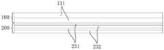
参考图4,第二PCB板200的线路层可以包括第二Rogers 4350板材层231和FR-4板材层232,且第二Rogers 4350板材层231与FR-4板材层232层叠设置,而第二初级绕组211或第二次级绕组221可以设置于第二Rogers 4350板材层231。此处需要说明的是,Rogers4350具有较低的相对介电常数和低介质损耗因数,FR-4具有较高的机械强度,如此,通过采用第二Rogers 4350板材层231与FR-4板材层232的组合,使得射频信号走线在第二Rogers4350板材层231上时,有利于射频信号的传输和线路层整体阻抗控制,且减少传输损耗,与此同时,通过FR-4板材层232可以提高线路层的机械强度,以防止线路层损坏。除此以外,第二PCB板200的线路层还可以采用其他材质的板材层或多种材质层的组合,只要满足要求即可,具体材质不受限制。Referring to FIG. 4 , the circuit layer of the
基于上述设置,相比于仅由FR-4材质的PCB组成的平面变压器,本申请实施例中由第一PCB板100和第二PCB板200共同组成的平面变压器可以对高频信号(如,MHz以上)具有更好的传输效果。Based on the above settings, compared to a planar transformer composed of only a PCB made of FR-4 material, the planar transformer composed of the
为缓解漏磁问题,一些实施例中,相邻的两层线路层之间的距离小于线路层的厚度。基于此,相比于线路层之间通过绝缘层隔离的方式,本申请实施例中无需额外设置绝缘层,从而可以最大限度的减小相邻两层线路层之间的间隙,有利于减少磁力线通过间隙空间向四周扩散,减少漏磁,进而可以降低漏感,提高平面变压器的性能。To alleviate the magnetic flux leakage problem, in some embodiments, the distance between two adjacent circuit layers is smaller than the thickness of the circuit layers. Based on this, compared with the method of separating circuit layers by insulating layers, there is no need to provide an additional insulating layer in the embodiment of the present application, so that the gap between two adjacent circuit layers can be minimized, which is beneficial to reduce the magnetic lines of force The gap space is diffused around to reduce magnetic flux leakage, thereby reducing leakage inductance and improving the performance of the planar transformer.
此处需要说明的是,为避免相邻的两层线路层之间出现短路现象,可以对每层线路层的表面做绝缘处理,可选地,在线路层的表面涂覆一层绝缘薄膜,通过绝缘薄膜既可以起到绝缘作用,又不至于额外增加绝缘层,如此,可以在保证平面变压器正常工作的情况下提升性能。It should be noted here that, in order to avoid short circuit between two adjacent circuit layers, the surface of each circuit layer can be insulated. Optionally, a layer of insulating film is coated on the surface of the circuit layer. The insulating film can play an insulating role without adding an additional insulating layer. In this way, the performance of the planar transformer can be improved while ensuring the normal operation of the planar transformer.
参考图1,为了对第一PCB板100和第二PCB板200进行固定,平面磁芯300可以包括第一磁芯310和第二磁芯320,通过第一磁芯310和第二磁芯320的配合,可以对将第一PCB板100与第二PCB板200牢牢固定,以保证平面变压器的整体强度。Referring to FIG. 1 , in order to fix the
进一步地,第一PCB板100设有第一通道140,第二PCB板200设有第二通道240,相应地,第一磁芯310设有第一连接部311,第一连接部311穿设于第一通道140中,第二连接部321穿设于第二通道240中,且第一连接部311与所述第二连接部321连接。基于此,通过第一连接部311与第一通道140的配合,以及第二连接部321与第二通道240的配合,可以有效防止第一PCB板100与第二PCB板200相对移动,从而提高了第一PCB板100与第二PCB板200之间装配的牢固性和稳定性,进而保证了平面变压器的整体强度。此处需要说明的是,该种平面磁芯300可以为EE型磁芯。Further, the
可选地,第一磁芯310可以设有凸起结构,该凸起结构作为第一连接部311,第二磁芯320可以设有凸起结构,该凸起结构作为第二连接部321,如此,通过凸起结构与第一通道140或第二通道240配合可以保证配合的稳定性。Optionally, the first
为进一步提高装配牢固性和稳定性,第一磁芯310可以设有多个第一连接部311,第二磁芯320可以设有多个第二连接部321,且第一连接部311与第二连接部321相互对应。相应地,第一PCB板100可以设有多个第一通道140,第二PCB板200可以设有多个第二通道240。如此,通过多个第一连接部311与多个第一通道140配合,以及通过多个第二连接部321与多个第二通道240配合,增加了平面磁芯300与第一PCB板100及第二PCB板200的装配面积,从而可以提高装配牢固性和稳定性,进而可以提高平面变压器的整体强度。In order to further improve the assembly firmness and stability, the first
在其他一些实施例中,第一磁芯310可以设有第一连接部311,第一连接部311穿设于第一通道140和第二通道240中,且第一磁芯310与第二磁芯320连接。基于此,通过第一连接部311与第一通道140及第二通道240分别配合,以防止第一PCB板100与第二PCB板200相对移动,此种方式同样可以提高平面变压器的整体强度。此处需要说明的是,该种平面磁芯300可以为EI型磁芯。In some other embodiments, the first
当然,除了上述形式的平面磁芯300之外,还可以采用其他形式,只要能够固定第一PCB板100和第二PCB板200即可,具体方式不受限制。Of course, in addition to the planar
为实现第一磁芯310与第二磁芯320之间的连接,一些实施例中,第一磁芯310与第二磁芯320之间可以固定连接,可选地,可以利用粘合剂粘接,以保证连接的牢固性。当然,为了便于维修,第一磁芯310与第二磁芯320之间还可以采用可拆卸方式连接,可选地,可以采用卡接方式、螺接方式等进行连接,以便于拆装,从而可以便于对平面变压器进行维修。In order to realize the connection between the first
考虑到第一PCB板100包括多层线路层,为了形成第一通道140,每层线路层分别设有通孔,且多层线路层的通孔依次连通,形成第一通道140。基于此,在第一连接部311穿设至第一通道140中的情况下,第一连接部311的外壁可以与各层线路层的通孔的内壁抵接,从而可以通过第一连接部311限制每一层线路层移动,以提高第一PCB板100装配的稳定性和牢固性;与此同时,还可以防止第一PCB板100的初级绕组与次级绕组相互错位而影响电能传输,从而有利于提升平面变压器的性能。Considering that the
同样地,考虑到第二PCB板200包括多层线路层,为了形成第二通道240,每层线路层分别设有通孔,且多层线路层的通孔依次连通,形成第二通道240。基于此,在第二连接部321穿设至第二通道240中的情况下,第二连接部321的外壁可以与各个线路层的通孔的内壁抵接,从而可以通过第二连接部321限制每一层线路层移动,以提高第二PCB板200装配的稳定性和牢固性;与此同时,还可以防止第二PCB板200的初级绕组与次级绕组相互错位而影响电能传输,从而有利于提升平面变压器的性能。Similarly, considering that the
在一些实施例中,每层线路层的通孔的周围绕设至少一匝绕组。基于此,可以使相邻的线路层各自的绕组相对设置,最大程度地减小相邻两层线路层的绕组之间的距离,从而可以使相邻两层线路层之间传输电能的最大化,进而提升平面变压器的性能。In some embodiments, at least one turn of winding is arranged around the perimeter of the through hole of each wiring layer. Based on this, the respective windings of the adjacent circuit layers can be arranged opposite to each other, and the distance between the windings of the adjacent two circuit layers can be minimized, thereby maximizing the transmission of electrical energy between the two adjacent circuit layers. , thereby improving the performance of the planar transformer.
为了实现各线路层之间的电性连接,以分别形成初级线圈、次级线圈,以及与外部其他电气件连接,线路层可以设有电气连接结构400,通过电气连接结构400可以将不同的线路层之间电性连接,或者将线路层与外界电气件连接,以便于进行电能传输。In order to realize the electrical connection between the circuit layers, to form the primary coil, the secondary coil, and to connect with other external electrical components, the circuit layer can be provided with an
可选地,电气连接结构400可以包括焊接孔位、焊盘和焊点中的至少一者。基于此,可以提高连接的牢固性,且可以保证电性连接良好,以避免出现虚接现象而影响平面变压器正常工作。除此以外,电气连接结构400还可以为其他形式,本申请实施例对此不作具体限定。Optionally, the
综上所述,本申请实施例中的平面变压器通过采用Rogers 4350和FR-4的组合,在射频应用中可以提升射频传输性能,并且提高线路层的机械强度;采用在第二PCB板200之外增加独立的第一PCB板100的方式,相比于以往产品,在一定程度上可以提升平面磁芯300的窗口312的利用率,并且可以分别制作第一PCB板100和第二PCB板200,而后装配,从而可以降低装配误差,提高平面变压器的一致性;通过初级绕组与次级绕组交替设置,形成交织走线,在一定程度上可以降低平面变压器的漏感。To sum up, by using the combination of Rogers 4350 and FR-4, the planar transformer in the embodiment of the present application can improve the radio frequency transmission performance and improve the mechanical strength of the circuit layer in radio frequency applications; The method of adding an independent
上面结合附图对本申请的实施例进行了描述,但是本申请并不局限于上述的具体实施方式,上述的具体实施方式仅仅是示意性的,而不是限制性的,本领域的普通技术人员在本申请的启示下,在不脱离本申请宗旨和权利要求所保护的范围情况下,还可做出很多形式,均属于本申请的保护之内。The embodiments of the present application have been described above in conjunction with the accompanying drawings, but the present application is not limited to the above-mentioned specific embodiments, which are merely illustrative rather than restrictive. Under the inspiration of this application, without departing from the scope of protection of the purpose of this application and the claims, many forms can be made, which all fall within the protection of this application.
Claims (10)
Priority Applications (1)
| Application Number | Priority Date | Filing Date | Title |
|---|---|---|---|
| CN202210528729.0ACN114864239A (en) | 2022-05-16 | 2022-05-16 | Planar transformer |
Applications Claiming Priority (1)
| Application Number | Priority Date | Filing Date | Title |
|---|---|---|---|
| CN202210528729.0ACN114864239A (en) | 2022-05-16 | 2022-05-16 | Planar transformer |
Publications (1)
| Publication Number | Publication Date |
|---|---|
| CN114864239Atrue CN114864239A (en) | 2022-08-05 |
Family
ID=82637594
Family Applications (1)
| Application Number | Title | Priority Date | Filing Date |
|---|---|---|---|
| CN202210528729.0APendingCN114864239A (en) | 2022-05-16 | 2022-05-16 | Planar transformer |
Country Status (1)
| Country | Link |
|---|---|
| CN (1) | CN114864239A (en) |
Citations (3)
| Publication number | Priority date | Publication date | Assignee | Title |
|---|---|---|---|---|
| US20020057171A1 (en)* | 2000-02-01 | 2002-05-16 | Patel Raoji A. | Apparatus and method for pcb winding planar magnetic devices |
| US20060038649A1 (en)* | 2004-08-19 | 2006-02-23 | Rockwell Scientific Licensing, Llc | Winding structure for efficient switch-mode power converters |
| CN205789425U (en)* | 2016-05-31 | 2016-12-07 | 深圳市麦吉瑞科技有限公司 | A kind of flat surface transformer |
- 2022
- 2022-05-16CNCN202210528729.0Apatent/CN114864239A/enactivePending
Patent Citations (3)
| Publication number | Priority date | Publication date | Assignee | Title |
|---|---|---|---|---|
| US20020057171A1 (en)* | 2000-02-01 | 2002-05-16 | Patel Raoji A. | Apparatus and method for pcb winding planar magnetic devices |
| US20060038649A1 (en)* | 2004-08-19 | 2006-02-23 | Rockwell Scientific Licensing, Llc | Winding structure for efficient switch-mode power converters |
| CN205789425U (en)* | 2016-05-31 | 2016-12-07 | 深圳市麦吉瑞科技有限公司 | A kind of flat surface transformer |
Similar Documents
| Publication | Publication Date | Title |
|---|---|---|
| US6927661B2 (en) | Planar transformer and output inductor structure with single planar winding board and two magnetic cores | |
| US8502633B2 (en) | Planar transformer and method of manufacturing the same | |
| US6373736B2 (en) | Isolated converter | |
| CN108335879B (en) | Planar transformer, electronic equipment and manufacturing method of planar transformer | |
| CN102103923A (en) | Planar transformer | |
| US11120936B2 (en) | Magnetic component module | |
| US7342477B2 (en) | Inductor | |
| CN110970210A (en) | transformer | |
| US10178758B2 (en) | Printed wiring board and method of producing the same | |
| IL156426A (en) | Choke coil | |
| JP2002270437A (en) | Flat coil and flat transformer | |
| CN202695101U (en) | Assembled planar transformer | |
| JPH11307367A (en) | Thin transformer | |
| CN114121465B (en) | Planar transformer | |
| JP4678563B2 (en) | Multilayer type common mode choke coil | |
| JPH10163039A (en) | Thin transformer | |
| CN212113411U (en) | A Planar Transformer with Multiple Outputs on a Multilayer Board | |
| CN106373733B (en) | A kind of adjustable flat surface transformer and its manufacture method | |
| CN114864239A (en) | Planar transformer | |
| JP5311462B2 (en) | Multi-layer substrate transformer | |
| CN218918608U (en) | Planar transformer, power conversion circuit and adapter | |
| CN112740343A (en) | Balanced symmetrical coil | |
| CN201765928U (en) | High isolation planar transformer | |
| CN114974802A (en) | Magnetic device, resonant circuit and LED driving power supply | |
| CN219418735U (en) | Planar transformer and power converter |
Legal Events
| Date | Code | Title | Description |
|---|---|---|---|
| PB01 | Publication | ||
| PB01 | Publication | ||
| SE01 | Entry into force of request for substantive examination | ||
| SE01 | Entry into force of request for substantive examination |