CN114863966A - Integrated circuit, memory circuit, method for forming integrated circuit and method for forming memory circuit - Google Patents
Integrated circuit, memory circuit, method for forming integrated circuit and method for forming memory circuitDownload PDFInfo
- Publication number
- CN114863966A CN114863966ACN202111313549.2ACN202111313549ACN114863966ACN 114863966 ACN114863966 ACN 114863966ACN 202111313549 ACN202111313549 ACN 202111313549ACN 114863966 ACN114863966 ACN 114863966A
- Authority
- CN
- China
- Prior art keywords
- conductive
- regions
- wider
- directly
- individual
- Prior art date
- Legal status (The legal status is an assumption and is not a legal conclusion. Google has not performed a legal analysis and makes no representation as to the accuracy of the status listed.)
- Pending
Links
- 238000000034methodMethods0.000titleclaimsabstractdescription39
- 239000004020conductorSubstances0.000claimsabstractdescription84
- 239000000758substrateSubstances0.000claimsabstractdescription26
- 238000000059patterningMethods0.000claimsabstractdescription11
- 239000000463materialSubstances0.000claimsdescription102
- 230000000873masking effectEffects0.000claimsdescription24
- 238000010276constructionMethods0.000claimsdescription18
- 239000003990capacitorSubstances0.000claimsdescription17
- 238000003860storageMethods0.000claimsdescription14
- VYPSYNLAJGMNEJ-UHFFFAOYSA-NSilicium dioxideChemical compoundO=[Si]=OVYPSYNLAJGMNEJ-UHFFFAOYSA-N0.000description14
- 239000002019doping agentSubstances0.000description13
- 239000012212insulatorSubstances0.000description11
- 239000004065semiconductorSubstances0.000description11
- 239000000203mixtureSubstances0.000description9
- 229910052581Si3N4Inorganic materials0.000description8
- HQVNEWCFYHHQES-UHFFFAOYSA-Nsilicon nitrideChemical compoundN12[Si]34N5[Si]62N3[Si]51N64HQVNEWCFYHHQES-UHFFFAOYSA-N0.000description8
- 230000010287polarizationEffects0.000description7
- 239000000377silicon dioxideSubstances0.000description7
- 235000012239silicon dioxideNutrition0.000description6
- 229910052751metalInorganic materials0.000description5
- 239000002184metalSubstances0.000description5
- 230000015572biosynthetic processEffects0.000description4
- 230000005669field effectEffects0.000description4
- 238000004519manufacturing processMethods0.000description4
- 239000007769metal materialSubstances0.000description4
- 238000003491arrayMethods0.000description3
- 238000000151depositionMethods0.000description3
- 239000011810insulating materialSubstances0.000description3
- 230000008569processEffects0.000description3
- 230000009471actionEffects0.000description2
- 229910045601alloyInorganic materials0.000description2
- 239000000956alloySubstances0.000description2
- 238000000429assemblyMethods0.000description2
- 230000000712assemblyEffects0.000description2
- 125000004429atomChemical group0.000description2
- 238000005530etchingMethods0.000description2
- 230000012010growthEffects0.000description2
- 230000014759maintenance of locationEffects0.000description2
- 150000002739metalsChemical class0.000description2
- 230000002093peripheral effectEffects0.000description2
- 238000005498polishingMethods0.000description2
- 229910021420polycrystalline siliconInorganic materials0.000description2
- 230000002441reversible effectEffects0.000description2
- 229910052707rutheniumInorganic materials0.000description2
- 125000006850spacer groupChemical group0.000description2
- 229910052721tungstenInorganic materials0.000description2
- ITWBWJFEJCHKSN-UHFFFAOYSA-N1,4,7-triazonaneChemical compoundC1CNCCNCCN1ITWBWJFEJCHKSN-UHFFFAOYSA-N0.000description1
- 229910001218Gallium arsenideInorganic materials0.000description1
- 229910000577Silicon-germaniumInorganic materials0.000description1
- ATJFFYVFTNAWJD-UHFFFAOYSA-NTinChemical compound[Sn]ATJFFYVFTNAWJD-UHFFFAOYSA-N0.000description1
- 230000002411adverseEffects0.000description1
- VXAUWWUXCIMFIM-UHFFFAOYSA-Maluminum;oxygen(2-);hydroxideChemical compound[OH-].[O-2].[Al+3]VXAUWWUXCIMFIM-UHFFFAOYSA-M0.000description1
- 238000000231atomic layer depositionMethods0.000description1
- 229910052790berylliumInorganic materials0.000description1
- 229910002056binary alloyInorganic materials0.000description1
- 230000001413cellular effectEffects0.000description1
- 238000003486chemical etchingMethods0.000description1
- 238000005229chemical vapour depositionMethods0.000description1
- 229910052681coesiteInorganic materials0.000description1
- 238000004891communicationMethods0.000description1
- 150000001875compoundsChemical class0.000description1
- 229910052802copperInorganic materials0.000description1
- 230000008878couplingEffects0.000description1
- 238000010168coupling processMethods0.000description1
- 238000005859coupling reactionMethods0.000description1
- 229910052906cristobaliteInorganic materials0.000description1
- 238000013500data storageMethods0.000description1
- 230000008021depositionEffects0.000description1
- 239000003989dielectric materialSubstances0.000description1
- 238000009792diffusion processMethods0.000description1
- 230000000694effectsEffects0.000description1
- 230000005684electric fieldEffects0.000description1
- 239000012777electrically insulating materialSubstances0.000description1
- 239000012634fragmentSubstances0.000description1
- 230000006870functionEffects0.000description1
- 229910000449hafnium oxideInorganic materials0.000description1
- WIHZLLGSGQNAGK-UHFFFAOYSA-Nhafnium(4+);oxygen(2-)Chemical compound[O-2].[O-2].[Hf+4]WIHZLLGSGQNAGK-UHFFFAOYSA-N0.000description1
- 229910052736halogenInorganic materials0.000description1
- 125000005843halogen groupChemical group0.000description1
- 238000005468ion implantationMethods0.000description1
- 238000002955isolationMethods0.000description1
- 150000002736metal compoundsChemical class0.000description1
- 230000004048modificationEffects0.000description1
- 238000012986modificationMethods0.000description1
- 229910052750molybdenumInorganic materials0.000description1
- 229910021421monocrystalline siliconInorganic materials0.000description1
- 150000004767nitridesChemical class0.000description1
- 230000003071parasitic effectEffects0.000description1
- 238000000206photolithographyMethods0.000description1
- 229920002120photoresistant polymerPolymers0.000description1
- 238000005240physical vapour depositionMethods0.000description1
- 229920005591polysiliconPolymers0.000description1
- 229910052682stishoviteInorganic materials0.000description1
- 239000000126substanceSubstances0.000description1
- 229910052715tantalumInorganic materials0.000description1
- 229910052719titaniumInorganic materials0.000description1
- 229910052905tridymiteInorganic materials0.000description1
- 239000011800void materialSubstances0.000description1
Images


Classifications
- H—ELECTRICITY
- H10—SEMICONDUCTOR DEVICES; ELECTRIC SOLID-STATE DEVICES NOT OTHERWISE PROVIDED FOR
- H10B—ELECTRONIC MEMORY DEVICES
- H10B12/00—Dynamic random access memory [DRAM] devices
- H10B12/30—DRAM devices comprising one-transistor - one-capacitor [1T-1C] memory cells
- H10B12/31—DRAM devices comprising one-transistor - one-capacitor [1T-1C] memory cells having a storage electrode stacked over the transistor
- H10B12/315—DRAM devices comprising one-transistor - one-capacitor [1T-1C] memory cells having a storage electrode stacked over the transistor with the capacitor higher than a bit line
- G—PHYSICS
- G11—INFORMATION STORAGE
- G11C—STATIC STORES
- G11C8/00—Arrangements for selecting an address in a digital store
- G11C8/08—Word line control circuits, e.g. drivers, boosters, pull-up circuits, pull-down circuits, precharging circuits, for word lines
- H—ELECTRICITY
- H10—SEMICONDUCTOR DEVICES; ELECTRIC SOLID-STATE DEVICES NOT OTHERWISE PROVIDED FOR
- H10B—ELECTRONIC MEMORY DEVICES
- H10B12/00—Dynamic random access memory [DRAM] devices
- H10B12/01—Manufacture or treatment
- H10B12/02—Manufacture or treatment for one transistor one-capacitor [1T-1C] memory cells
- H10B12/03—Making the capacitor or connections thereto
- H10B12/033—Making the capacitor or connections thereto the capacitor extending over the transistor
- H10B12/0335—Making a connection between the transistor and the capacitor, e.g. plug
- H—ELECTRICITY
- H10—SEMICONDUCTOR DEVICES; ELECTRIC SOLID-STATE DEVICES NOT OTHERWISE PROVIDED FOR
- H10B—ELECTRONIC MEMORY DEVICES
- H10B12/00—Dynamic random access memory [DRAM] devices
- H10B12/01—Manufacture or treatment
- H10B12/02—Manufacture or treatment for one transistor one-capacitor [1T-1C] memory cells
- H10B12/05—Making the transistor
- H10B12/053—Making the transistor the transistor being at least partially in a trench in the substrate
- H—ELECTRICITY
- H10—SEMICONDUCTOR DEVICES; ELECTRIC SOLID-STATE DEVICES NOT OTHERWISE PROVIDED FOR
- H10B—ELECTRONIC MEMORY DEVICES
- H10B12/00—Dynamic random access memory [DRAM] devices
- H10B12/30—DRAM devices comprising one-transistor - one-capacitor [1T-1C] memory cells
- H10B12/34—DRAM devices comprising one-transistor - one-capacitor [1T-1C] memory cells the transistor being at least partially in a trench in the substrate
- H—ELECTRICITY
- H10—SEMICONDUCTOR DEVICES; ELECTRIC SOLID-STATE DEVICES NOT OTHERWISE PROVIDED FOR
- H10B—ELECTRONIC MEMORY DEVICES
- H10B12/00—Dynamic random access memory [DRAM] devices
- H10B12/30—DRAM devices comprising one-transistor - one-capacitor [1T-1C] memory cells
- H10B12/48—Data lines or contacts therefor
- H10B12/482—Bit lines
Landscapes
- Engineering & Computer Science (AREA)
- Manufacturing & Machinery (AREA)
- Microelectronics & Electronic Packaging (AREA)
- Semiconductor Memories (AREA)
Abstract
Description
Translated fromChinese技术领域technical field
本文中所公开的实施例涉及集成电路、存储器电路、用于形成集成电路的方法以及用于形成存储器电路的方法。Embodiments disclosed herein relate to integrated circuits, memory circuits, methods for forming integrated circuits, and methods for forming memory circuits.
背景技术Background technique
存储器是一种类型的集成电路且在计算机系统中用于存储数据。存储器可制造于个别存储器单元的一或多个阵列中。可使用数字线(其也可被称为位线、数据线或感测线)和存取线(其也可被称为字线)对存储器单元进行写入或从中进行读取。数字线可沿阵列的列以导电方式互连存储器单元,且存取线可沿阵列的行以导电方式互连存储器单元。每一存储器单元可通过数字线与存取线的组合进行唯一地寻址。Memory is a type of integrated circuit and is used in computer systems to store data. Memory can be fabricated in one or more arrays of individual memory cells. Memory cells may be written to or read from using digit lines (which may also be referred to as bit lines, data lines, or sense lines) and access lines (which may also be referred to as word lines). Digit lines may conductively interconnect memory cells along columns of the array, and access lines may conductively interconnect memory cells along rows of the array. Each memory cell is uniquely addressable by a combination of digit lines and access lines.
存储器单元可以是易失性的、半易失性的或非易失性的。非易失性存储器单元可在不通电的情况下将数据存储很长一段时间。非易失性存储器通常被指定为具有至少约10年的保留时间的存储器。易失性存储器耗散,且因此刷新/重写以维持数据存储。易失性存储器可具有数毫秒或更短的保留时间。无论如何,存储器单元配置成以至少两个不同可选择状态保持或存储存储器。在二进制系统中,所述状态被视为“0”或“1”。在其它系统中,至少一些个别存储器单元可配置成存储多于两个层级或状态的信息。Memory cells can be volatile, semi-volatile or non-volatile. Non-volatile memory cells can store data for long periods of time without powering up. Non-volatile memory is typically designated as memory with a retention time of at least about 10 years. Volatile memory is dissipated and therefore refreshed/rewritten to maintain data storage. Volatile memory can have retention times of milliseconds or less. Regardless, the memory cells are configured to hold or store memory in at least two different selectable states. In the binary system, the state is seen as "0" or "1". In other systems, at least some of the individual memory cells may be configured to store more than two levels or states of information.
电容器是可用于存储器单元的一种类型的电子组件。电容器具有由电绝缘材料分离的两个电导体。作为电场的能量可以静电方式存储在这种材料内。取决于绝缘体材料的组成,所述存储的场将是易失性的或非易失性的。举例来说,仅包含SiO2的电容器绝缘体材料将为易失性的。一种类型的非易失性电容器是具有铁电材料作为绝缘材料的至少部分的铁电电容器。铁电材料的特征在于具有两个稳定极化状态且由此可包括电容器和/或存储器单元的可编程材料。铁电材料的极化状态可通过施加合适的编程电压来改变,且在移除编程电压之后保持(至少持续一定时间)。每一极化状态具有彼此不同的电荷存储电容,所述电荷存储电容理想地可用于写入(即存储)和读取存储器状态,而不逆转极化状态直到期望进行此逆转为止。不太合意地,在具有铁电电容器的某一存储器中,读取存储器状态的行为可能会逆转极化。因此,在确定极化状态之后,对存储器单元进行重新写入以紧接在确定极化状态之后将存储器单元置于预读取状态中。无论如何,由于形成电容器的一部分的铁电材料的双稳态特性,因此并入有铁电电容器的存储器单元理想地为非易失性的。其它可编程材料可用作电容器绝缘体以使电容器为非易失性的。Capacitors are one type of electronic component that can be used in memory cells. A capacitor has two electrical conductors separated by an electrically insulating material. Energy as an electric field can be electrostatically stored within this material. Depending on the composition of the insulator material, the stored field will be volatile or non-volatile. For example, a capacitor insulator material comprising onlySiO2 would be volatile. One type of non-volatile capacitor is a ferroelectric capacitor having a ferroelectric material as at least part of the insulating material. Ferroelectric materials are characterized as programmable materials having two stable polarization states and thus can include capacitors and/or memory cells. The polarization state of the ferroelectric material can be changed by applying an appropriate programming voltage, and is maintained (at least for a period of time) after the programming voltage is removed. Each polarization state has a different charge storage capacitance from each other that ideally can be used to write (ie, store) and read the memory state without reversing the polarization state until such reversal is desired. Less desirable, in a memory with a ferroelectric capacitor, the act of reading the memory state may reverse the polarization. Thus, after the polarization state is determined, the memory cell is rewritten to place the memory cell in a pre-read state immediately after the polarization state is determined. Regardless, memory cells incorporating ferroelectric capacitors are ideally non-volatile due to the bistable nature of the ferroelectric materials that form part of the capacitor. Other programmable materials can be used as capacitor insulators to make the capacitor non-volatile.
场效应晶体管是可用于存储器单元的另一类型的电子组件。这些晶体管包括一对导电源极/漏极区,所述一对导电源极/漏极区在其间具有半导电沟道区。导电栅极邻近于沟道区且通过薄的栅极绝缘体与沟道区分离。向栅极施加合适的电压允许电流通过沟道区从源极/漏极区中的一个流动到另一个。当从栅极移除电压时,很大程度上防止了电流流动通过沟道区。场效应晶体管还可包含额外结构,例如,作为栅极绝缘体与导电栅极之间的栅极构造的部分的可逆可编程电荷存储区。无论如何,栅极绝缘体可为可编程的,例如为铁电的。Field effect transistors are another type of electronic component that can be used in memory cells. These transistors include a pair of conductive source/drain regions having a semiconducting channel region therebetween. A conductive gate is adjacent to and separated from the channel region by a thin gate insulator. Applying an appropriate voltage to the gate allows current to flow from one of the source/drain regions through the channel region to the other. When the voltage is removed from the gate, current flow through the channel region is largely prevented. Field effect transistors may also include additional structures, such as reversible programmable charge storage regions that are part of the gate construction between the gate insulator and the conductive gate. Regardless, the gate insulator may be programmable, eg, ferroelectric.
当然,电容器和晶体管可用于除存储器电路以外的集成电路。无论如何,导电通孔是用于将电容器、晶体管以及其它集成电路组件电连接在一起的竖向延伸的(例如竖直)导体。此类导电通孔可以在阵列中图案化。当导电通孔越来越接近邻近电路组件时,非所要寄生电容增加且可不利地影响电路操作。此外,在此类导电通孔的制造中,图案未对准和/或制造伪影可导致导电通孔对邻近电路组件的非所要短路,其可破坏所制造的集成电路中的一些或全部。Of course, capacitors and transistors can be used in integrated circuits other than memory circuits. Regardless, conductive vias are vertically extending (eg, vertical) conductors used to electrically connect capacitors, transistors, and other integrated circuit components together. Such conductive vias can be patterned in an array. As conductive vias get closer to adjacent circuit components, unwanted parasitic capacitance increases and can adversely affect circuit operation. Furthermore, in the fabrication of such conductive vias, pattern misalignment and/or fabrication artifacts can result in unwanted shorting of the conductive vias to adjacent circuit components, which can destroy some or all of the integrated circuits being fabricated.
发明内容SUMMARY OF THE INVENTION
在一个方面中,本申请案提供一种用于形成集成电路的方法,其包括:在衬底上方形成水平间隔开的导电通孔;直接在导电通孔上方且直接抵靠着导电通孔形成传导材料;图案化传导材料以形成个别导电线,所述个别导电线个别地直接在纵向地沿相应个别导电线间隔开的多个导电通孔上方;以及图案化形成个别导电线以具有纵向交替的较宽区和较窄区,所述较宽区直接在导电通孔的个别者的顶部表面上方且直接抵靠着所述顶部表面,且在所述顶部表面处的水平横截面中相对于水平横截面中的较窄区更宽,所述较窄区纵向地在较宽区之间。In one aspect, the present application provides a method for forming an integrated circuit, comprising: forming horizontally-spaced conductive vias over a substrate; forming directly over and directly against the conductive vias conductive material; patterning the conductive material to form individual conductive lines individually directly over a plurality of conductive vias longitudinally spaced along the respective individual conductive lines; and patterning the individual conductive lines to have longitudinal alternations A wider region and a narrower region directly above and directly against the top surface of the individual vias and in horizontal cross-section at the top surface relative to The narrower regions in horizontal cross-section are wider, the narrower regions being longitudinally between the wider regions.
在另一方面中,本申请案提供一种用于形成存储器电路的方法,其包括:形成晶体管,所述晶体管个别地包括一对源极/漏极区、所述对源极/漏极区之间的沟道区以及以操作方式接近沟道区的导电栅极;形成水平间隔开的导电通孔,所述导电通孔个别地直接电耦合到多个晶体管的所述对源极/漏极区中的一个;使导电通孔竖直地凹陷以个别地具有低于横向包围材料的顶部表面的顶部表面;直接在竖直凹陷的导电通孔上方且直接抵靠着所述导电通孔形成传导材料,所述传导材料具有直接在竖直凹陷的导电通孔上方相对于横向邻近的竖直凹陷的导电通孔的较高顶部表面更低的顶部表面;直接在传导材料上方形成掩蔽材料,所述掩蔽材料直接在较低顶部表面上方相对于直接在与其横向邻近的较高顶部表面上方竖直地更厚;图案化掩蔽材料和传导材料以形成个别导电线结构,所述个别导电线结构个别地直接在纵向地沿相应个别导电线结构间隔开的多个竖直凹陷的导电通孔上方,竖直较厚的掩蔽材料形成个别导电线结构以具有传导材料的纵向交替的较宽区和较窄区,传导材料的较宽区直接在竖直凹陷的导电通孔的个别者的较低顶部表面上方且直接抵靠着所述较低顶部表面,且在竖直凹陷的导电通孔的较低顶部表面处的水平横截面中相对于所述水平横截面中的传导材料的较窄区更宽,传导材料的较窄区纵向地在传导材料的较宽区之间;形成横向地在数字线结构之间且沿数字线结构纵向间隔开的导体通孔,所述导电通孔的个别者直接电耦合到多个晶体管的所述对源极/漏极区中的另一源极/漏极区;以及形成个别地直接电耦合到导体通孔的个别者的多个存储元件。In another aspect, the present application provides a method for forming a memory circuit comprising: forming transistors, the transistors individually including a pair of source/drain regions, the pair of source/drain regions a channel region therebetween and a conductive gate operatively proximate the channel region; forming horizontally spaced conductive vias that are individually directly electrically coupled to the pair of source/drains of the plurality of transistors one of the pole regions; vertically recessed conductive vias to individually have a top surface lower than a top surface of the laterally surrounding material; directly above and directly against the vertically recessed conductive vias forming a conductive material having a lower top surface directly over the vertically recessed conductive via relative to a higher top surface of a laterally adjacent vertically recessed via; forming a masking material directly over the conductive material , the masking material is vertically thicker directly above the lower top surface relative to directly above the higher top surface laterally adjacent to it; patterning the masking material and conductive material to form individual conductive line structures, the individual conductive lines The structures are individually directly over a plurality of vertically recessed conductive vias spaced longitudinally along the respective individual conductive line structures, with a vertically thicker masking material forming the individual conductive line structures to have longitudinally alternating wider regions of conductive material and a narrower region, the wider region of conductive material is directly above and directly against the lower top surface of the individual of the vertically recessed conductive vias, and in the vertically recessed conductive via The narrower regions of conductive material are wider in the horizontal cross-section at the lower top surface of the horizontal cross-section relative to said horizontal cross-section, and the narrower regions of conductive material are longitudinally between the wider regions of conductive material; forming transversely Conductor vias spaced between and longitudinally of the digitline structures, individual ones of the conductive vias are directly electrically coupled to the other source of the pair of source/drain regions of the plurality of transistors /drain regions; and forming a plurality of storage elements individually electrically coupled directly to individual ones of the conductor vias.
在又一方面中,本申请案提供一种集成电路,其包括:水平间隔开的导电通孔,其在衬底上方;多个导电线,其个别地直接在纵向地沿相应个别导电线间隔开的多个导电通孔上方;以及导电线的个别者,其具有纵向交替的较宽区和较窄区,所述较宽区直接在导电通孔的个别者的顶部表面上方且直接抵靠着所述顶部表面,且在顶部表面处的水平横截面中相对于水平横截面中的较窄区更宽,较窄区纵向地在较宽区之间。In yet another aspect, the present application provides an integrated circuit comprising: horizontally spaced conductive vias over a substrate; a plurality of conductive lines individually directly longitudinally spaced along respective individual conductive lines over the open plurality of conductive vias; and individual ones of the conductive lines having longitudinally alternating wider and narrower regions directly above and directly against the top surfaces of the individual ones of the conductive vias The top surface is wider in the horizontal cross-section at the top surface relative to the narrower regions in the horizontal cross-section, the narrower regions being longitudinally between the wider regions.
在又一方面中,本申请案提供一种存储器电路,其包括:衬底,其包括晶体管,所述晶体管个别地包括一对源极/漏极区、所述对源极/漏极区之间的沟道区以及以操作方式接近沟道区的导电栅极;水平间隔开的导电通孔,其个别地直接电耦合到多个晶体管的所述对源极/漏极区中的一个;数字线结构,其沿多个晶体管的线个别地直接电耦合到多个导电通孔;数字线结构的个别者,其具有传导材料的纵向交替的较宽区和较窄区,所述较宽区直接在导电通孔的个别者的顶部表面上方且直接抵靠着所述顶部表面,且在顶部表面处的水平横截面中相对于水平横截面中的较窄区更宽,所述较窄区纵向地在较宽区之间;导体通孔,其横向地在数字线结构之间且沿数字线结构纵向间隔开,导电通孔的个别者直接电耦合到多个晶体管的所述对源极/漏极区中的另一源极/漏极区;以及多个存储元件,其个别地直接电耦合到导体通孔的个别者。In yet another aspect, the application provides a memory circuit comprising: a substrate comprising transistors individually comprising a pair of source/drain regions, one of the pair of source/drain regions a channel region between and a conductive gate operatively proximate the channel region; horizontally spaced conductive vias individually electrically coupled directly to one of the pair of source/drain regions of the plurality of transistors; digit line structures that are individually directly electrically coupled to a plurality of conductive vias along lines of a plurality of transistors; individual digit line structures that have longitudinally alternating wider and narrower regions of conductive material, the wider The regions are directly above and directly against the top surfaces of the individual ones of the conductive vias, and are wider in horizontal cross-section at the top surfaces relative to narrower regions in horizontal cross-sections, which are narrower The regions are longitudinally between the wider regions; conductor vias are spaced laterally between and longitudinally along the digitline structures, individual ones of the conductive vias are directly electrically coupled to the pair of sources of the plurality of transistors another of the source/drain regions; and a plurality of storage elements individually electrically coupled directly to individual ones of the conductor vias.
附图说明Description of drawings
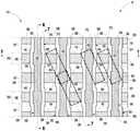
图1到7为根据本发明的一些实施例的过程中的DRAM构造的一部分的图解横截面图。1-7 are diagrammatic cross-sectional views of a portion of a DRAM construction in process according to some embodiments of the present invention.
图8到24为根据本发明的一些实施例的过程中的图1到7的构造的图解依序截面图。8-24 are diagrammatic sequential cross-sectional views of the constructions of FIGS. 1-7 in process according to some embodiments of the present invention.
具体实施方式Detailed ways
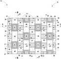
本发明的实施例涵盖集成电路构造,例如DRAM构造,以及用于形成集成电路构造,例如DRAM电路构造的方法。参考图1到7描述包括DRAM构造的第一实例实施例,图1到7展示包括已相对于基底衬底11制造的阵列或阵列区域10的衬底构造8的实例片段。衬底构造11可包括导电/导体/传导、半导电/半导体/半传导以及绝缘/绝缘体/隔绝(即,在本文中电气地)材料中的任何一个或多个。各种材料位于基底衬底11上方。材料可在图1到7所描绘材料的旁边、竖向向内或竖向向外。举例来说,集成电路的其它部分制造或完全制造的组件可设置在基底衬底11上方、周围或内部某处。还可制造用于操作存储器阵列内的组件的控制电路和/或其它外围电路,且所述电路可或可不完全或部分地在存储器阵列或子阵列内。此外,也可相对彼此独立地、先后地或以其它方式制造和操作多个子阵列。如此文件中所使用,“子阵列”也可被视为阵列。Embodiments of the invention encompass integrated circuit constructions, such as DRAM constructions, and methods for forming integrated circuit constructions, such as DRAM circuit constructions. A first example embodiment including a DRAM construction is described with reference to FIGS. 1-7 , which show an example fragment of a
基底衬底11包括半导电材料12(例如,适当地且不同地掺杂的单晶和/或多晶硅、Ge、SiGe、GaAs,和/或其它现有或未来研发的半导电材料)、沟槽隔离区14(例如,氮化硅和/或二氧化硅),以及包括合适地且不同地掺杂的半导电材料12的主动区域区16。在一个实施例中,构造8包括存储器单元75(图5和7,且为了在这些图中清楚起见,具有图5中展示的仅四个轮廓75和图7中的仅两个轮廓75),例如DRAM存储器单元,其个别地包括场效应晶体管装置25(图3)和存储元件(例如电容器85;图1和7)。然而,本发明的实施例涵盖独立于是否含有存储器单元的其它存储器单元和集成电路的其它构造。
实例晶体管装置25个别地包括一对源极/漏极区、在所述对的源极/漏极区之间的沟道区、以操作方式接近沟道区的导电栅极,以及在导电栅极与沟道区之间的栅极绝缘体。装置25被展示为凹陷的存取装置,其中实例构造8展示这些凹陷的存取装置在此类装置的个别对中分组。个别凹陷的存取装置25包含例如在半导电材料12中的沟槽19内的埋式存取线构造18。构造18包括充当个别装置25的导电栅极的导电栅极材料22(例如,导电掺杂的半导体材料和/或金属材料,包含例如元素W、Ru和/或Mo)。栅极绝缘体20(例如,二氧化硅和/或氮化硅)在导电栅极材料22与半导电材料12之间沿着个体沟槽19的侧壁21和基底23。绝缘体材料37(例如,二氧化硅和/或氮化硅)在材料20和22上方的沟槽19内。个别装置25包括在个别沟槽19的相对侧上的在半导电材料12的上部部分中的一对源极/漏极区24、26(例如,区24、26从存取线构造18横向地向外且高于所述存取线构造18)。源极/漏极区24、26中的每一个具有其至少一个部分,在所述至少一个部分中具有导电性增大的掺杂剂,所述掺杂剂是相应源极/漏极区24、26内的最大浓度的此类导电性增大的掺杂剂,例如以使得此部分是导电的(例如,具有至少1019原子/cm3的最大掺杂剂浓度)。因此,所有的或仅一部分的每一源极/漏极区24、26可具有此类最大浓度的导电性增大的掺杂剂。源极/漏极区24和/或26可包含其它掺杂区(未展示),例如卤素区、LDD区等。
在所述对凹陷的存取装置25的个别者中的所述对源极/漏极区的源极/漏极区中的一个(例如区26)横向地在导电栅极材料22之间且由所述对装置25共享。所述对源极/漏极区的其它源极/漏极区(例如区24)并不由所述对装置25共享。因此,在实例实施例中,每一主动区域区16包括两个装置25(例如一对装置25),其中每一装置共享中央源极/漏极区26。One of the source/drain regions of the pair of source/drain regions in an individual of the pair of recessed access devices 25 (eg, region 26 ) is laterally between
实例沟道区27(图1、3、6及7)在半导电材料12中沿着沟槽侧壁21(图6及7)在一对源极/漏极区24、26下方且围绕沟槽基底23。沟道区27可为未掺杂的或可合适地掺杂有导电性增大的掺杂剂,所述导电性增大的掺杂剂很可能是源极/漏极区24、26中的相反导电性类型的掺杂剂,且例如在沟道中具有不超过1x 1017原子/cm3的最大浓度。当合适的电压被施加到存取线构造18的栅极材料22时,导电沟道在沟道区27内接近栅极绝缘体20形成(例如,沿着沟道电流流动管线/路径29[图7]),使得电流能够在个别主动区域区16内在存取线构造18下在一对源极/漏极区24与26之间流动。以图解方式展示了点刻法以指示主要导电性修改的掺杂剂浓度(无论类型如何),其中较稠密点刻法指示较大掺杂剂浓度且较轻点刻法指示较低掺杂剂浓度。导电性修改的掺杂剂可以在且将很可能在如所展示的材料12的其它部分中。为方便起见,在材料12中仅展示了两个不同的点刻法密度,且可使用额外的掺杂剂浓度,并且在任何区中不需要恒定掺杂剂浓度。Example channel region 27 ( FIGS. 1 , 3 , 6 and 7 ) in
水平间隔开的导电通孔33个别地直接电耦合到多个晶体管的所述对源极/漏极区中的一个(例如26)。实例导电通孔33通过中间材料(例如,当存在时,为材料38、32和/或46中的一或多个,其中材料38、32和46如下文所描述)相对于彼此(例如,如下文所述,纵向相对于其上的数字线39)间隔开,且包括导电材料(例如34和35)。在一个实施例中,导电通孔33的导电材料34/35包括上部导电材料35(例如金属材料)下方的下部导电掺杂的半导电材料34(例如,导电掺杂的多晶硅),所述下部导电材料35具有与导电掺杂的半导电材料34的组成不同的组成。材料34和35的额外实例导电材料,且仅作为实例,包括金属氮化物(例如,TiN、TaN、WN、MoN)、金属碳氮化物(例如,TiCN、TaCN、WCN、MoCN)和元素形式金属(例如,Ti、Ta、W、Mo、Co、Cu、Ru、Be),包括其组合、化合物和合金。Horizontally spaced
数字线39沿多个晶体管25的线直接电耦合到多个导电通孔33。数字线39包括直接抵靠着导电通孔33的导电材料34/35的传导材料42。实例数字线39包括数字线结构30的部分,所述数字线结构30的部分包括相对纵向绝缘侧面38(例如,二氧化硅和/或氮化硅)和绝缘盖50(例如,氮化硅和/或二氧化硅)。实例材料46在数字线39下方在紧密地纵向邻近的导电通孔33(图6)之间。下部绝缘材料48(例如,二氧化硅、氮化硅、二氧化铝、氧化铪等中的一或多个;例如,50到200埃的厚度)在材料46下方在紧密地纵向邻近的导电通孔33之间。材料46可为绝缘的、半导电的(例如,不充分掺杂为导电的材料),或导电的或被消除,其中传导材料42向内延伸到下部绝缘材料48(未展示)。
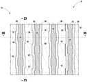
数字线结构30的个别者具有传导材料(例如42)的纵向交替的较宽区和较窄区(例如,分别为55和57)。较宽区55直接在个别导电通孔33的顶部表面(例如58)上方且直接抵靠着所述顶部表面,且在顶部表面58处的水平横截面(例如,图5的横截面)中相对于所述水平横截面中的较窄区57更宽,其中较窄区57纵向地在较宽区55之间。Individual ones of
在一个实施例中,个别数字线39具有直接在导电通孔33上方的相对于沿相应个别数字线39纵向地在其间的更低的底部表面60。在一个实施例中,个别数字线39具有波状顶部表面62(图1、6和7)。在一个此实施例中,波状顶部表面62的最高部分63直接在较窄区57上方,且在一个此实施例中,最高部分63不直接在较宽区55上方。In one embodiment, the
导体通孔36横向地在数字线结构30之间且纵向地沿数字线结构30间隔开。导体通孔36的个别直接电耦合到多个晶体管的所述对源极/漏极区中的另一源极/漏极区(例如24)。多个存储元件(例如电容器85)直接电耦合到个别导体通孔36。为方便和清楚起见,组件33、30、36等展示为具有竖直侧壁,但这样可向内或向外逐渐变窄,从而移动到所描绘堆叠(未展示)中。
如本文中关于其它实施例展示和/或描述的任何其它属性或方面可用于参考上文实施例展示和描述的实施例中。Any other attributes or aspects as shown and/or described herein with respect to other embodiments may be used in the embodiments shown and described with reference to the above embodiments.
本发明的实施例涵盖可为或可不为或包括存储器电路的集成电路。根据本发明的集成电路包括衬底(例如,导电通孔33下方的材料12和14的那些部分)上方的水平间隔开的导电通孔(例如33)。多个导电线(例如39)个别地直接在纵向地沿相应个别导电线间隔开的多个导电通孔上方。导电线的个别具有纵向交替的较宽区(例如55)和较窄区(例如,57)。较宽区直接在导电通孔的个别的顶部表面(例如58)上方且直接抵靠着所述顶部表面,且在顶部表面处的水平横截面(例如,图5的横截面)中相对于所述水平横截面中的较窄区更宽,其中较窄区纵向地在较宽区之间。可使用如本文中关于其它实施例所展示和/或描述的任何其它属性或方面。Embodiments of the invention encompass integrated circuits that may or may not be or include memory circuits. Integrated circuits in accordance with the present invention include horizontally spaced conductive vias (eg, 33 ) over a substrate (eg, those portions of
本发明的实施例涵盖用于形成集成电路构造,例如包括DRAM、其它存储器和/或非存储器电路的方法。无论如何,本发明的方法方面可使用或具有在结构和/或装置实施例中的如本文中所描述的属性中的任一个。同样地,上文所描述的结构实施例可并入相对于方法实施例方面描述的属性中的任一个。Embodiments of the invention encompass methods for forming integrated circuit constructs, eg, including DRAM, other memory, and/or non-memory circuits. Regardless, method aspects of the invention may use or have any of the properties as described herein in structural and/or device embodiments. Likewise, the structural embodiments described above may incorporate any of the attributes described in relation to the method embodiments.
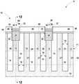
参考图8到24描述实例方法实施例和用于产生图1到7的构造8的实例此实施例。参考图8、9和10,这分别相对于图1、4和6的构造展示前趋构造,其中构造8已制造到包括阵列10内的材料32、34和35的点。开口56已形成到源极/漏极区26。此外,图8到10展示晶体管25的先前形成(在一个实施例中),所述晶体管25个别地包括一对源极/漏极区24、26,在一对源极/漏极区24、26之间的沟道区27,以及以操作方式接近沟道区27的导电栅极(例如导电材料22)。此外,且在一个实施例中,已形成水平间隔开的导电通孔33,其个别地直接电耦合到多个晶体管25的所述对源极/漏极区中的一个(例如,源极/漏极区26)。An example method embodiment and an example such embodiment for producing the
参考图11和12,导电通孔33已竖直地凹陷(例如,其导电材料35和通过化学刻蚀)以个别地具有低于横向包围材料(例如,32或46)的顶部表面的顶部表面58。Referring to Figures 11 and 12,
参考图13到15,已直接在竖直凹陷的导电通孔33上方且直接抵靠着所述导电通孔33形成传导材料42。传导材料42具有直接在竖直凹陷的导电通孔33上方相对于横向邻近的竖直凹陷的导电通孔33的较高顶部表面52更低的顶部表面51。已直接在传导材料42上方形成掩蔽材料50(例如,绝缘氮化硅或其它材料)。掩蔽材料50直接在较低顶部表面51上方相对于直接在与其横向邻近的较高顶部表面52上方(例如T2)竖直地更厚(例如T1)。可或可不至少部分地保持为完成电路构造的部分的掩蔽材料50可初始地沉积为不如此竖直地较厚和较薄,且可随后通过使掩蔽材料50经历平面化步骤(例如,机械抛光或化学机械抛光)来产生所描绘构造。Referring to FIGS. 13-15 ,
参考图16到19,已图案化掩蔽材料50和导电材料42(例如使用光刻图案化和使用掩蔽块59[例如光刻胶]的刻蚀)以形成个别导电线结构30,所述导电线结构30个别地直接在纵向地沿相应个别导电线结构30间隔开的多个竖直凹陷的导电通孔33上方。在一个实施例中,且由于或因为存在竖直较厚的掩蔽材料(例如T1)而产生的伪影,此情况形成个别导电线结构30以分别具有传导材料42的纵向交替的较宽区55和较窄区57。传导材料42的较宽区55直接在个别竖直凹陷的导电通孔33的较低顶部表面58上方且直接抵靠着所述较低顶部表面58,且在竖直凹陷的导电通孔的较低顶部表面58(例如,图18)处的水平横截面中相对于在所述水平横截面中的传导材料42的较窄区57更宽。传导材料42的较窄区57纵向地在传导材料42的较宽区55之间。图案化掩蔽材料50和传导材料42的此动作可在个别导电通孔33周围形成圆周空隙61。16-19, masking
参考图20到23,已形成绝缘间隔物38(因此,扩增数字线结构30的大小),且介电材料40已沉积在其间。如所展示,绝缘间隔物38可填充圆周空隙61。图24展示此处穿到源极/漏极区24的开口41的后续形成。将进行后续处理以产生如图1到7中所展示的构造。举例来说,将在开口41中形成导体通孔36以个别地直接电耦合到所述对源极/漏极区的其它源极/漏极区24。将形成存储元件,例如电容器85,以直接电耦合到导体通孔36的个别。20-23, insulating
可使用如本文中关于其它实施例所展示和/或描述的任何其它属性或方面。Any other attributes or aspects as shown and/or described herein with respect to other embodiments may be used.
本发明的实施例涵盖用于形成可为或可不为或包括存储器电路的集成电路的方法。此方法包括在衬底(例如,导电通孔33下方的材料12和14的那些部分)上方形成水平间隔开的导电通孔(例如,33)。直接在导电通孔上方且直接抵靠着导电通孔形成传导材料(例如42)。图案化传导材料(不论材料50的存在)以形成个别导电线(例如39),所述导电线个别地直接在纵向地沿相应个别导电线间隔开的多个导电通孔上方。所述图案化形成个别导电线以具有纵向交替的较宽区和较窄区(例如,分别为55、57)。较宽区直接在导电通孔的个别的顶部表面(例如58)上方且直接抵靠着所述顶部表面,且在顶部表面(例如图18的顶部表面)处的水平横截面中相对于所述水平横截面中的较窄区更宽。较窄区纵向地在较宽区之间。可使用如本文中关于其它实施例所展示和/或描述的任何其它属性或方面。Embodiments of the invention encompass methods for forming integrated circuits that may or may not be or include memory circuits. This method includes forming horizontally spaced conductive vias (eg, 33 ) over the substrate (eg, those portions of
上述处理或构造可被视为相对于组件的阵列,所述组件形成为此类组件的单个堆叠或单个叠组或在单个堆叠或单个叠组内,所述堆叠或叠组在底层基底衬底上方或作为底层基底衬底的部分(但单个堆叠/叠组可具有多个层)。用于操作或存取阵列内的此类组件的控制和/或其它外围电路作为完成构造的部分也可形成于任何位置,且在一些实施例中可以在阵列下面(例如,阵列下方的CMOS)。无论如何,一或多个额外此类堆叠/叠组可提供或制造于在图中所展示或上文所描述的堆叠/叠组上方和/或下方。此外,组件的阵列在不同堆叠/叠组中可相对彼此相同或不同,且不同堆叠/叠组可相对彼此具有相同厚度或不同厚度。居间结构可设置在紧密地竖直邻近的堆叠/叠组之间(例如,额外电路和/或介电层)。另外,不同堆叠/叠组可相对彼此电耦合。多个堆叠/叠组可单独地且依序地(例如,一个在另一个顶上)制造,或者两个或更多个堆叠/叠组可基本上同时制造。The above process or construction may be considered relative to an array of components formed as or within a single stack or stack of such components on an underlying base substrate over or as part of the underlying base substrate (although a single stack/stack may have multiple layers). Control and/or other peripheral circuits for operating or accessing such components within the array may also be formed anywhere as part of completing the construction, and in some embodiments may be beneath the array (eg, CMOS below the array) . Regardless, one or more additional such stacks/stacks may be provided or fabricated above and/or below the stacks/stacks shown in the figures or described above. Furthermore, the arrays of components may be the same or different relative to each other in different stacks/stacks, and the different stacks/stacks may have the same thickness or different thicknesses relative to each other. Intervening structures may be disposed between closely vertically adjacent stacks/stacks (eg, additional circuitry and/or dielectric layers). Additionally, different stacks/stacks may be electrically coupled relative to each other. Multiple stacks/stacks may be fabricated individually and sequentially (eg, one on top of the other), or two or more stacks/stacks may be fabricated substantially simultaneously.
上文所论述的组合件和结构可用于集成电路/电路系统中且可并入于电子系统中。此类电子系统可用于例如存储器模块、装置驱动器、功率模块、通信调制解调器、处理器模块和专用模块中,且可包含多层、多芯片模块。电子系统可以是以下广泛范围的系统中的任一个:例如摄像机、无线装置、显示器、芯片组、机顶盒、游戏、照明、交通工具、时钟、电视、蜂窝电话、个人计算机、汽车、工业控制系统、飞机等。The assemblies and structures discussed above can be used in integrated circuits/circuitry and can be incorporated into electronic systems. Such electronic systems may be used, for example, in memory modules, device drivers, power modules, communication modems, processor modules, and application-specific modules, and may include multi-layer, multi-chip modules. An electronic system can be any of a wide range of systems such as cameras, wireless devices, displays, chipsets, set-top boxes, games, lighting, vehicles, clocks, televisions, cellular phones, personal computers, automobiles, industrial control systems, airplane etc.
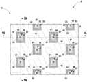
本文件中,除非另有指示,否则“竖向”、“较高”、“上部”、“较低”、“顶部”、“顶上”、“底部”、“上方”、“下方”、“在…下面”、“在…之下”、“向上”和“向下”通常参考竖直方向。“水平”是指沿着主衬底表面且可在制造期间相对于其处理衬底的大体方向(即,在10度内),且竖直是大体与其正交的方向。提及“恰好水平”是指沿着主衬底表面(即,与所述表面不形成度数)且可在制造期间相对于其处理衬底的方向。此外,如本文中所使用的“竖直”和“水平”是相对于彼此的大体上垂直方向,且独立于三维空间中衬底的定向。另外,“竖向延伸”和“竖向地延伸”是指从恰好水平倾斜至少45°的方向。此外,关于场效应晶体管“竖向地延伸”、“竖向延伸的”、“水平地延伸”、“水平延伸的”等是参考晶体管的沟道长度的定向,在操作中电流在源极/漏极区之间沿着所述定向流动。对于双极结晶体管,“竖向地延伸”、“竖向延伸的”、“水平地延伸”、“水平延伸的”等是参考基底长度的定向,在操作中电流在发射极与集电极之间沿着所述定向流动。在一些实施例中,竖向地延伸的任何组件、特征和/或区竖直地或在竖直的10°内延伸。In this document, unless otherwise indicated, the terms "vertical", "upper", "upper", "lower", "top", "above", "bottom", "above", "below", "Below", "under", "up" and "down" generally refer to the vertical direction. "Horizontal" refers to the general direction (ie, within 10 degrees) along the main substrate surface with respect to which the substrate can be handled during manufacture, and vertical is the direction generally orthogonal thereto. Reference to "exactly horizontal" refers to a direction along the main substrate surface (ie, not forming degrees from the surface) and relative to which the substrate can be handled during manufacture. Furthermore, "vertical" and "horizontal" as used herein are generally vertical directions relative to each other and are independent of the orientation of the substrate in three-dimensional space. Additionally, "extending vertically" and "extending vertically" refer to directions that are inclined at least 45° from exactly horizontal. Furthermore, references to field effect transistors "vertically extending", "vertically extending", "horizontal extending", "horizontal extending" etc. refer to the orientation of the channel length of the transistor, in operation the current is The flow between the drain regions follows the orientation. For bipolar junction transistors, "vertically extending", "vertically extending", "horizontal extending", "horizontal extending" etc. are orientations with reference to the length of the substrate, in operation current flows between the emitter and collector along the direction of flow. In some embodiments, any component, feature and/or region that extends vertically extends vertically or within 10° of vertical.
此外,“直接在…上方”、“直接在…下方”和“直接在…下面”要求两个所陈述区/材料/组件相对彼此的至少一些横向重叠(即,水平地)。另外,使用前面没有“直接”的“上方”仅要求在另一所陈述区/材料/组件上方的所陈述区/材料/组件的某一部分在另一所陈述区/材料/组件的竖向外侧(即,与两个所陈述区/材料/组件是否存在任何横向重叠无关)。类似地,使用前面没有“直接”的“下方”和“下面”仅要求在另一所陈述区域/材料/部件下方的所陈述区域/材料/部件的某一部分在另一所陈述区域/材料/部件的竖向内侧(即,与两个所陈述区域/材料/部件是否存在任何橫向重叠无关)。Furthermore, "directly above," "directly below," and "directly below" require at least some lateral overlap (ie, horizontally) of the two recited regions/materials/components relative to each other. Additionally, the use of "above" without "directly" before it only requires that some portion of a stated area/material/component that is above another stated area/material/component is vertically outside of another stated area/material/component (ie irrespective of whether there is any lateral overlap of the two stated regions/materials/components). Similarly, the use of "under" and "under" without "directly" before it only requires that a portion of a stated area/material/component that is below another stated area/material/component is in another stated area/material/ The vertical inner side of the component (ie irrespective of whether there is any lateral overlap of the two stated regions/materials/components).
本文中所描述的材料、区和结构中的任一个可为均匀的或非均匀的,且无论如何在其所覆的任何材料上方可为连续的或不连续的。当针对任何材料提供一或多种实例组合物时,所述材料可包括此一或多种组合物、主要由此一或多种组合物组成或由此一或多种组合物组成。此外,除非另行陈述,否则可使用任何合适的现有或未来开发的技术来形成每一材料,其中原子层沉积、化学气相沉积、物理气相沉积、外延生长、扩散掺杂和离子植入是实例。Any of the materials, regions, and structures described herein may be uniform or non-uniform, and in any event may be continuous or discontinuous over any material it overlies. When one or more example compositions are provided for any material, the material may include, consist essentially of, or consist of such one or more compositions. Furthermore, unless otherwise stated, each material may be formed using any suitable existing or future developed technique, of which atomic layer deposition, chemical vapor deposition, physical vapor deposition, epitaxial growth, diffusion doping, and ion implantation are examples .
另外,单独使用的“厚度”(前面无方向性形容词)被定义为从具有不同组成的紧邻材料或紧邻区的最接近表面垂直穿过给定材料或区的平均直线距离。另外,本文中所描述的各种材料或区可具有基本上恒定的厚度或具有可变的厚度。如果具有可变的厚度,那么除非另有指示,否则厚度是指平均厚度,且此类材料或区由于厚度可变而将具有某一最小厚度和某一最大厚度。如本文中所使用,“不同组成”仅要求两个所陈述材料或区的可直接抵靠彼此的那些部分在化学上和/或在物理上不同,例如在所述材料或区不均匀的情况下。如果两个所陈述材料或区彼此并未直接抵靠,那么在此类材料或区并不均匀的情况下,“不同组成”仅要求两个所陈述材料或区的彼此最接近的那些部分在化学上和/或在物理上不同。在此文档中,当所陈述材料、区或结构相对于彼此存在至少某一物理接触时,材料、区或结构“直接抵靠”另一材料、区或结构。相比之下,前面没有“直接”的“上方”、“在……上”、“邻近”、“沿着”和“抵靠”涵盖“直接抵靠”以及其中居间材料、区或结构使得所陈述的材料、区或结构相对彼此无物理触摸接触的构造。Additionally, "thickness" (preceded by non-directional adjective), used alone, is defined as the average straight-line distance perpendicular to a given material or region from the closest surface of immediately adjacent materials or regions of different composition. Additionally, the various materials or regions described herein can have a substantially constant thickness or have a variable thickness. If of variable thickness, unless otherwise indicated, the thickness refers to the average thickness, and such materials or regions will have a certain minimum thickness and a certain maximum thickness due to the variable thickness. As used herein, "different composition" requires only those portions of the two stated materials or regions that are chemically and/or physically different, such as where the materials or regions are not homogeneous, that may directly abut each other Down. If two recited materials or regions are not directly abutting each other, then where such materials or regions are not homogeneous, "different composition" requires only those parts of the two recited materials or regions that are closest to each other are in Chemically and/or physically different. In this document, a material, region or structure is "directly abutted" against another material, region or structure when the stated materials, regions or structures are in at least some physical contact with respect to each other. In contrast, "above," "on," "adjacent," "along," and "abut" without "directly" before cover "directly abut" and where intervening materials, regions, or structures are such that The stated materials, regions or structures have no physical touch contact configuration with respect to each other.
本文中,如果在正常操作中,电流能够从一个区-材料-组件连续流动到另一区-材料-组件,且在充足地产生亚原子正和/或负电荷时主要通过所述亚原子正和/或负电荷的移动来进行所述流动,则所述区-材料-组件相对于彼此“电耦合”。另一电子组件可在所述区-材料-组件之间且电耦合到所述区-材料-组件。相比之下,当区-材料-组件称为“直接电耦合”时,直接电耦合的区-材料-组件之间没有介入的电子组件(例如,没有二极管、晶体管、电阻器、换能器、交换器、熔断器等)。Herein, if in normal operation current can flow continuously from one region-material-component to another region-material-component, and mainly through the subatomic positive and/or negative subatomic charges when sufficient to generate positive and/or negative charges or movement of negative charge to effect the flow, the region-material-components are "electrically coupled" with respect to each other. Another electronic component can be between and electrically coupled to the region-material-component. In contrast, when a region-material-component is referred to as "direct electrical coupling", there are no intervening electronic components (eg, no diodes, transistors, resistors, transducers) between the directly electrically coupled region-material-components , switches, fuses, etc.).
此文件中的“行”和“列”的任何使用是为了方便区分一个系列或定向的特征与另一系列或定向的特征,且组件已或可沿着所述“行”和“列”形成。“行”及“列”关于任何系列的区、组件和/或特征同义地使用,与功能无关。无论如何,行可相对彼此笔直和/或弯曲和/或平行和/或不平行,列可同样如此。此外,行及列可相对彼此以90°或以一或多个其它角度(即,除平角之外)相交。Any use of "rows" and "columns" in this document is for convenience to distinguish one series or orientation of features from another series or orientation of features along which components have been or may be formed . "Row" and "column" are used synonymously with respect to any series of regions, components and/or features, regardless of function. In any event, the rows may be straight and/or curved and/or parallel and/or non-parallel relative to each other, as may the columns. Furthermore, the rows and columns may intersect at 90° relative to each other or at one or more other angles (ie, other than straight angles).
本文中的导电/导体/传导材料中的任一个的组成可为金属材料和/或导电掺杂的半导电/半导体/半传导材料。“金属材料”是元素金属、两种或更多种元素金属的任何混合物或合金和任何一或多种导电金属化合物中的任一种或组合。The composition of any of the conductive/conductor/conductive materials herein may be metallic materials and/or conductively doped semiconducting/semiconductor/semiconducting materials. A "metallic material" is any one or combination of an elemental metal, any mixture or alloy of two or more elemental metals, and any one or more conductive metal compounds.
本文中,关于刻蚀(etch)、刻蚀(etching)、移除(removing)、移除(removal)、沉积、形成(forming)和/或形成(formation)的“选择性”的任何使用是一种所陈述材料以按体积计至少2:1的速率相对于所作用的另一所陈述材料进行的这一动作。此外,对选择性地沉积、选择性地生长或选择性地形成的任何使用是以按体积计至少2:1的比率使一种材料相对于另一种或多种所陈述材料沉积、生长或形成达至少第一75埃的沉积、生长或形成。As used herein, any use of "selectivity" with respect to etching, etching, removing, removing, depositing, forming and/or formation is This action of one recited material relative to the other recited material being acted upon at a rate of at least 2:1 by volume. Furthermore, any use of selectively depositing, selectively growing or selectively forming is to deposit, grow or otherwise deposit one material relative to another recited material or materials in a ratio of at least 2:1 by volume. A deposition, growth or formation is formed up to at least a first 75 angstroms.
除非另有指示,否则本文中“或”的使用涵盖任一个和两者。The use of "or" herein encompasses either and both unless otherwise indicated.
结论in conclusion
在一些实施例中,一种用于形成集成电路的方法包括在衬底上方形成水平间隔开的导电通孔。直接在导电通孔上方且直接抵靠着导电通孔形成传导材料。图案化传导材料以形成个别导电线,所述个别导电线个别地直接在纵向地沿相应个别导电线间隔开的多个导电通孔上方。所述图案化形成个别导电线以具有纵向交替的较宽区和较窄区。较宽区直接在导电通孔的个别的顶部表面上方且直接抵靠着所述顶部表面,且在顶部表面处的水平横截面中相对于所述水平横截面中的较窄区更宽。较窄区纵向地在较宽区之间。In some embodiments, a method for forming an integrated circuit includes forming horizontally spaced conductive vias over a substrate. The conductive material is formed directly over and directly against the conductive via. The conductive material is patterned to form individual conductive lines that are individually directly over a plurality of conductive vias spaced longitudinally along the respective individual conductive lines. The patterning forms individual conductive lines to have longitudinally alternating wider and narrower regions. The wider regions are directly above and directly against the respective top surfaces of the conductive vias, and are wider in the horizontal cross-section at the top surfaces relative to the narrower regions in the horizontal cross-section. The narrower regions are longitudinally between the wider regions.
在一些实施例中,一种用于形成存储器电路的方法包括形成晶体管,所述晶体管个别地包括一对源极/漏极区、在所述对源极/漏极区之间的沟道区,以及以操作方式接近沟道区的导电栅极。形成水平间隔开的导电通孔,其个别地直接电耦合到多个晶体管的所述对源极/漏极区中的一个。使导电通孔竖直地凹陷以个别地具有低于横向包围材料的顶部表面的顶部表面。直接在竖直凹陷的导电通孔上方且直接抵靠着所述导电通孔形成传导材料。传导材料具有直接在竖直凹陷的导电通孔上方相对于横向邻近的竖直凹陷的导电通孔的较高顶部表面更低的顶部表面。直接在传导材料上方形成掩蔽材料。掩蔽材料直接在较低顶部表面上方相对于直接在与其横向邻近的较高顶部表面上方竖直地更厚。图案化掩蔽材料和传导材料以形成个别导电线结构,所述个别导电线结构个别地直接在纵向地沿相应个别导电线结构间隔开的多个竖直凹陷的导电通孔上方。竖直较厚的掩蔽材料形成个别导电线结构以具有传导材料的纵向交替的较宽区和较窄区。传导材料的较宽区直接在竖直凹陷的导电通孔的个别的较低顶部表面上方且直接抵靠着所述较低顶部表面,且在竖直凹陷的导电通孔的较低顶部表面处的水平横截面中相对于在所述水平横截面中的传导材料的较窄区更宽。传导材料的较窄区纵向地在传导材料的较宽区之间。导体通孔横向地在数字线结构之间形成且纵向地沿数字线结构间隔开。导电通孔的个别直接电耦合到多个晶体管的所述对源极/漏极区中的另一源极/漏极区。形成多个存储元件,其个别地直接电耦合到导体通孔的个别。In some embodiments, a method for forming a memory circuit includes forming transistors that individually include a pair of source/drain regions, a channel region between the pair of source/drain regions , and a conductive gate operatively close to the channel region. Horizontally spaced conductive vias are formed that are individually electrically coupled directly to one of the pair of source/drain regions of the plurality of transistors. The conductive vias are vertically recessed to individually have top surfaces lower than the top surfaces of the laterally surrounding material. Conductive material is formed directly over and directly against the vertically recessed conductive vias. The conductive material has a lower top surface directly above the vertically recessed conductive via relative to a higher top surface of a laterally adjacent vertically recessed conductive via. A masking material is formed directly over the conductive material. The masking material is vertically thicker directly above the lower top surface relative to directly above its laterally adjacent higher top surface. The masking material and the conductive material are patterned to form individual conductive line structures individually directly over a plurality of vertically recessed conductive vias spaced longitudinally along the respective individual conductive line structures. The vertically thicker masking material forms individual conductive line structures to have longitudinally alternating wider and narrower regions of conductive material. The wider regions of conductive material are directly above and directly against the respective lower top surfaces of the vertically recessed conductive vias, and at the lower top surfaces of the vertically recessed conductive vias The narrower region of the conductive material is wider in the horizontal cross-section than in the horizontal cross-section. The narrower regions of conductive material are longitudinally between the wider regions of conductive material. Conductor vias are formed laterally between the digit line structures and spaced longitudinally along the digit line structures. Individual ones of the conductive vias are directly electrically coupled to another source/drain region of the pair of source/drain regions of the plurality of transistors. A plurality of storage elements are formed that are individually electrically coupled directly to individual ones of the conductor vias.
在一些实施例中,集成电路包括衬底上方的水平间隔开的导电通孔。多个导电线个别地直接在纵向地沿相应个别导电线间隔开的多个导电通孔上方。导电线的个别具有纵向交替的较宽区和较窄区。较宽区直接在导电通孔的个别的顶部表面上方且直接抵靠着所述顶部表面,且在顶部表面处的水平横截面中相对于所述水平横截面中的较窄区更宽。较窄区纵向地在较宽区之间。In some embodiments, the integrated circuit includes horizontally spaced conductive vias over the substrate. The plurality of conductive lines are individually directly over the plurality of conductive vias spaced longitudinally along the respective individual conductive lines. Individual ones of the conductive lines have longitudinally alternating wider and narrower regions. The wider regions are directly above and directly against the respective top surfaces of the conductive vias, and are wider in the horizontal cross-section at the top surfaces relative to the narrower regions in the horizontal cross-section. The narrower regions are longitudinally between the wider regions.
在一些实施例中,存储器电路包括衬底,所述衬底包括晶体管,所述晶体管个别地包括一对源极/漏极区、在所述对源极/漏极区之间的沟道区,以及以操作方式接近沟道区的导电栅极。水平间隔开的导电通孔个别地直接电耦合到多个晶体管的所述对源极/漏极区中的一个。数字线结构沿多个晶体管的线个别地直接电耦合到多个导电通孔。数字线结构的个别具有传导材料的纵向交替的较宽区和较窄区。较宽区直接在导电通孔的个别的顶部表面上方且直接抵靠着所述顶部表面,且在顶部表面处的水平横截面中相对于所述水平横截面中的较窄区更宽。较窄区纵向地在较宽区之间。导体通孔横向地在数字线结构之间且纵向地沿数字线结构间隔开。导电通孔的个别直接电耦合到多个晶体管的所述对源极/漏极区中的另一源极/漏极区。多个存储元件个别地直接电耦合到导体通孔的个别。In some embodiments, a memory circuit includes a substrate including transistors, the transistors individually including a pair of source/drain regions, a channel region between the pair of source/drain regions , and a conductive gate operatively close to the channel region. The horizontally spaced conductive vias are individually electrically coupled directly to one of the pair of source/drain regions of the plurality of transistors. The digit line structures are individually directly electrically coupled to the plurality of conductive vias along the lines of the plurality of transistors. Individual ones of the digit line structures have longitudinally alternating wider and narrower regions of conductive material. The wider regions are directly above and directly against the respective top surfaces of the conductive vias, and are wider in the horizontal cross-section at the top surfaces relative to the narrower regions in the horizontal cross-section. The narrower regions are longitudinally between the wider regions. The conductor vias are spaced laterally between the digit line structures and longitudinally along the digit line structures. Individual ones of the conductive vias are directly electrically coupled to another source/drain region of the pair of source/drain regions of the plurality of transistors. The plurality of storage elements are individually electrically coupled directly to individual ones of the conductor vias.
根据规定,已就结构和方法特征而言以更具体或更不具体的语言描述了本文中所公开的主题。然而,应理解,权利要求书不限于所展示和描述的特定特征,因为本文中所公开的构件包括实例实施例。因此,权利要求书具有如书面所说明的整个范围,且应根据等效物原则恰当地进行解释。As required, the subject matter disclosed herein has been described in terms of structural and methodological features in more specific or less specific language. It is to be understood, however, that the claims are not limited to the specific features shown and described, as the components disclosed herein include example embodiments. Accordingly, the claims have the full scope as they are written and should be properly construed in accordance with the doctrine of equivalents.
Claims (29)
Applications Claiming Priority (2)
| Application Number | Priority Date | Filing Date | Title |
|---|---|---|---|
| US17/166,342 | 2021-02-03 | ||
| US17/166,342US11342336B1 (en) | 2021-02-03 | 2021-02-03 | Integrated circuitry, memory circuitry, method used in forming integrated circuitry, and method used in forming memory circuitry |
Publications (1)
| Publication Number | Publication Date |
|---|---|
| CN114863966Atrue CN114863966A (en) | 2022-08-05 |
Family
ID=81656513
Family Applications (1)
| Application Number | Title | Priority Date | Filing Date |
|---|---|---|---|
| CN202111313549.2APendingCN114863966A (en) | 2021-02-03 | 2021-11-08 | Integrated circuit, memory circuit, method for forming integrated circuit and method for forming memory circuit |
Country Status (2)
| Country | Link |
|---|---|
| US (2) | US11342336B1 (en) |
| CN (1) | CN114863966A (en) |
Families Citing this family (2)
| Publication number | Priority date | Publication date | Assignee | Title |
|---|---|---|---|---|
| US11785762B2 (en) | 2021-06-30 | 2023-10-10 | Micron Technology, Inc. | Memory circuitry and method used in forming memory circuitry |
| US12114489B2 (en)* | 2021-12-02 | 2024-10-08 | Micron Technology, Inc. | Vertical access line in a folded digitline sense amplifier |
Family Cites Families (2)
| Publication number | Priority date | Publication date | Assignee | Title |
|---|---|---|---|---|
| US8614151B2 (en)* | 2008-01-04 | 2013-12-24 | Micron Technology, Inc. | Method of etching a high aspect ratio contact |
| TWI560886B (en)* | 2014-09-25 | 2016-12-01 | Inotera Memories Inc | Non-floating vertical transistor structure and method for forming the same |
- 2021
- 2021-02-03USUS17/166,342patent/US11342336B1/enactiveActive
- 2021-11-08CNCN202111313549.2Apatent/CN114863966A/enactivePending
- 2022
- 2022-04-21USUS17/726,266patent/US12052857B2/enactiveActive
Also Published As
| Publication number | Publication date |
|---|---|
| US12052857B2 (en) | 2024-07-30 |
| US11342336B1 (en) | 2022-05-24 |
| US20220246622A1 (en) | 2022-08-04 |
Similar Documents
| Publication | Publication Date | Title |
|---|---|---|
| US11877438B2 (en) | Array of memory cells | |
| US11764234B2 (en) | Array of capacitors, an array of memory cells, method used in forming an array of memory cells, methods used in forming an array of capacitors, and methods used in forming a plurality of horizontally-spaced conductive lines | |
| US11659716B2 (en) | Memory circuitry and methods of forming memory circuitry | |
| US11925031B2 (en) | Arrays of capacitors and arrays of memory cells | |
| CN113380805A (en) | Integrated circuit, DRAM circuit and method for forming the same | |
| US10770465B1 (en) | Method used in forming integrated circuitry | |
| US20200006472A1 (en) | Elevationally-Elongated Conductive Structure Of Integrated Circuitry, Method Of Forming An Array Of Capacitors, Method Of Forming DRAM Circuitry, And Method Of Forming An Elevationally-Elongated Conductive Structure Of Integrated Circuitry | |
| US11411008B2 (en) | Integrated circuity, dram circuitry, methods used in forming integrated circuitry, and methods used in forming DRAM circuitry | |
| US12052857B2 (en) | Integrated circuitry, memory circuitry, method used in forming integrated circuitry, and method used in forming memory circuitry | |
| US10607998B1 (en) | Integrated circuitry, DRAM circuitry, method of forming a plurality of conductive vias, and method of forming DRAM circuitry | |
| US20220102348A1 (en) | Integrated Circuitry, Memory Circuitry, Method Used In Forming Integrated Circuitry, And Method Used In Forming Memory Circuitry | |
| US12363888B2 (en) | Memory circuitry and method used in forming memory circuitry | |
| CN112106197A (en) | Integrated circuit system architecture, DRAM architecture and method for forming integrated circuit system architecture | |
| US11469158B2 (en) | Construction of integrated circuitry and a method of forming an elevationally-elongated conductive via to a diffusion region in semiconductive material | |
| US20240224505A1 (en) | Memory Circuitry And Methods Used In Forming Memory Circuitry | |
| US20240260251A1 (en) | Memory Circuitry And Methods Used In Forming Memory Circuitry | |
| US20240172412A1 (en) | Memory Circuitry And Methods Used In Forming Memory Circuitry | |
| US20250261366A1 (en) | Memory Circuitry And Methods Used In Forming Memory Circuitry | |
| US20240274526A1 (en) | Memory Circuitry And Methods Used In Forming Memory Circuitry |
Legal Events
| Date | Code | Title | Description |
|---|---|---|---|
| PB01 | Publication | ||
| PB01 | Publication | ||
| SE01 | Entry into force of request for substantive examination | ||
| SE01 | Entry into force of request for substantive examination |