CN114859607A - Superlens, manufacturing method thereof and display device - Google Patents
Superlens, manufacturing method thereof and display deviceDownload PDFInfo
- Publication number
- CN114859607A CN114859607ACN202210442747.7ACN202210442747ACN114859607ACN 114859607 ACN114859607 ACN 114859607ACN 202210442747 ACN202210442747 ACN 202210442747ACN 114859607 ACN114859607 ACN 114859607A
- Authority
- CN
- China
- Prior art keywords
- substrate
- electrode layer
- liquid crystal
- dielectric
- superlens
- Prior art date
- Legal status (The legal status is an assumption and is not a legal conclusion. Google has not performed a legal analysis and makes no representation as to the accuracy of the status listed.)
- Pending
Links
Images


Classifications
- G—PHYSICS
- G02—OPTICS
- G02F—OPTICAL DEVICES OR ARRANGEMENTS FOR THE CONTROL OF LIGHT BY MODIFICATION OF THE OPTICAL PROPERTIES OF THE MEDIA OF THE ELEMENTS INVOLVED THEREIN; NON-LINEAR OPTICS; FREQUENCY-CHANGING OF LIGHT; OPTICAL LOGIC ELEMENTS; OPTICAL ANALOGUE/DIGITAL CONVERTERS
- G02F1/00—Devices or arrangements for the control of the intensity, colour, phase, polarisation or direction of light arriving from an independent light source, e.g. switching, gating or modulating; Non-linear optics
- G02F1/01—Devices or arrangements for the control of the intensity, colour, phase, polarisation or direction of light arriving from an independent light source, e.g. switching, gating or modulating; Non-linear optics for the control of the intensity, phase, polarisation or colour
- G02F1/13—Devices or arrangements for the control of the intensity, colour, phase, polarisation or direction of light arriving from an independent light source, e.g. switching, gating or modulating; Non-linear optics for the control of the intensity, phase, polarisation or colour based on liquid crystals, e.g. single liquid crystal display cells
- G02F1/133—Constructional arrangements; Operation of liquid crystal cells; Circuit arrangements
- G02F1/1333—Constructional arrangements; Manufacturing methods
- G02F1/1339—Gaskets; Spacers; Sealing of cells
- G02F1/13394—Gaskets; Spacers; Sealing of cells spacers regularly patterned on the cell subtrate, e.g. walls, pillars
- G—PHYSICS
- G02—OPTICS
- G02B—OPTICAL ELEMENTS, SYSTEMS OR APPARATUS
- G02B3/00—Simple or compound lenses
- G02B3/12—Fluid-filled or evacuated lenses
- G—PHYSICS
- G02—OPTICS
- G02F—OPTICAL DEVICES OR ARRANGEMENTS FOR THE CONTROL OF LIGHT BY MODIFICATION OF THE OPTICAL PROPERTIES OF THE MEDIA OF THE ELEMENTS INVOLVED THEREIN; NON-LINEAR OPTICS; FREQUENCY-CHANGING OF LIGHT; OPTICAL LOGIC ELEMENTS; OPTICAL ANALOGUE/DIGITAL CONVERTERS
- G02F1/00—Devices or arrangements for the control of the intensity, colour, phase, polarisation or direction of light arriving from an independent light source, e.g. switching, gating or modulating; Non-linear optics
- G02F1/01—Devices or arrangements for the control of the intensity, colour, phase, polarisation or direction of light arriving from an independent light source, e.g. switching, gating or modulating; Non-linear optics for the control of the intensity, phase, polarisation or colour
- G02F1/13—Devices or arrangements for the control of the intensity, colour, phase, polarisation or direction of light arriving from an independent light source, e.g. switching, gating or modulating; Non-linear optics for the control of the intensity, phase, polarisation or colour based on liquid crystals, e.g. single liquid crystal display cells
- G02F1/133—Constructional arrangements; Operation of liquid crystal cells; Circuit arrangements
- G02F1/1333—Constructional arrangements; Manufacturing methods
- G02F1/1339—Gaskets; Spacers; Sealing of cells
- G02F1/13396—Spacers having different sizes
- G—PHYSICS
- G02—OPTICS
- G02F—OPTICAL DEVICES OR ARRANGEMENTS FOR THE CONTROL OF LIGHT BY MODIFICATION OF THE OPTICAL PROPERTIES OF THE MEDIA OF THE ELEMENTS INVOLVED THEREIN; NON-LINEAR OPTICS; FREQUENCY-CHANGING OF LIGHT; OPTICAL LOGIC ELEMENTS; OPTICAL ANALOGUE/DIGITAL CONVERTERS
- G02F1/00—Devices or arrangements for the control of the intensity, colour, phase, polarisation or direction of light arriving from an independent light source, e.g. switching, gating or modulating; Non-linear optics
- G02F1/01—Devices or arrangements for the control of the intensity, colour, phase, polarisation or direction of light arriving from an independent light source, e.g. switching, gating or modulating; Non-linear optics for the control of the intensity, phase, polarisation or colour
- G02F1/13—Devices or arrangements for the control of the intensity, colour, phase, polarisation or direction of light arriving from an independent light source, e.g. switching, gating or modulating; Non-linear optics for the control of the intensity, phase, polarisation or colour based on liquid crystals, e.g. single liquid crystal display cells
- G02F1/133—Constructional arrangements; Operation of liquid crystal cells; Circuit arrangements
- G02F1/1333—Constructional arrangements; Manufacturing methods
- G02F1/1339—Gaskets; Spacers; Sealing of cells
- G02F1/13398—Spacer materials; Spacer properties
Landscapes
- Physics & Mathematics (AREA)
- Nonlinear Science (AREA)
- General Physics & Mathematics (AREA)
- Optics & Photonics (AREA)
- Mathematical Physics (AREA)
- Chemical & Material Sciences (AREA)
- Crystallography & Structural Chemistry (AREA)
- Devices For Indicating Variable Information By Combining Individual Elements (AREA)
- Liquid Crystal (AREA)
Abstract
Description
Translated fromChinese技术领域technical field
本发明涉及显示技术领域,具体的,涉及超透镜及其制作方法和显示装置。The present invention relates to the field of display technology, in particular, to a superlens, a method for making the same, and a display device.
背景技术Background technique
自由空间体显示,或在空间中创建发光图像点,这些显示技术可在稀薄的空气中成像,且在任意角度可视无裁切现象。因为边缘界限,“剪切现象”(通过人眼在不同的角度观察所显示的图像会存在差别,人眼并不能够在各个角度都观察到完整的图像,“剪切现象”即是指的人眼不能够观察到完整的图像的情况)限制了所有在二维表面对光进行调制的3D显示技术的应用,如全息显示、纳米光子阵列、等离子体显示等显示技术。虽然,目前的光泳体显示能够实现真三维显示的效果,但是整体器件体积相对较大。因此,目前亟需对现有的显示技术进行改进,以使器件能够实现空间体显示的基础上,进一步减小器件的体积,实现器件的集成化与小型化。Free-space volume displays, or the creation of glowing image points in space, these display technologies can be imaged in thin air and can be viewed from any angle without clipping. Because of edge boundaries, the "clipping phenomenon" (the displayed image will be different when viewed by the human eye at different angles, and the human eye cannot observe the complete image at all angles, and the "clipping phenomenon" refers to The fact that the human eye cannot observe a complete image) limits the application of all 3D display technologies that modulate light on two-dimensional surfaces, such as holographic displays, nanophotonic arrays, and plasmonic displays. Although the current photophoretic display can achieve the effect of true three-dimensional display, the overall device volume is relatively large. Therefore, there is an urgent need to improve the existing display technology so as to further reduce the volume of the device and realize the integration and miniaturization of the device on the basis of enabling the device to realize spatial volume display.
发明内容SUMMARY OF THE INVENTION
本发明是基于发明人对以下事实和问题的发现和认识做出的:The present invention is made based on the inventors' findings and understanding of the following facts and problems:
美国光学学会的显示技术组将“体积显示”定义为体积显示器的图像点与光散射(或吸收和生成)表面位于同一位置。目前,仅有感应等离子显示、改进空气显示、声悬浮显示在空间中被成功实现,但等离子显示未能展示RGB颜色;改进空气显示和声悬浮显示的机制太粗糙,与全息显示无法竞争。目前的光泳体显示能够实现真三维显示的效果,但是整体器件体积相对较大。发明人发现,可以利用液晶与介质柱形成超表面超表面结构以实现动态波束调控和聚焦功能,结合光泳力对纤维素粒子进行捕获以实现空间显示。The Optical Society's Display Technologies Group defines a "volume display" as a volume display where the image points are co-located with a light scattering (or absorbing and generating) surface. At present, only induction plasma display, improved air display, and acoustic levitation display have been successfully realized in space, but plasma display failed to display RGB colors; the mechanism of improved air display and acoustic levitation display is too rough to compete with holographic display. The current photophoretic display can achieve the effect of true three-dimensional display, but the overall device volume is relatively large. The inventors found that a metasurface metasurface structure can be formed by using liquid crystals and dielectric columns to achieve dynamic beam control and focusing functions, and cellulose particles can be captured in combination with photophoretic force to realize spatial display.
为了在至少在一定程度上解决相关技术中的技术问题之一,在本发明的一个方面,本发明提出了一种超透镜,所述超透镜包括:第一基板;第一电极层,所述第一电极层设置在所述第一基板的一侧;多个介质柱,多个所述介质柱间隔设置在所述第一电极层远离所述第一基板的一侧,在沿所述第一基板的中心向所述第一基板的边缘的延伸方向上,所述介质柱的宽度逐渐减小;第二电极层,所述第二电极层设置在所述介质柱远离所述第一基板的一侧;第一液晶,所述第一液晶位于所述第一电极层远离所述第一基板的一侧,且填充在多个所述介质柱之间的间隙中;第二基板,所述第二基板设置在所述第二电极层远离所述第一基板的一侧。由此,超透镜可以实现对动态波束的调控,并且可以实现聚焦,结合光泳力即可对纤维素粒子进行捕获,结合激光控制系统即可实现空间显示。In order to solve one of the technical problems in the related art at least to a certain extent, in one aspect of the present invention, the present invention provides a superlens, the superlens comprises: a first substrate; a first electrode layer, the The first electrode layer is arranged on one side of the first substrate; a plurality of dielectric pillars are arranged at intervals on the side of the first electrode layer away from the first substrate, along the first substrate. In the extending direction from the center of a substrate to the edge of the first substrate, the width of the dielectric column gradually decreases; the second electrode layer, the second electrode layer is disposed when the dielectric column is far from the first substrate one side; the first liquid crystal, the first liquid crystal is located on the side of the first electrode layer away from the first substrate, and is filled in the gaps between the plurality of the dielectric columns; the second substrate, the The second substrate is disposed on a side of the second electrode layer away from the first substrate. In this way, the metalens can realize the regulation of dynamic beams, and can realize focusing, cellulose particles can be captured in combination with photophoresis, and spatial display can be realized in combination with the laser control system.
根据本发明的实施例,所述超透镜进一步包括:第一配向膜,所述第一配向膜设置在所述第一液晶和所述第二电极层之间。由此,设置第一配向膜有利于提高超透镜的性能。According to an embodiment of the present invention, the metalens further includes: a first alignment film, the first alignment film being disposed between the first liquid crystal and the second electrode layer. Therefore, the provision of the first alignment film is beneficial to improve the performance of the superlens.
根据本发明的实施例,所述超透镜进一步包括:第三电极层,所述第三电极层设置在所述第二电极层和所述第一液晶之间;第二液晶,所述第二液晶位于所述第二电极层和所述第三电极层之间。由此,可以更好的实现超透镜对光束的调控和聚焦,更有利于实现空间显示。According to an embodiment of the present invention, the metalens further comprises: a third electrode layer, the third electrode layer is disposed between the second electrode layer and the first liquid crystal; a second liquid crystal, the second Liquid crystal is located between the second electrode layer and the third electrode layer. As a result, the control and focusing of the light beam by the superlens can be better achieved, which is more conducive to the realization of spatial display.
根据本发明的实施例,所述超透镜进一步包括:第二配向膜,所述第二配向膜设置在所述第一液晶和所述第三电极层之间。由此,设置第二配向膜可以使得超透镜具有更好的整体稳定性。According to an embodiment of the present invention, the superlens further includes: a second alignment film disposed between the first liquid crystal and the third electrode layer. Therefore, disposing the second alignment film can make the metalens have better overall stability.
根据本发明的实施例,所述超透镜进一步包括多个间隔设置的隔离柱,所述隔离柱设置所述第二电极层和所述第三电极层之间。由此,隔离柱可以起到良好的支撑作用,并且还能够使的第二液晶具有更好的稳定性。According to an embodiment of the present invention, the metalens further includes a plurality of spaced apart columns, the separation columns are arranged between the second electrode layer and the third electrode layer. Therefore, the spacer can play a good supporting role, and can also make the second liquid crystal have better stability.
根据本发明的实施例,所述介质柱满足以下条件的至少之一:所述介质柱的宽度为50nm~200nm;所述介质柱的高度为450nm~800nm;所述介质柱的材质包括氮化硅、氧化钛和氮化镓中的至少之一。由此,有利于进一步提高超透镜的性能。According to an embodiment of the present invention, the dielectric column satisfies at least one of the following conditions: the width of the dielectric column is 50 nm to 200 nm; the height of the dielectric column is 450 nm to 800 nm; the material of the dielectric column includes nitride At least one of silicon, titanium oxide and gallium nitride. Therefore, it is beneficial to further improve the performance of the metalens.
在本发明的另一方面,本发明提出了一种制作超透镜的方法,根据本发明的实施例,制作超透镜的方法包括:提供第一基板,并在所述第一基板的一侧形成第一电极层;在第一电极层远离所述第一基板的一侧形成多个间隔设置的介质柱,在沿所述第一基板的中心向所述第一基板的边缘的延伸方向上,所述介质柱的宽度逐渐减小;提供第二基板,并在所述第二基板的一侧形成第二电极层;将所述第一基板和所述第二基板对盒,使所述第一电极层位于所述第一基板和所述第二电极层之间,且所述第二电极层位于所述第二基板靠近所述第一基板的一侧;在所述第一电极层和所述第二电极层之间注入第一液晶,并使所述第一液晶填充在多个所述介质柱之间的间隙中。由此,利用上述方法制备得到的超透镜可以对动态波束进行良好的调控,并能够实现聚焦,还可以结合光泳力对纤维素粒子进行捕获,进一步的,将利用该方法制作得到的超透镜与激光控制系统结合可以实现空间显示;利用该方法制作超透镜有利于提高产品的良率。In another aspect of the present invention, the present invention provides a method for fabricating a superlens. According to an embodiment of the present invention, the method for fabricating a superlens includes: providing a first substrate, and forming on one side of the first substrate a first electrode layer; a plurality of dielectric columns arranged at intervals are formed on the side of the first electrode layer away from the first substrate, and in the extending direction from the center of the first substrate to the edge of the first substrate, The width of the dielectric column is gradually reduced; a second substrate is provided, and a second electrode layer is formed on one side of the second substrate; An electrode layer is located between the first substrate and the second electrode layer, and the second electrode layer is located on the side of the second substrate close to the first substrate; between the first electrode layer and the second electrode layer The first liquid crystal is injected between the second electrode layers, and the first liquid crystal is filled in the gaps between the plurality of the dielectric columns. Therefore, the metalens prepared by the above method can control the dynamic beam well, realize focusing, and can also capture the cellulose particles in combination with the photophoresis force. The combination of laser control system can realize spatial display; using this method to manufacture superlenses is beneficial to improve the yield of products.
根据本发明的实施例,在将所述第一基板和所述第二基板对盒之前,制作超透镜的方法进一步包括:在所述第二电极层远离所述第二基板的一侧形成第一配向膜。由此,可以通过设置第一配向膜提高超透镜的结构稳定性。According to an embodiment of the present invention, before assembling the first substrate and the second substrate, the method for fabricating a superlens further includes: forming a second electrode layer on a side of the second electrode layer away from the second substrate. an alignment film. Therefore, the structural stability of the metalens can be improved by providing the first alignment film.
根据本发明的实施例,制作超透镜的方法进一步包括:提供第三基板,并在所述第三基板的一侧形成第三电极层;将设置有所述第三电极层的所述第三基板与设置有所述介质柱的所述第一基板进行对盒;对所述第三基板进行刻蚀以除去所述第三基板;将设置有所述第二电极层的所述第二基板与设置有所述第三电极层的所述第一基板进行对盒;在所述第二电极层和所述第三电极层之间注入第二液晶。由此,设置第二液晶可以更好的实现超透镜对光束的调控。According to an embodiment of the present invention, the method for fabricating a superlens further includes: providing a third substrate, and forming a third electrode layer on one side of the third substrate; The substrate is boxed with the first substrate provided with the dielectric column; the third substrate is etched to remove the third substrate; the second substrate provided with the second electrode layer is performing cell assembling with the first substrate provided with the third electrode layer; and injecting a second liquid crystal between the second electrode layer and the third electrode layer. Therefore, setting the second liquid crystal can better realize the control of the light beam by the superlens.
根据本发明的实施例,在将所述第一基板和所述第三基板对盒之前,进一步包括:在所述第三电极层远离所述第三基板的一侧形成第二配向膜。由此,设置第二配向膜可以使得超透镜具有更好的结构稳定性。According to an embodiment of the present invention, before assembling the first substrate and the third substrate, the method further includes: forming a second alignment film on a side of the third electrode layer away from the third substrate. Therefore, disposing the second alignment film can make the metalens have better structural stability.
根据本发明的实施例,在将设置有所述第二电极层的所述第二基板与设置有所述第三电极层的所述第一基板进行对盒之前,制作超透镜的方法进一步包括:在所述第二电极层远离所述第二基板的一侧形成多个间隔设置的隔离柱。由此,可以进一步提高超透镜的结构稳定性。According to an embodiment of the present invention, before assembling the second substrate provided with the second electrode layer and the first substrate provided with the third electrode layer, the method for fabricating a superlens further includes : forming a plurality of spaced apart columns on the side of the second electrode layer away from the second substrate. Thereby, the structural stability of the metalens can be further improved.
在本发明的又一方面,本发明提出了一种显示装置,所述显示装置包括前面所述的超透镜或利用前面所述的方法制作的超透镜,由此,该显示装置具有前面所述的超透镜的全部特征以及优点,在此不再赘述。总的来说,该显示装置能够对光束进行良好的调控和聚焦。In yet another aspect of the present invention, the present invention provides a display device, the display device includes the aforementioned superlens or a superlens fabricated by the aforementioned method, whereby the display device has the aforementioned superlens All the features and advantages of the superlens will not be repeated here. In general, the display device can control and focus the light beam well.
根据本发明的实施例,所述显示装置进一步包括激光控制系统,所述激光控制系统与所述超透镜结合,进行实时位置信息和激光信息的同步。由此,该显示装置可以实现空间显示。According to an embodiment of the present invention, the display device further includes a laser control system, which is combined with the metalens to synchronize real-time position information and laser information. Thus, the display device can realize spatial display.
附图说明Description of drawings
图1显示了根据本发明一个实施例的超透镜的结构示意图;FIG. 1 shows a schematic structural diagram of a superlens according to an embodiment of the present invention;
图2显示了根据本发明另一个实施例的超透镜的结构示意图;FIG. 2 shows a schematic structural diagram of a superlens according to another embodiment of the present invention;
图3显示了根据本发明又一个实施例的超透镜的结构示意图;FIG. 3 shows a schematic structural diagram of a superlens according to yet another embodiment of the present invention;
图4显示了根据本发明又一个实施例的超透镜的结构示意图;FIG. 4 shows a schematic structural diagram of a superlens according to yet another embodiment of the present invention;
图5显示了根据本发明又一个实施例的超透镜的结构示意图;FIG. 5 shows a schematic structural diagram of a superlens according to yet another embodiment of the present invention;
图6显示了根据本发明又一个实施例的超透镜的结构示意图;6 shows a schematic structural diagram of a superlens according to yet another embodiment of the present invention;
图7显示了根据本发明一个实施例的超透镜沿BB’的截面图;Figure 7 shows a cross-sectional view of a metalens along BB' according to one embodiment of the present invention;
图8显示了本发明一个实施例中相位随介质柱直径变化的曲线图;Fig. 8 shows the graph of the phase change with the diameter of the dielectric column in one embodiment of the present invention;
图9显示了本发明一个实施例中光线透过率随介质柱直径变化的曲线图;FIG. 9 shows a graph of light transmittance as a function of the diameter of a dielectric column in an embodiment of the present invention;
图10显示了本发明一个实施例中相位随折射率变化的曲线图;Figure 10 shows a graph of phase versus refractive index in one embodiment of the present invention;
图11显示了一束光线经过本发明实施例的一个超透镜之后的波前的示意图;11 shows a schematic diagram of the wavefront of a beam of light after passing through a metalens according to an embodiment of the present invention;
图12显示了根据本发明一个实施例制作超透镜的方法流程图;Figure 12 shows a flow chart of a method for fabricating a superlens according to an embodiment of the present invention;
图13显示了根据本发明另一个实施例制作超透镜的方法流程图;Figure 13 shows a flowchart of a method for fabricating a superlens according to another embodiment of the present invention;
图14显示了根据本发明又一个实施例制作超透镜的方法流程图;Figure 14 shows a flow chart of a method for fabricating a superlens according to yet another embodiment of the present invention;
图15显示了根据本发明又一个实施例制作超透镜的方法流程图;Figure 15 shows a flowchart of a method for fabricating a superlens according to yet another embodiment of the present invention;
图16显示了根据本发明又一个实施例制作超透镜的方法流程图;Figure 16 shows a flowchart of a method for fabricating a superlens according to yet another embodiment of the present invention;
图17显示了根据本发明又一个实施例制作超透镜的方法流程图;Figure 17 shows a flow chart of a method for fabricating a superlens according to yet another embodiment of the present invention;
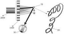
图18显示了纤维素粒子捕获以及动态图案显示的示意图;Figure 18 shows a schematic diagram of cellulose particle capture and dynamic pattern display;
图19显示了波束偏转示意图;Figure 19 shows a schematic diagram of beam steering;
图20显示了焦距随波前移动的示意图。Figure 20 shows a schematic diagram of the focal length moving with the wavefront.
附图标记说明:Description of reference numbers:
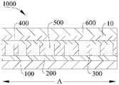
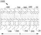
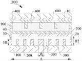
100:第一基板;200:第一电极层;300:介质柱;400:第二电极层;500:第一液晶;600:第二基板;700:第三电极层;800:第二液晶;900:隔离柱;10:第一配向膜;20:第二配向膜;30:第一封框胶;40:第二封框胶;50:第三基板;60:入射光束;70:纤维素粒子;80:图案;90:人眼。100: first substrate; 200: first electrode layer; 300: dielectric column; 400: second electrode layer; 500: first liquid crystal; 600: second substrate; 700: third electrode layer; 800: second liquid crystal; 900: spacer; 10: first alignment film; 20: second alignment film; 30: first sealant; 40: second sealant; 50: third substrate; 60: incident beam; 70: cellulose particle; 80: pattern; 90: human eye.
具体实施方式Detailed ways
下面详细描述本发明的实施例。下面描述的实施例是示例性的,仅用于解释本发明,而不能理解为对本发明的限制。实施例中未注明具体技术或条件的,按照本领域内的文献所描述的技术或条件或者按照产品说明书进行。Embodiments of the present invention are described in detail below. The embodiments described below are exemplary, only for explaining the present invention, and should not be construed as limiting the present invention. If no specific technique or condition is indicated in the examples, the technique or condition described in the literature in the field or the product specification is used.
在本发明的一方面,本发明提出了一种超透镜,根据本发明的实施例,参考图1至图6,超透镜1000包括第一基板100、第一电极层200、多个介质柱300、第二电极层400、第一液晶500和第二基板600,其中,第一电极层200设置在第一基板100的一侧,多个介质柱300间隔设置在第一电极层200远离第一基板100的一侧,在沿第一基板100的中心向第一基板100的边缘的延伸方向上(相当于沿图1至图6中A向水平方向箭头所示的方向上),介质柱的宽度W逐渐减小,第二电极层400设置在介质柱300远离第一基板100的一侧,第一液晶500位于第一电极层200远离第一基板100的一侧,且填充在多个介质柱300之间的间隙中,第二基板600设置在第二电极层400远离第一基板100的一侧。由此,该超透镜可以实现对动态波束的调控,还可以实现聚焦,结合光泳力即可实现捕获纤维素粒子的功能,将该超透镜与激光控制系统结合即可实现空间显示。In one aspect of the present invention, the present invention provides a superlens. According to an embodiment of the present invention, referring to FIGS. 1 to 6 , the
下面对本发明的超透镜可以实现对动态波束的调控和聚焦的原理进行说明:本发明中设置介质柱300的宽度W在沿第一基板100的中心向第一基板100的边缘的延伸方向上逐渐减小,图8示出了相位随介质柱直径变化的曲线图,图8中以介质柱为圆柱体为例示出了固定波长的光束在通过不同直径的介质柱之后的相位,由图8可知,介质柱直径越大,光束通过介质柱后的相位越大,相位延迟越大,光束(可参考图11)照射到超透镜300之后,由于中心位置的介质柱的宽度较大,光束移动较慢,而边缘位置的介质柱的宽度较小,光束移动较快,在沿中心向边缘延伸的方向上,光束移动速度逐渐增大,则可以形成类似图11中的抛物线形状的光波前L1,即可实现光束聚焦,而通过调节第一液晶500两端的电压则可以相应调节第一液晶500的晶轴方向,进而调节第一液晶500的折射率,相应的可以实现超透镜整体对动态光束的调控,使光波前位置发生变化,则动态波束经过超透镜之后的焦点会相应发生变化。第一液晶和介质柱可以对入射光束在x-y平面内的运动进行调控,也可以对入射光束在z方向(即垂直于x-y平面的方向)的运动进行调控,需要说明的是,第一液晶和介质柱不能同时调控x-y平面和z方向上的运动,由此,可以通过该超透镜对入射光束进行三维空间上的调控。The principle that the superlens of the present invention can realize the regulation and focusing of the dynamic beam will be described below: In the present invention, the width W of the
图9示出了介质柱为圆柱状,介质柱的材质为二氧化钛,高度为600nm,第一液晶为E7(折射率为1.5~1.7),在未施加电压的情况下(第一液晶的折射率保持1.5),介质柱的入射光为固定波长可见光的条件下,光线的透过率随介质柱的直径变化的曲线图,由图9可知当介质柱的直径设置在50nm~200nm的范围内时,光线的透过率均高于80%。Figure 9 shows that the dielectric column is cylindrical, the material of the dielectric column is titanium dioxide, the height is 600nm, the first liquid crystal is E7 (the refractive index is 1.5-1.7), and when no voltage is applied (the refractive index of the first liquid crystal is Keeping 1.5), under the condition that the incident light of the dielectric column is visible light with a fixed wavelength, the curve of the transmittance of the light changes with the diameter of the dielectric column, it can be seen from Figure 9 that when the diameter of the dielectric column is set in the range of 50nm ~ 200nm , the transmittance of light is higher than 80%.
图10示出了介质柱为圆柱状,介质柱的材质为二氧化钛、高度为600nm、直径为150nm,液晶盒厚为2.7微米,光线透过后的相位随液晶的折射率变化而变化的曲线图(随液晶的折射率由1.5变化至1.7的过程中光线透过后的相位),需要说明的是,图10中并没有对相位进行取整(即并未结合光波的周期为2π的运动规律调整纵坐标),由图10可知,可以通过调节液晶的电压使得液晶的折射率变化,并使得透过超透镜的光束的相位在0°~360°(对应0~2π弧度)的范围变化,从而可以调节任意光束的光波前,还能够设计光束聚焦或者偏轴聚焦。Figure 10 shows that the dielectric column is cylindrical, the dielectric column is made of titanium dioxide, the height is 600 nm, the diameter is 150 nm, and the thickness of the liquid crystal cell is 2.7 microns. As the refractive index of the liquid crystal changes from 1.5 to 1.7, the phase after the light passes through), it should be noted that the phase is not rounded in Fig. Coordinates), it can be seen from Figure 10 that the refractive index of the liquid crystal can be changed by adjusting the voltage of the liquid crystal, and the phase of the light beam passing through the superlens can be changed in the range of 0°~360° (corresponding to 0~2π radians), so that the Adjust the light wavefront of any beam, and can also design beam focusing or off-axis focusing.
根据本发明的一些实施例,参考图6,介质柱300的宽度W可以为50nm~200nm,例如W可以为50nm、60nm、80nm、100nm、120nm、150nm、180nm、200nm等,介质柱的宽度设置在上述范围内,介质柱具有良好的光线透过率,并且可以实现超透镜对入射光束在三维空间内的调控。需要说明的是,介质柱300的宽度W即是指介质柱300沿图6中向水平方向箭头所示方向上的尺寸,当介质柱300为圆柱状时,介质柱300的宽度W即是指的介质柱300的直径,当介质柱300为长方体(介质柱沿BB’的截面为正方形)时,介质柱300的宽度W即是指的介质柱沿BB’的截面的边长。图7为图1沿BB’的截面图,由图7也可以清楚的看到,在沿第一基板100的中心向第一基板100的边缘的延伸方向上,介质柱300的宽度逐渐减小。当然需要说明的是,超透镜沿BB’的截面可以为圆形(如图7所示出的),也可以为方形,只要能够使得介质柱在沿第一基板的中心向第一基板的边缘的延伸方向上,介质柱的宽度逐渐减小,可以实现对入射光束在三维空间的调控和聚焦即可。According to some embodiments of the present invention, referring to FIG. 6 , the width W of the
根据本发明的实施例,介质柱300的材质可以包括氮化硅、氧化钛和氮化镓等中的至少之一,例如,介质柱300可以由氮化硅、氧化钛或氮化镓等材质中的一种形成,介质柱300也可以由氮化硅、氧化钛和氮化镓等材质中的两种或多种形成,上述材质均具有良好的可见光透过率,有利于提升超透镜对入射光束的调控效果。According to an embodiment of the present invention, the material of the
根据本发明的一些具体实施例,第一基板100和第二基板600的材质可以均为玻璃,对于玻璃的具体类型,本领域技术人员可以根据实际需要进行选择,只要第一基板100和第二基板600能够具有一定的强度并能提供良好的支撑作用即可。According to some specific embodiments of the present invention, the materials of the
根据本发明的一些具体实施例,第一电极层200和第二电极层400的材质可以均为ITO(氧化铟锡),由此,第一电极层和第二电极层均具有较好的导电性,更有利于通过给液晶施加电压以调节液晶的折射率,进而便于实现超透镜对入射光束的调控。According to some specific embodiments of the present invention, the material of the
根据本发明的一些实施例,参考图2,超透镜1000可以进一步包括第一配向膜10,第一配向膜10设置在第一液晶500和第二电极层400之间,在该些实施例中,第一配向膜10的设置可以使得第一液晶500沿着第一配向膜10的沟槽(图2中未示出第一配向膜的沟槽)排列,使得第一液晶10具有更好的稳定性,从而有利于提高超透镜1000的整体稳定性。According to some embodiments of the present invention, referring to FIG. 2 , the
根据本发明的另一些实施例,参考图3,超透镜1000可以进一步包括第三电极层700和第二液晶800,其中,第三电极层700设置在第二电极层400和第一液晶500之间,第二液晶800位于第二电极层400和第三电极层700之间。在这种情况下,第一液晶和介质柱可以对入射光束在x-y平面的运动进行调控,而第二液晶可以对入射光束在z方向(即垂直于x-y平面的方向)的运动进行调控,从而可以更便于对入射光束进行三维空间上的运动。According to other embodiments of the present invention, referring to FIG. 3 , the
根据本发明的一些具体实施例,第三电极层700的材质可以为ITO(氧化铟锡),由此,第三电极层也具有较好的导电性能,便于对液晶的折射率进行调节,进而便于利用超透镜调控入射光束在三维空间内的运动。According to some specific embodiments of the present invention, the material of the
根据本发明的又一些实施例,参考图4至图6,超透镜1000可以进一步包括第二配向膜20,第二配向膜20设置在第一液晶500和第三电极层700之间,在这种情况下,第一液晶500可以沿着第二配向膜20的沟槽(图4至图6中未示出第二配向膜的沟槽)排列,使得第一液晶10具有良好的稳定性,此时,第一配向膜10则设置在第二电极层400和第二液晶800之间,使得第二液晶800可以沿着第一配向膜10的沟槽(图4至图6中未示出第一配向膜的沟槽)排列,进而使得第二液晶800具有更好的稳定性,从而更有利于提高超透镜1000的整体稳定性。According to still other embodiments of the present invention, referring to FIGS. 4 to 6 , the
根据本发明的一些实施例,第一配向膜10和第二配向膜20的材质可以均为PI(聚酰亚胺),通过对聚酰亚胺膜层进行摩擦(粗化)可以使得其表面形成沟槽,进而使得液晶沿着沟槽排列。According to some embodiments of the present invention, the material of the
根据本发明的一些实施例,参考图5和图6,超透镜1000可以进一步包括多个间隔设置的隔离柱900,其中,隔离柱900设置第二电极层400和第三电极层700之间。由此,隔离柱可以起到良好的支撑作用,进而使得超透镜具有更好的整体稳定性。根据本发明的一些具体实施例,隔离柱900可以设置在第二电极层400远离第二基板600的表面上。根据本发明的另一些具体实施例,参考图5和图6,隔离柱900也可以设置在第一配向膜10远离第二基板600的表面上。According to some embodiments of the present invention, referring to FIGS. 5 and 6 , the
根据本发明的一些具体实施例,参考图6,超透镜1000还可以进一步包括第一封框胶30和第二封框胶40,其中,第一封框胶30可以设置在第二配向膜20远离第二基板600的表面的边缘区域,第二封框胶40可以设置在边缘位置的隔离柱900的至少部分表面上,通过设置第一封框胶和第二封框胶,可以更好的约束第一液晶和第二液晶,从而可以进一步提高超透镜的整体稳定性。关于第一封框胶和第二封框胶的材质,本发明中不做特别限定,本领域技术人员可以根据实际需要进行选择和设置,只要第一封框胶和第二封框胶具有良好的粘结性能即可。需要说明的是,当不设置隔离柱时,第二封框胶40可以设置在第二电极层400或第一配向膜10远离第二基板600的表面上。According to some specific embodiments of the present invention, referring to FIG. 6 , the
根据本发明的一些实施例,参考图6,介质柱300的高度H1可以为450nm~800nm,例如H1可以为450nm、480nm、500nm、530nm、550nm、570nm、600nm、630nm、650nm、670nm、700nm、750nm、780nm、800nm等,由此,更有利于实现对入射光束的相位调节,并且不会显著增加介质柱的制作难度。According to some embodiments of the present invention, referring to FIG. 6 , the height H1 of the
根据本发明的一些实施例,第一液晶可以为E7(折射率为1.5~1.7)。根据本发明的一些实施例,参考图6,第一液晶500的高度(即第一液晶的盒厚)H2可以为2.7微米~8微米,例如可以为2.7微米、3微米、3.5微米、4微米、4.5微米、5微米、5.5微米、6微米、6.5微米、7微米、7.5微米、8微米等,由此,更有利于提升超透镜对入射光束的调控效果,并且,更有利于提高超透镜的整体稳定性。According to some embodiments of the present invention, the first liquid crystal may be E7 (refractive index is 1.5˜1.7). According to some embodiments of the present invention, referring to FIG. 6 , the height H2 of the first liquid crystal 500 (ie the cell thickness of the first liquid crystal) may be 2.7 μm˜8 μm, for example, may be 2.7 μm, 3 μm, 3.5 μm, 4 μm , 4.5 microns, 5 microns, 5.5 microns, 6 microns, 6.5 microns, 7 microns, 7.5 microns, 8 microns, etc., thus, it is more conducive to improve the control effect of the super lens on the incident beam, and it is more conducive to improving the super lens overall stability.
根据本发明的一些实施例,第二液晶也可以为E7(折射率为1.5~1.7)。根据本发明的一些实施例,第二液晶800的高度(即第二液晶的盒厚)也可以为2.7微米~8微米,由此,有利于进一步提升超透镜对入射光束的调控效果,并且,有利于进一步提高超透镜的整体稳定性。According to some embodiments of the present invention, the second liquid crystal may also be E7 (refractive index is 1.5˜1.7). According to some embodiments of the present invention, the height of the second liquid crystal 800 (that is, the cell thickness of the second liquid crystal) may also be 2.7 micrometers to 8 micrometers, thereby further improving the control effect of the superlens on the incident light beam, and, It is beneficial to further improve the overall stability of the superlens.
另外需要说明的是,本发明提出的超透镜还可以实现电光、磁光等效应的动态调制。In addition, it should be noted that the metalens proposed in the present invention can also realize dynamic modulation of electro-optical, magneto-optical and other effects.
总的来说,本发明提出的超透镜,可以实现动态调控空间内任意波前的方向调控,将波前调控与光束聚焦集成化在同一超透镜中,有利于器件的小型化,在将超透镜应用于三维空间显示时,可以显著减小显示装置的体积。In general, the superlens proposed in the present invention can realize the direction control of arbitrary wavefronts in the dynamic control space, and integrate the wavefront control and beam focusing in the same superlens, which is beneficial to the miniaturization of the device. When the lens is applied to three-dimensional space display, the volume of the display device can be significantly reduced.
在本发明的另一方面,本发明提出了一种制作超透镜的方法,根据本发明的实施例,参考图12,制作超透镜的方法包括:In another aspect of the present invention, the present invention provides a method for manufacturing a superlens. According to an embodiment of the present invention, referring to FIG. 12 , the method for manufacturing a superlens includes:
S100:提供第一基板100,并在第一基板100的一侧形成第一电极层200。S100 : providing the
在该步骤中,提供第一基板100,并在第一基板100的一侧形成第一电极层200。根据本发明的一些具体实施例,第一电极层200可以通过溅射的方法形成在第一基板100的一侧表面上,由此,可以通过成熟的工艺形成第一电极层,有利于提高产品良率,并降低超透镜的制作成本。In this step, the
关于第一基板100和第一电极层200的材质,已在前面做了介绍,在此不再赘述。The materials of the
S200:在第一电极层200远离第一基板100的一侧形成多个间隔设置的介质柱300。S200 : forming a plurality of spaced
形成第一电极层200后,在第一电极层200远离第一基板100的一侧形成多个间隔设置的介质柱300,其中,在沿第一基板100的中心向第一基板100的边缘的延伸方向上,介质柱300的宽度逐渐减小。After the
根据本发明的一些实施例,形成多个间隔设置的介质柱300的具体步骤包括:利用原子层沉积的方法在第一电极层200远离第一基板100的表面上形成整层的介质层,之后,在介质层远离第一基板的一侧旋涂PR胶(光刻胶),刻蚀得到多个间隔设置的介质柱300,除去剩余的PR胶。According to some embodiments of the present invention, the specific steps of forming the plurality of spaced
关于介质柱300的材质、尺寸等特征也已在前面做了详细的说明,在此不再赘述。Features such as the material and size of the
S300:提供第二基板600,并在第二基板600的一侧形成第二电极层400。S300 : providing the
在该步骤中,提供第二基板600,并在第二基板600的一侧形成第二电极层400。需要说明的是步骤S300和步骤S100的顺序不做特别限定,可以先提供第一基板并在第一基板的一侧形成第一电极层,也可以先提供第二基板并在第二基板的一侧形成第二电极层,当然,上述步骤S300和步骤S100也可以同时进行。In this step, the
根据本发明的一些实施例,第二电极层400可以通过溅射的方法形成在第二基板600的表面上,由此,可以通过成熟的工艺形成第二电极层,有利于提高产品的良率并降低制作成本。According to some embodiments of the present invention, the
关于第二基板600和第二电极层400的材质也已在前面做了说明,在此不再赘述。The materials of the
S400:将第一基板100和第二基板600对盒。S400: Assemble the
在该步骤中,将第一基板100和第二基板600对盒,如图12所示,使第一电极层200位于第一基板100和第二电极层400之间,且第二电极层400位于第二基板600靠近第一基板100的一侧。In this step, the
根据本发明的一些实施例,步骤S400可以是在真空条件下进行的。According to some embodiments of the present invention, step S400 may be performed under vacuum conditions.
S500:在第一电极层200和第二电极层400之间注入第一液晶500。S500 : injecting the first
在该步骤中,在第一电极层200和第二电极层400之间注入第一液晶500,并使第一液晶500填充在多个介质柱300之间的间隙中。In this step, the first
利用上述方法制作得到的超透镜能够对入射光束在三维空间的运动进行调控,并实现对光束的聚焦,进而能够捕获纤维素粒子,再结合激光控制系统可以实现三维空间显示;上述方法操作简便,有利于提高产品的良率并且不会显著增加制作成本。The superlens fabricated by the above method can control the movement of the incident beam in the three-dimensional space, and realize the focusing of the beam, and then can capture the cellulose particles, and combined with the laser control system, the three-dimensional space display can be realized; the above method is easy to operate, It is beneficial to improve the yield of the product without significantly increasing the manufacturing cost.
根据本发明的一些实施例,参考图13,在将第一基板100和第二基板600对盒之前,制作超透镜的方法可以进一步包括:在第二电极层400远离第二基板600的一侧形成第一配向膜10。在该些实施例中,形成第一配向膜10之后,将设置有第一配向膜10的第二基板600与第一基板进行对盒,对盒之后,第一配向膜10设置在介质柱300和第二电极层400之间。根据本发明的一些具体实施例,第一配向膜10可以是通过旋涂的方法形成的,由此,利用成熟的工艺制作第一配向膜可以进一步提高产品的良率,并且第一配向膜的设置有利于提高超透镜的整体稳定性。According to some embodiments of the present invention, referring to FIG. 13 , before assembling the
根据本发明的另一些实施例,参考图14,制作超透镜的方法进一步包括:提供第三基板50,并在第三基板50的一侧形成第三电极层700;将设置有第三电极层700的第三基板50与设置有介质柱300的第一基板100进行对盒,对盒之后,对第三基板50进行刻蚀以除去第三基板50;将设置有第二电极层400的第二基板600与设置有第三电极层700的第一基板100进行对盒,并在第二电极层400和第三电极层700之间注入第二液晶800。需要说明的是,在该些实施例中,将设置有第三电极层700的第三基板50与设置有介质柱300的第一基板100进行对盒之后,在第二电极层400和第一电极层200之间注入第一液晶,之后,再对第三基板50进行刻蚀以除去第三基板50。根据本发明的实施例,第三基板50的材质也可以为玻璃,将第一基板100和第三基板50对盒之后,可用氢氟酸刻蚀第三基板50以除去第三基板50。According to other embodiments of the present invention, referring to FIG. 14 , the method for fabricating a superlens further includes: providing a
根据本发明的又一些实施例,参考图15,在将第一基板100和第三基板50对盒之前,制作超透镜的方法可以进一步包括:在第三电极层700远离第三基板50的一侧形成第二配向膜20。在该些实施例中,形成第二配向膜20之后,将设置有第二配向膜20的第三基板50与设置有介质柱300的隔离柱进行对盒。关于第二配向膜20的材质已在前面进行了描述,在此不再赘述。According to still other embodiments of the present invention, referring to FIG. 15 , before assembling the
根据本发明的又一些实施例,参考图16,在将设置有第二电极层400的第二基板600与设置有第三电极层700的第一基板100进行对盒之前,制作超透镜的方法进一步包括:在第二电极层400远离第二基板600的一侧形成多个间隔设置的隔离柱900。由此,通过隔离柱可以起到良好的支撑作用,有利于提高超透镜的整体稳定性。根据本发明的一些具体实施例,参考图16,第二电极层400远离第二基板600的一侧设置有第一配向膜10,多个间隔设置的隔离柱900可以设置在第一配向膜10远离第二基板600的一侧。According to further embodiments of the present invention, referring to FIG. 16 , before assembling the
根据本发明的又一些实施例,参考图17,在将设置有介质柱300的第一基板100和设置有第三电极层700的第三基板50进行对盒之前,可以在第三电极层700远离第三基板50的一侧涂覆第一封装胶30,在一些实施例中,第一封框胶30可以涂覆在第二配向膜20远离第三基板50的一侧表面的边缘部分(如图17所示),通过第一封框胶30实现两部分的粘结,在将第一基板100和第三基板50对盒之后,可以对第一封框胶30进行紫外光固化,使两部分结构粘结牢固并实现封装;在将设置有第三电极层700的第一基板100和设置有隔离柱900的第二基板600进行对盒之前,可以在边缘部分的隔离柱的至少部分表面上涂覆第二封框胶40,通过第二封框胶40实现两部分的粘结,在将第一基板100和第二基板600对盒之后,可以对第二封框胶40进行紫外光固化,使两部分结构粘结牢固并实现封装。当然,在不设置隔离柱时,第二封框胶40可以形成在第二电极层400或第一介质层10远离第二基板600的表面的边缘区域。According to still other embodiments of the present invention, referring to FIG. 17 , before assembling the
总的来说,通过本发明提出的方法制作得到的超透镜可以实现对入射光束在三维空间的调控和聚焦,进而能够实现捕获纤维素粒子的功能,并且,利用该方法制作超透镜有利于提高超透镜的良率。In general, the superlens fabricated by the method proposed in the present invention can realize the regulation and focusing of the incident beam in three-dimensional space, thereby realizing the function of capturing cellulose particles. The yield of the metalens.
在本发明的又一方面,本发明提出了一种显示装置,该显示装置包括前面所述的超透镜或利用前面所述的方法制作的超透镜。由此,该显示装置具有前面所述的超透镜所具有的全部特征以及优点,在此不再赘述。总的来说,该显示装置能够利用超透镜实现三维空间显示。In yet another aspect of the present invention, the present invention provides a display device comprising the aforementioned metalens or a metalens fabricated by the aforementioned method. Therefore, the display device has all the features and advantages of the metalens mentioned above, which will not be repeated here. In general, the display device can realize three-dimensional space display by using the metalens.
根据本发明的一些实施例,参考图18和图19,该显示装置除了包括超透镜1000,还可以进一步包括激光控制系统2000,激光控制系统2000与超透镜1000结合,进行实时位置信息和激光信息的同步。图18为纤维素粒子捕获以及动态图案显示示意图,该显示装置中,超透镜1000可以使通过其的入射光束60聚焦,并且,光束的焦点可以在三维空间移动,光束聚焦并照射到纤维素粒子70之后,纤维素粒子70受热不均一,光束会将纤维素粒子70聚焦起来,相当于光束将纤维素粒子70捕获在空间中,这就叫光泳力,超透镜1000控制光束的焦距移动的时候,纤维素粒子70就会相应移动,在纤维素粒子70移动的时候,通过激光控制系统2000将一束激光照射进来,激光和经超透镜1000聚焦的光束同样偏转了相同的位置,通过激光控制系统2000编辑好所要显示的图案,对应图案的像素一一通过激光控制系统2000照射到纤维素粒子70上,相当于激光控制系统2000编辑好的图案信息会对应每一个位置上的光束照射到纤维素粒子70上,然后纤维素粒子70会进行散射,纤维素粒子70散射在整个三维空间,纤维素粒子70的运动速度达到一定程度,基于人眼90的视觉残留(Persistenceof vision,POV),即可形成三维空间全色彩体成像,人眼90可以通过各个视角观察到编辑好的彩色图案80。According to some embodiments of the present invention, referring to FIGS. 18 and 19 , in addition to the
图19中示出了波束偏转示意图,本发明中以下面的公式(1)为光束调控的计算公式:Figure 19 shows a schematic diagram of beam deflection. In the present invention, the following formula (1) is used as the calculation formula for beam regulation:

其中,


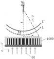
图20中则示出了焦距随波前移动的示意图,图20中,t为液晶盒的厚度(液晶盒厚),Δn为液晶和介质柱整体的折射率的变化量,波前对应L所在位置时焦距为f,而调整折射率之后,波前对应L’所在位置,此时的焦距为(f+Δf),也就是说,波前位置移动,则焦距就会相应移动。Figure 20 shows a schematic diagram of the focal length moving with the wavefront. In Figure 20, t is the thickness of the liquid crystal cell (the thickness of the liquid crystal cell), Δn is the change in the refractive index of the liquid crystal and the dielectric column as a whole, and the wavefront corresponds to where L is located. The focal length is f in position, and after adjusting the refractive index, the wavefront corresponds to the position of L', and the focal length at this time is (f+Δf), that is to say, the focal length will move accordingly if the position of the wavefront moves.
总的来说,本发明中,光束照射到纤维素粒子之后,光泳力占主导地位(且可能比散射力或梯度力大几个数量级),辐射效应引起纤维素粒子受热不均和热蠕变导致光泳力的产生,源自流体和气体介质中纤维素粒子的不均匀受热的光泳力通常是排斥性的,并且,光泳力试图将纤维素粒子推离最大光强度的区域,光束聚焦可以将纤维素粒子捕获,此时,激光照射到纤维素粒子上,通过超透镜可以调控纤维素粒子在三维空间内移动,随着纤维素粒子的移动,激光控制系统发出的激光会随着纤维素粒子移动,不断将对应的像素信号照射到纤维素粒子上,基于人眼的视觉残留,即可形成空间全色彩体成像。当然需要说明的是,也应设置超透镜中相应的液晶电压控制程序以便和激光控制系统进行匹配,从而实现任何图案在三维空间的显示,并且实现真三维显示设备的小型化。In general, in the present invention, after the light beam irradiates the cellulose particles, the photophoretic force dominates (and may be several orders of magnitude larger than the scattering force or gradient force), and the radiation effect causes the cellulose particles to be heated unevenly and thermally creep. This leads to the generation of photophoretic forces. Photophoretic forces originating from uneven heating of cellulose particles in fluid and gaseous media are usually repulsive and, as photophoretic forces try to push cellulose particles away from the region of maximum light intensity, beam focusing can The cellulose particles are captured. At this time, the laser is irradiated on the cellulose particles, and the movement of the cellulose particles in three-dimensional space can be regulated by the superlens. As the cellulose particles move, the laser emitted by the laser control system will follow the cellulose particles. Moving, and continuously irradiating the corresponding pixel signal to the cellulose particles, based on the visual residue of the human eye, a spatial full-color volume imaging can be formed. Of course, it should be noted that the corresponding liquid crystal voltage control program in the metalens should also be set to match the laser control system, so as to realize the display of any pattern in the three-dimensional space and realize the miniaturization of the true three-dimensional display device.
文中术语“第一”、“第二”仅用于描述目的,而不能理解为指示或暗示相对重要性或者隐含指明所指示的技术特征的数量。由此,限定有“第一”、“第二”的特征可以明示或者隐含地包括一个或者更多个该特征。在本发明的描述中,“多个”的含义是两个或两个以上,除非另有明确具体的限定。The terms "first" and "second" herein are only used for descriptive purposes, and should not be construed as indicating or implying relative importance or implying the number of indicated technical features. Thus, a feature defined as "first" or "second" may expressly or implicitly include one or more of that feature. In the description of the present invention, "plurality" means two or more, unless otherwise expressly and specifically defined.
在本说明书的描述中,参考术语“一个实施例”、“另一个实施例”、“一些实施例”、“一些具体实施例”或“另一些具体实施例”等的描述意指结合该实施例或示例描述的具体特征、结构、材料或者特点包含于本发明的至少一个实施例或示例中。在本说明书中,对上述术语的示意性表述不必须针对的是相同的实施例或示例。而且,描述的具体特征、结构、材料或者特点可以在任一个或多个实施例或示例中以合适的方式结合。此外,在不相互矛盾的情况下,本领域的技术人员可以将本说明书中描述的不同实施例或示例以及不同实施例或示例的特征进行结合和组合。In the description of this specification, references to the terms "one embodiment," "another embodiment," "some embodiments," "some specific embodiments," or "other specific embodiments" and the like are meant to be combined with the description A particular feature, structure, material, or characteristic described by an example or example is included in at least one embodiment or example of the present invention. In this specification, schematic representations of the above terms are not necessarily directed to the same embodiment or example. Furthermore, the particular features, structures, materials or characteristics described may be combined in any suitable manner in any one or more embodiments or examples. Furthermore, those skilled in the art may combine and combine the different embodiments or examples described in this specification, as well as the features of the different embodiments or examples, without conflicting each other.
尽管上面已经示出和描述了本发明的实施例,可以理解的是,上述实施例是示例性的,不能理解为对本发明的限制,本领域的普通技术人员在本发明的范围内可以对上述实施例进行变化、修改、替换和变型。Although the embodiments of the present invention have been shown and described above, it should be understood that the above-mentioned embodiments are exemplary and should not be construed as limiting the present invention. Embodiments are subject to variations, modifications, substitutions and variations.
Claims (13)
Translated fromChinesePriority Applications (2)
| Application Number | Priority Date | Filing Date | Title |
|---|---|---|---|
| CN202210442747.7ACN114859607A (en) | 2022-04-25 | 2022-04-25 | Superlens, manufacturing method thereof and display device |
| PCT/CN2023/090414WO2023207926A1 (en) | 2022-04-25 | 2023-04-24 | Superlens and manufacturing method therefor, and display apparatus |
Applications Claiming Priority (1)
| Application Number | Priority Date | Filing Date | Title |
|---|---|---|---|
| CN202210442747.7ACN114859607A (en) | 2022-04-25 | 2022-04-25 | Superlens, manufacturing method thereof and display device |
Publications (1)
| Publication Number | Publication Date |
|---|---|
| CN114859607Atrue CN114859607A (en) | 2022-08-05 |
Family
ID=82633489
Family Applications (1)
| Application Number | Title | Priority Date | Filing Date |
|---|---|---|---|
| CN202210442747.7APendingCN114859607A (en) | 2022-04-25 | 2022-04-25 | Superlens, manufacturing method thereof and display device |
Country Status (2)
| Country | Link |
|---|---|
| CN (1) | CN114859607A (en) |
| WO (1) | WO2023207926A1 (en) |
Cited By (2)
| Publication number | Priority date | Publication date | Assignee | Title |
|---|---|---|---|---|
| CN115332938A (en)* | 2022-08-22 | 2022-11-11 | 北京京东方技术开发有限公司 | Laser transmitter and laser detection device |
| WO2023207926A1 (en)* | 2022-04-25 | 2023-11-02 | 京东方科技集团股份有限公司 | Superlens and manufacturing method therefor, and display apparatus |
Citations (19)
| Publication number | Priority date | Publication date | Assignee | Title |
|---|---|---|---|---|
| CN102243402A (en)* | 2011-07-13 | 2011-11-16 | 深圳超多维光电子有限公司 | Liquid crystal lens grating and stereo display device thereof |
| CN203433171U (en)* | 2013-08-21 | 2014-02-12 | 信利光电股份有限公司 | Zoom lens and camera module |
| CN103913879A (en)* | 2014-04-14 | 2014-07-09 | 重庆卓美华视光电有限公司 | Liquid crystal lens, method for forming same and stereoscopic display device |
| CN104020625A (en)* | 2014-06-25 | 2014-09-03 | 重庆卓美华视光电有限公司 | 3D (Three Dimensional) optical splitter and three-dimensional display device |
| CN206002779U (en)* | 2016-09-14 | 2017-03-08 | 合肥鑫晟光电科技有限公司 | Naked eye three-dimensional display device |
| CN106970483A (en)* | 2016-01-13 | 2017-07-21 | 三星电子株式会社 | Tunable electro-optic wave filter |
| US20170277012A1 (en)* | 2016-03-25 | 2017-09-28 | Samsung Display Co., Ltd. | Liquid crystal lens and display device including the same |
| CN107422570A (en)* | 2017-08-16 | 2017-12-01 | 集美大学 | double-layer liquid crystal lens device and preparation method thereof |
| CN108873505A (en)* | 2018-07-27 | 2018-11-23 | 京东方科技集团股份有限公司 | Liquid crystal lens, mould group, augmented reality equipment, glasses, display methods |
| CN110192145A (en)* | 2016-11-18 | 2019-08-30 | 奇跃公司 | Liquid crystal diffraction device having nano-scale pattern and method of fabricating the same |
| CN111103739A (en)* | 2019-12-31 | 2020-05-05 | 中国工程物理研究院流体物理研究所 | Electric control zoom plane lens |
| CN111290164A (en)* | 2020-03-31 | 2020-06-16 | 京东方科技集团股份有限公司 | Transparent display panel, display device and glasses |
| CN111722423A (en)* | 2020-06-22 | 2020-09-29 | 中国科学院上海光学精密机械研究所 | Continuously Variable Focus Metalens Combining Liquid Crystals and Metasurfaces |
| CN111880347A (en)* | 2020-08-27 | 2020-11-03 | 南京南辉智能光学感控研究院有限公司 | Terahertz lens with adjustable focal length and preparation method and application thereof |
| CN112099285A (en)* | 2020-11-03 | 2020-12-18 | 南昌虚拟现实研究院股份有限公司 | Liquid crystal lens device and virtual reality zooming method |
| CN113467117A (en)* | 2021-07-06 | 2021-10-01 | 南京大学 | Temperature-controlled vector vortex light beam detector, preparation method thereof and detection device |
| CN113504678A (en)* | 2021-07-22 | 2021-10-15 | 北京京东方技术开发有限公司 | Lens, depth of field sensor, depth of field measuring system and manufacturing method of lens |
| CN113589535A (en)* | 2021-08-16 | 2021-11-02 | 北京京东方技术开发有限公司 | Optical imaging system and head-mounted display device |
| CN113687515A (en)* | 2021-09-01 | 2021-11-23 | 北京京东方技术开发有限公司 | Near-to-eye display device, preparation method and wearable equipment |
Family Cites Families (5)
| Publication number | Priority date | Publication date | Assignee | Title |
|---|---|---|---|---|
| CN203858434U (en)* | 2014-04-14 | 2014-10-01 | 重庆卓美华视光电有限公司 | Liquid crystal lens and three-dimensional display device |
| CN208384249U (en)* | 2018-07-27 | 2019-01-15 | 京东方科技集团股份有限公司 | A kind of AR glasses |
| CN111399262B (en)* | 2020-04-27 | 2023-10-31 | 南京南辉智能光学感控研究院有限公司 | Adjustable terahertz lens and preparation method and application thereof |
| CN212647221U (en)* | 2020-08-27 | 2021-03-02 | 南京南辉智能光学感控研究院有限公司 | Terahertz lens with adjustable focal length |
| CN114859607A (en)* | 2022-04-25 | 2022-08-05 | 北京京东方技术开发有限公司 | Superlens, manufacturing method thereof and display device |
- 2022
- 2022-04-25CNCN202210442747.7Apatent/CN114859607A/enactivePending
- 2023
- 2023-04-24WOPCT/CN2023/090414patent/WO2023207926A1/ennot_activeCeased
Patent Citations (19)
| Publication number | Priority date | Publication date | Assignee | Title |
|---|---|---|---|---|
| CN102243402A (en)* | 2011-07-13 | 2011-11-16 | 深圳超多维光电子有限公司 | Liquid crystal lens grating and stereo display device thereof |
| CN203433171U (en)* | 2013-08-21 | 2014-02-12 | 信利光电股份有限公司 | Zoom lens and camera module |
| CN103913879A (en)* | 2014-04-14 | 2014-07-09 | 重庆卓美华视光电有限公司 | Liquid crystal lens, method for forming same and stereoscopic display device |
| CN104020625A (en)* | 2014-06-25 | 2014-09-03 | 重庆卓美华视光电有限公司 | 3D (Three Dimensional) optical splitter and three-dimensional display device |
| CN106970483A (en)* | 2016-01-13 | 2017-07-21 | 三星电子株式会社 | Tunable electro-optic wave filter |
| US20170277012A1 (en)* | 2016-03-25 | 2017-09-28 | Samsung Display Co., Ltd. | Liquid crystal lens and display device including the same |
| CN206002779U (en)* | 2016-09-14 | 2017-03-08 | 合肥鑫晟光电科技有限公司 | Naked eye three-dimensional display device |
| CN110192145A (en)* | 2016-11-18 | 2019-08-30 | 奇跃公司 | Liquid crystal diffraction device having nano-scale pattern and method of fabricating the same |
| CN107422570A (en)* | 2017-08-16 | 2017-12-01 | 集美大学 | double-layer liquid crystal lens device and preparation method thereof |
| CN108873505A (en)* | 2018-07-27 | 2018-11-23 | 京东方科技集团股份有限公司 | Liquid crystal lens, mould group, augmented reality equipment, glasses, display methods |
| CN111103739A (en)* | 2019-12-31 | 2020-05-05 | 中国工程物理研究院流体物理研究所 | Electric control zoom plane lens |
| CN111290164A (en)* | 2020-03-31 | 2020-06-16 | 京东方科技集团股份有限公司 | Transparent display panel, display device and glasses |
| CN111722423A (en)* | 2020-06-22 | 2020-09-29 | 中国科学院上海光学精密机械研究所 | Continuously Variable Focus Metalens Combining Liquid Crystals and Metasurfaces |
| CN111880347A (en)* | 2020-08-27 | 2020-11-03 | 南京南辉智能光学感控研究院有限公司 | Terahertz lens with adjustable focal length and preparation method and application thereof |
| CN112099285A (en)* | 2020-11-03 | 2020-12-18 | 南昌虚拟现实研究院股份有限公司 | Liquid crystal lens device and virtual reality zooming method |
| CN113467117A (en)* | 2021-07-06 | 2021-10-01 | 南京大学 | Temperature-controlled vector vortex light beam detector, preparation method thereof and detection device |
| CN113504678A (en)* | 2021-07-22 | 2021-10-15 | 北京京东方技术开发有限公司 | Lens, depth of field sensor, depth of field measuring system and manufacturing method of lens |
| CN113589535A (en)* | 2021-08-16 | 2021-11-02 | 北京京东方技术开发有限公司 | Optical imaging system and head-mounted display device |
| CN113687515A (en)* | 2021-09-01 | 2021-11-23 | 北京京东方技术开发有限公司 | Near-to-eye display device, preparation method and wearable equipment |
Non-Patent Citations (1)
| Title |
|---|
| D. E. SMALLEY,ETALS: "A photophoretic-trap volumetric display", vol. 553, pages 486 - 490* |
Cited By (2)
| Publication number | Priority date | Publication date | Assignee | Title |
|---|---|---|---|---|
| WO2023207926A1 (en)* | 2022-04-25 | 2023-11-02 | 京东方科技集团股份有限公司 | Superlens and manufacturing method therefor, and display apparatus |
| CN115332938A (en)* | 2022-08-22 | 2022-11-11 | 北京京东方技术开发有限公司 | Laser transmitter and laser detection device |
Also Published As
| Publication number | Publication date |
|---|---|
| WO2023207926A1 (en) | 2023-11-02 |
Similar Documents
| Publication | Publication Date | Title |
|---|---|---|
| US11086065B2 (en) | Diffractive grating with variable diffraction efficiency and method for displaying an image | |
| WO2023207926A1 (en) | Superlens and manufacturing method therefor, and display apparatus | |
| CN103631056B (en) | Variable optical retarder | |
| JP2023041678A (en) | Improved manufacturing for virtual and augmented reality system and component | |
| US11822190B2 (en) | Spatial light modulator and method of forming the same | |
| Lei et al. | An electrically tunable plenoptic camera using a liquid crystal microlens array | |
| US20190086699A1 (en) | Display device and display method thereof | |
| CN103217849B (en) | A kind of focus adjustable liquid crystal microlens array | |
| CN103076706B (en) | Focal length adjustable liquid crystal micro-lens array | |
| JP2004101885A (en) | Liquid crystal lens and its driving method, and device | |
| Peng et al. | Metalens in improving imaging quality: advancements, challenges, and prospects for future display | |
| CN109031811A (en) | A kind of focal length and the variable liquid crystal optical device of phase-delay quantity | |
| CN113687515A (en) | Near-to-eye display device, preparation method and wearable equipment | |
| TWI483004B (en) | Electro-modulating liquid crystal lens group with central electrode | |
| CN104076518A (en) | Novel pixel structure for three-dimensional light field dynamic displaying | |
| Yu et al. | Large aperture liquid crystal lens array based on integrated composite electrodes for 2D/3D switchable displays | |
| Zhang et al. | Stacked high-resistance layer induced dual-focal liquid crystal microlens array for enhanced depth-of-field integral imaging 3D display | |
| JP5205077B2 (en) | Liquid crystal optical element | |
| CN110737145A (en) | Variable focus lens and display device | |
| KR20140112271A (en) | Spatial light modulator, apparatus for holography 3-dimensional display and method for modulating spatial light | |
| CN108051936B (en) | Display panel and driving method thereof, display device and driving method thereof | |
| CN115685638A (en) | Composite liquid crystal lens, preparation method, display device and display method | |
| US20240027823A1 (en) | Multi-focusing meta lens | |
| US10156769B2 (en) | Two-dimensional beam steering device | |
| CN117872640A (en) | A reflective spatial light modulator based on a metasurface and a manufacturing method thereof |
Legal Events
| Date | Code | Title | Description |
|---|---|---|---|
| PB01 | Publication | ||
| PB01 | Publication | ||
| SE01 | Entry into force of request for substantive examination | ||
| SE01 | Entry into force of request for substantive examination |