CN114859367A - Optical interferometric proximity sensor with optical path extender - Google Patents
Optical interferometric proximity sensor with optical path extenderDownload PDFInfo
- Publication number
- CN114859367A CN114859367ACN202210100812.8ACN202210100812ACN114859367ACN 114859367 ACN114859367 ACN 114859367ACN 202210100812 ACN202210100812 ACN 202210100812ACN 114859367 ACN114859367 ACN 114859367A
- Authority
- CN
- China
- Prior art keywords
- proximity sensor
- optical path
- optical
- electronic device
- optical proximity
- Prior art date
- Legal status (The legal status is an assumption and is not a legal conclusion. Google has not performed a legal analysis and makes no representation as to the accuracy of the status listed.)
- Pending
Links
Images


Classifications
- G—PHYSICS
- G01—MEASURING; TESTING
- G01S—RADIO DIRECTION-FINDING; RADIO NAVIGATION; DETERMINING DISTANCE OR VELOCITY BY USE OF RADIO WAVES; LOCATING OR PRESENCE-DETECTING BY USE OF THE REFLECTION OR RERADIATION OF RADIO WAVES; ANALOGOUS ARRANGEMENTS USING OTHER WAVES
- G01S7/00—Details of systems according to groups G01S13/00, G01S15/00, G01S17/00
- G01S7/48—Details of systems according to groups G01S13/00, G01S15/00, G01S17/00 of systems according to group G01S17/00
- G01S7/491—Details of non-pulse systems
- G01S7/4911—Transmitters
- G—PHYSICS
- G01—MEASURING; TESTING
- G01S—RADIO DIRECTION-FINDING; RADIO NAVIGATION; DETERMINING DISTANCE OR VELOCITY BY USE OF RADIO WAVES; LOCATING OR PRESENCE-DETECTING BY USE OF THE REFLECTION OR RERADIATION OF RADIO WAVES; ANALOGOUS ARRANGEMENTS USING OTHER WAVES
- G01S7/00—Details of systems according to groups G01S13/00, G01S15/00, G01S17/00
- G01S7/48—Details of systems according to groups G01S13/00, G01S15/00, G01S17/00 of systems according to group G01S17/00
- G01S7/491—Details of non-pulse systems
- G01S7/4912—Receivers
- G01S7/4916—Receivers using self-mixing in the laser cavity
- G—PHYSICS
- G01—MEASURING; TESTING
- G01S—RADIO DIRECTION-FINDING; RADIO NAVIGATION; DETERMINING DISTANCE OR VELOCITY BY USE OF RADIO WAVES; LOCATING OR PRESENCE-DETECTING BY USE OF THE REFLECTION OR RERADIATION OF RADIO WAVES; ANALOGOUS ARRANGEMENTS USING OTHER WAVES
- G01S17/00—Systems using the reflection or reradiation of electromagnetic waves other than radio waves, e.g. lidar systems
- G01S17/02—Systems using the reflection of electromagnetic waves other than radio waves
- G01S17/50—Systems of measurement based on relative movement of target
- G01S17/58—Velocity or trajectory determination systems; Sense-of-movement determination systems
- G—PHYSICS
- G01—MEASURING; TESTING
- G01B—MEASURING LENGTH, THICKNESS OR SIMILAR LINEAR DIMENSIONS; MEASURING ANGLES; MEASURING AREAS; MEASURING IRREGULARITIES OF SURFACES OR CONTOURS
- G01B11/00—Measuring arrangements characterised by the use of optical techniques
- G01B11/14—Measuring arrangements characterised by the use of optical techniques for measuring distance or clearance between spaced objects or spaced apertures
- G—PHYSICS
- G01—MEASURING; TESTING
- G01B—MEASURING LENGTH, THICKNESS OR SIMILAR LINEAR DIMENSIONS; MEASURING ANGLES; MEASURING AREAS; MEASURING IRREGULARITIES OF SURFACES OR CONTOURS
- G01B9/00—Measuring instruments characterised by the use of optical techniques
- G01B9/02—Interferometers
- G01B9/02015—Interferometers characterised by the beam path configuration
- G—PHYSICS
- G01—MEASURING; TESTING
- G01B—MEASURING LENGTH, THICKNESS OR SIMILAR LINEAR DIMENSIONS; MEASURING ANGLES; MEASURING AREAS; MEASURING IRREGULARITIES OF SURFACES OR CONTOURS
- G01B9/00—Measuring instruments characterised by the use of optical techniques
- G01B9/02—Interferometers
- G01B9/02049—Interferometers characterised by particular mechanical design details
- G01B9/02054—Hand held
- G—PHYSICS
- G01—MEASURING; TESTING
- G01B—MEASURING LENGTH, THICKNESS OR SIMILAR LINEAR DIMENSIONS; MEASURING ANGLES; MEASURING AREAS; MEASURING IRREGULARITIES OF SURFACES OR CONTOURS
- G01B9/00—Measuring instruments characterised by the use of optical techniques
- G01B9/02—Interferometers
- G01B9/02092—Self-mixing interferometers, i.e. feedback of light from object into laser cavity
- G—PHYSICS
- G01—MEASURING; TESTING
- G01S—RADIO DIRECTION-FINDING; RADIO NAVIGATION; DETERMINING DISTANCE OR VELOCITY BY USE OF RADIO WAVES; LOCATING OR PRESENCE-DETECTING BY USE OF THE REFLECTION OR RERADIATION OF RADIO WAVES; ANALOGOUS ARRANGEMENTS USING OTHER WAVES
- G01S17/00—Systems using the reflection or reradiation of electromagnetic waves other than radio waves, e.g. lidar systems
- G01S17/02—Systems using the reflection of electromagnetic waves other than radio waves
- G01S17/06—Systems determining position data of a target
- G01S17/08—Systems determining position data of a target for measuring distance only
- G—PHYSICS
- G01—MEASURING; TESTING
- G01S—RADIO DIRECTION-FINDING; RADIO NAVIGATION; DETERMINING DISTANCE OR VELOCITY BY USE OF RADIO WAVES; LOCATING OR PRESENCE-DETECTING BY USE OF THE REFLECTION OR RERADIATION OF RADIO WAVES; ANALOGOUS ARRANGEMENTS USING OTHER WAVES
- G01S17/00—Systems using the reflection or reradiation of electromagnetic waves other than radio waves, e.g. lidar systems
- G01S17/02—Systems using the reflection of electromagnetic waves other than radio waves
- G01S17/06—Systems determining position data of a target
- G01S17/46—Indirect determination of position data
- G01S17/48—Active triangulation systems, i.e. using the transmission and reflection of electromagnetic waves other than radio waves
- G—PHYSICS
- G01—MEASURING; TESTING
- G01S—RADIO DIRECTION-FINDING; RADIO NAVIGATION; DETERMINING DISTANCE OR VELOCITY BY USE OF RADIO WAVES; LOCATING OR PRESENCE-DETECTING BY USE OF THE REFLECTION OR RERADIATION OF RADIO WAVES; ANALOGOUS ARRANGEMENTS USING OTHER WAVES
- G01S7/00—Details of systems according to groups G01S13/00, G01S15/00, G01S17/00
- G01S7/48—Details of systems according to groups G01S13/00, G01S15/00, G01S17/00 of systems according to group G01S17/00
- G01S7/481—Constructional features, e.g. arrangements of optical elements
- G01S7/4811—Constructional features, e.g. arrangements of optical elements common to transmitter and receiver
- G01S7/4812—Constructional features, e.g. arrangements of optical elements common to transmitter and receiver transmitted and received beams following a coaxial path
- G—PHYSICS
- G01—MEASURING; TESTING
- G01S—RADIO DIRECTION-FINDING; RADIO NAVIGATION; DETERMINING DISTANCE OR VELOCITY BY USE OF RADIO WAVES; LOCATING OR PRESENCE-DETECTING BY USE OF THE REFLECTION OR RERADIATION OF RADIO WAVES; ANALOGOUS ARRANGEMENTS USING OTHER WAVES
- G01S7/00—Details of systems according to groups G01S13/00, G01S15/00, G01S17/00
- G01S7/48—Details of systems according to groups G01S13/00, G01S15/00, G01S17/00 of systems according to group G01S17/00
- G01S7/481—Constructional features, e.g. arrangements of optical elements
- G01S7/4814—Constructional features, e.g. arrangements of optical elements of transmitters alone
- G—PHYSICS
- G01—MEASURING; TESTING
- G01S—RADIO DIRECTION-FINDING; RADIO NAVIGATION; DETERMINING DISTANCE OR VELOCITY BY USE OF RADIO WAVES; LOCATING OR PRESENCE-DETECTING BY USE OF THE REFLECTION OR RERADIATION OF RADIO WAVES; ANALOGOUS ARRANGEMENTS USING OTHER WAVES
- G01S7/00—Details of systems according to groups G01S13/00, G01S15/00, G01S17/00
- G01S7/48—Details of systems according to groups G01S13/00, G01S15/00, G01S17/00 of systems according to group G01S17/00
- G01S7/491—Details of non-pulse systems
- G01S7/4912—Receivers
- G01S7/4913—Circuits for detection, sampling, integration or read-out
- G—PHYSICS
- G01—MEASURING; TESTING
- G01S—RADIO DIRECTION-FINDING; RADIO NAVIGATION; DETERMINING DISTANCE OR VELOCITY BY USE OF RADIO WAVES; LOCATING OR PRESENCE-DETECTING BY USE OF THE REFLECTION OR RERADIATION OF RADIO WAVES; ANALOGOUS ARRANGEMENTS USING OTHER WAVES
- G01S7/00—Details of systems according to groups G01S13/00, G01S15/00, G01S17/00
- G01S7/48—Details of systems according to groups G01S13/00, G01S15/00, G01S17/00 of systems according to group G01S17/00
- G01S7/497—Means for monitoring or calibrating
- G—PHYSICS
- G01—MEASURING; TESTING
- G01V—GEOPHYSICS; GRAVITATIONAL MEASUREMENTS; DETECTING MASSES OR OBJECTS; TAGS
- G01V8/00—Prospecting or detecting by optical means
- G01V8/10—Detecting, e.g. by using light barriers
- G01V8/12—Detecting, e.g. by using light barriers using one transmitter and one receiver
- G01V8/14—Detecting, e.g. by using light barriers using one transmitter and one receiver using reflectors
- G—PHYSICS
- G06—COMPUTING OR CALCULATING; COUNTING
- G06F—ELECTRIC DIGITAL DATA PROCESSING
- G06F3/00—Input arrangements for transferring data to be processed into a form capable of being handled by the computer; Output arrangements for transferring data from processing unit to output unit, e.g. interface arrangements
- G06F3/01—Input arrangements or combined input and output arrangements for interaction between user and computer
- G06F3/017—Gesture based interaction, e.g. based on a set of recognized hand gestures
- H—ELECTRICITY
- H01—ELECTRIC ELEMENTS
- H01S—DEVICES USING THE PROCESS OF LIGHT AMPLIFICATION BY STIMULATED EMISSION OF RADIATION [LASER] TO AMPLIFY OR GENERATE LIGHT; DEVICES USING STIMULATED EMISSION OF ELECTROMAGNETIC RADIATION IN WAVE RANGES OTHER THAN OPTICAL
- H01S5/00—Semiconductor lasers
- H01S5/10—Construction or shape of the optical resonator, e.g. extended or external cavity, coupled cavities, bent-guide, varying width, thickness or composition of the active region
- H01S5/18—Surface-emitting [SE] lasers, e.g. having both horizontal and vertical cavities
- H01S5/183—Surface-emitting [SE] lasers, e.g. having both horizontal and vertical cavities having only vertical cavities, e.g. vertical cavity surface-emitting lasers [VCSEL]
- G—PHYSICS
- G01—MEASURING; TESTING
- G01S—RADIO DIRECTION-FINDING; RADIO NAVIGATION; DETERMINING DISTANCE OR VELOCITY BY USE OF RADIO WAVES; LOCATING OR PRESENCE-DETECTING BY USE OF THE REFLECTION OR RERADIATION OF RADIO WAVES; ANALOGOUS ARRANGEMENTS USING OTHER WAVES
- G01S17/00—Systems using the reflection or reradiation of electromagnetic waves other than radio waves, e.g. lidar systems
- G01S17/02—Systems using the reflection of electromagnetic waves other than radio waves
- G01S17/06—Systems determining position data of a target
- G01S17/08—Systems determining position data of a target for measuring distance only
- G01S17/32—Systems determining position data of a target for measuring distance only using transmission of continuous waves, whether amplitude-, frequency-, or phase-modulated, or unmodulated
- G01S17/34—Systems determining position data of a target for measuring distance only using transmission of continuous waves, whether amplitude-, frequency-, or phase-modulated, or unmodulated using transmission of continuous, frequency-modulated waves while heterodyning the received signal, or a signal derived therefrom, with a locally-generated signal related to the contemporaneously transmitted signal
- G—PHYSICS
- G01—MEASURING; TESTING
- G01S—RADIO DIRECTION-FINDING; RADIO NAVIGATION; DETERMINING DISTANCE OR VELOCITY BY USE OF RADIO WAVES; LOCATING OR PRESENCE-DETECTING BY USE OF THE REFLECTION OR RERADIATION OF RADIO WAVES; ANALOGOUS ARRANGEMENTS USING OTHER WAVES
- G01S17/00—Systems using the reflection or reradiation of electromagnetic waves other than radio waves, e.g. lidar systems
- G01S17/02—Systems using the reflection of electromagnetic waves other than radio waves
- G01S17/06—Systems determining position data of a target
- G01S17/08—Systems determining position data of a target for measuring distance only
- G01S17/32—Systems determining position data of a target for measuring distance only using transmission of continuous waves, whether amplitude-, frequency-, or phase-modulated, or unmodulated
- G01S17/36—Systems determining position data of a target for measuring distance only using transmission of continuous waves, whether amplitude-, frequency-, or phase-modulated, or unmodulated with phase comparison between the received signal and the contemporaneously transmitted signal
Landscapes
- Physics & Mathematics (AREA)
- Engineering & Computer Science (AREA)
- General Physics & Mathematics (AREA)
- Radar, Positioning & Navigation (AREA)
- Remote Sensing (AREA)
- Computer Networks & Wireless Communication (AREA)
- Electromagnetism (AREA)
- Optics & Photonics (AREA)
- General Engineering & Computer Science (AREA)
- Theoretical Computer Science (AREA)
- Condensed Matter Physics & Semiconductors (AREA)
- Geophysics (AREA)
- General Life Sciences & Earth Sciences (AREA)
- Life Sciences & Earth Sciences (AREA)
- Human Computer Interaction (AREA)
- Length Measuring Devices By Optical Means (AREA)
- Measurement Of Optical Distance (AREA)
- Optical Radar Systems And Details Thereof (AREA)
Abstract
Translated fromChinese
Description
Translated fromChinese技术领域technical field
本文描述的实施方案涉及光学传感器,并且具体地涉及被配置为确定到对象的距离和/或对象的速度的光学干涉测量接近传感器。Embodiments described herein relate to optical sensors, and in particular to optical interferometric proximity sensors configured to determine the distance to an object and/or the velocity of the object.
背景技术Background technique
电子设备可以包括系统或传感器—在本文中称为“接近传感器”—用于测量或估计自由空间的该电子设备与对象或表面(诸如电子设备的用户)分离的距离。然而,常规接近传感器可能需要沿着光学路径的自由空间来实现令人满意的感测性能,这会导致接近传感器和它们所部署在的设备的厚度增加。An electronic device may include a system or sensor—referred to herein as a “proximity sensor”—for measuring or estimating the distance in free space that the electronic device is separated from an object or surface, such as a user of the electronic device. However, conventional proximity sensors may require free space along the optical path to achieve satisfactory sensing performance, which results in increased thickness of the proximity sensors and the devices in which they are deployed.
发明内容SUMMARY OF THE INVENTION
本文描述的实施方案涉及包括光学路径延伸器的光学接近传感器。光学路径延伸器可以定位在光源与光学接近传感器的外壳中的孔之间。光源被配置为照射对象并收集回射信号以基于自混合干涉法确定到该对象的距离和/或该对象的速度。光学路径延伸器可以增加光学接近传感器的光学路径长度,从而允许光学接近传感器与传统光学接近传感器相比具有减小的厚度,同时实现类似或改进的感测性能。Embodiments described herein relate to optical proximity sensors that include optical path extenders. The optical path extender can be positioned between the light source and the hole in the housing of the optical proximity sensor. The light source is configured to illuminate the object and collect retroreflected signals to determine the distance to the object and/or the speed of the object based on self-mixing interferometry. The optical path extender can increase the optical path length of the optical proximity sensor, thereby allowing the optical proximity sensor to have a reduced thickness compared to conventional optical proximity sensors, while achieving similar or improved sensing performance.
附图说明Description of drawings
现在将参考在附图示出的代表性实施方案。应当理解,以下描述并非旨在将本公开限制于一个所包括的实施方案。相反,本文提供的该公开旨在涵盖可被包括在所述实施方案的实质和范围内并由所附权利要求限定的替代形式、修改形式和等同形式。Reference will now be made to representative embodiments illustrated in the accompanying drawings. It should be understood that the following description is not intended to limit the disclosure to one included embodiment. On the contrary, the disclosure provided herein is intended to cover alternatives, modifications and equivalents, which may be included within the spirit and scope of the described embodiments and as defined by the appended claims.
图1描绘了诸如本文所述结合接近传感器以确定到电子设备附近的对象的距离和/或该对象的速度的电子设备的示意图。1 depicts a schematic diagram of an electronic device, such as described herein, incorporating a proximity sensor to determine the distance to and/or velocity of an object in the vicinity of the electronic device.
图2示出了具有与VCSEL光源集成的光学路径延伸器的示例性光学接近传感器。Figure 2 shows an exemplary optical proximity sensor with an optical path extender integrated with a VCSEL light source.
图3A至图3B示出了示例性光学接近传感器,其包括重定向特征以增加光学接近传感器的光学路径长度。3A-3B illustrate an example optical proximity sensor that includes redirection features to increase the optical path length of the optical proximity sensor.
图4A至图4B示出了示例性光学接近传感器,其包括光子部件以增加光学接近传感器的光学路径长度。4A-4B illustrate an example optical proximity sensor that includes photonic components to increase the optical path length of the optical proximity sensor.
图5A描绘了诸如本文所述结合接近传感器以确定到电子设备附近的对象的距离和/或该对象的速度的另一电子设备的示意图。5A depicts a schematic diagram of another electronic device, such as described herein, incorporating a proximity sensor to determine the distance to and/or velocity of an object in the vicinity of the electronic device.
图5B描绘了诸如本文所述结合接近传感器以确定到电子设备的可移动表面的距离和/或该可移动表面的速度的另一电子设备的示意图。5B depicts a schematic diagram of another electronic device such as described herein incorporating a proximity sensor to determine the distance to and/or velocity of a movable surface of an electronic device.
图6A描绘了诸如本文所述结合接近传感器以确定用户的手指相对于电子设备的输入区域的距离和/或速度的电子设备的示意图。6A depicts a schematic diagram of an electronic device such as described herein incorporating a proximity sensor to determine the distance and/or velocity of a user's finger relative to an input area of the electronic device.
图6B描绘了诸如本文所述结合接近传感器以确定用户的手指相对于电子设备的触摸输入区域的距离和/或速度的电子设备的示意图。6B depicts a schematic diagram of an electronic device such as described herein incorporating a proximity sensor to determine the distance and/or velocity of a user's finger relative to a touch input area of the electronic device.
图6C描绘了诸如本文所述结合接近传感器以确定到电子设备的用户可以对其施加力的电子设备的可移动表面的距离和/或该电子设备的可移动表面的速度的电子设备的示意图。6C depicts a schematic diagram of an electronic device such as described herein incorporating a proximity sensor to determine the distance and/or velocity of a movable surface of the electronic device to which a user of the electronic device may apply force.
图6D描绘了诸如本文所述结合接近传感器以确定到电子设备的用户可以对其施加力的电子设备的可移动表面的距离和/或该电子设备的可移动表面的速度的电子设备的另一个示意图。6D depicts another electronic device such as described herein incorporating a proximity sensor to determine the distance to and/or the velocity of the movable surface of the electronic device to which a user of the electronic device may apply force Schematic.
图7为描绘了诸如本文所述的操作接近传感器的一种方法的示例性操作的流程图。7 is a flowchart depicting exemplary operations of a method of operating a proximity sensor, such as described herein.
图8示出了可以执行本文所述的操作的电子设备的样本电气框图。8 shows a sample electrical block diagram of an electronic device that can perform the operations described herein.
在不同附图中使用相同或相似的附图标记来指示相似、相关或者相同的项目。The use of the same or similar reference numbers in different figures indicates similar, related or identical items.
附图中的交叉影线或阴影的使用通常被提供以阐明相邻元件之间的边界并有利于附图的易读性。因此,存在或不存在无交叉影线或阴影均不表示或指示对特定材料、材料特性、元件比例、元件尺寸、类似图示元件的共同性或在附图中所示的任何元件的任何其他特征、属性、或特性的任何偏好或要求。The use of cross-hatching or hatching in the figures is generally provided to clarify boundaries between adjacent elements and to facilitate the legibility of the figures. Accordingly, the presence or absence of non-cross-hatching or hatching does not represent or indicate specific materials, material properties, proportions of elements, dimensions of elements, commonality with similar illustrated elements, or any other commonality with any of the elements shown in the figures. any preference or requirement for characteristics, attributes, or characteristics.
类似地,某些附图包括通过可由一个或多个光子采取的一种或多种介质的一个或多个示例性路径的矢量、射线、迹线和/或其他视觉表示,该一个或多个示例性路径可包括反射、折射、衍射等,该一个或多个光子源自附图所示或在一些情况下从附图中省略的一个或多个光源。应当理解,提供这些光的简化视觉表示仅仅是为了便于理解本文所述的各种实施方案,并且因此可以不必按比例或以角度精度或准确度呈现或示出,并且因此,并不旨在表明除了本文描述或引用的其他实施方案之外,所示实施方案以任何特定所示的角度、取向、偏振、颜色或方向接收、发射、反射、折射、聚焦和/或衍射光的任何偏好或要求。Similarly, certain figures include vectors, rays, traces and/or other visual representations of one or more exemplary paths through one or more media that may be taken by one or more photons, the one or more Exemplary paths may include reflection, refraction, diffraction, etc., the one or more photons originating from one or more light sources shown or in some cases omitted from the figures. It should be understood that these simplified visual representations of lights are provided merely to facilitate understanding of the various embodiments described herein, and thus may not necessarily be presented or illustrated to scale or with angular precision or accuracy, and are therefore not intended to suggest Any preference or requirement for the illustrated embodiments to receive, emit, reflect, refract, focus and/or diffract light at any particular illustrated angle, orientation, polarization, color or direction, in addition to other embodiments described or referenced herein .
附加地,应当理解,各个特征部和元件(以及其集合和分组)的比例和尺寸(相对的或绝对的)以及其间呈现的界限、间距和位置关系在附图中被提供,以仅用于促进对本文所述的各个实施方案的理解,并因此可不必要地被呈现或示出以进行缩放并且并非旨在指示对所示的实施方案的任何偏好或要求,以排除结合其所述的实施方案。Additionally, it is to be understood that the proportions and dimensions (relative or absolute) of the various features and elements (as well as sets and groupings thereof), as well as the boundaries, spacings and positional relationships presented therebetween, are provided in the drawings for purposes only of to facilitate understanding of the various embodiments described herein, and thus may be presented or shown unnecessarily to scale and is not intended to indicate any preference or requirement for the embodiments shown in order to preclude implementations described in connection therewith Program.
具体实施方式Detailed ways
本文描述的实施方案涉及用于电子设备的光学接近传感器。这些实施方案通常包括垂直腔面发射激光器(“VCSEL”),该VCSEL被定向成朝着光学接近传感器附近的对象辐射光束,以便确定到该对象的距离和/或该对象相对于所述光学接近传感器的速度。可以基于辐射光束从对象的外表面的反射来确定到对象的距离和/或对象的速度。对象可以在结合光学接近传感器的电子设备内部或外部。光束可以具有根据特定模式调制的波长,在本文中称为“波长调制”。Embodiments described herein relate to optical proximity sensors for electronic devices. These embodiments typically include a vertical cavity surface emitting laser ("VCSEL") directed to radiate a beam toward an object in the vicinity of an optical proximity sensor in order to determine the distance to the object and/or the object's relative proximity to the optical proximity sensor the speed of the sensor. The distance to the object and/or the speed of the object may be determined based on the reflection of the radiation beam from the outer surface of the object. Objects can be inside or outside of electronic devices incorporating optical proximity sensors. The light beam may have a wavelength modulated according to a particular pattern, referred to herein as "wavelength modulation".
光学接近传感器可以包括一个或多个光学路径延伸器,以通过延伸光学接近传感器的光学路径长度来减小光学接近传感器的厚度。因此,光学接近传感器可以占据电子设备中较少的空间,和/或光学接近传感器可以放置在与传统的光学接近传感器相比更小的、更薄的设备中。The optical proximity sensor may include one or more optical path extenders to reduce the thickness of the optical proximity sensor by extending the optical path length of the optical proximity sensor. Accordingly, optical proximity sensors can occupy less space in electronic devices, and/or optical proximity sensors can be placed in smaller, thinner devices than conventional optical proximity sensors.
光学路径延伸器可以以多种方式中的任何方式延伸光学接近传感器的光学路径长度。在一些情况下,光学路径延伸器可以是沿穿过光学接近传感器的光学路径定位的高折射率材料。在一些情况下,光学路径延伸器可以与VCSEL光源集成,例如作为VCSEL光源的衬底,如关于图2更详细地讨论的。The optical path extender may extend the optical path length of the optical proximity sensor in any of a variety of ways. In some cases, the optical path extender may be a high refractive index material positioned along the optical path through the optical proximity sensor. In some cases, the optical path extender may be integrated with the VCSEL light source, eg, as a substrate for the VCSEL light source, as discussed in more detail with respect to FIG. 2 .
光学路径延伸器可以包括一个或多个重定向特征,该一个或多个重定向特征被配置为改变在VCSEL光源与窗之间行进的光的方向,如关于图3A至图3B更详细地讨论的。另外或替代地,光学路径延伸器可以包括光子部件,该光子部件被配置为通过向行进通过其的光施加动量依赖性传递函数来模拟光学接近传感器内的几何路径的延伸,如关于图4A至图4B更详细地讨论的。The optical path extender may include one or more redirecting features configured to change the direction of light traveling between the VCSEL light source and the window, as discussed in more detail with respect to Figures 3A-3B of. Additionally or alternatively, the optical path extender may include a photonic component configured to simulate the extension of a geometrical path within the optical proximity sensor by applying a momentum-dependent transfer function to light traveling through it, as described with respect to FIGS. 4A to 4A to Figure 4B is discussed in more detail.
为了简化描述,示例性实施方案被理解为涉及VCSEL,该VCSEL被配置为在包括非可见频带(例如,红外或紫外线)的光谱范围内发射光。然而,可以理解,这仅仅是一个示例,并且在其他实施方案中,可以使用多于一个VCSEL(例如,以任何合适的图案设置的VCSEL阵列),或者另外或替代地,可以使用被配置为在包括可见频带的光谱范围内发射光的一个或多个VCSEL。进一步地,尽管并非所有实施方案都需要如此,但参考以下许多实施方案所描述的示例性VCSEL被理解为如由美国国家标准协会(American National StandardsAssociation)定义的在光电模块或系统中操作的1类激光器;在其他情况下,可以使用更高功率激光器。另外或替代地,本文描述的实施方案可以包括其他激光器(例如,边发射激光器(EEL)、垂直外腔面发射激光器(VECSEL)、水平腔面发射激光器(HCSEL)、量子级联激光器(QCL)、固态激光器、光纤激光器等)和/或准相干和非相干光源(例如,发光二极管(LED)、RC-LED、超发光二极管(SLD)等)。To simplify the description, exemplary embodiments are understood to refer to VCSELs configured to emit light in a spectral range that includes non-visible bands (eg, infrared or ultraviolet). It will be appreciated, however, that this is merely an example and that in other embodiments more than one VCSEL may be used (eg, an array of VCSELs arranged in any suitable pattern), or additionally or alternatively, may be used that are configured to One or more VCSELs that emit light in the spectral range including the visible band. Further, although not required for all embodiments, the exemplary VCSELs described with reference to many of the embodiments below are understood to be
如上所述,从光学接近传感器的VCSEL发射的光束可以从对象反射。反射光的至少一部分可以被引导回VCSEL中以返回(即,重新进入)VCSEL的量子阱层,干涉其操作并改变VCSEL的电性能。VCSEL的电和/或光学性能的变化与以下相关:(1)从光学接近传感器到对象的表面的距离和(2)由所述VCSEL发射的光的波长。As mentioned above, the light beam emitted from the VCSEL of the optical proximity sensor can be reflected from the object. At least a portion of the reflected light can be directed back into the VCSEL to return (ie, re-enter) the quantum well layer of the VCSEL, interfering with its operation and changing the electrical properties of the VCSEL. Variations in the electrical and/or optical properties of a VCSEL are related to (1) the distance from the optical proximity sensor to the surface of the object and (2) the wavelength of light emitted by the VCSEL.
可以理解的是,因为由VCSEL发射的光的波长—无论是调制的还是固定的—是已知的,任何所测量的干涉(也称为“自混合”效应)可以与分离对象的表面和光学接近传感器的相对位移相关,例如通过计数干涉模式跳跃或通过定量拍频的特性(例如,经由频域分析)。此相对位移可以进一步与分离对象的表面和光学接近传感器的绝对距离相关。此距离在本文中被称为分离光学接近传感器和对象表面的“测量距离”。如可以理解的,此构造利用通常被称为“自混合”干涉测量或反射测定的效应。Understandably, because the wavelength of the light emitted by the VCSEL—whether modulated or fixed—is known, any measured interference (also known as the "self-mixing" effect) can be related to the surface and optical separation of the object. The relative displacement of the proximity sensor is correlated, eg, by counting interferometric pattern hopping or by quantifying the characteristics of the beat frequency (eg, via frequency domain analysis). This relative displacement can further be related to the absolute distance separating the surface of the object and the optical proximity sensor. This distance is referred to herein as the "measurement distance" separating the optical proximity sensor and the object surface. As can be appreciated, this configuration exploits an effect commonly referred to as "self-mixing" interferometry or reflectometry.
以下参考图1至图8来讨论这些前述实施方案和其他实施方案。然而,本领域的技术人员将容易地理解,本文相对于这些附图所给出的详细描述仅出于说明性目的,而不应被理解为是限制性的。These foregoing and other embodiments are discussed below with reference to FIGS. 1-8 . However, those skilled in the art will readily appreciate that the detailed description given herein with respect to these drawings is for illustrative purposes only and should not be construed in a limiting sense.
图1描绘了被配置为测量到对象104的距离d和/或对象104沿视线轴相对于设置在电子设备102的外壳内的光学接近传感器110的速度v的电子设备102的示意图100。电子设备可以包括电源控制器122、处理单元124和存储器126。在一些情况下,电源控制器122、处理单元124和/或存储器126被包括为光学接近传感器110的一部分。在其他情况下,电源控制器122、处理单元124和/或存储器126是电子设备102的单独部件。1 depicts a schematic 100 of an
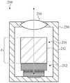
光学接近传感器110可以包括一个或多个VCSEL光源112、窗114和一个或多个光学路径延伸器116。广义地,光学接近传感器110可用于确定对象104的距离d和/或速度v。通过将光学路径长度延伸超出光学接近传感器110的视光学厚度,光学路径延伸器116可以减小该光学接近传感器的厚度。因此,光学接近传感器110占据电子设备102中的较少空间,和/或光学接近传感器可以放置在与传统光学接近传感器相比更小的、更薄的设备中,同时实现类似或改进的感测性能。相对于图2至图4B更详细地讨论示例性光学路径延伸器。
电源控制器122耦接到VCSEL光源112。这些部件中的每一个部件以及在特定实施方案或具体实施中可能需要或优选的光学接近传感器110的其他部件可以全部或部分地设置在部件壳体内。光学接近传感器110还包括窗114,该窗被配置为允许从VCSEL光源112发射的光穿过部件壳体以照射对象104的表面。在所示实施方案中,VCSEL光源112与窗114对准,使得从VCSEL光源112发射的光穿过窗114并且照射对象104的表面(其可以是用户、电子设备的内表面等)。The
在这些示例中,处理单元124可以被配置为使电源控制器122生成三角形电流波形(或其他合适的周期性或非周期性波形)以将电流注入VCSEL光源112中。为了简单起见,无论是通过调制还是以其他方式将电流注入到VCSEL光源中以发射光以及无论是通过如本文所述的电源控制器还是处理单元促进自混合的操作在本文中被称为“驱动”光源。In these examples, processing
来自对象104的反射穿过窗114并重新进入VCSEL光源112以引起与距离d直接相关的自混合干涉。在一些情况下,电源控制器122可以被进一步配置为监测来自光学耦合到VCSEL光源112的一个或多个光电二极管的功率输出,以便量化和/或以其他方式确定由自混合效应产生的VCSEL光源112的功率输出的变化(参见例如以下方程2和3)。The reflection from
光学接近传感器110可以具有在VCSEL光源112与目标104之间延伸的几何路径长度l。光学接近传感器110可具有相关联的光学路径长度(OPL),其等于几何路径长度l和光学接近传感器110的折射率的乘积。折射率可以沿着光学接近传感器110的几何路径长度l变化,在这种情况下,光学路径长度可以由方程1表示如下:
OPL=∫Cnds 方程1OPL=∫C nds
其中n为局部折射率作为沿几何路径C的距离的函数。where n is the local refractive index as a function of distance along the geometric path C.
光学路径长度与光穿过光学接近传感器110的几何路径的时间(即飞行时间)成比例。如上所述,光学路径延伸器116可以通过增加沿几何路径的介于VCSEL光源112和窗114之间的部分(图1中指示为l')的折射率来延伸光学接近传感器110的光学路径长度,而无需几何路径长度l的对应延伸。The optical path length is proportional to the time (ie, time of flight) for light to traverse the geometrical path of the
光学路径延伸器116可以以多种方式中的任何方式延伸光学接近传感器110的光学路径长度。在一些情况下,光学路径延伸器116可以是定位于VCSEL光源112与窗114之间的高折射率材料。在一些情况下,光学路径延伸器116可以与窗114集成在一起。在一些情况下,光学路径延伸器116可以与VCSEL光源112集成,例如作为底发射(倒装芯片)VCSEL光源的衬底,如关于图2更详细地讨论的。
光学路径延伸器116可以包括一个或多个重定向特征,该一个或多个重定向特征被配置为改变在VCSEL光源112与窗114之间行进的光的方向以创建折叠路径,如关于图3A至图3B更详细地讨论的。另外或替代地,光学路径延伸器116可以包括光子部件,该光子部件被配置为通过向行进通过其的光施加动量依赖性传递函数来模拟光学接近传感器内的几何路径的延伸,如关于图4A以及图4B更详细地讨论的。
如上所述,光学接近传感器110可用于确定到对象104的距离d和/或该对象的速度v。例如,在一个实施方案中,光学接近传感器110可以使用波长调制以同时检测到对象104的距离d和该对象相对于光学接近传感器110的速度v。波长调制可以通过调制供应到VCSEL光源112的驱动电流来实现。As mentioned above, the
一个示例性波长调制利用三角形波形,包括“向上循环”(其中向VCSEL光源112供应电流,并且相应地,从其发射的辐射光束的波长以特定速率线性地增加)和“向下循环”(其中向VCSEL光源112供应电流,并且从其发射的辐射光束的波长以相同的特定速率线性地减小)。在此示例中,波长的波动可以有效地模拟对象104朝向和远离光学接近传感器110的运动,无论该对象104实际上是否在移动。在这些示例中,来自VCSEL光源112的功率输出的频率含量—受自混合干涉效应影响—可以由方程2描述,在下文呈现。One exemplary wavelength modulation utilizes a triangular waveform, including "cycle up" (where current is supplied to the VCSEL
更具体地,在方程2(下文)中,参量ft表示由于在光学接近传感器110的VCSEL光源112在波长λ下发射光的特定时间t的自混合而调制来自光学接近传感器110的VCSEL光源112的功率输出的频率。参量ft可以表示基带频率或中频(IF),其通常比光学载波频率(波长)和其调制低几个数量级,并且易于由射频电子器件采样。More specifically, in Equation 2 (below), the parameter ft represents the modulation of the VCSEL
可以理解,由于到对象的绝对距离d改变(其等于总往返距离drt的一半),VCSEL光源112在时间t处接收的光与VCSEL光源112在相同的时间t发射的光相比将具有不同的波长,因为两个光束的波长相差与以下相关的量:波长随时间的变化率
以此方式,来自VCSEL光源112的功率输出遵循三角形波形(例如,电流以
更具体地,叠加干涉对应于在两个特定波长的光之间发生的相长干涉和相消干涉“模式”转换(例如,也称为拍频)的次数,该两个特定波长的光基于到对象的绝对距离(或者更具体地,行进到对象并返回所需的往返时间)并且基于波长的变化率

换种说法,在时间t0从VCSEL光源112发射的光的波长与在时间t1从VCSEL光源112发射的光的波长相差由波长的变化率

如此,通常且广泛地,可以理解,来自VCSEL光源112的功率输出的频率含量(例如,参量ft)与分离VCSEL光源112和对象104的OPL直接相关。As such, generally and broadly, it can be understood that the frequency content (eg, the parameter ft ) of the power output from the VCSEL
进一步地,可以理解,参量ft由于对象104的速度v产生的一个或多个多普勒效应可以增大或减小。例如,如果对象104正朝向光学接近传感器移动(例如,平行于发射光束的传播方向),则频率ft可以增大。可替代地,如果对象104正远离光学接近传感器(例如,平行于发射光束的传播方向)移动,则频率ft可以减小。Further, it will be appreciated that one or more Doppler effects of the parameter ft due to the velocityv of the
方程2,关于上文提及的值,如下:Equation 2, with respect to the values mentioned above, is as follows:

以更一般的形式,还可以考虑对象104的运动方向(或更具体地,对象104相对于发射光束的传播方向的运动角度θ)。方程3,表示这种更一般的形式,如下:In a more general form, the direction of movement of the object 104 (or more specifically, the angle of movement θ of the

使用方程2或方程3,可以理解,由
本文提出的实施方案,方程3中的drt可以增加相似或更薄的光学深度t,这导致所测量的ft朝向较高的射频移动。除了更薄的设备形状因子之外,移动ft远离主导低频本底噪声(例如,低频驱动器、激光器和检测器噪声和/或非线性残留)还使能更高的检测信噪比、更宽的空间感测范围和更好的空间感测准确度。For the implementation presented herein, drt in Equation 3 can be increased by a similar or thinner optical depth t, which results in a shift of the measured ft towards higher radio frequencies. In addition to thinner device form factors, movingft away from the dominant low-frequency noise floor (eg, low-frequency driver, laser and detector noise and/or nonlinear residuals) also enables higher detection signal-to-noise ratios, wider The highest spatial sensing range and better spatial sensing accuracy.
在许多实施方案中,光学接近传感器110被配置为利用三角形波形调制来从VCSEL光源(或VCSEL阵列)获得距离和速度信息两者,但是可以理解,这仅仅是一个示例并且可以使用其他构造和调制技术。In many embodiments, the
VCSEL光源112可以是形成于衬底或半导体管芯上的VCSEL光源;为了简化说明和描述,所示实施方案省略了这些元件中的许多,这些元件参考本文呈现的其他附图更详细地描述。在许多情况下,VCSEL光源112设置在保护壳体、灌封或封装(包括电子设备102的任何外壳或壳体)内以防止损坏。VCSEL
光学接近传感器110的VCSEL光源112可以形成为图案或阵列,尽管这可能不需要。光学接近传感器110的VCSEL光源112可以由任何数量的合适材料或材料组合形成。在一个示例性实施方案中,光学接近传感器110的VCSEL光源112各自包括但不限于或表达要求:第一分布式布拉格反射器层;限定发射孔的氧化物层;多量子阱结构;第二分布式布拉格反射器层;等等。在其他示例中,可能需要附加或更少层。The VCSEL
任何固定式或便携式电子设备可并入诸如本文所述的光学接近传感器。示例性电子设备包括但不限于:移动电话设备;平板设备;膝上型电脑设备;台式计算机;计算附件;外围输入设备;家用或商用联网设备;航空、航海、水下或陆地车辆控制设备或联网设备;移动娱乐设备;增强现实设备;虚拟现实设备;工业控制设备;数字钱包设备;家用或商用安全设备;可穿戴设备;头戴式设备;手持式控制器;健康或医疗设备;植入式设备;嵌入衣物的设备;时尚配饰设备;家用或工业电器;媒体设备;等等。Any stationary or portable electronic device can incorporate optical proximity sensors such as those described herein. Exemplary electronic devices include, but are not limited to: mobile phone devices; tablet devices; laptop devices; desktop computers; computing accessories; peripheral input devices; home or business networking devices; aviation, marine, underwater, or land vehicle control devices or Connected Devices; Mobile Entertainment Devices; Augmented Reality Devices; Virtual Reality Devices; Industrial Control Devices; Digital Wallet Devices; Home or Business Security Devices; Wearable Devices; Head-mounted Devices; Handheld Controllers; Health or Medical Devices; Implants fashion devices; devices embedded in clothing; fashion accessory devices; household or industrial appliances; media devices; and more.
类似地,光学接近传感器110可由电子设备用于多种合适的目的。示例性目的包括但不限于:检测用户的手指(或其他对象,如触笔)到电子设备的输入表面或部件的距离和速度;检测用户身体(或任何其他对象)到电子设备的输入表面或部件的距离和速度;检测由于(例如,由用户或其他对象,如触笔)施加力引起的变形而导致的电子设备的外壳的表面的挠曲;等等。Similarly,
类似地,光学接近传感器110可以包括任何数量的合适的光学路径延伸器、透镜或束成形元件。示例包括但不限于:反射器;反射镜;半透明透镜窗;透明透镜窗;凹透镜;凸透镜;倾斜透镜;微透镜;宏透镜;准直器;偏光器;滤色器;红外截止滤光器;红外带通滤光器;光纤电缆;等等。Similarly,
在许多实施方案中,光学接近传感器110包括由塑料或丙烯酸材料形成的部件壳体;包括玻璃和金属的其他导电或非导电/隔热材料也可以是合适的。部件壳体可以由单个材料形成,或者替代地,可以由以合适的方式(例如,通过粘合剂、焊接等)接合在一起的多个不同材料层或区域形成。In many embodiments, the
光学接近传感器110的部件壳体可以是不透明的或透明的,或者可以包括透明区域和不透明区域。部件壳体可以包括一个或多个反射区或区域。The component housing of the
在许多实施方案中,部件壳体包括设置在通过部件壳体限定的孔中或形成在部件壳体内的透镜114或窗。通常,透镜或窗设置在VCSEL光源112的正上方并与该VCSEL光源对准。由于这种构造,从VCSEL光源112发射/辐射的光束可从光学接近传感器110的部件壳体向外传播。作为这种构造的另外的结果,可以由VCSEL光源112接收可以从对象104的表面反射的发射/辐射光束的一个或多个反射。In many embodiments, the component housing includes a
在许多实施方案中,光学接近传感器110还包括与VCSEL光源112相邻设置或集成在该VCSEL光源中的一个或多个光电二极管。在这些示例中,光学接近传感器110(或更具体地,光学接近传感器110的或可通信地耦合到该光学接近传感器的电路或处理器)可以监测来自光电二极管的功率输出以确定一个或多个性能特性,诸如VCSEL光源112的该功率输出的拍频(参见例如,方程2和3)。然而,可以理解,此前述示例仅仅是一个示例;通过VCSEL光源和/或VCSEL光源的功耗监测和/或测量功率输出可以多种合适的方式执行。In many embodiments, the
与本文所述的其他实施方案一样,VCSEL光源112可以被配置为从光学接近传感器110的部件壳体向外发射激光光束。在所示实施方案中,VCSEL光源112被定向成在大致垂直于电子设备102的外壳的边缘的方向上发射/辐射光。然而,可以理解的是,这仅仅是一个示例,并且其他发射或辐射方向是可能的或甚至优选的(例如,确定在设备外壳的边缘外侧的目标速度)。As with the other embodiments described herein, the VCSEL
与本文所述的其他实施方案一样,VCSEL光源112被进一步配置为接收发射/辐射光束离开对象104的反射。这种反射可以导致VCSEL光源112内的自混合干涉,这又可以影响VCSEL光源112的功率输出。因此,监测VCSEL光源112的功率输出(例如,通过监测光电二极管的输出,如上文所描述)可用于确定和/或计算所述对象104沿着所述发射光束的所述光轴的距离d和速度v。(参见例如,方程2和3)。As with the other embodiments described herein, the VCSEL
光学接近传感器110和电子设备102可以以任何合适的方式可通信地或功能性地耦合。更具体地,根据符合任何合适的数字或模拟形式或格式的任何协议,光学接近传感器110可以被配置为以任何合适的方式向电子设备102的处理器或系统传送距离和/或速度信息(其基于VCSEL光源112的自混合来计算或以其他方式确定)。
此外,如上所述,电子设备102可以是包括固定和便携式电子设备的任何合适的电子设备。在一个实施方案中,电子设备102为可穿戴电子设备,诸如智能手表。在此示例中,电子设备102可利用光学接近传感器110来确定到用户(由对象104表示)的距离以及当用户与电子设备102交互时该用户的速度。例如,电子设备102可以利用从光学接近传感器110发送的信号来确定用户是否正穿戴智能手表或正将智能手表转向用户的面部。Furthermore, as noted above,
更具体地,在一些实施方案中,电子设备102可以被配置为在确定用户必须跨过一个或多个阈值(诸如距离阈值或速度阈值)时执行功能。此类阈值可以是可变的或固定的,并且可以由电子设备102的存储器设置和/或存储在所述存储器内。在一些示例中,阈值可以基于用户设置、应用程序设置或操作系统设置或操作模式。在其他情况下,此类阈值可以至少部分地基于由电子设备102的处理器执行或示例化的特定应用。例如,与电话应用程序相关联的阈值集可以不同于与游戏应用程序相关联的阈值集。可以理解,以任何合适的形式或格式存储或访问的任何合适的阈值或阈值集可以用于响应于从光学接近传感器110接收到的信号来通知电子设备102的一个或多个行为。More specifically, in some embodiments, the
在一个具体实施方案中,电子设备102可在确定用户距离电子设备102较远时禁用电子设备102的屏幕。In a specific embodiment, the
在另一具体实施方案中,电子设备102可以基于用户的距离和速度来修改电子设备102的显示器或功率设置。示例包括但可不限于:在从光学接近传感器110接收到用户在覆盖显示器的信号时,降低显示器或显示区域的亮度;在从光学接近传感器110接收到用户在覆盖显示器的信号时增加显示器的亮度;在从光学接近传感器110接收到用户将手指悬停在显示器附近的信号时,突出显示图形用户界面的用户界面元素(例如,列表的项、按钮等);在从光学接近传感器110接收到用户将手指悬停在电子设备102的输入部件(例如,旋转输入设备、按钮输入设备、触摸输入设备等)附近的信号时,突出显示或以其他方式修改图形用户界面的用户界面元素;等等。In another specific embodiment, the
在另一实施方案中,电子设备102可利用从光学接近传感器110接收的干涉测量信号来监测和/或认证用户的生物信息(例如,用户心率模式、血压、呼吸、咀嚼、说话、手势和移动等)。在另一实施方案中,电子设备102可利用从光学接近传感器110接收的干涉测量信号来测量目标特性,包括但不限于微粒、颗粒计数、表面纹理、次表面纹理等。In another embodiment, the
在另一实施方案中,电子设备102可以是便携式电子设备,诸如蜂窝电话。在这些示例中,电子设备102可以利用从光学接近传感器110接收的速度或距离信号来确定当电子设备的用户将蜂窝电话升高到用户耳朵时禁用或启用电子设备102的触敏显示器的适当时间。In another embodiment, the
在另一个实施方案中,电子设备102可利用从光学接近传感器110接收的速度或距离信号来确定电子设备102是否正在坠落或即将撞击表面。In another embodiment, the
在另一个实施方案中,电子设备102可以是车辆附件或附接件。在这些示例中,电子设备102可利用从光学接近传感器110接收的速度或距离信号来确定到另一车辆、行人或道路危险的距离和/或另一车辆、行人或道路危险的速度。In another embodiment, the
在另一实施方案中,电子设备102可以将光学接近传感器诸如光学接近传感器110定位在电子设备102的输入/输出通信端口或电源端口内。在这些示例中,电子设备102可以利用从光学接近传感器110接收的速度或距离信号来确定电缆是否正确地坐置在端口中、电缆是否太快或以可能导致对电子设备102造成损坏的方式移除,等等。In another embodiment,
可以理解,前述示例性实施方案不是穷举性的,并且如本文所述的光学接近传感器可以以任何合适的方式由电子设备用来确定已知或未知对象或表面相对于电子设备的距离和/或速度。It is to be understood that the foregoing exemplary embodiments are not exhaustive and that optical proximity sensors as described herein may be used by an electronic device in any suitable manner to determine the distance and/or distance of a known or unknown object or surface relative to the electronic device or speed.
例如,在一些实施方案中,电子设备可以包括多于一个光学接近传感器,如本文所述。在另一示例中,电子设备可以包括以图案布置的光学接近传感器阵列,诸如排成一行。For example, in some embodiments, an electronic device may include more than one optical proximity sensor, as described herein. In another example, an electronic device may include an array of optical proximity sensors arranged in a pattern, such as in a row.
在许多情况下,如本文所描述的光学接近传感器可以设置在电子设备的外壳内并且与由外壳限定的透明孔对准,但是这可能不是必需的。例如,在一些实施方案中,光学接近传感器可以设置在显示器后面。在其他情况下,光学接近传感器可以完全设置在电子设备外壳内。在这些示例中,光学接近传感器可以用于检测电子设备的表面中的挠曲或变形,所述挠曲或变形可来自用户有目的地向该表面施加力。例如,在一个实施方案中,光学接近传感器完全定位在电子设备的外壳内,位于显示器后面。在此示例中,当电子设备的用户向显示器施加力时,显示器可以变形或弯曲,从而缩短显示器与光学接近传感器之间的距离。光学接近传感器继而可以检测和测量此挠曲,电子设备的处理器(和/或光学接近传感器的处理器)可以将所述挠曲与力输入的量值相关。In many cases, an optical proximity sensor as described herein may be disposed within a housing of an electronic device and aligned with a transparent aperture defined by the housing, although this may not be required. For example, in some embodiments, an optical proximity sensor may be positioned behind the display. In other cases, the optical proximity sensor may be located entirely within the electronics housing. In these examples, an optical proximity sensor can be used to detect deflection or deformation in a surface of an electronic device, which can result from a user purposely applying a force to the surface. For example, in one embodiment, the optical proximity sensor is positioned entirely within the housing of the electronic device, behind the display. In this example, when a user of the electronic device applies force to the display, the display can deform or bend, thereby reducing the distance between the display and the optical proximity sensor. The optical proximity sensor can then detect and measure this deflection, which the processor of the electronic device (and/or the optical proximity sensor's processor) can correlate to the magnitude of the force input.
如本文所述,本文所讨论的光学路径延伸器可以以多种方式中的任何方式延伸光学接近传感器的光学路径长度。在一些情况下,光学路径延伸器可以是高折射率材料。图2示出了具有与VCSEL光源212集成的光学路径延伸器216的示例性光学接近传感器210。光学接近传感器210可以类似于本文讨论的光学接近传感器(例如,光学接近传感器110),并且可以具有类似的结构和/或功能,包括VCSEL光源212、窗214和壳体230。光学接近传感器210可以包括光学路径延伸器216,该光学路径延伸器被配置为使光学路径延伸穿过光学接近传感器。光学路径延伸器216可以是包括高折射率材料的衬底。合适的高折射率材料的示例包括砷化镓、氮化镓、玻璃、聚合物、化学涂层等。As described herein, the optical path extenders discussed herein can extend the optical path length of an optical proximity sensor in any of a variety of ways. In some cases, the optical path extender may be a high refractive index material. FIG. 2 shows an exemplary
在一些情况下,光学路径延伸器216可以是VCSEL光源212的衬底或另一部件。在图2所示的实施方案中,VCSEL光源212是倒装芯片VCSEL,这意味着光向上击发通过其上形成VCSEL芯片的衬底232。衬底232可以由高折射率材料形成,诸如砷化镓,使得衬底232形成光学路径延伸器216的至少一部分。In some cases, the
在许多传统的倒装芯片VCSEL中,在制造之后,此衬底被变薄(例如,到0.4mm、0.1mm或更小)以减小芯片的厚度。在图2的实施方案中,衬底232被设计成在VCSEL波长下在厚度上具有最小的光损耗,并且不会变薄或与传统的VCSEL相比变薄得更少。这可以通过增加光学接近传感器210的几何路径的比例来进一步延伸光学接近传感器的光学路径长度,光在该几何路径中行进穿过光学路径延伸器216的高折射率材料。在一些情况下,衬底232具有介于0.25mm与2mm之间、0.4mm与1mm之间、0.6mm与0.8mm之间等的厚度t。衬底232的折射率可在1.5与4.5之间、3与4之间、3.2与4.8之间等。因此,光学路径长度可以在衬底232的厚度的2.5倍与5倍之间、在衬底232的厚度的3倍与4.5倍之间等。In many conventional flip-chip VCSELs, after fabrication, this substrate is thinned (eg, to 0.4 mm, 0.1 mm, or less) to reduce the thickness of the chip. In the embodiment of FIG. 2, the
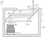
如上所述,本文所讨论的光学路径延伸器可以包括一个或多个重定向特征,所述一个或多个重定向特征被配置为改变沿光学接近传感器的光学路径行进的光的方向。图3A和图3B示出了示例性光学接近传感器310a、310b,其包括重定向特征以增加光学接近传感器的光学路径长度。光学接近传感器310a、310b可以类似于本文讨论的光学接近传感器(例如,光学接近传感器110、210),并且可以具有类似的结构和/或功能,包括VCSEL光源312、窗314、光学路径延伸器316a、316b和壳体330。As noted above, the optical path extenders discussed herein may include one or more redirecting features configured to change the direction of light traveling along the optical path of the optical proximity sensor. 3A and 3B illustrate exemplary
转向图3A,光学路径延伸器316a可以限定延伸穿过光学路径延伸器的光学路径334a。如图3A所示,光学路径334a的长度可以显著长于光学路径延伸器316a的厚度t,由此产生通过光学路径延伸器的大于厚度t的光学路径长度。如上所述,光学路径长度可以在厚度t的2.5倍与5倍之间、厚度t的3倍与4.5倍之间等。Turning to Figure 3A, the
如上所述,光学路径延伸器316a可以包括重定向特征,以在光学路径334a延伸穿过光学路径延伸器316a时改变该光学路径的方向一次或多次。例如,在图3A中,光学路径334a改变两次方向。光学路径延伸器316a可以包括反射镜340a、340b或其他合适的重定向特征以改变光学路径的方向。光学路径延伸器316a可以包括另外的光学特征,诸如光学特征342a、342b,以将光引导到光学路径延伸器316a之中和之外。光学特征342a、342b可以包括准直器、透镜等。在各种实施方案中,反射镜340a、340b不需要为平坦的和/或彼此平行,如图3A所示。这种定向自由可以使附加光束指向和成形功能超出光学路径延伸器的功能。As mentioned above, the
穿过光学路径延伸器316a的光学路径334a改变两次方向,但在各种实施方案中,光学路径可改变任何次数的方向。转到图3B,光学路径延伸器316b可以限定穿过光学路径延伸器的光学路径334b。类似于光学路径334a,光学路径334b的长度可以显著长于光学路径延伸器316b的厚度t,由此产生通过光学路径延伸器的大于厚度t的光学路径长度。在一些情况下,通过光学路径延伸器316b的光的重定向可以由于来自光学路径延伸器316b的表面的全内反射(或近全内反射)而发生。The optical path 334a passing through the
在一些情况下,光学路径延伸器316a、316b可以另外或替代地包括高折射率材料,包括玻璃、聚合物、化学涂层等,以进一步增加通过光学路径延伸器的光学路径长度。光学路径延伸器316a、316b的重定向特征和光学特征可以包括任何合适的光学路径延伸器、透镜或束成形元件。示例包括但不限于:反射器;反射镜;半透明透镜窗;透明透镜窗;凹透镜;凸透镜;倾斜透镜;微透镜;宏透镜;准直器;偏光器;滤色器;红外截止滤光器;红外带通滤光器;光纤电缆;等等。可以选择或设计用于本文所述的光学路径延伸器的材料以获得高通量、低扩散或雾化、低色散和/或其他光学、机械和/或化学特性,以有利于干涉测量传感。In some cases, the
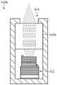
如上所述,本文所讨论的光学路径延伸器可以包括光子部件,所述光子部件被配置为模拟光学接近传感器内的几何路径的延伸。图4A和图4B示出了示例性光学接近传感器410a、410b,其包括光子部件416a、416b以增加光学接近传感器的光学路径长度。光学接近传感器410a、410b可以类似于本文讨论的光学接近传感器(例如,光学接近传感器110、210、310a、310b),并且可以具有类似的结构和/或功能,包括VCSEL光源412、窗414和壳体430。As noted above, the optical path extenders discussed herein may include photonic components configured to simulate the extension of geometric paths within an optical proximity sensor. 4A and 4B illustrate exemplary
光子部件416a、416b可以定位在VCSEL光源412和窗414之间,并且可以被配置为将传递函数施加到穿过光子部件的光以有效地将光传播比光子部件的厚度长得多的长度。在一些情况下,每个光子部件416a、416b将动量依赖性传递函数施加到穿过其的光。光子部件416a、416b可以再现傅立叶传递函数,其描述光通过具有比光子部件的厚度更长的光学路径长度的不同介质传播。光子部件416a、416b可以保持光的传播角度,使得离开光子部件416a、416b的光线平行于其对应的入射光线。The
在各种实施方案中,光子部件416a、416b可以以多种方式实施。在一些情况下,如图4A所示,光子部件416a可以是折射率小于或等于背景介质的折射率的平面平行板。在一些情况下,光子部件416a包括单轴光子晶体板,诸如方解石晶体,其轴线垂直于其入口面和出口面定向。在一些情况下,如图4B所示,光子部件416b是包括具有不同厚度的多层的超材料。超材料可以包括由硅和二氧化硅形成的交替层。In various embodiments, the
前述示例不是穷举性的;可以理解,大体上和广泛地,电子设备可以利用一个或多个光学接近传感器,如本文所述,用于任何合适的目的或功能。例如,图5A描绘了被配置为测量到对象504的距离d和/或对象504相对于如本文所述的光学接近传感器510的速度的电子设备502的示意图500a。在此示例性实施方案中,光学接近传感器510可以包括束成形透镜,该束成形透镜将从光学接近传感器510发射的光重定向成角度θ。以此方式并且由于这种构造,电子设备502和光学接近传感器510可以确定在多个方向上或沿着多个轴线的速度(例如,vx和vy)。以此方式,(任选地)与一个或多个附加光学接近传感器一起,电子设备502可以确定多轴速度和距离。The foregoing examples are not exhaustive; it is to be understood that, generally and broadly, electronic devices may utilize one or more optical proximity sensors, as described herein, for any suitable purpose or function. For example, FIG. 5A depicts a schematic 500a of an
其他实施方案可以其他方式实现。例如,图5B描绘了被配置为利用光学接近传感器510来测量到柔性表面508的距离d和该柔性表面508的一个或多个变形或弯曲的速度v的电子设备502的示意图500b。以此方式,并且由于这种构造,可以通过电子设备502来量化柔性表面508的弯曲。Other embodiments can be implemented in other ways. For example, FIG. 5B depicts a schematic 500b of an
在这些和相关示例上扩展,呈现图6A至图6D以描绘光学接近传感器的各种示例用例,如本文所述。这些图描绘了可穿戴电子设备,诸如智能手表,但是可以理解,这仅仅是一个示例。如本文所述,光学接近传感器可以并入到任何合适的电子设备中并且用于任何合适的目的。Expanding on these and related examples, FIGS. 6A-6D are presented to depict various example use cases for optical proximity sensors, as described herein. The figures depict a wearable electronic device, such as a smart watch, but it is understood that this is just an example. As described herein, optical proximity sensors may be incorporated into any suitable electronic device and used for any suitable purpose.
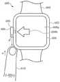
例如,图6A描绘了包括外壳602的可由用户(例如,经由腕带604)穿戴的可穿戴电子设备600。在此示例中,光学接近传感器606可以包括在外壳602内并且相对于显示器608的外围或边框区域定位,该外围或边框区域限定用户可与之交互的图形用户界面608a。由于这种构造,光学接近传感器606可以被配置为并定向成检测、测量或以其他方式确定用户的手指610相对于输入部件612的距离d和/或速度v。输入部件612可以是任何合适的输入部件,包括但不限于:旋转输入部件(例如,冠部);按钮输入部件;固态输入部件;等等。For example, FIG. 6A depicts a wearable
在此示例性实施方案中,可穿戴电子设备600可以被配置为在确定用户的手指610正接近输入部件612时执行第一功能,在确定用户的手指610正离开或移动远离输入部件612时执行第二功能,在确定用户的手指610正悬停在输入部件612附近或之上时执行第三功能,等等。可以理解,这些示例不是穷举性的并且可穿戴电子设备600可以基于如由光学接近传感器确定的用户的手指610相对于输入部件612的距离d和/或速度v执行任何合适的功能或操作。In this exemplary embodiment, the wearable
例如,在一个实施方案中,可穿戴电子设备600可以响应于输入部件612与用户的手指610之间的距离d的变化而修改图形用户界面元素608b的位置、特性、大小、颜色或其他性质。For example, in one embodiment, wearable
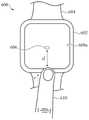
在另一示例中,图6B描绘了包括外壳602的被配置为经由腕带604耦接到用户的可穿戴电子设备600。如本文所述,光学接近传感器606可以设置在显示器608后面,所述显示器呈现图形用户界面608a。在一个示例中,光学接近传感器606被配置为通过显示器608的像素间区域发射光。In another example, FIG. 6B depicts a wearable
在此示例中,光学接近传感器606可被配置为并定向成检测、测量或以其他方式确定用户的手指610相对于显示器608和/或图形用户界面608a的距离d和/或速度v。显示器608可以被实施为或具有但不限于:触敏屏幕或显示器;力敏屏幕或显示器;触觉输出表面;等等。In this example,
在该示例性实施方案中,与本文描述的其他实施方案一样,可穿戴电子设备600可以被配置为基于如通过光学接近传感器确定的用户的手指610相对于显示器608的距离d和/或速度v(和/或其中随时间的变化)执行任何合适的功能或操作。In this exemplary embodiment, as with other embodiments described herein, wearable
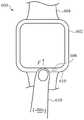
在另一示例中,图6C描绘了包括外壳602的可以经由腕带604附接到用户的可穿戴电子设备600。如本文所述,光学接近传感器可以设置在外壳602内。在此示例中,光学接近传感器可以被配置为并定向成检测、测量或以其他方式确定由用户的手指610施加到由显示器608呈现的图形用户界面608a的向下的力产生的显示器608的挠曲的距离d和/或速度d。显示器608可以以与参考图6B所述相同的方式配置,并且此描述不再重复。In another example, FIG. 6C depicts a wearable
在该示例性实施方案中,与本文描述的其他实施方案一样,可穿戴电子设备600可以被配置为基于如通过光学接近传感器确定的用户的手指610相对于显示器608的距离d和/或速度v(和/或其中随时间的变化)执行任何合适的功能或操作。在许多示例中,可穿戴电子设备600可以被配置为将显示器608的挠曲的距离d和/或速度v中的至少一者关联或以其他方式转换成力输入的量值F。In this exemplary embodiment, as with other embodiments described herein, wearable
在又一示例中,图6D描绘了包括外壳602的可以经由腕带604附接到用户的可穿戴电子设备600。如本文所述,光学接近传感器606可以设置在外壳602内,邻近外壳602的侧壁。更具体地,在此示例中,光学接近传感器606可被配置为并定向成检测、测量或以其他方式确定由用户施加的力F引起的外壳侧壁或外壳部分的挠曲的距离d和/或速度v。In yet another example, FIG. 6D depicts a wearable
在此示例性实施方案中,与本文所述的其他实施方案一样,可穿戴电子设备600可以被配置为基于如由光学接近传感器确定的用户的手指610施加的所述力F的确定量值(和/或其中随时间的变化)执行任何合适的功能或操作。In this exemplary embodiment, as with other embodiments described herein, wearable
图1至图6B中描绘的前述实施方案以及其各种另选方案和其变型通常出于解释的目的并且为了促进理解诸如本文所述的光学接近传感器的各种可能构造而呈现。然而,对于本领域的技术人员而言将显而易见的是,本文所呈现的具体细节中的一些细节可为实践特定的所述实施方案或其等同物所不需要的。The foregoing embodiments depicted in FIGS. 1-6B, as well as various alternatives and variations thereof, are presented generally for purposes of explanation and to facilitate understanding of the various possible configurations of optical proximity sensors such as those described herein. However, it will be apparent to those skilled in the art that some of the specific details presented herein may not be required to practice particular described embodiments or their equivalents.
图7为描绘了诸如本文所述的用于操作接近传感器的一种方法700的示例性操作的流程图。方法700包括操作702,其中监测(例如,如本文所述光学耦合到VCSEL的光电二极管的)输出信号的频率含量。接下来,在操作704处,可以基于操作702的监测到的频率含量来确定距离和/或速度信息。7 is a flowchart depicting exemplary operations of a
图8示出了可以执行本文所述的操作的电子设备800的样本电气框图。在一些情况下,电子设备800可以采取参考图1至图7描述的任何电子设备的形式,包括电子设备102、502和602和/或光学接近传感器110、210、310、410、510和610。电子设备800可以包括显示器812、处理单元802、电源814、存储器804或存储设备、输入设备806和输出设备810中的一者或多者。在一些情况下,电子设备800的各种具体实施可以缺乏这些部件中的一些或全部和/或包括附加或替代部件。FIG. 8 shows a sample electrical block diagram of an
处理单元802可以控制电子设备800的一些或所有操作。处理单元802可以直接或间接地与电子设备800的一些或所有部件通信。例如,系统总线或其他通信机构816可以提供处理单元802、电源814、存储器804、输入设备806和输出设备810之间的通信。
处理单元802可以被实现为能够处理、接收或传输数据或指令的任何电子设备。例如,处理单元802可以是微处理器、中央处理单元(CPU)、专用集成电路(ASIC)、数字信号处理器(DSP)或此类设备的组合。如本文所述,术语“处理单元”意在涵盖单个处理器或处理单元、多个处理器、多个处理单元或其他适当配置的一个或多个计算元件。
应当指出的是,电子设备800的部件可以由多个处理单元控制。例如,电子设备800的选择部件(例如,输入设备806)可以由第一处理单元控制,并且电子设备800的其他部件(例如,显示器812)可以由第二处理单元控制,其中第一处理单元和第二处理单元可以彼此通信,也可以不彼此通信。It should be noted that components of
电源814可以用能够向电子设备800提供能量的任何设备来实现。例如,电源814可以是一个或多个电池或者可再充电电池。附加地或另选地,电源814可以是将电子设备800连接到另一电源(诸如壁装电源插座)的电源连接器或电源线。
存储器804可以存储可以由电子设备800使用的电子数据。例如,存储器804可以存储电子数据或内容,诸如例如音频文件和视频文件、文档和应用程序、设备设置和用户偏好、定时信号、控制信号以及数据结构或数据库。存储器804可以被配置为任何类型的存储器。仅以举例的方式,存储器804可以被实现为随机存取存储器、只读存储器、闪存存储器、可移动存储器、其他类型的存储元件或此类设备的组合。
在各种实施方案中,显示器812提供例如与电子设备800的操作系统、用户界面和/或应用(例如,聊天用户界面、问题跟踪用户界面、问题发现用户界面等)相关联的图形输出。在一个实施方案中,显示器812包括一个或多个传感器并且被配置为触敏显示器(例如,单点触摸、多点触摸)和/或力敏显示器以接收来自用户的输入。例如,显示器812可以与触摸传感器(例如,电容式触摸传感器)和/或力传感器集成,以提供触敏显示器和/或力敏显示器。显示器812可操作地耦接到电子设备800的处理单元802。In various embodiments,
显示器812可以用任何合适的技术来实现,该技术包括但不限于液晶显示器(LCD)技术、发光二极管(LED)技术、有机发光显示器(OLED)技术、有机电致发光(OEL)技术,或另一类型的显示器技术。在一些情况下,显示器812定位在形成电子设备800的壳体的至少一部分的覆盖件下方并且能够透过该覆盖件看见。
在各种实施方案中,输入设备806可以包括用于检测输入的任何合适的部件。输入设备806的示例包括光传感器、温度传感器、音频传感器(例如,麦克风)、光学或视觉传感器(例如,相机、可见光传感器或不可见光传感器)、接近传感器、触摸传感器、力传感器、机械设备(例如,冠部、开关、按钮或按键)、振动传感器、取向传感器、运动传感器(例如,加速度计或速度传感器)、位置传感器(例如,全球定位系统(GPS)设备)、热传感器、通信设备(例如,有线或无线通信设备)、电阻传感器、磁传感器、电活性聚合物(EAP)、应变仪、电极等,或它们的某种组合。每个输入设备806可以被配置为检测一个或多个特定类型的输入并且提供对应于检测到的输入的信号(例如,输入信号)。例如,可以将该信号提供给处理单元802。In various embodiments,
如上所讨论,在一些情况下,输入设备806包括与显示器812集成以提供触敏显示器的触摸传感器(例如,电容式触摸传感器)。类似地,在一些情况下,输入设备806包括与显示器812集成以提供力敏显示器的力传感器(例如,电容式力传感器)。As discussed above, in some cases,
输出设备810可以包括用于提供输出的任何合适的部件。输出设备810的示例包括光发射器、音频输出设备(例如,扬声器)、视觉输出设备(例如,灯或显示器)、触感输出设备(例如,触觉输出设备)、通信设备(例如,有线或无线通信设备)等或它们的某种组合。每个输出设备810可以被配置为接收一个或多个信号(例如,由处理单元802提供的输出信号)并且提供对应于该信号的输出。
在一些情况下,输入设备806和输出设备810一起实现为单个设备。例如,输入/输出设备或端口可经由通信网络诸如无线和/或有线网络连接传输电信号。无线和有线网络连接的示例包括但不限于蜂窝网络、Wi-Fi、蓝牙、IR和以太网连接。In some cases,
处理单元802可以可操作地耦接到输入设备806和输出设备810。处理单元802可以适于与输入设备806和输出设备810交换信号。例如,处理单元802可以从输入设备806接收对应于由输入设备806检测到的输入的输入信号。处理单元802可以解译所接收的输入信号,以确定是否响应于该输入信号提供和/或改变一个或多个输出。处理单元802随后可以向输出设备810中的一个或多个输出设备发送输出信号,以根据需要提供和/或改变输出。
如本文所用,在用术语“和”或“或”分开项目中任何项目的一系列项目之后的短语“中的至少一者”是将列表作为整体进行修饰,而不是修饰列表中的每个成员。短语“中的至少一者”不要求选择所列出的每个项目中的至少一个;相反,该短语允许包括项目中任何项目中的最少一者和/或项目的任何组合中的最少一者和/或项目中每个项目中的最少一者的含义。举例来说,短语“A、B和C中的至少一者”或“A、B或C中的至少一者”各自是指仅A、仅B或仅C;A、B和C的任意组合;和/或A、B和C中的每一者中的一者或多者。类似地,可以理解,针对本文提供的结合列表或分离列表而呈现的元素的顺序不应被解释为将本公开仅限于所提供的顺序。As used herein, the phrase "at least one of" after a series of items separating any of the items with the terms "and" or "or" modifies the list as a whole and not each member of the list . The phrase "at least one of" does not require selection of at least one of each item listed; rather, the phrase allows the inclusion of at least one of any of the items and/or at least one of any combination of items and/or the meaning of at least one of each item in the item. For example, the phrases "at least one of A, B, and C" or "at least one of A, B, or C" each mean only A, only B, or only C; any combination of A, B, and C ; and/or one or more of each of A, B, and C. Similarly, it is to be understood that the order of the elements presented with respect to the combined or separate lists provided herein should not be construed to limit the disclosure to the order presented.
可以理解的是,尽管上面公开了许多实施方案,但相对于本文所述的方法和技术所提供的操作和步骤旨在为示例性的并且因此不是穷举的。可以进一步理解的是,针对特定的实施方案可以要求或者期望另选的步骤顺序或者更少或附加的操作。It is to be understood that while many embodiments are disclosed above, the operations and steps presented with respect to the methods and techniques described herein are intended to be exemplary and therefore not exhaustive. It will be further understood that alternative sequences of steps or fewer or additional operations may be required or desired for a particular implementation.
尽管根据各种示例性实施方案和具体实施描述了上述公开,但应当理解,一个或多个单独实施方案中描述的各种特征、方面和功能不限于将它们应用于它们被描述的具体实施方案中,而是相反地它们可单独地或者以各种组合应用于本发明的一些实施方案中的一个或多个,而不论此类实施方案是否被描述以及此类特征是否作为所述实施方案的一部分被呈现。因此,本发明的广度和范围不应受任何上述示例性实施方案的限制,但相反地受本文所提供的权利要求书的限定。While the above disclosure has been described in terms of various exemplary embodiments and specific implementations, it should be understood that the various features, aspects and functions described in one or more separate embodiments are not limited in their application to the specific embodiments for which they are described , but rather they may be applied to one or more of some embodiments of the invention, alone or in various combinations, whether or not such embodiments are described and such features are part is presented. Thus, the breadth and scope of the present invention should not be limited by any of the above-described exemplary embodiments, but rather by the claims presented herein.
Claims (20)
Translated fromChineseApplications Claiming Priority (2)
| Application Number | Priority Date | Filing Date | Title |
|---|---|---|---|
| US17/167,218 | 2021-02-04 | ||
| US17/167,218US11629948B2 (en) | 2021-02-04 | 2021-02-04 | Optical interferometry proximity sensor with optical path extender |
Publications (1)
| Publication Number | Publication Date |
|---|---|
| CN114859367Atrue CN114859367A (en) | 2022-08-05 |
Family
ID=79730663
Family Applications (1)
| Application Number | Title | Priority Date | Filing Date |
|---|---|---|---|
| CN202210100812.8APendingCN114859367A (en) | 2021-02-04 | 2022-01-27 | Optical interferometric proximity sensor with optical path extender |
Country Status (5)
| Country | Link |
|---|---|
| US (1) | US11629948B2 (en) |
| EP (1) | EP4040102A1 (en) |
| JP (1) | JP2022119748A (en) |
| KR (1) | KR102693680B1 (en) |
| CN (1) | CN114859367A (en) |
Families Citing this family (8)
| Publication number | Priority date | Publication date | Assignee | Title |
|---|---|---|---|---|
| US11740071B2 (en) | 2018-12-21 | 2023-08-29 | Apple Inc. | Optical interferometry proximity sensor with temperature variation compensation |
| US11243068B1 (en) | 2019-02-28 | 2022-02-08 | Apple Inc. | Configuration and operation of array of self-mixing interferometry sensors |
| US11156456B2 (en) | 2019-05-21 | 2021-10-26 | Apple Inc. | Optical proximity sensor integrated into a camera module for an electronic device |
| US11473898B2 (en) | 2019-05-24 | 2022-10-18 | Apple Inc. | Wearable voice-induced vibration or silent gesture sensor |
| US11874110B2 (en) | 2020-09-25 | 2024-01-16 | Apple Inc. | Self-mixing interferometry device configured for non-reciprocal sensing |
| US12209890B2 (en) | 2022-03-31 | 2025-01-28 | Apple Inc. | Optical sensor module including an interferometric sensor and extended depth of focus optics |
| US12439167B1 (en)* | 2022-12-23 | 2025-10-07 | Ambarella International Lp | IR illumination control for cameras with multi-region array |
| DE102023111344A1 (en)* | 2023-05-03 | 2024-11-07 | Trumpf Photonic Components Gmbh | Method for measuring a topography of a welding area in a welding process and welding system |
Citations (9)
| Publication number | Priority date | Publication date | Assignee | Title |
|---|---|---|---|---|
| US20060158654A1 (en)* | 2005-01-18 | 2006-07-20 | Darfon Electronics Corp. | Optical detecting module and optical detector thereof |
| JP2009222573A (en)* | 2008-03-17 | 2009-10-01 | Toyota Central R&D Labs Inc | Distance measuring apparatus |
| US20120200858A1 (en)* | 2009-10-23 | 2012-08-09 | Koninklijke Philips Electronics, N.V. | Self-mixing interference device with wave guide structure |
| JP2014078823A (en)* | 2012-10-10 | 2014-05-01 | Nec Saitama Ltd | Portable electronic apparatus, and control method and program of the same |
| JP2019515258A (en)* | 2016-05-19 | 2019-06-06 | コーニンクレッカ フィリップス エヌ ヴェKoninklijke Philips N.V. | Small laser sensor |
| US20190317454A1 (en)* | 2018-04-13 | 2019-10-17 | Apple Inc. | Coherent Mixing Interference Based Sensors for Characterizing Movement of a Watch Crown |
| EP3598591A1 (en)* | 2018-07-17 | 2020-01-22 | Koninklijke Philips N.V. | Laser arrangement with reduced building height |
| US20200097124A1 (en)* | 2018-09-25 | 2020-03-26 | Apple Inc. | Waveguide-Based Interferometric Multi-Point/Distributed Force and Touch Sensors |
| US20200374620A1 (en)* | 2018-04-13 | 2020-11-26 | Apple Inc. | Self-Mixing Interference Based Sensors for Characterizing User Input |
Family Cites Families (117)
| Publication number | Priority date | Publication date | Assignee | Title |
|---|---|---|---|---|
| US4254333A (en) | 1978-05-31 | 1981-03-03 | Bergstroem Arne | Optoelectronic circuit element |
| US4468131A (en) | 1982-05-03 | 1984-08-28 | Asulab S.A. | Electronic watch having a non-moving means of control |
| US4913547A (en) | 1988-01-29 | 1990-04-03 | Moran Steven E | Optically phased-locked speckle pattern interferometer |
| FR2751755B1 (en) | 1996-07-23 | 1998-08-28 | Commissariat Energie Atomique | AUTODYNE DETECTION LASER VELOCIMETER |
| US5781297A (en) | 1996-08-23 | 1998-07-14 | M&M Precision Systems Corporation | Mixed frequency and amplitude modulated fiber optic heterodyne interferometer for distance measurement |
| US6233045B1 (en) | 1998-05-18 | 2001-05-15 | Light Works Llc | Self-mixing sensor apparatus and method |
| CN1227617C (en) | 2000-11-06 | 2005-11-16 | 皇家菲利浦电子有限公司 | Method of measuring movement of input device |
| US7667851B2 (en) | 2001-07-24 | 2010-02-23 | Lockheed Martin Corporation | Method and apparatus for using a two-wave mixing ultrasonic detection in rapid scanning applications |
| US6816523B1 (en) | 2001-08-27 | 2004-11-09 | Amkor Technology, Inc. | VCSEL package and fabrication method |
| US20050157971A1 (en) | 2002-05-17 | 2005-07-21 | Rene Juijve | Apparatus comprising an optical input device and at least one further optical device having a common radiation source |
| TWI313835B (en) | 2002-06-04 | 2009-08-21 | Koninkl Philips Electronics Nv | Method of measuring the movement of an object relative to a user's input device and related input device,mobile phone apparatus, cordless phone apparatus, laptor computer, mouse and remote control |
| GB0317858D0 (en) | 2003-07-30 | 2003-09-03 | Denselight Semiconductors Pte | Optical transceiver |
| US20050156874A1 (en) | 2004-01-21 | 2005-07-21 | Microsoft Corporation | Data input device and method for detecting life-off from a tracking surface by laser doppler self-mixing effects |
| JP4556481B2 (en) | 2004-05-14 | 2010-10-06 | 住友電気工業株式会社 | Optical transceiver |
| US7509050B2 (en) | 2004-06-30 | 2009-03-24 | Finisar Corporation | Microcode-driven self-calibration of optical transceivers to environmental conditions |
| US7277180B2 (en) | 2004-11-09 | 2007-10-02 | Zygo Corporation | Optical connection for interferometry |
| US7388672B2 (en) | 2004-11-19 | 2008-06-17 | Carl Ziess Meditec, Inc. | High efficiency balanced detection interferometer |
| WO2006069443A1 (en) | 2004-12-27 | 2006-07-06 | Bc Cancer Agency | Surface roughness measurement methods and apparatus |
| US7139446B2 (en) | 2005-02-17 | 2006-11-21 | Metris Usa Inc. | Compact fiber optic geometry for a counter-chirp FMCW coherent laser radar |
| US20060239312A1 (en) | 2005-04-23 | 2006-10-26 | Telaris Inc. | Semiconductor Lasers in Optical Phase-Locked Loops |
| US7557795B2 (en)* | 2005-06-30 | 2009-07-07 | Microsoft Corporation | Input device using laser self-mixing velocimeter |
| US7675020B2 (en) | 2006-08-28 | 2010-03-09 | Avago Technologies General Ip (Singapore) Pte. Ltd. | Input apparatus and methods having diffuse and specular tracking modes |
| US8208814B2 (en) | 2007-04-25 | 2012-06-26 | IPhotonixs, LLC | Optical transceiver calibration system and method |
| JP5685438B2 (en) | 2007-05-07 | 2015-03-18 | コーニンクレッカ フィリップス エヌ ヴェ | Laser sensor for self-mixing interferometer with wide detection range |
| JP2009008758A (en) | 2007-06-26 | 2009-01-15 | Fujinon Corp | Imaging device, camera module, and portable terminal device |
| US8378287B2 (en)* | 2007-06-27 | 2013-02-19 | Koninklijke Philips Electronics N.V. | Optical sensor module including a diode laser and a substrate transparent to radiation emitted by the diode laser and a method for manufacturing an optical sensor module |
| CN101796371A (en) | 2007-09-03 | 2010-08-04 | 皇家飞利浦电子股份有限公司 | Laser sensor based system for status detection of tires |
| EP2068212A1 (en) | 2007-12-06 | 2009-06-10 | The Swatch Group Research and Development Ltd. | Portable object such as a timepiece comprising means for triggering an electronic control function |
| WO2009113001A1 (en) | 2008-03-13 | 2009-09-17 | Philips Intellectual Property & Standards Gmbh | Sensor system, vehicle control system and driver information system for vehicle safety |
| US8564783B2 (en) | 2008-05-15 | 2013-10-22 | Axsun Technologies, Inc. | Optical coherence tomography laser with integrated clock |
| WO2009138912A2 (en) | 2008-05-16 | 2009-11-19 | Philips Intellectual Property & Standards Gmbh | Security system comprising a self-mixing laser sensor and method of driving such a security system |
| WO2009156937A1 (en) | 2008-06-27 | 2009-12-30 | Philips Intellectual Property & Standards Gmbh | Sensing apparatus for sensing a movement |
| CN102089617B (en) | 2008-07-07 | 2013-06-12 | 皇家飞利浦电子股份有限公司 | Laser self-mixing measurement system |
| US8446592B1 (en) | 2008-08-04 | 2013-05-21 | Stc.Unm | Scanning phase intracavity nanoscope |
| JP4600554B2 (en) | 2008-09-18 | 2010-12-15 | 富士ゼロックス株式会社 | Measuring device |
| JP5616009B2 (en) | 2008-09-22 | 2014-10-29 | アズビル株式会社 | Reflective photoelectric sensor and object detection method |
| JP2010160117A (en) | 2009-01-09 | 2010-07-22 | Fuji Xerox Co Ltd | Measuring device |
| EP2409115A2 (en)* | 2009-03-18 | 2012-01-25 | Koninklijke Philips Electronics N.V. | Apparatus for determining a flow property of a fluid |
| US8736581B2 (en) | 2009-06-01 | 2014-05-27 | Perceptive Pixel Inc. | Touch sensing with frustrated total internal reflection |
| CN101592762B (en) | 2009-06-05 | 2012-07-04 | 中兴通讯股份有限公司 | Optical module and control method thereof |
| WO2011012168A1 (en) | 2009-07-31 | 2011-02-03 | Lemoptix Sa | Optical micro-projection system and projection method |
| CN102109650B (en) | 2009-12-28 | 2014-02-19 | 鸿富锦精密工业(深圳)有限公司 | Preparation method of lens module |
| JP5368369B2 (en) | 2010-04-28 | 2013-12-18 | 株式会社デンソー | In-vehicle imaging device and in-vehicle image processing device |
| WO2012049561A1 (en) | 2010-10-15 | 2012-04-19 | Universitat Politècnica De Catalunya | A method of measuring a displacement-related parameter using a laser self-mixing measuring system, and a laser self-mixing measuring system |
| EP2520924A1 (en) | 2011-05-02 | 2012-11-07 | Axetris AG | Method and measurement assembly for improving signal resolution in gas absorption spectroscopy |
| CN103561637B (en) | 2011-06-01 | 2016-05-18 | 皇家飞利浦有限公司 | Determine the flow behavior of the object that can move in element |
| US9143703B2 (en) | 2011-06-10 | 2015-09-22 | Flir Systems, Inc. | Infrared camera calibration techniques |
| JP5903796B2 (en) | 2011-08-12 | 2016-04-13 | ソニー株式会社 | Imaging device and camera module |
| US9160390B2 (en) | 2011-10-07 | 2015-10-13 | Maxlinear, Inc. | Method and system for impairment shifting |
| GB201117480D0 (en)* | 2011-10-10 | 2011-11-23 | Palikaras George | Filter |
| JP5846872B2 (en) | 2011-11-21 | 2016-01-20 | 日立オートモティブシステムズ株式会社 | Image processing device |
| US9146304B2 (en) | 2012-09-10 | 2015-09-29 | Apple Inc. | Optical proximity sensor with ambient light and temperature compensation |
| US20150309568A1 (en) | 2012-11-27 | 2015-10-29 | Kyocera Corporation | Electronic apparatus and eye-gaze input method |
| KR102124832B1 (en) | 2013-04-03 | 2020-06-19 | 삼성전자주식회사 | Auto focus system of camera device, and camera device using the same |
| FR3008180B1 (en) | 2013-07-08 | 2016-11-25 | Inst Nat Polytechnique Toulouse | OPTICAL DEVICE FOR MEASURING A PHYSICAL PARAMETER AND ASSOCIATED METHOD |
| EP2860550B1 (en) | 2013-10-09 | 2016-03-02 | Hexagon Technology Center GmbH | Scanner for spatial measurement |
| JP2015078946A (en)* | 2013-10-18 | 2015-04-23 | 株式会社キーエンス | Distance measurement type photoelectric sensor and control method of projection light spot thereof |
| EP2887008A1 (en) | 2013-12-17 | 2015-06-24 | Universitat Politècnica de Catalunya | A method of measuring a change in an optical path using differential laser self-mixing interferometry and a differential laser self-mixing interferometry measuring system |
| US9772398B2 (en) | 2014-06-26 | 2017-09-26 | Intersil Americas LLC | Optical proximity sensors with reconfigurable photodiode array |
| JP2016014616A (en) | 2014-07-03 | 2016-01-28 | アズビル株式会社 | Velocity transition measuring device and velocity transition measuring method |
| DE202014103294U1 (en) | 2014-07-17 | 2015-10-21 | Ipek International Gmbh | Focusing system and camera unit with a focusing system |
| US9995877B2 (en) | 2014-09-22 | 2018-06-12 | Nec Corporation | Optical circuit element and configuration method for the optical circuit element |
| WO2016047523A1 (en) | 2014-09-26 | 2016-03-31 | 旭硝子株式会社 | Optical element and imaging device |
| US9459352B2 (en) | 2014-11-20 | 2016-10-04 | Texas Instruments Incorporated | Multi-sensor proximity sensing using a near zone light sensor and a far zone light sensor |
| CN107529983A (en) | 2015-01-09 | 2018-01-02 | 智能视觉实验室股份有限公司 | Portable wavefront analyzer with open field aligned with channel |
| US20180073924A1 (en) | 2015-03-19 | 2018-03-15 | Heptagon Micro Optics Pte. Ltd. | Optoelectronic module for spectral and proximity data acquisition |
| US10327069B2 (en) | 2015-07-26 | 2019-06-18 | Vocalzoom Systems Ltd. | Laser microphone utilizing speckles noise reduction |
| RU2716878C2 (en) | 2015-07-30 | 2020-03-17 | Конинклейке Филипс Н.В. | Laser sensor for detecting particle density |
| US10379028B2 (en) | 2015-07-30 | 2019-08-13 | Philips Photonics Gmbh | Laser sensor for multi parameter detection |
| US11036318B2 (en) | 2015-09-30 | 2021-06-15 | Apple Inc. | Capacitive touch or proximity detection for crown |
| EP3193192B1 (en) | 2016-01-12 | 2020-04-29 | ams AG | Optical sensor arrangement |
| CN205594581U (en) | 2016-04-06 | 2016-09-21 | 北京七鑫易维信息技术有限公司 | Module is tracked to eyeball of video glasses |
| US20170343810A1 (en) | 2016-05-24 | 2017-11-30 | Osterhout Group, Inc. | Pre-assembled solid optical assembly for head worn computers |
| US11300666B2 (en) | 2016-04-13 | 2022-04-12 | Oulun Yliopisto | Distance measuring device and transmitter, receiver and method thereof |
| JP2019522778A (en) | 2016-05-19 | 2019-08-15 | コーニンクレッカ フィリップス エヌ ヴェKoninklijke Philips N.V. | Particle sensor, particle detection method, and computer program |
| KR101728635B1 (en) | 2016-05-31 | 2017-04-20 | 연세대학교 산학협력단 | Apparatus and method for recognizing expression |
| US10718922B2 (en) | 2016-06-01 | 2020-07-21 | Ams Sensors Singapore Pte. Ltd. | Optoelectronic module including lens barrel comprising flanges and adhesive thereon and resting directly on a cover glass |
| US10635800B2 (en) | 2016-06-07 | 2020-04-28 | Vocalzoom Systems Ltd. | System, device, and method of voice-based user authentication utilizing a challenge |
| GB201611046D0 (en) | 2016-06-24 | 2016-08-10 | Npl Man Ltd | Optical resonator systems |
| US9911890B2 (en) | 2016-06-30 | 2018-03-06 | Stmicroelectronics Pte Ltd | Optical sensor package including a cavity formed in an image sensor die |
| CN206178658U (en) | 2016-08-10 | 2017-05-17 | 北京七鑫易维信息技术有限公司 | Module is tracked to eyeball of video glasses |
| DE102016215746A1 (en) | 2016-08-23 | 2018-03-01 | Robert Bosch Gmbh | Projector with non-contact control |
| US10215555B2 (en) | 2016-09-16 | 2019-02-26 | Apple Inc. | Motion sensing by monitoring intensity of light redirected by an intensity pattern |
| CN109716268B (en) | 2016-09-22 | 2022-05-17 | 苹果公司 | Eye and head tracking |
| EP3343894B1 (en) | 2016-12-28 | 2018-10-31 | Axis AB | Ir-filter arrangement |
| JP6988409B2 (en) | 2017-04-03 | 2022-01-05 | 株式会社デンソー | The camera module |
| EP3401666A1 (en) | 2017-05-11 | 2018-11-14 | Mettler-Toledo GmbH | Gas measurement system |
| EP3461292B1 (en) | 2017-07-18 | 2021-03-24 | Shenzhen Goodix Technology Co., Ltd. | Anti-spoofing sensing for rejecting fake fingerprint patterns in under-screen optical sensor module for on-screen fingerprint sensing |
| EP3451700A1 (en) | 2017-08-28 | 2019-03-06 | "BOCORE" GmbH | Device for reproducing an audio signal |
| US10791283B2 (en) | 2017-09-01 | 2020-09-29 | Facebook Technologies, Llc | Imaging device based on lens assembly with embedded filter |
| US10222474B1 (en) | 2017-12-13 | 2019-03-05 | Soraa Laser Diode, Inc. | Lidar systems including a gallium and nitrogen containing laser light source |
| JP2019121691A (en) | 2018-01-05 | 2019-07-22 | 富士通株式会社 | Integrated laser light source and optical transceiver using the same |
| CN108225543B (en) | 2018-03-28 | 2019-06-25 | 中国科学院长春光学精密机械与物理研究所 | A kind of the orthogonal detection vibration measurement device and method of self-mixed interference |
| EP3773137A4 (en) | 2018-03-30 | 2021-10-13 | Blaze Bioscience, Inc. | Systems and methods for simultaneous near-infrared light and visible light imaging |
| CN108692663B (en) | 2018-04-11 | 2020-04-21 | 南京师范大学 | Phase modulation type orthogonal polarization laser feedback grating interferometer and its measurement method |
| FR3080219B1 (en) | 2018-04-13 | 2021-03-05 | St Microelectronics Grenoble 2 | ELECTRONIC DEVICE INCLUDING ELECTRONIC CHIPS |
| US11157113B2 (en) | 2018-04-13 | 2021-10-26 | Apple Inc. | Self-mixing interference based sensors for characterizing touch input |
| US11360440B2 (en) | 2018-06-25 | 2022-06-14 | Apple Inc. | Crown for an electronic watch |
| EP3588700A1 (en)* | 2018-06-26 | 2020-01-01 | Koninklijke Philips N.V. | Vcsel device for an smi sensor for recording three-dimensional pictures |
| EP3588057A1 (en) | 2018-06-29 | 2020-01-01 | Koninklijke Philips N.V. | Method of reducing false-positive particle counts of an interference particle sensor module |
| US10871836B2 (en)* | 2018-07-06 | 2020-12-22 | Apple Inc. | System and method for unintentional input rejection |
| US11073615B2 (en) | 2018-08-20 | 2021-07-27 | Lite-On Singapore Pte. Ltd. | Proximity sensor module with two sensors |
| US11280714B2 (en) | 2018-08-21 | 2022-03-22 | Apple Inc. | Particulate matter velocity measurement and size estimation using parallel self-mixing sensing |
| US11092480B2 (en) | 2018-09-27 | 2021-08-17 | International Business Machines Corporation | Light obstruction sensor |
| EP3657672B1 (en) | 2018-11-21 | 2022-08-10 | Nxp B.V. | Wireless receivers and related methods with random interferer immunity |
| US11740071B2 (en) | 2018-12-21 | 2023-08-29 | Apple Inc. | Optical interferometry proximity sensor with temperature variation compensation |
| US11243068B1 (en) | 2019-02-28 | 2022-02-08 | Apple Inc. | Configuration and operation of array of self-mixing interferometry sensors |
| US10871820B2 (en) | 2019-05-09 | 2020-12-22 | Apple Inc. | Self-mixing based 2D/3D user input detection and scanning laser system |
| US11156456B2 (en) | 2019-05-21 | 2021-10-26 | Apple Inc. | Optical proximity sensor integrated into a camera module for an electronic device |
| US11473898B2 (en) | 2019-05-24 | 2022-10-18 | Apple Inc. | Wearable voice-induced vibration or silent gesture sensor |
| US11549799B2 (en) | 2019-07-01 | 2023-01-10 | Apple Inc. | Self-mixing interference device for sensing applications |
| US11422638B2 (en) | 2019-07-08 | 2022-08-23 | Apple Inc. | Input devices that use self-mixing interferometry to determine movement within an enclosure |
| US11112233B2 (en) | 2019-09-12 | 2021-09-07 | Apple Inc. | Self-mixing particulate matter sensors using VCSELs with extrinsic photodiodes |
| EP3796140B1 (en) | 2019-09-18 | 2024-05-22 | Semtech Corporation | Proximity sensor with nonlinear filter and method |
| US20210294489A1 (en) | 2020-03-23 | 2021-09-23 | Apple Inc. | Surface Confined Self-Mixing Interferometry Through Frustrated Total Internal Reflection for an Electronic Device |
| US11150332B1 (en) | 2020-06-30 | 2021-10-19 | Apple Inc. | Self-calibrating optical transceiver system with reduced crosstalk sensitivity for through-display proximity sensing |
| US11460293B2 (en) | 2020-09-25 | 2022-10-04 | Apple Inc. | Surface quality sensing using self-mixing interferometry |
- 2021
- 2021-02-04USUS17/167,218patent/US11629948B2/enactiveActive
- 2022
- 2022-01-19EPEP22152234.5Apatent/EP4040102A1/enactivePending
- 2022-01-19KRKR1020220007604Apatent/KR102693680B1/enactiveActive
- 2022-01-27CNCN202210100812.8Apatent/CN114859367A/enactivePending
- 2022-02-03JPJP2022015424Apatent/JP2022119748A/enactivePending
Patent Citations (9)
| Publication number | Priority date | Publication date | Assignee | Title |
|---|---|---|---|---|
| US20060158654A1 (en)* | 2005-01-18 | 2006-07-20 | Darfon Electronics Corp. | Optical detecting module and optical detector thereof |
| JP2009222573A (en)* | 2008-03-17 | 2009-10-01 | Toyota Central R&D Labs Inc | Distance measuring apparatus |
| US20120200858A1 (en)* | 2009-10-23 | 2012-08-09 | Koninklijke Philips Electronics, N.V. | Self-mixing interference device with wave guide structure |
| JP2014078823A (en)* | 2012-10-10 | 2014-05-01 | Nec Saitama Ltd | Portable electronic apparatus, and control method and program of the same |
| JP2019515258A (en)* | 2016-05-19 | 2019-06-06 | コーニンクレッカ フィリップス エヌ ヴェKoninklijke Philips N.V. | Small laser sensor |
| US20190317454A1 (en)* | 2018-04-13 | 2019-10-17 | Apple Inc. | Coherent Mixing Interference Based Sensors for Characterizing Movement of a Watch Crown |
| US20200374620A1 (en)* | 2018-04-13 | 2020-11-26 | Apple Inc. | Self-Mixing Interference Based Sensors for Characterizing User Input |
| EP3598591A1 (en)* | 2018-07-17 | 2020-01-22 | Koninklijke Philips N.V. | Laser arrangement with reduced building height |
| US20200097124A1 (en)* | 2018-09-25 | 2020-03-26 | Apple Inc. | Waveguide-Based Interferometric Multi-Point/Distributed Force and Touch Sensors |
Also Published As
| Publication number | Publication date |
|---|---|
| JP2022119748A (en) | 2022-08-17 |
| KR20220112675A (en) | 2022-08-11 |
| KR102693680B1 (en) | 2024-08-12 |
| US20220244041A1 (en) | 2022-08-04 |
| US11629948B2 (en) | 2023-04-18 |
| EP4040102A1 (en) | 2022-08-10 |
Similar Documents
| Publication | Publication Date | Title |
|---|---|---|
| KR102693680B1 (en) | Optical interferometry proximity sensor with optical path extender | |
| US12169125B2 (en) | Optical interferometry proximity sensor with temperature variation compensation | |
| US11156456B2 (en) | Optical proximity sensor integrated into a camera module for an electronic device | |
| CN111856073B (en) | Particle sensor based on beam-splitting self-mixing interferometry sensor | |
| US11029442B2 (en) | Self-mixing optical proximity sensors for electronic devices | |
| US10969600B2 (en) | Electronic devices with optical markers | |
| EP3714317B1 (en) | Electronic device with infrared transparent one-way mirror | |
| US11674825B2 (en) | Cylindrical retroreflector array for rotation tracking | |
| US20210294489A1 (en) | Surface Confined Self-Mixing Interferometry Through Frustrated Total Internal Reflection for an Electronic Device | |
| US12209890B2 (en) | Optical sensor module including an interferometric sensor and extended depth of focus optics | |
| US12105897B2 (en) | Electronic device with optical sensor for sampling surfaces | |
| US20240384980A1 (en) | Multi-Channel Self-Mixing Interferometric Sensor | |
| KR20200071423A (en) | A photo sensor device and apparatus having the same | |
| US20250277899A1 (en) | Surface emitting laser-based device for light detection and ranging | |
| US20250216512A1 (en) | Surface emitting laser-based device for light detection and ranging | |
| KR20250141834A (en) | Detection device and corresponding detection method |
Legal Events
| Date | Code | Title | Description |
|---|---|---|---|
| PB01 | Publication | ||
| PB01 | Publication | ||
| SE01 | Entry into force of request for substantive examination | ||
| SE01 | Entry into force of request for substantive examination |