CN114858889A - Fabrication of IDE Interdigital Electrode and Pre-functionalization Treatment Method - Google Patents
Fabrication of IDE Interdigital Electrode and Pre-functionalization Treatment MethodDownload PDFInfo
- Publication number
- CN114858889A CN114858889ACN202210384405.4ACN202210384405ACN114858889ACN 114858889 ACN114858889 ACN 114858889ACN 202210384405 ACN202210384405 ACN 202210384405ACN 114858889 ACN114858889 ACN 114858889A
- Authority
- CN
- China
- Prior art keywords
- ide
- sensor
- wafer
- ide sensor
- surface modification
- Prior art date
- Legal status (The legal status is an assumption and is not a legal conclusion. Google has not performed a legal analysis and makes no representation as to the accuracy of the status listed.)
- Pending
Links
- 238000000034methodMethods0.000titleclaimsabstractdescription51
- 238000007306functionalization reactionMethods0.000titleclaimsabstractdescription15
- 238000004519manufacturing processMethods0.000titleclaimsabstractdescription15
- 239000000523sampleSubstances0.000claimsabstractdescription55
- 239000000243solutionSubstances0.000claimsdescription49
- 239000000758substrateSubstances0.000claimsdescription30
- 238000004140cleaningMethods0.000claimsdescription29
- 229920002120photoresistant polymerPolymers0.000claimsdescription27
- 238000012986modificationMethods0.000claimsdescription23
- 108090000623proteins and genesProteins0.000claimsdescription22
- 230000004048modificationEffects0.000claimsdescription21
- 230000008569processEffects0.000claimsdescription19
- 239000002184metalSubstances0.000claimsdescription17
- 229910052751metalInorganic materials0.000claimsdescription17
- HZAXFHJVJLSVMW-UHFFFAOYSA-N2-Aminoethan-1-olChemical compoundNCCOHZAXFHJVJLSVMW-UHFFFAOYSA-N0.000claimsdescription16
- LFQSCWFLJHTTHZ-UHFFFAOYSA-NEthanolChemical compoundCCOLFQSCWFLJHTTHZ-UHFFFAOYSA-N0.000claimsdescription16
- SXRSQZLOMIGNAQ-UHFFFAOYSA-NGlutaraldehydeChemical compoundO=CCCCC=OSXRSQZLOMIGNAQ-UHFFFAOYSA-N0.000claimsdescription16
- 238000004528spin coatingMethods0.000claimsdescription16
- WYTZZXDRDKSJID-UHFFFAOYSA-N(3-aminopropyl)triethoxysilaneChemical compoundCCO[Si](OCC)(OCC)CCCNWYTZZXDRDKSJID-UHFFFAOYSA-N0.000claimsdescription15
- 239000010410layerSubstances0.000claimsdescription15
- 108020005187Oligonucleotide ProbesProteins0.000claimsdescription12
- 239000002751oligonucleotide probeSubstances0.000claimsdescription12
- 229920000642polymerPolymers0.000claimsdescription11
- 230000000903blocking effectEffects0.000claimsdescription10
- 239000003517fumeSubstances0.000claimsdescription9
- 125000002887hydroxy groupChemical group[H]O*0.000claimsdescription9
- 238000000206photolithographyMethods0.000claimsdescription9
- 230000004913activationEffects0.000claimsdescription8
- 239000007864aqueous solutionSubstances0.000claimsdescription7
- 239000000463materialSubstances0.000claimsdescription7
- 239000002904solventSubstances0.000claimsdescription7
- 238000013461designMethods0.000claimsdescription6
- 238000011161developmentMethods0.000claimsdescription6
- 230000000295complement effectEffects0.000claimsdescription5
- 238000010894electron beam technologyMethods0.000claimsdescription5
- 239000005388borosilicate glassSubstances0.000claimsdescription4
- 238000007789sealingMethods0.000claimsdescription4
- 238000001465metallisationMethods0.000claimsdescription3
- 238000003672processing methodMethods0.000claimsdescription3
- 239000011241protective layerSubstances0.000claimsdescription3
- 125000002924primary amino groupChemical group[H]N([H])*0.000claims1
- 238000001514detection methodMethods0.000abstractdescription20
- 238000012545processingMethods0.000abstractdescription7
- 238000005516engineering processMethods0.000abstractdescription5
- 239000002265redox agentSubstances0.000abstractdescription4
- 230000035945sensitivityEffects0.000abstractdescription4
- 235000012431wafersNutrition0.000description38
- 239000011521glassSubstances0.000description19
- XLYOFNOQVPJJNP-UHFFFAOYSA-NwaterChemical compoundOXLYOFNOQVPJJNP-UHFFFAOYSA-N0.000description18
- 239000000047productSubstances0.000description17
- KFZMGEQAYNKOFK-UHFFFAOYSA-NIsopropanolChemical compoundCC(C)OKFZMGEQAYNKOFK-UHFFFAOYSA-N0.000description16
- IJGRMHOSHXDMSA-UHFFFAOYSA-NAtomic nitrogenChemical compoundN#NIJGRMHOSHXDMSA-UHFFFAOYSA-N0.000description14
- CSCPPACGZOOCGX-UHFFFAOYSA-NAcetoneChemical compoundCC(C)=OCSCPPACGZOOCGX-UHFFFAOYSA-N0.000description12
- 239000008367deionised waterSubstances0.000description12
- 229910021641deionized waterInorganic materials0.000description12
- 238000005259measurementMethods0.000description12
- 238000010586diagramMethods0.000description11
- 230000004044responseEffects0.000description9
- 238000005406washingMethods0.000description9
- 102000006390HLA-B AntigensHuman genes0.000description8
- 108010058607HLA-B AntigensProteins0.000description8
- 238000001994activationMethods0.000description8
- 230000003321amplificationEffects0.000description8
- 238000005520cutting processMethods0.000description8
- 238000002847impedance measurementMethods0.000description8
- 238000011534incubationMethods0.000description8
- 238000003199nucleic acid amplification methodMethods0.000description8
- 108020004414DNAProteins0.000description7
- 238000000692Student's t-testMethods0.000description7
- 238000012353t testMethods0.000description7
- 230000008859changeEffects0.000description6
- 230000000694effectsEffects0.000description6
- 239000010931goldSubstances0.000description6
- 238000009396hybridizationMethods0.000description6
- 239000000203mixtureSubstances0.000description6
- 229910052757nitrogenInorganic materials0.000description6
- 239000011651chromiumSubstances0.000description5
- 239000007789gasSubstances0.000description5
- 238000012546transferMethods0.000description5
- 239000002699waste materialSubstances0.000description5
- XKRFYHLGVUSROY-UHFFFAOYSA-NArgonChemical compound[Ar]XKRFYHLGVUSROY-UHFFFAOYSA-N0.000description4
- VYPSYNLAJGMNEJ-UHFFFAOYSA-NSilicium dioxideChemical compoundO=[Si]=OVYPSYNLAJGMNEJ-UHFFFAOYSA-N0.000description4
- 230000015572biosynthetic processEffects0.000description4
- 239000003990capacitorSubstances0.000description4
- 238000006243chemical reactionMethods0.000description4
- 238000000151depositionMethods0.000description4
- 230000008021depositionEffects0.000description4
- 238000002474experimental methodMethods0.000description4
- 238000010438heat treatmentMethods0.000description4
- 230000003100immobilizing effectEffects0.000description4
- 238000001459lithographyMethods0.000description4
- VYZAMTAEIAYCRO-UHFFFAOYSA-NChromiumChemical compound[Cr]VYZAMTAEIAYCRO-UHFFFAOYSA-N0.000description3
- 238000007605air dryingMethods0.000description3
- 125000003277amino groupChemical group0.000description3
- 238000011109contaminationMethods0.000description3
- 238000009826distributionMethods0.000description3
- 238000001035dryingMethods0.000description3
- 238000000157electrochemical-induced impedance spectroscopyMethods0.000description3
- 238000001453impedance spectrumMethods0.000description3
- 230000006872improvementEffects0.000description3
- 239000012535impuritySubstances0.000description3
- 239000007788liquidSubstances0.000description3
- 239000002245particleSubstances0.000description3
- 238000009832plasma treatmentMethods0.000description3
- 238000012360testing methodMethods0.000description3
- BLRPTPMANUNPDV-UHFFFAOYSA-NSilaneChemical compound[SiH4]BLRPTPMANUNPDV-UHFFFAOYSA-N0.000description2
- 229910052786argonInorganic materials0.000description2
- QVGXLLKOCUKJST-UHFFFAOYSA-Natomic oxygenChemical compound[O]QVGXLLKOCUKJST-UHFFFAOYSA-N0.000description2
- 239000011248coating agentSubstances0.000description2
- 238000000576coating methodMethods0.000description2
- 239000000428dustSubstances0.000description2
- 238000002593electrical impedance tomographyMethods0.000description2
- 230000002068genetic effectEffects0.000description2
- 239000003292glueSubstances0.000description2
- PCHJSUWPFVWCPO-UHFFFAOYSA-NgoldChemical compound[Au]PCHJSUWPFVWCPO-UHFFFAOYSA-N0.000description2
- 229910052737goldInorganic materials0.000description2
- 238000001566impedance spectroscopyMethods0.000description2
- 229910010272inorganic materialInorganic materials0.000description2
- 239000011147inorganic materialSubstances0.000description2
- 238000011901isothermal amplificationMethods0.000description2
- 239000011368organic materialSubstances0.000description2
- 239000001301oxygenSubstances0.000description2
- 229910052760oxygenInorganic materials0.000description2
- 230000003071parasitic effectEffects0.000description2
- 230000000704physical effectEffects0.000description2
- 238000002360preparation methodMethods0.000description2
- 239000004065semiconductorSubstances0.000description2
- 229910000077silaneInorganic materials0.000description2
- 238000007619statistical methodMethods0.000description2
- 238000006557surface reactionMethods0.000description2
- 239000013077target materialSubstances0.000description2
- 238000004506ultrasonic cleaningMethods0.000description2
- 101100008050Caenorhabditis elegans cut-6 geneProteins0.000description1
- 241000252506CharaciformesSpecies0.000description1
- 108020003215DNA ProbesProteins0.000description1
- 239000003298DNA probeSubstances0.000description1
- 241001050985DiscoSpecies0.000description1
- 108091028043Nucleic acid sequenceProteins0.000description1
- 238000012408PCR amplificationMethods0.000description1
- 241000227425Pieris rapae crucivoraSpecies0.000description1
- QAOWNCQODCNURD-UHFFFAOYSA-NSulfuric acidChemical compoundOS(O)(=O)=OQAOWNCQODCNURD-UHFFFAOYSA-N0.000description1
- 241000700605VirusesSpecies0.000description1
- 238000004380ashingMethods0.000description1
- 230000009286beneficial effectEffects0.000description1
- 238000004364calculation methodMethods0.000description1
- 239000007795chemical reaction productSubstances0.000description1
- 229910052804chromiumInorganic materials0.000description1
- 239000000356contaminantSubstances0.000description1
- 238000002425crystallisationMethods0.000description1
- 230000008025crystallizationEffects0.000description1
- 238000007405data analysisMethods0.000description1
- 238000003795desorptionMethods0.000description1
- 238000007598dipping methodMethods0.000description1
- 238000001312dry etchingMethods0.000description1
- 238000000840electrochemical analysisMethods0.000description1
- 238000005566electron beam evaporationMethods0.000description1
- 238000000313electron-beam-induced depositionMethods0.000description1
- 238000005530etchingMethods0.000description1
- 230000001747exhibiting effectEffects0.000description1
- 206010016165failure to thriveDiseases0.000description1
- FFUAGWLWBBFQJT-UHFFFAOYSA-NhexamethyldisilazaneChemical compoundC[Si](C)(C)N[Si](C)(C)CFFUAGWLWBBFQJT-UHFFFAOYSA-N0.000description1
- 238000007654immersionMethods0.000description1
- 238000007689inspectionMethods0.000description1
- 150000002500ionsChemical class0.000description1
- 239000011259mixed solutionSubstances0.000description1
- 238000001422normality testMethods0.000description1
- 239000002773nucleotideSubstances0.000description1
- 125000003729nucleotide groupChemical group0.000description1
- 239000005416organic matterSubstances0.000description1
- 229940103062oxygen 25 %Drugs0.000description1
- 244000052769pathogenSpecies0.000description1
- 230000002974pharmacogenomic effectEffects0.000description1
- 239000004033plasticSubstances0.000description1
- 239000002985plastic filmSubstances0.000description1
- 229920006255plastic filmPolymers0.000description1
- 230000001681protective effectEffects0.000description1
- 238000009938saltingMethods0.000description1
- 238000000926separation methodMethods0.000description1
- 235000012239silicon dioxideNutrition0.000description1
- 239000000377silicon dioxideSubstances0.000description1
- 239000007787solidSubstances0.000description1
- 238000001179sorption measurementMethods0.000description1
- 239000007921spraySubstances0.000description1
- 238000003860storageMethods0.000description1
- 239000000126substanceSubstances0.000description1
- 238000006467substitution reactionMethods0.000description1
- 235000011149sulphuric acidNutrition0.000description1
- 238000010897surface acoustic wave methodMethods0.000description1
- 230000026683transductionEffects0.000description1
- 238000010361transductionMethods0.000description1
- 238000007740vapor depositionMethods0.000description1
Images


Classifications
- G—PHYSICS
- G01—MEASURING; TESTING
- G01N—INVESTIGATING OR ANALYSING MATERIALS BY DETERMINING THEIR CHEMICAL OR PHYSICAL PROPERTIES
- G01N27/00—Investigating or analysing materials by the use of electric, electrochemical, or magnetic means
- G01N27/26—Investigating or analysing materials by the use of electric, electrochemical, or magnetic means by investigating electrochemical variables; by using electrolysis or electrophoresis
- G01N27/28—Electrolytic cell components
- G01N27/30—Electrodes, e.g. test electrodes; Half-cells
- G01N27/327—Biochemical electrodes, e.g. electrical or mechanical details for in vitro measurements
Landscapes
- Chemical & Material Sciences (AREA)
- Life Sciences & Earth Sciences (AREA)
- Health & Medical Sciences (AREA)
- Physics & Mathematics (AREA)
- Chemical Kinetics & Catalysis (AREA)
- Electrochemistry (AREA)
- Molecular Biology (AREA)
- Analytical Chemistry (AREA)
- Biochemistry (AREA)
- General Health & Medical Sciences (AREA)
- General Physics & Mathematics (AREA)
- Immunology (AREA)
- Pathology (AREA)
- Measuring Or Testing Involving Enzymes Or Micro-Organisms (AREA)
Abstract
Translated fromChinese
Description
Translated fromChinese技术领域technical field
本发明涉及IDE生物传感器技术领域,具体涉及一种IDE叉指电极的制作以及预功能化处理方法。The invention relates to the technical field of IDE biosensors, in particular to a method for manufacturing and pre-functionalizing an IDE interdigital electrode.
背景技术Background technique
叉指电极(IDE)是指沉积在基底上的微电极,其工作电极和对电极呈现间距很小的交错指状或图案周期性重复出现的外观。叉指电极一般用于微波滤波器、表面声波装置、电光快门,同时也应用在具有电气和介电特性的材料中,比如亲和型生物传感器,包括无标记型(直接/无氧化还原)和标记型(氧化还原)生物传感器。Interdigitated electrodes (IDE) refer to microelectrodes deposited on a substrate, the working and counter electrodes exhibiting the appearance of interdigitated fingers or patterns with small spacing that recur periodically. Interdigital electrodes are commonly used in microwave filters, surface acoustic wave devices, electro-optic shutters, but also in materials with electrical and dielectric properties, such as affinity biosensors, including label-free (direct/redox-free) and Labeled (redox) biosensors.
目前已经开发出许多用于检测病原体、病毒、等温扩增和PCR扩增产物的方法。其中,生物传感器的应用已被广泛报道。然而,大多数生物传感器需要特定的氧化还原剂或标记来产生信号,并且仅限于特定的电极设计,制造复杂,信号测量也需要高端仪器。另外部分传感器是通过在金上面形成硫金键继而固定所需要的生物探针,导致了其成本高,杂质中的氧化还原剂也容易影响电信号。同时,生物传感器的检测方法还需要初始读数来进行基准线的比较。因此需要提供一种检测灵敏度高,且可以采用多样性电极设计的IDE生物传感器,无需测量初始读数也能得到检测结果。A number of methods have been developed for the detection of pathogens, viruses, isothermal amplification and PCR amplification products. Among them, the application of biosensors has been widely reported. However, most biosensors require specific redox agents or labels to generate signals, and are limited to specific electrode designs, complex to manufacture, and high-end instrumentation for signal measurement. Another part of the sensor is to form a sulfur-gold bond on the gold to fix the required biological probe, which leads to its high cost, and the redox agent in the impurity also easily affects the electrical signal. At the same time, biosensor detection methods also require initial readings for baseline comparison. Therefore, there is a need to provide an IDE biosensor with high detection sensitivity and a variety of electrode designs that can obtain detection results without measuring initial readings.
鉴于此,特提出本发明。In view of this, the present invention is proposed.
发明内容SUMMARY OF THE INVENTION
本发明的目的在于提供一种IDE叉指电极的制作以及预功能化处理方法。上述方法包括在洁净室中使用微纳加工技术制造出间距只有数微米的叉指电极(IDE)结构,并且通过一系列的化学反应成功将和目标基因互补的寡核苷酸探针序列固定在电极上,实现了叉指电极的预功能化。加工后的叉指电极(IDE)可以用于基因序列等遗传学的检测。The purpose of the present invention is to provide a method for fabricating and pre-functionalizing an IDE interdigital electrode. The above method includes using micro-nano processing technology to fabricate an interdigital electrode (IDE) structure with a spacing of only a few microns in a clean room, and successfully immobilizing the oligonucleotide probe sequence complementary to the target gene through a series of chemical reactions. On the electrodes, pre-functionalization of the interdigital electrodes was achieved. The processed interdigital electrode (IDE) can be used for genetic detection such as gene sequence.
为实现上述目的,本发明的技术方案如下:For achieving the above object, technical scheme of the present invention is as follows:
本发明涉及一种IDE叉指电极的制作以及预功能化处理方法,包括以下步骤:The present invention relates to a kind of preparation of IDE interdigital electrode and pre-functionalization treatment method, comprise the following steps:
(1)IDE传感器的制作(1) Production of IDE sensor
(1-1)根据设计的结构制作掩膜版;(1-1) Make a mask according to the designed structure;
(1-2)在洁净室环境中制作IDE生物传感器(1-2) Fabrication of IDE biosensors in a clean room environment
优选地,所述在洁净室环境中制作IDE生物传感器的具体工艺包括以下步骤:Preferably, the specific process for making IDE biosensors in a clean room environment includes the following steps:
(1-2-1)在通风橱内对晶圆进行清洗;(1-2-1) Clean the wafer in a fume hood;
(1-2-2)对所述晶圆进行旋涂;(1-2-2) spin coating the wafer;
优选地,所述晶圆为4英寸晶圆,材质为硼硅酸盐玻璃。Preferably, the wafer is a 4-inch wafer, and the material is borosilicate glass.
(1-2-3)对所述掩膜版进行光刻掩模对准和紫外线(UV)曝光;(1-2-3) performing photolithography mask alignment and ultraviolet (UV) exposure on the mask;
(1-2-4)在通风橱内对所述晶圆进行显影;(1-2-4) developing the wafer in a fume hood;
(1-2-5)在偏振光下用显微镜检查显影后的光刻胶图案;(1-2-5) Under polarized light, examine the developed photoresist pattern with a microscope;
(1-2-6)采用电子束蒸发器对所述晶圆进行金属沉积,在整个衬底上沉积一层Cr/Au金属;(1-2-6) Metal deposition is performed on the wafer by using an electron beam evaporator, and a layer of Cr/Au metal is deposited on the entire substrate;
(1-2-7)在通风柜内对所述晶圆进行金属剥离;(1-2-7) Metal stripping is performed on the wafer in a fume hood;
(1-2-8)对所述晶圆进行高速旋涂,在晶圆表面制备保护层;(1-2-8) High-speed spin coating is performed on the wafer, and a protective layer is prepared on the surface of the wafer;
(1-2-9)对所述晶圆进行湿切割;(1-2-9) Wet cutting the wafer;
(2)IDE传感器的预功能化处理(2) Pre-functionalization of IDE sensor
优选地,所述IDE传感器的预功能化处理方法包括以下步骤:Preferably, the pre-functionalization processing method of the IDE sensor includes the following steps:
(2-1)采用超声波和溶剂,对所述IDE传感器进行清洗;(2-1) Using ultrasonic waves and solvents to clean the IDE sensor;
(2-2)使用等离子清洗机对所述IDE传感器进行表面活化,在其表面形成羟基(-OH);(2-2) Use a plasma cleaner to activate the surface of the IDE sensor to form hydroxyl groups (-OH) on its surface;
优选地,所述等离子清洗过程中,射频功率为150-300W,优选200W,真空设定值>300.0mtorr(毫托),清洗时间为3-7min,优选5min。Preferably, in the plasma cleaning process, the radio frequency power is 150-300W, preferably 200W, the vacuum setting value is >300.0mtorr (mtorr), and the cleaning time is 3-7min, preferably 5min.
(2-3)对所述IDE传感器进行第一次表面改性,即盐化步骤;(2-3) performing the first surface modification on the IDE sensor, that is, the salinization step;
优选地,采用体积分数为2%的APTES乙醇溶液,对所述IDE传感器进行摇动培养,时间为5min。培养结束后用乙醇对所述IDE传感器进行清洗,即完成盐化。Preferably, the IDE sensor is shaken and cultured with a volume fraction of 2% APTES ethanol solution for 5 minutes. After the incubation, the IDE sensor was washed with ethanol, that is, the salinization was completed.
(2-4)对所述IDE传感器进行第二次表面改性,即连接聚合物;(2-4) The second surface modification is performed on the IDE sensor, that is, the polymer is attached;
优选地,采用体积分数为2.5%的戊二醛水溶液,对所述IDE传感器进行摇动培养,时间为2h。培养结束后用去离子水对所述IDE传感器进行清洗,即完成连接聚合物。Preferably, the IDE sensor is shaken and cultured with a volume fraction of 2.5% glutaraldehyde aqueous solution for 2 hours. After the incubation, the IDE sensor was washed with deionized water, that is, the connection of the polymer was completed.
(2-5)对所述IDE传感器进行表面修饰,将氨基修饰的寡核苷酸探针固定在传感器上;(2-5) Surface modification is performed on the IDE sensor, and the amino-modified oligonucleotide probe is immobilized on the sensor;
寡核苷酸探针是根据要检测的目标基因所合成的互补序列。再在探针的5’端进行氨基修饰。Oligonucleotide probes are complementary sequences synthesized according to the target gene to be detected. Amino-modification was performed at the 5' end of the probe.
优选地,将浓度为100μM的末端氨基修饰的生物探针溶液注入IDE传感器表面的IDE传感器条内,在4-5℃培育15-16h,然后进行清洗。Preferably, the terminal amino-modified biological probe solution with a concentration of 100 μM is injected into the IDE sensor strip on the surface of the IDE sensor, incubated at 4-5° C. for 15-16 h, and then washed.
(2-6)对所述IDE传感器进行封闭(Blocking);(2-6) Blocking the IDE sensor;
优选地,将体积分数为1%的乙醇胺水溶液注入IDE传感器表面的IDE传感器条内,对所述IDE传感器进行封闭培养,时间为30min。培养结束后用去离子水对所述IDE传感器进行清洗,即完成封闭过程。Preferably, an aqueous solution of ethanolamine with a volume fraction of 1% is injected into the IDE sensor strip on the surface of the IDE sensor, and the IDE sensor is closed and cultured for 30 minutes. After the incubation, the IDE sensor was washed with deionized water, that is, the sealing process was completed.
本发明的有益效果:Beneficial effects of the present invention:
以往的研究以及现有的技术工作已经使用或复杂或简单的叉指电极(IDE)平面传感器表面作为生物传感器,同时使用不同的电化学技术作为端点检测。大多数IDE传感器以及检测技术,仅限于使用大容量传感器来进行相关测试,叉指电极结构(模式)的细节仅限于所用基质和金属的规格,并且没有应用于药物遗传学测试。本发明通过微纳加工技术将具有高精度的微型IDE传感器和生物传感器相结合,提高了后续检测的灵敏度。由于与功能化步骤中探针的结合位置不在传统的电极上,因此不需要特定的氧化还原剂/标记来产生检测目标的信号。此外,设计和制造的IDE传感器类型可以根据检测目标、注意使用事项,以及用户电子要求轻松优化和使用。Previous studies as well as existing technical work have used either complex or simple interdigital electrode (IDE) planar sensor surfaces as biosensors, while using different electrochemical techniques for endpoint detection. Most IDE sensors, as well as detection techniques, are limited to the use of high-volume sensors for relevant testing, the details of the interdigital electrode structure (pattern) are limited to the specifications of the substrate and metal used, and have not been applied to pharmacogenetic testing. The invention combines the micro IDE sensor with high precision and the biosensor through the micro-nano processing technology, thereby improving the sensitivity of subsequent detection. Since the binding sites to the probes in the functionalization step are not on conventional electrodes, no specific redox agents/labels are required to generate a signal to detect the target. In addition, IDE sensor types are designed and manufactured that can be easily optimized and used based on detection goals, usage considerations, and user electronic requirements.
本发明重点关注生物传感应用。亲和型生物传感器的构建可以通过生物识别来固定转导元件,其中生物识别元件在电极上或电极之间的薄层中捕获目标产物。接着,当目标产物在IDE传感器表面杂交并被捕获后,通过对电极电化学阻抗测量的变化来检测由于亲和性生物识别目标产物所引起的变化。检测原理基于目标产物与IDE生物传感器结合时电极或间隙表面形成复合物的介电性质、电荷分布、表面物理性质、尺寸和形状的变化。电极之间的微米级分离有助于提高电化学阻抗测量的灵敏度,并提高少量样本的电化学分析。The present invention focuses on biosensing applications. Affinity-based biosensors can be constructed to immobilize transduction elements through biorecognition that captures the target product in a thin layer on or between electrodes. Next, after the target product is hybridized and captured on the IDE sensor surface, the change due to the affinity biorecognition of the target product is detected by measuring the change in the electrochemical impedance of the counter electrode. The detection principle is based on changes in the dielectric properties, charge distribution, surface physical properties, size, and shape of complexes formed on the electrode or interstitial surface when the target product binds to the IDE biosensor. Micron-scale separation between electrodes helps increase the sensitivity of electrochemical impedance measurements and improves electrochemical analysis of small samples.
附图说明Description of drawings
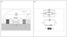
图1为传感器结构设计图。其中,图1(a)为在4英寸晶圆上制造传感器的掩模设计,图1(b)为带有电子测量垫的传感器结构。Figure 1 is a design diagram of the sensor structure. Among them, Figure 1(a) is a mask design for fabricating a sensor on a 4-inch wafer, and Figure 1(b) is a sensor structure with electronic measurement pads.
图2为在洁净室环境中传感器的制造流程中,不同阶段传感器的照片。其中,图2(a)为基板选择和清洁阶段,图2(b)为光刻胶涂层阶段,图2(c)为掩模调整和UV曝光器阶段,图2(d)为光刻步骤和显影阶段,图2(e)为金属沉积和剥离阶段,图2(f)为具有64个叉指电极的IDE传感器示例(电极宽度=8μm,间隙=8μm,长度=1mm)。Figure 2 shows photos of sensors at different stages in the sensor's manufacturing process in a clean room environment. Among them, Figure 2(a) is the substrate selection and cleaning stage, Figure 2(b) is the photoresist coating stage, Figure 2(c) is the mask adjustment and UV exposure stage, and Figure 2(d) is the photolithography stage Steps and development stages, Figure 2(e) is the metal deposition and lift-off stage, Figure 2(f) is an example of an IDE sensor with 64 interdigitated electrodes (electrode width = 8 μm, gap = 8 μm, length = 1 mm).
图3为对已制造的IDE传感器的表面功能化过程示意图。其中,图3(a)为超声清洗,图3(b)为表面活化/羟基(-OH)形成,图3(c)为表面改性中的盐化步骤,图3(d)为表面改性中的聚合物连接附着步骤,图3(e)为表面改性中的将氨基修饰的寡核苷酸探针固定在传感器上的步骤。Figure 3 is a schematic diagram of the surface functionalization process of the fabricated IDE sensor. Among them, Fig. 3(a) is ultrasonic cleaning, Fig. 3(b) is surface activation/hydroxyl (-OH) formation, Fig. 3(c) is the salinization step in surface modification, and Fig. 3(d) is surface modification Figure 3(e) shows the step of immobilizing amino-modified oligonucleotide probes on the sensor in the surface modification.
图4(a)是本发明一个实施例中IDE生物传感器微系统的示意图,图4(b)是本发明一个实施例中阻抗测量电路的等效电路简化图。Fig. 4(a) is a schematic diagram of an IDE biosensor microsystem in an embodiment of the present invention, and Fig. 4(b) is a simplified diagram of an equivalent circuit of an impedance measurement circuit in an embodiment of the present invention.
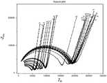
图5是本发明一个实施例中检测HLA-B*15:02(外显子2)时阻抗反应的奈奎斯特示意图。FIG. 5 is a Nyquist schematic diagram of the impedance response when HLA-B*15:02 (exon 2) is detected in an embodiment of the present invention.
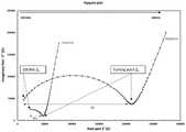
图6是本发明一个实施例中HLA-B*15:02外显子2的LAMP扩增产物每个样本示意图。6 is a schematic diagram of each sample of the LAMP amplification product of HLA-B*15:02 exon 2 in an embodiment of the present invention.
图7是本发明一个实施例中IDE生物传感器表面上结合的HLA-B*15:02的一个阳性与一个阴性LAMP扩增产物的电化学阻抗谱特性。7 is an electrochemical impedance spectroscopy characteristic of one positive and one negative LAMP amplification product of HLA-B*15:02 bound on the surface of the IDE biosensor according to an embodiment of the present invention.
图8是本发明一个实施例中显示基线和杂交后阻抗测量相关ΔZR的表格。Figure 8 is a table showing the ΔZR associated with baseline and post-hybridization impedance measurements in one embodiment of the present invention.
图9是本发明一个实施例基线测量条形图中显示的ΔZR值和清晰显示的目标样本。Figure 9 is the ΔZR value shown in a bar graph of baseline measurements and a clearly displayed target sample for one embodiment of the present invention.
图10是本发明一个实施例中阳性和阴性目标检测测量值之间的统计学t检验结果。Figure 10 is a statistical t-test result between positive and negative target detection measurements in one embodiment of the present invention.
图11是本发明一个实施例中用于阳性和阴性样本检测的生物传感器之间基线测量的统计学t检验结果。Figure 11 is a statistical t-test result of baseline measurements between biosensors for positive and negative sample detection in one embodiment of the present invention.
具体实施方式Detailed ways
为使本发明的目的、技术方案和优点更加清楚,下面将对本发明的技术方案进行详细的描述。显然,所描述的实施例仅仅是本发明一部分实施例,而不是全部的实施例。基于本发明中的实施例,本领域普通技术人员在没有做出创造性劳动的前提下所得到的所有其它实施方式,都属于本发明所保护的范围。In order to make the objectives, technical solutions and advantages of the present invention clearer, the technical solutions of the present invention will be described in detail below. Obviously, the described embodiments are only some, but not all, embodiments of the present invention. Based on the embodiments of the present invention, all other implementations obtained by those of ordinary skill in the art without creative work fall within the protection scope of the present invention.
本发明的目的在于提供一种IDE叉指电极的制作以及预功能化处理方法。上述方法包括在洁净室中使用微纳加工技术制造出间距只有数微米的叉指电极(IDE)结构,并且通过一系列的化学反应成功将和目标基因互补的寡核苷酸探针序列固定在电极上,实现了叉指电极的预功能化。加工后的叉指电极(IDE)可以用于基因序列等遗传学的检测。The purpose of the present invention is to provide a method for fabricating and pre-functionalizing an IDE interdigital electrode. The above method includes using micro-nano processing technology to fabricate an interdigital electrode (IDE) structure with a spacing of only a few microns in a clean room, and successfully immobilizing the oligonucleotide probe sequence complementary to the target gene through a series of chemical reactions. On the electrodes, pre-functionalization of the interdigital electrodes was achieved. The processed interdigital electrode (IDE) can be used for genetic detection such as gene sequence.
为实现上述目的,本发明的技术方案如下:For achieving the above object, technical scheme of the present invention is as follows:
本发明涉及一种IDE叉指电极的制作以及预功能化处理方法,包括以下步骤:The present invention relates to a kind of preparation of IDE interdigital electrode and pre-functionalization treatment method, comprise the following steps:
(1)IDE传感器的制作(1) Production of IDE sensor
(1-1)根据设计的结构制作掩膜版;(1-1) Make a mask according to the designed structure;
掩膜版在IDE传感器的制作中有着最关键的作用,通过它能够将设计好的图案传递到玻璃衬底上并形成对应的电极图案。通过使用电脑辅助设计软件(CAD,KLayot)可以绘制出叉指电极的图案,形成的电子版的二维图可以进行掩膜版的加工。掩膜版的用途是在光刻机(紫外曝光机)的光照下,阻挡部分区域的光线,将掩膜版上的图案转到下层的光刻胶上。根据光刻胶的类型(正性或负性)改变掩膜版的吸光区域。掩膜版常见的制作材料是石英玻璃,金属铬和感光胶,把已设计好的电路图形通过电子激光设备曝光在感光胶上,被曝光的区域会被显影出来,在金属铬上形成电路图形,成为类似曝光后的底片的光掩模版。制造电极传感器前审核设计的相关文件。The mask plays the most critical role in the fabrication of IDE sensors, through which the designed pattern can be transferred to the glass substrate and the corresponding electrode pattern can be formed. By using computer-aided design software (CAD, KLayot), the pattern of the interdigital electrode can be drawn, and the two-dimensional image of the formed electronic version can be used for mask processing. The purpose of the mask is to block the light in part of the area under the light of the photolithography machine (ultraviolet exposure machine), and transfer the pattern on the mask to the photoresist of the lower layer. The light absorbing area of the reticle is changed according to the type of photoresist (positive or negative). The common materials for making masks are quartz glass, metal chrome and photosensitive glue. The designed circuit pattern is exposed on the photosensitive glue through electronic laser equipment, and the exposed area will be developed, and the circuit pattern will be formed on the metal chrome. , which becomes a photomask similar to the exposed negative. The relevant documents for reviewing the design before manufacturing the electrode sensor.
图1显示了包括电极传感器的掩模示例和尺寸。掩模规格如下:电极区域为黑色,阻挡紫外光穿过。使用5英寸的掩膜版制作4英寸的晶片衬底,由墨尔本纳米制造中心(MCN)工艺工程师完成传感器的制造。Figure 1 shows examples and dimensions of masks including electrode sensors. The mask specifications are as follows: the electrode areas are black, blocking the passage of UV light. A 4-inch wafer substrate was fabricated using a 5-inch reticle, and the sensors were fabricated by process engineers at the Melbourne Centre for Nanofabrication (MCN).
(1-2)在洁净室环境中制作IDE生物传感器(1-2) Fabrication of IDE biosensors in a clean room environment
所述IDE生物传感器需要在10000级和100级洁净室环境中制造,保证产品绝对不会受到污染和沉积。不仅操作人员是潜在的污染颗粒载体,室内安装的灯具也需要符合相关参数需求、卫生法规和不同的分类。本发明中涉及到医药行业以及半导体制造业的要求。The IDE biosensor needs to be manufactured in a class 10000 and
本发明提供的IDE传感器是在含有光刻胶涂层的衬底上使用UV光刻技术制造得到。图2展示了具体的制作步骤,首先在玻璃衬底上加上一层光刻胶,这里所用的衬底为4英寸的
由于在晶圆上应用光敏层光刻胶,所以在100级洁净室中,使用琥珀色光进行光刻步骤和图案显影。琥珀色光在半导体制造的光刻工艺中起着重要的作用。由于光刻胶仅在几秒钟内就会显影,因此当使用常见的带有蓝光的白色灯光时,不可能进行可再现的光刻工艺。Since the photosensitive layer photoresist is applied on the wafer, the photolithography steps and pattern development are performed in a
进一步地,上述在洁净室环境中制作IDE生物传感器的具体工艺包括以下步骤:Further, the above-mentioned specific process for making IDE biosensors in a clean room environment includes the following steps:
(1-2-1)在通风橱内对晶圆进行清洗;(1-2-1) Clean the wafer in a fume hood;
优选地,使用丙酮、异丙醇(IPA)、去离子水依次对晶圆进行冲洗,以去除表面的灰尘和有机物,冲洗结束后用氮气(N2)进行干燥清洁,最后用氮气(N2)清除晶圆上的灰尘颗粒。Preferably, acetone, isopropyl alcohol (IPA), and deionized water are used to rinse the wafer in sequence to remove dust and organic matter on the surface. After the rinse, nitrogen (N2 ) is used for drying and cleaning, and finally nitrogen (N2 ) is used for drying and cleaning. ) to remove dust particles from the wafer.
(1-2-2)对所述晶圆进行旋涂;(1-2-2) spin coating the wafer;
优选地,所述晶圆为4英寸晶圆,旋涂采用的设备型号为SUSS Delta 80RC。Preferably, the wafer is a 4-inch wafer, and the type of equipment used for spin coating is SUSS Delta 80RC.
优选地,所述旋涂包括以下步骤:Preferably, the spin coating comprises the following steps:
i.第一次旋涂:在晶圆表面旋涂一层六甲基二硅氨烷(HMDS),增加下一步光刻胶和玻璃衬底的粘附性。旋涂参数为1000-4000rpm持续10-40秒;i. The first spin coating: spin coating a layer of hexamethyldisilazane (HMDS) on the wafer surface to increase the adhesion between the photoresist and the glass substrate in the next step. Spin coating parameters are 1000-4000rpm for 10-40 seconds;
ii.第一次软烘烤:加热光刻胶,蒸发其中的挥发性溶剂。加热温度为100-120℃,持续80-100秒;ii. The first soft bake: the photoresist is heated to evaporate the volatile solvent therein. The heating temperature is 100-120℃ for 80-100 seconds;
iii.第二次旋涂:继续旋涂一层光刻胶,型号为
iv.第二次软烘烤:去除光刻胶中的挥发性溶剂。加热温度为100-120℃,持续80-100秒。iv. Second soft bake: removes volatile solvents from the photoresist. The heating temperature is 100-120°C for 80-100 seconds.
(1-2-3)对所述掩膜版进行光刻掩模对准和紫外线(UV)曝光;(1-2-3) performing photolithography mask alignment and ultraviolet (UV) exposure on the mask;
优选地,所述光刻掩模使用EVG 6200掩模对准器。Preferably, the lithography mask uses an EVG 6200 mask aligner.
优选地,所述光刻掩模的暴露剂量为75mJ/cm2,晶圆和掩模之间为软接触。软接触的含义是通过托盘吸附基片,将掩膜盖在基片上面。这种接触方式较为紧密,光刻分辨率高。Preferably, the exposure dose of the lithography mask is 75 mJ/cm2 , and the wafer and the mask are in soft contact. The meaning of soft contact is to adsorb the substrate through the tray and cover the mask on the substrate. This contact method is relatively tight, and the lithography resolution is high.
光刻掩模的具体过程包括:通过在掩膜对准器中调节掩膜版的位置,使其和玻璃衬底同心。然后打开紫外光对玻璃衬底进行曝光。紫外光先通过掩膜版,掩膜版中透光的部分会有紫外线穿过照射在玻璃衬底的光刻胶上,该部分光刻胶会发生交联固化,在后续的显影中不会被溶解而留下来。没有被紫外光照过的部分在显影中溶解而被去除。The specific process of the photolithography mask includes: adjusting the position of the mask in the mask aligner to make it concentric with the glass substrate. The glass substrate is then exposed to UV light. The ultraviolet light first passes through the mask, and the light-transmitting part of the mask will pass through ultraviolet rays and irradiate on the photoresist of the glass substrate. dissolved and left behind. Parts not exposed to UV light are removed by dissolving during development.
(1-2-4)在通风橱内对所述晶圆进行显影;(1-2-4) developing the wafer in a fume hood;
优选地,所述显影液为

优选地,准备单独的去离子水容器用于冲洗晶圆(通过冲洗停止显影),然后将晶圆浸入显影液中45秒,接着将其直接浸入去离子水中,去除残留在上面的显影液。Preferably, a separate container of deionized water is prepared for rinsing the wafer (development is stopped by rinsing), then the wafer is immersed in the developer solution for 45 seconds, followed by dipping it directly into the deionized water to remove the developer solution remaining on it.
(1-2-5)在偏振光下用显微镜检查显影后的光刻胶图案;(1-2-5) Under polarized light, examine the developed photoresist pattern with a microscope;
优选地,所述检查包括以下步骤:Preferably, the inspection includes the following steps:
i.在偏振光下检查晶圆表面的显影图案是否显影不足或过度显影;i. Check under polarized light whether the developing pattern on the wafer surface is under-developed or over-developed;
ii.如果显影不足,重复步骤(1-2-4);ii. If the development is insufficient, repeat steps (1-2-4);
iii.如果过度显影,停止晶圆上的任何进度步骤,通过去除光刻胶可以重复使用玻璃衬底。剥离光刻胶可通过使用溶剂或碱性介质作为去除剂,即用剥离剂或O2燃烧来实现。iii. If overdeveloped, stop any progress steps on the wafer and the glass substrate can be reused by removing the photoresist. Stripping the photoresist can be achieved by using a solvent or alkaline medium as a remover, i.e. burning with a stripper orO2 .
(1-2-6)采用电子束蒸发器对所述晶圆进行金属沉积,在整个衬底上沉积一层指定厚度的Cr/Au金属;(1-2-6) Use an electron beam evaporator to deposit metal on the wafer, and deposit a layer of Cr/Au metal with a specified thickness on the entire substrate;
优选地,所述电子束蒸发器为Intlvac Nanochrome II。Preferably, the electron beam evaporator is an Intlvac Nanochrome II.
优选地,所述电子束蒸镀包括以下步骤:Preferably, the electron beam evaporation comprises the following steps:
i.在等离子清洗机腔室内进行1分30秒的等离子清洗;i. Plasma cleaning for 1 minute and 30 seconds in the plasma cleaning machine chamber;
ii.进行Cr/Au叠层金属电子束气相沉积:总厚度100nm;ii. Carry out Cr/Au stacked metal electron beam vapor deposition: the total thickness is 100 nm;
这一步中,Cr的最终厚度为10nm,沉积速率为


(1-2-7)在通风柜内对所述晶圆进行金属剥离;(1-2-7) Metal stripping is performed on the wafer in a fume hood;
这一步的作用是:通过去除固化后的光刻胶来去除在光刻胶上方的金属,只留下直接附着在玻璃衬底上的金属,也就是所要的叉指电极部分,包括以下步骤:The function of this step is to remove the metal above the photoresist by removing the cured photoresist, leaving only the metal directly attached to the glass substrate, that is, the desired part of the interdigital electrode, including the following steps:
i.将晶圆放入丙酮中,使用超声波清洁器清洗处理5-10分钟;i. Put the wafer into acetone and use an ultrasonic cleaner for 5-10 minutes;
ii.使用挤压瓶挤出丙酮冲洗晶圆;ii. Use a squeeze bottle to squeeze out acetone to rinse the wafer;
iii.使用新鲜的丙酮溶液重复步骤i)和ii);iii. Repeat steps i) and ii) using fresh acetone solution;
iv.将晶圆浸入异丙醇中,超声处理5分钟;iv. Immerse the wafer in isopropanol and sonicate for 5 minutes;
v.将晶圆浸入去离子水中30秒;v. Immerse the wafer in deionized water for 30 seconds;
vi.取出并用氮气干燥;vi. Take out and dry with nitrogen;
vii.用显微镜和万用表检查特征是否存在短路装置;vii. Use microscope and multimeter to check features for short circuit devices;
viii.如果在晶片上发现残留物,重复步骤i)-vii)或使用光刻胶剥离介质。(1-2-8)对所述晶圆进行高速旋涂,在晶圆表面制备保护层;viii. If residues are found on the wafer, repeat steps i)-vii) or use photoresist to strip the media. (1-2-8) High-speed spin coating is performed on the wafer, and a protective layer is prepared on the surface of the wafer;
优选地,所述高速旋涂采用的设备型号为SUSS Delta 80RC。Preferably, the type of equipment used for the high-speed spin coating is SUSS Delta 80RC.
优选地,所述高速旋涂包括以下步骤:Preferably, the high-speed spin coating comprises the following steps:
i.在晶圆表面旋涂一层光刻胶,型号为
ii.软烘烤去除挥发性溶剂,加热温度为100-120℃,时间为80-100秒。ii. Soft bake to remove volatile solvent, heating temperature is 100-120°C, time is 80-100 seconds.
(1-2-9)对所述晶圆进行湿切割;(1-2-9) Wet cutting the wafer;
优选地,所述湿切割采用的设备型号为Disco DAD321。Preferably, the equipment model used for the wet cutting is Disco DAD321.
优选地,由MCN的工艺工程师进行湿切割后,将切好的玻璃衬底贴在一个塑性膜上,并用环状的塑料环固定在盒子中。此时IDE传感器芯片条已准备好,可以进行下一步,即IDE传感器的表面修饰和探针固定。Preferably, after wet cutting by MCN's process engineers, the cut glass substrate is attached to a plastic film and secured in the box with an annular plastic ring. At this point the IDE sensor chip strip is ready for the next step, which is the surface modification of the IDE sensor and probe immobilization.
(2)IDE传感器的预功能化处理(2) Pre-functionalization of IDE sensor
这一步是在已制造的IDE传感器表面功能化,在有机和无机材料之间建立连接,包括以下步骤:This step is to functionalize the fabricated IDE sensor surface to create a connection between organic and inorganic materials, including the following steps:
(1)IDE传感器的表面清洁;(2)在传感器表面形成羟基(-OH),进行表面活化,(3)通过盐化步骤和聚合物连接进行表面修饰,(4)将带有氨基修饰的寡核苷酸探针连接到传感器固体表面,(5)封闭。上述过程完成后进行生物传感或检测。(1) Surface cleaning of the IDE sensor; (2) Formation of hydroxyl groups (-OH) on the sensor surface for surface activation, (3) Surface modification through a salting step and polymer linkage, (4) Amino-modified Oligonucleotide probes are attached to the sensor solid surface, (5) blocked. After the above process is completed, biosensing or detection is performed.
图3表示对已制造的IDE传感器的表面功能化过程,即在有机和无机材料之间建立键合。其中,图3(a)为超声清洗,图3(b)为表面活化/羟基(-OH)形成,图3(c)为表面改性中的盐化步骤,图3(d)为表面改性中的聚合物连接附着步骤,图3(e)为表面改性中的将氨基修饰的寡核苷酸探针固定在传感器上的步骤。Figure 3 shows the surface functionalization process of the fabricated IDE sensor, i.e. the establishment of bonds between organic and inorganic materials. Among them, Fig. 3(a) is ultrasonic cleaning, Fig. 3(b) is surface activation/hydroxyl (-OH) formation, Fig. 3(c) is the salinization step in surface modification, and Fig. 3(d) is surface modification Figure 3(e) shows the step of immobilizing amino-modified oligonucleotide probes on the sensor in the surface modification.
所述IDE传感器的预功能化处理方法,包括以下步骤:The pre-functionalization processing method of the IDE sensor includes the following steps:
(2-1)采用超声波和溶剂,对所述IDE传感器进行清洗;(2-1) Using ultrasonic waves and solvents to clean the IDE sensor;
申请人需要说明,已制造的传感器在圆形衬底中呈现条状分布,切割方法是湿法切割,传感器上涂有保护性光刻胶层。此外,湿法切割会引入小颗粒污染。因此,生物传感芯片条首先需要进行表面有机清洁。The applicant needs to explain that the fabricated sensor exhibits stripe distribution in a circular substrate, the cutting method is wet cutting, and a protective photoresist layer is coated on the sensor. Additionally, wet cutting introduces small particle contamination. Therefore, the biosensor chip strip first needs to be organically cleaned on the surface.
优选地,所述清洗步骤包括将所述IDE生物传感器分别放入丙酮、异丙醇(IPA)和去离子水中进行超声洗涤,洗涤完成后将所述芯片取出干燥。Preferably, the cleaning step includes putting the IDE biosensor into acetone, isopropyl alcohol (IPA) and deionized water for ultrasonic washing respectively, and taking out the chip for drying after the washing is completed.
在本发明的一个具体实施例中,所述清洗包括以下步骤:In a specific embodiment of the present invention, the cleaning includes the following steps:
i.使用带有密封盖的PET或PP管,进行生物传感芯片的清洁(也可使用玻璃杯或结晶皿);i. Use a PET or PP tube with a sealed lid to clean the biosensor chip (glass cups or crystallization dishes can also be used);
ii.将清洁液注入管中,直至没过待清洁的芯片,盖紧盖子密闭,依次使用丙酮、异丙醇和去离子水进行清洗,每种溶液分别超声5分钟。ii. Inject the cleaning solution into the tube until the chip to be cleaned is not covered, close the lid tightly, wash with acetone, isopropanol and deionized water in sequence, and sonicate each solution for 5 minutes.
iii.洗涤完成后将所述芯片取出,使用氮气喷枪在无油空气或氮气流中进行干燥。iii. After washing, the chip is taken out and dried in oil-free air or nitrogen flow using a nitrogen spray gun.
(2-2)使用等离子清洗机对所述IDE传感器进行表面活化,在其表面形成羟基(-OH);(2-2) Use a plasma cleaner to activate the surface of the IDE sensor to form hydroxyl groups (-OH) on its surface;
等离子系统可用于干法蚀刻、灰化或表面活化工艺,通过低压等离子体工艺去除表面材料,并在玻璃上进行表面活化。活性离子被加速到样品表面,并发生吸附和解吸反应,挥发性反应产物被真空泵排出。等离子清洗系统可同时用于清洁和表面改性。根据材料类型和应用选择活性气体的类型及其比例。当选择气体流速以将等离子体处理室中的真空保持在0.15到0.30托的范围内时,可获得最佳且均匀的处理结果。等离子系统的射频功率可高达400W,这是精心选择的,以避免被蚀刻样品过程中的过度升温。Plasma systems can be used in dry etching, ashing or surface activation processes to remove surface material and surface activation on glass by a low pressure plasma process. Active ions are accelerated to the surface of the sample, and adsorption and desorption reactions occur, and the volatile reaction products are discharged by a vacuum pump. Plasma cleaning systems can be used for both cleaning and surface modification. The type of reactive gas and its proportion are selected according to the material type and application. Optimal and uniform processing results are obtained when the gas flow rate is selected to maintain the vacuum in the plasma processing chamber in the range of 0.15 to 0.30 Torr. The RF power of the plasma system can be as high as 400W, which is carefully chosen to avoid excessive heating of the sample being etched.
等离子清洗机在200W功率(或高功率)、0.30托压力和30sccm空气流量(氧气20.9%、氮气78.1%、氩气0.9%)下进行氧气等离子体处理5分钟,以激活表面,并去除表面功能化后可能导致硅烷生长失败的有机污染物。根据可用性来选择气体类型/混合百分比(例如氧气25%,氩气75%)。Plasma cleaner at 200W power (or high power), 0.30 Torr pressure and 30sccm air flow (oxygen 20.9%, nitrogen 78.1%, argon 0.9%) for 5 minutes with oxygen plasma treatment to activate the surface and remove the surface features Organic contaminants that can cause silane growth failure after chemi- zation. Select gas type/mix percentage based on availability (eg oxygen 25%, argon 75%).
申请人需要说明,如果等离子体系统类型、真空泵类型和气体混合物发生变化,需要更改使用材料和实验程序。如果等离子清洗机已用于其他用途,或一天中首次使用,建议在不将样品放入清洗腔内的情况下运行该系统,这样它将净化清洗机并去除有机物污染。Applicants need to state that if the plasma system type, vacuum pump type, and gas mixture are changed, the materials used and experimental procedures need to be changed. If the plasma cleaner has been used for other purposes, or is being used for the first time of the day, it is recommended to run the system without placing the sample in the cleaning chamber, so it will decontaminate the cleaner and remove organic contamination.
优选地,所述等离子清洗过程中,射频功率为150-300W,优选200W,真空设定值>300.0mtorr(毫托),清洗时间为3-7min,优选5min。Preferably, in the plasma cleaning process, the radio frequency power is 150-300W, preferably 200W, the vacuum setting value is >300.0mtorr (mtorr), and the cleaning time is 3-7min, preferably 5min.
在本发明的一个具体实施例中,所述等离子清洗包括以下步骤:In a specific embodiment of the present invention, the plasma cleaning includes the following steps:
i.打开等离子清洗机,设置所需的射频功率为200W,设置编辑等离子清洗实验过程:设置内部气体压力为0.3托,待荧光开始后打开进气阀,设置进气流速为30sccm。等离子处理时间为5分钟。i. Turn on the plasma cleaning machine, set the required RF power to 200W, and set the editing process of the plasma cleaning experiment: set the internal gas pressure to 0.3 Torr, open the intake valve after the fluorescence starts, and set the intake flow rate to 30sccm. The plasma treatment time was 5 minutes.
ii.将样品装入等离子清洗腔内并关上门。使用镊子夹住样品,传感器区域需要位于上部,倒置会导致划伤/传感器故障。ii. Load the sample into the plasma cleaning chamber and close the door. Use tweezers to hold the sample, the sensor area needs to be on the upper side, inversion will cause scratches/sensor failure.
iii.运行等离子系统运行程序。启动自动循环来运行预先编程的程序;自动启动“大气通风口”对腔室通风,或关闭真空泵并将空气引入腔室,手动启动腔室进行通风。iii. Run the plasma system operating program. Start an automatic cycle to run a pre-programmed program; automatically start the "atmospheric vent" to ventilate the chamber, or turn off the vacuum pump and introduce air into the chamber, and manually start the chamber to ventilate.
iv.当清洗工艺完成且反应腔体处于大气压力下时,将处理过的传感器快速浸入APTES溶液中。iv. When the cleaning process is complete and the reaction chamber is at atmospheric pressure, quickly immerse the treated sensor in the APTES solution.
建议在开始等离子清洗/表面活化步骤之前,先按照下一个步骤(3),即盐碱化步骤准备好APTES溶液。这样传感器在完成表面活化后,可以被快速放入APTES溶液中。It is recommended that the APTES solution be prepared by following the next step (3), the salinization step, before starting the plasma cleaning/surface activation step. In this way, the sensor can be quickly put into the APTES solution after surface activation.
上述表面活化/羟基(-OH)形成过程也可通过食人鱼蚀刻步骤实现,即,将IDE传感器浸入96%H2SO4:30%H2O2(两者体积比为3:1)的溶液中30分钟。The above surface activation/hydroxyl (-OH ) formation process can also be achieved by a piranha etching step, i.e., immersing the IDE sensor in a 96%H2SO4 :30%H2O2 (3 :1 volume ratio) solution for 30 minutes.
(2-3)对所述IDE传感器进行第一次表面改性,即盐化步骤;(2-3) performing the first surface modification on the IDE sensor, that is, the salinization step;
在经过等离子处理之后,玻璃衬底中的二氧化硅能够被激活,从而连接上羟基(-OH)而产生亲水性。此时加入(3-氨基丙基)三乙氧基硅烷(APTES)溶液,硅烷分子会直接和羟基反应,通过硅氧键连接在玻璃衬底上(非金属电极上)。After plasma treatment, the silicon dioxide in the glass substrate can be activated to attach hydroxyl groups (-OH) to make it hydrophilic. At this time, adding (3-aminopropyl)triethoxysilane (APTES) solution, the silane molecule will react with the hydroxyl group directly and connect to the glass substrate (on the non-metallic electrode) through the silicon-oxygen bond.
优选地,采用体积分数为2%的APTES乙醇溶液,对所述IDE传感器进行摇动培养,时间为5min。培养结束后用乙醇对所述IDE传感器进行清洗,即完成盐化。Preferably, the IDE sensor is shaken and cultured with a volume fraction of 2% APTES ethanol solution for 5 minutes. After the incubation, the IDE sensor was washed with ethanol, that is, the salinization was completed.
在本发明的一个具体实施例中,所述盐化包括以下步骤:In a specific embodiment of the present invention, the salinization comprises the following steps:
i.用乙醇制备2%APTES((3-氨基丙基)三乙氧基硅烷)溶液。例如配置20mL的2%APTES溶液需要在19.6mL乙醇中混合0.4mL100%APTES。此步骤需要在等离子清洗前制备好以增加连接的效果。i. Prepare a 2% APTES ((3-aminopropyl)triethoxysilane) solution in ethanol. For example, to prepare 20mL of 2% APTES solution, mix 0.4mL of 100% APTES in 19.6mL of ethanol. This step needs to be prepared before plasma cleaning to increase the effect of the connection.
ii.将预处理(已清洁)的IDE传感器(硼硅玻璃衬底)放入培养皿内。ii. Place the pre-treated (cleaned) IDE sensor (borosilicate glass substrate) in a petri dish.
iii.将APTES溶液倒入培养皿至覆盖传感器,盖上培养皿盖子,并用封口膜密封。iii. Pour the APTES solution into the petri dish to cover the sensor, close the petri dish lid, and seal with parafilm.
iv.使用摇床进行1小时摇动培养。iv. Incubate with shaking for 1 hour using a shaker.
v.从培养皿中倒出APTES溶液,并倒入废液桶中。v. Pour off the APTES solution from the petri dish and into the waste bucket.
vi.用乙醇清洗感应器芯片条,摇床上震动5分钟,重复清洗3次。vi. Wash the sensor chip strip with ethanol, shake on a shaker for 5 minutes, and repeat the washing 3 times.
下一步使用的戊二醛溶液需要在最后一次清洗之前准备好,以减少等待时间并减少风干效果。The glutaraldehyde solution used in the next step needs to be prepared before the final wash to reduce waiting time and reduce air-drying effects.
(2-4)对所述IDE传感器进行第二次表面改性,即连接聚合物;(2-4) The second surface modification is performed on the IDE sensor, that is, the polymer is attached;
APTES的另一端还有氨基,加入戊二醛后,戊二醛能够与氨基结合从而连接在玻璃衬底上。同时戊二醛的另一端有助于连接下一步所需要的DNA探针序列,实现DNA在玻璃衬底上的连接。The other end of APTES also has an amino group. After adding glutaraldehyde, the glutaraldehyde can combine with the amino group to connect to the glass substrate. At the same time, the other end of glutaraldehyde helps to connect the DNA probe sequence required in the next step, so as to realize the connection of DNA on the glass substrate.
优选地,采用体积分数为2.5%的戊二醛水溶液,对所述IDE传感器进行摇动培养,时间为2h。培养结束后用去离子水对所述IDE传感器进行清洗,即完成连接聚合物。Preferably, the IDE sensor is shaken and cultured with a volume fraction of 2.5% glutaraldehyde aqueous solution for 2 hours. After the incubation, the IDE sensor was washed with deionized water, that is, the connection of the polymer was completed.
在本发明的一个具体实施例中,所述连接聚合物包括以下步骤:In a specific embodiment of the present invention, the linking polymer comprises the following steps:
i.制备体积分数为2.5%的戊二醛溶液。20mL的2.5%戊二醛溶液制备如下:在18mL
ii.使用注射器过滤器过滤戊二醛溶液中的杂质。对于25%二级戊二醛溶液,使用0.2μm或0.4μm注射器过滤器去除溶液中的杂质。ii. Use a syringe filter to filter impurities from the glutaraldehyde solution. For 25% secondary glutaraldehyde solution, use a 0.2 μm or 0.4 μm syringe filter to remove impurities from the solution.
iii.将戊二醛溶液倒入培养皿中,没过传感器芯片,盖上培养皿盖子,并用封口膜密封。iii. Pour the glutaraldehyde solution into the petri dish, cover the sensor chip, cover the petri dish, and seal with parafilm.
iv.使用摇床进行2小时摇动培养。iv. Incubate with shaking for 2 hours using a shaker.
v.从培养皿中去除戊二醛溶液,将戊二醛溶液废液倒入废液桶中。v. Remove the glutaraldehyde solution from the petri dish and pour the waste glutaraldehyde solution into the waste bucket.
vi.用
vii.在无油空气或氮气流中干燥传感器芯片条。vii. Dry the sensor chip strip in a stream of oil-free air or nitrogen.
下一步使用的探针溶液需要在最终清洗完成之前准备好,以尽量减少等待及风干影响。The probe solution used in the next step needs to be prepared before the final wash is completed to minimize the effects of waiting and air-drying.
(2-5)对所述IDE传感器进行表面修饰,将氨基修饰的寡核苷酸探针固定在传感器上;(2-5) Surface modification is performed on the IDE sensor, and the amino-modified oligonucleotide probe is immobilized on the sensor;
寡核苷酸探针是根据要检测的目标基因所合成的互补序列。再在探针的5’端进行氨基修饰。氨基能够连接在上述步骤加入的戊二醛,从而实现核苷酸探针在玻璃衬底上的化学连接。本发明所用探针生产厂家为生工生物工程(上海)股份有限公司,为定制DNA序列,无具体型号。Oligonucleotide probes are complementary sequences synthesized according to the target gene to be detected. Amino-modification was performed at the 5' end of the probe. The amino group can be connected to the glutaraldehyde added in the above step, so as to realize the chemical connection of the nucleotide probe on the glass substrate. The manufacturer of the probe used in the present invention is Sangon Bioengineering (Shanghai) Co., Ltd., which is a customized DNA sequence without a specific model.
优选地,将浓度为100μM的末端氨基修饰的生物探针溶液注入IDE传感器表面的IDE传感器条内,在4-5℃培育15-16h,然后进行清洗。Preferably, the terminal amino-modified biological probe solution with a concentration of 100 μM is injected into the IDE sensor strip on the surface of the IDE sensor, incubated at 4-5° C. for 15-16 h, and then washed.
在本发明的一个具体实施例中,所述固定探针包括以下步骤:In a specific embodiment of the present invention, the immobilization probe comprises the following steps:
i.在传感器上贴覆提前准备好的PSA胶带,方便将IDE电极浸入在探针溶液中。以每一传感器芯片条上有6个独立的叉指电极为例,则在PSA胶带上切割6个直径为3-4mm的孔,将胶带贴在玻璃衬底上使得每个IDE传感器位于小孔中央。在培养皿中放入KIMWIPE清洁抹布,并接入
ii.将3.5μL的100μM(或其它需要/优化的摩尔浓度)的末端氨基修饰的生物探针溶液滴到每个孔中。ii. Drop 3.5 μL of 100 μM (or other desired/optimized molar concentration) of the terminal amino-modified biological probe solution into each well.
iii.将带有探针溶液的IDE生物传感芯片放入湿度室内,盖上湿度室盖子后,用封口膜密闭,在4℃冰箱中培育15-16小时。iii. Put the IDE biosensor chip with the probe solution into the humidity chamber, cover with the lid of the humidity chamber, seal with parafilm, and incubate in a 4°C refrigerator for 15-16 hours.
iv.探针培育完成后,用微量移液器去除多余液体后,再用
上述过程中确保载玻片/传感器在洗涤步骤之间以及洗涤和封闭之间不会变干。清洗结束后,应立即进入封闭步骤。下一步实验的封闭液需要在最后一次洗涤之前准备好,最大限度地减少等待并减少风干效应。The above procedure ensures that the slides/sensors do not dry out between washing steps and between washing and blocking. Immediately after cleaning, proceed to the blocking step. The blocking solution for the next experiment needs to be prepared before the final wash, minimizing waiting and reducing air-drying effects.
(2-6)对所述IDE传感器进行封闭(Blocking);(2-6) Blocking the IDE sensor;
封闭培养是使用乙醇胺溶液覆盖在加入了寡核苷酸探针的电极上,保证电极的活性。In the blocking culture, ethanolamine solution is used to cover the electrode with the oligonucleotide probe added to ensure the activity of the electrode.
优选地,将体积分数为1%的乙醇胺水溶液注入IDE传感器表面的IDE传感器条内,对所述IDE传感器进行封闭培养,时间为30min。培养结束后用去离子水对所述IDE传感器进行清洗,即完成封闭过程。Preferably, an aqueous solution of ethanolamine with a volume fraction of 1% is injected into the IDE sensor strip on the surface of the IDE sensor, and the IDE sensor is closed and cultured for 30 minutes. After the incubation, the IDE sensor was washed with deionized water, that is, the sealing process was completed.
在本发明的一个具体实施例中,所述封闭包括以下步骤:In a specific embodiment of the present invention, the sealing includes the following steps:
i.配制体积分数为1%的乙醇胺水溶液作为封闭液。1mL乙醇胺溶液制备如下:将10μL纯度为100%的乙醇胺与990μL
ii.每个孔中滴入10μL1%乙醇胺溶液。ii. Drop 10 μL of 1% ethanolamine solution into each well.
iii.盖上培养皿盖子,并用封口膜密封。iii. Cap the petri dish and seal with parafilm.
iv.培养30分钟。iv. Incubate for 30 minutes.
v.去除封闭液,用
vi.将清洗废液倒入废液桶中。vi. Pour the cleaning waste liquid into the waste liquid bucket.
vii.在无油空气或氮气流中干燥生物传感器芯片条。vii. Dry the biosensor chip strip in a stream of oil-free air or nitrogen.
至此,IDE传感器可以开始进行阻抗测量和目标基因的检测。At this point, the IDE sensor can start to perform impedance measurement and detection of target genes.
对上述封闭后的IED生物传感器进行阻抗测量。阻抗谱是一种强有力的方法,可以用来确定生物传感器系统的响应。目标材料引起的变化可能与溶液的介电常数、物理结构和离子性质的变化有关。由于随后引入的目标,初始系统的这些变化将在阻抗谱中反映为无源电气元件特性变化(电阻、电容和电感)。采用本发明提供的IDE生物传感器进行目标基因检测包括如下步骤:Impedance measurements were performed on the above closed IED biosensors. Impedance spectroscopy is a powerful method that can be used to determine the response of a biosensor system. The changes induced by the target material may be related to changes in the dielectric constant, physical structure, and ionic properties of the solution. These changes to the initial system will be reflected in the impedance spectrum as changes in passive electrical component properties (resistance, capacitance, and inductance) due to subsequently introduced targets. Using the IDE biosensor provided by the present invention to detect the target gene comprises the following steps:
步骤S101、在IDE生物传感器上固定检测待测样本的目标基因探针(前述部分已完成);Step S101, fixing the target gene probe for detecting the sample to be tested on the IDE biosensor (the previous part has been completed);
步骤S102、所述待测样本与所述目标基因探针结合后发生反应,得到电信号数据的实部和虚部;所述电信号数据为电路的阻抗数据。Step S102, the sample to be tested is combined with the target gene probe and reacts to obtain the real part and the imaginary part of the electrical signal data; the electrical signal data is the impedance data of the circuit.
阻抗谱是一种强有力的方法,可以用来确定生物传感器系统的响应。目标材料引起的变化可能与溶液的介电常数、物理结构和离子性质的变化有关。由于随后引入的目标,初始系统的这些变化将在阻抗谱中反映为无源电气元件特性变化(电阻、电容和电感)。请参阅图4(a),图4(a)是IDE生物传感器微系统的示意图,用于检测电极之间的DNA杂交孵育,并指示所有无源电路组件。每个组成部分解释如下。Impedance spectroscopy is a powerful method that can be used to determine the response of a biosensor system. The changes induced by the target material may be related to changes in the dielectric constant, physical structure, and ionic properties of the solution. These changes to the initial system will be reflected in the impedance spectrum as changes in passive electrical component properties (resistance, capacitance, and inductance) due to subsequently introduced targets. Please refer to Figure 4(a), which is a schematic diagram of the IDE biosensor microsystem for the detection of DNA hybridization incubation between electrodes and indicates all passive circuit components. Each component is explained below.
(1)Rct–金属间电荷转移电阻-测量溶液;(1) Rct - Intermetallic charge transfer resistance - measuring solution;
(2)Rsol–测量溶液的电阻;(2) Rsol – measure the resistance of the solution;
(3)Rbio–电极之间固定的DNA分子、有机物和聚合物(生物识别元件层)的电阻;(3) Rbio – the resistance of DNA molecules, organics and polymers (layers of biological recognition elements) immobilized between electrodes;
(4)Csol–测量溶液的寄生电容;(4) Csol – measure the parasitic capacitance of the solution;
(5)Csub–玻璃基板的寄生电容;(5) Csub – the parasitic capacitance of the glass substrate;
(6)Cdl–金属间的双层电容-测量溶液。(6)Cdl - Intermetallic Double Layer Capacitance - Measurement Solution.
请参阅图4(b),图4(b)是阻抗测量电路的等效电路简化图,即上述相应的电气元件可简化为一个等效电路模型。如下所示:Please refer to FIG. 4(b), FIG. 4(b) is a simplified equivalent circuit diagram of the impedance measurement circuit, that is, the above-mentioned corresponding electrical components can be simplified into an equivalent circuit model. As follows:
(1)Csol和Csub视为与Ccell=Csol+Csub.等效的并联电容器;(1) Csol and Csub are regarded as parallel capacitors equivalent to Ccell =Csol +Csub .
(2)Rsol和Rbio被认为是与Rcell=((Rsol)-1+(Rbio)-1)-1等价的并联电容器;(2) Rsol and Rbio are considered as parallel capacitors equivalent to Rcell =((Rsol )-1 +(Rbio )-1 )-1 ;
(3)在实践中,以Warburg阻抗ZW.来代表Rct(金属-测量溶液之间的电荷转移电阻)和Cdl(金属-测量溶液之间的双层电容)在低频下的效应。(3) In practice, the Warburg impedance ZW. is used to represent the effect of Rct (the charge transfer resistance between the metal-measuring solutions) and Cdl (the double-layer capacitance between the metal-measuring solutions) at low frequencies.
它可以被认为是一个具有相当于Zcell=Zreal-jZimaginary(笛卡尔形式)值的复阻抗的电化学电池,其中阻抗的实部是Zreal,虚部是Zimaginary。阻抗的幅值和相位可通过以下关系式得出:It can be thought of as an electrochemical cell with a complex impedance equivalent to a value of Zcell = Zreal - jZimaginary (in Cartesian form), where the real part of the impedance is Zreal and the imaginary part is Zimaginary . The magnitude and phase of the impedance are given by the following relationship:
(1)幅值阻抗,|Zcell|=(ZcellZ*cell)1/2=(Z2real+Z2imaginary)1/2;(1) Amplitude impedance, |Zcell |=(Zcell Z*cell )1/2 =(Z2real +Z2imaginary )1/2 ;
(2)阻抗相位,-θ=tan-1(-Zimaginary/Zreal)。(2) Impedance phase, -θ=tan-1 (-Zimaginary /Zreal ).
在典型的电化学阻抗测量中,利用频率响应分析仪(FRA)模块根据所述电信号数据按预设频率和振幅生成正弦波。该信号叠加在电池上施加的直流电位或电流上。通过两个频率响应分析仪通道分析交流电压和电流分量,计算传递函数、总阻抗、相位角偏移以及总阻抗的实部和虚部。In a typical electrochemical impedance measurement, a frequency response analyzer (FRA) module is used to generate a sine wave at a preset frequency and amplitude from the electrical signal data. This signal is superimposed on the DC potential or current applied to the battery. The AC voltage and current components are analyzed through two frequency response analyzer channels to calculate the transfer function, total impedance, phase angle shift, and the real and imaginary parts of the total impedance.
需要说明的是,计算传递函数、总阻抗、相位角偏移以及总阻抗的实部和虚部是频率响应分析仪自带的功能。It should be noted that calculating the transfer function, total impedance, phase angle offset, and the real and imaginary parts of the total impedance are functions that come with the frequency response analyzer.
步骤S103、根据所述电信号数据的实部和虚部判断所述待测样本是否含有所述目标基因。Step S103: Determine whether the sample to be tested contains the target gene according to the real part and the imaginary part of the electrical signal data.
在一个实施例中,当要检测的目标基因和连接在玻璃衬底的探针结合后,电路的阻抗特性会发生改变,例如从EIS阻抗谱中可以看到高频率段(半圆形部分)实部电阻值将会减小。而检测的样本中如果没有目标DNA,则在清洗后没有DNA能够与之前连接的探针相结合,测量得到实部阻抗值偏大。因此在测量的样本与修饰过的IDE电极杂交后再进行阻抗测量能够知道样本的阴阳性。In one embodiment, when the target gene to be detected is combined with the probe connected to the glass substrate, the impedance characteristics of the circuit will change, for example, a high frequency band (semi-circular part) can be seen from the EIS impedance spectrum. The real part resistance value will decrease. However, if there is no target DNA in the detected sample, no DNA can be combined with the previously connected probe after washing, and the measured impedance value of the real part is too large. Therefore, after the measured sample is hybridized with the modified IDE electrode, the impedance measurement can be performed to know whether the sample is negative or positive.
作为上述方法的进一步改进,在一个实施例中,所述根据所所述电信号数据的实部和虚部判断所述待测样本是否含有目标基因,包括:As a further improvement of the above method, in one embodiment, determining whether the sample to be tested contains the target gene according to the real part and the imaginary part of the electrical signal data includes:
计算所述转折点处的实部阻抗值与预设阈值的差值,若所述转折点处的实部阻抗值大于预设阈值,则所述待测样本中不含有目标基因。Calculate the difference between the real impedance value at the turning point and a preset threshold, and if the real impedance value at the turning point is greater than the preset threshold, the sample to be tested does not contain the target gene.
作为上述方法的进一步改进,在一个实施例中,所述根据所所述电信号数据的实部和虚部判断所述待测样本是否含有目标基因,包括:As a further improvement of the above method, in one embodiment, determining whether the sample to be tested contains the target gene according to the real part and the imaginary part of the electrical signal data includes:
计算所述转折点处的实部阻抗值与预设阈值的差值,若所述转折点处的实部阻抗值小于预设阈值,则所述待测样本中含有目标基因。Calculate the difference between the real impedance value at the turning point and a preset threshold, and if the real impedance value at the turning point is less than the preset threshold, the sample to be tested contains the target gene.
请参阅图5,图5是本发明一个实施例中检测HLA-B*15:02(外显子2)时阻抗反应的奈奎斯特示意图,如图5所示,图中显示了来自HLA-B*15:02外显子2的阳性LAMP扩增产物、外显子2的阴性LAMP扩增产物、无DNA模板对照组NTC,以及所有样本的基线测量结果。Please refer to FIG. 5. FIG. 5 is a Nyquist schematic diagram of the impedance response when HLA-B*15:02 (exon 2) is detected in an embodiment of the present invention, as shown in FIG. -B*15:02 Positive LAMP amplification product of exon 2, negative LAMP amplification product of exon 2, no DNA template control NTC, and baseline measurements of all samples.
请参阅图6,图6是本发明一个实施例中HLA-B*15:02外显子2的LAMP扩增产物每个样本示意图。Please refer to FIG. 6. FIG. 6 is a schematic diagram of each sample of the LAMP amplification product of HLA-B*15:02 exon 2 in an embodiment of the present invention.
请参阅图7,图7是本发明一个实施例中IDE生物传感器表面上结合的HLA-B*15:02的LAMP扩增产物的电化学阻抗谱特性。Please refer to FIG. 7 , which is an electrochemical impedance spectroscopy characteristic of the LAMP amplification product of HLA-B*15:02 bound on the surface of the IDE biosensor according to an embodiment of the present invention.
本发明使用了两个传感器阻抗响应的奈奎斯特表示法和ΔZR=Zreal(转折点)-Zreal(100kHz)的计算方法。The present invention uses the Nyquist representation of the impedance response of the two sensors and the calculation method of ΔZR = Zreal (turning point) - Zreal (100 kHz).
如图5-7的阻抗曲线所示,奈奎斯特图的横坐标为整个系统的实部阻值,纵坐标表示整个系统的虚部阻值。可以看到阻抗的曲线图为一个弧形加一段直线部分,弧形为高频时的曲线,直线为低频时的曲线。转折处的实部阻抗是电阻的阻值加上电容的阻抗。在LAMP阳性产物结合在电极上之后就会改变电容的阻抗导致圆弧变小,也就是实部的阻抗很小。而LAMP阴性产物不会结合在电极上,对电容阻抗的改变不大。As shown in the impedance curve in Figure 5-7, the abscissa of the Nyquist diagram represents the real resistance of the entire system, and the ordinate represents the imaginary resistance of the entire system. It can be seen that the curve of impedance is an arc plus a straight line, the arc is the curve at high frequencies, and the straight line is the curve at low frequencies. The real impedance at the break is the resistance of the resistor plus the impedance of the capacitor. After the LAMP positive product is bound to the electrode, it will change the impedance of the capacitor and cause the arc to become smaller, that is, the impedance of the real part is very small. The LAMP-negative product does not bind to the electrode and does not change the capacitive impedance much.
因此,可以通过测量ΔZR来判断样本的阴阳性。根据绝对值可以认为ZR小于预设临界值就是阳性,或者根据统计学方法判断ZR是否在阳性范围内。Therefore, the negative or positive of the sample can be judged by measuring ΔZR. According to the absolute value, it can be considered that the ZR is less than the preset critical value as positive, or whether the ZR is within the positive range can be judged according to statistical methods.
作为上述方法的进一步改进,在一个实施例中,所述根据所所述电信号数据的实部和虚部判断所述待测样本是否含有目标基因,包括:As a further improvement of the above method, in one embodiment, determining whether the sample to be tested contains the target gene according to the real part and the imaginary part of the electrical signal data includes:
若所述实部阻抗值不大于预设阻抗值,则所述待测样本中含有目标基因。If the real impedance value is not greater than the preset impedance value, the sample to be tested contains the target gene.
一些实施例中,所述电信号数据包括所述待测样本与所述目标基因探针结合时电极或电极间隙表面形成复合物的介电性质、电荷分布、表面物理性质、尺寸和形状的变化。In some embodiments, the electrical signal data includes changes in the dielectric properties, charge distribution, surface physical properties, size and shape of the complex formed on the electrode or electrode gap surface when the test sample is combined with the target gene probe. .
本申请对每个目标检测的阻抗测量数据进行分析/比较,如图5所示,图中包括:The present application analyzes/compares the impedance measurement data detected by each target, as shown in Figure 5, which includes:
基线,基线是指传感器在没加样本之前进行测量,得到的曲线,基线是带正方形标记的线;Baseline, the baseline refers to the curve obtained by measuring the sensor before adding the sample, and the baseline is the line with a square mark;
已知样本为阴性经过检测后得到的曲线是用带三角形标记的线,其中掺杂了2个带五角星的线是blank空白对照,也可以算阴性。The curve obtained after the sample is known to be negative is the line marked with a triangle, and the line with two five-pointed stars is a blank control, which can also be regarded as negative.
已知样本为阳性是经过检测后得到的曲线是用圆圈标记的线。Known samples that are positive are tested and the resulting curve is the line marked with a circle.
由此得出统计学结果,对于未知样本进行检测时候,若未知样本转折点处的实部阻抗值小于预设阈值,则所述待测样本中含有目标基因。From this, a statistical result is obtained. When the unknown sample is detected, if the real impedance value at the turning point of the unknown sample is less than the preset threshold, the sample to be tested contains the target gene.
若未知样本转折点处的实部阻抗值大于预设阈值,则所述待测样本中不含有目标基因。If the real impedance value at the turning point of the unknown sample is greater than the preset threshold, the sample to be tested does not contain the target gene.
其中,预设的阈值可以根据实际测量中的统计结果得出。Wherein, the preset threshold value can be obtained according to the statistical result in the actual measurement.
用于检测HLA-B*15:02(外显子2)的阻抗反应的奈奎斯特图表示清楚地显示了HLA-B*15:02外显子2的LAMP阳性扩增产物和LAMP阴性扩增产物之间的差异,这证明了这项新技术的工作原理。The Nyquist plot representation used to detect the impedance response of HLA-B*15:02 (exon 2) clearly shows the LAMP-positive and LAMP-negative amplification products of HLA-B*15:02 exon 2 differences between amplification products, which demonstrate how the new technique works.
接下来,对奈奎斯特图中清晰显示的一个特征进行统计分析,以便更好地进行分类。在这方面,如图6所示,在图5的基础上增加了具体的样本的标签,N1到N12号代表阴性样本。P1到P8号代表阳性样本。B1到B2号代表空白对照样本。Next, perform statistical analysis on one feature clearly shown in the Nyquist plot for better classification. In this regard, as shown in Figure 6, the labels of specific samples are added on the basis of Figure 5, and numbers N1 to N12 represent negative samples. Numbers P1 to P8 represent positive samples. Numbers B1 to B2 represent blank control samples.
本发明计算了所用每个传感器在虚部最小(转折点)时阻抗实部与100kHz频率下阻抗实部之间的差异。如图7所示,理论上,这种差异将代表电极之间固定的DNA分子、有机物和聚合物(生物识别元件层)的电阻变化(RDNA)。The present invention calculates the difference between the real part of the impedance at which the imaginary part is minimum (the turning point) and the real part of the impedance at a frequency of 100 kHz for each sensor used. As shown in Figure 7, in theory, this difference would represent the resistance change (RDNA) of the immobilized DNA molecules, organics, and polymers (layers of biorecognition elements) between the electrodes.
ΔZR=Zreal(转折点)-Zreal(100kHz)ΔZR = Zreal (turning point) - Zreal (100kHz)
请参阅图8,图8是本发明一个实施例提供的显示基线和杂交后阻抗测量相关ΔZR的表格。在LAMP实验中进行了外显子2的等温扩增,产物与生物传感器结合后,测量目标相关的ΔZR。Please refer to FIG. 8, which is a table showing the correlation ΔZR of the baseline and post-hybridization impedance measurements provided by one embodiment of the present invention. Isothermal amplification of exon 2 was performed in the LAMP experiment, and after the product was bound to the biosensor, the target-relatedΔZR was measured.
请参阅图9,图9是基线测量条形图中显示的ΔZR值和清晰显示的目标样本。阳性和阴性之间的统计学t检验结果表现了明显的统计显著性差异(p<0.0001)。Please refer to Figure 9 for the ΔZR value displayed in the bar graph of the baseline measurement and the target sample clearly displayed. Statistical t-test results between positive and negative showed a statistically significant difference (p<0.0001).
图8和图9显示了所用每个传感器(基线和目标杂交后)的ΔZR。通过在进行正态性检验后进行统计t检验,使用GraphPad Prism8.0软件进行数据分析,评估传感器的基线测量和每个目标杂交后传感器的性能。p值≤0.05被认为具有统计学意义。Figures 8 and 9 show the ΔZR for each sensor used (baseline and after target hybridization). The baseline measurements of the sensors and the performance of the sensors after hybridization for each target were assessed by performing statistical t-tests followed by normality tests and data analysis using GraphPad Prism 8.0 software. A p-value ≤ 0.05 was considered statistically significant.
请参阅图10,图10是本发明一个实施例中阳性和阴性目标检测测量值之间的统计学t检验结果。Please refer to FIG. 10, which is a statistical t-test result between positive and negative target detection measurements in one embodiment of the present invention.
请参阅图11,图11是本发明一个实施例中用于阳性和阴性样本检测的生物传感器之间基线测量的统计学t检验结果。Please refer to FIG. 11, which is a statistical t-test result of baseline measurements between biosensors for positive and negative sample detection in one embodiment of the present invention.
如图10和图11所示,在阳性和阴性扩增样本杂交传感器后读数组之间进行的t检验显示出明显的统计显著性差异(p<0.0001),这证明了生物传感器作应用时未受到影响。As shown in Figures 10 and 11, a t-test performed between the read sets after hybridization of the sensor with positive and negative amplified samples showed a statistically significant difference (p<0.0001), demonstrating that the biosensor did not function well when applied. affected.
以上所述,仅为本发明的具体实施方式,但本发明的保护范围并不局限于此,任何熟悉本技术领域的技术人员在本发明揭露的技术范围内,可轻易想到变化或替换,都应涵盖在本发明的保护范围之内。因此,本发明的保护范围应以所述权利要求的保护范围为准。The above are only specific embodiments of the present invention, but the protection scope of the present invention is not limited to this. Any person skilled in the art can easily think of changes or substitutions within the technical scope disclosed by the present invention. should be included within the protection scope of the present invention. Therefore, the protection scope of the present invention should be based on the protection scope of the claims.
Claims (10)
Translated fromChinesePriority Applications (1)
| Application Number | Priority Date | Filing Date | Title |
|---|---|---|---|
| CN202210384405.4ACN114858889A (en) | 2022-04-13 | 2022-04-13 | Fabrication of IDE Interdigital Electrode and Pre-functionalization Treatment Method |
Applications Claiming Priority (1)
| Application Number | Priority Date | Filing Date | Title |
|---|---|---|---|
| CN202210384405.4ACN114858889A (en) | 2022-04-13 | 2022-04-13 | Fabrication of IDE Interdigital Electrode and Pre-functionalization Treatment Method |
Publications (1)
| Publication Number | Publication Date |
|---|---|
| CN114858889Atrue CN114858889A (en) | 2022-08-05 |
Family
ID=82632057
Family Applications (1)
| Application Number | Title | Priority Date | Filing Date |
|---|---|---|---|
| CN202210384405.4APendingCN114858889A (en) | 2022-04-13 | 2022-04-13 | Fabrication of IDE Interdigital Electrode and Pre-functionalization Treatment Method |
Country Status (1)
| Country | Link |
|---|---|
| CN (1) | CN114858889A (en) |
Cited By (1)
| Publication number | Priority date | Publication date | Assignee | Title |
|---|---|---|---|---|
| CN115287169A (en)* | 2022-09-30 | 2022-11-04 | 常州先趋医疗科技有限公司 | Detection device based on finger insertion electrode and working method and machining method thereof |
Citations (6)
| Publication number | Priority date | Publication date | Assignee | Title |
|---|---|---|---|---|
| EP1003033A1 (en)* | 1998-11-17 | 2000-05-24 | Interuniversitair Micro-Elektronica Centrum Vzw | Sensor comprising an oligomer binding layer and method of making such sensor and arrays of such sensors |
| US20090084686A1 (en)* | 2006-07-13 | 2009-04-02 | Wan-Soo Yun | Biosensor comprising interdigitated electrode sensor units |
| US20140018262A1 (en)* | 2011-02-28 | 2014-01-16 | Lexogen Gmbh | Biosensor array formed by junctions of functionalized electrodes |
| CN108026571A (en)* | 2015-07-08 | 2018-05-11 | 爱丁堡大学董事会 | Biology sensor |
| US20190187090A1 (en)* | 2016-05-13 | 2019-06-20 | Fraunhofer-Gesellschaft Zur Foerderung Der Angewandten Forschung E.V. | Biosensor, Process for its Preparation and Method for Detecting an Analyte Using the Biosensor |
| CN111965231A (en)* | 2020-07-31 | 2020-11-20 | 华中科技大学 | Semiconductor sensor for virus detection and preparation method and application thereof |
- 2022
- 2022-04-13CNCN202210384405.4Apatent/CN114858889A/enactivePending
Patent Citations (6)
| Publication number | Priority date | Publication date | Assignee | Title |
|---|---|---|---|---|
| EP1003033A1 (en)* | 1998-11-17 | 2000-05-24 | Interuniversitair Micro-Elektronica Centrum Vzw | Sensor comprising an oligomer binding layer and method of making such sensor and arrays of such sensors |
| US20090084686A1 (en)* | 2006-07-13 | 2009-04-02 | Wan-Soo Yun | Biosensor comprising interdigitated electrode sensor units |
| US20140018262A1 (en)* | 2011-02-28 | 2014-01-16 | Lexogen Gmbh | Biosensor array formed by junctions of functionalized electrodes |
| CN108026571A (en)* | 2015-07-08 | 2018-05-11 | 爱丁堡大学董事会 | Biology sensor |
| US20190187090A1 (en)* | 2016-05-13 | 2019-06-20 | Fraunhofer-Gesellschaft Zur Foerderung Der Angewandten Forschung E.V. | Biosensor, Process for its Preparation and Method for Detecting an Analyte Using the Biosensor |
| CN111965231A (en)* | 2020-07-31 | 2020-11-20 | 华中科技大学 | Semiconductor sensor for virus detection and preparation method and application thereof |
Non-Patent Citations (3)
| Title |
|---|
| WANG, LEI等: "A sensitive DNA capacitive biosensor using interdigitated electrodes", BIOSENSORS & BIOELECTRONICS, vol. 87, pages 646 - 653* |
| 颜小飞;汪懋华;安冬;: "基于叉指阵列微电极的阻抗免疫传感器研究进展", 分析化学, no. 10, pages 148 - 157* |
| 黎颖茵;孙浩;左兆瑞;毛红菊;钱大宏;: "定量分析癌胚抗原的谐振式无线生物传感器", 传感器与微系统, no. 06, pages 64 - 66* |
Cited By (1)
| Publication number | Priority date | Publication date | Assignee | Title |
|---|---|---|---|---|
| CN115287169A (en)* | 2022-09-30 | 2022-11-04 | 常州先趋医疗科技有限公司 | Detection device based on finger insertion electrode and working method and machining method thereof |
Similar Documents
| Publication | Publication Date | Title |
|---|---|---|
| CN103913486B (en) | The preparation method of AuNPs-PDMS compound mems thin film biosensor | |
| CN113960128B (en) | Silicon nanowire field effect transistor biosensor based on modification of potassium ion aptamer | |
| CN103713022B (en) | Preparation method of polydimethylsiloxane microfilm capacitive biosensor | |
| CN101592627A (en) | Integrated method for fabricating multi-channel high-sensitivity biosensors | |
| KR102101941B1 (en) | Manufacturing method of biosensor device | |
| Castiello et al. | Interfacial capacitance immunosensing using interdigitated electrodes: the effect of insulation/immobilization chemistry | |
| CN106546727B (en) | A kind of preparation method of Graphene glass chip | |
| CN101271114A (en) | Enzyme-catalyzed conductometric immunosensor based on micro-gap array electrode and its immunodetection method | |
| Bhalla et al. | Dual-mode refractive index and charge sensing to investigate complex surface chemistry on nanostructures | |
| Muaz et al. | Fabrication of interdigitated electrodes (IDE's) by conventional photolithography technique for pH measurement using micro-gap structure | |
| CN114858889A (en) | Fabrication of IDE Interdigital Electrode and Pre-functionalization Treatment Method | |
| CN110006975A (en) | A kind of biosensor based on AFP and preparation method thereof | |
| Hou et al. | Ultrasensitive Detection of SARS‐CoV‑2 by Flexible Metal Oxide Field‐Effect Transistors | |
| CN110865113A (en) | A method for modifying the interface of field-effect transistor sensors based on DNA nanomachines | |
| CN103966321A (en) | Preparation method for regioselective biological-contamination resistant array chip | |
| KR101608817B1 (en) | Electrode structure for capacitive biosensor having interdigitated electrode, method for manufacturing the electrode structure, and capacitive biosensor having the electrode structure | |
| CN115389586B (en) | A graphene biosensor and preparation method thereof | |
| TWI470224B (en) | Detecting system and detecting method | |
| CN111194406A (en) | Carbon nanotube-based device for sensing molecular interactions | |
| TWI454693B (en) | Integrated bio-sensing chip system | |
| Gheorghiu et al. | Electrochemical behavior of oxazoline‐based plasma polymers for biosensing applications | |
| Pires Carneiro | Development of an Electrochemical Biosensor Platform and a Suitable Low-Impedance Surface Modification Strategy | |
| US20070152351A9 (en) | Topographically indexed support substrates | |
| CN117949517A (en) | Graphene transistor chip for simultaneously and rapidly detecting multiple biomarkers in specificity | |
| CN120507421A (en) | Measuring method of biosensor based on two-dimensional miniature field effect transistor electrode |
Legal Events
| Date | Code | Title | Description |
|---|---|---|---|
| PB01 | Publication | ||
| PB01 | Publication | ||
| SE01 | Entry into force of request for substantive examination | ||
| SE01 | Entry into force of request for substantive examination | ||
| RJ01 | Rejection of invention patent application after publication | ||
| RJ01 | Rejection of invention patent application after publication | Application publication date:20220805 |