CN114852947A - MEMS electrode device for cardiac pulse field ablation and preparation method thereof - Google Patents
MEMS electrode device for cardiac pulse field ablation and preparation method thereofDownload PDFInfo
- Publication number
- CN114852947A CN114852947ACN202210422714.6ACN202210422714ACN114852947ACN 114852947 ACN114852947 ACN 114852947ACN 202210422714 ACN202210422714 ACN 202210422714ACN 114852947 ACN114852947 ACN 114852947A
- Authority
- CN
- China
- Prior art keywords
- layer
- electrode
- insulating layer
- temperature
- ablation
- Prior art date
- Legal status (The legal status is an assumption and is not a legal conclusion. Google has not performed a legal analysis and makes no representation as to the accuracy of the status listed.)
- Granted
Links
Images


Classifications
- B—PERFORMING OPERATIONS; TRANSPORTING
- B81—MICROSTRUCTURAL TECHNOLOGY
- B81B—MICROSTRUCTURAL DEVICES OR SYSTEMS, e.g. MICROMECHANICAL DEVICES
- B81B7/00—Microstructural systems; Auxiliary parts of microstructural devices or systems
- B81B7/02—Microstructural systems; Auxiliary parts of microstructural devices or systems containing distinct electrical or optical devices of particular relevance for their function, e.g. microelectro-mechanical systems [MEMS]
- A—HUMAN NECESSITIES
- A61—MEDICAL OR VETERINARY SCIENCE; HYGIENE
- A61B—DIAGNOSIS; SURGERY; IDENTIFICATION
- A61B18/00—Surgical instruments, devices or methods for transferring non-mechanical forms of energy to or from the body
- B—PERFORMING OPERATIONS; TRANSPORTING
- B81—MICROSTRUCTURAL TECHNOLOGY
- B81C—PROCESSES OR APPARATUS SPECIALLY ADAPTED FOR THE MANUFACTURE OR TREATMENT OF MICROSTRUCTURAL DEVICES OR SYSTEMS
- B81C1/00—Manufacture or treatment of devices or systems in or on a substrate
- B81C1/00015—Manufacture or treatment of devices or systems in or on a substrate for manufacturing microsystems
- B81C1/00134—Manufacture or treatment of devices or systems in or on a substrate for manufacturing microsystems comprising flexible or deformable structures
- B81C1/00166—Electrodes
- A—HUMAN NECESSITIES
- A61—MEDICAL OR VETERINARY SCIENCE; HYGIENE
- A61B—DIAGNOSIS; SURGERY; IDENTIFICATION
- A61B18/00—Surgical instruments, devices or methods for transferring non-mechanical forms of energy to or from the body
- A61B2018/00315—Surgical instruments, devices or methods for transferring non-mechanical forms of energy to or from the body for treatment of particular body parts
- A61B2018/00345—Vascular system
- A61B2018/00351—Heart
- A61B2018/00375—Ostium, e.g. ostium of pulmonary vein or artery
- A—HUMAN NECESSITIES
- A61—MEDICAL OR VETERINARY SCIENCE; HYGIENE
- A61B—DIAGNOSIS; SURGERY; IDENTIFICATION
- A61B18/00—Surgical instruments, devices or methods for transferring non-mechanical forms of energy to or from the body
- A61B2018/00571—Surgical instruments, devices or methods for transferring non-mechanical forms of energy to or from the body for achieving a particular surgical effect
- A61B2018/00613—Irreversible electroporation
- A—HUMAN NECESSITIES
- A61—MEDICAL OR VETERINARY SCIENCE; HYGIENE
- A61B—DIAGNOSIS; SURGERY; IDENTIFICATION
- A61B18/00—Surgical instruments, devices or methods for transferring non-mechanical forms of energy to or from the body
- A61B2018/00636—Sensing and controlling the application of energy
- A61B2018/00773—Sensed parameters
- A61B2018/00791—Temperature
- A—HUMAN NECESSITIES
- A61—MEDICAL OR VETERINARY SCIENCE; HYGIENE
- A61B—DIAGNOSIS; SURGERY; IDENTIFICATION
- A61B18/00—Surgical instruments, devices or methods for transferring non-mechanical forms of energy to or from the body
- A61B2018/00636—Sensing and controlling the application of energy
- A61B2018/00773—Sensed parameters
- A61B2018/00839—Bioelectrical parameters, e.g. ECG, EEG
- A—HUMAN NECESSITIES
- A61—MEDICAL OR VETERINARY SCIENCE; HYGIENE
- A61B—DIAGNOSIS; SURGERY; IDENTIFICATION
- A61B18/00—Surgical instruments, devices or methods for transferring non-mechanical forms of energy to or from the body
- A61B2018/00636—Sensing and controlling the application of energy
- A61B2018/00773—Sensed parameters
- A61B2018/00875—Resistance or impedance
- B—PERFORMING OPERATIONS; TRANSPORTING
- B81—MICROSTRUCTURAL TECHNOLOGY
- B81B—MICROSTRUCTURAL DEVICES OR SYSTEMS, e.g. MICROMECHANICAL DEVICES
- B81B2201/00—Specific applications of microelectromechanical systems
- B81B2201/06—Bio-MEMS
Landscapes
- Engineering & Computer Science (AREA)
- Manufacturing & Machinery (AREA)
- Health & Medical Sciences (AREA)
- Microelectronics & Electronic Packaging (AREA)
- Surgery (AREA)
- Life Sciences & Earth Sciences (AREA)
- Medical Informatics (AREA)
- Heart & Thoracic Surgery (AREA)
- Biomedical Technology (AREA)
- Molecular Biology (AREA)
- Animal Behavior & Ethology (AREA)
- General Health & Medical Sciences (AREA)
- Public Health (AREA)
- Veterinary Medicine (AREA)
- Otolaryngology (AREA)
- Nuclear Medicine, Radiotherapy & Molecular Imaging (AREA)
- Computer Hardware Design (AREA)
- Measurement And Recording Of Electrical Phenomena And Electrical Characteristics Of The Living Body (AREA)
Abstract
Translated fromChinese
Description
Translated fromChinese技术领域technical field
本发明涉及电生理器械技术领域,具体地,涉及一种用于心脏脉冲场消融的MEMS电极器件及其制备方法。The invention relates to the technical field of electrophysiological instruments, in particular, to a MEMS electrode device for cardiac pulse field ablation and a preparation method thereof.
背景技术Background technique
心房颤动是临床中最常见的持续性心律失常,它具有较高的发病率和死亡率,并且发病风险随着年龄的增长而增加,影响了1-2%的人群。大约90%的心房颤动是由于异常电信号经由肺静脉进入心房,从而导致不规则的心电图信号。迄今为止,利用导管消融技术进行肺静脉隔离是介入性手术治疗心房颤动的基石。与药物治疗相比,导管消融术因其安全性高、效率高、效果好而成为首选治疗方法。Atrial fibrillation is the most common sustained arrhythmia in clinical practice, it has high morbidity and mortality, and the risk of morbidity increases with age, affecting 1-2% of the population. About 90 percent of atrial fibrillation is caused by abnormal electrical signals entering the atria through the pulmonary veins, resulting in an irregular ECG signal. To date, pulmonary vein isolation using catheter ablation techniques has been the cornerstone of interventional procedures for the treatment of atrial fibrillation. Compared with drug therapy, catheter ablation has become the preferred treatment method because of its high safety, high efficiency and good effect.
目前,导管消融技术一般采用射频消融或冷冻消融来实现肺静脉隔离。前者通过应用射频能量造成目标区域的细胞死亡,后者则利用N2O等制冷剂造成细胞死亡。这两种技术都有明显的缺点。首先,它们对肺静脉处各种组织和细胞的损伤没有特异性。其次,产生了许多手术并发症,如肺静脉狭窄、膈神经损伤等。另外,射频消融对术者要求很高,手术时间较长。因此,迫切需要找到一种新的消融方法避免上述问题。Currently, catheter ablation techniques generally use radiofrequency ablation or cryoablation to achieve pulmonary vein isolation. The former uses radio frequency energy to cause cell death in the target area, while the latter uses a refrigerant such as N2O to cause cell death. Both techniques have significant drawbacks. First, they are not specific for damage to various tissues and cells at the pulmonary veins. Secondly, there are many surgical complications, such as pulmonary vein stenosis, phrenic nerve injury and so on. In addition, radiofrequency ablation is very demanding on the surgeon and takes a long time to operate. Therefore, it is urgent to find a new ablation method to avoid the above problems.
近来,出现了一种很有前途的新型消融技术,被称为脉冲场消融。与传统的射频消融和冷冻消融相比,它显示出明显优势,包括组织特异性和非热性质。脉冲场消融利用窄脉冲和高电压有效地诱导细胞膜产生纳米级孔隙,从而导致细胞死亡,即产生不可逆电穿孔。多个医疗公司已经开发出来了各种形状的消融电极,如美国美敦力公司的环状9电极消融导管、美国Farapulse公司的篮状20电极消融导管和套索状心外膜消融导管、美国Affera公司的lattice-tip导管消融系统。然而,其中仍存在一些共性问题:(1)此类消融电极无法针对心脏组织的目标点位进行点状消融,得到尺寸精确的消融点,往往是对整个区域进行损伤,这样势必会损伤非目标区域的组织;(2)施加1000-2500V的高电压,这可能引起肌肉收缩,导致治疗过程中电极脱位,高电压还可能会在体内造成严重的电解或电弧;(3)消融效果也无法快速评估,CT、MRI和超声检查并不能有效地评估消融前后组织层面的变化,如果消融不成功,需要进行第二次手术;(4)采用的电极尺寸均较大,柔性不足,无法和心脏表面进行紧密共性接触;(5)单个导管集成多种传感器的能力不足,无法实现同时检测温度、阻抗等多物理参数。Recently, a promising new ablation technique has emerged, known as pulsed field ablation. It shows distinct advantages over conventional radiofrequency ablation and cryoablation, including tissue specificity and athermal properties. Pulsed-field ablation utilizes narrow pulses and high voltages to effectively induce nanoscale pores in cell membranes, resulting in cell death, i.e. irreversible electroporation. A number of medical companies have developed various shapes of ablation electrodes, such as the ring-shaped 9-electrode ablation catheter of Medtronic, the basket-shaped 20-electrode ablation catheter and the lasso-shaped epicardial ablation catheter of Farapulse of the United States, and Affera of the United States. The lattice-tip catheter ablation system. However, there are still some common problems: (1) This type of ablation electrode cannot perform point-like ablation on the target site of the heart tissue to obtain ablation points with precise dimensions, which often damage the entire area, which is bound to damage non-targets. (2) Apply a high voltage of 1000-2500V, which may cause muscle contractions and lead to dislocation of electrodes during treatment, and the high voltage may also cause severe electrolysis or arcing in the body; (3) The ablation effect is also not fast Evaluation, CT, MRI, and ultrasonography cannot effectively assess the changes in tissue levels before and after ablation, and if ablation is unsuccessful, a second operation is required; (4) The electrodes used are all large in size and are not flexible enough to connect with the surface of the heart. (5) The ability to integrate multiple sensors in a single catheter is insufficient, and it is impossible to detect multiple physical parameters such as temperature and impedance at the same time.
基于以上技术和改进方向,设计制备一种用于心脏脉冲场消融的MEMS电极器件及其制备方法具备重要的科研和临床应用价值,对于脉冲场消融的推广应用具有非常重要的意义。Based on the above technologies and improvement directions, the design and preparation of a MEMS electrode device for cardiac pulse field ablation and its preparation method have important scientific research and clinical application value, and are of great significance for the popularization and application of pulse field ablation.
发明内容SUMMARY OF THE INVENTION
针对现有技术中的缺陷,本发明的目的是提供一种用于心脏脉冲场消融的MEMS电极器件及其制备方法。In view of the defects in the prior art, the purpose of the present invention is to provide a MEMS electrode device for cardiac pulse field ablation and a preparation method thereof.
根据本发明的一个方面,提供一种用于心脏脉冲场消融的MEMS电极器件,包括由下至上依次设置的下部绝缘层、温度传感层、中部绝缘层、电极层、上部绝缘层和电极修饰层;其中,所述电极修饰层用于降低电极的电化学阻抗并提高电荷储存能力;所述电极层用于向心脏组织施加脉冲电信号,同时记录心脏组织在每次脉冲场消融前后的电学阻抗,还用于记录心脏组织在消融前后的心电信号;所述温度传感层用于原位记录消融过程中的动态温度变化。According to one aspect of the present invention, a MEMS electrode device for cardiac pulse field ablation is provided, comprising a lower insulating layer, a temperature sensing layer, a middle insulating layer, an electrode layer, an upper insulating layer and an electrode modification sequentially arranged from bottom to top wherein, the electrode modification layer is used to reduce the electrochemical impedance of the electrode and improve the charge storage capacity; the electrode layer is used to apply a pulsed electrical signal to the cardiac tissue, while recording the electrical properties of the cardiac tissue before and after each pulsed field ablation The impedance is also used to record the ECG signals of the cardiac tissue before and after ablation; the temperature sensing layer is used to record the dynamic temperature changes during the ablation in situ.
进一步地,所述电极层包括圆形电极和位于所述圆形电极周围的环形电极,所述圆形电极与所述环形电极形成中心放射状的电场。Further, the electrode layer includes a circular electrode and a ring electrode located around the circular electrode, and the circular electrode and the ring electrode form a center radial electric field.
更进一步地,所述圆形电极的半径为50-500μm;所述环形电极的内半径为100-1000μm,外半径为150-1500μm;所述圆形电极的圆周与所述环形电极的内环圆周之间的距离小于1mm。Further, the radius of the circular electrode is 50-500 μm; the inner radius of the ring electrode is 100-1000 μm, and the outer radius is 150-1500 μm; the circumference of the circular electrode is the same as the inner ring of the ring electrode The distance between the circles is less than 1mm.
更进一步地,所述圆形电极和所述环形电极分别用于与传递脉冲电信号的两个电极连接;施加在所述电极器件上的脉冲电信号满足以下条件:脉冲波形为单极脉冲方波或双极脉冲方波;电压为10-500V;脉冲宽度为1-100μs;脉冲频率为1-10Hz;脉冲个数为50-120个。Further, the circular electrode and the annular electrode are respectively used to connect with two electrodes that transmit pulsed electrical signals; the pulsed electrical signals applied to the electrode device meet the following conditions: the pulse waveform is a unipolar pulse square. Wave or bipolar pulse square wave; voltage is 10-500V; pulse width is 1-100μs; pulse frequency is 1-10Hz; the number of pulses is 50-120.
进一步地,所述温度传感层包括呈蜿蜒状的温度敏感金属。Further, the temperature sensing layer includes a serpentine temperature-sensitive metal.
进一步地,所述温度传感层与所述电极层在电极端上下堆叠设置。Further, the temperature sensing layer and the electrode layer are stacked up and down at the electrode end.
进一步地,所述温度传感层的厚度为100-500nm。Further, the thickness of the temperature sensing layer is 100-500 nm.
进一步地,所述下部绝缘层、所述中部绝缘层和所述上部绝缘层采用同一种材料形成,所述下部绝缘层、所述中部绝缘层和所述上部绝缘层的厚度为1-200μm。Further, the lower insulating layer, the middle insulating layer and the upper insulating layer are formed of the same material, and the thicknesses of the lower insulating layer, the middle insulating layer and the upper insulating layer are 1-200 μm.
进一步地,所述电极修饰层采用电镀方式形成,所述电极修饰层的材料为铂黑、氧化铱和聚乙烯二氧噻吩-聚苯乙烯磺酸中的任意一种。Further, the electrode modification layer is formed by electroplating, and the material of the electrode modification layer is any one of platinum black, iridium oxide and polyethylene dioxythiophene-polystyrene sulfonic acid.
根据本发明的另一方面,提供一种上述的用于心脏脉冲场消融的MEMS电极器件的制备方法,该方法包括:According to another aspect of the present invention, there is provided a preparation method of the above-mentioned MEMS electrode device for cardiac pulse field ablation, the method comprising:
在基底上制作下部绝缘层;Making a lower insulating layer on the substrate;
在所述下部绝缘层上溅射一层黏附层,再溅射第一金属层,采用光刻光刻胶方式对所述第一金属层进行图形化,形成温度传感层引线;A layer of adhesion layer is sputtered on the lower insulating layer, and then a first metal layer is sputtered, and the first metal layer is patterned by a photolithography photoresist method to form a temperature sensing layer lead;
在所述温度传感层引线上方,采用光刻光刻胶方式形成温度传感层中温度敏感金属的轮廓;Above the lead wire of the temperature sensing layer, the outline of the temperature-sensitive metal in the temperature-sensing layer is formed by means of photolithography and photoresist;
溅射一层黏附层,再溅射温度敏感金属;Sputtering a layer of adhesion layer, and then sputtering temperature-sensitive metal;
去除光刻胶,留下具有指定轮廓的温度敏感金属,形成温度传感层;The photoresist is removed, leaving a temperature-sensitive metal with a specified profile to form a temperature-sensing layer;
在所述温度传感层上方制作中部绝缘层;making a middle insulating layer above the temperature sensing layer;
在所述中部绝缘层上溅射一层黏附层,再溅射第二金属层,采用光刻光刻胶方式对所述第二金属层进行图形化,形成电极层;A layer of adhesion layer is sputtered on the middle insulating layer, and then a second metal layer is sputtered, and the second metal layer is patterned by a photolithography photoresist method to form an electrode layer;
在所述电极层上制作上部绝缘层;making an upper insulating layer on the electrode layer;
旋涂光刻胶,经过光刻对光刻胶图形化,使用干法刻蚀方法刻蚀并暴露电极部分、焊盘部分和电极器件整体轮廓;Spin coating photoresist, pattern the photoresist by photolithography, and use dry etching method to etch and expose the electrode part, the pad part and the overall outline of the electrode device;
释放电极器件。Release electrode device.
与现有技术相比,本发明具有如下至少之一的有益效果:Compared with the prior art, the present invention has at least one of the following beneficial effects:
1、本发明利用MEMS技术加工,可在较低电压下用于心脏脉冲场消融,并具有阻抗检测功能和心电信号记录功能,以评估消融效果,温度传感层能够原位精确测温;本发明能够提高心脏脉冲场消融的安全性和效率。1. The present invention is processed by MEMS technology, which can be used for cardiac pulse field ablation under lower voltage, and has impedance detection function and ECG signal recording function to evaluate the ablation effect, and the temperature sensing layer can accurately measure temperature in situ; The invention can improve the safety and efficiency of cardiac pulse field ablation.
2、本发明的电极整体为柔性,可直接贴附于心脏表面,也可使用生物胶水贴附于医用导管端部借助介入手术进行消融。2. The electrode of the present invention is flexible as a whole, and can be directly attached to the surface of the heart, or attached to the end of a medical catheter by using biological glue for ablation by interventional surgery.
附图说明Description of drawings
通过阅读参照以下附图对非限制性实施例所作的详细描述,本发明的其它特征、目的和优点将会变得更明显:Other features, objects and advantages of the present invention will become more apparent by reading the detailed description of non-limiting embodiments with reference to the following drawings:
图1为本发明实施例中用于心脏脉冲场消融的MEMS电极器件的爆炸示意图;1 is an exploded schematic diagram of a MEMS electrode device for cardiac pulse field ablation in an embodiment of the present invention;
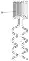
图2为本发明实施例中电极层的结构示意图;2 is a schematic structural diagram of an electrode layer in an embodiment of the present invention;
图3为本发明实施例中施加的脉冲电信号示意图;3 is a schematic diagram of a pulsed electrical signal applied in an embodiment of the present invention;
图4为本发明实施例中电极电场仿真示意图;4 is a schematic diagram of an electrode electric field simulation in an embodiment of the present invention;
图5为本发明实施例的温度传感层中温度敏感金属的结构示意图;5 is a schematic structural diagram of a temperature-sensitive metal in a temperature-sensing layer according to an embodiment of the present invention;
图6为本发明实施例中用于心脏脉冲场消融的MEMS电极器件的制备方法的流程示意图。FIG. 6 is a schematic flowchart of a method for manufacturing a MEMS electrode device for cardiac pulse field ablation according to an embodiment of the present invention.
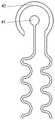
图中:1为下部绝缘层,2为温度传感层,21为温度敏感金属,3为中部绝缘层,4为电极层,41为圆形电极,42为环形电极,5为上部绝缘层,6为电极修饰层;A表示电势分布仿真结果,B表示电场强度分布仿真结果。In the figure: 1 is the lower insulating layer, 2 is the temperature sensing layer, 21 is the temperature sensitive metal, 3 is the middle insulating layer, 4 is the electrode layer, 41 is the circular electrode, 42 is the ring electrode, and 5 is the upper insulating layer, 6 is the electrode modification layer; A represents the simulation result of electric potential distribution, and B represents the simulation result of electric field intensity distribution.
具体实施方式Detailed ways
下面结合具体实施例对本发明进行详细说明。以下实施例将有助于本领域的技术人员进一步理解本发明,但不以任何形式限制本发明。应当指出的是,对本领域的普通技术人员来说,在不脱离本发明构思的前提下,还可以做出若干变形和改进。这些都属于本发明的保护范围。在本发明实施例的描述中,需要说明的是,本发明的说明书和权利要求书及上述附图中的术语“第一”、“第二”等是用于区别类似的对象,而不必用于描述特定的顺序或先后次序。应该理解这样使用的数据在适当情况下可以互换,以便这里描述的本发明的实施例能够以除了在这里图示或描述的那些以外的顺序实施。The present invention will be described in detail below with reference to specific embodiments. The following examples will help those skilled in the art to further understand the present invention, but do not limit the present invention in any form. It should be noted that, for those skilled in the art, several modifications and improvements can be made without departing from the concept of the present invention. These all belong to the protection scope of the present invention. In the description of the embodiments of the present invention, it should be noted that the terms "first" and "second" in the description and claims of the present invention and the above-mentioned drawings are used to distinguish similar objects, and are not necessarily used to describe a specific order or sequence. It is to be understood that the data so used may be interchanged under appropriate circumstances such that the embodiments of the invention described herein can be practiced in sequences other than those illustrated or described herein.
本发明实施例提供一种用于心脏脉冲场消融的MEMS电极器件,参照图1,该器件包括由下至上依次设置的下部绝缘层1、温度传感层2、中部绝缘层3、电极层4、上部绝缘层5和电极修饰层6;其中,电极修饰层6用于降低电极的电化学阻抗并提高电荷储存能力;电极层4用于向心脏组织施加脉冲电信号,并使得心肌细胞发生不可逆电穿孔,同时记录心脏组织在每次脉冲场消融前后的电学阻抗,还用于记录心脏组织在消融前后的心电信号,用于评估消融效果;温度传感层2用于原位记录消融过程中的动态温度变化,以获得最佳的消融参数。An embodiment of the present invention provides a MEMS electrode device for cardiac pulse field ablation. Referring to FIG. 1 , the device includes a lower insulating
本发明实施例中的电极器件能够用于心脏脉冲场消融,并具有阻抗检测功能和心电信号记录功能,以评估消融效果,温度传感层2能够原位精确测温;本发明能够提高心脏脉冲场消融的安全性和效率。The electrode device in the embodiment of the present invention can be used for cardiac pulse field ablation, and has an impedance detection function and an ECG signal recording function to evaluate the ablation effect, and the
参照图2,在一些优选的实施例中,电极层4包括位于中心的圆形电极41和位于圆形电极41周围的环形电极42,圆形电极41与环形电极42形成中心放射状的电场,从而将能量限制在电极所处范围内,这个结构可对心脏组织进行精确的点状消融。电极层4还包括电极层引线,电极层引线分别连接圆形电极41和环形电极42,优选地,电极层引线呈蜿蜒状,以防止器件变形过程中引线容易发生断裂。2, in some preferred embodiments, the
电极层4的材料需具有良好的生物相容性,电极层4的厚度需在MEMS工艺可加工范围内,在一些优选的实施例中,电极层4的材料为金、铂或碳等,厚度为100-500nm。圆形电极41的半径、环形电极42的内半径和外半径均根据设计的单次消融点的大小设置,以保证得到大小精确的消融点尺寸。优选地,圆形电极41的半径为50-500μm;环形电极42的内半径为100-1000μm,外半径为150-1500μm;圆形电极41的圆周与环形电极42的内环圆周之间的距离小于1mm,电极的小间距可实现低电压脉冲场消融,实现施加低电压即可形成脉冲场消融所需达到的高电场强度。The material of the
圆形电极41和环形电极42分别用于与传递脉冲电信号的两个电极即阳极和阴极连接。施加在电极器件上的脉冲电信号满足以下条件:脉冲波形(即脉冲电压信号的形状)为单极脉冲方波或双极脉冲方波;电压(即脉冲电压信号的峰值)为10-500V,用于实现低电压脉冲场消融;脉冲宽度(即每个脉冲的持续时间)为1-100μs;脉冲频率(即脉冲电压信号的重复频率)为1-10Hz;脉冲个数(即每个消融位置施加的脉冲个数)为50-120个。The
优选地,参照图3,为施加的脉冲电信号示意图,满足以下条件:脉冲波形,为单极脉冲方波;电压为100V;脉冲宽度为100μs;脉冲频率为1Hz;脉冲个数为99个。Preferably, referring to FIG. 3, it is a schematic diagram of the applied pulse electrical signal, which meets the following conditions: the pulse waveform is a unipolar pulse square wave; the voltage is 100V; the pulse width is 100μs; the pulse frequency is 1Hz; and the number of pulses is 99.
参照图4,为电极电场仿真图,位于中心的圆形电极41和位于周围的环形电极42施加脉冲电信号后,电势分布仿真结果A和电场强度分布仿真结果B显示二者可形成中心放射状的电场,从而将能量限制在电极所处范围内,这个结构可对心脏组织进行精确的点状消融。Referring to FIG. 4 , which is an electrode electric field simulation diagram, after the
在一些优选的实施例中,参照图5,温度传感层2包括呈蜿蜒状(即蛇形线状)的温度敏感金属21,以实现在有限的面积内增大其有效长度,从而得到更大的电阻变化量。温度敏感金属21采用铂或金等电阻温度系数较大的金属,以获得较大的灵敏度。温度传感层2还包括自温度敏感金属21引出的温度传感层引线,优选地,温度传感层引线呈蜿蜒状(即蛇形线状),以防止器件变形过程中引线容易发生断裂。温度传感层2的厚度为100-500nm,温度传感层2的厚度过小容易发生断裂而断路,厚度过大则减小了其电阻值。温度传感层2与电极层4在电极端上下堆叠设置,电极端和引线端分别位于温度传感层2或电极层4的两端;优选地,温度传感层2与电极层3的圆形电极41和环形电极42形成的端部进行位置的上下堆叠,二者之间仅由中部绝缘层3隔离,以实现温度的原位精确测量。In some preferred embodiments, referring to FIG. 5 , the
在一些优选的实施例中,电极修饰层6采用电镀方式形成,电极修饰层6的材料为铂黑、氧化铱和聚乙烯二氧噻吩-聚苯乙烯磺酸中的任意一种,优选地为铂黑,以降低电极的电化学阻抗并提高电荷储存能力。In some preferred embodiments, the
为保证电极整体具有柔性,在一些优选的实施例中,下部绝缘层1、中部绝缘层3和上部绝缘层5采用同一种材料形成,采用同一种材料加工时比较方便,并且同种材料的兼容性好,相互之间的结合力和密封性好,绝缘层的材料为聚对二甲苯(Parylene)、聚酰亚胺(Polyimide)或SU-8光刻胶等生物相容性材料,下部绝缘层1、中部绝缘层3和上部绝缘层5的厚度为1-200μm,绝缘层的厚度太小则器件容易断裂,厚度太大则器件的柔性降低。本发明实施例中的电极器件整体为柔性,可直接贴附于心脏表面,也可使用生物胶水贴附于医用导管端部借助介入手术进行消融。In order to ensure the flexibility of the electrode as a whole, in some preferred embodiments, the lower insulating
本发明实施例还提供一种上述的用于心脏脉冲场消融的MEMS电极器件的制备方法,该方法包括:Embodiments of the present invention also provide a method for preparing the above-mentioned MEMS electrode device for cardiac pulse field ablation, the method comprising:
S1、在基底上制作下部绝缘层;S1, making a lower insulating layer on the substrate;
S2、在下部绝缘层上溅射一层黏附层,黏附层的材料可以为钛或铬,再溅射第一金属层,采用光刻光刻胶方式对第一金属层进行图形化,具体地,旋涂光刻胶,经过光刻对光刻胶图形化,使用湿法刻蚀或干法刻蚀对金属层进行图形化,形成温度传感层引线;S2, sputtering a layer of adhesion layer on the lower insulating layer, the material of the adhesion layer can be titanium or chromium, and then sputtering the first metal layer, and patterning the first metal layer by photolithography photoresist, specifically , spin coating photoresist, pattern the photoresist by photolithography, pattern the metal layer by wet etching or dry etching, and form the temperature sensing layer leads;
S3、在温度传感层引线上方,采用光刻光刻胶方式形成温度传感层中温度敏感金属的轮廓;S3, above the lead wire of the temperature sensing layer, the outline of the temperature-sensitive metal in the temperature-sensing layer is formed by means of photolithography and photoresist;
S4、溅射一层黏附层,黏附层的材料可以为钛或铬,再溅射温度敏感金属;S4, sputtering a layer of adhesion layer, the material of the adhesion layer can be titanium or chromium, and then sputtering temperature-sensitive metal;
S5、去除光刻胶,留下具有指定轮廓的温度敏感金属,具体地,在热丙酮中浸泡,并经超声振动去除光刻胶,形成温度传感层;S5, removing the photoresist, leaving a temperature-sensitive metal with a specified profile, specifically, soaking in hot acetone, and removing the photoresist by ultrasonic vibration to form a temperature sensing layer;
S6、在温度传感层上方制作中部绝缘层;S6, making a middle insulating layer above the temperature sensing layer;
S7、在中部绝缘层上溅射一层黏附层,黏附层的材料可以为钛或铬,再溅射第二金属层,采用光刻光刻胶方式对第二金属层进行图形化,具体地,旋涂光刻胶,经过光刻对光刻胶图形化,使用湿法刻蚀或干法刻蚀对金属层进行图形化,形成电极层;S7, sputtering a layer of adhesion layer on the middle insulating layer, the material of the adhesion layer can be titanium or chromium, and then sputtering the second metal layer, and patterning the second metal layer by means of photoresist, specifically , spin coating photoresist, pattern the photoresist by photolithography, pattern the metal layer by wet etching or dry etching, and form the electrode layer;
S8、在电极层上制作上部绝缘层;S8, making the upper insulating layer on the electrode layer;
S9、旋涂光刻胶,经过光刻对光刻胶图形化,使用干法刻蚀方法刻蚀并暴露电极部分、焊盘部分和电极器件整体轮廓;S9, spin coating the photoresist, pattern the photoresist by photolithography, and use the dry etching method to etch and expose the electrode part, the pad part and the overall outline of the electrode device;
S10、释放电极器件。S10, releasing the electrode device.
优选地,参照图6,用于心脏脉冲场消融的MEMS电极器件的制备方法包括如下步骤:Preferably, referring to FIG. 6 , a method for preparing a MEMS electrode device for cardiac pulse field ablation includes the following steps:
S1、如图6中(a)所示,在4英寸硅片上,利用化学气相沉积法沉积得到5μm厚的聚对二甲苯(Parylene-C),作为下部绝缘层;S1. As shown in (a) of Figure 6, on a 4-inch silicon wafer, a 5-μm-thick Parylene-C is deposited by chemical vapor deposition as the lower insulating layer;
S2、如图6中(b)所示,在下部绝缘层上溅射一层20nm厚的铬作为黏附层,再溅射400nm厚的金;如图6中(c)所示,旋涂光刻胶,经过光刻对光刻胶图形化,使用湿法刻蚀对铬/金进行图形化,形成温度传感层引线;S2. As shown in Fig. 6(b), sputter a layer of 20nm thick chromium on the lower insulating layer as an adhesion layer, and then sputter 400nm thick gold; as shown in Fig. 6(c), spin coating light The photoresist is patterned by photolithography, and the chromium/gold is patterned by wet etching to form the temperature sensing layer leads;
S3、如图6中(d)所示,旋涂光刻胶,经过光刻对光刻胶图形化,以形成温度传感层中温度敏感金属的轮廓;S3, as shown in (d) in FIG. 6, spin-coating the photoresist, and patterning the photoresist through photolithography to form the profile of the temperature-sensitive metal in the temperature-sensing layer;
S4、如图6中(e)所示,溅射一层20nm厚的铬作为黏附层,再溅射400nm厚的铂,作为温度敏感的金属;S4. As shown in (e) of Figure 6, sputter a layer of 20nm thick chromium as an adhesion layer, and then sputter 400nm thick platinum as a temperature-sensitive metal;
S5、如图6中(f)所示,在热丙酮中浸泡,并经超声振动去除光刻胶,留下具有特定轮廓的温度敏感金属铂;S5, as shown in (f) of Figure 6, soaking in hot acetone, and removing the photoresist by ultrasonic vibration, leaving a temperature-sensitive metal platinum with a specific profile;
S6、如图6中(g)所示,利用化学气相沉积法沉积得到5μm厚的聚对二甲苯(Parylene-C),作为中部绝缘层;S6. As shown in (g) of FIG. 6, a 5 μm-thick Parylene-C is deposited by chemical vapor deposition as the middle insulating layer;
S7、如图6中(h)所示,在中部绝缘层上溅射一层20nm厚的铬作为黏附层,再溅射400nm厚的金;如图6中(i)所示,旋涂光刻胶,经过光刻对光刻胶图形化,使用湿法刻蚀对金进行图形化,形成电极层;S7. As shown in Fig. 6(h), sputter a layer of 20nm thick chromium on the middle insulating layer as an adhesion layer, and then sputter 400nm thick gold; as shown in Fig. 6(i), spin coating light The photoresist is patterned by photolithography, and the gold is patterned by wet etching to form an electrode layer;
S8、如图6中(j)所示,利用化学气相沉积法沉积得到5μm厚的聚对二甲苯(Parylene-C),作为上部绝缘层;S8. As shown in (j) of FIG. 6, a 5 μm thick Parylene-C is deposited by chemical vapor deposition as the upper insulating layer;
S9、如图6中(k)所示,旋涂光刻胶,经过光刻对光刻胶图形化;如图6中(l)所示,使用反应离子刻蚀方法刻蚀并暴露电极部分、焊盘部分和电极器件整体轮廓;S9, as shown in FIG. 6(k), spin-coating the photoresist, and pattern the photoresist through photolithography; as shown in FIG. 6(l), use the reactive ion etching method to etch and expose the electrode portion , the pad part and the overall outline of the electrode device;
S10、如图6中(m)所示,释放电极器件。S10 , as shown in (m) in FIG. 6 , the electrode device is released.
本发明上述实施例中的用于心脏脉冲场消融的MEMS电极器件及其制备方法,利用MEMS技术加工,可在较低电压下用于心脏脉冲场消融,并具有阻抗检测功能和心电信号记录功能,以评估消融效果,温度传感层能够原位精确测温;本发明能够提高心脏脉冲场消融的安全性和效率。The MEMS electrode device for cardiac pulse field ablation in the above-mentioned embodiments of the present invention and the preparation method thereof can be processed by MEMS technology, can be used for cardiac pulse field ablation under lower voltage, and have the function of impedance detection and ECG signal recording function to evaluate the ablation effect, the temperature sensing layer can accurately measure the temperature in situ; the invention can improve the safety and efficiency of cardiac pulse field ablation.
以上对本发明的具体实施例进行了描述。需要理解的是,本发明并不局限于上述特定实施方式,本领域技术人员可以在权利要求的范围内做出各种变形或修改,这并不影响本发明的实质内容。上述各优选特征在互不冲突的情况下,可以任意组合使用。Specific embodiments of the present invention have been described above. It should be understood that the present invention is not limited to the above-mentioned specific embodiments, and those skilled in the art can make various variations or modifications within the scope of the claims, which do not affect the essential content of the present invention. The above-mentioned preferred features can be used in any combination as long as they do not conflict with each other.
Claims (10)
Translated fromChinesePriority Applications (1)
| Application Number | Priority Date | Filing Date | Title |
|---|---|---|---|
| CN202210422714.6ACN114852947B (en) | 2022-04-21 | 2022-04-21 | MEMS electrode device for heart pulse field ablation and preparation method thereof |
Applications Claiming Priority (1)
| Application Number | Priority Date | Filing Date | Title |
|---|---|---|---|
| CN202210422714.6ACN114852947B (en) | 2022-04-21 | 2022-04-21 | MEMS electrode device for heart pulse field ablation and preparation method thereof |
Publications (2)
| Publication Number | Publication Date |
|---|---|
| CN114852947Atrue CN114852947A (en) | 2022-08-05 |
| CN114852947B CN114852947B (en) | 2024-12-17 |
Family
ID=82632037
Family Applications (1)
| Application Number | Title | Priority Date | Filing Date |
|---|---|---|---|
| CN202210422714.6AActiveCN114852947B (en) | 2022-04-21 | 2022-04-21 | MEMS electrode device for heart pulse field ablation and preparation method thereof |
Country Status (1)
| Country | Link |
|---|---|
| CN (1) | CN114852947B (en) |
Cited By (2)
| Publication number | Priority date | Publication date | Assignee | Title |
|---|---|---|---|---|
| CN115568938A (en)* | 2022-09-28 | 2023-01-06 | 上海交通大学 | Fractal structure microelectrode, preparation method thereof and catheter |
| US12076071B2 (en) | 2020-08-14 | 2024-09-03 | Kardium Inc. | Systems and methods for treating tissue with pulsed field ablation |
Citations (8)
| Publication number | Priority date | Publication date | Assignee | Title |
|---|---|---|---|---|
| US20060089637A1 (en)* | 2004-10-14 | 2006-04-27 | Werneth Randell L | Ablation catheter |
| US20120265069A1 (en)* | 2011-04-13 | 2012-10-18 | St. Jude Medical, Inc. | Acoustic transducer for pulse-echo monitoring and control of thermally ablative lesioning in layered and nonlayered tissues, catheter contact monitoring, tissue thickness measurement and pre-pop warning |
| US20160113712A1 (en)* | 2014-10-24 | 2016-04-28 | Boston Scientific Scimed Inc. | Medical devices with a flexible electrode assembly coupled to an ablation tip |
| CN106999151A (en)* | 2014-11-25 | 2017-08-01 | 皇家飞利浦有限公司 | ultrasonic system and method |
| CN112932648A (en)* | 2021-04-07 | 2021-06-11 | 上海宏桐实业有限公司 | Method for improving electroporation effect and preheating pulse ablation system |
| CN113017819A (en)* | 2019-12-24 | 2021-06-25 | 深圳市赛诺思医疗科技有限公司 | Pulse ablation device |
| CN113768616A (en)* | 2021-10-20 | 2021-12-10 | 四川锦江电子科技有限公司 | Integrated system for cardiac ablation |
| CN114052890A (en)* | 2020-08-07 | 2022-02-18 | 上海微创电生理医疗科技股份有限公司 | Impulse ablation device, system, parameter setting method and readable storage medium |
- 2022
- 2022-04-21CNCN202210422714.6Apatent/CN114852947B/enactiveActive
Patent Citations (8)
| Publication number | Priority date | Publication date | Assignee | Title |
|---|---|---|---|---|
| US20060089637A1 (en)* | 2004-10-14 | 2006-04-27 | Werneth Randell L | Ablation catheter |
| US20120265069A1 (en)* | 2011-04-13 | 2012-10-18 | St. Jude Medical, Inc. | Acoustic transducer for pulse-echo monitoring and control of thermally ablative lesioning in layered and nonlayered tissues, catheter contact monitoring, tissue thickness measurement and pre-pop warning |
| US20160113712A1 (en)* | 2014-10-24 | 2016-04-28 | Boston Scientific Scimed Inc. | Medical devices with a flexible electrode assembly coupled to an ablation tip |
| CN106999151A (en)* | 2014-11-25 | 2017-08-01 | 皇家飞利浦有限公司 | ultrasonic system and method |
| CN113017819A (en)* | 2019-12-24 | 2021-06-25 | 深圳市赛诺思医疗科技有限公司 | Pulse ablation device |
| CN114052890A (en)* | 2020-08-07 | 2022-02-18 | 上海微创电生理医疗科技股份有限公司 | Impulse ablation device, system, parameter setting method and readable storage medium |
| CN112932648A (en)* | 2021-04-07 | 2021-06-11 | 上海宏桐实业有限公司 | Method for improving electroporation effect and preheating pulse ablation system |
| CN113768616A (en)* | 2021-10-20 | 2021-12-10 | 四川锦江电子科技有限公司 | Integrated system for cardiac ablation |
Non-Patent Citations (3)
| Title |
|---|
| MENGFEI XU等: "FRACTAL MICROELECTRODES INTEGRATED WITH THE CATHETER FOR LOW-VOLTAGE PULSED FIELD ABLATION", 2023 IEEE 36TH INTERNATIONAL CONFERENCE ON MICRO ELECTRO MECHANICAL SYSTEMS, 3 June 2023 (2023-06-03), pages 405 - 408* |
| 余锂镭等: "脉冲电场消融治疗阵发性心房颤动的初步临床应用", 中国心脏起搏与心电生理杂志, vol. 35, no. 5, 25 October 2021 (2021-10-25), pages 434 - 438* |
| 唐龙军等: "用于心血管介入治疗的柔性MEMS电化学阻抗传感器", 中国科技论文, vol. 12, no. 8, 30 April 2017 (2017-04-30), pages 957 - 961* |
Cited By (2)
| Publication number | Priority date | Publication date | Assignee | Title |
|---|---|---|---|---|
| US12076071B2 (en) | 2020-08-14 | 2024-09-03 | Kardium Inc. | Systems and methods for treating tissue with pulsed field ablation |
| CN115568938A (en)* | 2022-09-28 | 2023-01-06 | 上海交通大学 | Fractal structure microelectrode, preparation method thereof and catheter |
Also Published As
| Publication number | Publication date |
|---|---|
| CN114852947B (en) | 2024-12-17 |
Similar Documents
| Publication | Publication Date | Title |
|---|---|---|
| US12138059B2 (en) | Masked ring electrodes | |
| US12102436B2 (en) | Electrophysiology catheter design | |
| CN112135576B (en) | Radiofrequency ablation and direct current electroporation catheters | |
| CN111836579B (en) | Variable density mapping catheter | |
| EP3151773B1 (en) | Electrode assembly | |
| CN114852947A (en) | MEMS electrode device for cardiac pulse field ablation and preparation method thereof | |
| KR101490374B1 (en) | High resolution electrophysiology catheter | |
| JPH06507797A (en) | Single-phase action potential/ablation combination catheter and high-performance filter system | |
| CN108751116A (en) | Warpage type flexible electrode and preparation method thereof for biological electrographic recording or electro photoluminescence | |
| US10758144B2 (en) | Flexible electrode for cardiac sensing and method for making | |
| WO2004034899A2 (en) | Transseptal access tissue thickness sensing dilator devices and methods for fabricating and using same | |
| CN107485386B (en) | Intracranial cortex nerve information detection electrode, electrode array and preparation method thereof | |
| CN105873507A (en) | Medical devices for mapping cardiac tissue | |
| US20130190586A1 (en) | Multi-Terminal Nanoelectrode Array | |
| CN115568938A (en) | Fractal structure microelectrode, preparation method thereof and catheter | |
| Xu et al. | A High‐Precision, Low‐Voltage Pulsed Field Ablation Device with Capability of Minimally Invasive Surgery | |
| CN112353484B (en) | A flexible microsensor system, extensible flexible device and preparation method | |
| Xu et al. | Fractal microelectrodes integrated with the catheter for low-voltage pulsed field ablation | |
| Xu et al. | Low-voltage flexible interdigital electrode for pulsed field ablation with effect evaluation | |
| CN117503318A (en) | MEMS device and preparation method for irreversible electroporation treatment of cardiac tissue | |
| Xu et al. | Multimodal MEMS Microwrinkle Electronics for Cardiac Pulsed Field Ablation and Sensing | |
| JPH01204647A (en) | Sticking needle | |
| TW202317037A (en) | Magnetic field compatible neural probe and manufacturing method thereof | |
| CN118303971A (en) | AF-based atrial fibrillation catheter ablation method and system |
Legal Events
| Date | Code | Title | Description |
|---|---|---|---|
| PB01 | Publication | ||
| PB01 | Publication | ||
| SE01 | Entry into force of request for substantive examination | ||
| SE01 | Entry into force of request for substantive examination | ||
| GR01 | Patent grant | ||
| GR01 | Patent grant |