CN114823494A - Interconnect structure and method of forming the same - Google Patents
Interconnect structure and method of forming the sameDownload PDFInfo
- Publication number
- CN114823494A CN114823494ACN202110737821.3ACN202110737821ACN114823494ACN 114823494 ACN114823494 ACN 114823494ACN 202110737821 ACN202110737821 ACN 202110737821ACN 114823494 ACN114823494 ACN 114823494A
- Authority
- CN
- China
- Prior art keywords
- layer
- conductive
- liner
- forming
- conductive feature
- Prior art date
- Legal status (The legal status is an assumption and is not a legal conclusion. Google has not performed a legal analysis and makes no representation as to the accuracy of the status listed.)
- Pending
Links
- 238000000034methodMethods0.000titleclaimsabstractdescription129
- 230000004888barrier functionEffects0.000claimsabstractdescription104
- 230000008569processEffects0.000claimsabstractdescription65
- 229910052707rutheniumInorganic materials0.000claimsabstractdescription43
- KJTLSVCANCCWHF-UHFFFAOYSA-NRutheniumChemical compound[Ru]KJTLSVCANCCWHF-UHFFFAOYSA-N0.000claimsabstractdescription39
- 239000004020conductorSubstances0.000claimsabstractdescription23
- 238000004519manufacturing processMethods0.000claimsabstractdescription17
- 239000004065semiconductorSubstances0.000claimsdescription37
- 238000009832plasma treatmentMethods0.000claimsdescription31
- 229910017052cobaltInorganic materials0.000claimsdescription27
- 239000010941cobaltSubstances0.000claimsdescription27
- GUTLYIVDDKVIGB-UHFFFAOYSA-Ncobalt atomChemical compound[Co]GUTLYIVDDKVIGB-UHFFFAOYSA-N0.000claimsdescription27
- 238000000151depositionMethods0.000claimsdescription23
- 229910052739hydrogenInorganic materials0.000claimsdescription14
- UFHFLCQGNIYNRP-UHFFFAOYSA-NHydrogenChemical compound[H][H]UFHFLCQGNIYNRP-UHFFFAOYSA-N0.000claimsdescription13
- 239000001257hydrogenSubstances0.000claimsdescription13
- 239000002131composite materialSubstances0.000claimsdescription9
- 238000011049fillingMethods0.000abstractdescription12
- 239000010410layerSubstances0.000description421
- 239000000463materialSubstances0.000description56
- 229910052751metalInorganic materials0.000description22
- 239000002184metalSubstances0.000description22
- 238000005530etchingMethods0.000description19
- 239000000758substrateSubstances0.000description19
- 239000010949copperSubstances0.000description17
- 125000006850spacer groupChemical group0.000description17
- 239000003989dielectric materialSubstances0.000description16
- 229910052802copperInorganic materials0.000description15
- 238000000231atomic layer depositionMethods0.000description12
- RYGMFSIKBFXOCR-UHFFFAOYSA-NCopperChemical compound[Cu]RYGMFSIKBFXOCR-UHFFFAOYSA-N0.000description10
- 230000007797corrosionEffects0.000description9
- 238000005260corrosionMethods0.000description9
- 150000002739metalsChemical class0.000description9
- 238000000623plasma-assisted chemical vapour depositionMethods0.000description9
- VYPSYNLAJGMNEJ-UHFFFAOYSA-NSilicium dioxideChemical compoundO=[Si]=OVYPSYNLAJGMNEJ-UHFFFAOYSA-N0.000description7
- 230000008021depositionEffects0.000description7
- 238000009792diffusion processMethods0.000description7
- 239000012535impuritySubstances0.000description7
- 238000005240physical vapour depositionMethods0.000description7
- 229910052710siliconInorganic materials0.000description7
- 229910052814silicon oxideInorganic materials0.000description7
- XUIMIQQOPSSXEZ-UHFFFAOYSA-NSiliconChemical compound[Si]XUIMIQQOPSSXEZ-UHFFFAOYSA-N0.000description6
- 229910045601alloyInorganic materials0.000description6
- 239000000956alloySubstances0.000description6
- QRUDEWIWKLJBPS-UHFFFAOYSA-NbenzotriazoleChemical compoundC1=CC=C2N[N][N]C2=C1QRUDEWIWKLJBPS-UHFFFAOYSA-N0.000description6
- 239000012964benzotriazoleSubstances0.000description6
- 238000000059patterningMethods0.000description6
- 238000012545processingMethods0.000description6
- 239000010703siliconSubstances0.000description6
- 229910052719titaniumInorganic materials0.000description6
- 239000010936titaniumSubstances0.000description6
- 229910052581Si3N4Inorganic materials0.000description5
- -1TaAlCInorganic materials0.000description5
- 229910052782aluminiumInorganic materials0.000description5
- 238000013459approachMethods0.000description5
- 239000012212insulatorSubstances0.000description5
- 238000000206photolithographyMethods0.000description5
- 238000000926separation methodMethods0.000description5
- HQVNEWCFYHHQES-UHFFFAOYSA-Nsilicon nitrideChemical compoundN12[Si]34N5[Si]62N3[Si]51N64HQVNEWCFYHHQES-UHFFFAOYSA-N0.000description5
- ATJFFYVFTNAWJD-UHFFFAOYSA-NTinChemical compound[Sn]ATJFFYVFTNAWJD-UHFFFAOYSA-N0.000description4
- 230000008901benefitEffects0.000description4
- 238000001020plasma etchingMethods0.000description4
- 239000002243precursorSubstances0.000description4
- 229910010271silicon carbideInorganic materials0.000description4
- HBMJWWWQQXIZIP-UHFFFAOYSA-Nsilicon carbideChemical compound[Si+]#[C-]HBMJWWWQQXIZIP-UHFFFAOYSA-N0.000description4
- 229910052718tinInorganic materials0.000description4
- 125000004429atomChemical group0.000description3
- 230000009286beneficial effectEffects0.000description3
- 230000015572biosynthetic processEffects0.000description3
- 238000006243chemical reactionMethods0.000description3
- 238000007772electroless platingMethods0.000description3
- 238000001459lithographyMethods0.000description3
- 239000002135nanosheetSubstances0.000description3
- 239000002070nanowireSubstances0.000description3
- 239000005360phosphosilicate glassSubstances0.000description3
- 238000007747platingMethods0.000description3
- 238000004528spin coatingMethods0.000description3
- 229910052721tungstenInorganic materials0.000description3
- 229910017107AlOxInorganic materials0.000description2
- KAKZBPTYRLMSJV-UHFFFAOYSA-NButadieneChemical compoundC=CC=CKAKZBPTYRLMSJV-UHFFFAOYSA-N0.000description2
- JUJWROOIHBZHMG-UHFFFAOYSA-NPyridineChemical compoundC1=CC=NC=C1JUJWROOIHBZHMG-UHFFFAOYSA-N0.000description2
- 229910020286SiOxNyInorganic materials0.000description2
- 229910000577Silicon-germaniumInorganic materials0.000description2
- 229910004166TaNInorganic materials0.000description2
- GWEVSGVZZGPLCZ-UHFFFAOYSA-NTitan oxideChemical compoundO=[Ti]=OGWEVSGVZZGPLCZ-UHFFFAOYSA-N0.000description2
- XLOMVQKBTHCTTD-UHFFFAOYSA-NZinc monoxideChemical compound[Zn]=OXLOMVQKBTHCTTD-UHFFFAOYSA-N0.000description2
- 229910003134ZrOxInorganic materials0.000description2
- LEVVHYCKPQWKOP-UHFFFAOYSA-N[Si].[Ge]Chemical compound[Si].[Ge]LEVVHYCKPQWKOP-UHFFFAOYSA-N0.000description2
- 125000005605benzo groupChemical group0.000description2
- 229910052796boronInorganic materials0.000description2
- 239000005388borosilicate glassSubstances0.000description2
- 229910052799carbonInorganic materials0.000description2
- 238000005137deposition processMethods0.000description2
- 238000013461designMethods0.000description2
- 239000002019doping agentSubstances0.000description2
- 238000001312dry etchingMethods0.000description2
- 238000002149energy-dispersive X-ray emission spectroscopyMethods0.000description2
- 239000007789gasSubstances0.000description2
- 229910052732germaniumInorganic materials0.000description2
- 238000011065in-situ storageMethods0.000description2
- 230000010354integrationEffects0.000description2
- 238000005468ion implantationMethods0.000description2
- 238000002955isolationMethods0.000description2
- 238000004943liquid phase epitaxyMethods0.000description2
- 238000004518low pressure chemical vapour depositionMethods0.000description2
- 238000002156mixingMethods0.000description2
- 229910052750molybdenumInorganic materials0.000description2
- 229910052759nickelInorganic materials0.000description2
- 229910052757nitrogenInorganic materials0.000description2
- 229910052760oxygenInorganic materials0.000description2
- 238000006479redox reactionMethods0.000description2
- 150000004760silicatesChemical class0.000description2
- 229910052715tantalumInorganic materials0.000description2
- XOLBLPGZBRYERU-UHFFFAOYSA-Ntin dioxideChemical compoundO=[Sn]=OXOLBLPGZBRYERU-UHFFFAOYSA-N0.000description2
- 229910052726zirconiumInorganic materials0.000description2
- GWYPDXLJACEENP-UHFFFAOYSA-N1,3-cycloheptadieneChemical compoundC1CC=CC=CC1GWYPDXLJACEENP-UHFFFAOYSA-N0.000description1
- ITWBWJFEJCHKSN-UHFFFAOYSA-N1,4,7-triazonaneChemical compoundC1CNCCNCCN1ITWBWJFEJCHKSN-UHFFFAOYSA-N0.000description1
- 229910017083AlNInorganic materials0.000description1
- ZOXJGFHDIHLPTG-UHFFFAOYSA-NBoronChemical compound[B]ZOXJGFHDIHLPTG-UHFFFAOYSA-N0.000description1
- OKTJSMMVPCPJKN-UHFFFAOYSA-NCarbonChemical compound[C]OKTJSMMVPCPJKN-UHFFFAOYSA-N0.000description1
- 229910005191Ga 2 O 3Inorganic materials0.000description1
- 229910001218Gallium arsenideInorganic materials0.000description1
- 229910000673Indium arsenideInorganic materials0.000description1
- ZOKXTWBITQBERF-UHFFFAOYSA-NMolybdenumChemical compound[Mo]ZOKXTWBITQBERF-UHFFFAOYSA-N0.000description1
- BPQQTUXANYXVAA-UHFFFAOYSA-NOrthosilicateChemical compound[O-][Si]([O-])([O-])[O-]BPQQTUXANYXVAA-UHFFFAOYSA-N0.000description1
- 229910004541SiNInorganic materials0.000description1
- 229910004490TaAlInorganic materials0.000description1
- 229910004200TaSiNInorganic materials0.000description1
- 229910010037TiAlNInorganic materials0.000description1
- RTAQQCXQSZGOHL-UHFFFAOYSA-NTitaniumChemical compound[Ti]RTAQQCXQSZGOHL-UHFFFAOYSA-N0.000description1
- NRTOMJZYCJJWKI-UHFFFAOYSA-NTitanium nitrideChemical compound[Ti]#NNRTOMJZYCJJWKI-UHFFFAOYSA-N0.000description1
- 239000004964aerogelSubstances0.000description1
- 125000000217alkyl groupChemical group0.000description1
- 230000004075alterationEffects0.000description1
- 229910021417amorphous siliconInorganic materials0.000description1
- 238000000137annealingMethods0.000description1
- 229910052785arsenicInorganic materials0.000description1
- 238000000277atomic layer chemical vapour depositionMethods0.000description1
- QVGXLLKOCUKJST-UHFFFAOYSA-Natomic oxygenChemical compound[O]QVGXLLKOCUKJST-UHFFFAOYSA-N0.000description1
- 229910052788bariumInorganic materials0.000description1
- 125000002915carbonyl groupChemical group[*:2]C([*:1])=O0.000description1
- 239000013522chelantSubstances0.000description1
- 238000005229chemical vapour depositionMethods0.000description1
- 238000004140cleaningMethods0.000description1
- 150000001875compoundsChemical class0.000description1
- 239000011231conductive fillerSubstances0.000description1
- 238000010276constructionMethods0.000description1
- 230000007423decreaseEffects0.000description1
- 230000003247decreasing effectEffects0.000description1
- 238000011161developmentMethods0.000description1
- 230000009977dual effectEffects0.000description1
- 238000000407epitaxyMethods0.000description1
- 230000003628erosive effectEffects0.000description1
- 230000005669field effectEffects0.000description1
- 238000005429filling processMethods0.000description1
- 230000009969flowable effectEffects0.000description1
- 229910052731fluorineInorganic materials0.000description1
- 229940104869fluorosilicateDrugs0.000description1
- 125000000524functional groupChemical group0.000description1
- GNPVGFCGXDBREM-UHFFFAOYSA-Ngermanium atomChemical compound[Ge]GNPVGFCGXDBREM-UHFFFAOYSA-N0.000description1
- 239000011521glassSubstances0.000description1
- 229910052735hafniumInorganic materials0.000description1
- AHAREKHAZNPPMI-UHFFFAOYSA-Nhexa-1,3-dieneChemical compoundCCC=CC=CAHAREKHAZNPPMI-UHFFFAOYSA-N0.000description1
- 230000002209hydrophobic effectEffects0.000description1
- 238000007654immersionMethods0.000description1
- 229910052738indiumInorganic materials0.000description1
- RPQDHPTXJYYUPQ-UHFFFAOYSA-Nindium arsenideChemical compound[In]#[As]RPQDHPTXJYYUPQ-UHFFFAOYSA-N0.000description1
- 230000000977initiatory effectEffects0.000description1
- 239000011810insulating materialSubstances0.000description1
- 239000011229interlayerSubstances0.000description1
- 229910052746lanthanumInorganic materials0.000description1
- 229910052749magnesiumInorganic materials0.000description1
- 229910052748manganeseInorganic materials0.000description1
- 229910003465moissaniteInorganic materials0.000description1
- 238000001451molecular beam epitaxyMethods0.000description1
- 239000011733molybdenumSubstances0.000description1
- 239000002086nanomaterialSubstances0.000description1
- 125000004433nitrogen atomChemical groupN*0.000description1
- 230000003647oxidationEffects0.000description1
- 238000007254oxidation reactionMethods0.000description1
- 230000001590oxidative effectEffects0.000description1
- 239000001301oxygenSubstances0.000description1
- 229910052698phosphorusInorganic materials0.000description1
- 229920002120photoresistant polymerPolymers0.000description1
- 229910052697platinumInorganic materials0.000description1
- 238000005498polishingMethods0.000description1
- 229920003209poly(hydridosilsesquioxane)Polymers0.000description1
- 229910021420polycrystalline siliconInorganic materials0.000description1
- 229920005591polysiliconPolymers0.000description1
- UMJSCPRVCHMLSP-UHFFFAOYSA-NpyridineNatural productsCOC1=CC=CN=C1UMJSCPRVCHMLSP-UHFFFAOYSA-N0.000description1
- 230000009467reductionEffects0.000description1
- 230000008439repair processEffects0.000description1
- 229910052703rhodiumInorganic materials0.000description1
- 239000010948rhodiumSubstances0.000description1
- MHOVAHRLVXNVSD-UHFFFAOYSA-Nrhodium atomChemical compound[Rh]MHOVAHRLVXNVSD-UHFFFAOYSA-N0.000description1
- 239000005368silicate glassSubstances0.000description1
- 229910052709silverInorganic materials0.000description1
- 239000002356single layerSubstances0.000description1
- 238000002791soakingMethods0.000description1
- 239000007790solid phaseSubstances0.000description1
- 238000000348solid-phase epitaxyMethods0.000description1
- 239000000126substanceSubstances0.000description1
- 238000006467substitution reactionMethods0.000description1
- GUVRBAGPIYLISA-UHFFFAOYSA-Ntantalum atomChemical compound[Ta]GUVRBAGPIYLISA-UHFFFAOYSA-N0.000description1
- MZLGASXMSKOWSE-UHFFFAOYSA-Ntantalum nitrideChemical compound[Ta]#NMZLGASXMSKOWSE-UHFFFAOYSA-N0.000description1
- 238000007669thermal treatmentMethods0.000description1
- 238000012546transferMethods0.000description1
- 239000012808vapor phaseSubstances0.000description1
- 238000001039wet etchingMethods0.000description1
Images


Classifications
- H—ELECTRICITY
- H01—ELECTRIC ELEMENTS
- H01L—SEMICONDUCTOR DEVICES NOT COVERED BY CLASS H10
- H01L21/00—Processes or apparatus adapted for the manufacture or treatment of semiconductor or solid state devices or of parts thereof
- H01L21/70—Manufacture or treatment of devices consisting of a plurality of solid state components formed in or on a common substrate or of parts thereof; Manufacture of integrated circuit devices or of parts thereof
- H01L21/71—Manufacture of specific parts of devices defined in group H01L21/70
- H01L21/768—Applying interconnections to be used for carrying current between separate components within a device comprising conductors and dielectrics
- H01L21/76838—Applying interconnections to be used for carrying current between separate components within a device comprising conductors and dielectrics characterised by the formation and the after-treatment of the conductors
- H01L21/76841—Barrier, adhesion or liner layers
- H01L21/76843—Barrier, adhesion or liner layers formed in openings in a dielectric
- H01L21/76844—Bottomless liners
- H—ELECTRICITY
- H01—ELECTRIC ELEMENTS
- H01L—SEMICONDUCTOR DEVICES NOT COVERED BY CLASS H10
- H01L21/00—Processes or apparatus adapted for the manufacture or treatment of semiconductor or solid state devices or of parts thereof
- H01L21/70—Manufacture or treatment of devices consisting of a plurality of solid state components formed in or on a common substrate or of parts thereof; Manufacture of integrated circuit devices or of parts thereof
- H01L21/71—Manufacture of specific parts of devices defined in group H01L21/70
- H01L21/768—Applying interconnections to be used for carrying current between separate components within a device comprising conductors and dielectrics
- H01L21/76801—Applying interconnections to be used for carrying current between separate components within a device comprising conductors and dielectrics characterised by the formation and the after-treatment of the dielectrics, e.g. smoothing
- H01L21/76829—Applying interconnections to be used for carrying current between separate components within a device comprising conductors and dielectrics characterised by the formation and the after-treatment of the dielectrics, e.g. smoothing characterised by the formation of thin functional dielectric layers, e.g. dielectric etch-stop, barrier, capping or liner layers
- H01L21/76831—Applying interconnections to be used for carrying current between separate components within a device comprising conductors and dielectrics characterised by the formation and the after-treatment of the dielectrics, e.g. smoothing characterised by the formation of thin functional dielectric layers, e.g. dielectric etch-stop, barrier, capping or liner layers in via holes or trenches, e.g. non-conductive sidewall liners
- H—ELECTRICITY
- H01—ELECTRIC ELEMENTS
- H01L—SEMICONDUCTOR DEVICES NOT COVERED BY CLASS H10
- H01L21/00—Processes or apparatus adapted for the manufacture or treatment of semiconductor or solid state devices or of parts thereof
- H01L21/70—Manufacture or treatment of devices consisting of a plurality of solid state components formed in or on a common substrate or of parts thereof; Manufacture of integrated circuit devices or of parts thereof
- H01L21/71—Manufacture of specific parts of devices defined in group H01L21/70
- H01L21/768—Applying interconnections to be used for carrying current between separate components within a device comprising conductors and dielectrics
- H01L21/76801—Applying interconnections to be used for carrying current between separate components within a device comprising conductors and dielectrics characterised by the formation and the after-treatment of the dielectrics, e.g. smoothing
- H01L21/76802—Applying interconnections to be used for carrying current between separate components within a device comprising conductors and dielectrics characterised by the formation and the after-treatment of the dielectrics, e.g. smoothing by forming openings in dielectrics
- H01L21/76814—Applying interconnections to be used for carrying current between separate components within a device comprising conductors and dielectrics characterised by the formation and the after-treatment of the dielectrics, e.g. smoothing by forming openings in dielectrics post-treatment or after-treatment, e.g. cleaning or removal of oxides on underlying conductors
- H—ELECTRICITY
- H01—ELECTRIC ELEMENTS
- H01L—SEMICONDUCTOR DEVICES NOT COVERED BY CLASS H10
- H01L21/00—Processes or apparatus adapted for the manufacture or treatment of semiconductor or solid state devices or of parts thereof
- H01L21/70—Manufacture or treatment of devices consisting of a plurality of solid state components formed in or on a common substrate or of parts thereof; Manufacture of integrated circuit devices or of parts thereof
- H01L21/71—Manufacture of specific parts of devices defined in group H01L21/70
- H01L21/768—Applying interconnections to be used for carrying current between separate components within a device comprising conductors and dielectrics
- H01L21/76801—Applying interconnections to be used for carrying current between separate components within a device comprising conductors and dielectrics characterised by the formation and the after-treatment of the dielectrics, e.g. smoothing
- H01L21/76829—Applying interconnections to be used for carrying current between separate components within a device comprising conductors and dielectrics characterised by the formation and the after-treatment of the dielectrics, e.g. smoothing characterised by the formation of thin functional dielectric layers, e.g. dielectric etch-stop, barrier, capping or liner layers
- H—ELECTRICITY
- H01—ELECTRIC ELEMENTS
- H01L—SEMICONDUCTOR DEVICES NOT COVERED BY CLASS H10
- H01L21/00—Processes or apparatus adapted for the manufacture or treatment of semiconductor or solid state devices or of parts thereof
- H01L21/70—Manufacture or treatment of devices consisting of a plurality of solid state components formed in or on a common substrate or of parts thereof; Manufacture of integrated circuit devices or of parts thereof
- H01L21/71—Manufacture of specific parts of devices defined in group H01L21/70
- H01L21/768—Applying interconnections to be used for carrying current between separate components within a device comprising conductors and dielectrics
- H01L21/76838—Applying interconnections to be used for carrying current between separate components within a device comprising conductors and dielectrics characterised by the formation and the after-treatment of the conductors
- H01L21/76841—Barrier, adhesion or liner layers
- H01L21/76843—Barrier, adhesion or liner layers formed in openings in a dielectric
- H01L21/76846—Layer combinations
- H—ELECTRICITY
- H01—ELECTRIC ELEMENTS
- H01L—SEMICONDUCTOR DEVICES NOT COVERED BY CLASS H10
- H01L21/00—Processes or apparatus adapted for the manufacture or treatment of semiconductor or solid state devices or of parts thereof
- H01L21/70—Manufacture or treatment of devices consisting of a plurality of solid state components formed in or on a common substrate or of parts thereof; Manufacture of integrated circuit devices or of parts thereof
- H01L21/71—Manufacture of specific parts of devices defined in group H01L21/70
- H01L21/768—Applying interconnections to be used for carrying current between separate components within a device comprising conductors and dielectrics
- H01L21/76838—Applying interconnections to be used for carrying current between separate components within a device comprising conductors and dielectrics characterised by the formation and the after-treatment of the conductors
- H01L21/76841—Barrier, adhesion or liner layers
- H01L21/76843—Barrier, adhesion or liner layers formed in openings in a dielectric
- H01L21/76849—Barrier, adhesion or liner layers formed in openings in a dielectric the layer being positioned on top of the main fill metal
- H—ELECTRICITY
- H01—ELECTRIC ELEMENTS
- H01L—SEMICONDUCTOR DEVICES NOT COVERED BY CLASS H10
- H01L21/00—Processes or apparatus adapted for the manufacture or treatment of semiconductor or solid state devices or of parts thereof
- H01L21/70—Manufacture or treatment of devices consisting of a plurality of solid state components formed in or on a common substrate or of parts thereof; Manufacture of integrated circuit devices or of parts thereof
- H01L21/71—Manufacture of specific parts of devices defined in group H01L21/70
- H01L21/768—Applying interconnections to be used for carrying current between separate components within a device comprising conductors and dielectrics
- H01L21/76838—Applying interconnections to be used for carrying current between separate components within a device comprising conductors and dielectrics characterised by the formation and the after-treatment of the conductors
- H01L21/76841—Barrier, adhesion or liner layers
- H01L21/76853—Barrier, adhesion or liner layers characterized by particular after-treatment steps
- H01L21/76855—After-treatment introducing at least one additional element into the layer
- H01L21/76858—After-treatment introducing at least one additional element into the layer by diffusing alloying elements
- H—ELECTRICITY
- H01—ELECTRIC ELEMENTS
- H01L—SEMICONDUCTOR DEVICES NOT COVERED BY CLASS H10
- H01L21/00—Processes or apparatus adapted for the manufacture or treatment of semiconductor or solid state devices or of parts thereof
- H01L21/70—Manufacture or treatment of devices consisting of a plurality of solid state components formed in or on a common substrate or of parts thereof; Manufacture of integrated circuit devices or of parts thereof
- H01L21/71—Manufacture of specific parts of devices defined in group H01L21/70
- H01L21/768—Applying interconnections to be used for carrying current between separate components within a device comprising conductors and dielectrics
- H01L21/76838—Applying interconnections to be used for carrying current between separate components within a device comprising conductors and dielectrics characterised by the formation and the after-treatment of the conductors
- H01L21/76877—Filling of holes, grooves or trenches, e.g. vias, with conductive material
- H01L21/76883—Post-treatment or after-treatment of the conductive material
- H—ELECTRICITY
- H01—ELECTRIC ELEMENTS
- H01L—SEMICONDUCTOR DEVICES NOT COVERED BY CLASS H10
- H01L23/00—Details of semiconductor or other solid state devices
- H01L23/52—Arrangements for conducting electric current within the device in operation from one component to another, i.e. interconnections, e.g. wires, lead frames
- H01L23/522—Arrangements for conducting electric current within the device in operation from one component to another, i.e. interconnections, e.g. wires, lead frames including external interconnections consisting of a multilayer structure of conductive and insulating layers inseparably formed on the semiconductor body
- H01L23/5226—Via connections in a multilevel interconnection structure
- H—ELECTRICITY
- H01—ELECTRIC ELEMENTS
- H01L—SEMICONDUCTOR DEVICES NOT COVERED BY CLASS H10
- H01L23/00—Details of semiconductor or other solid state devices
- H01L23/52—Arrangements for conducting electric current within the device in operation from one component to another, i.e. interconnections, e.g. wires, lead frames
- H01L23/522—Arrangements for conducting electric current within the device in operation from one component to another, i.e. interconnections, e.g. wires, lead frames including external interconnections consisting of a multilayer structure of conductive and insulating layers inseparably formed on the semiconductor body
- H01L23/528—Layout of the interconnection structure
- H01L23/5283—Cross-sectional geometry
- H—ELECTRICITY
- H01—ELECTRIC ELEMENTS
- H01L—SEMICONDUCTOR DEVICES NOT COVERED BY CLASS H10
- H01L23/00—Details of semiconductor or other solid state devices
- H01L23/52—Arrangements for conducting electric current within the device in operation from one component to another, i.e. interconnections, e.g. wires, lead frames
- H01L23/522—Arrangements for conducting electric current within the device in operation from one component to another, i.e. interconnections, e.g. wires, lead frames including external interconnections consisting of a multilayer structure of conductive and insulating layers inseparably formed on the semiconductor body
- H01L23/532—Arrangements for conducting electric current within the device in operation from one component to another, i.e. interconnections, e.g. wires, lead frames including external interconnections consisting of a multilayer structure of conductive and insulating layers inseparably formed on the semiconductor body characterised by the materials
- H01L23/53204—Conductive materials
- H01L23/53209—Conductive materials based on metals, e.g. alloys, metal silicides
- H01L23/53228—Conductive materials based on metals, e.g. alloys, metal silicides the principal metal being copper
- H01L23/53238—Additional layers associated with copper layers, e.g. adhesion, barrier, cladding layers
- H—ELECTRICITY
- H10—SEMICONDUCTOR DEVICES; ELECTRIC SOLID-STATE DEVICES NOT OTHERWISE PROVIDED FOR
- H10D—INORGANIC ELECTRIC SEMICONDUCTOR DEVICES
- H10D30/00—Field-effect transistors [FET]
- H10D30/01—Manufacture or treatment
- H10D30/014—Manufacture or treatment of FETs having zero-dimensional [0D] or one-dimensional [1D] channels, e.g. quantum wire FETs, single-electron transistors [SET] or Coulomb blockade transistors
- H—ELECTRICITY
- H10—SEMICONDUCTOR DEVICES; ELECTRIC SOLID-STATE DEVICES NOT OTHERWISE PROVIDED FOR
- H10D—INORGANIC ELECTRIC SEMICONDUCTOR DEVICES
- H10D30/00—Field-effect transistors [FET]
- H10D30/01—Manufacture or treatment
- H10D30/021—Manufacture or treatment of FETs having insulated gates [IGFET]
- H10D30/024—Manufacture or treatment of FETs having insulated gates [IGFET] of fin field-effect transistors [FinFET]
- H—ELECTRICITY
- H10—SEMICONDUCTOR DEVICES; ELECTRIC SOLID-STATE DEVICES NOT OTHERWISE PROVIDED FOR
- H10D—INORGANIC ELECTRIC SEMICONDUCTOR DEVICES
- H10D30/00—Field-effect transistors [FET]
- H10D30/01—Manufacture or treatment
- H10D30/021—Manufacture or treatment of FETs having insulated gates [IGFET]
- H10D30/031—Manufacture or treatment of FETs having insulated gates [IGFET] of thin-film transistors [TFT]
- H—ELECTRICITY
- H10—SEMICONDUCTOR DEVICES; ELECTRIC SOLID-STATE DEVICES NOT OTHERWISE PROVIDED FOR
- H10D—INORGANIC ELECTRIC SEMICONDUCTOR DEVICES
- H10D30/00—Field-effect transistors [FET]
- H10D30/60—Insulated-gate field-effect transistors [IGFET]
- H10D30/62—Fin field-effect transistors [FinFET]
- H10D30/6211—Fin field-effect transistors [FinFET] having fin-shaped semiconductor bodies integral with the bulk semiconductor substrates
- H—ELECTRICITY
- H10—SEMICONDUCTOR DEVICES; ELECTRIC SOLID-STATE DEVICES NOT OTHERWISE PROVIDED FOR
- H10D—INORGANIC ELECTRIC SEMICONDUCTOR DEVICES
- H10D30/00—Field-effect transistors [FET]
- H10D30/60—Insulated-gate field-effect transistors [IGFET]
- H10D30/67—Thin-film transistors [TFT]
- H—ELECTRICITY
- H10—SEMICONDUCTOR DEVICES; ELECTRIC SOLID-STATE DEVICES NOT OTHERWISE PROVIDED FOR
- H10D—INORGANIC ELECTRIC SEMICONDUCTOR DEVICES
- H10D30/00—Field-effect transistors [FET]
- H10D30/60—Insulated-gate field-effect transistors [IGFET]
- H10D30/67—Thin-film transistors [TFT]
- H10D30/6729—Thin-film transistors [TFT] characterised by the electrodes
- H10D30/673—Thin-film transistors [TFT] characterised by the electrodes characterised by the shapes, relative sizes or dispositions of the gate electrodes
- H10D30/6735—Thin-film transistors [TFT] characterised by the electrodes characterised by the shapes, relative sizes or dispositions of the gate electrodes having gates fully surrounding the channels, e.g. gate-all-around
- H—ELECTRICITY
- H10—SEMICONDUCTOR DEVICES; ELECTRIC SOLID-STATE DEVICES NOT OTHERWISE PROVIDED FOR
- H10D—INORGANIC ELECTRIC SEMICONDUCTOR DEVICES
- H10D62/00—Semiconductor bodies, or regions thereof, of devices having potential barriers
- H10D62/10—Shapes, relative sizes or dispositions of the regions of the semiconductor bodies; Shapes of the semiconductor bodies
- H10D62/117—Shapes of semiconductor bodies
- H10D62/118—Nanostructure semiconductor bodies
- H10D62/119—Nanowire, nanosheet or nanotube semiconductor bodies
- H10D62/121—Nanowire, nanosheet or nanotube semiconductor bodies oriented parallel to substrates
- H—ELECTRICITY
- H10—SEMICONDUCTOR DEVICES; ELECTRIC SOLID-STATE DEVICES NOT OTHERWISE PROVIDED FOR
- H10D—INORGANIC ELECTRIC SEMICONDUCTOR DEVICES
- H10D62/00—Semiconductor bodies, or regions thereof, of devices having potential barriers
- H10D62/10—Shapes, relative sizes or dispositions of the regions of the semiconductor bodies; Shapes of the semiconductor bodies
- H10D62/117—Shapes of semiconductor bodies
- H10D62/118—Nanostructure semiconductor bodies
- H10D62/119—Nanowire, nanosheet or nanotube semiconductor bodies
- H10D62/122—Nanowire, nanosheet or nanotube semiconductor bodies oriented at angles to substrates, e.g. perpendicular to substrates
- H—ELECTRICITY
- H10—SEMICONDUCTOR DEVICES; ELECTRIC SOLID-STATE DEVICES NOT OTHERWISE PROVIDED FOR
- H10D—INORGANIC ELECTRIC SEMICONDUCTOR DEVICES
- H10D84/00—Integrated devices formed in or on semiconductor substrates that comprise only semiconducting layers, e.g. on Si wafers or on GaAs-on-Si wafers
- H10D84/01—Manufacture or treatment
- H10D84/0123—Integrating together multiple components covered by H10D12/00 or H10D30/00, e.g. integrating multiple IGBTs
- H10D84/0126—Integrating together multiple components covered by H10D12/00 or H10D30/00, e.g. integrating multiple IGBTs the components including insulated gates, e.g. IGFETs
- H10D84/0149—Manufacturing their interconnections or electrodes, e.g. source or drain electrodes
- H—ELECTRICITY
- H10—SEMICONDUCTOR DEVICES; ELECTRIC SOLID-STATE DEVICES NOT OTHERWISE PROVIDED FOR
- H10D—INORGANIC ELECTRIC SEMICONDUCTOR DEVICES
- H10D84/00—Integrated devices formed in or on semiconductor substrates that comprise only semiconducting layers, e.g. on Si wafers or on GaAs-on-Si wafers
- H10D84/01—Manufacture or treatment
- H10D84/0123—Integrating together multiple components covered by H10D12/00 or H10D30/00, e.g. integrating multiple IGBTs
- H10D84/0126—Integrating together multiple components covered by H10D12/00 or H10D30/00, e.g. integrating multiple IGBTs the components including insulated gates, e.g. IGFETs
- H10D84/0158—Integrating together multiple components covered by H10D12/00 or H10D30/00, e.g. integrating multiple IGBTs the components including insulated gates, e.g. IGFETs the components including FinFETs
- H—ELECTRICITY
- H10—SEMICONDUCTOR DEVICES; ELECTRIC SOLID-STATE DEVICES NOT OTHERWISE PROVIDED FOR
- H10D—INORGANIC ELECTRIC SEMICONDUCTOR DEVICES
- H10D84/00—Integrated devices formed in or on semiconductor substrates that comprise only semiconducting layers, e.g. on Si wafers or on GaAs-on-Si wafers
- H10D84/01—Manufacture or treatment
- H10D84/02—Manufacture or treatment characterised by using material-based technologies
- H10D84/03—Manufacture or treatment characterised by using material-based technologies using Group IV technology, e.g. silicon technology or silicon-carbide [SiC] technology
- H10D84/038—Manufacture or treatment characterised by using material-based technologies using Group IV technology, e.g. silicon technology or silicon-carbide [SiC] technology using silicon technology, e.g. SiGe
- H—ELECTRICITY
- H10—SEMICONDUCTOR DEVICES; ELECTRIC SOLID-STATE DEVICES NOT OTHERWISE PROVIDED FOR
- H10D—INORGANIC ELECTRIC SEMICONDUCTOR DEVICES
- H10D84/00—Integrated devices formed in or on semiconductor substrates that comprise only semiconducting layers, e.g. on Si wafers or on GaAs-on-Si wafers
- H10D84/80—Integrated devices formed in or on semiconductor substrates that comprise only semiconducting layers, e.g. on Si wafers or on GaAs-on-Si wafers characterised by the integration of at least one component covered by groups H10D12/00 or H10D30/00, e.g. integration of IGFETs
- H10D84/82—Integrated devices formed in or on semiconductor substrates that comprise only semiconducting layers, e.g. on Si wafers or on GaAs-on-Si wafers characterised by the integration of at least one component covered by groups H10D12/00 or H10D30/00, e.g. integration of IGFETs of only field-effect components
- H10D84/83—Integrated devices formed in or on semiconductor substrates that comprise only semiconducting layers, e.g. on Si wafers or on GaAs-on-Si wafers characterised by the integration of at least one component covered by groups H10D12/00 or H10D30/00, e.g. integration of IGFETs of only field-effect components of only insulated-gate FETs [IGFET]
- H10D84/834—Integrated devices formed in or on semiconductor substrates that comprise only semiconducting layers, e.g. on Si wafers or on GaAs-on-Si wafers characterised by the integration of at least one component covered by groups H10D12/00 or H10D30/00, e.g. integration of IGFETs of only field-effect components of only insulated-gate FETs [IGFET] comprising FinFETs
- B—PERFORMING OPERATIONS; TRANSPORTING
- B82—NANOTECHNOLOGY
- B82Y—SPECIFIC USES OR APPLICATIONS OF NANOSTRUCTURES; MEASUREMENT OR ANALYSIS OF NANOSTRUCTURES; MANUFACTURE OR TREATMENT OF NANOSTRUCTURES
- B82Y10/00—Nanotechnology for information processing, storage or transmission, e.g. quantum computing or single electron logic
- H—ELECTRICITY
- H01—ELECTRIC ELEMENTS
- H01L—SEMICONDUCTOR DEVICES NOT COVERED BY CLASS H10
- H01L21/00—Processes or apparatus adapted for the manufacture or treatment of semiconductor or solid state devices or of parts thereof
- H01L21/70—Manufacture or treatment of devices consisting of a plurality of solid state components formed in or on a common substrate or of parts thereof; Manufacture of integrated circuit devices or of parts thereof
- H01L21/71—Manufacture of specific parts of devices defined in group H01L21/70
- H01L21/768—Applying interconnections to be used for carrying current between separate components within a device comprising conductors and dielectrics
- H01L21/76801—Applying interconnections to be used for carrying current between separate components within a device comprising conductors and dielectrics characterised by the formation and the after-treatment of the dielectrics, e.g. smoothing
- H01L21/76802—Applying interconnections to be used for carrying current between separate components within a device comprising conductors and dielectrics characterised by the formation and the after-treatment of the dielectrics, e.g. smoothing by forming openings in dielectrics
- H01L21/76807—Applying interconnections to be used for carrying current between separate components within a device comprising conductors and dielectrics characterised by the formation and the after-treatment of the dielectrics, e.g. smoothing by forming openings in dielectrics for dual damascene structures
- H—ELECTRICITY
- H01—ELECTRIC ELEMENTS
- H01L—SEMICONDUCTOR DEVICES NOT COVERED BY CLASS H10
- H01L21/00—Processes or apparatus adapted for the manufacture or treatment of semiconductor or solid state devices or of parts thereof
- H01L21/70—Manufacture or treatment of devices consisting of a plurality of solid state components formed in or on a common substrate or of parts thereof; Manufacture of integrated circuit devices or of parts thereof
- H01L21/71—Manufacture of specific parts of devices defined in group H01L21/70
- H01L21/768—Applying interconnections to be used for carrying current between separate components within a device comprising conductors and dielectrics
- H01L21/76838—Applying interconnections to be used for carrying current between separate components within a device comprising conductors and dielectrics characterised by the formation and the after-treatment of the conductors
- H01L21/76841—Barrier, adhesion or liner layers
- H01L21/76868—Forming or treating discontinuous thin films, e.g. repair, enhancement or reinforcement of discontinuous thin films
- H—ELECTRICITY
- H01—ELECTRIC ELEMENTS
- H01L—SEMICONDUCTOR DEVICES NOT COVERED BY CLASS H10
- H01L2221/00—Processes or apparatus adapted for the manufacture or treatment of semiconductor or solid state devices or of parts thereof covered by H01L21/00
- H01L2221/10—Applying interconnections to be used for carrying current between separate components within a device
- H01L2221/1005—Formation and after-treatment of dielectrics
- H01L2221/1052—Formation of thin functional dielectric layers
- H01L2221/1057—Formation of thin functional dielectric layers in via holes or trenches
- H01L2221/1063—Sacrificial or temporary thin dielectric films in openings in a dielectric
- H—ELECTRICITY
- H01—ELECTRIC ELEMENTS
- H01L—SEMICONDUCTOR DEVICES NOT COVERED BY CLASS H10
- H01L2221/00—Processes or apparatus adapted for the manufacture or treatment of semiconductor or solid state devices or of parts thereof covered by H01L21/00
- H01L2221/10—Applying interconnections to be used for carrying current between separate components within a device
- H01L2221/1068—Formation and after-treatment of conductors
- H01L2221/1073—Barrier, adhesion or liner layers
- H—ELECTRICITY
- H10—SEMICONDUCTOR DEVICES; ELECTRIC SOLID-STATE DEVICES NOT OTHERWISE PROVIDED FOR
- H10D—INORGANIC ELECTRIC SEMICONDUCTOR DEVICES
- H10D30/00—Field-effect transistors [FET]
- H10D30/40—FETs having zero-dimensional [0D], one-dimensional [1D] or two-dimensional [2D] charge carrier gas channels
- H10D30/43—FETs having zero-dimensional [0D], one-dimensional [1D] or two-dimensional [2D] charge carrier gas channels having 1D charge carrier gas channels, e.g. quantum wire FETs or transistors having 1D quantum-confined channels
- H—ELECTRICITY
- H10—SEMICONDUCTOR DEVICES; ELECTRIC SOLID-STATE DEVICES NOT OTHERWISE PROVIDED FOR
- H10D—INORGANIC ELECTRIC SEMICONDUCTOR DEVICES
- H10D30/00—Field-effect transistors [FET]
- H10D30/60—Insulated-gate field-effect transistors [IGFET]
- H10D30/67—Thin-film transistors [TFT]
- H10D30/6757—Thin-film transistors [TFT] characterised by the structure of the channel, e.g. transverse or longitudinal shape or doping profile
Landscapes
- Engineering & Computer Science (AREA)
- Physics & Mathematics (AREA)
- Power Engineering (AREA)
- General Physics & Mathematics (AREA)
- Computer Hardware Design (AREA)
- Microelectronics & Electronic Packaging (AREA)
- Condensed Matter Physics & Semiconductors (AREA)
- Manufacturing & Machinery (AREA)
- Geometry (AREA)
- Internal Circuitry In Semiconductor Integrated Circuit Devices (AREA)
- Thin Film Transistor (AREA)
- Bipolar Transistors (AREA)
- Coupling Device And Connection With Printed Circuit (AREA)
- Wire Bonding (AREA)
- Manufacturing Of Electrical Connectors (AREA)
Abstract
Description
Translated fromChinese技术领域technical field
本公开总体上涉及半导体制造领域,具体地涉及互连结构及其形成方法。The present disclosure relates generally to the field of semiconductor fabrication, and in particular to interconnect structures and methods of forming the same.
背景技术Background technique
半导体集成电路(IC)行业经历了指数增长。IC材料和设计的技术进步已产生了几代IC,其中每一代都比前一代具有更小且更复杂的电路。在IC发展的过程中,功能密度(例如,每芯片面积的互连器件的数量)通常增加,而几何尺寸(例如,可以使用制造工艺产生的最小部件(或线))减小。这种缩小过程通常通过提高生产效率和降低相关成本来提供益处。The semiconductor integrated circuit (IC) industry has experienced exponential growth. Technological advances in IC materials and design have produced several generations of ICs, each with smaller and more complex circuits than the previous generation. Over the course of IC development, functional density (eg, the number of interconnected devices per chip area) typically increases while geometry size (eg, the smallest feature (or line) that can be produced using a fabrication process) decreases. This downsizing process generally provides benefits by increasing production efficiency and reducing associated costs.
随着器件的缩小,制造商已经开始使用新的和不同的材料和/或材料组合来促进器件的缩小。该缩小单独地以及与新的和不同的材料相结合地还导致了处于较大几何尺寸的前几代可能没有遇到的挑战。As devices shrink, manufacturers have begun to use new and different materials and/or material combinations to facilitate device shrinkage. This downsizing, alone and in combination with new and different materials, also results in challenges that may not have been encountered by previous generations at larger geometries.
发明内容SUMMARY OF THE INVENTION
根据本公开的第一方面,提供了一种制造结构的方法,所述包括:穿过电介质层形成开口,该开口暴露第一导电特征的顶表面;在所述开口的侧壁上形成阻挡层;利用处理工艺钝化所述第一导电特征的暴露顶表面;在所述阻挡层之上形成衬里层,该衬里层包括钌;以及用导电材料填充所述开口。According to a first aspect of the present disclosure, there is provided a method of fabricating a structure comprising: forming an opening through a dielectric layer exposing a top surface of a first conductive feature; forming a barrier layer on sidewalls of the opening ; passivating the exposed top surface of the first conductive feature using a processing process; forming a liner layer over the barrier layer, the liner layer including ruthenium; and filling the opening with a conductive material.
根据本公开的第二方面,提供了一种制造结构的方法,所述方法包括:在互连层上形成蚀刻停止层(ESL),该互连层包括第一导电特征;在所述ESL上沉积电介质层;在所述电介质层中形成沟槽;形成孔,该孔穿过所述电介质层和所述ESL进入所述第一导电特征中,其中,所述孔的底表面暴露所述第一导电特征的导电填充层;以及形成第二导电特征,形成所述第二导电特征包括:在所述孔的侧壁上以及在所述沟槽的侧壁和底表面上沉积阻挡层;在沉积所述阻挡层之后,对所述导电填充层的暴露顶表面执行等离子体处理;在所述孔和所述沟槽中共形地形成外部衬里,该外部衬里包括钌;在所述外部衬里上形成内部衬里;以及在所述内部衬里上形成导电填充层。According to a second aspect of the present disclosure, there is provided a method of fabricating a structure, the method comprising: forming an etch stop layer (ESL) on an interconnect layer, the interconnect layer including a first conductive feature; on the ESL depositing a dielectric layer; forming a trench in the dielectric layer; forming a hole through the dielectric layer and the ESL into the first conductive feature, wherein a bottom surface of the hole exposes the first conductive feature a conductive fill layer of a conductive feature; and forming a second conductive feature, forming the second conductive feature comprising: depositing a barrier layer on sidewalls of the hole and on sidewalls and bottom surfaces of the trench; after depositing the barrier layer, performing a plasma treatment on the exposed top surface of the conductive fill layer; conformally forming an outer liner in the hole and the trench, the outer liner including ruthenium; on the outer liner forming an inner liner; and forming a conductive fill layer on the inner liner.
根据本公开的第三方面,提供了一种半导体结构,包括:第一导电特征;电介质层,在所述第一导电特征上;以及第二导电特征,在所述电介质层中,所述第二导电特征包括:阻挡层,该阻挡层的至少一部分是所述第二导电特征的侧壁;衬里层,在所述阻挡层上,该衬里层与所述第一导电特征的至少一部分接触;以及导电填充层,在所述衬里层上。According to a third aspect of the present disclosure, there is provided a semiconductor structure comprising: a first conductive feature; a dielectric layer on the first conductive feature; and a second conductive feature in the dielectric layer, the first conductive feature Two conductive features include: a barrier layer, at least a portion of which is a sidewall of the second conductive feature; a liner layer, on the barrier layer, the liner layer in contact with at least a portion of the first conductive feature; and a conductive filling layer on the backing layer.
附图说明Description of drawings
在结合附图阅读时,可以从下面的具体实施方式中最佳地理解本公开的各方面。应当注意,根据行业的标准做法,各种特征不是按比例绘制的。事实上,为了讨论的清楚起见,各种特征的尺寸可能被任意增大或减小。Aspects of the present disclosure can be best understood from the following detailed description when read in conjunction with the accompanying drawings. It should be noted that in accordance with standard industry practice, the various features are not drawn to scale. In fact, the dimensions of the various features may be arbitrarily increased or decreased for clarity of discussion.
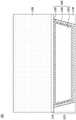
图1A示出了根据一些实施例的集成电路的半导体衬底和互连结构的截面图。1A illustrates a cross-sectional view of a semiconductor substrate and interconnect structure of an integrated circuit in accordance with some embodiments.
图1B示出了根据一些实施例的中间制造阶段的互连结构的透视图。FIG. 1B shows a perspective view of an interconnect structure at an intermediate stage of fabrication, according to some embodiments.
图2A至图10B示出了根据一些实施例的中间制造阶段的互连结构的截面图。2A-10B illustrate cross-sectional views of interconnect structures at intermediate stages of fabrication, according to some embodiments.
图11A、图11B和图11C示出了根据一些实施例的集成电路的半导体衬底和互连结构的截面图。11A, 11B, and 11C illustrate cross-sectional views of semiconductor substrates and interconnect structures of integrated circuits in accordance with some embodiments.
图12示出了根据一些实施例的中间制造阶段的互连结构的截面图。12 illustrates a cross-sectional view of an interconnect structure at an intermediate stage of fabrication, in accordance with some embodiments.
具体实施方式Detailed ways
下面的公开内容提供了用于实现本发明的不同特征的许多不同的实施例或示例。下文描述了组件和布置的具体示例以简化本公开。当然,这些仅是示例而不意图是限制性的。例如,在下面的说明中,在第二特征上方或之上形成第一特征可以包括以直接接触的方式形成第一特征和第二特征的实施例,并且还可包括可以在第一特征和第二特征之间形成附加特征,使得第一特征和第二特征可以不直接接触的实施例。此外,本公开可以在各个示例中重复参考数字和/或字母。该重复是出于简单和清楚的目的,并且其本身并不指示所讨论的各种实施例和/或配置之间的关系。The following disclosure provides many different embodiments or examples for implementing different features of the invention. Specific examples of components and arrangements are described below to simplify the present disclosure. Of course, these are only examples and are not intended to be limiting. For example, in the following description, forming a first feature on or over a second feature may include embodiments in which the first feature and the second feature are formed in direct contact, and may also include embodiments that may form the first feature and the second feature in direct contact. An embodiment in which an additional feature is formed between the two features so that the first feature and the second feature may not be in direct contact. Furthermore, the present disclosure may repeat reference numerals and/or letters in various examples. This repetition is for simplicity and clarity, and does not in itself indicate a relationship between the various embodiments and/or configurations discussed.
此外,本文中可能使用了空间相关术语(例如,“下方”、“之下”、“低于”、“以上”、“上部”等),以易于描述图中所示的一个要素或特征相对于另外(一个或多个)要素或(一个或多个)特征的关系。这些空间相关术语意在涵盖器件在使用或工作中除了图中所示朝向之外的不同朝向。装置可能以其他方式定向(旋转90度或处于其他朝向),并且本文中所用的空间相关描述符同样可被相应地解释。In addition, spatially relative terms (eg, "below," "below," "below," "above," "above," etc. may be used herein to facilitate the description of the relative relationship between an element or feature shown in a figure relationship to another element(s) or feature(s). These spatially relative terms are intended to encompass different orientations of the device in use or operation in addition to the orientation shown in the figures. The device may be otherwise oriented (rotated 90 degrees or at other orientations) and the spatially relative descriptors used herein interpreted accordingly.
本公开例如包括具有导电特征的互连结构的实施例,这些导电特征具有阻挡层、多个衬里层、以及导电填充材料。阻挡层被形成为未覆盖导电特征的底表面,这减小了器件电阻。处理工艺钝化了未被阻挡层覆盖的暴露底表面,这减少了可能由于随后形成的衬里层与暴露底表面之间的反应而产生的腐蚀。该多个衬里层可以在导电特征的侧壁上混合,这可以改善导电填充材料的粘附性。The present disclosure includes, for example, embodiments of interconnect structures having conductive features having barrier layers, multiple liner layers, and conductive fill materials. The barrier layer is formed not to cover the bottom surface of the conductive features, which reduces device resistance. The treatment process passivates the exposed bottom surface that is not covered by the barrier layer, which reduces corrosion that may occur due to reactions between a subsequently formed liner layer and the exposed bottom surface. The multiple liner layers can be mixed on the sidewalls of the conductive features, which can improve the adhesion of the conductive fill material.
图1A示出了根据一些实施例的半导体结构100的截面图,该半导体结构100包括可在其中形成各种电子器件的衬底50,以及形成在衬底50之上的多层互连系统(例如,互连层102)的一部分。图1B示出了如图1A所示的区域101的详细透视图。通常,如下面将更详细讨论的,图1A示出了形成在衬底50上的FinFET器件60,在其上形成有多个互连层。1A illustrates a cross-sectional view of a
通常,图1A所示的衬底50可包括体半导体衬底或绝缘体上硅(SOI)衬底。SOI衬底包括在薄半导体层下方的绝缘体层,该薄半导体层是SOI衬底的有效层。该有效层的半导体和体半导体通常包括晶体半导体材料硅,但可以包括一种或多种其他半导体材料,例如,锗、硅锗合金、化合物半导体(例如,GaAs、AlAs、InAs、GaN、AlN等)、或它们的合金(例如,GaxAl1-xAs、GaxAl1-xN、InxGa1-xAs等)、氧化物半导体(例如,ZnO、SnO2、TiO2、Ga2O3等)、或其组合。半导体材料可以被掺杂或不被掺杂。可以使用的其他衬底包括多层衬底、梯度衬底、或混合定向衬底。Generally, the
图1A所示的FinFET器件60是在半导体突起58的鳍状条带(称为鳍)中形成的三维MOSFET结构。图1A所示的截面是在与源极和漏极区域54之间的电流流动方向平行的方向上沿着鳍的纵轴截取的。鳍58可以通过使用光刻和蚀刻技术对衬底进行图案化来形成。例如,可以使用间隔件图像转印(SIT)图案化技术。在该方法中,使用合适的光刻和蚀刻工艺在衬底之上形成牺牲层并对其进行图案化以形成芯轴。使用自对准工艺在芯轴旁边形成间隔件。然后通过适当的选择性蚀刻工艺去除牺牲层。然后,每个剩余的间隔件可被用作硬掩模,以通过使用例如反应离子蚀刻(RIE)在衬底50中蚀刻沟槽来图案化各个鳍58。图1A示出了单个鳍58,但衬底50可以包括任何数量的鳍。The
图1A示出了沿着鳍58的相反侧壁形成的浅沟槽隔离(STI)区域62。STI区域62可如下形成:沉积一种或多种电介质材料(例如,氧化硅)以完全填充鳍周围的沟槽,然后使电介质材料的顶表面凹陷。STI区域62的电介质材料可以使用高密度等离子体化学气相沉积(HDP-CVD)、低压CVD(LPCVD)、低于大气压的CVD(SACVD)、可流动CVD(FCVD)、旋涂等、或其组合来沉积。在沉积之后,可以执行退火工艺或固化工艺。在一些情况下,STI区域62可以包括衬里(未示出),例如,通过氧化硅表面而生长的热氧化物衬里。凹陷工艺可以使用例如平坦化工艺(例如,化学机械抛光(CMP)),随后是选择性蚀刻工艺(例如,湿法蚀刻或干法蚀刻、或其组合),该选择性蚀刻工艺可以使STI区域62中的电介质材料的顶表面凹陷,使得鳍58的上部从周围的绝缘STI区域62突出。在一些情况下,还可以通过该平坦化工艺来去除用于形成鳍58的图案化硬掩模。FIG. 1A shows shallow trench isolation (STI)
在一些实施例中,图1A所示的FinFET器件60的栅极结构68是可以使用后栅极工艺流程形成的高k金属栅极(HKMG)栅极结构。在后栅极工艺流程中,在形成STI区域62之后形成牺牲虚设栅极结构(未示出)。虚设栅极结构可以包括虚设栅极电介质、虚设栅极电极和硬掩模。首先,可以沉积虚设栅极电介质材料(例如,氧化硅、氮化硅等)。接下来,可以在虚设栅极电介质之上沉积虚设栅极材料(例如,非晶硅、多晶硅等),然后将其平坦化(例如,通过CMP)。可以在虚设栅极材料之上形成硬掩模层(例如,氮化硅、碳化硅等)。然后,如下形成虚设栅极结构:使用适当的光刻和蚀刻技术对硬掩模进行图案化,并将该图案转移到虚设栅极电介质和虚设栅极材料。虚设栅极结构可以沿着突出的鳍的多个侧延伸,并且在鳍之间在STI区域62的表面之上延伸。如下面更详细地描述的,虚设栅极结构可被高k金属栅极(HKMG)栅极结构68代替,如图1A所示。图1A的右侧所示的HKMG栅极结构68(在鳍58的顶部可见)是有效HKMG栅极结构的示例,其例如沿着鳍58的突出高于STI区域62的一部分的侧壁并在该部分之上延伸,以及图1A左侧的HKMG栅极结构68是在STI区域62之上(例如,在相邻的鳍之间)延伸的示例栅极结构。用于形成虚设栅极结构和硬掩模的材料可以使用任何合适的方法(例如,CVD、等离子体增强CVD(PECVD)、原子层沉积(ALD)、等离子体增强ALD(PEALD)等)来沉积、或通过半导体表面的热氧化来沉积、或其组合。In some embodiments,
图1A所示的FinFET 60的源极和漏极区域54和间隔件72被形成为例如与虚设栅极结构自对准。可以通过在虚设栅极图案化完成之后执行的间隔件电介质层的沉积和各向异性蚀刻来形成间隔件72。间隔件电介质层可以包括一种或多种电介质,例如,氧化硅、氮化硅、氮氧化硅、碳化硅、碳氮化硅等、或其组合。该各向异性蚀刻工艺从虚设栅极结构的顶部之上去除电介质间隔件层,从而使沿着虚设栅极结构的侧壁的间隔件72横向延伸到鳍的表面的一部分上(如图1A右侧所示)或STI电介质的表面上(如图1A左侧所示)。The source and drain
源极和漏极区域54是与半导体鳍58接触的半导体区域。在一些实施例中,源极和漏极区域54可以包括重掺杂区域和相对轻掺杂的漏极延伸部或LDD区域。通常,重掺杂区域使用间隔件72而与虚设栅极结构间隔开,而LDD区域可以在形成间隔件72之前形成,并因此在间隔件72下方延伸,并且在一些实施例中,进一步延伸至半导体在虚设栅极结构下方的一部分中。LDD区域可以例如通过使用离子注入工艺注入掺杂剂(例如,As、P、B、In等)来形成。Source and
源极和漏极区域54可以包括外延生长区域。例如,在形成LDD区域之后,可以形成间隔件72,随后,重掺杂源极和漏极区域可如下形成为与间隔件72自对准:首先蚀刻鳍以形成凹部,然后通过选择性外延生长(SEG)工艺在凹部中沉积晶体半导体材料,其填充凹部并通常延伸到鳍的原始表面之外而形成凸起源极-漏极结构,如图1A所示。晶体半导体材料可以是元素的(例如,Si或Ge等)或合金的(例如,Si1-xCx或Si1-xGex等)。SEG工艺可以使用任何合适的外延生长方法,例如,气相/固相/液相外延(VPE、SPE、LPE)、或金属有机CVD(MOCVD)、或分子束外延(MBE)等。高剂量(例如,约1014cm-2至1016cm-2)的掺杂剂可以在SEG期间被原位引入到重掺杂源极和漏极区域54中、或通过在SEG之后执行的离子注入工艺引入、或其组合。Source and
层间电介质(ILD)层76(在图1A中可见)被沉积在结构之上。在一些实施例中,可以在沉积ILD材料之前沉积合适的电介质(例如,氮化硅、碳化硅等、或其组合)的接触蚀刻停止层(CESL)(未示出)。可以执行平坦化工艺(例如,CMP)来从虚设栅极之上去除过量的ILD材料和任何剩余的硬掩模材料以形成顶表面,其中,虚设栅极材料的顶表面被暴露并且可以与ILD层76的顶表面基本上共面。图1A所示的HKMG栅极结构68可然后如下形成:首先使用一个或多个蚀刻技术去除虚设栅极结构,从而在相应的间隔件72之间形成凹部。An interlayer dielectric (ILD) layer 76 (visible in FIG. 1A ) is deposited over the structure. In some embodiments, a contact etch stop layer (CESL) (not shown) of a suitable dielectric (eg, silicon nitride, silicon carbide, etc., or combinations thereof) may be deposited prior to depositing the ILD material. A planarization process (eg, CMP) may be performed to remove excess ILD material and any remaining hard mask material from over the dummy gate to form a top surface, wherein the top surface of the dummy gate material is exposed and can be interacted with the ILD. The top surfaces of
接下来,沉积包括一种或多种电介质的替换栅极电介质层66,随后沉积包括一种或多种导电材料的替换导电栅极层64,以完全填充凹部。栅极电介质层66包括例如高k电介质材料,例如,金属的氧化物和/或硅酸盐(例如,Hf、Al、Zr、La、Mg、Ba、Ti、以及其他金属的氧化物和/或硅酸盐)、氮化硅、氧化硅等、或其组合、或其多层。在一些实施例中,导电栅极层64可以是多层金属栅极堆叠,其包括相继形成在栅极电介质层66的顶部上的阻挡层、功函数层和栅极填充层。阻挡层的示例材料包括TiN、TaN,Ti、Ta等、或其多层组合。对于p型FET,功函数层可以包括TiN、TaN、Ru、Mo、Al,并且对于n型FET,功函数层可以包括Ti、Ag、TaAl、TaAlC、TiAlN、TaC、TaCN、TaSiN、Mn、Zr。可以使用其他合适的功函数材料、或其组合、或其多层。填充凹部的其余部分的栅极填充层可以包括诸如Cu、Al、W、Co、Ru等之类的金属、或其组合、或其多层。可以通过任何合适的方法来沉积用于形成栅极结构的材料,例如,CVD、PECVD、PVD、ALD、PEALD、电化学镀(ECP)、化学镀等。可以使用例如CMP工艺来从ILD层76的顶表面之上去除栅极结构层64和66的多余部分。如图1A所示的所得结构可以是基本上共面的表面,包括下列项的的暴露顶表面:ILD层76、间隔件72、以及嵌入在相应的间隔件72之间的HKMG栅极层66和64的其余部分。Next, a replacement
如图1A所示,可以在ILD层76之上沉积ILD层78。在一些实施例中,用于形成ILD层76和ILD层78的绝缘材料可以包括氧化硅、磷硅酸盐玻璃(PSG)、硼硅酸盐玻璃(BSG)、掺杂硼的磷硅酸盐玻璃(BPSG)、未掺杂的硅酸盐玻璃(USG)、多孔或致密的低介电常数(低k)电介质,例如,氟硅酸盐玻璃(FSG)、碳氧化硅(SiOCH)、掺杂碳的氧化物(CDO)、可流动氧化物、或多孔氧化物(例如,干凝胶/气凝胶)等、或其组合。可以使用任何合适的方法来沉积用于形成ILD层76和ILD层78的电介质材料,例如,CVD、物理气相沉积(PVD)、ALD、PEALD、PECVD、SACVD、FCVD、旋涂等、或其组合。As shown in FIG. 1A , an
如图1A所示,在衬底50中形成的电子器件的电极可以使用在电介质层中形成的导电连接器(例如,接触件74)而电连接至互连层102的导电特征。在图1A所示的示例中,接触件74电连接到FinFET 60的源极和漏极区域54。对于栅极电极的接触件74通常形成在STI区域62之上。单独的栅极电极64(在图1A的左侧示出)示出了这种接触件。可以使用光刻技术来形成接触件。例如,图案化掩模可形成在ILD层78之上并用于蚀刻开口,这些开口延伸穿过ILD层78而暴露栅极电极在STI区域62之上的一部分,以及在鳍58之上蚀刻开口,这些开口进一步延伸穿过ILD层76以及ILD层76下方的CESL(未示出)衬里而暴露源极和漏极区域54的一些部分。在一些实施例中,可使用各向异性干法刻蚀工艺,其中,该刻蚀在两个连续步骤中执行。相对于在栅极电极64和CESL中使用的材料的蚀刻速率,用于该蚀刻工艺的第一步骤的蚀刻剂对ILD层76和78的材料具有更高的蚀刻速率,其可以内衬(lining)源极和漏极区域54的重掺杂区域的顶表面。一旦该蚀刻工艺的第一步骤暴露CESL,就可以执行该蚀刻工艺的第二步骤,其中,可以切换蚀刻剂以选择性地去除CESL。As shown in FIG. 1A , electrodes of electronic devices formed in
在一些实施例中,可以在ILD层76和ILD层78中的开口中形成导电衬里。随后,用导电填充材料填充开口。衬里包括阻挡金属,这些阻挡金属用于减少导电材料从接触件74向外扩散到周围的电介质材料中。在一些实施例中,衬里可包括两个阻挡金属层。第一阻挡金属层与源极和漏极区域54中的半导体材料接触,并且随后可以与源极和漏极区域54中的重掺杂半导体进行化学反应而形成低电阻欧姆接触件,此后,未反应的金属可被去除。例如,如果源极和漏极区域54中的重掺杂半导体是硅或硅锗合金半导体,则第一阻挡金属层可以包括Ti、Ni、Pt、Co、其他合适的金属、或其合金。导电衬里的第二阻挡金属层可以另外包括其他金属(例如,TiN、TaN、Ta、或其他合适的金属、或其合金)。可以使用任何可接受的沉积技术(例如CVD、ALD、PEALD、PECVD、PVD、ECP、化学镀等、或其任何组合)来将导电填充材料(例如,W、Al、Cu、Ru、Ni、Co、其合金、其组合等)沉积在导电衬里之上,以填充接触开口。接下来,可以使用平坦化工艺(例如,CMP)来从ILD层78的表面之上去除导电材料的多余部分。所得的导电插塞延伸到ILD层76和78中,并且构成实体连接并电连接到电子器件(例如,图1A所示的三栅极FinFET 60)的电极的接触件74。在该示例中,使用相同的处理步骤同时形成对于STI区域62之上的电极以及对于鳍58之上的电极的接触件。然而,在其他实施例中,这两种类型的接触件可单独地形成。In some embodiments, conductive liners may be formed in the openings in
在一些实施例中,穿过ILD层76和78至STI区域62或衬底50的顶表面形成导电插塞75。导电插塞75形成密封环80的底部,密封环80可以包括位于半导体结构100的每个后续形成的层上的互连金属部件。密封环80可以是在集成电路周围形成的应力保护结构,并且可以保护半导体芯片的内部电路(例如,包括FinFET 60的电路)免受湿气或免受由于诸如从晶圆分离半导体芯片之类的工艺而引起的损坏。导电插塞75可以使用与上述接触件74类似的方法和材料来形成。然而,可以使用任何合适的方法和材料来形成导电插塞75。In some embodiments,
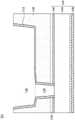
图1B图示了图1A的区域101的详细透视图,示出了互连层102的顶部。如图1A和图1B所示,根据一些实施例,根据集成电路设计所采用的后端线(BEOL)方案,互连层102被形成、堆叠在形成于ILD层76和78中的接触件74的垂直上方。在图1A所示的BEOL方案中,各个互连层具有类似的特征。然而,应理解,其他实施例可以采用替代的集成方案,其中各个互连层可以使用不同的特征。例如,被示为垂直连接器的接触件74可被延伸以形成横向传输电流的导电线,并且导电插塞75也可被延伸以形成作为密封环80的部分的导电线。FIG. 1B illustrates a detailed perspective view of
互连层(例如,互连层102)包括嵌入在金属间电介质(IMD)层中的导电过孔和导电线。除了在各种导电元件之间提供绝缘之外,IMD层还可包括一个或多个电介质蚀刻停止层以控制在IMD层中形成开口的蚀刻工艺。通常,过孔垂直地传导电流并用于电连接位于垂直相邻的层的两个导电特征,而线横向地传导电流并用于在一个层内分配电信号和功率。在根据图1A和图1B示出的实施例中,导电线105将接触件74连接至随后形成的导电过孔,并且在后续层处,过孔将位于过孔下方的层的线连接至过孔上方的线(例如,一对线可由过孔连接)。其他实施例可以采用不同的方案。例如,导电过孔可以在接触件74和导电线105之间的互连层102中。The interconnect layer (eg, interconnect layer 102 ) includes conductive vias and conductive lines embedded in an intermetal dielectric (IMD) layer. In addition to providing isolation between the various conductive elements, the IMD layer may include one or more dielectric etch stop layers to control the etching process that forms the openings in the IMD layer. Typically, vias conduct current vertically and are used to electrically connect two conductive features located in vertically adjacent layers, while wires conduct current laterally and are used to distribute electrical signals and power within a layer. In the embodiment shown according to FIGS. 1A and 1B , the
仍参考图1A和图1B,互连层102可以使用例如镶嵌工艺流程来形成。首先,可以使用在ILD层76和78的描述中列出的一层或多层电介质材料来沉积用于形成IMD层110的电介质堆叠。在一些实施例中,IMD层110包括位于电介质堆叠的底部的蚀刻停止层(未示出)。蚀刻停止层包括具有与上面的材料的蚀刻速率不同的蚀刻速率的一个或多个绝缘体层(例如,SiOx、SiOC、SiCN、SiOxNy、SiN、CN、AlOx、AlN、AlYOx、ZrOx、YOx、其组合等)。用于沉积用于IMD的电介质堆叠的技术可以与用于形成ILD层76和78的技术相同。Still referring to FIGS. 1A and 1B , the
可以使用适当的光刻和蚀刻技术(例如,采用碳氟化合物的各向异性RIE)来图案化IMD层110以形成用于线的开口。用于线的开口可以是在IMD层110中形成的纵向沟槽。蚀刻技术可以采用多个步骤。例如,第一主蚀刻步骤可以去除IMD层110的电介质材料的一部分,并且在蚀刻停止电介质层上停止。然后,可以切换蚀刻剂以去除蚀刻停止层电介质材料。可以调节各个蚀刻步骤的参数(例如,气体的化学成分、流速和压力、反应器功率等)以产生具有期望的内部锥角的渐缩侧壁轮廓。The
可以沉积若干导电材料以填充沟槽,形成互连层102的导电线105。开口可被首先内衬一个或多个衬里,然后填充导电填充层104,其可以被帽盖层覆盖。Several conductive materials may be deposited to fill the trenches, forming
可以在沟槽的侧壁和底表面之上形成导电扩散阻挡衬里。导电扩散阻挡衬里可以包括一层或多层TaN、Ta、TiN、Ti、Co等、或其组合,例如,外部衬里108和下部内部衬里106A。导电扩散阻挡衬里可以通过任何合适的方法来沉积,例如,CVD、PECVD、PVD、ALD、PEALD、电化学镀(ECP)、化学镀等。在一些实施例中,外部衬里108包括TaN,并且下部内部衬里106A包括Co。A conductive diffusion barrier liner may be formed over the sidewalls and bottom surface of the trench. The conductive diffusion barrier liner may include one or more layers of TaN, Ta, TiN, Ti, Co, etc., or a combination thereof, eg, the
接下来,在导电扩散阻挡衬里之上形成导电填充层104以填充沟槽,形成导电线105。导电填充层104可以包括诸如W、Cu、Co、Ru、CuMn、Mo、Al等之类的金属、或其组合、或其多层。在一些实施例中,导电填充层104是铜。可以通过任何合适的方法来沉积用于形成导电填充层104的导电材料,例如,CVD、PECVD、PVD、ALD、PEALD、电化学镀(ECP)、化学镀等。在一些实施例中,可以在导电扩散阻挡衬里之上沉积薄的导电种子层以辅助发起ECP沉积步骤,该ECP沉积步骤用导电填充材料来完全填充开口。导电种子层可以是与导电填充层相同的导电材料,并且可以使用适当的沉积技术(例如,CVD、PECVD、ALD、PEALD或PVD等)来沉积。Next, a
在形成导电填充层104之后,可以在导电填充层104之上形成帽盖层106B。在沉积用于帽盖层106B的材料之后,可利用任何合适的方法(例如,使用光刻)来去除多余部分。这样,可以在帽盖层106B的材料之上形成光致抗蚀剂(未具体示出),并对其进行图案化以暴露帽盖层106B的材料的不在导电填充层104和下部内部衬里106A正上方的部分。这些暴露的部分然后可以通过蚀刻或任何合适的方法来去除。在一些实施例中,帽盖层106B是使用诸如ALD工艺之类的选择性沉积工艺来形成的,该选择性沉积工艺将帽盖层106B沉积在导电填充层104、外部衬里108和下部内部衬里106A的金属表面上,但未显著地沉积在IMD层110的电介质表面上。在一些实施例中,帽盖层106B是与下部内部衬里106A相同的材料,并且下部内部衬里106A和帽盖层106B一起形成同一材料(例如,Co)的内部衬里106。After the
可以在导电插塞75之上形成导电线107来作为密封环80的部分。导电线107可以使用与导电线105类似的材料和方法来形成。在一些实施例中,导电线107形成有比导电线105更大的宽度。
可以通过平坦化工艺(例如,CMP)来去除IMD层110之上的和/或外部衬里108的顶表面上的在开口外部的任何多余的导电材料,从而形成这样的顶表面,该顶表面包括与线105的导电区域基本上共面的IMD层110的电介质区域。该平坦化步骤完成了包括嵌入在IMD层110中的导电线105和107的互连层102的制造,如图1A和图1B所示。Any excess conductive material outside the openings over the
图1B进一步示出了在后面的图中使用的参考截面。截面A-A’沿着导电线105的纵轴,并且截面B-B’垂直于截面A-A’。FIG. 1B further shows the reference section used in subsequent figures. Section A-A' is along the longitudinal axis of
图2A至图10B是根据一些实施例的制造互连结构的中间阶段的截面图和透视图。图2A、图3A、图4A、图4C、图5A、图6B、图7A和图8A沿图1B所示的截面A-A’示出。图2B、图3B、图4B、图4D、图5B、图6A、图6C、图6D、图7B、图7C、图8B、图9A、图9B、图10A和图10B沿图1B所示的截面B-B’示出。2A-10B are cross-sectional and perspective views of intermediate stages of fabricating an interconnect structure in accordance with some embodiments. Figures 2A, 3A, 4A, 4C, 5A, 6B, 7A and 8A are shown along section A-A' shown in Figure IB. Figure 2B, Figure 3B, Figure 4B, Figure 4D, Figure 5B, Figure 6A, Figure 6C, Figure 6D, Figure 7B, Figure 7C, Figure 8B, Figure 9A, Figure 9B, Figure 10A, and Figure 10B Section BB' is shown.
图2A和图2B示出了形成包括位于互连层102之上的蚀刻停止层(ESL)116和电介质层120的电介质堆叠。该电介质堆叠可用于在形成于互连层102上的互连层140中后续形成导电通孔和导电线(参见下面的图8A和图8B)。ESL 116被形成在互连层102上。ESL 116可用于控制后续蚀刻工艺以形成用于过孔的开口(参见下面的图3A和图3B)。ESL 116包括具有与下面的IMD 110以及后续形成的上面的材料的蚀刻速率不同的蚀刻速率的一个或多个绝缘体层,例如,SiN、SiC、AlOx、AlN、AlYOx、ZrOx、YOx、其组合等。ESL 116可以使用PECVD、ALD、CVD等来形成。2A and 2B illustrate the formation of a dielectric stack including an etch stop layer (ESL) 116 and a
接下来,在ESL 116上形成电介质层120。电介质层120包括一个或多个绝缘体层,例如,SiOx、SiOC、SiCN、SiOxNy、SiN等。根据一些实施例,电介质层120使用PECVD、FCVD、旋涂等来形成。Next, a
在图3A和图3B中,利用适当的光刻和蚀刻技术(例如,采用碳氟化合物的各向异性RIE)来在电介质层120中形成用于过孔的开口124和用于线的开口126。用于过孔的开口124可以是延伸穿过电介质层120和ESL116而暴露导电线105的顶部导电表面的垂直孔,并且用于线的开口126可以是形成在电介质层120的上部中的纵向沟槽。在一些实施例中,用于在电介质层120中图案化孔和沟槽的方法利用过孔优先(via-first)方案,其中,第一光刻和蚀刻工艺形成用于过孔的孔,并且第二光刻和蚀刻工艺形成用于线的沟槽。其他实施例可以使用不同的方法,例如,沟槽优先方案、或不完全的过孔优先方案、或掩埋蚀刻停止层方案。这些蚀刻技术可以采用多个步骤。例如,第一主蚀刻步骤可以去除电介质层120的电介质材料的一部分,并在ESL 116上停止。然后,可以切换蚀刻剂以去除ESL 116的电介质材料。可以调节各个蚀刻步骤的参数(例如,气体的化学成分、流速和压力、反应器功率等)以产生具有期望的内部锥角的渐缩侧壁轮廓。在其中导电线105的内部衬里106的顶部覆盖导电填充层104的顶表面的一些实施例中,开口124可延伸穿过内部衬里106的顶部而暴露导电填充层104的顶表面。In FIGS. 3A and 3B ,
在图4A和图4B中,在开口124的侧壁上以及在开口126的侧壁和底表面上执行阻挡层132的选择性沉积。阻挡层132可以减少原子从随后沉积的导电材料(参见下面的图6A和图6B)到电介质层120的扩散。在一些实施例中,阻挡层132的选择性沉积减少了沉积在开口124的底表面上的阻挡材料的量,使得很少或没有阻挡层132被形成在导电填充层104上。这可以减小导电填充层104与随后沉积的外部衬里134(参见下面的图6A和图6B)之间的电阻。In FIGS. 4A and 4B , selective deposition of
作为阻挡层132的选择性沉积的示例,可以在导电填充层104的暴露部分上形成牺牲层(未示出),以阻挡、防止、或以其他方式抑制阻挡层132后续形成在导电填充层104上。牺牲层可被沉积为使得很少或没有牺牲层的材料被形成在ESL 116或电介质层120上。牺牲层包括粘附或键合至导电填充层104,并且不粘附或键合至电介质层120和/或ESL 116的材料。例如,该材料可以与导电填充层104的金属(例如,铜)形成螯合键,但不与电介质层120或ESL 116形成键。在一些实施例中,牺牲层包括有机分子,例如,苯并三唑(BTA),化学式为C6H4N3H。BTA分子具有带有三个氮原子(可键合至诸如铜之类的金属)的第一侧以及具有疏水性苯并环的第二侧,阻挡层132的一些前体不能键合至该疏水性苯并环。BTA分子的第一侧可以键合到导电填充层104,而第二侧突出并阻止前体键合到导电填充层104。以这种方式,包括BTA单层或多个BTA单层的牺牲层可以防止阻挡层132形成在导电填充层104上或牺牲层上。As an example of selective deposition of
在形成牺牲层之后,在开口124的侧壁上以及在开口126的侧壁和底表面上形成阻挡层132。阻挡层132可以包括阻挡材料,例如,钽、氮化钽、钛、氮化钛等、或其组合。阻挡层132可以使用诸如ALD工艺和/或CVD工艺之类的合适的工艺来形成。阻挡层132被形成在电介质层120和ESL 116的暴露表面之上,但是被牺牲层阻止形成在开口124内的导电填充层104上。此外,如前所述,阻挡层132未显著地形成在牺牲层的暴露表面上。在形成阻挡层132之后,可以通过诸如热处理或等离子体处理(例如,原位H2或Ar等离子体处理)之类的合适的工艺来去除牺牲层。电介质层120之上的阻挡层132的多余部分可以利用诸如CMP之类的平坦化来去除。After the sacrificial layers are formed, barrier layers 132 are formed on the sidewalls of
在一些实施例中,阻挡层132在开口124的侧壁上以及在开口126的侧壁和底表面上被形成为


图4C和图4D示出了其中在开口124的底表面上形成底部阻挡层132A的实施例。可以在开口124的侧壁上以及在开口126的侧壁和底表面上形成阻挡层132期间形成底部阻挡层132A。底部阻挡层132A可以是不连续的,并且可以覆盖开口124的底表面的10%至90%的范围内的百分比。底部阻挡层132A的厚度可以在


在图5A和图5B中,分别在图4A和图4B之后,对通过开口124暴露的导电填充层104的顶表面执行处理工艺150。处理工艺150可以利用随后形成的外部衬里134(参见下面的图6A和图6B)来钝化导电填充层104的暴露的下面的表面,这可以减少可由反应(例如,氧化还原反应)引起的导电填充层104的顶表面的腐蚀。在一些实施例中,随后形成的外部衬里134包括钌(Ru),其具有比Cu和Co更高的还原电势。因此,随后形成的包括Ru的外部衬里134实体接触包括例如Cu或Co的导电填充层104可能提高触发氧化还原反应的可能性,这些氧化还原反应可能腐蚀导电填充层104的顶表面并降低器件性能。处理工艺150可以通过钝化导电填充层104来降低导电填充层104的顶表面的腐蚀的可能性。In FIGS. 5A and 5B , after FIGS. 4A and 4B , respectively, a treatment process 150 is performed on the top surface of the
处理工艺150可以是对导电填充层104的暴露表面(可以是例如铜或钴)的清洁处理,例如,等离子体或轰击处理。处理工艺150可以降低导电填充层104的暴露表面上的杂质水平,例如,C、N、O和F杂质。在一些实施例中,该处理工艺是使用H2、Ar、N2、NH3、O2等、或其组合的等离子体处理。该等离子体处理可以以在电源处测量的100W至800W的范围内的功率执行,这可以减少杂质以及随后对导电填充层104的顶表面的腐蚀。以小于100W执行该等离子体处理可能是不利的,因为会导致杂质的去除不充分以及对导电填充层104的顶表面的腐蚀增加。以大于800W执行该等离子体处理可能是不利的,因为会导致对导电填充层104的顶表面的损坏。该等离子体处理可被执行10秒至2分钟的范围内的持续时间,这可以减少杂质以及随后对导电填充层104的顶表面的腐蚀。执行该等离子体处理少于10秒可能是不利的,因为会导致杂质的去除不充分以及对导电填充层104的顶表面的腐蚀增加。执行该等离子体处理多于2分钟可能是不利的,因为会导致对导电填充层104的顶表面的损坏。The treatment process 150 may be a cleaning process, such as a plasma or bombardment process, of the exposed surface of the conductive fill layer 104 (which may be, for example, copper or cobalt). The treatment process 150 may reduce impurity levels, eg, C, N, O, and F impurities, on the exposed surface of the
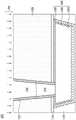
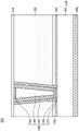
在图6A至图6D中,穿过电介质层120形成导电特征130和170。图6A示出了包括互连层102和140的半导体结构100的截面图。图6B和图6C分别沿着截面A-A’和B-B’示出了图6A所示的区域101的截面图。图6D沿着截面B-B’示出了图6A所示的区域201的截面图。导电特征130可以包括填充开口124的过孔部分以及填充开口126的线部分,并且导电特征170可以使用与导电特征130类似的方法和材料来形成,但具有比导电特征130更宽的尺寸。在一些实施例中,导电特征130和170包括外部衬里134、内部衬里136和导电填充材料138。In FIGS. 6A-6D ,
外部衬里134在开口124和126中被形成在阻挡层132和导电填充层104的暴露表面之上。外部衬里134可以由钌、钼、铑等形成,并且可以通过诸如CVD、PVD、ALD等、或其组合之类的沉积工艺来形成。根据一些实施例,外部衬里134可以通过流动前体分子来利用CVD工艺形成,该前体分子包含连接到一个或多个烷基(例如,己二烯、吡啶、丁二烯和环庚二烯)、一个或多个羰基、一个或多个其他官能团、或其组合的钌(Ru)。例如,可以使用三羰基-己二烯钌作为前体分子来通过CVD形成外部衬里134。用钌形成外部衬里134的益处是铜对钌的粘附性弱于阻挡层132(例如,TaN)对铜的粘附性,这可以改善导电填充层138(例如,铜)的填充工艺,因为铜更容易在钌基表面上流动。电介质层120之上的外部衬里134的多余部分可以用诸如CMP之类的平坦化来去除。
在一些实施例中,外部衬里134在开口124的侧壁和底表面上以及在开口126的侧壁和底表面上被共形地形成为


在形成外部衬里134之后,可以形成内部衬里136和导电填充层138以填充开口124和126。内部衬里136可以改善外部衬里134和导电填充层138之间的粘附性。内部衬里136和导电填充层138可以分别使用与内部衬里106和导电填充层104类似的材料和方法来形成,如以上关于图1A和图1B所述。例如,可以首先使用与下部内部衬里106A(参见上面的图1B)类似的方法和材料来形成内部衬里136的下部内部衬里部分。可以在内部衬里136的下部内部衬里部分之上形成导电填充层138,然后使用与帽盖层106B(参见上面的图1B)类似的方法和材料在导电填充层138之上形成内部衬里136的帽盖部分,使得内部衬里136覆盖导电填充层138的底表面、侧壁和顶表面。在一些实施例中,内部衬里136包括钴,导电填充层138包括铜,并且内部衬里136的钴可以改善导电填充层138的铜对外部衬里134的钌的后续粘附性。After
在一些实施例中,内部衬里136被形成为


图6D示出了可以形成在导电线107之上来作为密封环80(参见上面的图1A)的部分的导电特征170。导电特征170可以使用与导电特征130类似的材料和方法来形成。在一些实施例中,导电特征170被形成为具有比导电特征130更大的宽度。例如,导电特征130可具有跨导电特征130的底表面测量的宽度W1,该宽度W1在10nm至22nm的范围内,并且导电特征170可具有跨导电特征170的底表面测量的宽度W2,该宽度W2在100nm至180nm的范围内。导电特征170的底表面可以与导电线107的顶表面的外边缘分开最大间隔长度L1和最小间隔长度L2,其中,最大间隔长度L1和最小间隔长度L2之间的差在0.5nm至5nm的范围内。FIG. 6D shows
可以通过平坦化工艺(例如,CMP)来去除电介质层120之上的和/或外部衬里134的顶表面上的在开口124和126外部的任何多余的导电材料,从而形成这样的顶表面,该顶表面包括与导电特征130的导电区域基本上共面的电介质层120的电介质区域。该平坦化步骤完成了包括嵌入在电介质层120中的导电特征130和/或170的互连层140的制造。Any excess conductive material outside of
在图7A、图7B和图7C中,在互连层140之上形成ESL 142。ESL 142可用于控制后续蚀刻工艺以在随后形成在互连层140之上的互连层(参见下面的图12)中形成用于过孔的开口。ESL 142可以使用与以上关于图2A和图2B所述的ESL 116类似的方法和材料来形成。In FIGS. 7A , 7B and 7C ,
图8A和图8B示出了在图4C和图4D之后的实施例。导电特征130的底部阻挡层132A介于外部衬里134的底表面和导电填充层104的顶表面之间。底部阻挡层132A可以是不连续的,这可以减小外部衬里134和导电填充层104之间的电阻。Figures 8A and 8B illustrate the embodiment following Figures 4C and 4D.
图9A和图9B示出了一个实施例,其中,通过沿阻挡层132的侧壁的外部衬里134和内部衬里136的混合而在导电特征130和170中形成组合衬里135。在其中外部衬里134包括钌并且内部衬里136包括钴的实施例中,组合衬里135包括混合的钌和钴。具有混合的钌和钴的组合衬里135可以提高用导电填充层138填充开口124和126的效率和良率。具体地,在其中导电填充层138包括Cu的一些实施例中,在结合衬里135的表面上存在钌通过具有经提高的从结合衬里135的Cu去湿性(dewettability),而提供了改善的导电填充层138的沉积和回流。通过例如在能量色散X射线光谱扫描中具有重叠的强度峰值,沿着阻挡层132的侧壁的结合衬里135可被测量为具有完全混合的钌和钴。FIGS. 9A and 9B illustrate an embodiment in which a
在一些实施例中,组合衬里135是在形成外部衬里134和内部衬里136之后并且在形成导电填充层138之前,通过对半导体结构100执行诸如氢浸泡处理和/或氢等离子体处理之类的氢处理(参见上面的图6A)来形成的。在氢浸泡处理期间,氢气扩散到组合衬里135中以修复变形并重新定向分子,这促进了外部衬里134和内部衬里136之间的混合。氢浸泡处理可以在200℃至500℃的范围内的高温,以及10Torr至50Torr的范围内的高压下执行。氢等离子体处理也可以促进外部衬里134和内部衬里136之间的混合。此外,氢离子与外部衬里134和内部衬里136反应以从这些层中去除碳和氧杂质,同时还提高了金属扩散性。根据一些实施例,氢等离子体处理包括用氢等离子体轰击半导体结构100达10秒至120秒的范围内的时间段。氢等离子体处理可以在150℃至400℃的范围内的温度,以及1Torr至10Torr的范围内压力下执行。氢等离子体的流速可以在1000sccm(标准立方厘米每分钟)至6000sccm的范围内,并且持续10秒至2分钟的范围内的持续时间。In some embodiments, the combined
如图9A和图9B所示,可以在导电特征130和170中在阻挡层132的侧壁上形成组合衬里135。外部衬里134和内部衬里136的沿着导电特征130和170的底表面的部分可以被部分地混合,或者可以保持未混合。通过例如在能量色散X射线光谱扫描中具有部分重叠的强度峰值,外部衬里134和内部衬里136的沿着导电特征130和170的底表面的部分可被测量为具有部分地混合的钌和钴。在一些实施例中,组合衬里135在导电特征130和170的侧壁上的厚度在


图10A和图10B示出了一个实施例,其中,导电填充层138直接形成在导电特征130和170中的外部衬里134上。在开口124的侧壁和底表面上以及在开口126的侧壁和底表面上,外部衬里134可被形成为


图11A、图11B和图11C示出了其中互连层102和140被形成在不同的电子器件之上的实施例的剖视图。提供图1A和图6A所示的示例电子器件(FinFET 60)仅出于说明性目的,以进一步解释对所公开的实施例的应用,并不意味着以任何方式限制所公开的实施例。图11A示出了FinFET器件60’的另一配置,其中双鳍58’被栅极结构68覆盖。所公开的FinFET实施例还可应用于纳米结构器件,例如,纳米结构(例如,纳米片、纳米线、栅极全环绕等)场效应晶体管(nano-FET)。在纳米结构FET实施例中,鳍被纳米结构代替,纳米结构是通过对沟道层和牺牲层的交替层的堆叠进行图案化而形成的。以与上述实施例类似的方式形成虚设栅极堆叠和源极/漏极区域。在去除虚设栅极堆叠之后,可以在沟道区域中部分地或完全去除牺牲层。以与上述实施例类似的方式形成替换栅极结构,替换栅极结构可以部分地或完全填充由去除牺牲层而留下的开口,并且替换栅极结构可部分地或完全围绕纳米结构FET器件的沟道区域中的沟道层。图11B示出了纳米片沟道区域158被栅极结构68覆盖的纳米片器件160,以及图11C示出了纳米线沟道区域258被栅极结构68覆盖的纳米线器件260。可以以与上述实施例类似的方式形成ILD以及对替代栅极结构和源极/漏极区域的接触件。可以如美国专利申请公开号2016/0365414中所公开的来形成纳米结构器件,该专利申请通过引用整体并入本文。11A, 11B, and 11C illustrate cross-sectional views of embodiments in which interconnect layers 102 and 140 are formed over different electronic devices. The example electronic device (FinFET 60) shown in FIGS. 1A and 6A is provided for illustrative purposes only to further explain the application of the disclosed embodiments and is not meant to limit the disclosed embodiments in any way. FIG. 11A shows another configuration of FinFET device 60' in which dual fins 58' are covered by
图12示出了根据一些实施例的互连层140的截面图,其中更高的互连层240和340沿着图1B的截面B-B’形成在互连层140上。在根据图12示出的实施例中,各个互连层具有类似的特征并且可以使用类似的方法和材料来形成。互连层240和340的电介质层220和230可分别使用与电介质层120类似的方法和材料来形成,并且互连层240的导电特征230和270以及互连层340的导电特征330和370可使用与导电特征130和170类似的方法和材料来形成,如以上关于图2A至图6D所述。然而,应理解,其他实施例可采用其中各个互连层可使用不同特征的替代集成方案。例如,互连层140和340的导电特征130和330被分别示出为具有垂直于截面B-B’延伸的导电线部分,而互连层240的导电特征240被示出为具有沿着截面B-B’延伸的导电线部分。在其他实施例中,互连层140和340的导电特征130和330可具有沿着截面B-B’延伸的导电线部分,并且互连层240的导电特征230可具有垂直于截面B-B’延伸的导电线部分。尽管被示出为形成在同一截面中,但应理解,导电特征130、230和330中的每一个可形成在不同的截面中,这可以避免导电特征的短路。12 illustrates a cross-sectional view of
如图12所示的各个互连层的导电特征可具有不同的尺寸。例如,在一些实施例中,互连层140的导电特征130具有跨底表面测量的10nm至15nm范围内的宽度W3,互连层240的导电特征230具有跨底表面测量的14nm至22nm范围内的宽度W4,并且互连层340的导电特征330具有跨底表面测量的12nm至16nm范围内的宽度W5。The conductive features of the various interconnect layers as shown in FIG. 12 may have different dimensions. For example, in some embodiments,
实施例可以提供优点。互连结构可形成有导电特征,这些导电特征具有被形成为未覆盖导电特征的底表面的阻挡层,以降低器件电阻。未被阻挡层覆盖的暴露底表面可以被钝化,这可以减少由于随后形成的衬里层与暴露底表面之间的反应而引起的腐蚀。可以在阻挡层之上形成多个衬里层。该多个衬里层可以在导电特征的侧壁上混合,以改善随后形成以填充导电特征的导电填充材料的粘附性。Embodiments may provide advantages. The interconnect structure can be formed with conductive features with barrier layers formed to not cover the bottom surfaces of the conductive features to reduce device resistance. The exposed bottom surface not covered by the barrier layer can be passivated, which can reduce corrosion due to reactions between the subsequently formed liner layer and the exposed bottom surface. Multiple backing layers may be formed over the barrier layer. The plurality of liner layers may be mixed on the sidewalls of the conductive features to improve adhesion of the conductive fill material subsequently formed to fill the conductive features.
根据一个实施例,一种制造结构的方法包括:穿过电介质层形成开口,该开口暴露第一导电特征的顶表面;在开口的侧壁上形成阻挡层;利用处理工艺钝化第一导电特征的暴露顶表面;在阻挡层之上形成衬里层,该衬里层包括钌;以及用导电材料填充开口。在一个实施例中,处理工艺是包括H2的等离子体处理。在一个实施例中,等离子体处理被执行10秒至2分钟范围内的时间。在一个实施例中,等离子体处理使用在100W至800W范围内的电源功率。在一个实施例中,形成衬里层包括:在阻挡层和第一导电特征的暴露顶表面之上形成外部衬里层,该外部衬里层是钌;以及在外部衬里之上形成内部衬里层,该内部衬里层是钴。在一个实施例中,该方法还包括:在导电材料之上形成帽盖层,该帽盖层是钴。在一个实施例中,形成衬里层包括:在阻挡层的侧壁上形成组合衬里层,该组合衬里层包括混合的钌和钴。在一个实施例中,形成组合衬里层包括:对钌层和钴层执行氢浸泡处理,钴层位于钌层上。According to one embodiment, a method of fabricating a structure includes: forming an opening through a dielectric layer that exposes a top surface of a first conductive feature; forming a barrier layer on sidewalls of the opening; passivating the first conductive feature using a processing process the exposed top surface of the ; forming a liner layer over the barrier layer, the liner layer including ruthenium; and filling the opening with a conductive material. In one embodiment, the treatment process is a plasma treatment includingH2 . In one embodiment, the plasma treatment is performed for a time in the range of 10 seconds to 2 minutes. In one embodiment, the plasma treatment uses a power supply in the range of 100W to 800W. In one embodiment, forming the liner layer includes: forming an outer liner layer over the barrier layer and the exposed top surface of the first conductive feature, the outer liner layer being ruthenium; and forming an inner liner layer over the outer liner, the inner liner layer The backing layer is cobalt. In one embodiment, the method further includes forming a capping layer over the conductive material, the capping layer being cobalt. In one embodiment, forming the liner layer includes forming a combined liner layer on sidewalls of the barrier layer, the combined liner layer including mixed ruthenium and cobalt. In one embodiment, forming the combined liner layer includes performing a hydrogen soak process on the ruthenium layer and the cobalt layer, the cobalt layer on the ruthenium layer.
根据另一个实施例,一种制造结构的方法包括:在互连层上形成蚀刻停止层(ESL),该互连层包括第一导电特征;在ESL上沉积电介质层;在电介质层中形成沟槽;形成孔,该孔穿过电介质层和ESL进入第一导电特征中,其中,孔的底表面暴露第一导电特征的导电填充层;以及形成第二导电特征。形成第二导电特征包括:在孔的侧壁上以及在沟槽的侧壁和底表面上沉积阻挡层;在沉积阻挡层之后,对导电填充层的暴露顶表面执行等离子体处理;在孔和沟槽中共形地形成外部衬里,该外部衬里包括钌;在外部衬里上形成内部衬里;以及在内部衬里上形成导电填充层。在一个实施例中,形成内部衬里还包括:在导电填充层的顶表面上形成内部衬里的上部。在一个实施例中,等离子体处理包括H2。在一个实施例中,等离子体处理以100W至800W范围内的功率被执行。在一个实施例中,等离子体处理被执行10秒至2分钟范围内的持续时间。在一个实施例中,形成阻挡层还包括:在第二导电特征的底表面上形成阻挡层的底部,该阻挡层的底部是不连续的。在一个实施例中,阻挡层的底部的厚度在


根据又一个实施例,一种半导体结构包括:第一导电特征;电介质层,在第一导电特征上;以及第二导电特征,在电介质层中,第二导电特征包括:阻挡层,该阻挡层的至少一部分是第二导电特征的侧壁;衬里层,在阻挡层上,该衬里层与第一导电特征的至少一部分接触;以及导电填充层,在衬里层上。在一个实施例中,阻挡层的底部在第二导电特征的底表面上,阻挡层的底部是不连续的。在一个实施例中,衬里层包括:组合衬里层,沿着阻挡层的侧壁,该组合衬里层包括混合的钌和钴;外部衬里部分,在第二导电特征的底表面上,该外部衬里部分是钌;以及内部衬里部分,在外部衬里部分上,该内部衬里部分是钴。According to yet another embodiment, a semiconductor structure includes: a first conductive feature; a dielectric layer on the first conductive feature; and a second conductive feature in the dielectric layer, the second conductive feature including a barrier layer, the barrier layer At least a portion of the are sidewalls of the second conductive feature; a liner layer on the barrier layer, the liner layer in contact with at least a portion of the first conductive feature; and a conductive fill layer on the liner layer. In one embodiment, the bottom of the barrier layer is on the bottom surface of the second conductive feature, and the bottom of the barrier layer is discontinuous. In one embodiment, the liner layer includes: a combined liner layer, along sidewalls of the barrier layer, the combined liner layer including mixed ruthenium and cobalt; an outer liner portion, on the bottom surface of the second conductive feature, the outer liner part is ruthenium; and the inner lining part, on the outer lining part, the inner lining part is cobalt.
以上概述了若干实施例的特征,使得本领域技术人员可以更好地理解本公开的各方面。本领域技术人员应当理解,他们可以容易地使用本公开作为设计或修改其他工艺和结构以实现本文介绍的实施例的相同目的和/或实现本文介绍的实施例的相同优点的基础。本领域技术人员还应该认识到,这样的等同构造不脱离本公开的精神和范围,并且他们可以在不脱离本公开的精神和范围的情况下在本文中进行各种改变、替换和变更。The foregoing has outlined features of several embodiments so that those skilled in the art may better understand aspects of the present disclosure. Those skilled in the art should appreciate that they may readily use the present disclosure as a basis for designing or modifying other processes and structures for carrying out the same purposes and/or achieving the same advantages of the embodiments described herein. Those skilled in the art should also realize that such equivalent constructions do not depart from the spirit and scope of the present disclosure, and that they can make various changes, substitutions and alterations herein without departing from the spirit and scope of the present disclosure.
示例Example
示例1.一种制造结构的方法,所述包括:穿过电介质层形成开口,该开口暴露第一导电特征的顶表面;在所述开口的侧壁上形成阻挡层;利用处理工艺钝化所述第一导电特征的暴露顶表面;在所述阻挡层之上形成衬里层,该衬里层包括钌;以及用导电材料填充所述开口。Example 1. A method of fabricating a structure comprising: forming an opening through a dielectric layer that exposes a top surface of a first conductive feature; forming a barrier layer on sidewalls of the opening; passivating all of the openings using a process forming an exposed top surface of the first conductive feature; forming a liner layer over the barrier layer, the liner layer including ruthenium; and filling the opening with a conductive material.
示例2.根据示例1所述的方法,其中,所述处理工艺是包括H2的等离子体处理。Example 2. The method of Example 1, wherein the treatment process is a plasma treatment includingH2 .
示例3.根据示例2所述的方法,其中,所述等离子体处理被执行10秒至2分钟范围内的时间。Example 3. The method of example 2, wherein the plasma treatment is performed for a time in a range of 10 seconds to 2 minutes.
示例4.根据示例2所述的方法,其中,所述等离子体处理使用在100W至800W范围内的电源功率。Example 4. The method of example 2, wherein the plasma treatment uses a power supply in the range of 100W to 800W.
示例5.根据示例1所述的方法,其中,形成所述衬里层包括:在所述阻挡层和所述第一导电特征的暴露顶表面之上形成外部衬里层,该外部衬里层是钌;以及在所述外部衬里之上形成内部衬里层,该内部衬里层是钴。Example 5. The method of Example 1, wherein forming the liner layer comprises: forming an outer liner layer over the barrier layer and the exposed top surface of the first conductive feature, the outer liner layer being ruthenium; and forming an inner liner layer over the outer liner, the inner liner layer being cobalt.
示例6.根据示例5所述的方法,还包括:在所述导电材料之上形成帽盖层,该帽盖层是钴。Example 6. The method of Example 5, further comprising forming a capping layer over the conductive material, the capping layer being cobalt.
示例7.根据示例1所述的方法,其中,形成所述衬里层包括:在所述阻挡层的侧壁上形成组合衬里层,该组合衬里层包括混合的钌和钴。Example 7. The method of Example 1, wherein forming the liner layer comprises forming a combined liner layer on sidewalls of the barrier layer, the combined liner layer comprising mixed ruthenium and cobalt.
示例8.根据示例7所述的方法,其中,形成所述组合衬里层包括:对钌层和钴层执行氢浸泡处理,所述钴层位于所述钌层上。Example 8. The method of Example 7, wherein forming the combined liner layer includes performing a hydrogen soak process on a ruthenium layer and a cobalt layer, the cobalt layer on the ruthenium layer.
示例9.一种制造结构的方法,所述方法包括:在互连层上形成蚀刻停止层(ESL),该互连层包括第一导电特征;在所述ESL上沉积电介质层;在所述电介质层中形成沟槽;形成孔,该孔穿过所述电介质层和所述ESL进入所述第一导电特征中,其中,所述孔的底表面暴露所述第一导电特征的导电填充层;以及形成第二导电特征,形成所述第二导电特征包括:在所述孔的侧壁上以及在所述沟槽的侧壁和底表面上沉积阻挡层;在沉积所述阻挡层之后,对所述导电填充层的暴露顶表面执行等离子体处理;在所述孔和所述沟槽中共形地形成外部衬里,该外部衬里包括钌;在所述外部衬里上形成内部衬里;以及在所述内部衬里上形成导电填充层。Example 9. A method of fabricating a structure, the method comprising: forming an etch stop layer (ESL) on an interconnect layer, the interconnect layer including a first conductive feature; depositing a dielectric layer on the ESL; forming a trench in the dielectric layer; forming a hole through the dielectric layer and the ESL into the first conductive feature, wherein a bottom surface of the hole exposes a conductive fill layer of the first conductive feature ; and forming a second conductive feature, forming the second conductive feature comprising: depositing a barrier layer on the sidewall of the hole and on the sidewall and bottom surface of the trench; after depositing the barrier layer, performing a plasma treatment on an exposed top surface of the conductive fill layer; conformally forming an outer liner including ruthenium over the hole and the trench; forming an inner liner over the outer liner; and forming an inner liner over the outer liner; and A conductive filling layer is formed on the inner lining.
示例10.根据示例9所述的方法,其中,形成所述内部衬里还包括:在所述导电填充层的顶表面上形成所述内部衬里的上部。Example 10. The method of Example 9, wherein forming the inner liner further comprises forming an upper portion of the inner liner on a top surface of the conductive fill layer.
示例11.根据示例9所述的方法,其中,所述等离子体处理包括H2。Example 11. The method of example 9, wherein the plasma treatment includesH2 .
示例12.根据示例9所述的方法,其中,所述等离子体处理以100W至800W范围内的功率被执行。Example 12. The method of example 9, wherein the plasma treatment is performed at a power in a range of 100W to 800W.
示例13.根据示例9所述的方法,其中,所述等离子体处理被执行10秒至2分钟范围内的持续时间。Example 13. The method of example 9, wherein the plasma treatment is performed for a duration in the range of 10 seconds to 2 minutes.
示例14.根据示例9所述的方法,其中,形成所述阻挡层还包括:在所述第二导电特征的底表面上形成所述阻挡层的底部,所述阻挡层的底部是不连续的。Example 14. The method of Example 9, wherein forming the barrier layer further comprises forming a bottom portion of the barrier layer on the bottom surface of the second conductive feature, the bottom portion of the barrier layer being discontinuous .
示例15.根据示例14所述的方法,其中,所述阻挡层的底部的厚度在

示例16.根据示例9所述的方法,其中,所述外部衬里的厚度在

示例17.根据示例9所述的方法,其中,所述内部衬里的厚度在

示例18.一种半导体结构,包括:第一导电特征;电介质层,在所述第一导电特征上;以及第二导电特征,在所述电介质层中,所述第二导电特征包括:阻挡层,该阻挡层的至少一部分是所述第二导电特征的侧壁;衬里层,在所述阻挡层上,该衬里层与所述第一导电特征的至少一部分接触;以及导电填充层,在所述衬里层上。Example 18. A semiconductor structure comprising: a first conductive feature; a dielectric layer on the first conductive feature; and a second conductive feature in the dielectric layer, the second conductive feature comprising: a barrier layer , at least a portion of the barrier layer is a sidewall of the second conductive feature; a liner layer, on the barrier layer, the liner layer is in contact with at least a portion of the first conductive feature; and a conductive fill layer, in the on the lining layer.
示例19.根据示例18所述的半导体结构,其中,所述阻挡层的底部在所述第二导电特征的底表面上,所述阻挡层的底部是不连续的。Example 19. The semiconductor structure of Example 18, wherein the bottom of the barrier layer is on the bottom surface of the second conductive feature, and the bottom of the barrier layer is discontinuous.
示例20.根据示例18所述的半导体结构,其中,所述衬里层包括:组合衬里层,沿着所述阻挡层的侧壁,该组合衬里层包括混合的钌和钴;外部衬里部分,在所述第二导电特征的底表面上,该外部衬里部分是钌;以及内部衬里部分,在所述外部衬里部分上,该内部衬里部分是钴。Example 20. The semiconductor structure of Example 18, wherein the liner layer comprises: a composite liner layer comprising mixed ruthenium and cobalt along sidewalls of the barrier layer; an outer liner portion at On the bottom surface of the second conductive feature, the outer liner portion is ruthenium; and on the outer liner portion, the inner liner portion is cobalt.
Claims (10)
Applications Claiming Priority (4)
| Application Number | Priority Date | Filing Date | Title |
|---|---|---|---|
| US202163158991P | 2021-03-10 | 2021-03-10 | |
| US63/158,991 | 2021-03-10 | ||
| US17/242,783US11742290B2 (en) | 2021-03-10 | 2021-04-28 | Interconnect structure and method of forming thereof |
| US17/242,783 | 2021-04-28 |
Publications (1)
| Publication Number | Publication Date |
|---|---|
| CN114823494Atrue CN114823494A (en) | 2022-07-29 |
Family
ID=82526657
Family Applications (1)
| Application Number | Title | Priority Date | Filing Date |
|---|---|---|---|
| CN202110737821.3APendingCN114823494A (en) | 2021-03-10 | 2021-06-28 | Interconnect structure and method of forming the same |
Country Status (5)
| Country | Link |
|---|---|
| US (3) | US11742290B2 (en) |
| KR (1) | KR102728426B1 (en) |
| CN (1) | CN114823494A (en) |
| DE (1) | DE102021111910A1 (en) |
| TW (1) | TWI821732B (en) |
Families Citing this family (2)
| Publication number | Priority date | Publication date | Assignee | Title |
|---|---|---|---|---|
| US11742290B2 (en)* | 2021-03-10 | 2023-08-29 | Taiwan Semiconductor Manufacturing Co., Ltd. | Interconnect structure and method of forming thereof |
| US12387978B2 (en) | 2022-10-21 | 2025-08-12 | Applied Materials, Inc. | Ru liner above a barrier layer |
Family Cites Families (16)
| Publication number | Priority date | Publication date | Assignee | Title |
|---|---|---|---|---|
| US6144099A (en)* | 1999-03-30 | 2000-11-07 | Advanced Micro Devices, Inc. | Semiconductor metalization barrier |
| US20060113675A1 (en) | 2004-12-01 | 2006-06-01 | Chung-Liang Chang | Barrier material and process for Cu interconnect |
| US7666787B2 (en) | 2006-02-21 | 2010-02-23 | International Business Machines Corporation | Grain growth promotion layer for semiconductor interconnect structures |
| US7528066B2 (en)* | 2006-03-01 | 2009-05-05 | International Business Machines Corporation | Structure and method for metal integration |
| US7727883B2 (en) | 2008-09-30 | 2010-06-01 | Tokyo Electron Limited | Method of forming a diffusion barrier and adhesion layer for an interconnect structure |
| US7956463B2 (en) | 2009-09-16 | 2011-06-07 | International Business Machines Corporation | Large grain size conductive structure for narrow interconnect openings |
| US9647071B2 (en) | 2015-06-15 | 2017-05-09 | Taiwan Semiconductor Manufacturing Company, Ltd. | FINFET structures and methods of forming the same |
| US10115670B2 (en)* | 2016-08-17 | 2018-10-30 | International Business Machines Corporation | Formation of advanced interconnects including set of metal conductor structures in patterned dielectric layer |
| TWI758398B (en) | 2017-01-24 | 2022-03-21 | 美商應用材料股份有限公司 | Method of forming cobalt layer on substrate |
| US10438846B2 (en) | 2017-11-28 | 2019-10-08 | Taiwan Semiconductor Manufacturing Co., Ltd. | Physical vapor deposition process for semiconductor interconnection structures |
| US10790142B2 (en) | 2017-11-28 | 2020-09-29 | Taiwan Semiconductor Manufacturing Co., Ltd. | Selective capping processes and structures formed thereby |
| US10867905B2 (en) | 2017-11-30 | 2020-12-15 | Taiwan Semiconductor Manufacturing Company, Ltd. | Interconnect structures and methods of forming the same |
| KR102493464B1 (en)* | 2018-07-19 | 2023-01-30 | 삼성전자 주식회사 | Integrated circuit device and method for manufacturing the same |
| US11749560B2 (en) | 2018-09-25 | 2023-09-05 | Intel Corporation | Cladded metal interconnects |
| US11398406B2 (en)* | 2018-09-28 | 2022-07-26 | Taiwan Semiconductor Manufacturing Company, Ltd. | Selective deposition of metal barrier in damascene processes |
| US11742290B2 (en)* | 2021-03-10 | 2023-08-29 | Taiwan Semiconductor Manufacturing Co., Ltd. | Interconnect structure and method of forming thereof |
- 2021
- 2021-04-28USUS17/242,783patent/US11742290B2/enactiveActive
- 2021-05-07DEDE102021111910.3Apatent/DE102021111910A1/enactivePending
- 2021-06-04KRKR1020210072638Apatent/KR102728426B1/enactiveActive
- 2021-06-28CNCN202110737821.3Apatent/CN114823494A/enactivePending
- 2021-08-23TWTW110131057Apatent/TWI821732B/enactive
- 2023
- 2023-07-13USUS18/351,957patent/US12165975B2/enactiveActive
- 2024
- 2024-07-31USUS18/790,012patent/US20240413087A1/enactivePending
Also Published As
| Publication number | Publication date |
|---|---|
| US20240413087A1 (en) | 2024-12-12 |
| US12165975B2 (en) | 2024-12-10 |
| KR102728426B1 (en) | 2024-11-08 |
| TWI821732B (en) | 2023-11-11 |
| US20220293528A1 (en) | 2022-09-15 |
| US20230361039A1 (en) | 2023-11-09 |
| KR20220127114A (en) | 2022-09-19 |
| DE102021111910A1 (en) | 2022-09-15 |
| US11742290B2 (en) | 2023-08-29 |
| TW202236414A (en) | 2022-09-16 |
Similar Documents
| Publication | Publication Date | Title |
|---|---|---|
| CN111244027A (en) | Semiconductor structure and method of forming the same | |
| TW202018832A (en) | Method of forming semiconductor structure | |
| KR102587403B1 (en) | A bi-layer liner for metallization | |
| US12354910B2 (en) | Bi-layer alloy liner for interconnect metallization and methods of forming the same | |
| US11450563B2 (en) | Interconnect structure and method | |
| US20240413087A1 (en) | Interconnect Structure and Method of Forming Thereof | |
| US12272598B2 (en) | Conductive feature of a semiconductor device | |
| US20240387372A1 (en) | Semiconductor device and method of forming thereof | |
| TW202240669A (en) | Method for forming semiconductor device | |
| TW201911474A (en) | Semiconductor device and method of manufacturing same | |
| US12431431B2 (en) | Conductive structure interconnects with downward projections | |
| US20240363402A1 (en) | Interconnect structure and method | |
| US20240395699A1 (en) | Integrated circuit structure and method for forming the same | |
| US20250087532A1 (en) | Semiconductor device and method for forming the same |
Legal Events
| Date | Code | Title | Description |
|---|---|---|---|
| PB01 | Publication | ||
| PB01 | Publication | ||
| SE01 | Entry into force of request for substantive examination | ||
| SE01 | Entry into force of request for substantive examination |