CN114816105A - Touch screen LCD monitor - Google Patents
Touch screen LCD monitorDownload PDFInfo
- Publication number
- CN114816105A CN114816105ACN202210040913.0ACN202210040913ACN114816105ACN 114816105 ACN114816105 ACN 114816105ACN 202210040913 ACN202210040913 ACN 202210040913ACN 114816105 ACN114816105 ACN 114816105A
- Authority
- CN
- China
- Prior art keywords
- touch
- sensing
- display
- lcd
- drive
- Prior art date
- Legal status (The legal status is an assumption and is not a legal conclusion. Google has not performed a legal analysis and makes no representation as to the accuracy of the status listed.)
- Pending
Links
Images


Classifications
- G—PHYSICS
- G06—COMPUTING OR CALCULATING; COUNTING
- G06F—ELECTRIC DIGITAL DATA PROCESSING
- G06F3/00—Input arrangements for transferring data to be processed into a form capable of being handled by the computer; Output arrangements for transferring data from processing unit to output unit, e.g. interface arrangements
- G06F3/01—Input arrangements or combined input and output arrangements for interaction between user and computer
- G06F3/03—Arrangements for converting the position or the displacement of a member into a coded form
- G06F3/041—Digitisers, e.g. for touch screens or touch pads, characterised by the transducing means
- G06F3/0412—Digitisers structurally integrated in a display
- G—PHYSICS
- G02—OPTICS
- G02F—OPTICAL DEVICES OR ARRANGEMENTS FOR THE CONTROL OF LIGHT BY MODIFICATION OF THE OPTICAL PROPERTIES OF THE MEDIA OF THE ELEMENTS INVOLVED THEREIN; NON-LINEAR OPTICS; FREQUENCY-CHANGING OF LIGHT; OPTICAL LOGIC ELEMENTS; OPTICAL ANALOGUE/DIGITAL CONVERTERS
- G02F1/00—Devices or arrangements for the control of the intensity, colour, phase, polarisation or direction of light arriving from an independent light source, e.g. switching, gating or modulating; Non-linear optics
- G02F1/01—Devices or arrangements for the control of the intensity, colour, phase, polarisation or direction of light arriving from an independent light source, e.g. switching, gating or modulating; Non-linear optics for the control of the intensity, phase, polarisation or colour
- G02F1/13—Devices or arrangements for the control of the intensity, colour, phase, polarisation or direction of light arriving from an independent light source, e.g. switching, gating or modulating; Non-linear optics for the control of the intensity, phase, polarisation or colour based on liquid crystals, e.g. single liquid crystal display cells
- G02F1/133—Constructional arrangements; Operation of liquid crystal cells; Circuit arrangements
- G02F1/1333—Constructional arrangements; Manufacturing methods
- G02F1/13338—Input devices, e.g. touch panels
- G—PHYSICS
- G02—OPTICS
- G02F—OPTICAL DEVICES OR ARRANGEMENTS FOR THE CONTROL OF LIGHT BY MODIFICATION OF THE OPTICAL PROPERTIES OF THE MEDIA OF THE ELEMENTS INVOLVED THEREIN; NON-LINEAR OPTICS; FREQUENCY-CHANGING OF LIGHT; OPTICAL LOGIC ELEMENTS; OPTICAL ANALOGUE/DIGITAL CONVERTERS
- G02F1/00—Devices or arrangements for the control of the intensity, colour, phase, polarisation or direction of light arriving from an independent light source, e.g. switching, gating or modulating; Non-linear optics
- G02F1/01—Devices or arrangements for the control of the intensity, colour, phase, polarisation or direction of light arriving from an independent light source, e.g. switching, gating or modulating; Non-linear optics for the control of the intensity, phase, polarisation or colour
- G02F1/13—Devices or arrangements for the control of the intensity, colour, phase, polarisation or direction of light arriving from an independent light source, e.g. switching, gating or modulating; Non-linear optics for the control of the intensity, phase, polarisation or colour based on liquid crystals, e.g. single liquid crystal display cells
- G02F1/133—Constructional arrangements; Operation of liquid crystal cells; Circuit arrangements
- G02F1/1333—Constructional arrangements; Manufacturing methods
- G02F1/1335—Structural association of cells with optical devices, e.g. polarisers or reflectors
- G02F1/133509—Filters, e.g. light shielding masks
- G02F1/133514—Colour filters
- G—PHYSICS
- G02—OPTICS
- G02F—OPTICAL DEVICES OR ARRANGEMENTS FOR THE CONTROL OF LIGHT BY MODIFICATION OF THE OPTICAL PROPERTIES OF THE MEDIA OF THE ELEMENTS INVOLVED THEREIN; NON-LINEAR OPTICS; FREQUENCY-CHANGING OF LIGHT; OPTICAL LOGIC ELEMENTS; OPTICAL ANALOGUE/DIGITAL CONVERTERS
- G02F1/00—Devices or arrangements for the control of the intensity, colour, phase, polarisation or direction of light arriving from an independent light source, e.g. switching, gating or modulating; Non-linear optics
- G02F1/01—Devices or arrangements for the control of the intensity, colour, phase, polarisation or direction of light arriving from an independent light source, e.g. switching, gating or modulating; Non-linear optics for the control of the intensity, phase, polarisation or colour
- G02F1/13—Devices or arrangements for the control of the intensity, colour, phase, polarisation or direction of light arriving from an independent light source, e.g. switching, gating or modulating; Non-linear optics for the control of the intensity, phase, polarisation or colour based on liquid crystals, e.g. single liquid crystal display cells
- G02F1/133—Constructional arrangements; Operation of liquid crystal cells; Circuit arrangements
- G02F1/1333—Constructional arrangements; Manufacturing methods
- G02F1/1335—Structural association of cells with optical devices, e.g. polarisers or reflectors
- G02F1/133528—Polarisers
- G—PHYSICS
- G02—OPTICS
- G02F—OPTICAL DEVICES OR ARRANGEMENTS FOR THE CONTROL OF LIGHT BY MODIFICATION OF THE OPTICAL PROPERTIES OF THE MEDIA OF THE ELEMENTS INVOLVED THEREIN; NON-LINEAR OPTICS; FREQUENCY-CHANGING OF LIGHT; OPTICAL LOGIC ELEMENTS; OPTICAL ANALOGUE/DIGITAL CONVERTERS
- G02F1/00—Devices or arrangements for the control of the intensity, colour, phase, polarisation or direction of light arriving from an independent light source, e.g. switching, gating or modulating; Non-linear optics
- G02F1/01—Devices or arrangements for the control of the intensity, colour, phase, polarisation or direction of light arriving from an independent light source, e.g. switching, gating or modulating; Non-linear optics for the control of the intensity, phase, polarisation or colour
- G02F1/13—Devices or arrangements for the control of the intensity, colour, phase, polarisation or direction of light arriving from an independent light source, e.g. switching, gating or modulating; Non-linear optics for the control of the intensity, phase, polarisation or colour based on liquid crystals, e.g. single liquid crystal display cells
- G02F1/133—Constructional arrangements; Operation of liquid crystal cells; Circuit arrangements
- G02F1/1333—Constructional arrangements; Manufacturing methods
- G02F1/1343—Electrodes
- G02F1/134309—Electrodes characterised by their geometrical arrangement
- G02F1/134363—Electrodes characterised by their geometrical arrangement for applying an electric field parallel to the substrate, i.e. in-plane switching [IPS]
- G—PHYSICS
- G02—OPTICS
- G02F—OPTICAL DEVICES OR ARRANGEMENTS FOR THE CONTROL OF LIGHT BY MODIFICATION OF THE OPTICAL PROPERTIES OF THE MEDIA OF THE ELEMENTS INVOLVED THEREIN; NON-LINEAR OPTICS; FREQUENCY-CHANGING OF LIGHT; OPTICAL LOGIC ELEMENTS; OPTICAL ANALOGUE/DIGITAL CONVERTERS
- G02F1/00—Devices or arrangements for the control of the intensity, colour, phase, polarisation or direction of light arriving from an independent light source, e.g. switching, gating or modulating; Non-linear optics
- G02F1/01—Devices or arrangements for the control of the intensity, colour, phase, polarisation or direction of light arriving from an independent light source, e.g. switching, gating or modulating; Non-linear optics for the control of the intensity, phase, polarisation or colour
- G02F1/13—Devices or arrangements for the control of the intensity, colour, phase, polarisation or direction of light arriving from an independent light source, e.g. switching, gating or modulating; Non-linear optics for the control of the intensity, phase, polarisation or colour based on liquid crystals, e.g. single liquid crystal display cells
- G02F1/133—Constructional arrangements; Operation of liquid crystal cells; Circuit arrangements
- G02F1/136—Liquid crystal cells structurally associated with a semi-conducting layer or substrate, e.g. cells forming part of an integrated circuit
- G02F1/1362—Active matrix addressed cells
- G—PHYSICS
- G06—COMPUTING OR CALCULATING; COUNTING
- G06F—ELECTRIC DIGITAL DATA PROCESSING
- G06F3/00—Input arrangements for transferring data to be processed into a form capable of being handled by the computer; Output arrangements for transferring data from processing unit to output unit, e.g. interface arrangements
- G06F3/01—Input arrangements or combined input and output arrangements for interaction between user and computer
- G06F3/03—Arrangements for converting the position or the displacement of a member into a coded form
- G06F3/041—Digitisers, e.g. for touch screens or touch pads, characterised by the transducing means
- G06F3/0416—Control or interface arrangements specially adapted for digitisers
- G06F3/04166—Details of scanning methods, e.g. sampling time, grouping of sub areas or time sharing with display driving
- G—PHYSICS
- G06—COMPUTING OR CALCULATING; COUNTING
- G06F—ELECTRIC DIGITAL DATA PROCESSING
- G06F3/00—Input arrangements for transferring data to be processed into a form capable of being handled by the computer; Output arrangements for transferring data from processing unit to output unit, e.g. interface arrangements
- G06F3/01—Input arrangements or combined input and output arrangements for interaction between user and computer
- G06F3/03—Arrangements for converting the position or the displacement of a member into a coded form
- G06F3/041—Digitisers, e.g. for touch screens or touch pads, characterised by the transducing means
- G06F3/0416—Control or interface arrangements specially adapted for digitisers
- G06F3/0418—Control or interface arrangements specially adapted for digitisers for error correction or compensation, e.g. based on parallax, calibration or alignment
- G06F3/04184—Synchronisation with the driving of the display or the backlighting unit to avoid interferences generated internally
- G—PHYSICS
- G06—COMPUTING OR CALCULATING; COUNTING
- G06F—ELECTRIC DIGITAL DATA PROCESSING
- G06F3/00—Input arrangements for transferring data to be processed into a form capable of being handled by the computer; Output arrangements for transferring data from processing unit to output unit, e.g. interface arrangements
- G06F3/01—Input arrangements or combined input and output arrangements for interaction between user and computer
- G06F3/03—Arrangements for converting the position or the displacement of a member into a coded form
- G06F3/041—Digitisers, e.g. for touch screens or touch pads, characterised by the transducing means
- G06F3/044—Digitisers, e.g. for touch screens or touch pads, characterised by the transducing means by capacitive means
- G06F3/0443—Digitisers, e.g. for touch screens or touch pads, characterised by the transducing means by capacitive means using a single layer of sensing electrodes
- G—PHYSICS
- G06—COMPUTING OR CALCULATING; COUNTING
- G06F—ELECTRIC DIGITAL DATA PROCESSING
- G06F3/00—Input arrangements for transferring data to be processed into a form capable of being handled by the computer; Output arrangements for transferring data from processing unit to output unit, e.g. interface arrangements
- G06F3/01—Input arrangements or combined input and output arrangements for interaction between user and computer
- G06F3/03—Arrangements for converting the position or the displacement of a member into a coded form
- G06F3/041—Digitisers, e.g. for touch screens or touch pads, characterised by the transducing means
- G06F3/044—Digitisers, e.g. for touch screens or touch pads, characterised by the transducing means by capacitive means
- G06F3/0444—Digitisers, e.g. for touch screens or touch pads, characterised by the transducing means by capacitive means using a single conductive element covering the whole sensing surface, e.g. by sensing the electrical current flowing at the corners
- G—PHYSICS
- G06—COMPUTING OR CALCULATING; COUNTING
- G06F—ELECTRIC DIGITAL DATA PROCESSING
- G06F3/00—Input arrangements for transferring data to be processed into a form capable of being handled by the computer; Output arrangements for transferring data from processing unit to output unit, e.g. interface arrangements
- G06F3/01—Input arrangements or combined input and output arrangements for interaction between user and computer
- G06F3/03—Arrangements for converting the position or the displacement of a member into a coded form
- G06F3/041—Digitisers, e.g. for touch screens or touch pads, characterised by the transducing means
- G06F3/044—Digitisers, e.g. for touch screens or touch pads, characterised by the transducing means by capacitive means
- G06F3/0445—Digitisers, e.g. for touch screens or touch pads, characterised by the transducing means by capacitive means using two or more layers of sensing electrodes, e.g. using two layers of electrodes separated by a dielectric layer
- G—PHYSICS
- G06—COMPUTING OR CALCULATING; COUNTING
- G06F—ELECTRIC DIGITAL DATA PROCESSING
- G06F3/00—Input arrangements for transferring data to be processed into a form capable of being handled by the computer; Output arrangements for transferring data from processing unit to output unit, e.g. interface arrangements
- G06F3/01—Input arrangements or combined input and output arrangements for interaction between user and computer
- G06F3/03—Arrangements for converting the position or the displacement of a member into a coded form
- G06F3/041—Digitisers, e.g. for touch screens or touch pads, characterised by the transducing means
- G06F3/044—Digitisers, e.g. for touch screens or touch pads, characterised by the transducing means by capacitive means
- G06F3/0446—Digitisers, e.g. for touch screens or touch pads, characterised by the transducing means by capacitive means using a grid-like structure of electrodes in at least two directions, e.g. using row and column electrodes
- G—PHYSICS
- G09—EDUCATION; CRYPTOGRAPHY; DISPLAY; ADVERTISING; SEALS
- G09G—ARRANGEMENTS OR CIRCUITS FOR CONTROL OF INDICATING DEVICES USING STATIC MEANS TO PRESENT VARIABLE INFORMATION
- G09G3/00—Control arrangements or circuits, of interest only in connection with visual indicators other than cathode-ray tubes
- G09G3/20—Control arrangements or circuits, of interest only in connection with visual indicators other than cathode-ray tubes for presentation of an assembly of a number of characters, e.g. a page, by composing the assembly by combination of individual elements arranged in a matrix no fixed position being assigned to or needed to be assigned to the individual characters or partial characters
- G09G3/34—Control arrangements or circuits, of interest only in connection with visual indicators other than cathode-ray tubes for presentation of an assembly of a number of characters, e.g. a page, by composing the assembly by combination of individual elements arranged in a matrix no fixed position being assigned to or needed to be assigned to the individual characters or partial characters by control of light from an independent source
- G09G3/36—Control arrangements or circuits, of interest only in connection with visual indicators other than cathode-ray tubes for presentation of an assembly of a number of characters, e.g. a page, by composing the assembly by combination of individual elements arranged in a matrix no fixed position being assigned to or needed to be assigned to the individual characters or partial characters by control of light from an independent source using liquid crystals
- G09G3/3611—Control of matrices with row and column drivers
- G09G3/3614—Control of polarity reversal in general
- G—PHYSICS
- G09—EDUCATION; CRYPTOGRAPHY; DISPLAY; ADVERTISING; SEALS
- G09G—ARRANGEMENTS OR CIRCUITS FOR CONTROL OF INDICATING DEVICES USING STATIC MEANS TO PRESENT VARIABLE INFORMATION
- G09G3/00—Control arrangements or circuits, of interest only in connection with visual indicators other than cathode-ray tubes
- G09G3/20—Control arrangements or circuits, of interest only in connection with visual indicators other than cathode-ray tubes for presentation of an assembly of a number of characters, e.g. a page, by composing the assembly by combination of individual elements arranged in a matrix no fixed position being assigned to or needed to be assigned to the individual characters or partial characters
- G09G3/34—Control arrangements or circuits, of interest only in connection with visual indicators other than cathode-ray tubes for presentation of an assembly of a number of characters, e.g. a page, by composing the assembly by combination of individual elements arranged in a matrix no fixed position being assigned to or needed to be assigned to the individual characters or partial characters by control of light from an independent source
- G09G3/36—Control arrangements or circuits, of interest only in connection with visual indicators other than cathode-ray tubes for presentation of an assembly of a number of characters, e.g. a page, by composing the assembly by combination of individual elements arranged in a matrix no fixed position being assigned to or needed to be assigned to the individual characters or partial characters by control of light from an independent source using liquid crystals
- G09G3/3611—Control of matrices with row and column drivers
- G09G3/3648—Control of matrices with row and column drivers using an active matrix
- H—ELECTRICITY
- H10—SEMICONDUCTOR DEVICES; ELECTRIC SOLID-STATE DEVICES NOT OTHERWISE PROVIDED FOR
- H10K—ORGANIC ELECTRIC SOLID-STATE DEVICES
- H10K59/00—Integrated devices, or assemblies of multiple devices, comprising at least one organic light-emitting element covered by group H10K50/00
- H10K59/40—OLEDs integrated with touch screens
- G—PHYSICS
- G02—OPTICS
- G02F—OPTICAL DEVICES OR ARRANGEMENTS FOR THE CONTROL OF LIGHT BY MODIFICATION OF THE OPTICAL PROPERTIES OF THE MEDIA OF THE ELEMENTS INVOLVED THEREIN; NON-LINEAR OPTICS; FREQUENCY-CHANGING OF LIGHT; OPTICAL LOGIC ELEMENTS; OPTICAL ANALOGUE/DIGITAL CONVERTERS
- G02F2201/00—Constructional arrangements not provided for in groups G02F1/00 - G02F7/00
- G02F2201/12—Constructional arrangements not provided for in groups G02F1/00 - G02F7/00 electrode
- G02F2201/124—Constructional arrangements not provided for in groups G02F1/00 - G02F7/00 electrode interdigital
- G—PHYSICS
- G06—COMPUTING OR CALCULATING; COUNTING
- G06F—ELECTRIC DIGITAL DATA PROCESSING
- G06F2203/00—Indexing scheme relating to G06F3/00 - G06F3/048
- G06F2203/041—Indexing scheme relating to G06F3/041 - G06F3/045
- G06F2203/04103—Manufacturing, i.e. details related to manufacturing processes specially suited for touch sensitive devices
- G—PHYSICS
- G06—COMPUTING OR CALCULATING; COUNTING
- G06F—ELECTRIC DIGITAL DATA PROCESSING
- G06F2203/00—Indexing scheme relating to G06F3/00 - G06F3/048
- G06F2203/041—Indexing scheme relating to G06F3/041 - G06F3/045
- G06F2203/04104—Multi-touch detection in digitiser, i.e. details about the simultaneous detection of a plurality of touching locations, e.g. multiple fingers or pen and finger
- G—PHYSICS
- G06—COMPUTING OR CALCULATING; COUNTING
- G06F—ELECTRIC DIGITAL DATA PROCESSING
- G06F2203/00—Indexing scheme relating to G06F3/00 - G06F3/048
- G06F2203/041—Indexing scheme relating to G06F3/041 - G06F3/045
- G06F2203/04111—Cross over in capacitive digitiser, i.e. details of structures for connecting electrodes of the sensing pattern where the connections cross each other, e.g. bridge structures comprising an insulating layer, or vias through substrate
- G—PHYSICS
- G06—COMPUTING OR CALCULATING; COUNTING
- G06F—ELECTRIC DIGITAL DATA PROCESSING
- G06F2203/00—Indexing scheme relating to G06F3/00 - G06F3/048
- G06F2203/041—Indexing scheme relating to G06F3/041 - G06F3/045
- G06F2203/04112—Electrode mesh in capacitive digitiser: electrode for touch sensing is formed of a mesh of very fine, normally metallic, interconnected lines that are almost invisible to see. This provides a quite large but transparent electrode surface, without need for ITO or similar transparent conductive material
- G—PHYSICS
- G06—COMPUTING OR CALCULATING; COUNTING
- G06F—ELECTRIC DIGITAL DATA PROCESSING
- G06F3/00—Input arrangements for transferring data to be processed into a form capable of being handled by the computer; Output arrangements for transferring data from processing unit to output unit, e.g. interface arrangements
- G06F3/01—Input arrangements or combined input and output arrangements for interaction between user and computer
- G06F3/03—Arrangements for converting the position or the displacement of a member into a coded form
- G06F3/041—Digitisers, e.g. for touch screens or touch pads, characterised by the transducing means
- G06F3/0416—Control or interface arrangements specially adapted for digitisers
- G06F3/04164—Connections between sensors and controllers, e.g. routing lines between electrodes and connection pads
- G—PHYSICS
- G09—EDUCATION; CRYPTOGRAPHY; DISPLAY; ADVERTISING; SEALS
- G09G—ARRANGEMENTS OR CIRCUITS FOR CONTROL OF INDICATING DEVICES USING STATIC MEANS TO PRESENT VARIABLE INFORMATION
- G09G2300/00—Aspects of the constitution of display devices
- G09G2300/04—Structural and physical details of display devices
- G09G2300/0421—Structural details of the set of electrodes
- G09G2300/0426—Layout of electrodes and connections
- G—PHYSICS
- G09—EDUCATION; CRYPTOGRAPHY; DISPLAY; ADVERTISING; SEALS
- G09G—ARRANGEMENTS OR CIRCUITS FOR CONTROL OF INDICATING DEVICES USING STATIC MEANS TO PRESENT VARIABLE INFORMATION
- G09G2300/00—Aspects of the constitution of display devices
- G09G2300/04—Structural and physical details of display devices
- G09G2300/0439—Pixel structures
- G09G2300/0456—Pixel structures with a reflective area and a transmissive area combined in one pixel, such as in transflectance pixels
- G—PHYSICS
- G09—EDUCATION; CRYPTOGRAPHY; DISPLAY; ADVERTISING; SEALS
- G09G—ARRANGEMENTS OR CIRCUITS FOR CONTROL OF INDICATING DEVICES USING STATIC MEANS TO PRESENT VARIABLE INFORMATION
- G09G2300/00—Aspects of the constitution of display devices
- G09G2300/04—Structural and physical details of display devices
- G09G2300/0469—Details of the physics of pixel operation
- G09G2300/0478—Details of the physics of pixel operation related to liquid crystal pixels
- G—PHYSICS
- G09—EDUCATION; CRYPTOGRAPHY; DISPLAY; ADVERTISING; SEALS
- G09G—ARRANGEMENTS OR CIRCUITS FOR CONTROL OF INDICATING DEVICES USING STATIC MEANS TO PRESENT VARIABLE INFORMATION
- G09G2310/00—Command of the display device
- G09G2310/02—Addressing, scanning or driving the display screen or processing steps related thereto
- G09G2310/0202—Addressing of scan or signal lines
- G09G2310/0205—Simultaneous scanning of several lines in flat panels
Landscapes
- Physics & Mathematics (AREA)
- Engineering & Computer Science (AREA)
- Theoretical Computer Science (AREA)
- General Engineering & Computer Science (AREA)
- General Physics & Mathematics (AREA)
- Nonlinear Science (AREA)
- Human Computer Interaction (AREA)
- Chemical & Material Sciences (AREA)
- Crystallography & Structural Chemistry (AREA)
- Optics & Photonics (AREA)
- Mathematical Physics (AREA)
- Geometry (AREA)
- Computer Hardware Design (AREA)
- Microelectronics & Electronic Packaging (AREA)
- Liquid Crystal (AREA)
- Position Input By Displaying (AREA)
- Control Of Indicators Other Than Cathode Ray Tubes (AREA)
- Devices For Indicating Variable Information By Combining Individual Elements (AREA)
- Push-Button Switches (AREA)
- Overhead Projectors And Projection Screens (AREA)
- Indicating Measured Values (AREA)
- Liquid Crystal Display Device Control (AREA)
Abstract
Description
Translated fromChinese本申请是申请号为200780021425.9、申请日为2007年6月8日、发明名称为“触摸屏液晶显示器”的发明专利申请的分案申请。This application is a divisional application of the invention patent application with the application number of 200780021425.9, the application date of June 8, 2007, and the invention name of "touch screen liquid crystal display".
技术领域technical field
本申请涉及电子设备,尤其涉及触摸屏液晶显示器。The present application relates to electronic equipment, and more particularly to touch screen liquid crystal displays.
背景技术Background technique
现今存在着多种类型的手持电子设备,其中每一种设备都利用了某种用户界面。用户界面可以包括采用了诸如液晶显示器(LCD)之类的显示器形式的输出设备,以及一个或多个输入设备,其中该输入设备既可以采用机械方式驱动(例如开关、按钮、按键、拨号盘、操纵杆、手柄),也可以采用电子方式激活(例如触摸板或触摸屏)。显示器可以被配置成呈现视觉信息,例如文本、多媒体数据和图形,而输入设备则可以被配置成执行操作,例如发布命令、做出选择或是移动电子设备中的光标或选择器。Various types of handheld electronic devices exist today, each of which utilizes some kind of user interface. The user interface may include an output device in the form of a display, such as a liquid crystal display (LCD), and one or more input devices, which may either be mechanically actuated (eg, switches, buttons, keys, dials, joysticks, joysticks), can also be activated electronically (e.g. touchpad or touchscreen). Displays may be configured to present visual information, such as text, multimedia data, and graphics, while input devices may be configured to perform operations, such as issuing commands, making selections, or moving cursors or selectors in electronic devices.
近来,正在进行的工作是将各种设备集成在单个手持设备中。由此进一步尝试将众多用户界面模型和设备集成在单个单元中。出于实践和审美方面的原因,在此类系统中可以使用触摸屏。此外,具有多点触摸能力的触摸屏还可以为此类设备提供多种优点。Recently, work is underway to integrate various devices into a single handheld device. This further attempts to integrate numerous user interface models and devices into a single unit. For practical and aesthetic reasons, touch screens can be used in such systems. In addition, a touch screen with multi-touch capability can provide several advantages for such devices.
迄今为止业已认定的是,无论触摸屏是单点触摸还是多点触摸的,这些触摸屏都可以通过制作传统LCD屏幕以及在该屏幕前部布置基本透明的触摸感测设备来生产。但是,这样做将会招致包括制造成本很高在内的诸多缺点。It has so far been established that touchscreens, whether single-touch or multi-touch, can be produced by fabricating a conventional LCD screen and placing a substantially transparent touch-sensing device in front of the screen. However, doing so would incur a number of disadvantages, including high manufacturing costs.
发明内容SUMMARY OF THE INVENTION
根据本发明的一个实施例,在这里提供了一种集成液晶显示器触摸屏。该触摸屏可以包括多个层,其中所述多个层包含具有在其上形成的显示器控制电路的第一基底(例如TFT板或阵列板)以及与第一基底相邻的第二基底(例如滤色板)。该触摸屏还可以包括一个或多个触摸感测部件,其中所有触摸感测部件全都可以被布置在基底之间。According to one embodiment of the present invention, there is provided an integrated liquid crystal display touch screen. The touch screen may include multiple layers, wherein the multiple layers include a first substrate (eg, a TFT panel or an array panel) having display control circuitry formed thereon, and a second substrate (eg, a filter panel) adjacent to the first substrate swatches). The touch screen may also include one or more touch sensing components, all of which may be arranged between the substrates.
基底之间的触摸感测部件可以包括沉积在第二基底上的多个触摸驱动电极,以及被分段成多个触摸传感电极的导电黑底。作为替换,被布置在基底之间的触摸感测部件可以包括沉积在第二基底上的多个触摸驱动电极,以及位于黑底之后的多条金属触摸传感线,其中所述黑底可以是聚合物黑底。无论哪一种情况,多个触摸驱动电极都可以被配置成充当LCD的VCOM。The touch sensing components between the substrates may include a plurality of touch drive electrodes deposited on the second substrate, and a conductive black matrix segmented into the plurality of touch sensing electrodes. Alternatively, the touch sensing components disposed between the substrates may include a plurality of touch drive electrodes deposited on the second substrate, and a plurality of metal touch sensing lines behind a black matrix, which may be Polymer black background. In either case, multiple touch drive electrodes can be configured to act as the VCOM of the LCD.
基底之间的触摸感测部件还可以包括沉积在基底上且未图案化的氧化铟锡(ITO)触摸感测层,设置在触摸感测层外围的多个开关,具有与之相连的第一开关子集(例如从两个相邻侧面)的第一总线,以及具有与之相连的多个开关的第二子集(例如从另外两个相邻侧面)的第二总线。该触摸感测层可以沉积在第二基底上,并且还可以充当LCD的VCOM。这些开关可以包括薄膜晶体管。The touch-sensing components between the substrates may further include an unpatterned indium tin oxide (ITO) touch-sensing layer deposited on the substrates, a plurality of switches disposed on the periphery of the touch-sensing layer, and having a first connected thereto. A first bus of a subset of switches (eg, from two adjacent sides), and a second bus of a second subset (eg, from two other adjacent sides) of a plurality of switches connected thereto. The touch sensing layer can be deposited on the second substrate and can also serve as the VCOM of the LCD. These switches may include thin film transistors.
基底之间的触摸感测部件还可以包括被图案化成多行的ITO触摸感测层,设置在所述多行的第一末端且与第一总线相连的多个开关,以及设置在所述多行的第二末端且与第二总线相连的多个开关。该触摸感测层可以沉积在第二基底上,并且可以充当LCD的VCOM。这些开关可以包括薄膜晶体管。The touch-sensing components between the substrates may further include an ITO touch-sensing layer patterned in rows, a plurality of switches disposed at first ends of the rows and connected to the first bus, and a plurality of switches disposed in the rows. A plurality of switches at the second end of the row and connected to the second bus. The touch sensing layer can be deposited on the second substrate and can serve as the VCOM of the LCD. These switches may include thin film transistors.
基底之间的触摸感测部件还可以包括沉积在第二基底上的分段ITO层,以及同样在第二基底上形成的多个开关,由此允许在指定时间将每一个ITO分段配置成显示器VCOM、触摸驱动或触摸感测之一。这些开关则可以包括薄膜晶体管。The touch sensing components between the substrates may also include a segmented ITO layer deposited on the second substrate, and a plurality of switches also formed on the second substrate, thereby allowing each ITO segment to be configured at a given time as One of display VCOM , touch drive or touch sense. The switches may then include thin film transistors.
基底之间的触摸感测部件还可以包括沉积在第二基底上并且被图案化成多个触摸感测电极的第一ITO层,以及沉积在第二基底上并且被图案化成多个触摸驱动电极的第二ITO层。此外,这些触摸驱动电极还可以用于显示器VCOM。The touch sensing component between the substrates may also include a first ITO layer deposited on the second substrate and patterned into a plurality of touch sensing electrodes, and a layer of ITO deposited on the second substrate and patterned into a plurality of touch drive electrodes. The second ITO layer. In addition, these touch drive electrodes can also be used for the display VCOM .
基底之间的触摸感测部件还可以包括沉积在第二基底上并且被图案化成多个触摸驱动电极的第一ITO层,以及沉积在第二基底上并且被图案化成多个触摸感测电极的第二ITO层。此外,这些触摸感测电极还可以用于显示器VCOM。The touch sensing component between the substrates may also include a first ITO layer deposited on the second substrate and patterned into a plurality of touch drive electrodes, and a layer of ITO deposited on the second substrate and patterned into a plurality of touch sensing electrodes. The second ITO layer. In addition, these touch sensing electrodes can also be used for the display VCOM .
基底之间的触摸感测部件还可以包括沉积在第二基底上并且被分段成多个触摸驱动电极以及多个触摸感测电极的ITO层。触摸驱动电极可以包括电阻降低的金属段。此外,触摸感测部件还可以包括多个保护迹线,这些保护迹线被配置成阻拦触摸驱动电极与触摸感测电极之间实际无助于触摸感测的一部分电场,例如在用户手指或其他触摸物体可以与设备交互的情况下不被传递到设备外部的触摸表面的电场。The touch sensing components between the substrates may also include an ITO layer deposited on the second substrate and segmented into a plurality of touch drive electrodes and a plurality of touch sense electrodes. The touch drive electrodes may include metal segments with reduced resistance. In addition, the touch sensing component may also include a plurality of guard traces configured to block a portion of the electric field between the touch drive electrodes and the touch sense electrodes that does not actually contribute to touch sensing, such as at a user's finger or other The electric field of the touch surface outside the device where the touching object can interact with the device is not transmitted.
基底之间的触摸感测部件还可以包括沉积在第二基底上并且被图案化成多个可以单独寻址的触摸像素的ITO层。每一个触摸像素都可以包括驱动电极和传感电极。此外,在这里还可以提供与每一个驱动电极相连的多条驱动线以及与每一个传感电极相连的多条传感线。这些驱动和/或传感线路既可以用导电黑底来形成,也可以是位于黑底之后的金属迹线,其中所述黑底可以是聚合物黑底。The touch sensing components between the substrates may also include an ITO layer deposited on the second substrate and patterned into a plurality of individually addressable touch pixels. Each touch pixel may include drive electrodes and sense electrodes. In addition, a plurality of drive lines connected to each drive electrode and a plurality of sense lines connected to each sense electrode may also be provided here. These drive and/or sense lines can either be formed with a conductive black matrix, or metal traces behind the black matrix, which can be a polymer black matrix.
基底之间的触摸感测部件还可以包括沉积在第二基底上并且被分段成与每一个显示器像素相对应的至少两个板的第一ITO层,沉积在第二基底上并且被分段成与每一个显示器像素相对应的孤岛的第二ITO层,以及连接在显示器的VCOM电极与所述至少两个板中的一个板之间的开关。这种设置可以允许将VCOM用作触摸驱动线。此外,这种设置还允许将显示数据线用作触摸传感线。The touch sensing components between the substrates may also include a first ITO layer deposited on the second substrate and segmented into at least two panels corresponding to each display pixel, deposited on the second substrate and segmented A second layer of ITO formed into islands corresponding to each display pixel, and a switch connected between the VCOM electrode of the display and one of the at least two plates. This setup can allow VCOM to be used as a touch drive line. In addition, this arrangement also allows the display data lines to be used as touch sensing lines.
基底之间的触摸感测部件还可以包括被图案化成沉积在第二基底上的多个触摸传感电极的ITO层,以及进一步被配置成用作多个触摸驱动电极的显示选择线电路。该显示选择线电路可以在第一基底上形成。The touch sensing components between the substrates may also include an ITO layer patterned into a plurality of touch sensing electrodes deposited on the second substrate, and a display select line circuit further configured to function as a plurality of touch drive electrodes. The display selection line circuit may be formed on the first substrate.
在另一个实施例中提供的是一种并入了根据上述实施例的集成LCD触摸屏的电子设备。该电子设备可以采用台式计算机、平板计算机和笔记本计算机的形式。此外,该电子设备也可以采用手持式计算机、个人数字助理、媒体播放器以及移动电话的形式。在某些实施例中,一个设备可以包括一个或多个前述设备,例如移动电话和媒体播放器。Provided in another embodiment is an electronic device incorporating an integrated LCD touch screen according to the above-described embodiments. The electronic device can take the form of desktop computers, tablet computers, and notebook computers. In addition, the electronic device may also take the form of a handheld computer, personal digital assistant, media player, and mobile phone. In some embodiments, a device may include one or more of the aforementioned devices, such as mobile phones and media players.
附图说明Description of drawings
通过参考结合附图的后续描述,可以最大限度地理解本发明,在附图中:The invention may be best understood by reference to the ensuing description taken in conjunction with the accompanying drawings, in which:
图1例示了一个多点感测装置。Figure 1 illustrates a multipoint sensing device.
图2例示了多点感测系统上的多个接触印迹(contact patch)。Figure 2 illustrates multiple contact patches on a multipoint sensing system.
图3例示了互电容电路的简化示意图。Figure 3 illustrates a simplified schematic diagram of a mutual capacitance circuit.
图4例示了用于操作多点感测装置的处理。Figure 4 illustrates a process for operating a multipoint sensing device.
图5例示了LTPS半透式反射(transflective)子像素的代表性布局。Figure 5 illustrates a representative layout of an LTPS transflective sub-pixel.
图6例示了从顶部和侧面观察的LTPS的简化模型。Figure 6 illustrates a simplified model of the LTPS viewed from the top and side.
图7例示了子像素的电路图,并且示出了各元件是在哪些玻璃基底上制作的。FIG. 7 illustrates a circuit diagram of a sub-pixel and shows on which glass substrate each element is fabricated.
图8例示了制造LCD的基本工艺流程。Figure 8 illustrates the basic process flow for manufacturing an LCD.
图9例示了已完成的小尺寸LCD模块。Figure 9 illustrates a completed small size LCD module.
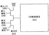
图10例示了具有分开的触摸驱动器和LCD驱动器芯片的触摸屏LCD的框图。10 illustrates a block diagram of a touch screen LCD with separate touch driver and LCD driver chips.
图11例示了具有集成LCD和触摸驱动器芯片的触摸屏LCD的框图。11 illustrates a block diagram of a touch screen LCD with an integrated LCD and touch driver chip.
图12例示了触摸屏LCD的基础叠层(stackup)。Figure 12 illustrates a basic stackup of a touch screen LCD.
图13例示了触摸屏LCD的一个替换实施例。Figure 13 illustrates an alternative embodiment of a touch screen LCD.
图14例示了一个电极图案。FIG. 14 illustrates an electrode pattern.
图15例示了触摸屏LCD的叠层图实施例。FIG. 15 illustrates a stack diagram embodiment of a touch screen LCD.
图16例示了图15所示的触摸屏LCD的触摸像素电路。FIG. 16 illustrates a touch pixel circuit of the touch screen LCD shown in FIG. 15 .
图17例示了被塑料盖保护的触摸感测层。Figure 17 illustrates a touch sensing layer protected by a plastic cover.
图18例示了触摸屏某个区域的输出列以及一组相交连的输出栅极。Figure 18 illustrates an output column for an area of a touch screen and a set of interconnected output gates.
图19例示了触摸屏LCD的触摸像素的布局。FIG. 19 illustrates the layout of touch pixels of a touch screen LCD.
图20例示了触摸屏LCD的一个实施例的叠层图。20 illustrates a stack-up diagram of one embodiment of a touch screen LCD.
图21例示了触摸传感器阵列。Figure 21 illustrates a touch sensor array.
图22用电缆布线(cabling)及子系统放置的顶视图和侧视图例示了概念A和B的物理实现。Figure 22 illustrates the physical implementation of Concepts A and B with top and side views of cabling and subsystem placement.
图23例示了一个示出了底部玻璃元件的可能架构的高级框图。Figure 23 illustrates a high-level block diagram showing a possible architecture of a bottom glass element.
图24例示了伸长的导电点。Figure 24 illustrates elongated conductive dots.
图25例示了触摸/LCD驱动器集成电路的高级框图。Figure 25 illustrates a high-level block diagram of the touch/LCD driver integrated circuit.
图26例示了与这里描述的各种LCD实施例结合使用的柔性印刷电路。Figure 26 illustrates a flexible printed circuit for use with the various LCD embodiments described herein.
图27例示了用于同时执行的显示更新和触摸扫描的处理。FIG. 27 illustrates a process for display update and touch scan performed simultaneously.
图28例示了开电VCST触摸驱动选项。Figure 28 illustrates the power-on VCST touch drive option.
图29例示了驱动-VCST触摸驱动选项。Figure 29 illustrates the drive-VCST touch drive option.
图30例示了在将触摸驱动用于触摸感测和LCD VCOM调制两者的情形下的电模型。Figure 30 illustrates the electrical model in the case where touch drive is used for both touch sensing and LCD VCOM modulation.
图31例示了将VSTM通过导电点连接到两侧的Cst线。Figure 31 illustrates connectingVSTM to Cst lines on both sides through conductive dots.
图32例示了触摸屏LCD的制造工艺流程。FIG. 32 illustrates a manufacturing process flow of a touch screen LCD.
图33例示了使用VCOM的单线反转(one line inversion)作为触摸激励信号。Figure 33 illustrates the use of one line inversion of VCOM as a touch actuation signal.
图34例示了触摸屏LCD的替换实施例的叠层图。Figure 34 illustrates a stack-up diagram of an alternate embodiment of a touch screen LCD.
图35例示了触摸屏LCD的制造工艺流程。FIG. 35 illustrates a manufacturing process flow of a touch screen LCD.
图36例示了用导电黑底(black matrix)替换触摸驱动层的实施例。FIG. 36 illustrates an embodiment in which the touch drive layer is replaced with a conductive black matrix.
图37例示了触摸屏LCD的实施例的电路图。37 illustrates a circuit diagram of an embodiment of a touch screen LCD.
图38例示了触摸屏LCD的叠层图。FIG. 38 illustrates a stack-up diagram of a touch screen LCD.
图39例示了触摸屏LCD的显示器像素的逐行更新。Figure 39 illustrates row-by-row updating of display pixels of a touch screen LCD.
图40例示了用于触摸屏LCD中的一组触敏显示行的触摸感测处理。Figure 40 illustrates touch sensing processing for a set of touch sensitive display lines in a touch screen LCD.
图41例示了为位于触摸屏LCD的不同区域中的三个像素检测触摸活动的处理。Figure 41 illustrates the process of detecting touch activity for three pixels located in different areas of the touch screen LCD.
图42例示了触摸屏LCD的另一个实施例的电路图。FIG. 42 illustrates a circuit diagram of another embodiment of a touch screen LCD.
图43例示了图42所示实施例的叠层图。FIG. 43 illustrates a stack-up diagram of the embodiment shown in FIG. 42 .
图44例示了用导电黑底来替换触摸传感层的实施例。Figure 44 illustrates an embodiment in which the touch sensing layer is replaced with a conductive black matrix.
图45例示了触摸屏LCD的另一个实施例的叠层图。FIG. 45 illustrates a stack-up diagram of another embodiment of a touch screen LCD.
图46例示了图55所示实施例的顶视图。FIG. 46 illustrates a top view of the embodiment shown in FIG. 55 .
图47例示了触摸屏LCD的另一个实施例。FIG. 47 illustrates another embodiment of a touch screen LCD.
图48例示了图47的实施例的等效电路。FIG. 48 illustrates an equivalent circuit of the embodiment of FIG. 47 .
图49例示了可以用于图47~48的实施例的触摸感测处理的波形。49 illustrates waveforms that may be used for touch sensing processing of the embodiments of FIGS. 47-48.
图50例示了图47的实施例的触摸屏集成的其他方面。FIG. 50 illustrates other aspects of the touch screen integration of the embodiment of FIG. 47 .
图51例示了触摸屏LCD的另一个实施例。FIG. 51 illustrates another embodiment of a touch screen LCD.
图52例示了可以用于图51和53实施例的触摸感测处理的波形。FIG. 52 illustrates waveforms that may be used for the touch sensing process of the embodiments of FIGS. 51 and 53 .
图53例示了图51实施例的等效电路。FIG. 53 illustrates the equivalent circuit of the embodiment of FIG. 51 .
图54例示了用于图51实施例的触摸屏集成的其他方面。FIG. 54 illustrates additional aspects of touch screen integration for the embodiment of FIG. 51 .
图55例示了触摸屏LCD的叠层图。FIG. 55 illustrates a stack-up diagram of a touch screen LCD.
图56例示了更新触摸屏LCD的处理。FIG. 56 illustrates the process of updating the touch screen LCD.
图57例示了用于触摸屏LCD实施例的叠层图。Figure 57 illustrates a stack-up diagram for a touch screen LCD embodiment.
图58例示了用于触摸屏LCD实施例的叠层图。Figure 58 illustrates a stack-up diagram for a touch screen LCD embodiment.
图59例示了被分成了可以独立更新或是实施触摸扫描的三个区域的示例性LCD显示器。59 illustrates an exemplary LCD display divided into three regions that can be independently updated or perform touch scanning.
图60例示了具有三个区域的触摸屏LCD的更新和触摸扫描处理。Figure 60 illustrates the update and touch scan process for a touch screen LCD with three areas.
图61例示了触摸屏LCD的电极布局。FIG. 61 illustrates the electrode layout of a touch screen LCD.
图62例示了触摸屏LCD的电路元件。FIG. 62 illustrates circuit elements of a touch screen LCD.
图63例示了触摸屏LCD的更新装置的快照。Figure 63 illustrates a snapshot of an update device for a touch screen LCD.
图64例示了如何将ITO中的金属线和间隙完全或者部分隐藏在黑底后面。Figure 64 illustrates how the metal lines and gaps in the ITO can be completely or partially hidden behind a black matrix.
图65例示了触摸屏LCD的叠层图。Figure 65 illustrates a stack-up diagram of a touch screen LCD.
图66例示了被分段成三个区域的触摸屏LCD。Figure 66 illustrates a touch screen LCD segmented into three regions.
图67例示了用于在触摸屏LCD中执行显示更新和触摸扫描的处理。FIG. 67 illustrates a process for performing display update and touch scan in a touch screen LCD.
图68例示了将触摸屏LCD分段成三个区域的接线及ITO布局。Figure 68 illustrates the wiring and ITO layout for segmenting the touch screen LCD into three regions.
图69例示了包含保护迹线的触摸屏LCD的某一区域的顶视图和截面图。Figure 69 illustrates a top view and a cross-sectional view of a region of a touch screen LCD containing guard traces.
图70例示了不包含保护迹线的触摸屏LCD的某一区域的顶视图和截面图。70 illustrates a top view and a cross-sectional view of a region of a touch screen LCD that does not contain guard traces.
图71例示了包含了六个触摸像素及其信号接线的示例性显示区域。Figure 71 illustrates an exemplary display area containing six touch pixels and their signal connections.
图72例示了用于触摸屏LCD的另一个实施例的叠层图。FIG. 72 illustrates a stack-up diagram of another embodiment for a touch screen LCD.
图73例示了用于触摸屏LCD的另一个实施例的叠层图。FIG. 73 illustrates a stack-up diagram of another embodiment for a touch screen LCD.
图74例示了突显了用于触摸屏LCD的VCOM信号耦合的电路图。Figure 74 illustrates a circuit diagram highlighting the VCOM signal coupling for a touch screen LCD.
图75例示了一个示例性显示器。Figure 75 illustrates an exemplary display.
图76例示了用于触摸屏LCD的可能扫描图案。Figure 76 illustrates a possible scan pattern for a touch screen LCD.
图77例示了用于图79实施例的电路图。FIG. 77 illustrates a circuit diagram for the embodiment of FIG. 79 .
图78例示了分段ITO层。Figure 78 illustrates a segmented ITO layer.
图79例示了用于触摸屏LCD的另一个实施例的叠层图。Figure 79 illustrates a stack-up diagram of another embodiment for a touch screen LCD.
图80例示了用于图79实施例的组合的接线和叠层图。Figure 80 illustrates a combined wiring and stackup diagram for the Figure 79 embodiment.
图81例示了图79实施例的物理实现方式。Figure 81 illustrates a physical implementation of the Figure 79 embodiment.
图82例示了平面转换型的LCD单元。FIG. 82 illustrates an LCD cell of the plane switching type.
图83例示了用于平面转换型LCD单元的电极组织。FIG. 83 illustrates electrode organization for an in-plane switching type LCD cell.
图84例示了用于基于IPS的触摸屏LCD的实施例的电路图。84 illustrates a circuit diagram of an embodiment for an IPS-based touch screen LCD.
图85例示了与图84相对应的叠层图。FIG. 85 illustrates a stack-up diagram corresponding to FIG. 84 .
图86例示了用于基于IPS的触摸屏LCD的另一个实施例的叠层图。Figure 86 illustrates a stack-up diagram for another embodiment of an IPS-based touch screen LCD.
图87例示了用于概念F的物理模型,也就是基于IPS的触摸屏LCD的实施例。Figure 87 illustrates a physical model for Concept F, an embodiment of an IPS based touch screen LCD.
图88例示了与图87的实施例相对应的叠层图。FIG. 88 illustrates a stack-up diagram corresponding to the embodiment of FIG. 87 .
图89例示了全玻璃触摸屏LCD的侧视图。Figure 89 illustrates a side view of an all glass touch screen LCD.
图90例示了包含塑料层的触摸屏LCD的侧视图。90 illustrates a side view of a touch screen LCD including a plastic layer.
图91例示了具有多个塑料层的触摸屏。Figure 91 illustrates a touch screen with multiple plastic layers.
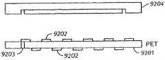
图92例示了具有在两侧图案化的PET层并且具有通过PET层的连接的触摸屏。92 illustrates a touch screen with PET layers patterned on both sides and with connections through the PET layers.
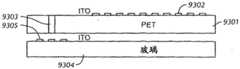
图93例示了组合PET/玻璃触摸屏。Figure 93 illustrates a combined PET/glass touch screen.
图94例示了触摸屏LCD设备组件。Figure 94 illustrates touch screen LCD device components.
图95例示了具有在透明玻璃外壳内部图案化的触摸层的触摸屏LCD。Figure 95 illustrates a touch screen LCD with a touch layer patterned inside a transparent glass housing.
图96例示了可以与触摸屏LCD结合使用的图案化PET基底。Figure 96 illustrates a patterned PET substrate that can be used in conjunction with a touch screen LCD.
图97例示了与图96的PET基底粘合的柔性印刷电路。FIG. 97 illustrates a flexible printed circuit bonded to the PET substrate of FIG. 96 .
图98例示了贴在图97的组件上的覆盖物。FIG. 98 illustrates a covering applied to the assembly of FIG. 97 .
图99例示了玻璃上的电平移动器/解码器芯片的简化图示。Figure 99 illustrates a simplified diagram of a level shifter/decoder chip on glass.
图100例示了经修改的触摸/LCD驱动器以及外围晶体管电路。Figure 100 illustrates a modified touch/LCD driver and peripheral transistor circuit.
图101例示了完全集成的触摸/LCD驱动器的简化框图。Figure 101 illustrates a simplified block diagram of a fully integrated touch/LCD driver.
图102例示了触摸屏LCD的应用。Figure 102 illustrates the application of a touch screen LCD.
图103例示了并入了触摸屏的计算机系统的框图。103 illustrates a block diagram of a computer system incorporating a touch screen.
图104例示了可以与根据本发明的触摸屏LCD结合使用的各种电子设备和计算机系统的形状因素。Figure 104 illustrates the form factors of various electronic devices and computer systems that may be used in conjunction with a touch screen LCD according to the present invention.
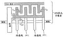
图105例示了通过连接来形成多个触摸传感列的IPS LCD子像素。Figure 105 illustrates IPS LCD subpixels connected to form multiple touch-sensing columns.
图106例示了通过连接来形成多个触摸传感行的IPS LCD子像素。Figure 106 illustrates IPS LCD sub-pixels connected to form multiple touch-sensing rows.
图107例示了集成了触摸感测处理的IPS LCD。Figure 107 illustrates an IPS LCD with integrated touch sensing processing.
具体实施方式Detailed ways
为使本领域技术人员能够获得和使用本发明,现给出如下描述,该描述是在特定应用及其需求的上下文中提供的。对本领域技术人员来说,针对所公开实施例的各种修改都是显而易见的,此外,这里定义的一般原理也可以应用于其他实施例和应用,而不会脱离本发明的精神和范围。由此,本发明并不局限于所示实施例,相反,它依照的是与权利要求相符合的最广阔的范围。To enable any person skilled in the art to make and use the present invention, the following description is now provided in the context of a particular application and its requirements. Various modifications to the disclosed embodiments will be readily apparent to those skilled in the art, and the generic principles defined herein may be applied to other embodiments and applications without departing from the spirit and scope of the invention. Thus, the present invention is not limited to the embodiments shown, but rather is to be accorded the widest scope consistent with the claims.
1.LCD和触摸感测的背景1. Background of LCD and touch sensing
在这里公开的是将触摸感测技术集成在液晶显示器中的技术。Disclosed herein are techniques for integrating touch sensing technology in a liquid crystal display.
正如本领域技术人员所了解的那样,LCD包括多个层,其中最基本的是顶部玻璃、液晶和底部玻璃。顶部和底部玻璃可以图案化,以便提供包含了特定显示器像素液晶的单元所具有的边界。顶部和底部玻璃还可以用不同导电材料层以及薄膜晶体管图案化,以便能够通过改变液晶单元两端的电压来操纵液晶的方向,由此控制像素颜色和亮度。As those skilled in the art will appreciate, an LCD includes a number of layers, the most basic of which are a top glass, a liquid crystal, and a bottom glass. The top and bottom glass can be patterned to provide the boundaries of the cells containing the liquid crystal of a particular display pixel. The top and bottom glass can also be patterned with layers of different conductive materials, as well as thin-film transistors, so that the direction of the liquid crystal can be manipulated by changing the voltage across the liquid crystal cell, thereby controlling pixel color and brightness.
正如作为参考引入的申请中描述的那样,对触摸表面、尤其是具有多点触摸能力的透明触摸表面来说,该表面可以由一系列层形成。这一系列层可以包括至少一个基底,例如玻璃,并且在该基底上可以布置多个触敏电极。例如,互电容装置可以包括用玻璃这类非导电层分开的多个驱动电极和多个传感电极。当有导电物体(例如用户手指)接近时,驱动电极与传感电极之间的电容耦合有可能会受到影响。这种电容耦合变化可以用于确定特定触摸的位置、形状、大小、运动、标识等等。然后,通过解释这些参数,可以控制计算机或其他电子设备的操作。对本领域技术人员来说,下述自电容装置同样是已知的。For a touch surface, especially a transparent touch surface with multi-touch capability, the surface may be formed of a series of layers, as described in the application incorporated by reference. The series of layers may include at least one substrate, such as glass, on which a plurality of touch-sensitive electrodes may be arranged. For example, a mutual capacitance device may include multiple drive electrodes and multiple sense electrodes separated by a non-conductive layer such as glass. When a conductive object (such as a user's finger) approaches, the capacitive coupling between the drive electrode and the sense electrode may be affected. This capacitive coupling change can be used to determine the location, shape, size, motion, identity, etc. of a particular touch. Then, by interpreting these parameters, the operation of a computer or other electronic device can be controlled. The following self-capacitance devices are likewise known to those skilled in the art.
通过集成LCD和触摸传感器的分层结构,可以实现多种益处。该集成可以包括组合或交错上述分层结构。此外,该集成还可以包括省去冗余结构和/或发现特定层或结构的双重用途(例如一个用途为触摸功能而另一个用途为显示功能)。这样做可以允许省去某些层,由此降低触摸屏LCD的成本和厚度,以及简化制造过程。目前,可能有多种不同的装置,并且在这里将会进一步详细描述这其中的某些装置。Multiple benefits can be achieved by integrating the layered structure of the LCD and touch sensor. This integration may include combining or interleaving the above-described hierarchies. Additionally, the integration may also include eliminating redundant structures and/or finding dual uses of particular layers or structures (eg, one use for touch functionality and the other for display functionality). Doing so may allow certain layers to be omitted, thereby reducing the cost and thickness of the touch screen LCD, as well as simplifying the manufacturing process. Presently, a number of different arrangements are possible, some of which will be described in further detail herein.
特别地,在下文中将会论述集成触摸屏LCD的各个实施例。但是本领域技术人员将会了解,这里关于附图给出的详细描述是例示性而不是穷举性的,而且针对这些实施例的众多变化都是可能的。此外,虽然所公开的很多实施例涉及的是具有多点触摸能力的装置,但是众多教导也可以应用于单点触摸显示器。In particular, various embodiments of the integrated touch screen LCD will be discussed below. However, those skilled in the art will appreciate that the detailed description given herein with respect to the accompanying drawings is illustrative and not exhaustive, and that numerous variations to the embodiments are possible. Additionally, while many of the disclosed embodiments relate to devices with multi-touch capabilities, many of the teachings can also be applied to single-touch displays.
1.1多点触摸感测1.1 Multi-touch sensing
借助图1所示的多点触摸感测装置,可以识别多个同时或几乎同时的触摸事件。多点触摸感测装置100可以检测和监视在同一时间、在接近同一时间、在不同时间或是在某个时段上在触敏表面101上出现的多个触摸属性(包括例如标识、位置、速度、大小、形状和幅度)。触敏表面101可以提供以彼此基本独立的方式起作用并且代表了触敏表面上的不同点的多个传感器点、坐标或节点102。感测点102可以位于某个网格或像素阵列中,其中每个感测点都能同时产生一个信号。感测点102可以被认为是将触敏表面101映射到了一个坐标系,例如笛卡尔或极坐标系。With the multi-touch sensing device shown in FIG. 1, multiple simultaneous or nearly simultaneous touch events can be recognized. The
举例来说,触敏表面可以采用平板或触摸屏的形式。为了生产触摸屏,可以使用基本透明的导电介质,例如氧化铟锡(ITO)。感测点102的数量和配置是可以改变的。通常,感测点102的数量取决于期望分辨率和灵敏度。在触摸屏应用中,感测点102的数量还可以取决于触摸屏的期望透明度。For example, the touch-sensitive surface may take the form of a tablet or a touch screen. For the production of touchscreens, substantially transparent conductive media such as indium tin oxide (ITO) can be used. The number and configuration of sensing
通过使用与下文详述相类似的多点触摸感测装置,可以使用在多点触摸传感器101的节点102上生成的信号来产生特定时间点的触摸图像。例如,与触敏表面101接触或在其附近的每个物体(例如手指、指示笔等等)都可以产生图2所示的接触印迹区域201。每一个接触印迹区域201都有可能覆盖若干个节点102。被覆盖的节点202可以检测到物体,而剩余节点102则不会检测到物体。由此可以形成触摸表面平面的像素化图像(pixilatedimage)(该图像可以被称为触摸图像、多点触摸图像或接近度图像)。每一个接触印迹区域201的信号都可以聚集在一起。每一个接触印迹区域201都可以包括以每一个点的触摸量为基础的高点和低点。接触印迹区域201的形状以及图像内部的高点和低点可以用于区分彼此接近的接触印迹区域201。此外,当前图像还可以与先前图像相比较,以便确定物体如何随时间移动,以及确定据此在主机设备中应该执行怎样的对应操作。Signals generated on
有很多种不同的感测技术可以与这些感测装置结合使用,其中包括电阻、电容、光学感测装置等等。在基于电容的感测装置中,当物体趋近于触敏表面101时,在该物体与接近该物体的感测点102之间将会形成一个小电容。通过检测这一小电容在每个感测点102引起的电容变化,以及通过记录感测点的位置,感测电路103可以检测和监视多个触摸活动。对电容感测节点来说,它既可以基于自电容,也可以基于互电容。There are many different sensing technologies that can be used in conjunction with these sensing devices, including resistive, capacitive, optical sensing devices, and the like. In capacitance-based sensing devices, as an object approaches the touch-
在自电容系统中,感测点“自身”的电容是相对于诸如地面之类的某个基准测量的。感测点102可以是空间分开的电极。这些电极可以通过导电迹线105a(驱动线)和105b(传感线)耦合至驱动电路104和感测电路103。在某些自电容实施例中,与每个电极相连的单个导电迹线可以同时用作驱动线和传感线。In a self-capacitance system, the capacitance of the sensing point "self" is measured relative to some reference such as ground. The sensing points 102 may be spatially separated electrodes. These electrodes may be coupled to drive
在互电容系统中,第一电极与第二电极之间的“相互”电容可被测量。在互电容感测装置中,这些感测点可以由形成空间分开的线路的图案化导体的交叉来形成。例如,在第一层可以形成驱动线105a,而在第二层105b上则可以形成感测线105b,由此,驱动线和传感线彼此会在感测点102处交叉或“相交”。不同的层可以是不同基底,同一基底的不同侧面,或是具有一定介电分离度的同一基底侧面。由于驱动线与传感线之间是分开的,因此,每一个“相交”处都有可能存在电容耦合节点。In a mutual capacitance system, the "mutual" capacitance between a first electrode and a second electrode can be measured. In mutual capacitance sensing devices, these sensing points may be formed by the intersection of patterned conductors forming spatially separated lines. For example,
驱动线和传感线的布置是可以改变的。例如,在笛卡尔坐标系中(如图所示),驱动线可以形成为水平行,而传感线可以形成为垂直列(反之亦然),于是就可以形成能被认为具有不同的x坐标和y坐标的多个节点。作为替换,在极坐标系中,传感线可以是多个同心圆,而驱动线则是径向延伸的线(反之亦然),于是就形成能被认为具有不同的径坐标和角坐标的多个节点。无论哪一种情况,驱动线105a都可以与驱动电路104相连,并且感测线105b可以与感测电路103相连。The arrangement of drive and sense lines can be varied. For example, in a Cartesian coordinate system (as shown), the drive lines can be formed as horizontal rows and the sense lines can be formed as vertical columns (or vice versa), thus forming what can be considered to have different x-coordinates and multiple nodes with y coordinates. Alternatively, in a polar coordinate system, the sensing lines can be concentric circles and the drive lines are radially extending lines (or vice versa), thus forming what can be considered to have different radial and angular coordinates multiple nodes. In either case, the
在操作过程中,在每一条驱动线105a上都可以施加驱动信号(例如周期性电压)。在驱动时,施加于驱动线105a的电荷可以通过节点102电容性地耦合至相交的传感线105b。这会引起在传感线105b中产生可检测、可测量的电流和/或电压。对驱动信号和在传感线105b上出现的信号来说,它们之间的关系可以是驱动线和传感线的电容耦合的函数,其中如上所述,该电容耦合有可能受到接近节点102的物体的影响。如下文更详细描述的那样,感测线105b可以由一个或多个电容感测电路103来感测,并且可以确定每一个节点处的电容。During operation, a drive signal (eg, a periodic voltage) may be applied to each of the
如上所述,每次可以驱动一条驱动线105a,同时其他驱动线则被接地。可以为每一条驱动线105a重复执行该处理,直至所有驱动线已被驱动并且能从感测的结果中构建(基于电容的)触摸图像为止。一旦所有线路105a都已被驱动,则可以重复执行该序列,以便构建一系列触摸图像。但是,在本发明的某些实施例中也可以基本同时或几乎同时地驱动多条驱动线。As described above, one
图3例示了与上述装置相对应的互电容电路300的简化示意图。互电容电路300可以包括驱动线105a和传感线105b,这些线可以是空间分开的,由此形成电容耦合节点102。驱动线105a可以电(即,导电地)耦合到电压源310所代表的驱动电路104。传感线105b可以电耦合到电容感测电路103。在某些情况下,驱动线105a和传感线105b均有可能包括些许寄生电容302。FIG. 3 illustrates a simplified schematic diagram of a
如上所述,如果在驱动线105a和感测线105b相交处附近没有导电物体,那么节点102处的电容耦合可以保持相当稳定。但如果在节点102附近出现导电物体(例如用户手指、指示笔等等),那么电容耦合(即局部系(local system)的电容)将会改变。电容耦合的这种变化将会改变传感线105b携有的电流(和/或电压)。电容感测电路103可以记录这个电容变化以及节点102的位置,并将该信息按某种形式报告给处理器106(图1)。As mentioned above, if there are no conductive objects near where the
参考图1,感测电路103可以从触摸表面101获取数据,并且将所获取的数据提供给处理器106。在某些实施例中,感测电路103可以被配置成向处理器106发送原始数据(例如与每一个传感点102相对应的电容阵列值)。在其他实施例中,感测电路103可以被配置成自己处理原始数据,并且将经过处理的触摸数据递送到处理器106。无论发生哪一种情况,处理器于是便可以使用其接收的数据来控制计算机系统107的操作和/或在其上运行的一个或多个应用。在上文引用的申请中描述了沿着这些线的各种实现,并且这些实现包括具有触摸板和触摸屏的各种计算机系统。Referring to FIG. 1 , the
在某些实施例中,感测电路103可以包括一个或多个微控制器,其中每一个微控制器都可以监视一个或多个感测点102。这些微控制器可以是专用集成电路(ASIC),其中该电路通过与固件合作来监视源自触敏表面101的信号,处理所监视的信号,以及将该信息报告给处理器106。微处理器还可以是数字信号处理器(DSP)。在某些实施例中,感测电路103可以包括一个或多个传感器IC,其中所述一个或多个传感器IC对每一条感测线105b中的电容进行测量,并且将测得的值报告给计算机系统107内的处理器106或主机控制器(未示出)。可以使用任何数量的传感器IC。例如,传感器IC可以用于所有线路,或者多个传感器IC可以用于单条线路或线路组。In some embodiments, the
图4例示了用于操作与上文描述相类似的多点触摸感测装置的高级处理400。该处理以其中驱动多个感测点102的方框401为开始。在方框401之后,处理流程可以前进到其中可以读取感测点102的输出的方框402。例如,可以获取每一个感测点102的电容值。在方框402之后,该处理前进到方框403,其中可以产生某个触摸在某个时刻的图像或其他数据形式(一个或多个信号),此后则可以对其进行分析,以便确定触摸或是接近该触摸传感器的物体所在的位置。在方框403之后,该处理可以前进到方框404,其中可以将当前图像或信号与一个或多个过去的图像或信号相比较,以便为每一个物体确定形状、大小、位置、方向、速度、加速度、压力等等中的一项或多项的变化。随后,通过使用该信息(在步骤405),可以在计算机系统107中执行一动作,该动作可以是从移动指针或光标到基于复杂手势的交互。FIG. 4 illustrates a high-
1.2.半透式反射LCD1.2. Transflective LCD
在这里给出了对半透式反射LCD的简要介绍,以便帮助更好地理解将触摸感测技术与半透式反射LCD相集成的处理。在下文中概述了可以在低温多晶硅(LTPS)的半透式反射LCD中发现的典型子像素单元。A brief introduction to transflective LCDs is given here to help better understand the process of integrating touch sensing technology with transflective LCDs. Typical sub-pixel cells that may be found in a low temperature polysilicon (LTPS) transflective LCD are outlined below.
1.2.1电路基础1.2.1 Circuit Fundamentals
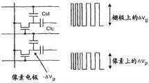
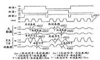
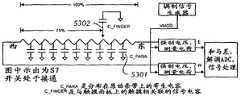
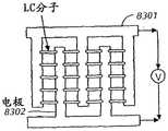
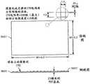
图5示出了LTPS半透式反射子像素500的代表性布局。在将代表期望灰度值(greylevel)的电压施加于数据总线501,以及在选择线502被断言(assert)时,显示信息可以被传送到子像素电容器CST和CLC(未示出)。选择线502的断言电平(assertion level)可以接近于栅极驱动正向供给电压。在选择线502被断言的时段中,VCST(以及未示出的VCOM)上的电压可以是恒定的。包括金属、聚乙烯、有源的、氧化物和ITO在内的图5所示的所有电路部件都可以在LCD的底部玻璃上制作。FIG. 5 shows a representative layout of an
图6示出了低温多晶硅(LTPS)LCD 600的简化模型,其中包括顶视图601和侧视图602。顶视图601示出了同时位于显示区域604和非显示区域605内的底部玻璃608上的VCST布线(routing)603的透视图(see-through view)。侧视图602示出了显示器的横截面。FIG. 6 shows a simplified model of a low temperature polysilicon (LTPS)
每一个显示行都可以包括用于VCST 606的水平迹线和选择迹线(未示出)。该选择迹线与同样未示出的、由多晶硅薄膜晶体管(p-Si TFT)制成的栅极驱动电路相连。VCST迹线606可以从显示器边缘延伸至显示器边缘,并且可以如左侧所示的那样连接在一起。这些VCST迹线也可通过导电点607连接到顶部玻璃610上的ITO平面609。一般而言,可以使用分别位于四个角的四个导电点来将VCOM平面连接到VCOMDrive(VCOM驱动)611。为了简单起见,图6只示出一个点607。VCST和顶部玻璃ITO 609的电压可以由VCOMDrive设置,其中所述VCOMDrive可以由LCD驱动器IC(未示出)提供。此外,VCST也可以与VCOMDrive 611之外的另一个驱动源相连。Each display row may include horizontal and select traces (not shown) forVCST 606 . The select traces are connected to gate drive circuits, also not shown, made of polysilicon thin film transistors (p-Si TFTs).VCST traces 606 may extend from display edge to display edge and may be connected together as shown on the left. TheseVCST traces can also be connected to the
图7例示了子像素的电路图700,并且示出了各种元件可以在哪个玻璃基底上制作。底部玻璃701可以是用于集成所有TFT像素电路703的基底。这可以包括选择线驱动器和控制逻辑。底部玻璃还可以为诸如LCD驱动器(未示出)之类的玻璃上芯片(COG)元件充当基底。电容器CLC的上部电极704可以位于玻璃702的顶部。电极704可以是覆盖整个显示区域并且形成连至底部电极705的反电极(counter electrode)以造成CLC的ITO平面。上部电极704还可以与底部玻璃701上的VCOMDrive 701相连,例如通过位于四角的导电点706(只示出了一个)来连接。FIG. 7 illustrates a circuit diagram 700 of a subpixel and shows on which glass substrate the various components may be fabricated.
1.2.2.VCOM1.2.2.VCOM
通过最小化或消除液晶(LC)两端电压的DC分量,可以减小或消除某些非期望的图像伪像。由此,LC两端的电场可以周期性翻转,同时在两个场方向上保持整体平衡。要想获取完美的电场平衡是非常困难的,这样做有可能导致产生较小的DC偏移量,并且该偏移量将会产生不想要的图像伪像。为了屏蔽DC偏移量导致的闪烁,可以利用本领域技术人员已知的若干种反转方案之一,例如点反转。By minimizing or eliminating the DC component of the voltage across the liquid crystal (LC), certain undesired image artifacts can be reduced or eliminated. Thereby, the electric field across the LC can be periodically flipped while maintaining overall balance in the two field directions. Achieving a perfect electric field balance is very difficult, and doing so may result in a small DC offset that will produce unwanted image artifacts. To mask the flicker caused by the DC offset, one of several inversion schemes known to those skilled in the art can be utilized, such as dot inversion.
1.2.3调制VCOM1.2.3 Modulation VCOM
在某些实施例中,较为理想的是减小数据驱动器的电压范围。因此,可以将VCOMITO平面和VCST迹线从接地调制到供电轨,以便产生LC两端的AC电压。但是,这样做有可能会将可用反转方法局限于帧和线路类型。In some embodiments, it may be desirable to reduce the voltage range of the data driver. Therefore, the VCOM ITO plane and VCST traces can be modulated from ground to the supply rails in order to produce an AC voltage across the LC. However, doing so may limit the available inversion methods to frame and line types.
VCOMDrive的需求可以相对简单:其电压可以保持恒定直到某一行像素的电荷传送完成,由此设置该行像素的灰度值。一旦设置了显示器像素,倘若出入子像素的寄生路径仍旧较小,那么VCOMDrive就可以在不显著影响LC状态的情况下改变。The requirements of the VCOM Drive can be relatively simple: its voltage can be kept constant until the charge transfer of a row of pixels is completed, thereby setting the gray value of the row of pixels. Once a display pixel is set up, VCOM Drive can be changed without significantly affecting the LC state, provided the parasitic paths to and from the sub-pixel are still small.
1.2.4恒定VCOM1.2.4 Constant VCOM
VCOM调制有可能会使触摸感测和LCD的集成变得复杂。在下文中将会论述用于克服这些复杂性的各种技术。可以利用一种将液晶两端电压的DC分量减至最小的替换方法。在J.Hector和P.Buchschacher发表于SID 02Digest第695~697页的“Low Power DrivingOptions for an AMLCD Mobile Display Chipset”一文中描述了一种这样的替换方法,该文在此被引入作为参考。此替换方法可以允许VCOM保持在恒定电压上,而不需要大电压范围的数据驱动器,并且功耗可以很低。在下文中将会描述使用恒定VCOM的各种优点。VCOM modulation has the potential to complicate touch sensing and LCD integration. Various techniques for overcoming these complexities are discussed below. An alternative method of minimizing the DC component of the voltage across the liquid crystal can be used. One such alternative is described in the article "Low Power Driving Options for an AMLCD Mobile Display Chipset" by J. Hector and P. Buchschacher, SID 02Digest, pp. 695-697, which is incorporated herein by reference. This alternative method can allow VCOM to remain at a constant voltage without the need for a wide voltage range data driver, and the power consumption can be low. Various advantages of using a constant VCOM will be described below.
1.3LCD制造1.3 LCD Manufacturing
LCD面板的制造可以通过对被称为母玻璃(mother-glass)的大片玻璃使用分批工艺来完成。可以使用两片母玻璃:可以为滤色器、黑底以及CLC的上部电极提供基底的顶部母玻璃;以及可以为有源矩阵TFT阵列和驱动电路提供基底的底部母玻璃。The manufacture of LCD panels can be done by using a batch process with large sheets of glass called mother-glass. Two mother glasses can be used: a top mother glass, which can provide the substrate for the color filters, black matrix, and upper electrodes of the CLC ; and a bottom mother glass, which can provide the substrate for the active matrix TFT array and driver circuits.
在图8中显示了一个用于制造LCD的基本处理流程800。这两大片母玻璃一片用于LCD顶部一片用于底部,它们在对准(方框803)、压制到一起以及加热(方框804)以固化顶部玻璃和底部玻璃之间的密封籍此产生稳定的面板结构之前各自可以经历处理步骤801和802。然后,大面板可被划片并分成期望尺寸的较小模块(方框805)。在用液晶填充独立模块(方框807)之前,这些模块的边缘可以被研磨(方框806)。在填充之后,该模块可被密封(方框809)。偏振器和电子元件可以被附着(方框809)。在处理结束或是接近于处理结束的时候,柔性印刷电路(FPC)可以附着于其基底。A
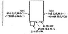
在图9中示出了一个已完成的LCD模块900。所示的LCD模块包括附着于底部玻璃902的玻璃上芯片(COG)LCD驱动器901,并且还包括附着于底部玻璃902的玻璃上柔性板(flex on glass,FOG)柔性印刷电路(FPC)903。这两个元件可以电连接至底部玻璃焊盘,并且可以使用各向异性的导电胶(ACA)保持在原地。底部玻璃902可以延伸到顶部玻璃904之外,以便提供支架来安装COG LCD驱动器901、FPC 903以及其他支撑元件。对手持设备来说,为LCD管理数据并提供控制的系统处理器底板可以放置在背光灯906的下方。A completed
用于支持触摸感测的附加元件(例如FPC)同样可以附着于支架905。此外,其他附着点同样是可以能的。在下文中将会结合相关实施例来论述这些细节。Additional elements (eg, FPCs) for supporting touch sensing may also be attached to the
1.4组合LCD和触摸感测1.4 Combining LCD and touch sensing
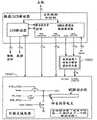
通过结合图10和11的框图,可以更好地理解这里论述的叠层图。从顶部开始,触摸传感电极1001、1101可以沉积在LCD顶部玻璃1002、1102的顶部上(用户一侧)。触摸驱动电极1003、1103可以在顶部玻璃1002、1102的底侧图案化。导电点1004、1104可以将驱动电极1003、1103连接到同样位于底部玻璃1006、1106的驱动器1005、1105。底部玻璃1006、1106上的支架1007、1107可以容纳LCD驱动器芯片1008、1108以及触摸传感器驱动芯片1009,其中这些芯片既可以相互对接(图10),也可以集成在单个元件中(图11)。最后,与支架粘合的FPC 1010、1110还可以与主机设备1011、1111相连。The stack-up diagrams discussed herein can be better understood by combining the block diagrams of FIGS. 10 and 11 . Starting from the top,
2.集成选项2. Integration options
对集成了触摸感测的LCD来说,其某些实施例可以包括顶部玻璃和底部玻璃。在这两层玻璃之一和/或二者上可以形成显示器控制电路,以便影响穿过这两层玻璃层之间的液晶层的光量。顶部玻璃和底部玻璃外边缘之间的空间在此称为液晶模块(LCM)。For LCDs with integrated touch sensing, some embodiments thereof may include a top glass and a bottom glass. Display control circuitry may be formed on one and/or both of the two layers of glass to affect the amount of light passing through the liquid crystal layer between the two layers of glass. The space between the outer edges of the top glass and the bottom glass is referred to herein as a liquid crystal module (LCM).
如图12所示,典型的LCD叠层1200通常包括附加层。在图12中,硬涂层的PMMA层1201可以保护LCD偏振器1202和顶部玻璃1203,并且在底部玻璃1204与背光1206之间可以包括第二偏振器1205。As shown in FIG. 12, a
将触摸感测技术集成在LCD中的处理可以用多种技术实现。例如,可以将不同的触摸感测部件和/或层并入LCD显示器,其中不同实施例会在显示器和/或制造成本、显示大小、显示复杂度、显示持续时间、显示功能以及图像显示质量这些因素上有所不同。在某些实施例中,触摸感测能力是通过将触摸感测部件集成在LCM之外的LCD显示器上而被包括在LCD内的。在其他实施例中,触摸感测部件也可以同时添加在LCM内部(例如两玻璃层之间)和LCM外部。在其他一些实施例中,可以只在LCM内部添加一组触摸感测部件(例如在两玻璃层之间)。后续章节将会描述用于上述每一个实施例的几个概念。The process of integrating touch sensing technology in an LCD can be implemented in a variety of technologies. For example, different touch-sensing components and/or layers may be incorporated into an LCD display, with different embodiments depending on factors such as display and/or manufacturing cost, display size, display complexity, display duration, display functionality, and image display quality above is different. In some embodiments, touch sensing capability is included within the LCD by integrating touch sensing components on the LCD display outside of the LCM. In other embodiments, touch sensing components may also be added both inside the LCM (eg, between two glass layers) and outside the LCM. In other embodiments, only one set of touch sensing components may be added inside the LCM (eg, between two glass layers). Subsequent sections will describe several concepts used in each of the above-described embodiments.
2.1液晶模块外部的触摸感测2.1 Touch Sensing Outside the LCD Module
通过将触摸感测部件添加在LCM外部,可以允许为LCD显示器添加触摸感测能力,同时对典型的LCD制造实践不产生影响或影响甚微。例如,触摸感测系统和LCD显示器系统可以被分开制作,并且在最后一个步骤中集成,从而形成具有触摸感测能力的LCD。此外,通过将触摸感测部件包括在LCM的外部,还可以允许将触摸感测部件放置在与用户触摸区域接近的位置,由此可以降低显示器与触摸元件之间的电干扰。By adding touch-sensing components outside the LCM, it may allow for the addition of touch-sensing capabilities to LCD displays with little or no impact on typical LCD manufacturing practices. For example, the touch sensing system and the LCD display system can be fabricated separately and integrated in a final step to form an LCD with touch sensing capabilities. Furthermore, by including the touch-sensing components outside the LCM, it may also allow the touch-sensing components to be placed in close proximity to the user's touch area, thereby reducing electrical interference between the display and the touch elements.
标识为概念C和概念N的以下两个实施例可以并入这种外部触摸感测元件。The following two embodiments, identified as Concept C and Concept N, may incorporate such external touch sensing elements.
2.1.1概念C2.1.1 Concept C
本发明的一个实施例是概念C,它使用的是图13所示的叠层,由此允许与LCD分开的触摸功能。在概念C中,在滤色器(CF)板(例如顶部玻璃层)顶部可以图案化两个附加的氧化铟锡(ITO)层(ITO1 1301和ITO2 1302)。这些层可用于触摸传感器的触摸传感和触摸驱动部件,其中所述触摸传感器可以是互电容触摸传感器。这些ITO层可以被图案化成列和/或行(在图1和2中示出且在先前的多点触摸感测描述中有所描述),并且可以由电介质分开,诸如由玻璃基底或是薄(例如5~12mm)SiO2层分开。One embodiment of the present invention is Concept C, which uses the stack-up shown in Figure 13, thereby allowing touch functionality separate from the LCD. In Concept C, two additional indium tin oxide (ITO) layers (
在某些实施例中,通过优化触摸部件中使用的电极图案,可以减少视觉伪像。例如,图14例示了一个可以减小视觉伪像的菱形电极图案。In certain embodiments, visual artifacts may be reduced by optimizing the electrode patterns used in the touch components. For example, Figure 14 illustrates a diamond-shaped electrode pattern that reduces visual artifacts.
在概念C中,携有触摸感测数据的FPC可以附着在顶部玻璃1303的顶面。In Concept C, the FPC carrying the touch sensing data can be attached to the top surface of the
2.1.2概念N2.1.2 Concept N
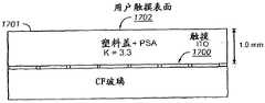
本发明的一个实施例是概念N,它可以在滤色器(CF)板的外表面上使用自电容感测来实现电容感测。概念N可以使用图15所示的叠层,其中触摸感测元件可以位于CF板1501的顶部(顶部玻璃)。通过使用例如与常规TFT板1504工艺相同的LTPS工艺在CF板1501上形成具有两个金属层的TFT 1503以及图案化ITO 1500,可以在不改变标准LCD工艺的情况下构造基于概念N的LCD。触摸ITO层1500可以被图案化成多个触摸像素1612(图16)。该触摸ITO层1500可以用塑料盖(如图17所示)保护,并且该塑料盖还可以充当由用户触摸的表面。One embodiment of the present invention is Concept N, which enables capacitive sensing using self-capacitance sensing on the outer surface of a color filter (CF) plate. Concept N can use the stackup shown in Figure 15, where the touch sensing elements can be on top of the CF board 1501 (top glass). By forming
图16例示了一个用于概念N的自电容触摸像素电路。每个ITO触摸像素1612都可以与两个TFT相连,例如一输入TFT 1604和一输出TFT 1608。输入TFT 1604可以为ITO触摸像素1612充电,输出TFT 1608则可以为ITO触摸像素1612放电。所移动的电荷量可以取决于ITO触摸像素1612的电容,其中该电容可以按照手指的接近度改变。关于自电容触摸感测的更多细节在上文以及在2001年11月27日提交的名为“Method and Apparatus forIntegrating Manual Input”的美国专利6,323,846中有所描述,其中该专利在这里全部引入作为参考。Figure 16 illustrates a self-capacitance touch pixel circuit for Concept N. Each
在一个实施例中,如图16和18中就输出列1610‘C0’和输出栅极1606‘R3’所显示的那样,输出列1610可以由垂直方向上的触摸像素共享,并且输出栅极1606可以由水平方向上的触摸像素共享。图19示出了触摸像素的详细布局。In one embodiment, as shown in FIGS. 16 and 18 for output column 1610 'C0' and output gate 1606 'R3', output column 1610 may be shared by touch pixels in the vertical direction, and
2.2部分集成的触摸感测2.2 Partially Integrated Touch Sensing
在LCM内部集成触摸感测部件可以提供多种优点。例如,添加在LCM内部的触摸感测部件可以“重新使用”本来仅用于显示功能的ITO层或其他结构来提供触摸感测功能。通过将触摸感测特征并入现有显示层,还可以减少总层数,从而减小显示器厚度并且简化制造工艺。Integrating touch-sensing components within the LCM can provide several advantages. For example, touch-sensing components added inside the LCM can "reuse" an ITO layer or other structures that would otherwise be used only for display functions to provide touch-sensing functions. By incorporating touch sensing features into existing display layers, the overall number of layers can also be reduced, thereby reducing display thickness and simplifying the manufacturing process.
以下实施例可以包括处于LCM内部和外部的触摸感测部件。由于将触摸感测部件集成在LCM内可能导致这两种功能之间出现噪声和干扰,因此,以下设计还可以包括那些允许共享各部件同时还减小或消除显示器和/或触摸感测之间的电干扰对这两者输出的负面影响的技术。The following embodiments may include touch sensing components inside and outside the LCM. Since integrating touch-sensing components within the LCM may result in noise and interference between these two functions, the following designs may also include those that allow sharing of components while also reducing or eliminating the interaction between the display and/or touch-sensing technology that negatively affects the output of both electrical disturbances.
2.2.1概念A2.2.1 Concept A
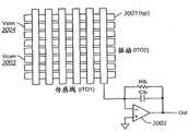
概念A可以在顶部玻璃与偏振器2003之间使用图20所示的基础叠层2000,其中具有多点触摸(“MT”)能力的ITO传感层(ITO1)2001位于顶部玻璃2002的用户一侧。从顶部开始,触摸感测层可以包括:ITO1 2001(可以被图案化成N条传感(或驱动)线的ITO层)以及ITO2 2004(可以被图案化成M条驱动(或传感)线的ITO层)。ITO2 2004还可以充当LCD的VCOM电极。Concept A can use the
2.2.1.1概念A:触摸传感器电极2.2.1.1 Concept A: Touch Sensor Electrodes
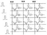
触摸传感器电极阵列可以包括图21(左侧)所示的两个图案化ITO层。图21是触摸传感器电极的一种可能实现的简化视图。离观察者较近的层ITO1 2101可以是触摸输出层,也可以称为传感层或传感线。触摸驱动层2102可以位于层ITO2上。ITO2还可以形成电容器CLC(参见图7)的上部电极。此外,图21(右侧)还示出了三个传感像素2103a、2103b和2103c及其关联电容器的细节。这些传感线和驱动线都具有5mm的节距且其间隙是10~30微米。所述间隙可以足够小到肉眼不可见,但仍然大到足以很容易地用简单的接近式掩模来蚀刻(图中间隙是被夸张放大的)。The touch sensor electrode array may include two patterned ITO layers as shown in Figure 21 (left). 21 is a simplified view of one possible implementation of touch sensor electrodes. The
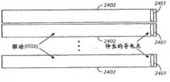
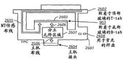
图22示出了概念A的一种可能的物理实现,包括关于电缆布线和子系统放置的顶视图2201及侧视图2202。顶视图2201示出了处于展开状态的FPC 2203的近似位置(以下将会更为详细地论述)。图22只示出了一种其中可以使用分立的触摸电平移动器/解码器COG的实现。在下文中将会论述那些将分立触摸元件的数量减至最少的替换架构。出于机械稳定性的考虑,如侧视图2202所示,FPC可以弯曲,使得施加在T-tab(顶部接头)2204和B-tab(底部接头)2205粘合处的压力最小。图23是示出了主底部玻璃元件所具有的一种可能架构2300以及位于顶部玻璃上的供触摸感测用的分段ITO2层2301的高级框图。对处于顶部玻璃上的ITO2来说,其每一个分段2302都通过导电点2303连接至底部玻璃上的相应焊盘。如下所述,底部玻璃上的每个焊盘都可以连接到触摸驱动器。Figure 22 shows one possible physical implementation of Concept A, including a
2.2.1.2概念A:导电点2.2.1.2 Concept A: Conductive Points
位于LCD各角的导电点可以用于将VCOM电极连接至驱动电路。附加的导电点可用于将触摸驱动线连接到触摸驱动电路。这些点可以具有足够低的电阻,以免显著增加触摸驱动信号的相位延迟(以下将会更详细地论述)。这可以包括将导电点电阻限制在10欧或更低。导电点大小还可以被限制以减小所需的基板面(real estate)。Conductive dots at the corners of the LCD can be used to connect the VCOM electrodes to the driver circuit. Additional conductive dots can be used to connect the touch drive lines to the touch drive circuitry. These points may have a sufficiently low resistance so as not to significantly increase the phase delay of the touch drive signal (discussed in more detail below). This can include limiting conductive point resistance to 10 ohms or less. The conductive spot size can also be limited to reduce the required real estate.
如图24所示,在这里可以使用伸长的导电点2401来减小对点电阻和基板面的要求。触摸驱动分段2402的宽度可以是约5mm,由此可以提供较大的面积来减小点电阻。As shown in Figure 24, elongated
2.2.1.3概念A:柔性电路和触摸/LCD驱动器IC2.2.1.3 Concept A: Flex Circuits and Touch/LCD Driver ICs
常规显示器(例如图9)可以具有用于控制显示器低级操作的LCD驱动器集成电路(IC)901。系统主机处理器可以通过向LCD驱动器901发送命令和显示数据来对显示器行使高级控制。多点触摸系统还可以具有一个或多个驱动器IC。在并入的参考文献中描述了一种具有多点触摸能力的示例性系统,该系统包括三个IC,即多点触摸控制器、外部电平移动器/解码器以及诸如ARM处理器的控制器。ARM处理器可以对多点触摸控制器执行低级控制,随后就可以控制电平移动器/解码器。系统主机处理器可以对ARM处理器执行高级控制并从中接收触摸数据。在某些实施例中,这些驱动器可以集成在单个IC中。A conventional display (eg, Figure 9) may have an LCD driver integrated circuit (IC) 901 for controlling low-level operation of the display. The system host processor can exercise advanced control over the display by sending commands and display data to the
图25示出了触摸/LCD驱动器集成电路2501的一个示例高级框图。该IC具有两个主要功能:1)LCD控制和更新,以及2)触摸扫描和数据处理。这两个功能可以由用于LCD控制的LCD驱动器部分2502、ARM处理器2503以及用于触摸扫描和处理的多点触摸控制器2504来集成。触摸电路可以与LCD扫描同步以免相互干扰。主机与LCD驱动器或ARM处理器之一间的通信可以通过主机数据和控制总线2505来进行。如下将论述集成得更完全的触摸/LCD驱动器。FIG. 25 shows an example high-level block diagram of the touch/LCD driver integrated
如图26所示,将用于各种触摸和显示层的信号集合到一起的FPC 2601可以具有三个连接器接头,即T-tab 2602、B-Tab 2603以及主机接头2604。T-tab可以与顶部玻璃上的传感线焊盘相连。T-tab迹线2605可以与B-tab 2603上相应的焊盘相连,而B-tab 2603也可以附着于底部玻璃。B-tab 2603还可以提供从主机接头2604到触摸/LCD驱动器IC的通过布线2606,其中主机接口2604能将主机连接至触摸/LCD驱动器IC。FPC 2601还可以为支持触摸和LCD操作的各个元件2607提供基底,并且可以通过两个焊盘2608与背光FPC相连。As shown in FIG. 26 , the
FPC 2601可以是同时与顶部和底部玻璃粘合的接头。作为替换,其他粘合方法也是可以使用的。The
2.2.1.4概念A:集成在底部玻璃上的触摸驱动2.2.1.4 Concept A: Touch driver integrated on bottom glass
电平移动器/解码器芯片连同分开的升压器(例如3V至18V升压器)一起可以提供用于触摸感测的高电压驱动电路。在一个实施例中,触摸/LCD驱动器IC可以控制电平移动器/解码器芯片。作为替换,升压器和/或电平移动器/解码器可以集成在触摸/IC驱动器IC中。例如,所述集成可以用高电压(18V)LTPS处理来实现。这样做可以允许将电平移动器/解码器芯片和升压器集成在底部玻璃外围。如下所述,电平移动器/解码器还可以提供用于VCOM调制和触摸驱动的电压。The level shifter/decoder chip along with a separate booster (eg, a 3V to 18V booster) can provide high voltage drive circuitry for touch sensing. In one embodiment, the touch/LCD driver IC can control the level shifter/decoder chip. Alternatively, boosters and/or level shifters/decoders can be integrated in the touch/IC driver IC. For example, the integration can be achieved with high voltage (18V) LTPS processing. Doing so allows the level shifter/decoder chip and booster to be integrated on the bottom glass perimeter. The level shifter/decoder can also provide voltages for VCOM modulation and touch drive, as described below.
2.2.1.5概念A:与LCD VCOM共享触摸驱动2.2.1.5 Concept A: Shared Touch Drive with LCD VCOM
如上所述,概念A可以向标准LCD叠层添加一个ITO层,其中所述层可以起到触摸传感线的作用。该触摸驱动层可以与同样用ITO2表示的LCD VCOM平面共享。对显示操作来说,可以使用标准视频刷新率(例如60fps)。对触摸感测来说,可以使用至少120次每秒的速率。但是,触摸扫描速率也可以降至一个与显示器刷新率匹配的较低速率,例如每秒扫描60次。在某些实施例中,期望不中断显示器刷新或触摸扫描。由此,现将描述一个允许在不减慢或中断显示器刷新或触摸扫描(可以按相同或不同速率发生)的情况下共享ITO2层的方案。As mentioned above, Concept A can add an ITO layer to a standard LCD stack, where the layer can function as a touch sense line. The touch drive layer may be shared with the LCD VCOM plane, also denoted by ITO2. For display operation, a standard video refresh rate (eg, 60fps) can be used. For touch sensing, a rate of at least 120 times per second can be used. However, the touch scan rate can also be dropped to a lower rate that matches the refresh rate of the display, such as 60 scans per second. In some embodiments, it is desirable not to interrupt display refresh or touch scanning. Thus, a scheme will now be described that allows sharing of the ITO2 layer without slowing down or interrupting display refresh or touch scanning (which may occur at the same or different rates).
在图27中描述了同时发生的显示更新和触摸扫描处理。在本示例中示出了五个多点触摸驱动分段2700、2701、2702、2703、2704。每一个触摸驱动分段都可以与M个显示行重叠。该显示器可以按每秒60帧的速率扫描,同时多点触摸传感器阵列则可以按每秒120次的速率进行扫描。该图示出了一个持续了16.67毫秒的显示帧的时间演变。当前更新的显示区域优选地不应与活动的触摸驱动分段重叠。The simultaneous display update and touch scan processing is depicted in FIG. 27 . Five
印迹2705指示了哪里有显示行正被更新。印迹2706指示活动的触摸驱动分段。在图27的左上角,在显示帧开始时可以刷新前M/2条显示线。与此同时,触摸驱动分段1 2701能被驱动以进行触摸感测。在该图中右移,在t=1.67ms时,下一个图像示出了接下来的M/2个显示行正被刷新,同时触摸驱动分段2 2702也能被驱动。在此模式的约8.3毫秒之后(第二行开始),每一个触摸驱动分段都已被驱动一次,并且该显示的一半将已被刷新。在接下来的8.3毫秒可以再次扫描整个触摸阵列,从而提供120fps的扫描速率,同时该显示的另一半被更新。The
由于显示扫描通常是按照行的顺序进行的,因此可以不按顺序驱动触摸驱动分段,以免显示与触摸活动重叠。在图27所示的实例中,在第一个8.3毫秒,触摸驱动顺序是1,2,3,4,0,而在第二个8.3毫秒周期中,触摸驱动顺序是1,2,4,3,0。实际排序有可能取决于触摸驱动分段的数量以及显示行的数量而改变。因此一般而言,如果能对触摸驱动使用顺序进行编程,那么将会是非常理想的。但出于某些特殊原因,固定序列排序也可满足需要。Since display scanning is typically performed in row order, touch-driven segments can be driven out of order to avoid overlapping display and touch activity. In the example shown in Figure 27, in the first 8.3 ms, the touch drive sequence is 1, 2, 3, 4, 0, and during the second 8.3 ms cycle, the touch drive sequence is 1, 2, 4, 3,0. The actual ordering may vary depending on the number of touch-driven segments and the number of display lines. So in general, it would be ideal if the touch drive usage sequence could be programmed. But for some special reasons, a fixed sequence ordering can also suffice.
此外,如果让活动的触摸驱动分段远离正在被更新的显示区域,那么同样是非常理想的(出于图像质量方面的考虑)。这一点虽然未在图27中例示,但在假设触摸驱动分段数量足够(例如6个或更多分段)时是很容易实现的。Also, it would be ideal (for image quality reasons) to keep active touch-driven segments away from the display area being updated. This, although not illustrated in Figure 27, is easily achieved assuming that the number of touch-driven segments is sufficient (eg, 6 or more segments).
这些技术可以有效地为显示和触摸传感部件提供不同刷新率,而不需要多个电路来支持高频显示驱动部件。These techniques can effectively provide different refresh rates for display and touch-sensing components without requiring multiple circuits to support high-frequency display drive components.
2.2.1.6概念A:VCST驱动选项2.2.1.6 Concept A: VCST Drive Options
如图7所示,VCST和VCOM可以连接在一起,并且由此能被共同调制以实现LC两端的期望AC波形。这在使用VCOM调制时有助于实现适当的显示器刷新。在将VCOM用于触摸驱动时,没有必要也调制VCST。该处理可以被认为是下述开路VCST选项。但是,如果用VSTM来调制VCST,则可以减小触摸驱动信号VSTM上的电容性负载电容性负载,从而导致触摸信号的相位延迟减小。并且该处理可以被认为是如下所述的驱动VCST选项。As shown in Figure 7, VCST and VCOM can be connected together and thus can be co-modulated to achieve the desired AC waveform across the LC. This helps achieve proper display refresh when VCOM modulation is used. When using VCOM for touch drive, it is not necessary to also modulate VCST . This process can be thought of as the open-circuit VCST option described below. However, ifVSTM is used to modulateVCST , the capacitive load on the touch drive signalVSTM can be reduced, resulting in a reduced phase delay of the touch signal. And this process can be thought of as driving the VCST option as described below.
图28例示了开路VCST选项。底部的图2802例示了一个触摸驱动分段2803如何可以覆盖M个显示行2804。位于顶部玻璃的触摸驱动分段2803可以通过导电点2805与底部玻璃上的电路电连接。在显示器2806的边缘,在处于触摸驱动分段下方的M行中有M条VCST线可以连接在一起。顶部的图2801示出了子像素基本电路,其中所述子像素具有分开的存储电容器CST。在顶部的图中,区域2807可以代表被单个触摸驱动分段覆盖的M个连续子像素行。如上所述,对特定触摸驱动/显示组来说,显示操作和触摸感测可以在不同时间发生。当显示驱动器准备好设置M行中的子像素状态时,开关2808、2809可以将VCOMDrive2810连至M条VCST线2804并连至触摸驱动分段(VCOM)。VCOMDrive电压可以取决于反转相位而由LCD驱动器设置为接地或供电轨。稍后,当这个触摸驱动/显示群组可以用于触摸使用时,开关2808、2809可以将触摸驱动分段连至VSTM 2811,并且从VCOMDrive2810断开VCST,由此将其保留在开路状态2812。Figure 28 illustrates the open VCST option. Bottom diagram 2802 illustrates how one touch-driven
图29例示了驱动VCST选项。底部的图2902例示了一个触摸驱动分段2903如何能与M个显示行2904重叠。位于顶部玻璃上的触摸驱动分段2903可以通过导电点2905电连接到底部玻璃上的电路。在显示器2906的边缘,位于特定触摸驱动分段下方的各行中的M条VCST线可以连接在一起。顶部的图2901示出了子像素基本电路,其中所述子像素具有分开的存储电容器CST。在顶部的图中,区域2907可以代表被单个触摸驱动分段覆盖的M个连续的子像素行。显示操作和触摸感测可以在不同时间发生。当显示驱动器准备好设置M个行中的子像素状态时,开关2908可以将VCOMDrive2910连至M个VCST线2904以及连至触摸驱动分段(VCOM)。通常,VCOMDrive 2910的电压可以取决于反转相位而被LCD驱动器设置成接地或供电轨。稍后,当这个触摸驱动/显示群组可以用于触摸使用时,开关2908可以将VCST和触摸驱动分段(VCOM)连至VSTM 2911。Figure 29 illustrates the drive VCST option. Bottom diagram 2902 illustrates how one touch-driven
2.2.1.7概念A:MT驱动电容性负载电容性负载2.2.1.7 Concept A: MT Drives Capacitive Loads Capacitive Loads
对概念A的触摸驱动线来说,其电容性负载电容性负载有可能很高,出现这种情况的原因例如可以是触摸驱动层与底部玻璃之间存在薄(例如约4μm)间隙,并且该间隙可以用金属布线和像素ITO的网格来覆盖。液晶可以具有很高的最大介电常数(例如约为10)。For the touch drive lines of Concept A, the capacitive loading is likely to be high, which can occur due to, for example, a thin (eg, about 4 μm) gap between the touch drive layer and the bottom glass, and the The gaps can be covered with a grid of metal wiring and pixel ITO. Liquid crystals can have very high maximum dielectric constants (eg, about 10).
触摸驱动分段的电容有可能影响激励触摸脉冲VSTM的相位延迟。如果电容过高并且由此存在过大相位延迟,那么所得到的触摸信号有可能受到负面影响。本申请人的分析表明,如果将ITO2薄片电阻保持在大约30欧姆/方块或更小,则可以将相位延迟保持在最优限度以内。The capacitance of the touch drive segment may affect the phase delay of the excitation touch pulseVSTM . If the capacitance is too high and therefore there is too much phase delay, the resulting touch signal may be negatively affected. Applicants' analysis shows that the phase retardation can be kept within optimal limits if the ITO2 sheet resistance is kept at about 30 ohms/square or less.
2.2.1.8概念A:电模型和VCOM引入的噪声2.2.1.8 Concept A: Electrical Model and Noise Introduced by VCOM
由于ITO2可以同时用于触摸驱动和LCD VCOM,因此,如果对VCOM调制会向触摸信号添加噪声。Since ITO2 can be used for both touch drive and LCD VCOM , modulating VCOM will add noise to the touch signal.
例如,在将一个触摸驱动分段用于触摸感测的同时,如果使用VCOM来调制另一个触摸驱动分段,那么有可能在触摸信号中添加噪声分量。所添加的噪声量取决于相对于VSTM的VCOM调制的相位、幅度和频率。VCOM的幅度和频率取决于为LCD使用的反转方法。For example, while using one touch drive segment for touch sensing, if VCOM is used to modulate another touch drive segment, it is possible to add a noise component to the touch signal. The amount of noise added depends on the phase, amplitude and frequency of the VCOM modulation relative toVSTM . The magnitude and frequency of VCOM depends on the inversion method used for the LCD.
图30示出了一个电模型,该模型是在将触摸驱动3001用于触摸感测和LCD VCOM调制的状况中使用的。该模型示出了VCOM调制能通过其向电荷放大器3002的输入端添加噪声的输入路径。Figure 30 shows an electrical model used in the case where
在某些实施例中,电荷放大器3002有可能需要附加的动态余量(headroom)来容纳VCOM 3003引入的噪声。此外,后续的过滤电路(例如同步解调器,未示出)可能需要移除由VCOM调制所致的噪声信号。In some embodiments,
2.2.1.9概念A:VSTM效果2.2.1.9 Concept A:VSTM effect
在某些条件下,VSTM调制有可能对于所调制的触摸驱动分段下方的子像素电压产生负面影响。如果子像素RMS电压发生可感知的改变,则有可能产生显示伪像。为了将可能导致的显示失真最小化,可以利用以下的一种或多种方法。Under certain conditions,VSTM modulation has the potential to negatively affect sub-pixel voltages below the modulated touch drive segment. If there is an appreciable change in the sub-pixel RMS voltage, it is possible to create display artifacts. In order to minimize the possible resulting display distortion, one or more of the following methods can be utilized.
来自两侧的触摸驱动可以减小LC像素电压的失真。如图31所示,通过将VSTM经由导电点3102连至两侧的CST线,就能够通过利用底部玻璃上已有的低电阻CST布线3101实现来自两侧的触摸驱动。作为替换,单端触摸驱动可以产生对所有像素统一的像素偏移量电压,而该电压可以通过调整数据驱动电平来减小或消除。此外,减小ITO薄片电阻还有助于减少显示伪像。最后,VSTM的相位和频率还可以与VCOM的相位和频率相联系,从而减小触摸信号中的噪声量。The touch drive from both sides can reduce the distortion of the LC pixel voltage. As shown in FIG. 31, by connectingVSTM to the CST lines on both sides via conductive dots 3102, touch driving from both sides can be achieved by utilizing the existing low resistance CST lines 3101 on the bottom glass. Alternatively, single-ended touch drive can generate a pixel offset voltage that is uniform for all pixels, which can be reduced or eliminated by adjusting the data drive level. In addition, reducing ITO sheet resistance also helps reduce display artifacts. Finally, the phase and frequency ofVSTM can also be linked to the phase and frequency ofVCOM , thereby reducing the amount of noise in the touch signal.
2.2.1.10概念A:对制造过程的影响2.2.1.10 Concept A: Impact on the Manufacturing Process
概念A的制造工艺可以包括与典型LCD制造工艺相关的附加步骤。这其中的某些步骤有可能是全新步骤,而某些步骤则有可能是针对现有步骤的修改。图32示出了概念A的制造工艺流程。方框3201、3202和3204代表新步骤,方框3205、3206和3207代表的则是经修改的步骤,二者全都与常规LCD制造工艺(例如图8的制造工艺)相关。The fabrication process of Concept A may include additional steps associated with a typical LCD fabrication process. Some of these steps may be completely new, and some may be modifications to existing steps. Figure 32 shows the manufacturing process flow for
ITO1(方框3201、3202)的涂敷和图案化可以用已知方法来完成。ITO可以在LCD的其余处理过程中受到保护。光刻胶可以用来提供可移除的保护涂层。作为替换,二氧化硅可以提供永久性的保护覆盖层。此外,ITO2能够被涂敷并图案化(方框3204)以采用相似方式来形成触摸驱动分段。Coating and patterning of ITO1 (
相位延迟分析表明,对小型显示器(≤4”对角线)来说,在假设任一平面上的电容性负载较小时ITO1和ITO2的薄片电阻有可能高达300欧姆/方块。如上所述,对结合了概念A的电容性负载来说,它有可能期望具有将ITO2的最大薄片电阻限制在约30欧姆/方块或更小的量级。Phase delay analysis shows that for small displays (≤4" diagonal), the sheet resistance of ITO1 and ITO2 can be as high as 300 ohms/square, assuming low capacitive loading on either plane. In conjunction with the capacitive load of Concept A, it may be desirable to have the maximum sheet resistance of ITO2 limited to the order of about 30 ohms/square or less.
2.2.2概念A602.2.2 Concept A60
概念A60在物理上与概念A相似,它可以提供一种不同方法来解决同步显示更新和触摸扫描的问题。该处理可以通过将VCOM的1线反转用作触摸信号的激励(即VSTM)来完成。这在图33中例示,其中该图示出了如何在能够保持其他触摸驱动分段处于恒定电压的同时调制单个触摸驱动分段3301。该方法可以消除从触摸信号中移除不想要的VCOM引入的噪声的问题。此外,显示更新和触摸传感器扫描没有必要在空间上分开。但使用该方法,就可以在单个频率(即VCOM调制频率,例如约14.4kHz)上完成解调,这与2006年5月2日提交的名为“Multipoint Touch Screen Controller”的美国专利申请11/381,313中描述的多频率解调相反,其中该申请在这里引入作为参考。此外,使用这种方法就可以将触摸传感器扫描速率固定在视频刷新率(例如每秒60次)。Physically similar to the Concept A, the Concept A60 could offer a different approach to the problem of simultaneous display updates and touch scanning. This processing can be accomplished by using the 1-line inversion of VCOM as the stimulus for the touch signal (ie, VSTM ). This is illustrated in Figure 33, which shows how a single
2.2.3概念B2.2.3 Concept B
图34中例示的概念B与概念A相似,这二者共享了很多相同的电的、电缆布线及结构特性。然而概念B可以将触摸驱动层集成到VCOM层中。概念B因此在用于LCD和触摸感测的ITO层的数量和堆叠位置方面有所不同。由于这些相似性,现在将会通过强调概念A与B之间的差别来描述概念B。Concept B, illustrated in Figure 34, is similar to Concept A in that the two share many of the same electrical, cabling, and structural characteristics. Concept B, however, can integrate the touch drive layer into the VCOM layer. Concept B thus differs in the number and stacking positions of ITO layers for LCD and touch sensing. Because of these similarities, Concept B will now be described by emphasizing the differences between Concepts A and B.
概念B可以将概念A中的共享ITO2层分割成两个ITO层,一个层用作触摸感测(ITO)3402,而另一个层则用作LCD VCOM(ITO3)3403。从顶部开始,用于触摸感测的层可以包括:ITO1 3401,它是一个可以被图案化成N条触摸传感线的ITO层;ITO2 3402,它是一个可以被图案化成M条触摸驱动线的ITO层;以及ITO3 3403,它是一个可以充当LCD的VCOM电极的ITO层。触摸驱动层(ITO2)3402可以沉积在顶部玻璃3404的下表面,滤色器3405的上方。Concept B can split the shared ITO2 layer in Concept A into two ITO layers, one for touch sensing (ITO) 3402 and the other for LCD VCOM (ITO3) 3403. From the top, the layers for touch sensing can include:
通过从触摸驱动部件中分开VCOM,可以减小干扰。Interference can be reduced by separating VCOM from the touch drive components.
2.2.3.1概念B:触摸传感器电极2.2.3.1 Concept B: Touch Sensor Electrodes
概念B可以包括与上文中为概念A描述的电极基本相似的触摸传感器电极。Concept B may include touch sensor electrodes substantially similar to those described above for Concept A.
2.2.3.2概念B:导电点2.2.3.2 Concept B: Conductive Points
与概念A一样,概念B可以使用位于LCD各角的附加导电点3406来将触摸驱动分段连至专用电路。由于不必与触摸感测共享VCOM,因此概念B可以保留那些将VCOM连接到其驱动电路的各角点。此外(如下所述),概念B甚至还可以为VCOM添加更多导电点。As with Concept A, Concept B can use additional
2.2.3.3概念B:柔性电路和触摸/LCD驱动器IC2.2.3.3 Concept B: Flex Circuits and Touch/LCD Driver ICs
概念B可以使用与为概念A描述的基本相同的FPC和触摸/LCD驱动器IC。Concept B can use essentially the same FPC and touch/LCD driver ICs described for Concept A.
2.2.3.4概念B:与LCD扫描同步2.2.3.4 Concept B: Synchronization with LCD Scanning
对概念B来说,虽然VCOM层可以与触摸驱动层分开,但是仍然期望同步触摸扫描和LCD更新,以便在物理上将活动的触摸驱动与正在被更新的显示区域分开。对概念B来说,先前为概念A描述的同步方案同样是可以使用的。For Concept B, although the VCOM layer can be separated from the touch drive layer, it is still desirable to synchronize touch scans and LCD updates in order to physically separate the active touch drive from the display area being updated. For Concept B, the synchronization scheme previously described for Concept A can also be used.
2.2.3.5概念B:MT驱动电容性负载2.2.3.5 Concept B: MT drives capacitive loads
与概念A一样,概念B的触摸驱动线上的电容性负载有可能很高。这个大电容可能是由触摸驱动(ITO)3402与VCOM平面(ITO3)3403之间的薄(例如约5μm)电介质产生的。一种用于减小触摸激励信号中的非期望相位延迟的方法是通过添加平行的金属迹线来降低ITO驱动线电阻。相位延迟也可以通过降低电平移动器/解码器的输出电阻来减小。Like Concept A, Concept B has the potential to have high capacitive loads on the touch drive lines. This large capacitance may be created by a thin (eg, about 5 μm) dielectric between the touch drive (ITO) 3402 and the VCOM plane (ITO3 ) 3403 . One method for reducing the undesired phase delay in the touch actuation signal is to reduce the ITO drive line resistance by adding parallel metal traces. Phase delay can also be reduced by reducing the output resistance of the level shifter/decoder.
2.2.3.6概念B:电模型和VCOM引入噪声2.2.3.6 Concept B: Electrical Model and VCOM Introduced Noise
由于整个VCOM平面全都可以耦合到触摸驱动层,因此多点触摸电荷放大器的操作有可能被VCOM调制引入的噪声中断。为了减轻这些效应,概念B可以具有恒定的VCOM电压。Since the entire VCOM plane can all be coupled to the touch drive layer, the operation of the multi-touch charge amplifier has the potential to be interrupted by noise introduced by VCOM modulation. To mitigate these effects, Concept B can have a constant VCOM voltage.
与此相反,ITO2 3402与ITO3 3403(VCOM和触摸驱动)之间的耦合有可能干扰VCOM电压,由此可能会导致在LC像素上存储错误的数据电压。为了减小VSTM对VCOM的调制,可以增加将VCOM连至底部玻璃的导电点的数量。例如,除了观察区域每个角上的VCOM点之外,在每个边的中间也可以放置导电点。In contrast, the coupling between
通过将VSTM与VCOM同步,以及在正确时间关闭像素TFT,可以进一步减小由VCOM-VSTM耦合导致的失真。举例来说,如果线路频率是28.8kHz而触摸驱动频率是该频率的倍数(例如172.8kHz、230.4kHz和288kHz),那么VCOM失真有可能对所有像素具有相同的相位关系,由此可以减小或消除VCOM失真的可视性。此外,在失真大部分已衰减时,如果关闭像素TFT的栅极,则可以减小LC像素电压误差。与概念A一样,VSTM的相位和频率可以与VCOM的相位和频率相联系,从而减少触摸信号中的噪声量。Distortion caused by VCOM - VSTM coupling can be further reduced by synchronizing VSTM with VCOM and turning off the pixel TFT at the correct time. For example, if the line frequency is 28.8kHz and the touch drive frequency is a multiple of that frequency (eg, 172.8kHz, 230.4kHz, and 288kHz), then the VCOM distortion is likely to have the same phase relationship for all pixels, thereby reducing Or eliminate the visibility of VCOM distortion. Furthermore, LC pixel voltage errors can be reduced if the gates of the pixel TFTs are turned off when the distortion is largely attenuated. As with Concept A, the phase and frequency ofVSTM can be related to the phase and frequency ofVCOM , thereby reducing the amount of noise in the touch signal.
2.2.3.7概念B:对制造过程的影响2.2.3.7 Concept B: Impact on the Manufacturing Process
与概念A一样,概念B同样可以在LCD制造工艺中添加步骤。图35示出了概念B的制造工艺流程,其中方框3501、3502、3503和3504代表了与常规LCD制造工艺相关的新步骤(例如图8中描述的工艺),而方框3506、3507、3508和3509则代表了针对现有步骤(例如,同样与图8相关的步骤)所进行的修改。Like Concept A, Concept B can also add steps to the LCD manufacturing process. Figure 35 shows the manufacturing process flow for Concept B, where
与概念A一样,ITO1可以使用已知方法来涂敷(方框3501)和图案化(方框3502)。ITO1和ITO2的薄片电阻与为概念A描述的薄片电阻基本相似。对概念B来说,由于ITO2层可以直接涂敷在玻璃上,因此其沉积(方框3503)可以是一个例行过程。通过使用萌罩(shadowmask)蚀刻,可以很容易地为那些与触摸驱动分段相连的导电点完成ITO2层与底部玻璃之间的电存取。As with Concept A, ITO1 may be coated (block 3501) and patterned (block 3502) using known methods. The sheet resistances of ITO1 and ITO2 are substantially similar to those described for Concept A. For Concept B, the deposition of the ITO2 layer (block 3503) can be a routine process since it can be applied directly to the glass. Electrical access between the ITO2 layer and the bottom glass can be easily accomplished for those conductive dots connected to the touch drive segments by using shadowmask etching.
ITO3(例如LCD的VCOM层)可以具有介于30与100欧姆/方块的薄片电阻,并且它同样可以使用常规方法来涂敷(方框3505)。然而如上所述,VCOM电压失真可以通过减小ITO层电阻来减小。如有必要,可以通过添加平行于触摸驱动分段的金属迹线来减小ITO3的有效电阻。金属迹线可以与黑底对准,以免干扰像素开口(pixel opening)。此外,还可以调整金属迹线的密度(介于每显示行一个到约每32个显示行一个),以便提供VCOM层的期望电阻。ITO3 (eg, the VCOM layer of an LCD) can have a sheet resistance between 30 and 100 ohms/square, and it can likewise be applied using conventional methods (block 3505). However, as discussed above, the VCOM voltage distortion can be reduced by reducing the ITO layer resistance. If necessary, the effective resistance of ITO3 can be reduced by adding metal traces parallel to the touch drive segment. The metal traces can be aligned with the black matrix so as not to interfere with pixel openings. Additionally, the density of metal traces (from one per display line to about one every 32 display lines) can also be adjusted to provide the desired resistance of the VCOM layer.
2.2.4概念B’2.2.4 Concept B'
概念B’可以被理解成是概念B的变体,不同之处在于它省去了ITO2驱动层而改为使用导电黑底(例如顶部玻璃下方的CrO2层)作为触摸驱动层。作为替换,金属驱动线也可以隐藏在黑底后面,其中所述黑底可以是聚合物黑底(polymer black matrix)。这样做可以提供若干益处,包括:(1)省去了ITO层;(2)减小了VSTM对VCOM层的影响;以及(3)简化了制造工艺。由于为触摸驱动使用黑底可以排除对于图案化滤色器上方的ITO层的需要,因此制造工艺可以得到简化。Concept B' can be understood as a variant of Concept B, except that it omits the ITO2 driver layer and instead uses a conductive black matrix (eg, aCrO2 layer under the top glass) as the touch driver layer. Alternatively, the metal drive lines can also be hidden behind a black matrix, which can be a polymer black matrix. Doing so can provide several benefits, including: (1) eliminates the ITO layer; (2) reduces the impact ofVSTM on the VCOM layer; and (3) simplifies the fabrication process. The manufacturing process can be simplified since the use of a black matrix for touch drive can eliminate the need for an ITO layer over patterned color filters.
图36示出了概念B’的侧视图3601和顶视图3602。可以看出,除了用于触摸感测的顶部ITO层3603之外,侧视图3601看上去很像标准的LCD叠层。图36下方的图示出了如何可以将黑底3604分成分开的触摸驱动分段。网格图案可以遵循常规黑底的图案,但是每一个驱动分段都可以与其他分段电气绝缘。为了补偿由于使用黑底作为触摸驱动而可能导致的触摸信号强度降低,可以增大电荷放大器增益(例如,约4X)。Figure 36 shows a
由于触摸感测层未必与VCOM层屏蔽,因此VCOM调制有可能干扰触摸信号。此外,触摸驱动仍有可能干扰VCOM电压。这两个问题通过上文结合概念A描述的对VCOM层进行分段和/或如上所述在空间上将显示更新和触摸感测分开就能得到解决。此外还可以使用恒定的VCOM电压来解决这些问题。Since the touch sensing layer is not necessarily shielded from the VCOM layer, the VCOM modulation may interfere with the touch signal. Also, the touch drive may still interfere with the VCOM voltage. Both of these problems can be solved by segmenting the VCOM layer as described above in connection with Concept A and/or by spatially separating display updating and touch sensing as described above. In addition, a constant VCOM voltage can be used to solve these problems.
2.2.5概念K2.2.5 Concept K
概念K在图37(电路图)和38(叠层图)中例示。概念K利用了这样一个事实,那就是在使用栅极上的CST(CST-on-gate)配置的时候,TFT LCD中的选择脉冲可以被部分传送至像素ITO。Concept K is illustrated in Figures 37 (circuit diagram) and 38 (stack-up diagram). Concept K takes advantage of the fact that the select pulses in a TFT LCD can be partially delivered to the pixel ITO when using a CST (CST -on-gate) configuration.
如图38的显示器叠层所示,观察者可以面对有源阵列板3801而不是CF板3802。有源阵列上的ITO像素3803可以为触摸传感器提供VSTM脉冲,其中显示行被交替用于VSTM脉冲和显示寻址。塑料偏振器3805上的ITO传感层3804可以层压在阵列板3801的背面来提供触摸感测层。此外,薄玻璃层(例如0.2mm)同样有助于改善信噪比。As shown in the display stackup of Figure 38, the viewer may face the
在显示更新过程中,各行可被单独选择以更新像素数据(如图39所示)。为了生成用于触摸感测的VSTM,可以同时选择多行4001,而高数据电压4003则被施加到列线4002以保持TFT断开(如图40所示)。列驱动器可以调整来自显示器存储器的数据信号定时以便与触摸驱动时间间隔相适应。During the display update process, each row can be individually selected to update pixel data (as shown in Figure 39). To generate VSTM for touch sensing, multiple rows 4001 can be selected simultaneously, while high data voltages4003 are applied to column lines 4002 to keep the TFTs off (as shown in Figure 40). The column driver can adjust the timing of the data signals from the display memory to accommodate the touch drive time interval.
在一个实施例中,在一个触摸扫描时间间隔期间,触摸脉冲序列可以同时让约30个行4001产生脉冲。图41示出了触摸驱动脉冲(VSTM)对LCD子像素电压的影响。由VSTM脉冲添加的电压可以由VCOM的DC偏移量和/或显示数据灰度值的伽马校正来补偿。In one embodiment, the touch pulse train may simultaneously pulse about 30 rows 4001 during one touch scan interval. Figure 41 shows the effect of touch drive pulses (VSTM ) on LCD sub-pixel voltages. The voltage added by theVSTM pulse can be compensated by the DC offset ofVCOM and/or the gamma correction of the grayscale values of the display data.
概念K可以提供多个优点。由于显示器像素和触摸传感器共享驱动电路,因此可以省去电平移动器/解码器。此外,在这里可以使用常规CF板。另外,在顶部和底部玻璃之间不需要额外导电点。基线(busline)反射可以增加显示器中某些部分的反射率(R),由此要求在可能减小R的基线使用额外的膜(例如Cr之下的CrO)。Concept K can provide several advantages. Level shifters/decoders can be eliminated because the display pixels and touch sensor share the driver circuit. In addition, conventional CF boards can be used here. Additionally, no additional conductive points are required between the top and bottom glass. Busline reflections can increase the reflectivity (R) of certain parts of the display, thereby requiring the use of additional films (eg, CrO below Cr) at the baseline where R may be reduced.
2.2.6概念X’2.2.6 Concept X'
在图42(电路图)和图43(叠层图)中例示了概念X’。概念X’利用的是这样一个事实,即VSTM有可能与用于TFT像素开关的栅极脉冲(例如15~18V摆动)相似。在概念X’中,触摸驱动分段4301可以是LTPS有源阵列的一部分,并且可以形成像素存储电容器CST的反电极(counter electrode)。CST可以在两个ITO层4301、4302之间形成。在本实施例中,位于显示器用户侧的可以是有源阵列板4303,而不是滤色板4304。Concept X' is illustrated in Figure 42 (circuit diagram) and Figure 43 (stack-up diagram). Concept X' exploits the fact thatVSTM is likely to be similar to gate pulses (eg, 15-18V swing) used for TFT pixel switching. In Concept X', the
如图42所示,具有用于VSTM的三个不同频率4201的脉冲序列可以由三行像素4202共享,以便选择这些行。可以在与被寻址的行相邻的一组行的下方图案化ITO触摸驱动分段4203。在不与VSTM相连时,这些触摸驱动分段4203可以通过TFT 4204与GND(地)相连。As shown in Figure 42, a pulse train with three
为了构造概念X’而对处理步骤所进行的改变可以包括下列各项。首先,可以在阵列基底的外部添加一个图案化的传感ITO。其次,在LTPS处理过程中,可以在传感ITO上添加SiO2保护。此外,在这里还可以使用保护性的抗蚀剂(resist)。第三,触摸驱动ITO可以在用于LTPS阵列的SiO2屏障层(它可以在典型的LTPS工艺中找到)下方沉积并图案化。最后,通孔可以在屏障SiO2中图案化,以便与触摸驱动ITO层相接触。该步骤可以与后续处理步骤相结合。Changes to the processing steps to construct Concept X' may include the following. First, a patterned sensing ITO can be added to the outside of the array substrate. Second, during LTPS processing,SiO2 protection can be added on the sensing ITO. In addition, protective resists can also be used here. Third, touch-driving ITO can be deposited and patterned under theSiO2 barrier layer (which can be found in typical LTPS processes) for LTPS arrays. Finally, vias can be patterned in the barrierSiO2 to make contact with the touch drive ITO layer. This step can be combined with subsequent processing steps.
概念X’还可以提供很多优点。例如,由于显示器和触摸传感器共享驱动电路,因此可以省去电平移动器/解码器芯片。此外,不需要对CF板进行改变,由此可以使用常规的滤色处理。更进一步,由于存储电容器CST可以位于两个ITO层之间,因此可以实现很高的透射率。此外,另一个优点还在于可以省去阵列板4303与CF板4304之间的额外导电点。Concept X' can also offer many advantages. For example, the level shifter/decoder chip can be eliminated because the display and touch sensor share the driver circuit. Furthermore, no changes to the CF plate are required, whereby conventional color filter processing can be used. Further, since the storage capacitor CST can be located between the two ITO layers, high transmittance can be achieved. In addition, another advantage is that additional conductive points between the
2.3完全集成的触摸感测2.3 Fully integrated touch sensing
本发明的第三组实施例将触摸感测部件完全集成在LCM的内部。与部分集成的触摸感测一样,LCM中的已有层可以同时服务于双重任务,以便提供触摸感测功能,并且由此减小显示器厚度以及简化制造过程。此外,这些完全集成的触摸感测层还可以在玻璃层之间得到保护。A third set of embodiments of the present invention fully integrate the touch sensing components within the LCM. As with partially integrated touch sensing, existing layers in the LCM can serve dual duties simultaneously in order to provide touch sensing functionality and thereby reduce display thickness and simplify the manufacturing process. In addition, these fully integrated touch sensing layers can also be protected between glass layers.
在某些实施例中,完全集成的LCD可以包括与先前实施例描述相似的VCOM层。在其他实施例中,完全集成的触摸感测LCD可以包括平面转换(IPS)LCD结构,这些结构在后续章节中将会得到更详细地描述。In some embodiments, a fully integrated LCD may include a VCOM layer similar to that described in previous embodiments. In other embodiments, the fully integrated touch-sensing LCD may include in-plane switching (IPS) LCD structures, which will be described in more detail in subsequent sections.
2.3.1完全集成的基于VCOM的LCD2.3.1 Fully integrated VCOM based LCD
2.3.1.1概念A’2.3.1.1 Concept A’
概念A’可以被认为是概念A的变体,它省去了ITO传感层(图20中的ITO 2001),而采用导电黑底层(位于顶部玻璃下方)作为触摸传感层。作为替换,金属传感线可以隐藏在黑底之后,其中所述黑底可以是聚合物黑底。由此,概念A’还可以省去FPC上的T-tab以及与顶部玻璃的相应粘合。触摸传感线可以通过导电点布线至底部玻璃,并且可以直接与触摸/LCD驱动器芯片相连。此外,FPC可以是标准LCD FPC。相比于概念A和B,通过省去制造步骤和元件,可以降低成本。Concept A' can be considered as a variant of Concept A, which omits the ITO sensing layer (
图44示出了能够实现的一种用导电黑底代替触摸传感层的方法。图44包括单个像素上部的侧视图4401,其中该像素具有在三原色部分4404之间延伸的黑底4403。通过平面化(planarizing)介电层4406,可以将触摸驱动分段4405与黑底线4403分开。图44还示出了具有垂直延伸的黑底线4403的显示器的顶视图4402。约96条黑底线(举例来说,这相当于32个像素)可以一起连接到电荷放大器4907的负端。触摸驱动分段4405可以采用上述方式来驱动。接近顶部玻璃4408的手指有可能扰动垂直黑底线4403与触摸驱动分段4405之间的电场。这种扰动可以由电荷放大器4407放大,并且可以按本文中其他地方的描述进一步处理。Figure 44 shows a method that can be implemented to replace the touch sensing layer with a conductive black matrix. FIG. 44 includes a
由于显示器中触摸传感线4403的深度,因此手指或触摸物体与传感线4403之间的最小距离有可能会受到限制。这样就会减小触摸信号强度。该情况可以通过减小触摸传感层上方各层的厚度来解决,由此允许手指或其他触摸物体更接近传感线。Due to the depth of the
2.3.1.2概念X2.3.1.2 Concept X
在图45和46中例示了概念X。图45所示的概念X的叠层与标准LCD的叠层基本等同。触摸传感层4501可以嵌入VCOM层(ITO2),这样做可以同时提供双重用途,即提供VCOM电压平面以及用作触摸传感器的输出。触摸驱动层也可以嵌入现有LCD层。例如,触摸驱动可以位于底部玻璃4503上,并且可以是LCD选择线电路的一部分(参见图5)。该选择线于是可以提供双重用途,即提供用于子像素TFT的栅极信号以及提供触摸驱动信号VSTM。图46是概念X的顶视图,它示出了将其浮动像素4601嵌入VCOM层的触摸传感层的一种可能设置。Concept X is illustrated in FIGS. 45 and 46 . The stack-up of Concept X shown in Figure 45 is substantially equivalent to that of a standard LCD. The
2.3.1.3概念H2.3.1.3 Concept H
在图47~50中描述了概念H。概念H不需要在显示器的顶部玻璃或塑料层外部包含任何ITO。由此,制造工艺可以非常类似于现有的显示器制造工艺。Concept H is depicted in Figures 47-50. Concept H does not require the inclusion of any ITO outside the top glass or plastic layer of the display. Thus, the manufacturing process can be very similar to existing display manufacturing processes.
如图47所示,屏幕的触摸感测部分可以是透明阻性薄片(resistive sheet)4701,例如其上沉积了未图案化的ITO层的玻璃或塑料基底。显示器的VCOM层可以用于该触摸感测部分。与上述某些实施例相比,由于该层不需要被图案化,因此可以在制造工艺中省去光刻步骤。在这里为了便于引用,如图所示将各侧面称为北边、南边、东边和西边。As shown in Figure 47, the touch sensing portion of the screen may be a transparent
在阻性薄片外围可以设置多个开关4702。这些开关可以实现为玻璃上的TFT。此外,在显示边界区域内,在每一个开关位置处还显示了多个导电点4703,这些导电点可以将VCOM(顶部玻璃上)连至底部玻璃上的TFT层。开关4702可以共同连接到两条总线,例如北边和东边的开关与一条总线4704相连,而南边和西边的开关则与第二总线4705相连。A plurality of
对于触摸感测,开关4702可以如下工作。北边和南边的开关可以用于测量Y方向的电容。左侧和右侧的开关则可用于测量X方向的电容。位于东北和西北角的开关可以同时用于X和Y测量。如图49所示,可以通过用调制波形VMOD来激励阻性薄片4701对电容进行测量。此外,在这里可以测量将所述薄片驱动到期望电压所需的电流(即电荷),并且可以将其用于确定触摸的位置。For touch sensing,
特别地,如图49的波形所示,在没有触摸的情况下,基线电容4902可以指示将所述薄片4701激励到VMOD电压所需的电流(电荷)。如果存在触摸,那么就会由于手指电容而可能需要更大的电流4903(电荷)。这个更大的电流在下部的波形群组中例示。触摸位置于是可以通过对图49所示的基线和信号波形进行简单的数学组合来确定。In particular, as shown in the waveform of FIG. 49, in the absence of touch, the
在图48中例示了在执行X方向(即,东-西向)测量的过程中用于触摸屏的等效电路。C_PARA 4801可以是所述薄片的分布式寄生电阻,并且C_FINGER 4802可以是触摸电容,例如位于至东侧路径约75%的位置的触摸。该框图指示如何能够将所述板驱动至VMOD,以及如何能够测量、组合和处理电荷,并且将其发送到主机。An equivalent circuit for a touch screen in performing X-direction (ie, east-west) measurements is illustrated in FIG. 48 .
图50例示了如何可以集成概念H与LCD。特别地,导电点5001可以与TFT层相连,从而能够允许对阻性薄片5002(VCOM)进行调制,以便执行显示操作。触摸感测操作和显示操作可以在时间上复用。例如,假设屏幕刷新率是与16ms的LCD更新周期相对应的60Hz,那么这其中的一部分时间可以用于将信息写入LCD,而另一部分时间则可用于触摸感测。在LCD更新过程中,VMOD可以是来自LCD驱动器电路的VCOM。在触摸感测过程中,具有不同频率和幅度的波形可以取决于触摸系统的确切细节,诸如期望SNR、寄生电容等等来使用。此外还应该指出,以框图形式例示的本实施例中的触摸感测电路既可以集成在LCD驱动器中,也可以是分开的电路。Figure 50 illustrates how Concept H and LCD can be integrated. In particular, the
2.3.1.4概念J2.3.1.4 Concept J
与概念H相似,概念J也不需要在显示器的顶部玻璃或塑料层外部包含任何ITO。在图51中例示了概念J的物理结构。该触摸感测表面可以是与概念H相似的阻性薄片5101,但是其被图案化成多个行条带5102。图案化处理可以通过光刻、激光删除(laser deletion)或其他已知的图案化技术来完成。通过将阻性薄片5101图案化成多个条带5102,沿着顶部和底部(北边和南边)的开关就可被省去,留下东边和西边的开关5103与行条带相连。每行5102都可以按顺序被激励,例如使用图52所示的VMOD波形5201。将每一行5102驱动至调制电压所需的电流(电荷)可以是行电容的函数,其中所述电容可以是指定行的寄生电容(C_PARA 5301,图53)与手指或其他触摸物体的电容(C_FINGER 5302,图53)的组合。Similar to Concept H, Concept J also does not require the inclusion of any ITO outside the top glass or plastic layer of the display. The physical structure of Concept J is illustrated in FIG. 51 . The touch sensing surface may be a
如图52所示,触摸5202存在时的信号可以在数学上与基线信号5203相结合,以便计算触摸坐标。Y输出可以由每一行的Z输出的质心来确定。X输出则可以由每一行的X输出的加权平均来确定。As shown in Figure 52, the signal when touch 5202 is present can be mathematically combined with the baseline signal 5203 in order to calculate touch coordinates. The Y output can be determined by the centroid of the Z output for each row. The X output can then be determined by a weighted average of the X outputs for each row.
图54示出了如何能将概念J的触摸传感器与LCD相集成。导电点5401可以将顶部玻璃上的VCOM连接到底部玻璃上的TFT层。触摸和显示操作没有必要进行时分复用。相反,在一部分显示正被更新的同时可以就触摸活动扫描另一部分。在上文中结合其他实施例对各种用于完成该处理的技术进行了论述。触摸感测可以使用不同的频率和幅度,但是也可以与LCD行反转进行相位同步。开关5402可以实现为玻璃上的TFT。该测量电路既可以与LCD控制器集成,也可以是分开的元件。Figure 54 shows how the touch sensor of Concept J can be integrated with an LCD.
2.3.1.5概念L2.3.1.5 Concept L
在概念L中,可以向滤色玻璃添加有源TFT层,以允许分段ITO层经由LCD显示器的不同区域来同时提供多种功能。在图55中例示了概念L的叠层图。概念L可以与标准LCD显示器包含相同数量的ITO层。然而,在底部玻璃5511上的ITO1 5509和其他结构5507、5508能够保持标准的同时,滤色玻璃5505上的有源TFT层5501能够允许ITO2 5504的区域(例如,水平行)在VCOM、触摸驱动或触摸传感这些任务之间切换。In Concept L, an active TFT layer can be added to the color filter glass to allow the segmented ITO layer to provide multiple functions simultaneously via different areas of the LCD display. A stack-up diagram of Concept L is illustrated in FIG. 55 . Concept L can contain the same number of ITO layers as a standard LCD display. However, while the
图56例示了具有经水平分段的ITO2层5504的概念L显示器。在这里对该显示器的不同区域同时执行下列处理:执行VCOM调制(区域5601)和/或写入(区域5602);提供触摸激励(区域5603);通过测量来提供触摸传感(区域5604);以及维持在保持状态(区域5605)。有源TFT层5501中的晶体管可以在指定时间间隔中将用于每一个水平行的信号切换到期望功能。在相同序列中,每个区域都可以具有针对每种状态的同等暴露,由此基本消除不均匀性。由于提供触摸激励可能干扰LC两端的电压,因此LCD像素写入处理可以紧接在触摸激励阶段之后发生,以缩短任何干扰的持续时间。对某个区域的LCD像素写入可以在VCOM调制过程中发生,同时相邻各分段则可以经历VCOM调制以便在像素写入过程中维持统一的边界条件。Figure 56 illustrates a Concept L display with a horizontally segmented
滤色板可以使用与用于有源阵列处理相类似的处理来形成。形成附加TFT层的处理可能涉及附加步骤,但是这两个基底的后端处理可以保持与标准LCD的处理基本相似。这些技术可以在不使用低电阻ITO的情况下允许此类显示器适用于较大尺寸面板。Color filters can be formed using a process similar to that used for active arrays. The process of forming the additional TFT layers may involve additional steps, but the back-end processing of the two substrates can remain substantially similar to that of a standard LCD. These techniques could allow such displays to be suitable for larger panels without using low-resistance ITO.
2.3.1.6概念M1和M22.3.1.6 Concepts M1 and M2
图57和58分别示出了概念M1和M2的叠层图。概念M1和M2可以向滤色玻璃中添加图案化的ITO和金属层以供触摸感测。虽然概念M1和M2相似,但是它们的一个不同之处在于ITO1和ITO2层的不同用途。概念M1可以将ITO1 5701用于触摸感测,并且可以将ITO2 5702用于VCOM(在设置/保持LCD像素电压时)和触摸驱动(在未写入像素电压时)两者。概念M2可以将ITO1 5801用于触摸驱动,并且可以将ITO2 5802用于VCOM和触摸感测。对这两个概念M1和M2来说,顶部玻璃5703、5803不必包括任何晶体管或其他有源元件。Figures 57 and 58 show stack-up diagrams of concepts M1 and M2, respectively. Concepts M1 and M2 can add patterned ITO and metal layers to color filter glass for touch sensing. Although the concepts M1 and M2 are similar, one difference between them is the different uses of the ITO1 and ITO2 layers. Concept M1 can use
在任一概念M1或M2中,可以通过对VCOM分段来允许一个显示区域在显示更新过程中保持恒定的VCOM,与此同时就触摸活动而对另一个区域进行独立扫描。这样做可以减小触摸感测与显示功能之间的干扰。In either concept M1 or M2, VCOM can be segmented to allow one display area to maintain a constant VCOM during display updates while the other area is independently scanned for touch activity. Doing so can reduce interference between touch sensing and display functions.
图59、60和61示出了被分段成三个区域(5901、5902、5903;图59)的示例性显示器(与概念M2相对应),其中有两个区域可以同时执行触摸扫描(例如区域5901,5902),而第三个区域的显示器像素则可以被更新(例如区域5903)。在图61左侧,位于ITO1和M1(金属1)层的27条垂直驱动线6101可以提供三个不同区域,其中每一个区域都具有9个触摸列。每一条驱动线(每个触摸列3条)都可以具有一个下至阵列玻璃并且可以被布线至驱动器ASIC的导电点(未示出)。Figures 59, 60 and 61 show an exemplary display (corresponding to Concept M2) segmented into three regions (5901, 5902, 5903; Figure 59), two of which can perform touch scanning simultaneously (eg
图61右侧示出了用于ITO2层的分段水平行的可能模式,其中包括用于第一组交替行6102的VCOM和VHOLD以及用于第二组交替行6103的VCOM、VHOLD以及VSENSE。每一个ITO2行都可以向下经由导电点(未示出)连接到阵列玻璃,由此可以使用LTPS TFT开关来切换行模式。图61右侧示出了21个传感行,其中有14个传感行是可以在任何时间感测的(但是其他行数也可以更多)。The right side of FIG. 61 shows a possible pattern of segmented horizontal rows for the ITO2 layer, including VCOM and VHOLD for the first set of alternating
图62示出了用于图59、60和61所示的示例性显示器的触摸感测的电路图。VSTM驱动器6200通过金属驱动列6202发送信号,其中所述驱动列可以具有电阻RMetcol和寄生电容Cdrv。触摸电容Csig可以经由ITO行来测量,其中所述ITO行可以具有电阻Rito2row以及寄生电容Cito2row。在到达电荷放大器6204之前,触摸感测电荷还有可能受到两个附加电阻Rsw1和Rborder的影响。FIG. 62 shows a circuit diagram for touch sensing of the exemplary displays shown in FIGS. 59 , 60 and 61 .VSTM driver 6200 sends signals through metal drive columns 6202, which may have resistance R Metcoland parasitic capacitance Cdrv . The touch capacitanceCsig can be measured via the ITO row, which can have a resistanceRito2row and a parasitic capacitanceCito2row . Before reaching the
60fps的显示帧更新率可以对应于120fps的触摸扫描率。如果需要(例如在小型多点触摸显示器中),设计人员可以选择减小触摸扫描率(例如减至60fps),由此节约电力并且有可能降低复杂性。因此,当显示器的某些区域中既未发生显示更新也没有进行触摸扫描时,这些区域可以留在“保持状态”。A display frame update rate of 60fps may correspond to a touch scan rate of 120fps. If desired (eg, in small multi-touch displays), the designer may choose to reduce the touch scan rate (eg, to 60 fps), thereby saving power and potentially reducing complexity. Therefore, certain areas of the display can be left in a "hold state" when neither a display update nor a touch scan is taking place in those areas.
图63示出了在其中显示区域可被水平而不是垂直扫描和更新的显示器(与图60中的一样)。触摸驱动和触摸传感区域可以交织,由此如传感场线(field line)6305所示,为触摸驱动行6301施加的激励可以同时从两个传感行6302和6303感测。Figure 63 shows a display (as in Figure 60) in which the display area can be scanned and updated horizontally instead of vertically. The touch drive and touch sense areas can be interleaved so that excitation applied to touch drive row 6301 can be sensed from both
黑掩模层可以用于隐藏ITO层中的金属线和/或间隙。例如,ITO2中的金属驱动线、蚀刻间隙以及ITO1中蚀刻间隙可以完全或者部分隐藏在黑掩模之后(如图64所示)。这样做可以减少或消除这些项目对显示器用户的视觉影响。The black mask layer can be used to hide metal lines and/or gaps in the ITO layer. For example, metal drive lines, etch gaps in ITO2, and etch gaps in ITO1 can be completely or partially hidden behind a black mask (as shown in Figure 64). Doing so reduces or eliminates the visual impact of these items on the monitor user.
2.3.1.7概念M32.3.1.7 Concept M3
如图65所示,概念M3可以与概念M1和M2相似,但是其将触摸驱动和触摸感测集成在了单个分段的ITO层6501中。虽然上述各个实施例将驱动和传感电极包含在了分开的层上,但是概念M3可以将驱动和传感电极包含在相同平面内。通过添加介电层6502,可以使得触摸感测部件免受其他电场和/或效应的影响。As shown in Figure 65, Concept M3 may be similar to Concepts Ml and M2, but integrates touch actuation and touch sensing in a single
图66和67例示了被分段成三个区域6601、6602、6603的概念M3的显示,这三个区域中的每个区域在显示帧的每个循环更新过程中都可以在触摸激励/感测阶段、LCD像素写入阶段以及保持阶段之间交替。图68例示了能够划分显示器的接线细节和布局设置。ITO1行6801可以经由导电点6802连接到TFT玻璃上的LTPS开关,其中该开关会为该行在VCOM与VHOLD之间切换电压。每一个列都可以使用三条传感线6803(每一个区域一条传感线),其中该线路将被复用,以便在相应时帧中测量活动区域。在对某个区域执行触摸扫描的过程中,与区域中的行对应的触摸驱动部件可以被激活,并且可以同时对该行的所有列进行感测。在就触摸活动而对显示器的一个区域进行扫描的时间内,另一个区域可以调制VCOM和/或更新显示器像素。Figures 66 and 67 illustrate the display of Concept M3 segmented into three
通过向ITO的区域添加金属分段(图68中的6805),可以减小ITO的电阻。例如,可以向ITO1驱动电极6804添加短金属分段,以减小触摸信号的相位延迟。这些金属线可以隐藏在黑掩模层之后。The resistance of the ITO can be reduced by adding metal segments (6805 in Figure 68) to regions of the ITO. For example, short metal segments can be added to the
如图69所示,保护迹线6903可以用于阻拦触摸与传感电极之间未被玻璃向上传递的场线,在这种情况下,它们将会受到手指或其他触摸物体的影响。这样做可以减小噪声以及增强测得的触摸对显示器的影响。图70示出了没有保护迹线的显示器的顶视图7001和截面图7002,其中诸如驱动电极7003和传感电极7004之类的触摸感测部件的各行被窄间隙分开。当触摸感测有效时,通过将ITO2层6905(VCOM)接地,可以将触摸感测和显示功能彼此屏蔽。图69示出了显示器的顶视图11101和截面图6902,其中该显示器包括被布置在ITO1上的触摸感测部件,例如驱动电极6904和传感电极6905的各行之间接地保护迹线6903。As shown in Figure 69, guard traces 6903 can be used to block field lines between the touch and sense electrodes that are not transmitted up by the glass, in which case they would be affected by a finger or other touching object. Doing so reduces noise and enhances the impact of the measured touch on the display. 70 shows a
2.3.1.8概念P1和P22.3.1.8 Concepts P1 and P2
概念P1和P2与概念M3相似,它们可以在相同平面提供触摸驱动和触摸传感电极。但是如图71所示,概念P1和P2还可以提供附加益处,那就是可单独寻址的触摸像素。每一个触摸像素都可以包括驱动电极7102、传感电极7103以及相应驱动线7104和传感线7105,这些线路可以单独布线并连接到显示边界上的总线。这些线路可以用导电黑掩模形成,由此允许显示器中业已存在的黑掩模区域为触摸感测提供附加服务。作为替换,这些线路也可以是布置在黑底之后的金属线,其中所述黑底可以是聚合物黑底。Concepts P1 and P2 are similar to Concept M3 in that they can provide touch drive and touch sensing electrodes on the same plane. But as shown in Figure 71, concepts P1 and P2 can also provide the added benefit of individually addressable touch pixels. Each touch pixel may include
图72示出了概念P1的叠层图。概念P1可以在各种方面不同于标准的LCD处理。例如,一部分标准聚合物黑底可以被改为具有低电阻金属衬背的黑铬。然后,这些导电线可以用于对往来于触摸像素的信号进行布线。在附加的掩模步骤中,在黑掩模后面可以添加图案化的ITO层7202。通过添加STN类型的导电点7203,可以将用于每一个触摸像素的驱动信号和传感信号布线到LTPS TFT板(例如每个触摸像素使用2个点)。此外还可以加厚滤色层和边界平面化层7204,以便减小触摸驱动与VCOM之间的电容。Figure 72 shows a stack-up diagram of Concept P1. Concept P1 may differ from standard LCD processing in various ways. For example, a portion of a standard polymer black matrix can be changed to black chrome with a low resistance metal backing. These conductive lines can then be used to route signals to and from the touch pixels. In an additional masking step, a
图73示出了概念P2的叠层图。除了并入如上参考概念P1描述的四种变化之外,概念P2还可以包括图案化的ITO层7301,其中所述层可以用于创建分段的VCOM。通过对VCOM分段,可以隔离触摸驱动和显示操作,由此潜在改善信噪比。图74示出了一个突显用于概念P2的VCOM信号耦合的电路图。通过保持用于回流的独立总线(Vholdbus1和Vholdbus2),可以减小耦合电荷。此外,通过为一半触摸像素使用互补驱动,可以减小Vholdbus1中的回流。Figure 73 shows a stack-up diagram of Concept P2. In addition to incorporating the four variations described above with reference to Concept P1, Concept P2 may also include a
图71和75例示了往来于感测和驱动像素的触摸传感和触摸驱动线的示例性布线。在这里可以将一组驱动线和感测线从显示器各端的总线线路7501、7502水平布线到每一个单独的触摸像素7101。这些线路可以隐藏在黑掩模层后面,或者也可以并入导电黑掩模层。此外,这种布线还可以位于单个层上。用于单独的触摸像素的信号可以使用LTPS TFT并且通过总线线路而被寻址和复用。71 and 75 illustrate exemplary routing of touch sense and touch drive lines to and from the sense and drive pixels. Here a set of drive and sense lines can be routed horizontally from
如果能够驱动单独的像素而不是整个行,则可以减小寄生电容。此外,可单独寻址的触摸像素还允许以“随机访问”模式而不仅仅是用逐行模式来扫描触摸阵列。这样做可以提高将触摸感测与显示更新进行交错的处理的灵活性。例如,图76描述了一种可能的扫描图案。由于该系统可以扫描任何期望图案中的触摸像素,因此该扫描图案可以被设计成确保从不在同一时间驱动相邻的行和相邻像素,由此避免可能导致信号损失或信噪比降低的边缘场(fringe field)交互。在图76中,方块7601和7602各自包括一个驱动电极和一个传感电极。方块7601对应的是同相驱动,而方块7602对应的则是180度异相驱动信号。在该图中,两个行(总共24个像素)可以被覆盖在五个序列中,并且每一次都扫描四个像素。Parasitic capacitance can be reduced if individual pixels can be driven instead of entire rows. Additionally, individually addressable touch pixels also allow the touch array to be scanned in a "random access" mode rather than just a row-by-row mode. Doing so increases the flexibility of the process of interleaving touch sensing with display updates. For example, Figure 76 depicts one possible scan pattern. Since the system can scan the touch pixels in any desired pattern, the scan pattern can be designed to ensure that adjacent rows and adjacent pixels are never driven at the same time, thereby avoiding edges that can cause signal loss or reduced signal-to-noise ratio Field (fringe field) interaction. In Figure 76, blocks 7601 and 7602 each include a drive electrode and a sense electrode.
2.3.1.9概念D2.3.1.9 Concept D
另一个实施例,即概念D可以通过为每一个触摸像素使用两个分段ITO层以及附加晶体管来支持多点触摸感测处理。图77示出了概念D的电路图。在显示更新过程中,该电路可以像在标准LCD显示器中那样起作用。栅极驱动7700可以驱动两个晶体管(Q1 7702和Q27704),由此允许来自VCOM总线7706和数据线7708的信号将电荷传送至一组用于控制LC(CST7710、CLC1 7712以及CLC2 7714)的电容器。在关断晶体管Q2 7704时,VCOM 7706将会断开与CST7710的连接,由此允许将VCOM线7706用于触摸感测。特别地,线路7706可以用于将电荷经由CIN 7716和COUT 7718,经由数据线7708(用作触摸传感线)发送到电荷放大器7720内。接近显示器的导电物体(例如用户的手指、指示笔等等)可以以一种能被电荷放大器7720测量的方式来扰动系统电容。Another embodiment, Concept D, may support multi-touch sensing processing by using two segmented ITO layers and additional transistors for each touch pixel. Figure 77 shows a circuit diagram of Concept D. During the display update process, the circuit can function as in a standard LCD display. Gate drive 7700 can drive two transistors (Q1 7702 and Q2 7704), thereby allowing signals from VCOM bus 7706 and
图78和79示出了基于概念D的显示器中的子像素叠层图。在图78中,ITO1层可以分段成两个板,即A 7722和C 7726。ITO2层可以分段成孤岛(例如B 7724),这些孤岛可以位于子像素上,并且充当ITO1层中的各板的反电极。在显示更新过程中,孤岛7724与各板(A7722、C 7726)之间的电压差可以用于控制液晶7804。在触摸感测过程中,其中可以对遍及子像素(例如图77中的CLC1、CLC2、Cin、Cout和Cst)的电容的扰动进行测量,以便确定导电物体的接近度。Figures 78 and 79 show subpixel stack-up diagrams in a display based on Concept D. In Figure 78, the ITO1 layer can be segmented into two boards, A 7722 and
图80示出了概念D的组合的接线叠层图。图81示出了概念D的一个实施例的物理实现方式。Figure 80 shows a combined wiring stackup diagram of Concept D. Figure 81 shows a physical implementation of one embodiment of Concept D.
2.3.2完全集成且基于IPS的LCD2.3.2 Fully integrated and IPS-based LCD
在图82中示意性地例示了平面转换(IPS),它可以用于创建具有更宽视角的LCD显示器。虽然某些LCD(例如扭曲向列型LCD)使用的是垂直设置的电极对(相关实例如图20所示),但在IPS LCD中,用于控制液晶8203定向的两个电极8201、8202可以在相同层中(例如在单个平面中)彼此平行。通过以这种方式确定电极方向,可以生成一个穿过液晶的水平电场8200,其中该电场可以使所述液晶平行于面板前部,由此增大视角。IPS显示器中的液晶分子并未锚定到上方或下方的层(相关实例如图82所示),而是改为可以自由旋转,以便将其自身对准电场8200,同时保持彼此平行以及与显示电极平面平行。图83示出了位于可以使用平面转换的显示器中的交叉指型电极对(interdigitated pair of electrodes)8301、8302所具有的更为实际的设置。In-plane switching (IPS) is schematically illustrated in Figure 82, which can be used to create LCD displays with wider viewing angles. While some LCDs (eg twisted nematic LCDs) use pairs of electrodes arranged vertically (a related example is shown in Figure 20), in IPS LCDs the two
由于IPS显示器缺少可用于触摸驱动或触摸传感的VCOM层,因此,本发明的某些实施例可以允许将用于显示器更新的相同电极还用于触摸感测,以便提供触摸感测能力。这些电极可以由附加电路来补充(complimented)。在上述某些实施例中,触摸像素有可能与大量显示器像素重叠。与之相反,由于下述IPS实施例可以将相同电极用于显示器控制和触摸感测,因此可以在附加成本极低或没有附加成本的情况下获取更高的触摸分辨率。作为替换,在这里可以聚集多个触摸像素,以便产生分辨率较低的组合的触摸信号。Since IPS displays lack a VCOM layer that can be used for touch driving or touch sensing, certain embodiments of the present invention may allow the same electrodes used for display update to also be used for touch sensing in order to provide touch sensing capabilities. These electrodes may be complemented by additional circuitry. In some of the above-described embodiments, it is possible for the touch pixels to overlap with a large number of display pixels. In contrast, since the IPS embodiments described below can use the same electrodes for display control and touch sensing, higher touch resolution can be achieved with little or no additional cost. Alternatively, multiple touch pixels may be aggregated here to generate a lower resolution combined touch signal.
2.3.2.1概念E2.3.2.1 Concept E
在图84中例示了一个IPS实施例,即概念E。如上所述,在基于IPS的触摸感测显示器中,电极可以处于相同平面内,并且可以具有交叉指型结构(如图84所示)。虽然电极A8400和电极B 8402可以用于在显示更新过程中确定液晶层方向,但是这些电极还可用于(与附加部件组合)实现触摸感测。例如,基于像素正在经历显示更新还是触摸感测,概念E可以使用附加开关8404来改变用于一组信号线的驱动。此外,概念E还可以包括电容(CIN_A8406、COUT_A8408、CIN_B 8410和COUT_B 8412)以及两个晶体管(晶体管Q1 8414和晶体管Q2 8416),以便控制这些电极何时将用于显示更新何时将用于触摸感测。One IPS embodiment, Concept E, is illustrated in FIG. 84 . As mentioned above, in an IPS-based touch-sensing display, the electrodes can be in the same plane and can have an interdigitated structure (as shown in Figure 84). While electrode A 8400 and electrode B 8402 can be used to orient the liquid crystal layer during display update, these electrodes can also be used (in combination with additional components) to enable touch sensing. For example, Concept E may use
在触摸感测过程中,晶体管Q1 8414和Q2 8418是关断的,由此断开电极与显示信号的连接,并且允许将电极用来测量电容。然后,VCOM金属线8416可以连至触摸激励信号8418。该激励信号可以经由CIN_A 8406和CIN_B 8410发送到可与电荷放大器8422相连的COUT_A 8408和COUT_B 8412。CIN与COUT之间的电容CSIG(未示出)可用于检测触摸。在没有传感像素被触摸时,递送到电荷放大器8422的电荷主要取决于两对CIN和COUT电容器之间的电容。当某个物体(例如手指)接近电极时,CSIG电容有可能受到扰动(例如降低),并且该扰动可以被电荷放大器8422作为所传送电荷量的变化来进行测量。可以通过选择CIN和COUT的值来适合电荷放大器8422的期望输入范围,由此优化触摸信号强度。During touch sensing, transistors Q1 8414 and Q2 8418 are turned off, thereby disconnecting the electrodes from the display signal and allowing the electrodes to be used to measure capacitance. The VCOM metal line 8416 can then be connected to the touch actuation signal 8418. The excitation signal may be sent via CIN_A 8406 and CIN_B 8410 to
通过在触摸感测过程中使用高频信号,可以将电极用于执行触摸感测,而不会对显示器状态产生负面影响。由于LC分子很大并且是非极性的,因此,通过使用不改变或者不在LC两端的RMS电压上施加DC分量的高频场,可以在不改变显示器状态的情况下检测触摸。By using high frequency signals in the touch sensing process, the electrodes can be used to perform touch sensing without negatively affecting the display state. Since the LC molecules are large and non-polar, touch can be detected without changing the state of the display by using a high frequency field that does not change or impose a DC component on the RMS voltage across the LC.
图85示出了概念E的叠层图。如所述,所有触摸部件都可以在TFT板8501上形成。Figure 85 shows a stack-up diagram of Concept E. As described, all touch components can be formed on the
2.3.2.2概念Q2.3.2.2 Concept Q
对基于IPS的触摸感测显示器来说,其另一个实施例是概念Q,该实施例同样允许将LCD的TFT玻璃部件(例如金属布线线路、电极等)用于显示和触摸感测功能两者。这个实施例的一个潜在优点是不需要改变显示器工厂设备。对常规LCD制造来说,唯一添加的内容包括添加触摸感测电子设备。Another embodiment of an IPS-based touch-sensing display is Concept Q, which also allows the use of LCD's TFT glass components (eg, metal wiring lines, electrodes, etc.) for both display and touch-sensing functions . A potential advantage of this embodiment is that no changes to the display factory equipment are required. For conventional LCD manufacturing, the only additions include adding touch-sensing electronics.
概念Q包括图105和106所示的两类像素。在图105中例示了像素类型A。每一个像素10501都包括三个端子,即选择端子10502、数据端子10503和公共端子10504。每一个A类像素都有沿着列10505连接的公共端子,以便形成触摸感测列。在图106中描述了像素类型B。每一个像素10601也包括三个端子,即选择端子10602、数据端子10603以及公共端子10604。每一个B类像素也有沿着行10605连接的公共端子,以便形成触摸感测行。这些像素可以像图17显示的那样设置,以带有多个触摸传感行10702和多个触摸传感列10703。触摸感测芯片10701可以包括驱动激励和感测电路,并且可以与这些行和列相连。Concept Q includes two types of pixels shown in FIGS. 105 and 106 . Pixel type A is illustrated in FIG. 105 . Each
触摸感测芯片可以如下工作。在第一时段中,在LCD更新时,所有的行和列都可以保持接地。在某些实施例中,这个第一时段可以是一个约12ms的周期。在下一个时段中,在每一个B类像素处也就是触摸行处的电容被感测的同时,可以使用激励波形来驱动A类像素,即触摸列。在下一个时段中,在每一个A类像素处也就是触摸列处的电容被感测的同时,可以使用激励波形来驱动B类像素,即触摸列。然后,该处理可以重复执行。这两个触摸感测周期约为2ms。激励波形可以采用各种形式。在某些实施例中,它可以是峰-峰值约为5V且DC偏移量为零的正弦波。此外,其他时段和波形也是可以使用的。The touch sensing chip can work as follows. During the first period, all rows and columns may remain grounded while the LCD is being updated. In some embodiments, this first period of time may be a period of about 12 ms. In the next period, while the capacitance at each type B pixel, ie, the touch row, is sensed, the excitation waveform can be used to drive the type A pixel, ie, the touch column. In the next period, while the capacitance at each type A pixel, ie, the touch column, is sensed, the excitation waveform can be used to drive the type B pixel, ie, the touch column. Then, this process can be repeatedly performed. The two touch sensing periods are about 2ms. The excitation waveform can take various forms. In some embodiments, it may be a sine wave with a peak-to-peak value of about 5V and zero DC offset. In addition, other time periods and waveforms may also be used.
2.3.2.3概念G2.3.2.3 Concept G
在基于IPS的触摸感测显示器中可能出现的一个问题是如果在触摸与LC之间缺少屏蔽,则意味着手指(或其他触摸物体)有可能影响显示输出。例如,触摸屏幕的手指可能影响用于控制LC的场,从而引起显示失真。针对这个问题的一个解决方案可以是在用户与显示器子像素之间放置防护罩(例如透明的ITO层)。但是,该防护罩有可能阻拦用于触摸感测的电场,由此就会妨碍触摸感测。One problem that can arise in IPS-based touch-sensing displays is that lack of shielding between the touch and the LC means that a finger (or other touching object) has the potential to affect the display output. For example, a finger touching the screen may affect the field used to control the LC, causing display distortion. One solution to this problem may be to place a shield (eg, a transparent ITO layer) between the user and the display sub-pixels. However, the shield may block the electric field for touch sensing, thereby hindering touch sensing.
该问题可以由一个实施例,即概念G来克服,其中该实施例如图86中的叠层图所示是通过翻转显示器的各层来克服这个问题的。这样做可以将LC 8600放置在TFT板8602与用户相对的一侧上。由此,用于控制LC 8600的场线通常可以被定向以远离LCD的触摸侧。这就可以在被布置在触摸物体与LC 8600之间的金属区域,例如数据线、栅极线以及电极来为LC提供部分或完整屏蔽。This problem can be overcome by one embodiment, Concept G, which overcomes this problem by flipping the layers of the display as shown in the stack-up diagram in Figure 86. Doing so places the
2.3.2.4概念F2.3.2.4 Concept F
另一个实施例,即概念F可以减小显示扰动,同时保持LCD数据总线不变(相对于非触摸IPS显示器),并且不需要附加ITO层也不会使层对准更为困难。与使用共享数据线(如在概念E和G中那样)不同,概念F可以通过在金属层(M1)中添加一组可以充当输出传感线8700且已布线的金属线来减小潜在的显示扰动。如图87中以及如图88中关于概念F的子像素叠层图中所示,这些输出传感线8700可以在显示电路下方垂直延伸经过显示器的整个区域。通过使用分开的金属层以供输出感测,概念F可以允许移除为概念E所示的一个晶体管(图84)。此外还应注意到,概念F将会翻转显示层,以便进一步减小上文中结合概念G描述的潜在显示扰动。Another example, Concept F, can reduce display perturbation while keeping the LCD data bus unchanged (relative to a non-touch IPS display) and without requiring an additional ITO layer or making layer alignment more difficult. Unlike using shared data lines (as in Concepts E and G), Concept F can reduce the potential display by adding a set of routed metal lines in the metal layer (M1) that can act as output sense lines 8700 perturbation. As shown in Figure 87 and the subpixel stackup diagram for Concept F in Figure 88, these output sense lines 8700 may extend vertically through the entire area of the display below the display circuitry. Concept F may allow removal of one transistor shown for Concept E by using a separate metal layer for output sensing (FIG. 84). It should also be noted that Concept F will flip the display layers in order to further reduce the potential display disturbances described above in connection with Concept G.
3.启用技术3. Enable Technology
对上述实施例中的许多来说,各种特性都是可以应用的。在下文中将对其实例进行描述。For many of the above-described embodiments, various features are applicable. Examples thereof will be described below.
3.1DITO3.1DITO
在很多实施例中,ITO可以沉积在基底两侧并被图案化。在2007年1月3日提交的名为“Double-sided Touch Sensitive Panel With ITO Metal Electrodes”的美国专利申请11/650,049中描述了各种用于该目的的各种技术和处理,其中该申请在这里全部引入作为参考。In many embodiments, ITO can be deposited on both sides of the substrate and patterned. Various techniques and treatments for this purpose are described in US patent application Ser. No. 11/650,049, "Double-sided Touch Sensitive Panel With ITO Metal Electrodes," filed January 3, 2007, at All are incorporated herein by reference.
3.2用金属来替换图案化的ITO3.2 Replacing patterned ITO with metal
各种实施例均可省去用于形成触摸传感电极的图案化ITO层,并且使用沉积在其中某个层、例如顶部玻璃上的极细金属线来替换该层。这样做具有很多优点,其中包括省去了ITO处理步骤。此外,传感线电极可以做得很细(例如约10微米量级),由此不会干扰对显示器的视觉。这种线路厚度的减小还可以减小寄生电容,如上所述,这样做可以增强触摸屏操作的各个方面。最后,由于来自显示器的光没有穿过基本上用ITO覆盖的层,因此,颜色和透射率将可以得到改善。Various embodiments may omit the patterned ITO layer used to form the touch sensing electrodes and replace that layer with very fine metal lines deposited on one of the layers, such as the top glass. Doing so has many advantages, including eliminating the ITO processing step. In addition, the sensing line electrodes can be made very thin (eg, on the order of about 10 microns), thereby not interfering with the view of the display. This reduction in trace thickness can also reduce parasitic capacitance, which, as discussed above, can enhance various aspects of touch screen operation. Finally, since the light from the display does not pass through the layer substantially covered with ITO, the color and transmittance will be improved.
3.3使用塑料作为触摸传感基底3.3 Using plastic as a touch sensing substrate
上述各个实施例是在玻璃基底的上下文中描述的。但在某些实施例中,通过用塑料替换这其中的一个或多个基底,可以节约成本并减小厚度。图89和90例示了图89所示的基于玻璃的系统与图90所示的基于塑料的系统之间的某些差别。虽然是在一个特定实施例的上下文中描述的,但是替换塑料基底的原理可以应用于任何概念。The various embodiments described above are described in the context of glass substrates. However, in some embodiments, by replacing one or more of these substrates with plastic, cost savings and thickness reductions may be achieved. 89 and 90 illustrate some of the differences between the glass-based system shown in FIG. 89 and the plastic-based system shown in FIG. 90 . Although described in the context of one specific embodiment, the principles of replacing plastic substrates can be applied to any concept.
图89例示了基于玻璃的系统的叠层。例示的尺寸是使用当前技术的实例,但是本领域技术人员将会理解,其他厚度同样是可以使用的,随着制造技术的进步则尤其如此。从顶部开始,具有约0.8mm的示例性厚度的覆盖物8901可以位于折射率匹配层8902(例如厚约0.18mm)的上方。位于折射率匹配层下方的可以是顶部偏振器8903。顶部偏振器8903可以具有约0.2mm的厚度。下一层可以是在每侧面都具有图案化的ITO的玻璃层8904(例如厚约0.5mm)。传感电极可以在顶面图案化,其中举例来说,该电极同样可以粘合到FPC 8905。LCD的驱动电极和VCOM层可以在玻璃层8905的底面上被图案化。在其下方可以是另一个玻璃层8906,其中该玻璃层具有约0.3mm的示例性厚度,其上可以形成该显示器的TFT层。这个玻璃层顶面同样可以粘合到与显示器及触摸感测电路8908两者相连的FPC 8907。在其下方可以是底部偏振器,后者下方可以是显示背光8910。Figure 89 illustrates a stack of glass-based systems. The illustrated dimensions are examples using current technology, but those skilled in the art will appreciate that other thicknesses may also be used, especially as manufacturing technology advances. From the top, a
从顶部到底部的总厚度约为2.0mm。各种ASIC和分立电路元件既可以位于玻璃上,也可以经由FPC连接。图案化的ITO可以位于另一个塑料层上,例如顶部覆盖物的底侧等等。The total thickness from top to bottom is about 2.0mm. Various ASICs and discrete circuit components can either be on glass or connected via FPC. The patterned ITO can be on another plastic layer, such as the bottom side of the top cover, etc.
图90例示了一种相似的设置,在该设置中,通过将触摸传感层9002移动到塑料偏振器9003,就能减小中间玻璃层9001的厚度。在塑料偏振器9003上图案化触摸传感层9002的处理可以通过各种已知方法来完成。厚度的减小可以归因于不必在两侧对玻璃进行图案化。由于存在处理问题,因此在LCD工艺中使用的玻璃可以例如以约0.5mm的厚度来处理,于是在处理之后磨薄至约0.3mm。通过让电路部件处于两个侧面上,可以避免磨损玻璃。但在图90的实施例中,由于中间玻璃9001具有只在其一侧图案化的电极,因此它是可以磨薄的,由此,其厚度总计可以减小约0.2mm。这一设置可以包括与偏振器相连的附加FPC连接9004,后者可以使用低温粘合处理来粘合。使用塑料基底的附加优点还在于可以使用具有不同介电常数的材料,这样做可以提供灵活性,并且可以增强电容性感测电路的操作。Figure 90 illustrates a similar arrangement in which the thickness of the
在图91中例示了塑料基底实施例的一个变体。电极9101(例如驱动线或传感线)可以在多个塑料基底9102、9103上被图案化,然后,这些基底可以粘着在一起。由于塑料基底可以更薄(例如,约为玻璃基底厚度的一半),因此,该技术甚至可以提供更薄的触摸屏。A variation of the plastic substrate embodiment is illustrated in FIG. 91 . Electrodes 9101 (eg, drive or sense lines) can be patterned on a plurality of
在图92所示的另一个变体中,聚酯(polyester)基底9201可以具有在任一侧图案化的电极9202。该实施例可以包括用于在两侧之间连接并且穿过基底9202的检查孔(access hole)。聚酯基底9201可以布置在诸如手持式计算机之类的设备的覆盖物9204中。在图93中例示了另一个变体,其中该图例示了具有在顶面被图案化的ITO电极9302的聚酯层9301,并且该聚酯层带有穿过基底9301到达第二玻璃基底9304的检查孔9303以及在顶面上被图案化的ITO电极9305。In another variation shown in Figure 92, a
图94例示了例如手持式计算机9401的设备的颠倒视图。通过将其颠倒,意味着该设备的用户表面即为底面(未示出)。ITO触摸感测电极9402可以在用户表面的背面图案化,其中在设备装配过程中,在其上放置了具有放置在接触面上的ITO的叠层9403。在图95中例示了该概念的另一个变体,其中该变体示出了根据这里论述的各个实施例之一而在模制的塑料覆盖物70的内部以及各层9503叠层顶部图案化的ITO电极9501。在图95的图示中,设备的用户面可以是顶面9504。FIG. 94 illustrates an upside-down view of a device such as a
图96、97和98例示了聚酯基底制造过程中的步骤序列,其中在该基底上布置有适于这里描述的触摸感测的ITO电极图案。图96例示了图案化的聚酯薄片9601,其中该聚酯薄片被图案化成了ITO 9602的隔离方形网格。ITO的电阻率可以是约200欧或更小。单独的电极可以是约1mm×1mm大小,其间隙可以是30微米。在所示实施例中,薄片9601可以是约50mm×80mm大小,这是一个适合手持式计算机、多媒体播放器、移动电话或类似设备的大小,但对本领域技术人员来说,各种其他的大小和/或应用也是可以想到的。如截面图所示,薄片的厚度可以小到25微米,但是25~200微米的尺寸也是可以使用的。很明显,这样做可以在设备厚度方面提供显著优点。Figures 96, 97 and 98 illustrate a sequence of steps in the fabrication of a polyester substrate on which an ITO electrode pattern suitable for touch sensing as described herein is disposed. Figure 96 illustrates a patterned
在图97中,FPC 9701可以粘合到图案化基底9702。例如,在图98中,覆盖物9801可以是厚约为0.8mm的PMMA层,并且可以使用可选透明粘合剂粘着至PET基底9802。In FIG. 97,
3.4电平移动器/解码器与LCD控制器的集成3.4 Integration of Level Shifter/Decoder and LCD Controller
在某些实施例中,在LCD外围区域(参见图6)可以放置附加电路(有源、无源或者同时是有源和无源),以便支持将VSTM信号递送到触摸驱动分段。外围区域电路及其设计规则方面的细节可以取决于特定制造工艺细节以及所用TFT技术(即PMOS、NMOS或CMOS)。以下四个小节论述的是在考虑了不同驱动电路集成设置的情况下实现外围触摸驱动电路的方法。In some embodiments, additional circuitry (active, passive, or both) may be placed in the LCD peripheral area (see Figure 6) to support delivery of theVSTM signal to the touch drive segment. The details of the peripheral area circuits and their design rules may depend on the specific fabrication process details and the TFT technology used (ie PMOS, NMOS or CMOS). The following four subsections discuss methods for implementing peripheral touch driver circuits taking into account different driver circuit integration settings.
3.4.1分立的电平移动器/解码器芯片3.4.1 Discrete Level Shifter/Decoder Chips
在一种方法中,分立的电平移动器/解码器COG可以附着于底部玻璃(参见图22)。在该设置中,在外围区域中有可能需要金属迹线。迹线数量取决于触摸驱动分段数量,其中对小型显示器来说,该数量可以小于20。该方法的设计目标可以包括减小电容性耦合,而后者可以受触摸驱动迹线之间的间距以及触摸驱动迹线与外围区域中的其他LCD电路之间的空间的影响。此外,较低的迹线阻抗还有助于减小相邻触摸驱动迹线之间的电容性耦合。In one approach, a discrete level shifter/decoder COG can be attached to the bottom glass (see Figure 22). In this setup, metal traces may be required in the peripheral area. The number of traces depends on the number of touch drive segments, which can be less than 20 for small displays. Design goals of the method may include reducing capacitive coupling, which may be affected by the spacing between the touch drive traces and the space between the touch drive traces and other LCD circuits in the peripheral area. In addition, the lower trace impedance also helps reduce capacitive coupling between adjacent touch drive traces.
例如,最长迹线、电平移动器/解码器输出电阻、导电点以及ITO驱动分段的组合电阻可以被限制在约450欧姆。触摸驱动ITO的电阻可以是约330欧姆(假设ITO薄片电阻是30欧姆/方块和11方块),这样会为其他元件留有120欧姆。下表示出了一种为触摸驱动电路中的每一元件分配该电阻的处理。For example, the combined resistance of the longest trace, level shifter/decoder output resistance, conductive dot, and ITO drive segment can be limited to about 450 ohms. The resistance of the touch drive ITO can be about 330 ohms (assuming ITO sheet resistance is 30 ohms/square and 11 squares), which leaves 120 ohms for other components. The table below shows a process for assigning this resistance to each element in the touch drive circuit.


较宽迹线和/或较低的薄片电阻可以用于获取期望的迹线电阻。例如,对100欧的迹线电阻来说,如果薄片电阻是200欧姆/方块,那么期望的迹线宽度可以是0.18mm或更宽。Wider traces and/or lower sheet resistance can be used to obtain the desired trace resistance. For example, for a trace resistance of 100 ohms, if the sheet resistance is 200 ohms/square, the desired trace width may be 0.18mm or wider.
当然,只有最长触摸驱动迹线才相应需要最大宽度。对相应较短的其他触摸驱动迹线来说,这些迹线可以相应具有较小的宽度。举例而言,如果最短迹线是5mm,那么其宽度可以是约0.01mm。Of course, only the longest touch drive traces require a corresponding maximum width. For correspondingly shorter other touch drive traces, these traces may have correspondingly smaller widths. For example, if the shortest trace is 5mm, its width may be about 0.01mm.
图99示出了用于概念A的电平移动器/解码器COG 9901的简化图(对概念B来说,可以省去晶体管Q1和ENB_LCD[x]解码器)。已注册的解码器组块9902可以包括三个分开的已注册解码器,并且每一次都可以加载一个解码器。在这三个解码器中的每一个解码器可以借由来自触摸/LCD驱动器的两个信号而被选择,并且可以使用5比特数据来对其进行编程。该解码器的输出可以控制与电平移动器/解码器的每一个输出部分相关联的三个晶体管Q1、Q2、Q3。每一个输出部分都可以位于三种状态之一:1)LCD(Q1开启,Q2和Q3关闭),2)触摸(Q2开启,Q1和Q3关闭),或者3)GND(接地)(Q3开启,Q1和Q2关闭)。如上所述,Q2的输出电阻可以是约10欧姆或更小,以便减小VSTM相位延迟。对概念B来说,LCD解码器和Q1都是可以省去的。Figure 99 shows a simplified diagram of a level shifter/
3.4.2完全集成在外围区域的电平移动器/解码器3.4.2 Level shifter/decoder fully integrated in the peripheral area
电平移动器/解码器的功能(图99)还可以完全集成在底部玻璃的外围区域中。借助该方法,TFT技术的类型将变得与功耗相关。虽然CMOS TFT技术可以提供较低的功耗,但是与NMOS或PMOS相比它更为昂贵。尽管如此,可以根据特定设计常数来使用任何技术。The level shifter/decoder functionality (Figure 99) can also be fully integrated in the peripheral area of the bottom glass. With this approach, the type of TFT technology will become power consumption dependent. Although CMOS TFT technology can provide lower power consumption, it is more expensive than NMOS or PMOS. Nonetheless, any technique can be used based on specific design constants.
为了进一步减小驱动电阻,可以扩大晶体管宽度以补偿相对较低的LTPS TFT迁移率(例如,约50cm2/V*秒)。To further reduce the drive resistance, the transistor width can be enlarged to compensate for the relatively low LTPS TFT mobility (eg, about 50 cm2 /V*sec).
3.4.3在触摸/LCD驱动器中部分集成的电平移动器/解码器3.4.3 Level shifter/decoder partially integrated in touch/LCD driver
在某些实施例中,电平移动器/解码器的功能可以部分集成在触摸/LCD驱动器中,并且可以部分集成在外围区域中。该方法可以具有若干益处,其中包括例如省去了外围区域内的CMOS,并且由此将会降低成本,此外,该方法还省去了外围区域中的逻辑,并且由此可以降低功耗。图100示出了一个经修改的触摸/LCD驱动器10001以及可用于该方法的外围晶体管电路10002。电平移动器和升压电路10003可以集成在底部玻璃上,并且可以位于分段驱动器与触摸/LCD芯片之间。每一个触摸驱动分段都具有一个分段驱动器。每一个触摸驱动分段都可以处于以下三种状态之一:GND(接地)、由VSTM调制或者由VCOM调制。在该设置中,电平移动器电路必须位于底部玻璃,以使低电压触摸/LCD芯片能够控制晶体管开关。In some embodiments, the functionality of the level shifter/decoder may be partially integrated in the touch/LCD driver, and may be partially integrated in the peripheral area. This approach may have several benefits, including, for example, eliminating CMOS in the peripheral area, and thereby reducing cost, and also eliminating logic in the peripheral area, and thereby reducing power consumption. Figure 100 shows a modified touch/LCD driver 10001 and
3.4.4完全集成在触摸/LCD驱动器中的电平移动器/解码器3.4.4 Level shifter/decoder fully integrated in touch/LCD driver
在某些实施例中,电平移动器/解码器功能可以完全集成在触摸/LCD驱动器中。通过将电平移动器/解码器功能移至触摸/LCD驱动器,可以省去分开的电平移动器/解码器。此外还可以从外围区域中省去CMOS和逻辑。In some embodiments, the level shifter/decoder functionality may be fully integrated in the touch/LCD driver. By moving the level shifter/decoder functionality to the touch/LCD driver, the separate level shifter/decoder can be eliminated. In addition, CMOS and logic can be eliminated from the peripheral area.
图101示出了完全集成的触摸/LCD驱动器10101的简化框图,其中该驱动器可以包括用于生成VSTM的升压电路10102。此外,无源元件(例如电容器、二极管和电感器)同样是必需的,但与所有其他方法一样,为了简单起见,在这里并未示出这些无源元件。Figure 101 shows a simplified block diagram of a fully integrated touch/
4.用途、形状因素等等4. Purpose, form factor, etc.
现在将对这里描述的集成触摸屏LCD的示例性应用进行描述。手持式计算机可以是一个有利的应用,这其中包括PDA、多媒体播放器、移动电话、GPS设备等设备。此外,触摸屏还可以在平板计算机、笔记本计算机、台式计算机、信息亭等等中获得应用。Exemplary applications of the integrated touch screen LCD described herein will now be described. Handheld computers can be an advantageous application, including PDAs, multimedia players, mobile phones, GPS devices, and the like. Additionally, touchscreens may find application in tablet computers, notebook computers, desktop computers, kiosks, and the like.
图102是根据本发明一个实施例的触摸屏10201的应用的透视图。触摸屏10201可以被配置成向用户显示一个有可能包括指针或光标以及其他信息的图形用户界面(GUI)。例如,触摸屏可以允许用户通过简单地在显示器10202的GUI上指向来移动输入指针或是在图形用户界面上进行选择。Figure 102 is a perspective view of an application of a
通常,触摸屏可以辨别触摸屏表面10204上的触摸事件,此后则将该信息输出到主机设备。该主机设备可以对应例如台式、膝上型、手持式或平板计算机之类的计算机。主机设备可以解释触摸事件,并且可以基于触摸事件来执行动作。图102中所示的触摸屏可以被配置成同时辨认在触摸屏的触敏表面10204上的不同位置处发生的多个触摸事件。如图所示,该触摸屏例如可以为在指定时间在触摸屏表面上出现的每一个触摸点T1~T4生成分开的跟踪信号S1~S4。Typically, the touch screen can recognize touch events on the
多个触摸事件可以分开地或共同地用于在主机设备中执行单个或多个动作。在分开使用时,第一触摸事件可用于执行第一动作,而第二触摸事件则可用于执行第二动作,其中第二动作可以不同于第一动作。例如,该动作可以包括:移动诸如光标或指针之类的物体、滚动或移动镜头、调整控制设置、打开文件或文档、查看菜单、做出选择、执行指令、操作与主机设备相连的外围设备等等。在共同使用时,第一和第二触摸事件可用于执行一个特定操作。该特定操作例如可以包括:登录计算机或计算机网络、允许经授权的个人访问受限的计算机或计算机网络区域、加载与用户的计算机桌面首选设置相关联的用户简档、允许访问web内容、运行特定程序、加密或解码消息等等。Multiple touch events may be used separately or collectively to perform single or multiple actions in the host device. When used separately, a first touch event may be used to perform a first action and a second touch event may be used to perform a second action, which may be different from the first action. For example, the action may include: moving an object such as a cursor or pointer, scrolling or moving the camera, adjusting control settings, opening a file or document, viewing a menu, making a selection, executing an instruction, operating a peripheral device connected to the host device, etc. Wait. When used together, the first and second touch events can be used to perform a specific operation. The particular action may include, for example, logging into a computer or computer network, allowing authorized individuals to access restricted areas of the computer or computer network, loading a user profile associated with the user's computer desktop preferences, allowing access to web content, running a specific programs, encrypt or decode messages, and more.
重新参考图102,触摸屏10201既可以是独立单元,也可以与其他设备集成。如果是独立的,那么触摸屏10201可以像包含其自身外壳的外围设备(例如监视器)那样动作。独立显示器装置可以通过有线或无线连接而与主机设备耦合。如果是集成的,那么触摸屏10201可以共享外壳,并且可以硬连线至主机设备,由此形成单个单元。例如,触摸屏10201可以布置在多种主机设备内部,这其中包括但不局限于诸如台式、膝上型或平板计算机之类的通用计算机,诸如PDA之类的手持式计算机、诸如音乐播放器之类的媒体播放器、或是诸如相机、打印机和/或移动电话之类的外围设备等。Referring back to FIG. 102, the
图103是根据本发明一个实施例的计算机系统10301的框图。计算机系统10301可以与个人计算机系统对应,其中举例来说,所述个人计算机系统可以是台式、膝上型、平板或手持式计算机。例如,该计算机系统可以对应的是任何基于Apple或PC的计算机系统。此外,该计算机系统也可以对应于公共计算机系统,例如信息亭、自动柜员机(ATM)、销售点设备(POS)、工控机、博弈机、街机、自动售货机、电子机票终端、餐厅预订终端、客户服务站、图书馆终端、学习设备等等。Figure 103 is a block diagram of a
如图所示,计算机系统10301可以包括被配置成运行指令以及执行与计算机系统10301相关联的操作10302的处理器56。例如,通过使用从存储器中检索的指令,处理器10302可以控制在计算系统10301的各组件之间执行的输入和输出数据的接收和操纵。处理器10302既可以是单芯片处理器,也可以结合多个元件来实施。As shown,
在大多数情况下,处理器10302连同操作系统一起用于执行计算机代码,以及产生和使用数据。计算机代码和数据可以驻留在程序存储组块10303内部,其中该组块可以可操作地耦合到处理器10302。程序存储组块10303可以提供空间来用于保持计算机系统10301所用的数据。例如,程序存储组块可以包括只读存储器(ROM)10304、随机存取存储器(RAM)10305、硬盘驱动器10306等等。计算机代码和数据同样可以驻留在可移除存储介质中,并且可以在需要时加载或安装在计算机系统上。例如,可移除存储介质可以包括CD-ROM、PC-CARD、软盘、磁带和网络元件。In most cases, the
计算机系统10301还可以包括输入/输出(I/O)控制器10307,其中该控制器可以可操作地耦合到处理器10302。I/O控制器10307可以与处理器56集成,或者如图所示也可以是一个单独组件。I/O控制器10307可以被配置成控制与一个或多个I/O设备的交互。该I/O控制器66可以通过在处理器以及期望与处理器通信的I/O设备之间交换数据来执行操作。I/O设备和I/O控制器可以通过数据链路10312来通信。数据链路10312可以是单向链路或双向链路。在某些情况下,I/O设备可以通过有线连接与I/O控制器10307相连。在其他情况下,I/O设备可以通过无线连接与I/O控制器10307相连。例如,数据链路10312可以对应于PS/2、USB、火线、IR、RF、Bluetooth等等。
计算机系统10301还可以包括显示器设备10308,例如这里描述的集成触摸屏LCD,其中该显示器设备可以可操作地耦合到处理器10302。显示器设备10308既可以是分开的组件(外围设备),也可以与处理器和程序存储器集成,以形成台式计算机(全都处于一台设备中)、膝上型计算机、手持式计算机或平板计算机等等。显示器设备10308可以被配置成向用户显示图形用户界面(GUI),其中举例来说,该图形用户界面包括指针或光标以及其他信息。The
显示器设备10308还可以包括可操作地耦合到处理器10302的集成触摸屏10309(为了清楚起见分开地示出,但是该触摸屏实际上是与显示器相集成的)。触摸屏10309可以被配置成接收来自用户触摸的输入,并且将该信息发送到处理器10302。触摸屏10309可以辨别触摸及其表面上的触摸的位置、形状、大小等等。触摸屏10309可以将所述触摸报告给处理器10302,而处理器10302则可以根据其程序设计来解释该触摸。例如,处理器10302可以根据特定触摸来发起一个任务。
在多功能手持设备、例如2006年3月3日提交的名为“Multi-functional Hand-held Device”的美国专利申请11/367,749公开的多功能手持设备中,本文描述的触摸屏LCD可以获得非常有利的应用,其中该申请在这里引入作为参考。In a multifunctional handheld device, such as the multifunctional handheld device disclosed in
例如,本文描述的原理可以用于设计各种电子设备和计算机系统的输入设备。这些电子设备和计算机系统可以是图104所示各种类型中的任一种,并且这其中包括台式计算机10401、笔记本计算机10402、平板计算机10403、手持式计算机10404、个人数字助理10405、媒体播放器10406、移动电话10407等等。此外,电子设备和计算机系统可以是这些类型的设备的组合,例如作为个人数字助理、媒体播放器和移动电话的组合的设备。对前述实施例来说,其他变更、置换和组合同样是可行的。For example, the principles described herein can be used to design input devices for various electronic devices and computer systems. These electronic devices and computer systems may be of any of the various types shown in Figure 104, and these include
此外,虽然本文的原理是参考电容式多点触摸系统来描述的,但是该原理同样适用取决于其他技术实施触摸或接近度感测的系统。由此,所附权利要求应该被解释成是包含了前述内容的所有变更、置换、组合及其等效方案。Furthermore, although the principles herein are described with reference to capacitive multi-touch systems, the principles are equally applicable to systems implementing touch or proximity sensing depending on other technologies. Accordingly, the appended claims should be construed to encompass all modifications, permutations, combinations and equivalents of the foregoing.
Claims (20)
Translated fromChineseApplications Claiming Priority (10)
| Application Number | Priority Date | Filing Date | Title |
|---|---|---|---|
| US80436106P | 2006-06-09 | 2006-06-09 | |
| US60/804,361 | 2006-06-09 | ||
| US88397907P | 2007-01-08 | 2007-01-08 | |
| US60/883,979 | 2007-01-08 | ||
| PCT/US2007/070729WO2007146783A2 (en) | 2006-06-09 | 2007-06-08 | Touch screen liquid crystal display |
| US11/760,080US8654083B2 (en) | 2006-06-09 | 2007-06-08 | Touch screen liquid crystal display |
| US11/760,036US8259078B2 (en) | 2006-06-09 | 2007-06-08 | Touch screen liquid crystal display |
| US11/760,049US8552989B2 (en) | 2006-06-09 | 2007-06-08 | Integrated display and touch screen |
| CN2007800214259ACN101467120B (en) | 2006-06-09 | 2007-06-08 | Touch screen liquid crystal display |
| US11/760,060US8243027B2 (en) | 2006-06-09 | 2007-06-08 | Touch screen liquid crystal display |
Related Parent Applications (1)
| Application Number | Title | Priority Date | Filing Date |
|---|---|---|---|
| CN2007800214259ADivisionCN101467120B (en) | 2006-06-09 | 2007-06-08 | Touch screen liquid crystal display |
Publications (1)
| Publication Number | Publication Date |
|---|---|
| CN114816105Atrue CN114816105A (en) | 2022-07-29 |
Family
ID=38616319
Family Applications (6)
| Application Number | Title | Priority Date | Filing Date |
|---|---|---|---|
| CN201210568727.0AExpired - Fee RelatedCN102981678B (en) | 2006-06-09 | 2007-06-08 | Touch screen liquid crystal display |
| CN201210452148.XAExpired - Fee RelatedCN102937846B (en) | 2006-06-09 | 2007-06-08 | Touch screen liquid crystal display |
| CN202210040913.0APendingCN114816105A (en) | 2006-06-09 | 2007-06-08 | Touch screen LCD monitor |
| CN201810604129.1AExpired - Fee RelatedCN108563366B (en) | 2006-06-09 | 2007-06-08 | Touch screen liquid crystal display |
| CN201110096938.4AExpired - Fee RelatedCN102147680B (en) | 2006-06-09 | 2007-06-08 | Touch screen liquid crystal display |
| CN201410637444.6AExpired - Fee RelatedCN104484066B (en) | 2006-06-09 | 2007-06-08 | Touch screen LCD |
Family Applications Before (2)
| Application Number | Title | Priority Date | Filing Date |
|---|---|---|---|
| CN201210568727.0AExpired - Fee RelatedCN102981678B (en) | 2006-06-09 | 2007-06-08 | Touch screen liquid crystal display |
| CN201210452148.XAExpired - Fee RelatedCN102937846B (en) | 2006-06-09 | 2007-06-08 | Touch screen liquid crystal display |
Family Applications After (3)
| Application Number | Title | Priority Date | Filing Date |
|---|---|---|---|
| CN201810604129.1AExpired - Fee RelatedCN108563366B (en) | 2006-06-09 | 2007-06-08 | Touch screen liquid crystal display |
| CN201110096938.4AExpired - Fee RelatedCN102147680B (en) | 2006-06-09 | 2007-06-08 | Touch screen liquid crystal display |
| CN201410637444.6AExpired - Fee RelatedCN104484066B (en) | 2006-06-09 | 2007-06-08 | Touch screen LCD |
Country Status (9)
| Country | Link |
|---|---|
| US (7) | US8654083B2 (en) |
| EP (3) | EP3805907A1 (en) |
| JP (7) | JP5517611B2 (en) |
| KR (15) | KR101190484B1 (en) |
| CN (6) | CN102981678B (en) |
| AT (1) | ATE534947T1 (en) |
| AU (1) | AU2011201285B9 (en) |
| DE (1) | DE112007002544A1 (en) |
| WO (1) | WO2007146785A2 (en) |
Families Citing this family (568)
| Publication number | Priority date | Publication date | Assignee | Title |
|---|---|---|---|---|
| JP2907975B2 (en) | 1990-08-31 | 1999-06-21 | 株式会社日立製作所 | Pilot operated two-way solenoid valve |
| US7663607B2 (en) | 2004-05-06 | 2010-02-16 | Apple Inc. | Multipoint touchscreen |
| US6803906B1 (en)* | 2000-07-05 | 2004-10-12 | Smart Technologies, Inc. | Passive touch system and method of detecting user input |
| US7254775B2 (en)* | 2001-10-03 | 2007-08-07 | 3M Innovative Properties Company | Touch panel system and method for distinguishing multiple touch inputs |
| US6954197B2 (en)* | 2002-11-15 | 2005-10-11 | Smart Technologies Inc. | Size/scale and orientation determination of a pointer in a camera-based touch system |
| US7629967B2 (en) | 2003-02-14 | 2009-12-08 | Next Holdings Limited | Touch screen signal processing |
| US8456447B2 (en) | 2003-02-14 | 2013-06-04 | Next Holdings Limited | Touch screen signal processing |
| US8508508B2 (en) | 2003-02-14 | 2013-08-13 | Next Holdings Limited | Touch screen signal processing with single-point calibration |
| US7532206B2 (en) | 2003-03-11 | 2009-05-12 | Smart Technologies Ulc | System and method for differentiating between pointers used to contact touch surface |
| US7411575B2 (en)* | 2003-09-16 | 2008-08-12 | Smart Technologies Ulc | Gesture recognition method and touch system incorporating the same |
| US7274356B2 (en)* | 2003-10-09 | 2007-09-25 | Smart Technologies Inc. | Apparatus for determining the location of a pointer within a region of interest |
| US7355593B2 (en) | 2004-01-02 | 2008-04-08 | Smart Technologies, Inc. | Pointer tracking across multiple overlapping coordinate input sub-regions defining a generally contiguous input region |
| US7460110B2 (en)* | 2004-04-29 | 2008-12-02 | Smart Technologies Ulc | Dual mode touch system |
| US7492357B2 (en)* | 2004-05-05 | 2009-02-17 | Smart Technologies Ulc | Apparatus and method for detecting a pointer relative to a touch surface |
| US7538759B2 (en) | 2004-05-07 | 2009-05-26 | Next Holdings Limited | Touch panel display system with illumination and detection provided from a single edge |
| US8120596B2 (en)* | 2004-05-21 | 2012-02-21 | Smart Technologies Ulc | Tiled touch system |
| JP2006223977A (en)* | 2005-02-17 | 2006-08-31 | Kenichi Iwabuchi | Method for fermenting paper sludge and fermented paper sludge-utilized article |
| US8144125B2 (en) | 2006-03-30 | 2012-03-27 | Cypress Semiconductor Corporation | Apparatus and method for reducing average scan rate to detect a conductive object on a sensing device |
| US8040142B1 (en) | 2006-03-31 | 2011-10-18 | Cypress Semiconductor Corporation | Touch detection techniques for capacitive touch sense systems |
| US9274807B2 (en) | 2006-04-20 | 2016-03-01 | Qualcomm Incorporated | Selective hibernation of activities in an electronic device |
| US20090278806A1 (en)* | 2008-05-06 | 2009-11-12 | Matias Gonzalo Duarte | Extended touch-sensitive control area for electronic device |
| US8296684B2 (en) | 2008-05-23 | 2012-10-23 | Hewlett-Packard Development Company, L.P. | Navigating among activities in a computing device |
| US8683362B2 (en) | 2008-05-23 | 2014-03-25 | Qualcomm Incorporated | Card metaphor for activities in a computing device |
| KR101246830B1 (en)* | 2006-06-09 | 2013-03-28 | 삼성디스플레이 주식회사 | Display device and method of driving the same |
| CN104965621B (en) | 2006-06-09 | 2018-06-12 | 苹果公司 | Touch screen LCD and its operating method |
| CN102981678B (en) | 2006-06-09 | 2015-07-22 | 苹果公司 | Touch screen liquid crystal display |
| US8259078B2 (en) | 2006-06-09 | 2012-09-04 | Apple Inc. | Touch screen liquid crystal display |
| US9280238B2 (en)* | 2006-08-30 | 2016-03-08 | Intel Corporation | Electrical touch screen sensor |
| US8547114B2 (en) | 2006-11-14 | 2013-10-01 | Cypress Semiconductor Corporation | Capacitance to code converter with sigma-delta modulator |
| US9442607B2 (en)* | 2006-12-04 | 2016-09-13 | Smart Technologies Inc. | Interactive input system and method |
| US8493330B2 (en) | 2007-01-03 | 2013-07-23 | Apple Inc. | Individual channel phase delay scheme |
| US9710095B2 (en) | 2007-01-05 | 2017-07-18 | Apple Inc. | Touch screen stack-ups |
| US8115753B2 (en) | 2007-04-11 | 2012-02-14 | Next Holdings Limited | Touch screen system with hover and click input methods |
| US8144126B2 (en) | 2007-05-07 | 2012-03-27 | Cypress Semiconductor Corporation | Reducing sleep current in a capacitance sensing system |
| US8350815B2 (en)* | 2007-06-20 | 2013-01-08 | Sony Mobile Communications | Portable communication device including touch input with scrolling function |
| US9500686B1 (en) | 2007-06-29 | 2016-11-22 | Cypress Semiconductor Corporation | Capacitance measurement system and methods |
| US8169238B1 (en) | 2007-07-03 | 2012-05-01 | Cypress Semiconductor Corporation | Capacitance to frequency converter |
| US8570053B1 (en) | 2007-07-03 | 2013-10-29 | Cypress Semiconductor Corporation | Capacitive field sensor with sigma-delta modulator |
| US8094137B2 (en)* | 2007-07-23 | 2012-01-10 | Smart Technologies Ulc | System and method of detecting contact on a display |
| CN101373266B (en)* | 2007-08-24 | 2012-03-21 | 群康科技(深圳)有限公司 | Touch control type electric moistening display apparatus |
| WO2009029767A1 (en) | 2007-08-30 | 2009-03-05 | Next Holdings, Inc. | Optical touchscreen with improved illumination |
| US8384693B2 (en) | 2007-08-30 | 2013-02-26 | Next Holdings Limited | Low profile touch panel systems |
| TWI343017B (en)* | 2007-09-28 | 2011-06-01 | Au Optronics Corp | Capacitive touch panel with low coupling capacitance and display device using the same |
| US8633915B2 (en) | 2007-10-04 | 2014-01-21 | Apple Inc. | Single-layer touch-sensitive display |
| TWI374379B (en) | 2007-12-24 | 2012-10-11 | Wintek Corp | Transparent capacitive touch panel and manufacturing method thereof |
| US20090174676A1 (en) | 2008-01-04 | 2009-07-09 | Apple Inc. | Motion component dominance factors for motion locking of touch sensor data |
| US8405636B2 (en) | 2008-01-07 | 2013-03-26 | Next Holdings Limited | Optical position sensing system and optical position sensor assembly |
| US8525798B2 (en) | 2008-01-28 | 2013-09-03 | Cypress Semiconductor Corporation | Touch sensing |
| TWM348999U (en)* | 2008-02-18 | 2009-01-11 | Tpk Touch Solutions Inc | Capacitive touch panel |
| US8564546B1 (en)* | 2008-02-27 | 2013-10-22 | Cypress Semiconductor Corporation | Multiple touch resolve |
| US8358142B2 (en) | 2008-02-27 | 2013-01-22 | Cypress Semiconductor Corporation | Methods and circuits for measuring mutual and self capacitance |
| US8319505B1 (en) | 2008-10-24 | 2012-11-27 | Cypress Semiconductor Corporation | Methods and circuits for measuring mutual and self capacitance |
| US9104273B1 (en) | 2008-02-29 | 2015-08-11 | Cypress Semiconductor Corporation | Multi-touch sensing method |
| US8902174B1 (en) | 2008-02-29 | 2014-12-02 | Cypress Semiconductor Corporation | Resolving multiple presences over a touch sensor array |
| TWI617965B (en)* | 2013-12-31 | 2018-03-11 | 禾瑞亞科技股份有限公司 | Touch controller, touch system and touch screen detection method |
| US9329732B2 (en) | 2008-03-19 | 2016-05-03 | Egalax—Empia Technology Inc. | Device and method for detecting touch screen |
| JP4816668B2 (en)* | 2008-03-28 | 2011-11-16 | ソニー株式会社 | Display device with touch sensor |
| JP5481040B2 (en)* | 2008-04-11 | 2014-04-23 | 株式会社ジャパンディスプレイ | Display device and driving method thereof |
| US8576193B2 (en) | 2008-04-25 | 2013-11-05 | Apple Inc. | Brick layout and stackup for a touch screen |
| US8487898B2 (en) | 2008-04-25 | 2013-07-16 | Apple Inc. | Ground guard for capacitive sensing |
| EP2113827B8 (en) | 2008-04-30 | 2018-09-19 | InnoLux Corporation | Touch input device |
| US8159469B2 (en)* | 2008-05-06 | 2012-04-17 | Hewlett-Packard Development Company, L.P. | User interface for initiating activities in an electronic device |
| US20090278794A1 (en)* | 2008-05-09 | 2009-11-12 | Smart Technologies Ulc | Interactive Input System With Controlled Lighting |
| US8902193B2 (en)* | 2008-05-09 | 2014-12-02 | Smart Technologies Ulc | Interactive input system and bezel therefor |
| US20090278795A1 (en)* | 2008-05-09 | 2009-11-12 | Smart Technologies Ulc | Interactive Input System And Illumination Assembly Therefor |
| US20090277697A1 (en)* | 2008-05-09 | 2009-11-12 | Smart Technologies Ulc | Interactive Input System And Pen Tool Therefor |
| CN102084326A (en)* | 2008-05-14 | 2011-06-01 | 3M创新有限公司 | Systems and methods for assessing locations of multiple touch inputs |
| US8508495B2 (en)* | 2008-07-03 | 2013-08-13 | Apple Inc. | Display with dual-function capacitive elements |
| JP5372630B2 (en)* | 2008-07-17 | 2013-12-18 | Nltテクノロジー株式会社 | Display device and driving method of display device |
| CN101634917B (en)* | 2008-07-21 | 2013-04-24 | 智点科技(深圳)有限公司 | Touch flat-panel display |
| JP2010032938A (en)* | 2008-07-31 | 2010-02-12 | Hitachi Displays Ltd | Liquid crystal display |
| US8049862B2 (en) | 2008-08-08 | 2011-11-01 | Apple Inc. | Indium tin oxide (ITO) layer forming |
| CN101661362A (en)* | 2008-08-28 | 2010-03-03 | 比亚迪股份有限公司 | Multipoint touch sensing device |
| US20100059294A1 (en)* | 2008-09-08 | 2010-03-11 | Apple Inc. | Bandwidth enhancement for a touch sensor panel |
| KR101009672B1 (en)* | 2008-09-12 | 2011-01-19 | 엘지디스플레이 주식회사 | Touch Panel Built-in Liquid Crystal Display |
| JP5216495B2 (en) | 2008-09-16 | 2013-06-19 | 株式会社ジャパンディスプレイウェスト | Contact detection device and display device |
| US8321174B1 (en) | 2008-09-26 | 2012-11-27 | Cypress Semiconductor Corporation | System and method to measure capacitance of capacitive sensor array |
| US8659557B2 (en) | 2008-10-21 | 2014-02-25 | Atmel Corporation | Touch finding method and apparatus |
| JP4591798B2 (en)* | 2008-10-23 | 2010-12-01 | Necカシオモバイルコミュニケーションズ株式会社 | Terminal device and program |
| US8339378B2 (en) | 2008-11-05 | 2012-12-25 | Smart Technologies Ulc | Interactive input system with multi-angle reflector |
| US8144295B2 (en) | 2008-11-18 | 2012-03-27 | Apple Inc. | Common bus design for a TFT-LCD display |
| CA2744788A1 (en)* | 2008-11-28 | 2010-06-03 | Research In Motion Limited | Portable electronic device with touch-sensitive display and method of controlling same |
| US8749496B2 (en)* | 2008-12-05 | 2014-06-10 | Apple Inc. | Integrated touch panel for a TFT display |
| US20100162181A1 (en)* | 2008-12-22 | 2010-06-24 | Palm, Inc. | Interpreting Gesture Input Including Introduction Or Removal Of A Point Of Contact While A Gesture Is In Progress |
| US8451236B2 (en)* | 2008-12-22 | 2013-05-28 | Hewlett-Packard Development Company L.P. | Touch-sensitive display screen with absolute and relative input modes |
| US8547244B2 (en)* | 2008-12-22 | 2013-10-01 | Palm, Inc. | Enhanced visual feedback for touch-sensitive input device |
| US8760412B2 (en) | 2009-02-02 | 2014-06-24 | Apple Inc. | Dual configuration for display data lines |
| US7995041B2 (en)* | 2009-02-02 | 2011-08-09 | Apple Inc. | Integrated touch screen |
| US8922521B2 (en) | 2009-02-02 | 2014-12-30 | Apple Inc. | Switching circuitry for touch sensitive display |
| US8217913B2 (en) | 2009-02-02 | 2012-07-10 | Apple Inc. | Integrated touch screen |
| US9261997B2 (en)* | 2009-02-02 | 2016-02-16 | Apple Inc. | Touch regions in diamond configuration |
| US9612489B2 (en)* | 2009-02-13 | 2017-04-04 | Apple Inc. | Placement and shape of electrodes for use in displays |
| US8587758B2 (en)* | 2009-02-13 | 2013-11-19 | Apple Inc. | Electrodes for use in displays |
| US8558978B2 (en)* | 2009-02-13 | 2013-10-15 | Apple Inc. | LCD panel with index-matching passivation layers |
| US8294647B2 (en)* | 2009-02-13 | 2012-10-23 | Apple Inc. | LCD pixel design varying by color |
| US20100208179A1 (en)* | 2009-02-13 | 2010-08-19 | Apple Inc. | Pixel Black Mask Design and Formation Technique |
| US8345177B2 (en) | 2009-02-13 | 2013-01-01 | Shih Chang Chang | Via design for use in displays |
| US8390553B2 (en)* | 2009-02-13 | 2013-03-05 | Apple Inc. | Advanced pixel design for optimized driving |
| US8531408B2 (en)* | 2009-02-13 | 2013-09-10 | Apple Inc. | Pseudo multi-domain design for improved viewing angle and color shift |
| US8633879B2 (en) | 2009-02-13 | 2014-01-21 | Apple Inc. | Undulating electrodes for improved viewing angle and color shift |
| JP4968276B2 (en) | 2009-02-24 | 2012-07-04 | ソニー株式会社 | Display device and manufacturing method thereof |
| US8508542B2 (en)* | 2009-03-06 | 2013-08-13 | Apple Inc. | Systems and methods for operating a display |
| TWI392940B (en)* | 2009-03-11 | 2013-04-11 | Au Optronics Corp | Pixel structure, touch display panel and liquid crystal display |
| US8643624B2 (en)* | 2009-03-18 | 2014-02-04 | Synaptics Incorporated | Capacitive sensing using a segmented common voltage electrode of a display |
| US8575865B2 (en) | 2009-03-24 | 2013-11-05 | Apple Inc. | Temperature based white point control in backlights |
| US8390562B2 (en)* | 2009-03-24 | 2013-03-05 | Apple Inc. | Aging based white point control in backlights |
| US8378958B2 (en)* | 2009-03-24 | 2013-02-19 | Apple Inc. | White point control in backlights |
| US8558782B2 (en)* | 2009-03-24 | 2013-10-15 | Apple Inc. | LED selection for white point control in backlights |
| US8111232B2 (en)* | 2009-03-27 | 2012-02-07 | Apple Inc. | LCD electrode arrangement |
| US8294850B2 (en)* | 2009-03-31 | 2012-10-23 | Apple Inc. | LCD panel having improved response |
| US8593410B2 (en) | 2009-04-10 | 2013-11-26 | Apple Inc. | Touch sensor panel design |
| US20100265187A1 (en)* | 2009-04-20 | 2010-10-21 | Shih Chang Chang | Signal routing in an oled structure that includes a touch actuated sensor configuration |
| US8547345B2 (en)* | 2009-05-04 | 2013-10-01 | Microsoft Corporation | Touch sensitive LCD panel |
| JP5519349B2 (en)* | 2009-05-19 | 2014-06-11 | 株式会社ジャパンディスプレイ | Display device and contact detection device |
| CN101644983B (en)* | 2009-05-20 | 2012-09-26 | 无锡中星微电子有限公司 | Detection method of touch screen and device thereof |
| CN101644984B (en)* | 2009-05-20 | 2012-09-26 | 无锡中星微电子有限公司 | Method and device for detecting touch screen |
| TWI431362B (en)* | 2009-05-29 | 2014-03-21 | Japan Display West Inc | Touch sensor, display and electronic device |
| TWI497157B (en)* | 2009-06-19 | 2015-08-21 | Tpk Touch Solutions Inc | Touch ips liquid crystal display |
| US8957874B2 (en) | 2009-06-29 | 2015-02-17 | Apple Inc. | Touch sensor panel design |
| JP5252454B2 (en)* | 2009-06-30 | 2013-07-31 | 株式会社ジャパンディスプレイウェスト | Contact detection device and display device having touch sensor function |
| JP5439059B2 (en) | 2009-06-30 | 2014-03-12 | 株式会社ジャパンディスプレイ | Display device and driving method thereof |
| US20110007019A1 (en)* | 2009-07-07 | 2011-01-13 | Nuvoton Technology Corporation | Systems and methods for using tft-based lcd panels as capacitive touch sensors |
| FR2949007B1 (en) | 2009-08-07 | 2012-06-08 | Nanotec Solution | DEVICE AND METHOD FOR CONTROL INTERFACE SENSITIVE TO A MOVEMENT OF A BODY OR OBJECT AND CONTROL EQUIPMENT INCORPORATING THIS DEVICE. |
| TWI498786B (en) | 2009-08-24 | 2015-09-01 | Semiconductor Energy Lab | Touch sensor and method for driving the same and display device |
| JP5444967B2 (en)* | 2009-09-04 | 2014-03-19 | 大日本印刷株式会社 | Display device substrate and method of manufacturing display device substrate |
| JP2011075809A (en)* | 2009-09-30 | 2011-04-14 | Toppan Printing Co Ltd | Liquid crystal display panel |
| KR101751908B1 (en) | 2009-10-21 | 2017-06-28 | 가부시키가이샤 한도오따이 에네루기 켄큐쇼 | Voltage regulator circuit |
| US20110095989A1 (en)* | 2009-10-23 | 2011-04-28 | Smart Technologies Ulc | Interactive input system and bezel therefor |
| TWI511019B (en)* | 2009-11-17 | 2015-12-01 | Wistron Corp | Flat-surface resistive touch panel |
| KR20110054725A (en)* | 2009-11-18 | 2011-05-25 | 엘지디스플레이 주식회사 | LCD Display |
| KR101082162B1 (en)* | 2009-12-03 | 2011-11-09 | 삼성모바일디스플레이주식회사 | flat panel display integrated touch screen panel |
| US9651812B1 (en) | 2009-12-04 | 2017-05-16 | Cypress Semiconductor Corporation | Partially filled contact and trace layout |
| US20110134050A1 (en)* | 2009-12-07 | 2011-06-09 | Harley Jonah A | Fabrication of touch sensor panel using laser ablation |
| US20110148801A1 (en)* | 2009-12-18 | 2011-06-23 | Bateman Steven S | Touch panel region of interest reporting scheme |
| US20110148802A1 (en)* | 2009-12-22 | 2011-06-23 | Eric Oh-Yang | Presentation apparatus equipped with a touch panel |
| WO2011077525A1 (en)* | 2009-12-24 | 2011-06-30 | 富士通株式会社 | Electronic device, operation detection method and operation detection program |
| JP5542427B2 (en) | 2009-12-25 | 2014-07-09 | 株式会社ジャパンディスプレイ | Liquid crystal display |
| US8421890B2 (en) | 2010-01-15 | 2013-04-16 | Picofield Technologies, Inc. | Electronic imager using an impedance sensor grid array and method of making |
| US8791792B2 (en)* | 2010-01-15 | 2014-07-29 | Idex Asa | Electronic imager using an impedance sensor grid array mounted on or about a switch and method of making |
| US8866347B2 (en) | 2010-01-15 | 2014-10-21 | Idex Asa | Biometric image sensing |
| KR102135326B1 (en)* | 2010-01-24 | 2020-07-20 | 가부시키가이샤 한도오따이 에네루기 켄큐쇼 | Display device |
| TWI412854B (en)* | 2010-02-04 | 2013-10-21 | Chunghwa Picture Tubes Ltd | Touch-sensitive liquid crystal module and integrated touch-sensitive substrate |
| US9819815B1 (en)* | 2010-02-10 | 2017-11-14 | Amazon Technologies, Inc. | Surface display assembly having proximate active elements |
| CN102884496B (en)* | 2010-02-26 | 2017-06-30 | 辛纳普蒂克斯公司 | Modify demodulation to avoid interference |
| JP5454314B2 (en)* | 2010-04-06 | 2014-03-26 | セイコーエプソン株式会社 | Display device and electronic device |
| KR20110113035A (en)* | 2010-04-08 | 2011-10-14 | (주)멜파스 | Touch sensing panel and touch sensing device for multi-touch sensing |
| CN102213851A (en)* | 2010-04-12 | 2011-10-12 | 辉达公司 | Liquid crystal display, system and method for displaying three-dimensional images |
| JP2011233019A (en) | 2010-04-28 | 2011-11-17 | Sony Corp | Display device with touch detection function, drive circuit, drive system, and electronic equipment |
| JP5455126B2 (en)* | 2010-04-28 | 2014-03-26 | 株式会社ジャパンディスプレイ | Display device with touch detection function, driving method, and electronic device |
| US9898121B2 (en) | 2010-04-30 | 2018-02-20 | Synaptics Incorporated | Integrated capacitive sensing and displaying |
| JP5523191B2 (en)* | 2010-04-30 | 2014-06-18 | 株式会社ジャパンディスプレイ | Display device with touch detection function |
| US9335870B2 (en)* | 2010-06-07 | 2016-05-10 | Apple Inc. | Touch-display crosstalk |
| US20110310126A1 (en)* | 2010-06-22 | 2011-12-22 | Emil Markov Georgiev | Method and system for interacting with datasets for display |
| TWI418884B (en)* | 2010-07-22 | 2013-12-11 | Holtek Semiconductor Inc | Touch display module |
| US9652088B2 (en) | 2010-07-30 | 2017-05-16 | Apple Inc. | Fabrication of touch sensor panel using laser ablation |
| JP5670124B2 (en)* | 2010-08-23 | 2015-02-18 | 株式会社ジャパンディスプレイ | Display device with touch detection function, drive circuit, driving method of display device with touch detection function, and electronic device |
| JP5501158B2 (en) | 2010-08-23 | 2014-05-21 | 株式会社ジャパンディスプレイ | Display device with touch detection function, drive circuit, driving method of display device with touch detection function, and electronic device |
| JP5539106B2 (en)* | 2010-08-23 | 2014-07-02 | 株式会社ジャパンディスプレイ | Display device with touch detection function, drive circuit, driving method of display device with touch detection function, and electronic device |
| US8976126B2 (en)* | 2010-09-02 | 2015-03-10 | Samsung Electronics Co., Ltd. | Washing machine and method of controlling the same |
| US8823657B2 (en)* | 2010-09-07 | 2014-09-02 | Apple Inc. | Master/slave control of touch sensing |
| KR101761580B1 (en)* | 2010-09-08 | 2017-07-27 | 엘지디스플레이 주식회사 | Display device having touch sensor |
| US20120062503A1 (en)* | 2010-09-14 | 2012-03-15 | Motorola-Mobility, Inc. | Device for integrating capactive touch with electrophoretic displays |
| JP5424347B2 (en)* | 2010-09-17 | 2014-02-26 | 株式会社ジャパンディスプレイ | Display device with touch detection function, driving method thereof, driving circuit, and electronic device |
| TWI456603B (en)* | 2010-09-20 | 2014-10-11 | Wintek Corp | Electronic device |
| US20120075197A1 (en)* | 2010-09-23 | 2012-03-29 | Nokia Corporation | Touch Display |
| KR101790977B1 (en)* | 2010-10-08 | 2017-10-26 | 엘지디스플레이 주식회사 | Liquid crystal display device |
| KR101891985B1 (en)* | 2010-10-08 | 2018-08-27 | 엘지디스플레이 주식회사 | Liquid crystal display device |
| JP2012088599A (en)* | 2010-10-21 | 2012-05-10 | Toppan Printing Co Ltd | Liquid crystal display device with touch sensor function |
| KR101230196B1 (en)* | 2010-10-29 | 2013-02-06 | 삼성디스플레이 주식회사 | Liquid Crystal Display having a Touch Screen Panel |
| WO2012063787A1 (en)* | 2010-11-10 | 2012-05-18 | シャープ株式会社 | Display device |
| US20120127120A1 (en)* | 2010-11-22 | 2012-05-24 | Himax Technologies Limited | Touch device and touch position locating method thereof |
| TWI456509B (en)* | 2010-11-26 | 2014-10-11 | Acer Inc | Finger recognition methods and systems, and computer program products thereof |
| US8804056B2 (en) | 2010-12-22 | 2014-08-12 | Apple Inc. | Integrated touch screens |
| CN103299258B (en)* | 2011-01-14 | 2016-03-02 | 夏普株式会社 | Liquid crystal display device and driving method thereof |
| US9965094B2 (en) | 2011-01-24 | 2018-05-08 | Microsoft Technology Licensing, Llc | Contact geometry tests |
| US8988087B2 (en) | 2011-01-24 | 2015-03-24 | Microsoft Technology Licensing, Llc | Touchscreen testing |
| WO2012106424A2 (en) | 2011-02-02 | 2012-08-09 | 3M Innovative Properties Company | Patterned substrates with darkened mutlilayered conductor traces |
| US8933906B2 (en) | 2011-02-02 | 2015-01-13 | 3M Innovative Properties Company | Patterned substrates with non-linear conductor traces |
| US8658917B2 (en)* | 2011-02-04 | 2014-02-25 | Perceptive Pixel Inc. | Techniques for disambiguating touch data using user devices |
| US9542092B2 (en) | 2011-02-12 | 2017-01-10 | Microsoft Technology Licensing, Llc | Prediction-based touch contact tracking |
| US8982061B2 (en) | 2011-02-12 | 2015-03-17 | Microsoft Technology Licensing, Llc | Angular contact geometry |
| JP5154669B2 (en)* | 2011-02-18 | 2013-02-27 | 株式会社ジャパンディスプレイウェスト | Display device and manufacturing method thereof |
| US20120218028A1 (en)* | 2011-02-28 | 2012-08-30 | Tpk Touch Solutions Inc. | Capacitive touch panel, touch sensor structure and a method for manufacturing the capacitive touch panel |
| US20130342801A1 (en)* | 2011-03-03 | 2013-12-26 | Sharp Kabushiki Kaisha | Liquid crystal display device |
| US8773377B2 (en) | 2011-03-04 | 2014-07-08 | Microsoft Corporation | Multi-pass touch contact tracking |
| JP5685132B2 (en)* | 2011-04-13 | 2015-03-18 | 株式会社ジャパンディスプレイ | Display panel with touch detection function, drive circuit, and electronic device |
| KR101520423B1 (en) | 2011-04-21 | 2015-05-14 | 엘지디스플레이 주식회사 | Touch sensor in-cell type liquid crystal display device and method of fabricating the same |
| JP2013178593A (en)* | 2011-04-28 | 2013-09-09 | Nissha Printing Co Ltd | Mutual-capacitance type touch panel |
| US8786561B2 (en) | 2011-05-18 | 2014-07-22 | Microsoft Corporation | Disambiguating intentional and incidental contact and motion in multi-touch pointing devices |
| JP5834488B2 (en)* | 2011-05-18 | 2015-12-24 | 凸版印刷株式会社 | Liquid crystal display device with touch panel sensor and manufacturing method thereof |
| JP5769501B2 (en)* | 2011-05-30 | 2015-08-26 | ミネベア株式会社 | Detection device, input device including the detection device, electronic device using the detection device, electronic device using the input device, and detection device and input device control method |
| JP5772242B2 (en)* | 2011-06-03 | 2015-09-02 | ソニー株式会社 | Measuring apparatus, measuring method, program, and information processing apparatus |
| CN102650775B (en)* | 2011-06-03 | 2015-09-30 | 北京京东方光电科技有限公司 | Color membrane substrates and manufacture method, touch controlled type display panels |
| KR101293179B1 (en)* | 2011-06-13 | 2013-08-16 | 엘지이노텍 주식회사 | Liquid crystal display combined touch screen |
| FR2976688B1 (en) | 2011-06-16 | 2021-04-23 | Nanotec Solution | DEVICE AND METHOD FOR GENERATING AN ELECTRICAL POWER SUPPLY IN AN ELECTRONIC SYSTEM WITH A VARIABLE REFERENCE POTENTIAL. |
| JP5710837B2 (en) | 2011-06-20 | 2015-04-30 | シナプティクス インコーポレイテッド | Touch and display device with integrated sensor controller |
| US8711570B2 (en)* | 2011-06-21 | 2014-04-29 | Apple Inc. | Flexible circuit routing |
| JP5811638B2 (en)* | 2011-07-01 | 2015-11-11 | 凸版印刷株式会社 | Color filter with wiring for touch panel |
| US8970545B2 (en)* | 2011-07-13 | 2015-03-03 | Synaptics Incorporated | Trace shielding for input devices |
| US8913019B2 (en) | 2011-07-14 | 2014-12-16 | Microsoft Corporation | Multi-finger detection and component resolution |
| CN102902394A (en)* | 2011-07-28 | 2013-01-30 | 宸鸿科技(厦门)有限公司 | Touch panel and detecting method thereof |
| JP5738707B2 (en)* | 2011-07-28 | 2015-06-24 | 株式会社ジャパンディスプレイ | Touch panel |
| US9470941B2 (en)* | 2011-08-19 | 2016-10-18 | Apple Inc. | In-cell or on-cell touch sensor with color filter on array |
| US20130050130A1 (en)* | 2011-08-22 | 2013-02-28 | Sharp Kabushiki Kaisha | Touch panel and display device with differential data input |
| JP5925896B2 (en) | 2011-09-07 | 2016-05-25 | シナプティクス インコーポレイテッド | Capacitive detection during hidden update time |
| US9378389B2 (en) | 2011-09-09 | 2016-06-28 | Microsoft Technology Licensing, Llc | Shared item account selection |
| US9940879B2 (en) | 2011-10-05 | 2018-04-10 | Apple Inc. | White point uniformity techniques for displays |
| JP5734805B2 (en)* | 2011-10-12 | 2015-06-17 | 株式会社ジャパンディスプレイ | Display device, driving circuit, driving method, and electronic apparatus |
| CN103049153B (en)* | 2011-10-14 | 2016-08-17 | 禾瑞亚科技股份有限公司 | Device and method for detecting touch screen |
| KR101341924B1 (en)* | 2011-10-21 | 2013-12-19 | 포항공과대학교 산학협력단 | capacitance-measuring type touch sensor |
| US9075488B2 (en) | 2011-11-03 | 2015-07-07 | Synaptics Incorporated | Virtual geometries for integrated display and sensing devices |
| US9785281B2 (en) | 2011-11-09 | 2017-10-10 | Microsoft Technology Licensing, Llc. | Acoustic touch sensitive testing |
| US9176621B2 (en) | 2011-11-18 | 2015-11-03 | Synaptics Incorporated | Flexible timing and multiplexing for a display device comprising an integrated capacitive sensing device |
| CN103135815B (en)* | 2011-11-25 | 2017-02-22 | 上海天马微电子有限公司 | Liquid crystal display device with embedded touch screen and touch control driving method thereof |
| FR2985049B1 (en) | 2011-12-22 | 2014-01-31 | Nanotec Solution | CAPACITIVE MEASURING DEVICE WITH SWITCHED ELECTRODES FOR TOUCHLESS CONTACTLESS INTERFACES |
| JP6052914B2 (en) | 2012-01-12 | 2016-12-27 | シナプティクス インコーポレイテッド | Single-layer capacitive imaging sensor |
| EP2620843A1 (en)* | 2012-01-27 | 2013-07-31 | Research In Motion Limited | Electronic device including touch-sensitive display |
| US9229567B2 (en) | 2012-01-27 | 2016-01-05 | Blackberry Limited | Electronic device including touch-sensitive display |
| EP2620804B1 (en)* | 2012-01-27 | 2017-09-20 | BlackBerry Limited | Electronic device with capacitive touch-sensitive display |
| US8780028B2 (en)* | 2012-01-27 | 2014-07-15 | Blackberry Limited | Electronic device with capacitive touch-sensitive display |
| US9262020B2 (en)* | 2012-01-27 | 2016-02-16 | Blackberry Limited | Electronic device with capacitive touch-sensitive display |
| US8914254B2 (en) | 2012-01-31 | 2014-12-16 | Microsoft Corporation | Latency measurement |
| US8970547B2 (en) | 2012-02-01 | 2015-03-03 | Synaptics Incorporated | Noise-adapting touch sensing window |
| US20130194198A1 (en)* | 2012-02-01 | 2013-08-01 | David Brent GUARD | Thin Dielectric Layer For Touch Sensor Stack |
| KR20140126339A (en)* | 2012-02-24 | 2014-10-30 | 파나소닉 주식회사 | Input device |
| JP6072833B2 (en)* | 2012-02-27 | 2017-02-01 | 熊光 蔡 | Data transmission system |
| TWM441878U (en)* | 2012-03-13 | 2012-11-21 | Inv Element Inc | Embedded touch display panel structure |
| KR101466556B1 (en)* | 2012-03-29 | 2014-11-28 | 엘지디스플레이 주식회사 | Liquid crystal display device and Method for manufacturing the same |
| US20130265256A1 (en) | 2012-04-07 | 2013-10-10 | Cambridge Touch Technologies, Ltd. | Pressure sensing display device |
| US20130279769A1 (en) | 2012-04-10 | 2013-10-24 | Picofield Technologies Inc. | Biometric Sensing |
| US9329723B2 (en) | 2012-04-16 | 2016-05-03 | Apple Inc. | Reconstruction of original touch image from differential touch image |
| CN103376958A (en)* | 2012-04-19 | 2013-10-30 | 深圳欧菲光科技股份有限公司 | Capacitive sensing component, preparing method thereof, and touch control screen with capacitive sensing component |
| CN104603729B (en)* | 2012-04-27 | 2018-02-02 | 阿尔申蒂斯有限责任公司 | Apparatus for determining touch input stimuli |
| TWI464642B (en)* | 2012-04-27 | 2014-12-11 | Orise Technology Co Ltd | In-cell multi-touch display panel system |
| US9244572B2 (en)* | 2012-05-04 | 2016-01-26 | Blackberry Limited | Electronic device including touch-sensitive display and method of detecting touches |
| TWI514231B (en)* | 2012-05-18 | 2015-12-21 | Egalax Empia Technology Inc | Detecting method and device for capacitive touch screen |
| JP2013242432A (en)* | 2012-05-21 | 2013-12-05 | Panasonic Liquid Crystal Display Co Ltd | Liquid crystal display device |
| US9465460B2 (en)* | 2012-05-24 | 2016-10-11 | Htc Corporation | Method for controlling display of electronic device and electronic device using the same |
| JP2013246289A (en) | 2012-05-25 | 2013-12-09 | Panasonic Liquid Crystal Display Co Ltd | Liquid crystal display device |
| JP5979988B2 (en)* | 2012-05-31 | 2016-08-31 | 株式会社ジャパンディスプレイ | Liquid crystal display |
| KR20130136671A (en)* | 2012-06-05 | 2013-12-13 | 삼성디스플레이 주식회사 | Capacitive touch panel sensor and touch panel display device having the same |
| US9395583B2 (en) | 2012-06-06 | 2016-07-19 | Apple Inc. | Column spacer design for a display incorporating a third metal layer |
| US8941640B2 (en)* | 2012-06-08 | 2015-01-27 | Apple Inc. | Differential VCOM resistance or capacitance tuning for improved image quality |
| TW201350974A (en)* | 2012-06-08 | 2013-12-16 | Inv Element Inc | In-cell touch display panel system with increased accuracy of touch positions |
| KR101349665B1 (en)* | 2012-06-14 | 2014-01-10 | 엘지디스플레이 주식회사 | Display device with integrated touch screen |
| US9280231B2 (en) | 2012-06-20 | 2016-03-08 | Synaptics Incorporated | Disabling display lines during input sensing periods |
| US9218094B1 (en)* | 2012-06-21 | 2015-12-22 | Parade Technologies, Ltd. | Sense position prediction for touch sensing methods, circuits and systems |
| US9389105B2 (en)* | 2012-06-21 | 2016-07-12 | The University Of North Carolina At Charlotte | Distributed sensor grid, surface, and skin systems and methods |
| CN103513808B (en) | 2012-06-29 | 2016-09-07 | 上海天马微电子有限公司 | Touch panel, touch display panel, touch detection method and display method |
| JP6238588B2 (en) | 2012-06-29 | 2017-11-29 | 三星ディスプレイ株式會社Samsung Display Co.,Ltd. | Haptic display device |
| WO2014000368A1 (en)* | 2012-06-29 | 2014-01-03 | 上海天马微电子有限公司 | Capacitive liquid crystal display touch panel |
| US9323403B2 (en) | 2012-06-29 | 2016-04-26 | Shanghai Tianma Micro-electronics Co., Ltd. | Capacitive touch LCD panel |
| CN102768604A (en)* | 2012-06-29 | 2012-11-07 | 京东方科技集团股份有限公司 | A capacitive embedded touch screen, its touch positioning method and display device |
| CN103293779B (en)* | 2012-06-29 | 2016-03-02 | 上海天马微电子有限公司 | Liquid crystal box, display device and control method of liquid crystal box and display device |
| CN102778988B (en)* | 2012-07-04 | 2016-12-21 | 信利半导体有限公司 | Integration projected capacitive touch screen display apparatus module and manufacture method thereof |
| TWI480633B (en)* | 2012-07-12 | 2015-04-11 | Hannstouch Solution Inc | Touch sensing panel and touch sensing liquid crystal display panel using the same |
| US9329314B2 (en)* | 2012-07-13 | 2016-05-03 | Apple Inc. | Touch screen display with transparent electrical shielding layer |
| JP5734927B2 (en)* | 2012-07-18 | 2015-06-17 | 株式会社東海理化電機製作所 | Input device |
| JP2014021799A (en)* | 2012-07-20 | 2014-02-03 | Kyocera Display Corp | Touch panel device |
| US9116584B2 (en) | 2012-07-24 | 2015-08-25 | Atmel Corporation | Dielectric layer for touch sensor stack |
| JP6050728B2 (en) | 2012-07-24 | 2016-12-21 | 株式会社ジャパンディスプレイ | Liquid crystal display device with touch sensor and electronic device |
| JP2015187754A (en)* | 2012-08-09 | 2015-10-29 | シャープ株式会社 | liquid crystal display device |
| US10073568B2 (en) | 2012-08-15 | 2018-09-11 | Synaptics Incorporated | System and method for interference avoidance for a display device comprising an integrated sensing device |
| CN103631456B (en) | 2012-08-24 | 2017-07-04 | 深圳欧菲光科技股份有限公司 | Film inductor, the capacitance touch screen comprising the inductor and preparation method thereof and end product |
| US8970546B2 (en) | 2012-08-31 | 2015-03-03 | Synaptics Incorporated | Method and apparatus for improved input sensing using a display processor reference signal |
| KR101968929B1 (en)* | 2012-09-11 | 2019-04-16 | 삼성디스플레이 주식회사 | Sensor substrate, method of manufacturing the same and sensing display panel having the same |
| US9389737B2 (en) | 2012-09-14 | 2016-07-12 | Samsung Display Co., Ltd. | Display device and method of driving the same in two modes |
| TWM454587U (en)* | 2012-09-14 | 2013-06-01 | Inv Element Inc | With use of a metal line is connected to the touch sensing layer electrode embedded touch display panel system |
| WO2014042248A1 (en)* | 2012-09-14 | 2014-03-20 | シャープ株式会社 | Touch panel and touch panel integrated display device |
| US11314368B2 (en) | 2012-09-14 | 2022-04-26 | Samsung Display Co., Ltd. | Display device and method of driving the same in two modes |
| US10073550B2 (en) | 2012-09-20 | 2018-09-11 | Synaptics Incorporated | Concurrent input sensing and display updating |
| KR101463051B1 (en)* | 2012-09-26 | 2014-11-18 | 주식회사 지니틱스 | Conductor pattern, touch panel module, and electric device |
| JP5839132B2 (en)* | 2012-09-27 | 2016-01-06 | 株式会社村田製作所 | Touch panel |
| JP2016500628A (en) | 2012-10-04 | 2016-01-14 | コーニング インコーポレイテッド | Article having glass layer and glass ceramic layer and method for producing the article |
| TWI679108B (en) | 2012-10-04 | 2019-12-11 | 美商康寧公司 | Laminated glass article with ceramic phase and method of making the article |
| CN104955641B (en) | 2012-10-04 | 2021-03-30 | 康宁股份有限公司 | Compressive stressed laminated glass articles made from photosensitive glass and methods of making the same |
| GB2506675B (en)* | 2012-10-08 | 2015-08-05 | Touchnetix Ltd | Touch sensors and touch sensing methods |
| US9317147B2 (en) | 2012-10-24 | 2016-04-19 | Microsoft Technology Licensing, Llc. | Input testing tool |
| CN102929031B (en)* | 2012-10-31 | 2015-06-10 | 北京京东方光电科技有限公司 | Color membrane substrate and manufacture method thereof and touch display device and driving method thereof |
| US8618865B1 (en)* | 2012-11-02 | 2013-12-31 | Palo Alto Research Center Incorporated | Capacitive imaging device with active pixels |
| CN102955637B (en)* | 2012-11-02 | 2015-09-09 | 北京京东方光电科技有限公司 | A kind of capacitance type in-cell touch panel, its driving method and display device |
| CN104769523B (en)* | 2012-11-06 | 2018-07-13 | 惠普发展公司,有限责任合伙企业 | Interactive display |
| US9510456B2 (en) | 2012-11-09 | 2016-11-29 | Shenzhen O-Film Tech Co., Ltd. | Transparent conductor and preparation method thereof |
| KR101455315B1 (en)* | 2012-11-13 | 2014-10-27 | 엘지디스플레이 주식회사 | Display device with integrated touch screen and method for driving the same |
| TWI471782B (en)* | 2012-11-14 | 2015-02-01 | Orise Technology Co Ltd | In-cell multi-touch display panel system |
| KR102021564B1 (en)* | 2012-11-23 | 2019-09-17 | 삼성디스플레이 주식회사 | Flexible Touch Screen Panel and Fabricating Method Thereof |
| KR102033614B1 (en)* | 2012-12-13 | 2019-10-17 | 엘지디스플레이 주식회사 | Touch sensor integrated type display device |
| KR102023437B1 (en)* | 2012-12-21 | 2019-09-20 | 엘지디스플레이 주식회사 | Liquid crystal display device and driving method thereof |
| CN103293785B (en)* | 2012-12-24 | 2016-05-18 | 上海天马微电子有限公司 | TN (twisted nematic) type liquid crystal display device and touch control method thereof |
| CN103901650B (en)* | 2012-12-25 | 2016-12-28 | 上海天马微电子有限公司 | Embedded touch display device |
| KR101606874B1 (en) | 2012-12-28 | 2016-03-28 | 엘지디스플레이 주식회사 | Display device with integrated touch screen and method for driving the same |
| KR101295537B1 (en)* | 2012-12-31 | 2013-08-12 | 엘지디스플레이 주식회사 | Display device with integrated touch screen |
| JP5908850B2 (en)* | 2013-01-08 | 2016-04-26 | 株式会社ジャパンディスプレイ | Display device with touch detection function, driving method of display device with touch detection function, and electronic apparatus |
| KR102154813B1 (en)* | 2013-01-17 | 2020-09-11 | 삼성디스플레이 주식회사 | display device integrated touch screen panel |
| CN103941897B (en) | 2013-01-23 | 2016-12-28 | 上海天马微电子有限公司 | Embedded touch screen and driving method thereof |
| JP6154305B2 (en)* | 2013-01-23 | 2017-06-28 | 株式会社ジャパンディスプレイ | Display device and electronic device |
| JP5459420B1 (en) | 2013-01-31 | 2014-04-02 | 凸版印刷株式会社 | Liquid crystal display device and color filter substrate |
| US9336723B2 (en) | 2013-02-13 | 2016-05-10 | Apple Inc. | In-cell touch for LED |
| US9268434B2 (en)* | 2013-02-14 | 2016-02-23 | Dell Products L.P. | Systems and methods for reducing power consumption in a touch sensor display |
| JP2014157219A (en)* | 2013-02-15 | 2014-08-28 | Renesas Sp Drivers Inc | Driver ic and image display unit |
| TWI492163B (en)* | 2013-02-20 | 2015-07-11 | Smartdisplayer Technology Co Ltd | Electronic card and its capacitive touch sensing method |
| US8970577B2 (en) | 2013-03-13 | 2015-03-03 | Synaptics Incorporated | Reducing display artifacts after non-display update periods |
| KR102141459B1 (en)* | 2013-03-22 | 2020-08-05 | 가부시키가이샤 한도오따이 에네루기 켄큐쇼 | Liquid crystal display device |
| JP5810121B2 (en)* | 2013-03-29 | 2015-11-11 | 株式会社ジャパンディスプレイ | Electronic device and control method of electronic device |
| JP2014199492A (en)* | 2013-03-29 | 2014-10-23 | 株式会社ジャパンディスプレイ | Electronic device and method for controlling electronic device |
| JP5953258B2 (en) | 2013-03-29 | 2016-07-20 | 株式会社ジャパンディスプレイ | Electronic device and control method of electronic device |
| JP2014199495A (en)* | 2013-03-29 | 2014-10-23 | 株式会社ジャパンディスプレイ | Electronic device, application operation device, and method for controlling electronic device |
| JP5865287B2 (en) | 2013-03-29 | 2016-02-17 | 株式会社ジャパンディスプレイ | Electronic device and control method of electronic device |
| JP5865286B2 (en) | 2013-03-29 | 2016-02-17 | 株式会社ジャパンディスプレイ | Electronic device and control method of electronic device |
| CN103412667B (en)* | 2013-04-12 | 2015-04-08 | 深圳欧菲光科技股份有限公司 | Touch panel and touch display device |
| TW201441746A (en)* | 2013-04-25 | 2014-11-01 | Rich Ip Technology Inc | Touch displayer having in-plane switching liquid crystal structure |
| KR102061792B1 (en) | 2013-05-06 | 2020-01-03 | 삼성디스플레이 주식회사 | Liquid crystal display apparatus and method for manufacturing the same |
| US10890390B2 (en) | 2013-05-09 | 2021-01-12 | Terydon, Inc. | Indexer, indexer retrofit kit and method of use thereof |
| US11360494B2 (en) | 2013-05-09 | 2022-06-14 | Terydon, Inc. | Method of cleaning heat exchangers or tube bundles using a cleaning station |
| US12332670B2 (en) | 2013-05-09 | 2025-06-17 | Stoneage, Inc. | Indexer and method of use thereof |
| US11294399B2 (en) | 2013-05-09 | 2022-04-05 | Terydon, Inc. | Rotary tool with smart indexing |
| US10408552B2 (en) | 2013-05-09 | 2019-09-10 | Terydon, Inc. | Indexer, indexer retrofit kit and method of use thereof |
| US10401878B2 (en) | 2013-05-09 | 2019-09-03 | Terydon, Inc. | Indexer, indexer retrofit kit and method of use thereof |
| US10040169B2 (en) | 2013-05-09 | 2018-08-07 | Terydon, Inc. | System and method for wireless control using a deadman switch |
| US11327511B2 (en) | 2013-05-09 | 2022-05-10 | Terydon, Inc. | Indexer, indexer retrofit kit and method of use thereof |
| US9268447B2 (en)* | 2013-05-13 | 2016-02-23 | Himax Technologies Limited | Touch display panel, touch display device and driving method thereof |
| JP2013164871A (en)* | 2013-05-27 | 2013-08-22 | Japan Display West Co Ltd | Display device, and electronic apparatus |
| US9323393B2 (en) | 2013-06-03 | 2016-04-26 | Qualcomm Incorporated | Display with peripherally configured ultrasonic biometric sensor |
| US9262003B2 (en) | 2013-11-04 | 2016-02-16 | Qualcomm Incorporated | Piezoelectric force sensing array |
| CN103294319A (en)* | 2013-06-06 | 2013-09-11 | 敦泰科技有限公司 | Capacitive touch screen |
| CN103294321A (en)* | 2013-06-06 | 2013-09-11 | 敦泰科技有限公司 | Touch control display device |
| CN105308542B (en)* | 2013-06-19 | 2018-01-16 | 凸版印刷株式会社 | Base board for display device and display device |
| US9152283B2 (en)* | 2013-06-27 | 2015-10-06 | Synaptics Incorporated | Full in-cell sensor |
| CN104282181A (en)* | 2013-07-03 | 2015-01-14 | 向火平 | Electric demonstration board manufacturing method based on application of capacitive screen and electric demonstration board |
| KR101452302B1 (en) | 2013-07-29 | 2014-10-22 | 주식회사 하이딥 | Touch sensor panel |
| US10007380B2 (en) | 2013-07-29 | 2018-06-26 | Hideep Inc. | Touch input device with edge support member |
| KR101681305B1 (en) | 2014-08-01 | 2016-12-02 | 주식회사 하이딥 | Touch input device |
| US9552089B2 (en)* | 2013-08-07 | 2017-01-24 | Synaptics Incorporated | Capacitive sensing using a matrix electrode pattern |
| TWI485599B (en)* | 2013-08-15 | 2015-05-21 | Hannstouch Solution Inc | Touch component and flat panel display |
| US9886141B2 (en) | 2013-08-16 | 2018-02-06 | Apple Inc. | Mutual and self capacitance touch measurements in touch panel |
| US9557860B2 (en) | 2013-08-22 | 2017-01-31 | Synaptics Incorporated | Switchable area enhancement for flexible capacitive sensing |
| US9766754B2 (en) | 2013-08-27 | 2017-09-19 | Samsung Display Co., Ltd. | Optical sensing array embedded in a display and method for operating the array |
| CN103455201B (en)* | 2013-08-27 | 2017-03-29 | 北京京东方光电科技有限公司 | A kind of touch control display apparatus and its driving method |
| KR20160011196A (en)* | 2013-09-20 | 2016-01-29 | 애플 인크. | Pressure-sensing stages for lamination systems |
| JP6250342B2 (en)* | 2013-09-20 | 2017-12-20 | 株式会社ジャパンディスプレイ | Display device |
| US9626046B2 (en)* | 2013-09-24 | 2017-04-18 | Apple Inc. | Devices and methods for reduction of display to touch crosstalk |
| US20150091842A1 (en) | 2013-09-30 | 2015-04-02 | Synaptics Incorporated | Matrix sensor for image touch sensing |
| US9244581B2 (en) | 2013-09-30 | 2016-01-26 | Synaptics Incorporated | Modulated power supply for reduced parasitic capacitance |
| US8766950B1 (en) | 2013-09-30 | 2014-07-01 | Synaptics Incorporated | Modulated power supply for reduced parasitic capacitance |
| US10042489B2 (en) | 2013-09-30 | 2018-08-07 | Synaptics Incorporated | Matrix sensor for image touch sensing |
| US9298325B2 (en) | 2013-09-30 | 2016-03-29 | Synaptics Incorporated | Processing system for a capacitive sensing device |
| US9405415B2 (en) | 2013-10-01 | 2016-08-02 | Synaptics Incorporated | Targeted transcapacitance sensing for a matrix sensor |
| US9459367B2 (en) | 2013-10-02 | 2016-10-04 | Synaptics Incorporated | Capacitive sensor driving technique that enables hybrid sensing or equalization |
| CN105579943B (en)* | 2013-10-02 | 2021-10-01 | 新传半导体(香港)有限公司 | Simultaneous display update and capacitive sensing for integrated devices |
| US9442615B2 (en) | 2013-10-02 | 2016-09-13 | Synaptics Incorporated | Frequency shifting for simultaneous active matrix display update and in-cell capacitive touch |
| US9274662B2 (en) | 2013-10-18 | 2016-03-01 | Synaptics Incorporated | Sensor matrix pad for performing multiple capacitive sensing techniques |
| US9495046B2 (en) | 2013-10-23 | 2016-11-15 | Synaptics Incorporated | Parasitic capacitance filter for single-layer capacitive imaging sensors |
| CN103543899B (en)* | 2013-10-23 | 2016-08-17 | 合肥京东方光电科技有限公司 | Electromagnetic touch control display and preparation method thereof |
| US9081457B2 (en) | 2013-10-30 | 2015-07-14 | Synaptics Incorporated | Single-layer muti-touch capacitive imaging sensor |
| US9436324B2 (en) | 2013-11-04 | 2016-09-06 | Blackberry Limited | Electronic device including touch-sensitive display and method of detecting touches |
| JP5807051B2 (en)* | 2013-11-21 | 2015-11-10 | 株式会社ジャパンディスプレイ | Display device with touch detection function, driving method thereof, driving circuit, and electronic device |
| KR101712346B1 (en) | 2014-09-19 | 2017-03-22 | 주식회사 하이딥 | Touch input device |
| CN103713769A (en)* | 2013-12-13 | 2014-04-09 | 卫星电子(中山)有限公司 | Touch screen control transmission device |
| US10691235B2 (en) | 2013-12-13 | 2020-06-23 | Apple Inc. | On-cell touch architecture |
| CN116560524B (en)* | 2013-12-13 | 2024-10-01 | 苹果公司 | Integrated touch and display architecture for self-capacitance touch sensor |
| US9582186B2 (en)* | 2013-12-20 | 2017-02-28 | Mediatek Inc. | Signature verification between a mobile device and a computing device |
| KR102124906B1 (en)* | 2013-12-26 | 2020-07-07 | 엘지디스플레이 주식회사 | Organic electro luminescent device having touch screen and method of fabricationg the same |
| US10804897B2 (en)* | 2014-01-10 | 2020-10-13 | Touchplus Information Corp. | Touch-sensitive keypad control device |
| TWI616805B (en)* | 2014-01-10 | 2018-03-01 | 新益先創科技股份有限公司 | Remote control device |
| US10073569B2 (en)* | 2014-01-28 | 2018-09-11 | Apple Inc. | Integrated polarizer and conductive material |
| CN103793120A (en)* | 2014-01-28 | 2014-05-14 | 北京京东方光电科技有限公司 | In cell touch panel and display device |
| KR101829674B1 (en)* | 2014-02-08 | 2018-02-19 | 주식회사 센트론 | Method for acquiring touch input data of a specific sensing electrode by connecting a plurality of independent sensing electrodes to each other |
| KR102313098B1 (en) | 2014-02-18 | 2021-10-14 | 케임브리지 터치 테크놀로지스 리미티드 | Dynamic switching of power modes for touch screens using force touch |
| CN106062618B (en)* | 2014-02-28 | 2019-04-16 | 凸版印刷株式会社 | Liquid crystal display device |
| KR101877660B1 (en)* | 2014-02-28 | 2018-07-12 | 도판 인사츠 가부시키가이샤 | Lcd device |
| US9798429B2 (en) | 2014-02-28 | 2017-10-24 | Synaptics Incorporated | Guard electrodes in a sensing stack |
| WO2015132694A1 (en) | 2014-03-07 | 2015-09-11 | Semiconductor Energy Laboratory Co., Ltd. | Touch sensor, touch panel, and manufacturing method of touch panel |
| KR20150112233A (en)* | 2014-03-27 | 2015-10-07 | 삼성전기주식회사 | Touch Sensor Module |
| US9582099B2 (en) | 2014-03-31 | 2017-02-28 | Synaptics Incorporated | Serrated input sensing intervals |
| US9335859B2 (en) | 2014-03-31 | 2016-05-10 | Synaptics Incorporated | Adaptive touch sensing electrode |
| WO2015153067A1 (en)* | 2014-04-02 | 2015-10-08 | Qualcomm Mems Technologies, Inc. | Display-to-display data transmission |
| US10133421B2 (en)* | 2014-04-02 | 2018-11-20 | Synaptics Incorporated | Display stackups for matrix sensor |
| WO2015160377A1 (en) | 2014-04-16 | 2015-10-22 | Wrostix Technologies Llc | Structure for pixelated self-capacitance |
| CN105022184A (en)* | 2014-04-17 | 2015-11-04 | 株式会社日本显示器 | Display device |
| US10101373B2 (en) | 2014-04-21 | 2018-10-16 | Palo Alto Research Center Incorporated | Capacitive imaging device with active pixels and method |
| JP6613044B2 (en) | 2014-04-22 | 2019-11-27 | 株式会社半導体エネルギー研究所 | Display device, display module, and electronic device |
| JP2015215606A (en)* | 2014-04-22 | 2015-12-03 | 株式会社半導体エネルギー研究所 | Liquid crystal display device and electronic device including the same |
| US9927832B2 (en) | 2014-04-25 | 2018-03-27 | Synaptics Incorporated | Input device having a reduced border region |
| US9298309B2 (en) | 2014-04-29 | 2016-03-29 | Synaptics Incorporated | Source driver touch transmitter in parallel with display drive |
| WO2015166376A1 (en) | 2014-05-02 | 2015-11-05 | Semiconductor Energy Laboratory Co., Ltd. | Display device and input/output device |
| US10133382B2 (en) | 2014-05-16 | 2018-11-20 | Apple Inc. | Structure for integrated touch screen |
| US9690397B2 (en) | 2014-05-20 | 2017-06-27 | Synaptics Incorporated | System and method for detecting an active pen with a matrix sensor |
| WO2015178920A1 (en) | 2014-05-22 | 2015-11-26 | Onamp Research Llc | Panel bootstrapping architectures for in-cell self-capacitance |
| US9367188B2 (en) | 2014-05-23 | 2016-06-14 | Apple Inc. | RC matching in a touch screen |
| WO2015183334A1 (en) | 2014-05-28 | 2015-12-03 | Pylemta Management Llc | Narrow border touch screen |
| US9354744B2 (en)* | 2014-06-09 | 2016-05-31 | Sony Corporation | Adaptive touch panel synchronization |
| JP6329817B2 (en)* | 2014-06-10 | 2018-05-23 | 株式会社ジャパンディスプレイ | Display device with sensor |
| US10289251B2 (en) | 2014-06-27 | 2019-05-14 | Apple Inc. | Reducing floating ground effects in pixelated self-capacitance touch screens |
| CN104077996B (en)* | 2014-07-08 | 2016-12-07 | 上海天马微电子有限公司 | Grid driving circuit, display panel and display device thereof |
| US9280251B2 (en) | 2014-07-11 | 2016-03-08 | Apple Inc. | Funneled touch sensor routing |
| KR101648571B1 (en)* | 2014-07-16 | 2016-08-18 | 엘지디스플레이 주식회사 | In-cell touch type display device |
| CN104156106B (en)* | 2014-07-25 | 2017-07-25 | 京东方科技集团股份有限公司 | Touch device and driving method thereof |
| JP6527343B2 (en) | 2014-08-01 | 2019-06-05 | 株式会社 ハイディープHiDeep Inc. | Touch input device |
| JP5856721B2 (en)* | 2014-08-19 | 2016-02-10 | 株式会社ジャパンディスプレイ | Display device with touch detection function and electronic device |
| CN104219462B (en)* | 2014-08-30 | 2018-01-05 | 中国科学院长春光学精密机械与物理研究所 | NMOS line scan image sensors with voltage output type subsection integral reading circuit |
| US9880655B2 (en) | 2014-09-02 | 2018-01-30 | Apple Inc. | Method of disambiguating water from a finger touch on a touch sensor panel |
| CN104238814B (en)* | 2014-09-03 | 2017-08-11 | 合肥鑫晟光电科技有限公司 | Color membrane substrates and preparation method thereof, touch control display apparatus |
| KR102347852B1 (en)* | 2014-09-05 | 2022-01-06 | 삼성전자주식회사 | Touch screen panel, electronic notebook and mobile terminal |
| JP5888467B1 (en) | 2014-09-05 | 2016-03-22 | 凸版印刷株式会社 | Liquid crystal display device and display device substrate |
| JP5845371B1 (en) | 2014-09-19 | 2016-01-20 | 株式会社 ハイディープ | smartphone |
| WO2016048269A1 (en) | 2014-09-22 | 2016-03-31 | Onamp Research Llc | Ungrounded user signal compensation for pixelated self-capacitance touch sensor panel |
| JP6310831B2 (en) | 2014-09-26 | 2018-04-11 | 株式会社ジャパンディスプレイ | Display device with sensor and control method of display device |
| US9857925B2 (en) | 2014-09-30 | 2018-01-02 | Synaptics Incorporated | Combining sensor electrodes in a matrix sensor |
| US10209834B2 (en) | 2014-10-01 | 2019-02-19 | Microsoft Technology Licensing, Llc | Integrated self-capacitive touch display |
| US9486027B2 (en) | 2014-10-17 | 2016-11-08 | Guardhat, Inc. | Connection assembly for adjoining a peripheral with a host wearable device |
| US20160117010A1 (en)* | 2014-10-24 | 2016-04-28 | Hycon Technology Corp. | Conductor pattern structure of capacitive touch panel |
| EP3213173A4 (en) | 2014-10-27 | 2018-06-06 | Apple Inc. | Pixelated self-capacitance water rejection |
| CN105573569A (en)* | 2014-11-07 | 2016-05-11 | 群创光电股份有限公司 | Optical film and touch display device using same |
| KR102298701B1 (en)* | 2014-11-18 | 2021-09-06 | 삼성디스플레이 주식회사 | Low latency touch display device and driving method thereof |
| CN104375732B (en)* | 2014-11-28 | 2018-09-14 | 京东方科技集团股份有限公司 | Embedded touch module, driving method, touch-control display panel and display device |
| JP6698321B2 (en) | 2014-12-02 | 2020-05-27 | 株式会社半導体エネルギー研究所 | Display device |
| CN104461142B (en)* | 2014-12-10 | 2017-06-30 | 京东方科技集团股份有限公司 | Touch display substrate and preparation method thereof, touch control display apparatus |
| CN104503612B (en)* | 2014-12-12 | 2017-11-10 | 上海天马微电子有限公司 | Touch display panel and electronic equipment |
| US9851854B2 (en)* | 2014-12-16 | 2017-12-26 | Microsoft Technology Licensing, Llc | Touch display device |
| CN104538400B (en)* | 2014-12-16 | 2017-08-04 | 深圳市华星光电技术有限公司 | A kind of LTPS array substrate |
| US9582128B2 (en) | 2014-12-23 | 2017-02-28 | Synaptics Incorporated | Resonator circuit for a modulated power supply |
| EP3457263A1 (en) | 2014-12-23 | 2019-03-20 | Cambridge Touch Technologies, Ltd. | Pressure-sensitive touch panel |
| GB2533667B (en) | 2014-12-23 | 2017-07-19 | Cambridge Touch Tech Ltd | Pressure-sensitive touch panel |
| US10175827B2 (en) | 2014-12-23 | 2019-01-08 | Synaptics Incorporated | Detecting an active pen using a capacitive sensing device |
| JP6367110B2 (en)* | 2014-12-24 | 2018-08-01 | シャープ株式会社 | Touch panel controller, touch panel system, and electronic device |
| US10191597B2 (en) | 2015-06-30 | 2019-01-29 | Synaptics Incorporated | Modulating a reference voltage to preform capacitive sensing |
| US10795471B2 (en) | 2015-01-05 | 2020-10-06 | Synaptics Incorporated | Modulating a reference voltage to perform capacitive sensing |
| US10275070B2 (en) | 2015-01-05 | 2019-04-30 | Synaptics Incorporated | Time sharing of display and sensing data |
| US10394391B2 (en) | 2015-01-05 | 2019-08-27 | Synaptics Incorporated | System and method for reducing display artifacts |
| KR102297485B1 (en)* | 2015-01-13 | 2021-09-02 | 삼성디스플레이 주식회사 | Method for driving touch screen panel |
| US10795488B2 (en) | 2015-02-02 | 2020-10-06 | Apple Inc. | Flexible self-capacitance and mutual capacitance touch sensing system architecture |
| CN104657023B (en)* | 2015-03-06 | 2018-01-05 | 合肥京东方光电科技有限公司 | Array base palte and preparation method thereof, display device and preparation method thereof |
| US10488992B2 (en) | 2015-03-10 | 2019-11-26 | Apple Inc. | Multi-chip touch architecture for scalability |
| JP6515615B2 (en)* | 2015-03-19 | 2019-05-22 | セイコーエプソン株式会社 | Control device, control method of electronic device, and program |
| CN104731409B (en)* | 2015-03-23 | 2017-10-24 | 深圳市华星光电技术有限公司 | A kind of touch display panel and touch display unit |
| CN104699352B (en)* | 2015-04-01 | 2018-04-13 | 上海天马微电子有限公司 | Self-contained touch display panel and array substrate thereof |
| US9939972B2 (en) | 2015-04-06 | 2018-04-10 | Synaptics Incorporated | Matrix sensor with via routing |
| US20180136502A1 (en)* | 2015-04-06 | 2018-05-17 | Sharp Kabushiki Kaisha | Touch-sensor-equipped liquid crystal display device |
| CN107533252B (en) | 2015-05-13 | 2020-10-09 | 凸版印刷株式会社 | Liquid crystal display device having a plurality of pixel electrodes |
| JP6020743B1 (en) | 2015-05-13 | 2016-11-02 | 凸版印刷株式会社 | Liquid crystal display |
| CN104866153B (en)* | 2015-05-29 | 2018-01-16 | 武汉华星光电技术有限公司 | Self-capacitance in-cell touch panel and preparation method thereof, liquid crystal display |
| CN104834406B (en)* | 2015-05-29 | 2018-09-18 | 京东方科技集团股份有限公司 | A kind of display device and its driving method of integrated touch function |
| CN104932741B (en)* | 2015-06-02 | 2018-10-26 | 武汉华星光电技术有限公司 | The scan method of touching signals |
| US9720541B2 (en) | 2015-06-30 | 2017-08-01 | Synaptics Incorporated | Arrangement of sensor pads and display driver pads for input device |
| US10095948B2 (en) | 2015-06-30 | 2018-10-09 | Synaptics Incorporated | Modulation scheme for fingerprint sensing |
| US9715297B2 (en) | 2015-06-30 | 2017-07-25 | Synaptics Incorporated | Flexible display and touch driver IC architecture |
| US9715304B2 (en) | 2015-06-30 | 2017-07-25 | Synaptics Incorporated | Regular via pattern for sensor-based input device |
| KR102356698B1 (en)* | 2015-07-10 | 2022-01-27 | 삼성디스플레이 주식회사 | Display device of in-cell type |
| US10318037B2 (en)* | 2015-07-10 | 2019-06-11 | Tpk Touch Solutions(Xiamen) Inc. | Detection method for enhanced 3D detection module |
| KR102334796B1 (en)* | 2015-07-10 | 2021-12-07 | 삼성디스플레이 주식회사 | Display apparatus |
| KR102357227B1 (en)* | 2015-07-16 | 2022-02-03 | 엘지디스플레이 주식회사 | Sensor screen and display device having the same |
| TW201704974A (en)* | 2015-07-17 | 2017-02-01 | 義隆電子股份有限公司 | Control method in touch display apparatus |
| KR101583765B1 (en)* | 2015-07-27 | 2016-01-08 | 주식회사 하이딥 | Smartphone |
| KR102349822B1 (en)* | 2015-07-31 | 2022-01-11 | 엘지디스플레이 주식회사 | Touch Integrated Circuit, And Touch Display Device And Method Of Driving The Same |
| JP6431610B2 (en)* | 2015-08-18 | 2018-11-28 | アルプス電気株式会社 | Capacitive input device |
| KR102586275B1 (en) | 2015-08-26 | 2023-10-11 | 주식회사 엘엑스세미콘 | Panel driving device and panel driving method |
| US9690437B2 (en)* | 2015-08-26 | 2017-06-27 | Lg Display Co., Ltd. | Display device having in-cell touch structure and method of driving the same |
| CN205028263U (en) | 2015-09-07 | 2016-02-10 | 辛纳普蒂克斯公司 | Capacitance sensor |
| JP6145485B2 (en)* | 2015-09-08 | 2017-06-14 | 株式会社ジャパンディスプレイ | Electronics |
| CN105117069B (en)* | 2015-09-18 | 2018-11-09 | 上海中航光电子有限公司 | A kind of array substrate, touch-control display panel and touch control display apparatus |
| US9971463B2 (en)* | 2015-09-29 | 2018-05-15 | Synaptics Incorporated | Row-based sensing on matrix pad sensors |
| US10534481B2 (en) | 2015-09-30 | 2020-01-14 | Apple Inc. | High aspect ratio capacitive sensor panel |
| US10037112B2 (en) | 2015-09-30 | 2018-07-31 | Synaptics Incorporated | Sensing an active device'S transmission using timing interleaved with display updates |
| US10365773B2 (en) | 2015-09-30 | 2019-07-30 | Apple Inc. | Flexible scan plan using coarse mutual capacitance and fully-guarded measurements |
| US10444892B2 (en)* | 2015-10-07 | 2019-10-15 | Microchip Technology Incorporated | Capacitance measurement device with reduced noise |
| US10037094B2 (en) | 2015-10-29 | 2018-07-31 | Novatek Microelectronics Corp. | Carrier touch sensing system capable of performing phase calibration and carrier signal demodulation |
| KR102474338B1 (en)* | 2015-10-30 | 2022-12-07 | 엘지디스플레이 주식회사 | Liquid crystal display device and the method for driving the same |
| GB2544307B (en) | 2015-11-12 | 2018-02-07 | Cambridge Touch Tech Ltd | Processing signals from a touchscreen panel |
| KR102392683B1 (en)* | 2015-11-30 | 2022-05-02 | 엘지디스플레이 주식회사 | Display device with a built-in touch screen |
| DE102016112934B4 (en) | 2015-12-07 | 2023-03-23 | Shanghai Tianma Micro-electronics Co., Ltd. | Integrated scoreboard with touch control and touch display device |
| US20170160866A1 (en)* | 2015-12-08 | 2017-06-08 | Innolux Corporation | Touch display device |
| CN105301822B (en)* | 2015-12-11 | 2018-10-23 | 上海中航光电子有限公司 | A kind of array substrate, display panel and display device |
| CN105373259B (en)* | 2015-12-11 | 2018-11-27 | 上海中航光电子有限公司 | A kind of array substrate, display panel and display device |
| JP2016058099A (en)* | 2015-12-12 | 2016-04-21 | 株式会社ジャパンディスプレイ | Display device with touch detection function and electronic device |
| DE102015225722A1 (en)* | 2015-12-17 | 2017-06-22 | Continental Automotive Gmbh | Touch screen with a haptic feedback device |
| US10282046B2 (en) | 2015-12-23 | 2019-05-07 | Cambridge Touch Technologies Ltd. | Pressure-sensitive touch panel |
| GB2544353B (en) | 2015-12-23 | 2018-02-21 | Cambridge Touch Tech Ltd | Pressure-sensitive touch panel |
| JP6175698B1 (en) | 2015-12-28 | 2017-08-09 | 凸版印刷株式会社 | Liquid crystal display |
| US10067587B2 (en) | 2015-12-29 | 2018-09-04 | Synaptics Incorporated | Routing conductors in an integrated display device and sensing device |
| US10592022B2 (en) | 2015-12-29 | 2020-03-17 | Synaptics Incorporated | Display device with an integrated sensing device having multiple gate driver circuits |
| KR102491734B1 (en)* | 2015-12-30 | 2023-01-27 | 엘지디스플레이 주식회사 | Touch Panel And Display Device Including the Same |
| CN106933400B (en) | 2015-12-31 | 2021-10-29 | 辛纳普蒂克斯公司 | Single-layer sensor pattern and sensing method |
| US10209819B2 (en)* | 2015-12-31 | 2019-02-19 | Lg Display Co., Ltd. | Electronic device |
| JP2017134249A (en)* | 2016-01-28 | 2017-08-03 | 株式会社ジャパンディスプレイ | Display device |
| CN105549247B (en) | 2016-01-29 | 2018-10-26 | 上海中航光电子有限公司 | A kind of integrated touch-control display panel and preparation method thereof |
| CN105589602B (en) | 2016-02-02 | 2018-06-22 | 上海中航光电子有限公司 | Display panel and display device |
| GB2547031B (en) | 2016-02-05 | 2019-09-25 | Cambridge Touch Tech Ltd | Touchscreen panel signal processing |
| JP6535618B2 (en)* | 2016-02-16 | 2019-06-26 | 株式会社ジャパンディスプレイ | Display device |
| KR20180112785A (en)* | 2016-02-18 | 2018-10-12 | 소니 주식회사 | Information processing apparatus, information processing method, and program |
| JP6518203B2 (en)* | 2016-02-26 | 2019-05-22 | 株式会社ジャパンディスプレイ | Touch detection device and touch detection method |
| KR102543630B1 (en)* | 2016-03-31 | 2023-06-14 | 동우 화인켐 주식회사 | Flexible color filter and flexible liquid crystal display |
| CN109073925B (en) | 2016-05-13 | 2021-10-01 | 凸版印刷株式会社 | display device |
| CN106095372B (en)* | 2016-06-20 | 2019-04-23 | 联想(北京)有限公司 | A kind of display control method and electronic equipment |
| FR3054051B1 (en)* | 2016-07-13 | 2018-07-13 | Thales | HIGH-DIMENSIONAL MATRIX TOUCH SURFACE COMPRISING DOUBLE-INJECTED ELECTRONICS OF LINES OR COLUMNS |
| EP3491500B1 (en) | 2016-07-29 | 2023-11-29 | Apple Inc. | Touch sensor panel with multi-power domain chip configuration |
| US11733720B2 (en) | 2016-08-30 | 2023-08-22 | Terydon, Inc. | Indexer and method of use thereof |
| US11300981B2 (en) | 2016-08-30 | 2022-04-12 | Terydon, Inc. | Rotary tool with smart indexer |
| CN106200077A (en)* | 2016-08-31 | 2016-12-07 | 深圳市华星光电技术有限公司 | A kind of contact panel and preparation method thereof |
| AU2017208277B2 (en) | 2016-09-06 | 2018-12-20 | Apple Inc. | Back of cover touch sensors |
| DK201670728A1 (en) | 2016-09-06 | 2018-03-19 | Apple Inc | Devices, Methods, and Graphical User Interfaces for Providing Feedback During Interaction with an Intensity-Sensitive Button |
| KR102563741B1 (en)* | 2016-09-06 | 2023-08-08 | 삼성디스플레이 주식회사 | Display device |
| WO2018051486A1 (en) | 2016-09-16 | 2018-03-22 | 凸版印刷株式会社 | Display device and display device substrate |
| JP2018049227A (en)* | 2016-09-23 | 2018-03-29 | 株式会社半導体エネルギー研究所 | Display device and electronic apparatus |
| CN107908353B (en)* | 2016-09-30 | 2020-12-18 | 禾瑞亚科技股份有限公司 | Electronic system, touch processing device and method thereof |
| US10467952B2 (en) | 2016-10-12 | 2019-11-05 | Shaoher Pan | Integrated light-emitting diode arrays for displays |
| US11011555B2 (en) | 2016-10-12 | 2021-05-18 | Shaoher Pan | Fabricating integrated light-emitting pixel arrays for displays |
| WO2018073690A1 (en) | 2016-10-21 | 2018-04-26 | Semiconductor Energy Laboratory Co., Ltd. | Touch sensor, display device, display module, and electronic device |
| CN106328088A (en)* | 2016-10-31 | 2017-01-11 | 上海天马微电子有限公司 | Driving circuit, driving method and semi-reflective and semi-transparent liquid crystal display |
| US10134349B2 (en) | 2016-12-02 | 2018-11-20 | Apple Inc. | Display interference mitigation systems and methods |
| US10002280B1 (en)* | 2016-12-21 | 2018-06-19 | Fingerprint Cards Ab | System and method for controlling a signal in a fingerprint sensing device |
| CN106681578B (en)* | 2016-12-21 | 2020-02-07 | 北京集创北方科技股份有限公司 | Touch panel, touch detection device, and touch detection method |
| KR102672831B1 (en)* | 2016-12-28 | 2024-06-07 | 엘지디스플레이 주식회사 | Touch sensing system and driving method of the same |
| US10445048B2 (en) | 2016-12-30 | 2019-10-15 | Shaoher Pan | Larger displays formed by multiple integrated LED array micro-displays |
| KR20180089093A (en)* | 2017-01-31 | 2018-08-08 | 삼성전자주식회사 | Electronic device and method for recognizing fingerprint |
| CN106866660B (en) | 2017-02-15 | 2019-05-17 | 上海天马有机发光显示技术有限公司 | Electron transport material, OLED display panel and electronic equipment comprising it |
| US10504463B2 (en)* | 2017-03-13 | 2019-12-10 | Synaptics Incorporated | Display panel with reduced source lines |
| US10642418B2 (en) | 2017-04-20 | 2020-05-05 | Apple Inc. | Finger tracking in wet environment |
| US20180335801A1 (en)* | 2017-05-19 | 2018-11-22 | Apple Inc. | Magnetically compensated button feel in an electronic system |
| KR102325034B1 (en)* | 2017-06-02 | 2021-11-10 | 엘지디스플레이 주식회사 | Touch display device and method for driving thereof |
| KR102449825B1 (en) | 2017-07-31 | 2022-10-04 | 삼성전자주식회사 | Display for fingerprint recognition and electronic apparatus |
| KR102424954B1 (en) | 2017-08-07 | 2022-07-26 | 삼성디스플레이 주식회사 | Input sensing unit and display device having the same |
| GB2565305A (en) | 2017-08-08 | 2019-02-13 | Cambridge Touch Tech Ltd | Device for processing signals from a pressure-sensing touch panel |
| US11093088B2 (en) | 2017-08-08 | 2021-08-17 | Cambridge Touch Technologies Ltd. | Device for processing signals from a pressure-sensing touch panel |
| CN107402678A (en)* | 2017-08-11 | 2017-11-28 | 业成科技(成都)有限公司 | Touch control display apparatus |
| KR102771451B1 (en) | 2017-08-15 | 2025-02-25 | 애플 인크. | Self-capacitance and mutual capacitance hybrid touch sensor panel architecture |
| WO2019068020A1 (en) | 2017-09-29 | 2019-04-04 | Apple Inc. | Touch sensor panel architecture with multiple sensing mode capabilities |
| KR102388802B1 (en)* | 2017-10-16 | 2022-04-20 | 엘지디스플레이 주식회사 | Display device |
| CN107561764A (en)* | 2017-10-30 | 2018-01-09 | 上海天马微电子有限公司 | Display panel and display device thereof |
| TWI670999B (en)* | 2017-11-22 | 2019-09-01 | 日商阿爾卑斯阿爾派股份有限公司 | Input device |
| US10152072B1 (en)* | 2017-12-01 | 2018-12-11 | Qualcomm Incorporated | Flip voltage follower low dropout regulator |
| WO2019157735A1 (en)* | 2018-02-14 | 2019-08-22 | 深圳市为通博科技有限责任公司 | Touch controller, touch display system, and touch display synchronization method |
| US10747358B2 (en)* | 2018-02-22 | 2020-08-18 | Wacom Co., Ltd. | Position detection circuit and position detection method |
| TWI657369B (en) | 2018-03-08 | 2019-04-21 | 和碩聯合科技股份有限公司 | Method for transmitting continuous data and data transmission system |
| US10437402B1 (en) | 2018-03-27 | 2019-10-08 | Shaoher Pan | Integrated light-emitting pixel arrays based devices by bonding |
| US10325894B1 (en) | 2018-04-17 | 2019-06-18 | Shaoher Pan | Integrated multi-color light-emitting pixel arrays based devices by bonding |
| CN110609631A (en)* | 2018-06-15 | 2019-12-24 | 凯姆控股有限公司 | Touch panel and manufacturing method thereof |
| TWI679565B (en)* | 2018-09-04 | 2019-12-11 | 友達光電股份有限公司 | Touch panel |
| US11079882B2 (en) | 2018-09-28 | 2021-08-03 | Apple Inc. | Diamond based touch sensor panel architectures |
| US10861411B2 (en)* | 2019-01-17 | 2020-12-08 | Sharp Kabushiki Kaisha | Display device |
| US11015914B2 (en)* | 2019-01-21 | 2021-05-25 | Novatek Microelectronics Corp. | Capacitive image sensing device and capacitive image sensing method |
| CN109920359B (en)* | 2019-03-29 | 2022-06-10 | 武汉天马微电子有限公司 | Display panel, display panel driving method, and display device |
| CN110110659A (en)* | 2019-05-07 | 2019-08-09 | 京东方科技集团股份有限公司 | Array substrate and display device |
| TWI703482B (en)* | 2019-06-05 | 2020-09-01 | 友達光電股份有限公司 | Touch display apparatus |
| CN113711363A (en)* | 2019-08-27 | 2021-11-26 | 株式会社半导体能源研究所 | Semiconductor device and method for manufacturing the same |
| US11157109B1 (en) | 2019-09-06 | 2021-10-26 | Apple Inc. | Touch sensing with water rejection |
| US11842002B2 (en) | 2019-10-04 | 2023-12-12 | Semiconductor Energy Laboratory Co., Ltd. | Display device |
| US11011669B2 (en) | 2019-10-14 | 2021-05-18 | Shaoher Pan | Integrated active-matrix light emitting pixel arrays based devices |
| US10847083B1 (en) | 2019-10-14 | 2020-11-24 | Shaoher Pan | Integrated active-matrix light emitting pixel arrays based devices by laser-assisted bonding |
| JP7289781B2 (en)* | 2019-12-19 | 2023-06-12 | アルパイン株式会社 | liquid crystal display |
| US11144160B1 (en)* | 2020-03-30 | 2021-10-12 | Sigmasense, Llc. | Three-dimensional data reduction method and system |
| US11531438B2 (en) | 2020-05-29 | 2022-12-20 | Apple Inc. | Differential drive and sense for touch sensor panel |
| US11662867B1 (en) | 2020-05-30 | 2023-05-30 | Apple Inc. | Hover detection on a touch sensor panel |
| CN113970986B (en)* | 2020-07-23 | 2024-04-12 | 乐金显示有限公司 | Touch display device, touch circuit and touch driving method thereof |
| JP2020198114A (en)* | 2020-08-11 | 2020-12-10 | 株式会社半導体エネルギー研究所 | Display device |
| CN114390807B (en)* | 2020-10-16 | 2023-11-14 | 北京小米移动软件有限公司 | Mid-frame and terminal equipment |
| KR102857714B1 (en)* | 2020-12-28 | 2025-09-09 | 엘지디스플레이 주식회사 | Touch display device, touch driving circuit and display panel |
| CN112925440A (en)* | 2021-02-09 | 2021-06-08 | 捷开通讯(深圳)有限公司 | Touch control display device |
| CN113126824B (en)* | 2021-05-06 | 2022-10-25 | 武汉天马微电子有限公司 | Touch display panel, driving method thereof and display device |
| TWI819527B (en)* | 2021-05-20 | 2023-10-21 | 元太科技工業股份有限公司 | Display device and display device driving method |
| US11789561B2 (en) | 2021-09-24 | 2023-10-17 | Apple Inc. | Architecture for differential drive and sense touch technology |
| US12260045B2 (en) | 2021-09-24 | 2025-03-25 | Apple Inc. | Architecture for differential drive and sense for touch sensor panel |
| CN115686252B (en)* | 2021-09-24 | 2023-10-20 | 荣耀终端有限公司 | Position information calculation method and electronic device in touch screen |
| US11880536B2 (en)* | 2021-10-21 | 2024-01-23 | Wuhan China Star Optoelectronics Semiconductor Display Technology Co., Ltd. | Touch panel and mobile terminal |
| JP2023094195A (en)* | 2021-12-23 | 2023-07-05 | 株式会社リコー | Display apparatus |
| US12197679B2 (en) | 2022-05-06 | 2025-01-14 | Apple Inc. | Touch screen shield layer with ring and tapping points |
| WO2023226041A1 (en)* | 2022-05-27 | 2023-11-30 | 京东方科技集团股份有限公司 | Liquid crystal handwriting tablet, handwriting apparatus and handwriting system |
| JP2024062694A (en)* | 2022-10-25 | 2024-05-10 | 株式会社ジャパンディスプレイ | Inspection method of semiconductor device |
| KR20240068390A (en)* | 2022-11-10 | 2024-05-17 | 엘지디스플레이 주식회사 | Touch display device |
Citations (5)
| Publication number | Priority date | Publication date | Assignee | Title |
|---|---|---|---|---|
| US5223687A (en)* | 1990-09-03 | 1993-06-29 | Idemitsu Kosan Co., Ltd. | Method of forming electrode pattern |
| US5648642A (en)* | 1992-06-08 | 1997-07-15 | Synaptics, Incorporated | Object position detector |
| JP2001175414A (en)* | 1999-12-20 | 2001-06-29 | Casio Comput Co Ltd | Display device having coordinate input function and method of manufacturing the same |
| EP1422601A1 (en)* | 2001-08-22 | 2004-05-26 | Sharp Kabushiki Kaisha | Touch sensor, display with touch sensor, and method for generating position data |
| CN1720499A (en)* | 2002-12-10 | 2006-01-11 | 日本写真印刷株式会社 | Narrow-frame touch panel |
Family Cites Families (769)
| Publication number | Priority date | Publication date | Assignee | Title |
|---|---|---|---|---|
| US2751555A (en) | 1951-10-03 | 1956-06-19 | Gen Electric | Extended-range phase comparator |
| US3333160A (en) | 1964-02-24 | 1967-07-25 | Water Economy And Res Company | Proximity responsive system |
| US3541541A (en) | 1967-06-21 | 1970-11-17 | Stanford Research Inst | X-y position indicator for a display system |
| US3662105A (en) | 1970-05-21 | 1972-05-09 | Univ Kentucky Res Found | Electrical sensor of plane coordinates |
| US3644835A (en)* | 1970-12-21 | 1972-02-22 | Motorola Inc | Phase detector and digital phase-locked loop |
| US3798370A (en) | 1972-04-17 | 1974-03-19 | Elographics Inc | Electrographic sensor for determining planar coordinates |
| US3875472A (en) | 1973-06-29 | 1975-04-01 | Owens Illinois Inc | Method of and system for light pen read-out and tablet writing of multicelled gaseous discharge display/memory device |
| DE2508154C3 (en) | 1974-12-03 | 1978-06-15 | Pentel K.K., Tokio | Input plate |
| GB1486988A (en) | 1976-02-27 | 1977-09-28 | Marconi Co Ltd | Touch pad position resolvers |
| CH609774A5 (en) | 1977-01-21 | 1979-03-15 | Semperit Ag | |
| JPS53147626U (en) | 1977-04-27 | 1978-11-20 | ||
| JPS586966B2 (en) | 1977-05-24 | 1983-02-07 | ぺんてる株式会社 | capacitive coupling tablet |
| JPS53147626A (en) | 1977-05-30 | 1978-12-22 | Nippon Steel Corp | Guiding of continuosly casted fragment |
| US4342460A (en) | 1978-03-30 | 1982-08-03 | Hooker Chemicals & Plastics Corp. | Gasket means for electrolytic cell assembly |
| US4277517A (en) | 1978-07-17 | 1981-07-07 | Rockwell International Corporation | Method of forming transparent conductor pattern |
| US4233522A (en) | 1978-10-30 | 1980-11-11 | General Electric Company | Capacitive touch switch array |
| US4313108A (en)* | 1978-12-07 | 1982-01-26 | Casio Computer Co., Ltd. | Electric apparatus for displaying a plurality of key symbols on a single passive display |
| US4246452A (en) | 1979-01-05 | 1981-01-20 | Mattel, Inc. | Switch apparatus |
| US4266144A (en) | 1979-05-14 | 1981-05-05 | Emhart Industries, Inc. | Detection means for multiple capacitive sensing devices |
| US4686332A (en) | 1986-06-26 | 1987-08-11 | International Business Machines Corporation | Combined finger touch and stylus detection system for use on the viewing surface of a visual display device |
| US4290052A (en) | 1979-10-26 | 1981-09-15 | General Electric Company | Capacitive touch entry apparatus having high degree of personal safety |
| US4250495A (en) | 1979-11-16 | 1981-02-10 | The Singer Company | Touch sensitive control panel and a method of manufacture thereof |
| US4268815A (en) | 1979-11-26 | 1981-05-19 | Eventoff Franklin Neal | Multi-function touch switch apparatus |
| EP0030732B1 (en) | 1979-12-15 | 1984-11-28 | Nitto Electric Industrial Co., Ltd. | Transparent electrically conductive film and process for production thereof |
| US4363027A (en) | 1980-02-08 | 1982-12-07 | The Singer Company | Touch sensitive control panel utilizing pyroelectric material |
| US4307383A (en) | 1980-02-08 | 1981-12-22 | The Singer Company | Touch sensitive control panel utilizing pyroelectric material |
| US4639720A (en) | 1981-01-12 | 1987-01-27 | Harris Corporation | Electronic sketch pad |
| US4394643A (en) | 1981-04-29 | 1983-07-19 | Whirlpool Corporation | Capacitive touch panel control |
| JPS5852268B2 (en) | 1981-09-30 | 1983-11-21 | 日本電気ホームエレクトロニクス株式会社 | handwriting input device |
| FR2520954B1 (en) | 1982-01-29 | 1985-11-29 | Commissariat Energie Atomique | CAPACITIVE KEYBOARD STRUCTURE |
| US4516112A (en) | 1982-02-22 | 1985-05-07 | Eaton Corporation | Transparent touch switching system |
| JPS58166430A (en) | 1982-03-26 | 1983-10-01 | Fujitsu Ltd | Finger touch coordinate detection panel |
| US4549279A (en) | 1983-01-21 | 1985-10-22 | The Laitram Corporation | Single hand, single finger stroke alphameric data processing keyboard system |
| JPS59133414A (en) | 1983-01-21 | 1984-07-31 | Agency Of Ind Science & Technol | Method and device for detecting elliptic shape |
| JPS59214941A (en) | 1983-05-20 | 1984-12-04 | Toshiba Corp | position input device |
| US4526043A (en) | 1983-05-23 | 1985-07-02 | At&T Bell Laboratories | Conformable tactile sensor |
| JPS6029833A (en) | 1983-07-28 | 1985-02-15 | Canon Inc | image display device |
| US4550221A (en) | 1983-10-07 | 1985-10-29 | Scott Mabusth | Touch sensitive control device |
| DE3464700D1 (en)* | 1983-10-13 | 1987-08-20 | Hozelock Ltd | Lawn sprinkler |
| JPS60123927A (en) | 1983-12-08 | 1985-07-02 | Sony Corp | Touch panel |
| US4733222A (en) | 1983-12-27 | 1988-03-22 | Integrated Touch Arrays, Inc. | Capacitance-variation-sensitive touch sensing array system |
| EP0203914B1 (en)* | 1984-01-30 | 1989-10-18 | Touch Display Systems Ab | Touch controlled display device |
| EP0156593A3 (en) | 1984-03-22 | 1985-12-27 | AMP INCORPORATED (a New Jersey corporation) | Method and apparatus for mode changes and/or touch mouse control |
| GB8409877D0 (en) | 1984-04-17 | 1984-05-31 | Binstead Ronald Peter | Capacitance effect keyboard |
| US4672364A (en) | 1984-06-18 | 1987-06-09 | Carroll Touch Inc | Touch input device having power profiling |
| US4587378A (en) | 1984-07-30 | 1986-05-06 | Koala Technologies Corporation | Two-layer touch tablet |
| US4964302A (en) | 1984-09-25 | 1990-10-23 | Grahn Allen R | Tactile sensor |
| US4672558A (en) | 1984-09-25 | 1987-06-09 | Aquila Technologies Group, Inc. | Touch-sensitive data input device |
| DE3438416C1 (en) | 1984-10-19 | 1986-04-17 | Grünzweig + Hartmann und Glasfaser AG, 6700 Ludwigshafen | Mineral fiber web |
| US4695827A (en) | 1984-11-20 | 1987-09-22 | Hughes Aircraft Company | Electromagnetic energy interference seal for light beam touch panels |
| US4692809A (en) | 1984-11-20 | 1987-09-08 | Hughes Aircraft Company | Integrated touch paint system for displays |
| US4772885A (en) | 1984-11-22 | 1988-09-20 | Ricoh Company, Ltd. | Liquid crystal color display device |
| US4623757A (en) | 1984-11-29 | 1986-11-18 | Interaction Systems, Inc. | Method and apparatus for electronic touch mapping |
| JPS61131314A (en) | 1984-11-30 | 1986-06-19 | 株式会社日立製作所 | Mounting construction of see-through type touch sensor |
| GB2168816A (en) | 1984-12-19 | 1986-06-25 | Philips Electronic Associated | Touch-sensitive position sensor apparatus |
| US4740781A (en) | 1985-02-08 | 1988-04-26 | Itt Gilfillan | Touch panel data entry device for thin film electroluminescent panels |
| JPH0762818B2 (en) | 1985-03-04 | 1995-07-05 | ソニー株式会社 | Position detector |
| US4771276A (en) | 1985-04-15 | 1988-09-13 | International Business Machines Corporation | Electromagnetic touch sensor input system in a cathode ray tube display device |
| WO1987004553A1 (en) | 1986-01-17 | 1987-07-30 | Interaction Systems, Inc. | Method and apparatus for improved electronic touch mapping |
| US5010772A (en) | 1986-04-11 | 1991-04-30 | Purdue Research Foundation | Pressure mapping system with capacitive measuring pad |
| US5017030A (en) | 1986-07-07 | 1991-05-21 | Crews Jay A | Ergonomically designed keyboard |
| US4675569A (en) | 1986-08-04 | 1987-06-23 | International Business Machines Corporation | Touch screen mounting assembly |
| US4707845A (en) | 1986-08-26 | 1987-11-17 | Tektronix, Inc. | Touch panel with automatic nulling |
| US4839634A (en)* | 1986-12-01 | 1989-06-13 | More Edward S | Electro-optic slate for input/output of hand-entered textual and graphic information |
| FR2608753B1 (en) | 1986-12-18 | 1991-06-07 | Centre Nat Rech Scient | DEVICE FOR TWO-DIMENSIONAL LOCATION OF CURRENT GENERATING EVENTS ON A RESISTIVE SURFACE |
| US4746770A (en) | 1987-02-17 | 1988-05-24 | Sensor Frame Incorporated | Method and apparatus for isolating and manipulating graphic objects on computer video monitor |
| US5159323A (en) | 1987-02-19 | 1992-10-27 | Semiconductor Energy Laboratory Co., Ltd. | Liquid crystal display |
| GB2204131B (en) | 1987-04-28 | 1991-04-17 | Ibm | Graphics input tablet |
| JPS63279316A (en) | 1987-05-11 | 1988-11-16 | Brother Ind Ltd | See-through type touch system input detector |
| EP0291252A3 (en)* | 1987-05-12 | 1989-08-02 | Seiko Epson Corporation | Method of video display and video display device therefor |
| US4806709A (en) | 1987-05-26 | 1989-02-21 | Microtouch Systems, Inc. | Method of and apparatus for sensing the location, such as coordinates, of designated points on an electrically sensitive touch-screen surface |
| US4806846A (en) | 1987-07-06 | 1989-02-21 | Kerber George L | High accuracy direct reading capacitance-to-voltage converter |
| CH674588A5 (en) | 1988-03-07 | 1990-06-15 | Bruyne Pieter De | |
| US5343064A (en) | 1988-03-18 | 1994-08-30 | Spangler Leland J | Fully integrated single-crystal silicon-on-insulator process, sensors and circuits |
| US4914624A (en) | 1988-05-06 | 1990-04-03 | Dunthorn David I | Virtual button for touch screen |
| US4853493A (en) | 1988-05-06 | 1989-08-01 | Scriptel Holding, Inc. | Electrographic apparatus |
| CH672704B5 (en) | 1988-05-26 | 1990-06-29 | Ebauchesfabrik Eta Ag | |
| JPH0230024A (en) | 1988-06-25 | 1990-01-31 | Gunze Ltd | Transparent touch panel |
| US4968877A (en) | 1988-09-14 | 1990-11-06 | Sensor Frame Corporation | VideoHarp |
| US4916308A (en)* | 1988-10-17 | 1990-04-10 | Tektronix, Inc. | Integrated liquid crystal display and optical touch panel |
| US5741990A (en) | 1989-02-17 | 1998-04-21 | Notepool, Ltd. | Method of and means for producing musical note relationships |
| US4898555A (en) | 1989-03-23 | 1990-02-06 | Bell & Howell Publication Systems Company | Display screen bezel and assembly method |
| US5073950A (en) | 1989-04-13 | 1991-12-17 | Personnel Identification & Entry Access Control, Inc. | Finger profile identification system |
| US5252951A (en) | 1989-04-28 | 1993-10-12 | International Business Machines Corporation | Graphical user interface with gesture recognition in a multiapplication environment |
| US5305017A (en) | 1989-08-16 | 1994-04-19 | Gerpheide George E | Methods and apparatus for data input |
| US5189403A (en) | 1989-09-26 | 1993-02-23 | Home Row, Inc. | Integrated keyboard and pointing device system with automatic mode change |
| US5105288A (en)* | 1989-10-18 | 1992-04-14 | Matsushita Electronics Corporation | Liquid crystal display apparatus with the application of black level signal for suppressing light leakage |
| JPH03180922A (en) | 1989-12-11 | 1991-08-06 | Fujitsu Ltd | touch panel structure |
| US5499026A (en) | 1990-01-11 | 1996-03-12 | Varitronix Limited | Conductive touch pad with capacitive blocking filter |
| FR2658675B1 (en) | 1990-02-19 | 1994-09-16 | Techniphone | CAPACITIVE TYPE TOUCH SCREEN DEVICE. |
| US5241308A (en) | 1990-02-22 | 1993-08-31 | Paragon Systems, Inc. | Force sensitive touch panel |
| JPH03289715A (en) | 1990-04-06 | 1991-12-19 | Mochida Pharmaceut Co Ltd | Capacitance change detection device and touch panel using it |
| JP3014716B2 (en)* | 1990-04-12 | 2000-02-28 | 日本電信電話株式会社 | Input display integrated display device |
| US5062198A (en) | 1990-05-08 | 1991-11-05 | Keytec, Inc. | Method of making a transparent touch screen switch assembly |
| US5105186A (en)* | 1990-05-25 | 1992-04-14 | Hewlett-Packard Company | Lcd touch screen |
| US5459463A (en) | 1990-05-25 | 1995-10-17 | Sextant Avionique | Device for locating an object situated close to a detection area and a transparent keyboard using said device |
| US5142912A (en) | 1990-06-15 | 1992-09-01 | Honeywell Inc. | Semiconductor pressure sensor |
| GB2245708A (en) | 1990-06-29 | 1992-01-08 | Philips Electronic Associated | Touch sensor array systems |
| US5135062A (en) | 1990-07-18 | 1992-08-04 | Flintab Ab | Strain gage transducer system with guard circuit |
| US5224861A (en) | 1990-09-17 | 1993-07-06 | Hughes Aircraft Company | Training device onboard instruction station |
| JPH04127314A (en) | 1990-09-19 | 1992-04-28 | Oki Electric Ind Co Ltd | Touch position discriminating method for touch panel |
| US5149918A (en) | 1990-10-29 | 1992-09-22 | International Business Machines Corporation | Touch sensitive overlay |
| US5239152A (en) | 1990-10-30 | 1993-08-24 | Donnelly Corporation | Touch sensor panel with hidden graphic mode |
| US5117071A (en) | 1990-10-31 | 1992-05-26 | International Business Machines Corporation | Stylus sensing system |
| US5442742A (en) | 1990-12-21 | 1995-08-15 | Apple Computer, Inc. | Method and apparatus for the manipulation of text on a computer display screen |
| US5113041A (en) | 1990-12-28 | 1992-05-12 | At&T Bell Laboratories | Information processing |
| US5209126A (en) | 1991-01-04 | 1993-05-11 | Bonneville Scientific | Force sensor |
| AU1258392A (en) | 1991-01-17 | 1992-08-27 | Rgb Dynamics | Capacitive touch screen |
| JP2534422B2 (en) | 1991-03-12 | 1996-09-18 | シャープ株式会社 | Display integrated tablet device |
| US5392058A (en)* | 1991-05-15 | 1995-02-21 | Sharp Kabushiki Kaisha | Display-integrated type tablet device |
| US5689253A (en) | 1991-04-10 | 1997-11-18 | Kinesis Corporation | Ergonomic keyboard apparatus |
| GB9108226D0 (en) | 1991-04-17 | 1991-06-05 | Philips Electronic Associated | Optical touch input device |
| US5898434A (en) | 1991-05-15 | 1999-04-27 | Apple Computer, Inc. | User interface system having programmable user interface elements |
| US5178477A (en) | 1991-06-06 | 1993-01-12 | Gambaro Thomas L | Ergonomic keyboard input device |
| JP3276985B2 (en) | 1991-06-27 | 2002-04-22 | ゼロックス・コーポレーション | Image pixel processing method |
| WO1993000629A1 (en) | 1991-06-28 | 1993-01-07 | Infogrip, Inc. | Chordic keyboard system |
| US5666113A (en) | 1991-07-31 | 1997-09-09 | Microtouch Systems, Inc. | System for using a touchpad input device for cursor control and keyboard emulation |
| JPH0563914A (en) | 1991-08-29 | 1993-03-12 | Canon Inc | Picture reader and information processor using the same |
| JPH0580923A (en) | 1991-09-24 | 1993-04-02 | Fuji Photo Film Co Ltd | Pointing device |
| US5381160A (en) | 1991-09-27 | 1995-01-10 | Calcomp Inc. | See-through digitizer with clear conductive grid |
| ES2094881T3 (en) | 1991-10-01 | 1997-02-01 | Gen Electric | SELF-CALIBRABLE VARIABLE PRESSURE TOUCH KEYBOARD SYSTEM, USING TRANSDUCERS SUBJECT TO THE DRIFT OF THE PARAMETERS. |
| JPH0769767B2 (en) | 1991-10-16 | 1995-07-31 | インターナショナル・ビジネス・マシーンズ・コーポレイション | Touch overlay for detecting finger touch or stylus position, and detection system |
| US5281966A (en) | 1992-01-31 | 1994-01-25 | Walsh A Peter | Method of encoding alphabetic characters for a chord keyboard |
| DE69204045T2 (en) | 1992-02-07 | 1996-04-18 | Ibm | Method and device for optical input of commands or data. |
| JPH05224818A (en) | 1992-02-10 | 1993-09-03 | Matsushita Electric Ind Co Ltd | Touch panel device |
| US5483261A (en)* | 1992-02-14 | 1996-01-09 | Itu Research, Inc. | Graphical input controller and method with rear screen image detection |
| EP0563477A1 (en) | 1992-03-25 | 1993-10-06 | Visage Inc. | Touch screen sensing apparatus |
| US5563996A (en) | 1992-04-13 | 1996-10-08 | Apple Computer, Inc. | Computer note pad including gesture based note division tools and method |
| US5398310A (en) | 1992-04-13 | 1995-03-14 | Apple Computer, Incorporated | Pointing gesture based computer note pad paging and scrolling interface |
| US5534892A (en)* | 1992-05-20 | 1996-07-09 | Sharp Kabushiki Kaisha | Display-integrated type tablet device having and idle time in one display image frame to detect coordinates and having different electrode densities |
| US5523775A (en) | 1992-05-26 | 1996-06-04 | Apple Computer, Inc. | Method for selecting objects on a computer display |
| US5544295A (en) | 1992-05-27 | 1996-08-06 | Apple Computer, Inc. | Method and apparatus for indicating a change in status of an object and its disposition using animation |
| US5592566A (en) | 1992-05-27 | 1997-01-07 | Apple Computer, Incorporated | Method and apparatus for computerized recognition |
| US5764818A (en) | 1992-05-27 | 1998-06-09 | Apple Computer, Inc. | Method for locating and displaying information in a pointer-based computer system |
| US5452371A (en) | 1992-05-27 | 1995-09-19 | Apple Computer, Inc. | Method of aligning shapes on a display of a computer system |
| US5463696A (en) | 1992-05-27 | 1995-10-31 | Apple Computer, Inc. | Recognition system and method for user inputs to a computer system |
| US5710844A (en) | 1992-05-27 | 1998-01-20 | Apple Computer | Method for searching and displaying results in a pen-based computer system |
| GB9211283D0 (en) | 1992-05-28 | 1992-07-15 | Philips Electronics Uk Ltd | Liquid crystal display devices |
| EP0905544B1 (en) | 1992-06-01 | 2003-05-21 | LG.Philips LCD Co., Ltd. | A method of fabricating a liquid crystal display |
| US5889236A (en) | 1992-06-08 | 1999-03-30 | Synaptics Incorporated | Pressure sensitive scrollbar feature |
| US5543588A (en) | 1992-06-08 | 1996-08-06 | Synaptics, Incorporated | Touch pad driven handheld computing device |
| US6239389B1 (en) | 1992-06-08 | 2001-05-29 | Synaptics, Inc. | Object position detection system and method |
| US5543590A (en) | 1992-06-08 | 1996-08-06 | Synaptics, Incorporated | Object position detector with edge motion feature |
| US5880411A (en) | 1992-06-08 | 1999-03-09 | Synaptics, Incorporated | Object position detector with edge motion feature and gesture recognition |
| US5861583A (en) | 1992-06-08 | 1999-01-19 | Synaptics, Incorporated | Object position detector |
| US5942733A (en) | 1992-06-08 | 1999-08-24 | Synaptics, Inc. | Stylus input capacitive touchpad sensor |
| US5543591A (en) | 1992-06-08 | 1996-08-06 | Synaptics, Incorporated | Object position detector with edge motion feature and gesture recognition |
| US5488204A (en)* | 1992-06-08 | 1996-01-30 | Synaptics, Incorporated | Paintbrush stylus for capacitive touch sensor pad |
| US5914465A (en) | 1992-06-08 | 1999-06-22 | Synaptics, Inc. | Object position detector |
| US5565658A (en) | 1992-07-13 | 1996-10-15 | Cirque Corporation | Capacitance-based proximity with interference rejection apparatus and methods |
| US5861875A (en)* | 1992-07-13 | 1999-01-19 | Cirque Corporation | Methods and apparatus for data input |
| US5821930A (en) | 1992-08-23 | 1998-10-13 | U S West, Inc. | Method and system for generating a working window in a computer system |
| US5982352A (en) | 1992-09-18 | 1999-11-09 | Pryor; Timothy R. | Method for providing human input to a computer |
| US6008800A (en) | 1992-09-18 | 1999-12-28 | Pryor; Timothy R. | Man machine interfaces for entering data into a computer |
| US5345543A (en) | 1992-11-16 | 1994-09-06 | Apple Computer, Inc. | Method for manipulating objects on a computer display |
| EP0598443A1 (en) | 1992-11-18 | 1994-05-25 | Laboratoires D'electronique Philips S.A.S. | Transducer using strain gauges, force or weight measuring device and tactile platform provided with such a transducer |
| JP3469912B2 (en) | 1992-11-18 | 2003-11-25 | 株式会社デジタル | Touch panel input device and input method capable of multiple simultaneous inputs |
| US5612719A (en) | 1992-12-03 | 1997-03-18 | Apple Computer, Inc. | Gesture sensitive buttons for graphical user interfaces |
| US5513309A (en) | 1993-01-05 | 1996-04-30 | Apple Computer, Inc. | Graphic editor user interface for a pointer-based computer system |
| US5915285A (en) | 1993-01-21 | 1999-06-22 | Optical Coating Laboratory, Inc. | Transparent strain sensitive devices and method |
| US5463388A (en)* | 1993-01-29 | 1995-10-31 | At&T Ipm Corp. | Computer mouse or keyboard input device utilizing capacitive sensors |
| US6133906A (en)* | 1993-03-15 | 2000-10-17 | Microtouch Systems, Inc. | Display-integrated stylus detection system |
| US5572205A (en) | 1993-03-29 | 1996-11-05 | Donnelly Technology, Inc. | Touch control system |
| JP2986047B2 (en) | 1993-04-29 | 1999-12-06 | インターナショナル・ビジネス・マシーンズ・コーポレイション | Digital input display device and input processing device and method |
| US5563632A (en) | 1993-04-30 | 1996-10-08 | Microtouch Systems, Inc. | Method of and apparatus for the elimination of the effects of internal interference in force measurement systems, including touch - input computer and related displays employing touch force location measurement techniques |
| JP3358744B2 (en)* | 1993-05-06 | 2002-12-24 | シャープ株式会社 | Liquid crystal display |
| US5677710A (en) | 1993-05-10 | 1997-10-14 | Apple Computer, Inc. | Recognition keypad |
| US5808567A (en) | 1993-05-17 | 1998-09-15 | Dsi Datotech Systems, Inc. | Apparatus and method of communicating using three digits of a hand |
| EP0626635B1 (en) | 1993-05-24 | 2003-03-05 | Sun Microsystems, Inc. | Improved graphical user interface with method for interfacing to remote devices |
| JP2653014B2 (en)* | 1993-07-26 | 1997-09-10 | 日本電気株式会社 | Active matrix liquid crystal display device |
| JP3273384B2 (en) | 1993-07-29 | 2002-04-08 | ぺんてる株式会社 | Coordinate input device |
| BE1007462A3 (en) | 1993-08-26 | 1995-07-04 | Philips Electronics Nv | Data processing device with touch sensor and power. |
| GB9317932D0 (en) | 1993-08-26 | 1993-10-13 | Cambridge Display Tech Ltd | Electroluminescent devices |
| US5583946A (en) | 1993-09-30 | 1996-12-10 | Apple Computer, Inc. | Method and apparatus for recognizing gestures on a computer system |
| JP3349223B2 (en) | 1993-10-13 | 2002-11-20 | 株式会社デジタル | Pointed coordinate detection method and device |
| US6243071B1 (en) | 1993-11-03 | 2001-06-05 | Apple Computer, Inc. | Tool set for navigating through an electronic book |
| JPH07141086A (en) | 1993-11-15 | 1995-06-02 | Fujitsu Ltd | Transparent input panel placed on the display |
| DE69416960T2 (en) | 1993-12-07 | 1999-08-19 | Seiko Epson Corp | Touch panel input device and method for generating input signals for an information processing device |
| JPH07191806A (en)* | 1993-12-27 | 1995-07-28 | Sharp Corp | Liquid crystal display with pen input function |
| DE69428675T2 (en) | 1993-12-30 | 2002-05-08 | Xerox Corp | Apparatus and method for supporting an implicit structuring of free-form lists, overviews, texts, tables and diagrams in an input system and editing system based on hand signals |
| DE69426919T2 (en) | 1993-12-30 | 2001-06-28 | Xerox Corp | Apparatus and method for performing many chaining command gestures in a gesture user interface system |
| US5572573A (en) | 1994-01-25 | 1996-11-05 | U S West Advanced Technologies, Inc. | Removable user interface for use with interactive electronic devices |
| KR100196201B1 (en) | 1994-02-21 | 1999-06-15 | 모리시따 요오이 찌 | Integrated display coordinate input device |
| US5457289A (en) | 1994-03-16 | 1995-10-10 | Microtouch Systems, Inc. | Frontally shielded capacitive touch sensor system |
| JPH07261932A (en)* | 1994-03-18 | 1995-10-13 | Hitachi Ltd | Sensor built-in liquid crystal display device and information processing system using the same |
| TW241352B (en) | 1994-03-30 | 1995-02-21 | Whitaker Corp | Reflective mode ultrasonic touch sensitive switch |
| GB9406702D0 (en) | 1994-04-05 | 1994-05-25 | Binstead Ronald P | Multiple input proximity detector and touchpad system |
| US5579036A (en) | 1994-04-28 | 1996-11-26 | At&T Global Information Solutions Company | Touch screen device and shielding bracket therefor |
| US7138984B1 (en) | 2001-06-05 | 2006-11-21 | Idc, Llc | Directly laminated touch sensitive screen |
| WO1995031791A1 (en) | 1994-05-12 | 1995-11-23 | Apple Computer, Inc. | Method and apparatus for noise filtering for an input device |
| US5543589A (en) | 1994-05-23 | 1996-08-06 | International Business Machines Corporation | Touchpad with dual sensor that simplifies scanning |
| US5623280A (en) | 1994-06-17 | 1997-04-22 | Motorola, Inc. | Flexible liquid crystal display with touch sensitive screens |
| US5594806A (en) | 1994-06-20 | 1997-01-14 | Personnel Identification & Entry Access Control, Inc. | Knuckle profile indentity verification system |
| JPH086722A (en)* | 1994-06-21 | 1996-01-12 | Hitachi Ltd | Input integrated liquid crystal display device and coordinate detection method |
| US5563727A (en) | 1994-06-30 | 1996-10-08 | Honeywell Inc. | High aperture AMLCD with nonparallel alignment of addressing lines to the pixel edges or with distributed analog processing at the pixel level |
| JPH0816307A (en) | 1994-06-30 | 1996-01-19 | Pentel Kk | Multi-point simultaneous input finger touch coordinate detection device |
| JPH0817288A (en) | 1994-07-04 | 1996-01-19 | Matsushita Electric Ind Co Ltd | Transparent touch panel |
| US5734751A (en) | 1994-07-22 | 1998-03-31 | Nec Corporation | Ellipse-like curve recognition by calculation of distances of points on the curve from FOCI |
| JPH08106358A (en)* | 1994-08-10 | 1996-04-23 | Fujitsu Ltd | Liquid crystal display device with tablet function, active matrix liquid crystal display device, and driving method of liquid crystal display device with tablet function |
| US5530455A (en) | 1994-08-10 | 1996-06-25 | Mouse Systems Corporation | Roller mouse for implementing scrolling in windows applications |
| US5734742A (en) | 1994-09-19 | 1998-03-31 | Nissan Motor Co., Ltd. | Inspection system and process |
| US5574262A (en) | 1994-10-04 | 1996-11-12 | At&T Global Information Solutions Company | Noise cancellation for non-ideal electrostatic shielding |
| US5553500A (en) | 1994-10-26 | 1996-09-10 | Bonneville Scientific Incorporated | Triaxial normal and shear force sensor |
| JP3805005B2 (en) | 1994-11-09 | 2006-08-02 | キヤノン株式会社 | Image processing apparatus, optical character recognition apparatus, and methods thereof |
| GB9422911D0 (en) | 1994-11-14 | 1995-01-04 | Moonstone Technology Ltd | Capacitive touch detectors |
| JP3195176B2 (en) | 1994-11-16 | 2001-08-06 | アルプス電気株式会社 | Coordinate input device |
| TW274598B (en) | 1994-11-15 | 1996-04-21 | Alps Electric Co Ltd | Coordinate input device for pen of finger tip |
| US5805144A (en) | 1994-12-14 | 1998-09-08 | Dell Usa, L.P. | Mouse pointing device having integrated touchpad |
| JP2900229B2 (en) | 1994-12-27 | 1999-06-02 | 株式会社半導体エネルギー研究所 | Semiconductor device, manufacturing method thereof, and electro-optical device |
| KR0170932B1 (en) | 1994-12-29 | 1999-03-20 | 배순훈 | High speed motion estimation device based on visual and geometrical characteristics of images |
| US5650597A (en) | 1995-01-20 | 1997-07-22 | Dynapro Systems, Inc. | Capacitive touch sensor |
| US5764218A (en) | 1995-01-31 | 1998-06-09 | Apple Computer, Inc. | Method and apparatus for contacting a touch-sensitive cursor-controlling input device to generate button values |
| JP3544572B2 (en)* | 1995-02-01 | 2004-07-21 | 株式会社日立製作所 | Liquid crystal panel and liquid crystal display |
| US5680160A (en) | 1995-02-09 | 1997-10-21 | Leading Edge Industries, Inc. | Touch activated electroluminescent lamp and display switch |
| US5736976A (en) | 1995-02-13 | 1998-04-07 | Cheung; Nina T. | Computer data entry apparatus with hand motion sensing and monitoring |
| JP3464306B2 (en) | 1995-03-09 | 2003-11-10 | 富士通株式会社 | Input tablet |
| JP3529510B2 (en) | 1995-09-28 | 2004-05-24 | 株式会社東芝 | Information input device and control method of information input device |
| GB9507817D0 (en) | 1995-04-18 | 1995-05-31 | Philips Electronics Uk Ltd | Touch sensing devices and methods of making such |
| US5591945A (en) | 1995-04-19 | 1997-01-07 | Elo Touchsystems, Inc. | Acoustic touch position sensor using higher order horizontally polarized shear wave propagation |
| JPH08297267A (en)* | 1995-04-25 | 1996-11-12 | Alps Electric Co Ltd | Liquid crystal display device with tablet |
| US5729250A (en) | 1995-05-08 | 1998-03-17 | International Business Machines Corporation | Front cover assembly for a touch sensitive device |
| US5708460A (en) | 1995-06-02 | 1998-01-13 | Avi Systems, Inc. | Touch screen |
| US6031524A (en) | 1995-06-07 | 2000-02-29 | Intermec Ip Corp. | Hand-held portable data terminal having removably interchangeable, washable, user-replaceable components with liquid-impervious seal |
| US5790107A (en) | 1995-06-07 | 1998-08-04 | Logitech, Inc. | Touch sensing method and apparatus |
| US5801340A (en) | 1995-06-29 | 1998-09-01 | Invotronics Manufacturing | Proximity sensor |
| KR100230793B1 (en) | 1995-07-28 | 1999-11-15 | 김영환 | LCD Drives |
| US5666502A (en) | 1995-08-07 | 1997-09-09 | Apple Computer, Inc. | Graphical user interface using historical lists with field classes |
| US5634102A (en) | 1995-08-07 | 1997-05-27 | Apple Computer, Inc. | Methods and apparatus for a selectable backdrop |
| US5745716A (en) | 1995-08-07 | 1998-04-28 | Apple Computer, Inc. | Method and apparatus for tab access and tab cycling in a pen-based computer system |
| JP3258209B2 (en) | 1995-08-18 | 2002-02-18 | アルプス電気株式会社 | Coordinate input device |
| US5869790A (en) | 1995-08-16 | 1999-02-09 | Alps Electric Co., Ltd. | Coordinate input apparatus having orthogonal electrodes on opposite surfaces of a dielectric substrate and through-hole connections and manufacturing method thereof |
| JP3464570B2 (en)* | 1995-08-21 | 2003-11-10 | 株式会社 日立ディスプレイズ | Color liquid crystal display device |
| US5675361A (en) | 1995-08-23 | 1997-10-07 | Santilli; Donald S. | Computer keyboard pointing device |
| US5631805A (en) | 1995-09-27 | 1997-05-20 | Dynapro Systems, Inc. | Touch screen enclosure having an insertable graphic sheet |
| US5636101A (en) | 1995-09-27 | 1997-06-03 | Dynapro Systems, Inc. | Touch screen enclosure system having touch screen pan and hinged rear enclosure section for ease of serviceability |
| JPH0996792A (en)* | 1995-09-29 | 1997-04-08 | Optrex Corp | Liquid crystal display element with input function |
| US5552787A (en) | 1995-10-10 | 1996-09-03 | The United States Of America As Represented By The Secretary Of The Navy | Measurement of topography using polarimetric synthetic aperture radar (SAR) |
| US5847690A (en) | 1995-10-24 | 1998-12-08 | Lucent Technologies Inc. | Integrated liquid crystal display and digitizer having a black matrix layer adapted for sensing screen touch location |
| KR100405893B1 (en)* | 1995-10-23 | 2004-10-06 | 가부시끼가이샤 히다치 세이사꾸쇼 | Liquid crystal display |
| US5856822A (en) | 1995-10-27 | 1999-01-05 | 02 Micro, Inc. | Touch-pad digital computer pointing-device |
| US6029214A (en) | 1995-11-03 | 2000-02-22 | Apple Computer, Inc. | Input tablet system with user programmable absolute coordinate mode and relative coordinate mode segments |
| JPH09146708A (en) | 1995-11-09 | 1997-06-06 | Internatl Business Mach Corp <Ibm> | Driving method for touch panel and touch input method |
| US5777596A (en)* | 1995-11-13 | 1998-07-07 | Symbios, Inc. | Touch sensitive flat panel display |
| WO1997018528A1 (en) | 1995-11-13 | 1997-05-22 | Synaptics, Inc. | Stylus input capacitive touchpad sensor |
| US5767457A (en) | 1995-11-13 | 1998-06-16 | Cirque Corporation | Apparatus and method for audible feedback from input device |
| TW329500B (en)* | 1995-11-14 | 1998-04-11 | Handotai Energy Kenkyusho Kk | Electro-optical device |
| WO1997018547A1 (en) | 1995-11-16 | 1997-05-22 | Ure Michael J | Multi-touch input device, method and system that minimize the need for memorization |
| US6107997A (en) | 1996-06-27 | 2000-08-22 | Ure; Michael J. | Touch-sensitive keyboard/mouse and computing device using the same |
| US5730165A (en) | 1995-12-26 | 1998-03-24 | Philipp; Harald | Time domain capacitive field detector |
| US5823782A (en) | 1995-12-29 | 1998-10-20 | Tinkers & Chance | Character recognition educational system |
| US5825352A (en) | 1996-01-04 | 1998-10-20 | Logitech, Inc. | Multiple fingers contact sensing method for emulating mouse buttons and mouse operations on a touch sensor pad |
| US5920309A (en)* | 1996-01-04 | 1999-07-06 | Logitech, Inc. | Touch sensing method and apparatus |
| JPH09203890A (en) | 1996-01-25 | 1997-08-05 | Sharp Corp | LIQUID CRYSTAL DISPLAY DEVICE WITH INPUT FUNCTION, REFLECTION TYPE LIQUID CRYSTAL DISPLAY DEVICE WITH INPUT FUNCTION, AND METHODS OF MANUFACTURING THE SAME |
| US5956415A (en) | 1996-01-26 | 1999-09-21 | Harris Corporation | Enhanced security fingerprint sensor package and related methods |
| JPH09212302A (en)* | 1996-01-30 | 1997-08-15 | Alps Electric Co Ltd | Coordinate input device |
| KR100188112B1 (en)* | 1996-03-15 | 1999-06-01 | 김광호 | Thin film transistor liquid crystal display |
| JPH09258893A (en)* | 1996-03-25 | 1997-10-03 | Toshiba Corp | Coordinate input device and input display device including the same |
| US5831170A (en) | 1996-04-04 | 1998-11-03 | Ssi Technologies, Inc. | Pressure sensor package and method of making the same |
| US5815141A (en) | 1996-04-12 | 1998-09-29 | Elo Touch Systems, Inc. | Resistive touchscreen having multiple selectable regions for pressure discrimination |
| WO1997040482A1 (en) | 1996-04-24 | 1997-10-30 | Logitech, Inc. | Touch and pressure sensing method and apparatus |
| JP3281256B2 (en) | 1996-04-24 | 2002-05-13 | シャープ株式会社 | Coordinate input device |
| GB2313195A (en) | 1996-05-02 | 1997-11-19 | Univ Bristol | Data entry device |
| JP3436637B2 (en) | 1996-06-04 | 2003-08-11 | アルプス電気株式会社 | Coordinate input device |
| US5835079A (en) | 1996-06-13 | 1998-11-10 | International Business Machines Corporation | Virtual pointing device for touchscreens |
| US5933134A (en) | 1996-06-25 | 1999-08-03 | International Business Machines Corporation | Touch screen virtual pointing device which goes into a translucent hibernation state when not in use |
| US5790104A (en) | 1996-06-25 | 1998-08-04 | International Business Machines Corporation | Multiple, moveable, customizable virtual pointing devices |
| US6002808A (en) | 1996-07-26 | 1999-12-14 | Mitsubishi Electric Information Technology Center America, Inc. | Hand gesture control system |
| US6288707B1 (en) | 1996-07-29 | 2001-09-11 | Harald Philipp | Capacitive position sensor |
| US5943044A (en) | 1996-08-05 | 1999-08-24 | Interlink Electronics | Force sensing semiconductive touchpad |
| US6208329B1 (en) | 1996-08-13 | 2001-03-27 | Lsi Logic Corporation | Supplemental mouse button emulation system, method and apparatus for a coordinate based data input device |
| US5963277A (en) | 1996-08-24 | 1999-10-05 | Lg Electronics Inc. | Position sensible liquid crystal display device |
| KR100206998B1 (en) | 1996-08-28 | 1999-07-01 | 이종수 | Depression recognition device and control method of matrix type touch panel |
| US5745116A (en) | 1996-09-09 | 1998-04-28 | Motorola, Inc. | Intuitive gesture-based graphical user interface |
| JP3992797B2 (en) | 1996-09-25 | 2007-10-17 | 東芝松下ディスプレイテクノロジー株式会社 | Liquid crystal display |
| GB9620464D0 (en) | 1996-10-01 | 1996-11-20 | Philips Electronics Nv | Hand held image display device |
| US6650319B1 (en) | 1996-10-29 | 2003-11-18 | Elo Touchsystems, Inc. | Touch screen based topological mapping with resistance framing design |
| US5854625A (en) | 1996-11-06 | 1998-12-29 | Synaptics, Incorporated | Force sensing touchpad |
| US6020945A (en)* | 1996-11-11 | 2000-02-01 | Dowa Mining Co., Ltd. | Display device with a transparent optical filter |
| US5748269A (en) | 1996-11-21 | 1998-05-05 | Westinghouse Air Brake Company | Environmentally-sealed, convectively-cooled active matrix liquid crystal display (LCD) |
| US6061177A (en) | 1996-12-19 | 2000-05-09 | Fujimoto; Kenneth Noboru | Integrated computer display and graphical input apparatus and method |
| US5920298A (en)* | 1996-12-19 | 1999-07-06 | Colorado Microdisplay, Inc. | Display system having common electrode modulation |
| ATE232621T1 (en) | 1996-12-20 | 2003-02-15 | Hitachi Europ Ltd | METHOD AND SYSTEM FOR RECOGNIZING HAND GESTURES |
| US5995172A (en) | 1997-01-02 | 1999-11-30 | Nec Corporation | Tablet integrated liquid crystal display apparatus with less parallax |
| US5952998A (en) | 1997-01-15 | 1999-09-14 | Compaq Computer Corporation | Transparent touchpad with flat panel display for personal computers |
| KR100235592B1 (en)* | 1997-01-22 | 1999-12-15 | 구본준 | Parallel field type liquid crystal display device |
| KR100226812B1 (en) | 1997-01-27 | 1999-10-15 | 구자홍 | position detecting LCD |
| ES2174342T3 (en)* | 1997-02-17 | 2002-11-01 | Ego Elektro Geraetebau Gmbh | TOUCH SWITCH WITH SENSORY KEY. |
| DE19706168A1 (en) | 1997-02-17 | 1998-08-20 | Ego Elektro Geraetebau Gmbh | Touch switch for e.g. electric cooker |
| US6222528B1 (en)* | 1997-03-07 | 2001-04-24 | Cirque Corporation | Method and apparatus for data input |
| JP3817012B2 (en)* | 1997-03-25 | 2006-08-30 | 松下電器産業株式会社 | Liquid crystal display device with coordinate detection function and drive circuit thereof |
| KR100244710B1 (en)* | 1997-04-18 | 2000-02-15 | 김영환 | Lcd display apparatus |
| US5977957A (en)* | 1997-05-22 | 1999-11-02 | Ericsson Inc. | Adaptive sampling of touch screen input |
| US6289326B1 (en) | 1997-06-04 | 2001-09-11 | Lafleur Bernard B. | Portable interactive kiosk |
| CH691711A5 (en) | 1997-06-11 | 2001-09-14 | Asulab Sa | Watch with tactile reading and adjustment of horological functions. |
| US6124848A (en) | 1997-08-01 | 2000-09-26 | Lsi Logic Corporation | Method and apparatus for reducing flat panel display horizontal scan signal interference in the electrostatic pen operated digitizer |
| JP3394187B2 (en)* | 1997-08-08 | 2003-04-07 | シャープ株式会社 | Coordinate input device and display integrated type coordinate input device |
| KR100293434B1 (en)* | 1997-09-08 | 2001-08-07 | 구본준, 론 위라하디락사 | In-plane switching mode liquid crystal display device |
| US6084576A (en) | 1997-09-27 | 2000-07-04 | Leu; Neng-Chyang | User friendly keyboard |
| US6037882A (en) | 1997-09-30 | 2000-03-14 | Levy; David H. | Method and apparatus for inputting data to an electronic system |
| US6072494A (en) | 1997-10-15 | 2000-06-06 | Electric Planet, Inc. | Method and apparatus for real-time gesture recognition |
| US6028581A (en)* | 1997-10-21 | 2000-02-22 | Sony Corporation | Method and apparatus for a liquid crystal display (LCD) having an input function |
| GB2330670B (en) | 1997-10-24 | 2002-09-11 | Sony Uk Ltd | Data processing |
| KR100293435B1 (en) | 1997-10-31 | 2001-08-07 | 구본준, 론 위라하디락사 | Position sensable liquid crystal and moethod for fabricating the same |
| US5945980A (en) | 1997-11-14 | 1999-08-31 | Logitech, Inc. | Touchpad with active plane for pen detection |
| JP3062464B2 (en) | 1997-11-14 | 2000-07-10 | 松下電子工業株式会社 | Semiconductor device |
| US6081259A (en) | 1997-11-25 | 2000-06-27 | Lsi Logic Corporation | Method and apparatus for reducing noise in an electrostatic digitizer |
| US6310610B1 (en) | 1997-12-04 | 2001-10-30 | Nortel Networks Limited | Intelligent touch display |
| US6163313A (en) | 1997-12-12 | 2000-12-19 | Aroyan; James L. | Touch sensitive screen and method |
| KR100376300B1 (en) | 1998-01-09 | 2003-03-17 | 니폰샤신인사츠가부시키가이샤 | Liquid crystal display of touch input type, and method of manufacture |
| US6504713B1 (en) | 1998-01-22 | 2003-01-07 | Iv Phoenix Group, Inc. | Ultra-rugged, high-performance computer system |
| US6392636B1 (en) | 1998-01-22 | 2002-05-21 | Stmicroelectronics, Inc. | Touchpad providing screen cursor/pointer movement control |
| US7834855B2 (en) | 2004-08-25 | 2010-11-16 | Apple Inc. | Wide touchpad on a portable computer |
| US7808479B1 (en) | 2003-09-02 | 2010-10-05 | Apple Inc. | Ambidextrous mouse |
| US20060033724A1 (en) | 2004-07-30 | 2006-02-16 | Apple Computer, Inc. | Virtual input device placement on a touch screen user interface |
| US7614008B2 (en) | 2004-07-30 | 2009-11-03 | Apple Inc. | Operation of a computer with touch screen interface |
| US7760187B2 (en) | 2004-07-30 | 2010-07-20 | Apple Inc. | Visual expander |
| US7683888B1 (en) | 2004-02-27 | 2010-03-23 | Apple Inc. | Shape detecting input device |
| US8479122B2 (en) | 2004-07-30 | 2013-07-02 | Apple Inc. | Gestures for touch sensitive input devices |
| KR100595922B1 (en) | 1998-01-26 | 2006-07-05 | 웨인 웨스터만 | Method and apparatus for integrating manual input |
| US7844914B2 (en) | 2004-07-30 | 2010-11-30 | Apple Inc. | Activating virtual keys of a touch-screen virtual keyboard |
| US7663607B2 (en) | 2004-05-06 | 2010-02-16 | Apple Inc. | Multipoint touchscreen |
| JPH11233788A (en) | 1998-02-09 | 1999-08-27 | Semiconductor Energy Lab Co Ltd | Semiconductor device |
| US6249606B1 (en) | 1998-02-19 | 2001-06-19 | Mindmaker, Inc. | Method and system for gesture category recognition and training using a feature vector |
| US6333768B1 (en) | 1998-02-24 | 2001-12-25 | Sony Corporation | Convergence calibration in video displays with signal level control |
| JPH11249813A (en) | 1998-03-03 | 1999-09-17 | Sharp Corp | Display-integrated coordinate input device |
| US6639577B2 (en) | 1998-03-04 | 2003-10-28 | Gemstar-Tv Guide International, Inc. | Portable information display device with ergonomic bezel |
| US6198515B1 (en) | 1998-03-16 | 2001-03-06 | Joseph W. Cole | Apparatus and method for controlled sealing between bezel and CRT |
| US6172667B1 (en) | 1998-03-19 | 2001-01-09 | Michel Sayag | Optically-based touch screen input device |
| EP0988618A1 (en)* | 1998-04-09 | 2000-03-29 | Flat Panel Display Co. (Fpd) B.V. | Touch sensor display |
| EP0950884B1 (en) | 1998-04-17 | 2004-08-18 | Micronas GmbH | Capacitive sensor |
| JP2982787B2 (en) | 1998-04-28 | 1999-11-29 | 日本精機株式会社 | Stepping motor type indicating instrument |
| JPH11326928A (en)* | 1998-05-08 | 1999-11-26 | Hitachi Ltd | Liquid crystal display |
| US6050825A (en) | 1998-05-08 | 2000-04-18 | Nichol; Claudia D. | Opaque, one-size-fits-all computer keyboard cover which covers only the three or four alpha-numeric rows |
| KR100354904B1 (en)* | 1998-05-19 | 2002-12-26 | 삼성전자 주식회사 | Wide viewing angle liquid crystal display device |
| EP1087286A4 (en)* | 1998-06-08 | 2007-10-17 | Kaneka Corp | Resistor film touch panel used for liquid crystal display and liquid crystal display with the same |
| JP3792920B2 (en) | 1998-12-25 | 2006-07-05 | 株式会社東海理化電機製作所 | Touch operation input device |
| US6347290B1 (en) | 1998-06-24 | 2002-02-12 | Compaq Information Technologies Group, L.P. | Apparatus and method for detecting and executing positional and gesture commands corresponding to movement of handheld computing device |
| EP0967468A1 (en) | 1998-06-26 | 1999-12-29 | Bossard AG | Capacitive force sensor |
| US6131299A (en) | 1998-07-01 | 2000-10-17 | Faro Technologies, Inc. | Display device for a coordinate measurement machine |
| US6317248B1 (en) | 1998-07-02 | 2001-11-13 | Donnelly Corporation | Busbars for electrically powered cells |
| US6188391B1 (en)* | 1998-07-09 | 2001-02-13 | Synaptics, Inc. | Two-layer capacitive touchpad and method of making same |
| US6177861B1 (en) | 1998-07-17 | 2001-01-23 | Lucent Technologies, Inc | System for short range wireless data communication to inexpensive endpoints |
| CA2273560A1 (en) | 1998-07-17 | 2000-01-17 | David Andrew Inglis | Finger sensor operating technique |
| US6135958A (en) | 1998-08-06 | 2000-10-24 | Acuson Corporation | Ultrasound imaging system with touch-pad pointing device |
| US6204897B1 (en)* | 1998-08-18 | 2001-03-20 | International Business Machines Corporation | Integrated resistor for measuring touch position in a liquid crystal display device |
| US6057903A (en)* | 1998-08-18 | 2000-05-02 | International Business Machines Corporation | Liquid crystal display device employing a guard plane between a layer for measuring touch position and common electrode layer |
| US6259490B1 (en)* | 1998-08-18 | 2001-07-10 | International Business Machines Corporation | Liquid crystal display device |
| US6271835B1 (en) | 1998-09-03 | 2001-08-07 | Nortel Networks Limited | Touch-screen input device |
| KR100437652B1 (en) | 1998-09-04 | 2004-06-30 | 이노베이티브 솔루션즈 앤드 서포트 인코포레이티드 | Flat panel display using dual cpu's for an aircraft cockpit |
| US6522772B1 (en) | 1998-09-30 | 2003-02-18 | Ncr Corporation | Self-service checkout terminal having a biometric sensing device for verifying identity of a user and associated method |
| JP2000112642A (en) | 1998-09-30 | 2000-04-21 | Digital Electronics Corp | Touch panel |
| US6549193B1 (en)* | 1998-10-09 | 2003-04-15 | 3M Innovative Properties Company | Touch panel with improved linear response and minimal border width electrode pattern |
| US6292178B1 (en) | 1998-10-19 | 2001-09-18 | Allergan Sales, Inc. | Screen navigation control apparatus for ophthalmic surgical instruments |
| JP2000132305A (en) | 1998-10-23 | 2000-05-12 | Olympus Optical Co Ltd | Operation input device |
| US6489952B1 (en)* | 1998-11-17 | 2002-12-03 | Semiconductor Energy Laboratory Co., Ltd. | Active matrix type semiconductor display device |
| DE19853897A1 (en) | 1998-11-23 | 2000-05-25 | Bosch Gmbh Robert | Procedure for compensation of phase delays in circuits for conversion of analogue signals into digital signals is by consideration of the sampling signal of the previous sampling period |
| US6466036B1 (en) | 1998-11-25 | 2002-10-15 | Harald Philipp | Charge transfer capacitance measurement circuit |
| JP4542637B2 (en) | 1998-11-25 | 2010-09-15 | セイコーエプソン株式会社 | Portable information device and information storage medium |
| JP3758865B2 (en) | 1998-12-01 | 2006-03-22 | 富士ゼロックス株式会社 | Coordinate input device |
| JP2000172437A (en) | 1998-12-07 | 2000-06-23 | Matsushita Electric Ind Co Ltd | Touch panel integrated liquid crystal display |
| US6222465B1 (en) | 1998-12-09 | 2001-04-24 | Lucent Technologies Inc. | Gesture-based computer interface |
| JP2000172833A (en) | 1998-12-10 | 2000-06-23 | Omron Corp | Finger print collating device |
| JP2000207205A (en)* | 1999-01-14 | 2000-07-28 | Sony Corp | Arithmetic unit |
| US6933991B2 (en) | 1999-01-22 | 2005-08-23 | White Electronic Designs Corp. | Super bright low reflectance liquid crystal display |
| US6323849B1 (en) | 1999-01-22 | 2001-11-27 | Motorola, Inc. | Display module with reduced power consumption |
| US6535200B2 (en) | 1999-01-25 | 2003-03-18 | Harald Philipp | Capacitive position sensor |
| US6452514B1 (en) | 1999-01-26 | 2002-09-17 | Harald Philipp | Capacitive sensor and array |
| JP2000221932A (en)* | 1999-02-02 | 2000-08-11 | Matsushita Electric Ind Co Ltd | Liquid crystal display device and driving method thereof |
| US6246862B1 (en) | 1999-02-03 | 2001-06-12 | Motorola, Inc. | Sensor controlled user interface for portable communication device |
| US6483498B1 (en) | 1999-03-17 | 2002-11-19 | International Business Machines Corporation | Liquid crystal display with integrated resistive touch sensor |
| US6297811B1 (en) | 1999-06-02 | 2001-10-02 | Elo Touchsystems, Inc. | Projective capacitive touchscreen |
| WO2001000003A2 (en)* | 1999-06-22 | 2001-01-04 | Cirque Corporation | An improved touchpad |
| US7151528B2 (en) | 1999-06-22 | 2006-12-19 | Cirque Corporation | System for disposing a proximity sensitive touchpad behind a mobile phone keypad |
| JP2001075079A (en) | 1999-07-06 | 2001-03-23 | Matsushita Electric Ind Co Ltd | Liquid crystal display device and manufacturing method thereof |
| US6337678B1 (en) | 1999-07-21 | 2002-01-08 | Tactiva Incorporated | Force feedback computer input and output device with coordinated haptic elements |
| KR100445820B1 (en) | 1999-07-22 | 2004-08-30 | 세이코 엡슨 가부시키가이샤 | Electro-optical device, method of manufacture thereof, and electronic device |
| JP2001043022A (en) | 1999-07-30 | 2001-02-16 | Matsushita Electric Ind Co Ltd | Transparent touch panel and electronic device using the same |
| US6677934B1 (en) | 1999-07-30 | 2004-01-13 | L-3 Communications | Infrared touch panel with improved sunlight rejection |
| US6459424B1 (en) | 1999-08-10 | 2002-10-01 | Hewlett-Packard Company | Touch-sensitive input screen having regional sensitivity and resolution properties |
| JP2001075074A (en) | 1999-08-18 | 2001-03-23 | Internatl Business Mach Corp <Ibm> | Touch sensor type liquid crystal display device |
| GB9920301D0 (en) | 1999-08-27 | 1999-11-03 | Philipp Harald | Level sensing |
| US6504530B1 (en) | 1999-09-07 | 2003-01-07 | Elo Touchsystems, Inc. | Touch confirming touchscreen utilizing plural touch sensors |
| US6377009B1 (en) | 1999-09-08 | 2002-04-23 | Harald Philipp | Capacitive closure obstruction sensor |
| US6411287B1 (en) | 1999-09-08 | 2002-06-25 | Elo Touchsystems, Inc. | Stress seal for acoustic wave touchscreens |
| JP3865115B2 (en) | 1999-09-13 | 2007-01-10 | Hoya株式会社 | MULTILAYER WIRING BOARD AND METHOD FOR MANUFACTURING THE SAME |
| US7030860B1 (en)* | 1999-10-08 | 2006-04-18 | Synaptics Incorporated | Flexible transparent touch sensing system for electronic devices |
| US6757002B1 (en) | 1999-11-04 | 2004-06-29 | Hewlett-Packard Development Company, L.P. | Track pad pointing device with areas of specialized function |
| US20030132950A1 (en) | 2001-11-27 | 2003-07-17 | Fahri Surucu | Detecting, classifying, and interpreting input events based on stimuli in multiple sensory domains |
| US6947567B1 (en) | 1999-11-12 | 2005-09-20 | Bbe Sound Inc. | Audio boost circuit |
| JP3986225B2 (en)* | 1999-11-26 | 2007-10-03 | カシオ計算機株式会社 | Multilayer display device |
| JP2003526143A (en) | 1999-12-06 | 2003-09-02 | エロ・タッチシステムズ・インコーポレイテッド | Improved touch screen using a relatively conductive grid |
| TW585801B (en) | 2000-01-14 | 2004-05-01 | Sony Computer Entertainment Inc | Recording medium, computer, method for executing processes thereon, and method of selecting and executing processes on the computer |
| JP2001290135A (en)* | 2000-01-31 | 2001-10-19 | Nitto Denko Corp | Touch type liquid crystal display device and input detection method |
| US6417846B1 (en) | 2000-02-02 | 2002-07-09 | Lee Si-Ken | Multifunction input device |
| AU2001234791A1 (en) | 2000-02-02 | 2001-08-14 | Microtouch Systems, Inc. | Touch screen with polarizer and method of making same |
| DE10011645A1 (en) | 2000-03-10 | 2001-09-13 | Ego Elektro Geraetebau Gmbh | Touch switch with an LC display |
| WO2001073743A1 (en)* | 2000-03-28 | 2001-10-04 | Seiko Epson Corporation | Liquid crystal display, method and apparatus for driving liquid crystal display, and electronic device |
| US6543684B1 (en) | 2000-03-28 | 2003-04-08 | Ncr Corporation | Transaction terminal with privacy shield for touch-screen pin entry |
| JP3326154B2 (en) | 2000-03-30 | 2002-09-17 | ザイオソフト株式会社 | Outline extraction method, image forming method, and image forming apparatus |
| US6624833B1 (en) | 2000-04-17 | 2003-09-23 | Lucent Technologies Inc. | Gesture-based input interface system with shadow detection |
| US6250863B1 (en) | 2000-04-17 | 2001-06-26 | Boris Kamentser | Washer having stressed and unstressed strain gauges |
| US6876355B1 (en)* | 2000-05-18 | 2005-04-05 | Lg. Philips Lcd Co., Ltd. | Touch screen structure to prevent image distortion |
| JP3723747B2 (en)* | 2000-06-16 | 2005-12-07 | 松下電器産業株式会社 | Display device and driving method thereof |
| US6803906B1 (en) | 2000-07-05 | 2004-10-12 | Smart Technologies, Inc. | Passive touch system and method of detecting user input |
| KR100338012B1 (en)* | 2000-07-27 | 2002-05-24 | 윤종용 | Liquid Crystal Display apparatus using a swing common voltage and driving method therefor the same |
| JP2002055352A (en)* | 2000-08-09 | 2002-02-20 | Nec Corp | Liquid crystal display and image display device |
| US6627918B2 (en) | 2000-09-22 | 2003-09-30 | Donnelly Corporation | Spacer elements for interactive information devices and method for making same |
| GB2367530B (en) | 2000-10-03 | 2003-07-23 | Nokia Mobile Phones Ltd | User interface device |
| US6421234B1 (en) | 2000-10-10 | 2002-07-16 | Juniper Systems, Inc. | Handheld electronics device having ergonomic features |
| JP2002116438A (en) | 2000-10-11 | 2002-04-19 | Alps Electric Co Ltd | Liquid crystal display device |
| US6942571B1 (en) | 2000-10-16 | 2005-09-13 | Bally Gaming, Inc. | Gaming device with directional and speed control of mechanical reels using touch screen |
| GB2368483B (en) | 2000-10-24 | 2004-07-21 | Nokia Mobile Phones Ltd | Electronic device |
| EP1330779B1 (en) | 2000-10-27 | 2009-12-02 | Tyco Electronics Corporation | Dual sensor touchscreen utilizing projective-capacitive and force touch sensors |
| US6593916B1 (en) | 2000-11-03 | 2003-07-15 | James L. Aroyan | Touchscreen having multiple parallel connections to each electrode in a series resistor chain on the periphery of the touch area |
| US20020196237A1 (en) | 2001-06-21 | 2002-12-26 | Fernando Llavanya X. | Touch pad that confirms its security |
| DE60011445D1 (en) | 2000-11-28 | 2004-07-15 | St Microelectronics Srl | Textile-type capacitive pressure sensor and method for imaging the pressure exerted on points on a surface of a flexible and flexible object, in particular a sail |
| EP1219934A1 (en)* | 2000-11-28 | 2002-07-03 | STMicroelectronics S.r.l. | Method of reading a capacitive sensor and related integrated circuit |
| US6747626B2 (en)* | 2000-11-30 | 2004-06-08 | Texas Instruments Incorporated | Dual mode thin film transistor liquid crystal display source driver circuit |
| US7688315B1 (en) | 2000-11-30 | 2010-03-30 | Palm, Inc. | Proximity input detection system for an electronic device |
| KR100750916B1 (en)* | 2000-12-18 | 2007-08-22 | 삼성전자주식회사 | Liquid Crystal Display Using Swing Common Electrode Voltage and Its Driving Method |
| US6744425B2 (en) | 2000-12-26 | 2004-06-01 | Bridgestone Corporation | Transparent electroconductive film |
| US20020084992A1 (en) | 2000-12-29 | 2002-07-04 | Agnew Stephen S. | Combined touch panel and display light |
| US6624835B2 (en) | 2001-01-09 | 2003-09-23 | National Semiconductor Corporation | System and method for noise reduction in touch screen system |
| JP3618687B2 (en)* | 2001-01-10 | 2005-02-09 | シャープ株式会社 | Display device |
| JP2002287902A (en) | 2001-01-17 | 2002-10-04 | Seiko Epson Corp | Touch panel and electronic equipment |
| JP2002216585A (en) | 2001-01-18 | 2002-08-02 | Minebea Co Ltd | Touch panel for display device |
| US6677932B1 (en) | 2001-01-28 | 2004-01-13 | Finger Works, Inc. | System and method for recognizing touch typing under limited tactile feedback conditions |
| US6670894B2 (en) | 2001-02-05 | 2003-12-30 | Carsten Mehring | System and method for keyboard independent touch typing |
| US6570557B1 (en) | 2001-02-10 | 2003-05-27 | Finger Works, Inc. | Multi-touch system and method for emulating modifier keys via fingertip chords |
| US7030861B1 (en) | 2001-02-10 | 2006-04-18 | Wayne Carl Westerman | System and method for packing multi-touch gestures onto a hand |
| US20020110673A1 (en) | 2001-02-14 | 2002-08-15 | Ramin Heydarpour | Multilayered electrode/substrate structures and display devices incorporating the same |
| US7133531B2 (en) | 2001-02-27 | 2006-11-07 | Nissim Karpenstein | Device using analog controls to mix compressed digital audio data |
| JP2002259052A (en) | 2001-02-27 | 2002-09-13 | Nissha Printing Co Ltd | Liquid crystal display device of touch input system |
| US6543947B2 (en) | 2001-03-14 | 2003-04-08 | Lee Jose H. | Keyboard having keys arranged in a pan configuration |
| AU2002255914A1 (en) | 2001-03-16 | 2002-10-03 | Cidra Corporation | Optical grating-based filter |
| JP4768143B2 (en) | 2001-03-26 | 2011-09-07 | 株式会社リコー | Information input / output device, information input / output control method, and program |
| JP2002287660A (en) | 2001-03-28 | 2002-10-04 | Seiko Epson Corp | Display device and electronic device with input function |
| JP3788259B2 (en)* | 2001-03-29 | 2006-06-21 | 株式会社日立製作所 | Liquid crystal display |
| US6724366B2 (en) | 2001-04-03 | 2004-04-20 | Peter James Crawford | Thumb actuated x-y input device |
| US20020149571A1 (en) | 2001-04-13 | 2002-10-17 | Roberts Jerry B. | Method and apparatus for force-based touch input |
| US6545495B2 (en) | 2001-04-17 | 2003-04-08 | Ut-Battelle, Llc | Method and apparatus for self-calibration of capacitive sensors |
| US6525547B2 (en) | 2001-04-17 | 2003-02-25 | Sentronics Corporation | Capacitive two dimensional sensor |
| KR100814256B1 (en)* | 2001-04-21 | 2008-03-17 | 엘지.필립스 엘시디 주식회사 | LCD panel driving method |
| US6965375B1 (en) | 2001-04-27 | 2005-11-15 | Palm, Inc. | Compact integrated touch panel display for a handheld device |
| US7088343B2 (en) | 2001-04-30 | 2006-08-08 | Lenovo (Singapore) Pte., Ltd. | Edge touchpad input device |
| US20020192445A1 (en) | 2001-05-03 | 2002-12-19 | Ezzell Stephen A. | Plastic substrate for display applications |
| US6809723B2 (en) | 2001-05-14 | 2004-10-26 | Agilent Technologies, Inc. | Pushbutton optical screen pointing device |
| US6777922B2 (en) | 2001-05-14 | 2004-08-17 | Sony Corporation | Information processing apparatus for inputting a signal, and method therefor |
| US7730401B2 (en) | 2001-05-16 | 2010-06-01 | Synaptics Incorporated | Touch screen with user interface enhancement |
| US6748125B2 (en) | 2001-05-17 | 2004-06-08 | Sioptical, Inc. | Electronic semiconductor control of light in optical waveguide |
| JP2002342014A (en) | 2001-05-21 | 2002-11-29 | Nec Microsystems Ltd | Touch panel and data acquisition method therefor |
| CN1320424C (en) | 2001-05-21 | 2007-06-06 | 索尼公司 | User input apparatus, computer connected to user input apparatus, method of controlling computer connected to user input apparatus, and storage medium |
| JP3800984B2 (en) | 2001-05-21 | 2006-07-26 | ソニー株式会社 | User input device |
| US6992659B2 (en) | 2001-05-22 | 2006-01-31 | Palmone, Inc. | High transparency integrated enclosure touch screen assembly for a portable hand held device |
| US6498590B1 (en) | 2001-05-24 | 2002-12-24 | Mitsubishi Electric Research Laboratories, Inc. | Multi-user touch surface |
| JP2002366304A (en) | 2001-06-07 | 2002-12-20 | Alps Electric Co Ltd | Coordinate input device |
| CN1193261C (en) | 2001-06-08 | 2005-03-16 | 那纳须株式会社 | Liquid crystal display device and method for manufacturing the same |
| GB0114456D0 (en) | 2001-06-14 | 2001-08-08 | Koninkl Philips Electronics Nv | Object sensing |
| DE10130373B4 (en) | 2001-06-23 | 2006-09-21 | Abb Patent Gmbh | Capacitive differential pressure sensor |
| US6670951B2 (en) | 2001-07-03 | 2003-12-30 | Hewlett-Packard Development Company, L.P. | Methods and systems for increasing the input efficiency of personal digital assistants and other handheld stylus-engagable computing devices |
| US20030067447A1 (en) | 2001-07-09 | 2003-04-10 | Geaghan Bernard O. | Touch screen with selective touch sources |
| JP3959678B2 (en) | 2001-07-13 | 2007-08-15 | ミネベア株式会社 | Touch panel for display device |
| JP2003029899A (en) | 2001-07-17 | 2003-01-31 | Sony Corp | User input device |
| TW530498B (en) | 2001-08-14 | 2003-05-01 | Nat Univ Chung Cheng | Object segmentation method using MPEG-7 |
| JP2003066417A (en)* | 2001-08-22 | 2003-03-05 | Sharp Corp | Touch sensor integrated display |
| JP3488707B2 (en) | 2001-08-27 | 2004-01-19 | 株式会社日立製作所 | Pattern dimension measuring device |
| JP4072400B2 (en) | 2001-09-06 | 2008-04-09 | 東京エレクトロン株式会社 | Capacitance detection circuit, capacitance detection device, and microphone device |
| TWI221195B (en) | 2001-09-06 | 2004-09-21 | Tokyo Electron Ltd | Electrostatic capacitance measuring circuit, electrostatic capacitance measuring instrument, and microphone device |
| JP2003099185A (en) | 2001-09-20 | 2003-04-04 | Alps Electric Co Ltd | Input device |
| JP2003099192A (en) | 2001-09-21 | 2003-04-04 | Aiphone Co Ltd | Capacitance type touch panel device |
| JP2003173237A (en)* | 2001-09-28 | 2003-06-20 | Ricoh Co Ltd | Information input / output system, program and storage medium |
| US7254775B2 (en) | 2001-10-03 | 2007-08-07 | 3M Innovative Properties Company | Touch panel system and method for distinguishing multiple touch inputs |
| KR20030028973A (en) | 2001-10-05 | 2003-04-11 | 비오이 하이디스 테크놀로지 주식회사 | Touch type lcd device |
| US6785578B2 (en) | 2001-10-09 | 2004-08-31 | General Electric Company | User input device for controlling medical imaging equipment motion |
| US7312785B2 (en) | 2001-10-22 | 2007-12-25 | Apple Inc. | Method and apparatus for accelerated scrolling |
| US7084856B2 (en) | 2001-10-22 | 2006-08-01 | Apple Computer, Inc. | Mouse having a rotary dial |
| US7345671B2 (en) | 2001-10-22 | 2008-03-18 | Apple Inc. | Method and apparatus for use of rotational user inputs |
| US7046230B2 (en) | 2001-10-22 | 2006-05-16 | Apple Computer, Inc. | Touch pad handheld device |
| US6995752B2 (en) | 2001-11-08 | 2006-02-07 | Koninklijke Philips Electronics N.V. | Multi-point touch pad |
| JP3917845B2 (en)* | 2001-11-16 | 2007-05-23 | シャープ株式会社 | Liquid crystal display |
| US7009599B2 (en) | 2001-11-20 | 2006-03-07 | Nokia Corporation | Form factor for portable device |
| US7532131B2 (en) | 2001-11-20 | 2009-05-12 | William David Schaefer | Multi-layer solid state keyboard |
| US6762752B2 (en) | 2001-11-29 | 2004-07-13 | N-Trig Ltd. | Dual function input device and method |
| FR2833132B1 (en) | 2001-11-30 | 2004-02-13 | Eastman Kodak Co | METHOD FOR SELECTING AND SAVING A SUBJECT OF INTEREST IN A DIGITAL STILL IMAGE |
| US6825833B2 (en) | 2001-11-30 | 2004-11-30 | 3M Innovative Properties Company | System and method for locating a touch on a capacitive touch screen |
| DE10251296A1 (en) | 2002-11-03 | 2004-05-19 | Trachte, Ralf, Dr. | Device for computer input has a touch-sensitive input surface with multiple input surface areas and a control unit coupled to the input surface. |
| JP4507480B2 (en) | 2001-12-27 | 2010-07-21 | ソニー株式会社 | Display device |
| US6690387B2 (en)* | 2001-12-28 | 2004-02-10 | Koninklijke Philips Electronics N.V. | Touch-screen image scrolling system and method |
| KR100887775B1 (en) | 2002-02-07 | 2009-03-09 | 하이디스 테크놀로지 주식회사 | Manufacturing Method of Upper Board of Liquid Crystal Display |
| KR20030068415A (en) | 2002-02-14 | 2003-08-21 | 샤프 가부시키가이샤 | Display device, electronic appliance and camera |
| US6846579B2 (en) | 2002-02-15 | 2005-01-25 | Eastman Kodak Company | Multilayer with radiation absorber and touch screen |
| AU2002336341A1 (en)* | 2002-02-20 | 2003-09-09 | Planar Systems, Inc. | Light sensitive display |
| US7009663B2 (en)* | 2003-12-17 | 2006-03-07 | Planar Systems, Inc. | Integrated optical light sensitive active matrix liquid crystal display |
| JP2003249738A (en) | 2002-02-26 | 2003-09-05 | Funai Electric Co Ltd | Printed wiring board, electronic component mounting structure and optical pickup |
| US6900795B1 (en) | 2002-02-27 | 2005-05-31 | Knight, Iii Jack | Unitary molded lens filter for touch screen interface |
| US6832138B1 (en) | 2002-02-28 | 2004-12-14 | Garmin International, Inc. | Cockpit instrument panel systems and methods with redundant flight data display |
| US6985801B1 (en) | 2002-02-28 | 2006-01-10 | Garmin International, Inc. | Cockpit instrument panel systems and methods with redundant flight data display |
| WO2003075207A2 (en) | 2002-03-01 | 2003-09-12 | Planar Systems, Inc. | Reflection resistant touch screens |
| JP3982283B2 (en) | 2002-03-05 | 2007-09-26 | セイコーエプソン株式会社 | Display device and manufacturing method thereof |
| KR20040091728A (en) | 2002-03-15 | 2004-10-28 | 코닌클리즈케 필립스 일렉트로닉스 엔.브이. | Touch sensitive display device |
| JP2003271311A (en) | 2002-03-18 | 2003-09-26 | Alps Electric Co Ltd | Coordinate input device and liquid crystal display device using the same |
| US6927761B2 (en) | 2002-03-29 | 2005-08-09 | 3M Innovative Properties Company | Moisture deflector for capacitive NFI touch screens for use with bezels of conductive material |
| KR20030080146A (en)* | 2002-04-04 | 2003-10-11 | 엘지전자 주식회사 | scan method of Organic Electroluminescence display device with passive matrix structure |
| US7038659B2 (en) | 2002-04-06 | 2006-05-02 | Janusz Wiktor Rajkowski | Symbol encoding apparatus and method |
| US6658994B1 (en) | 2002-04-10 | 2003-12-09 | Chromalox, Inc. | Modular assembly for a holding cabinet controller |
| US7466307B2 (en) | 2002-04-11 | 2008-12-16 | Synaptics Incorporated | Closed-loop sensor on a solid-state object position detector |
| TWI240842B (en) | 2002-04-24 | 2005-10-01 | Sipix Imaging Inc | Matrix driven electrophoretic display with multilayer back plane |
| US6995751B2 (en) | 2002-04-26 | 2006-02-07 | General Instrument Corporation | Method and apparatus for navigating an image using a touchscreen |
| JP2003323259A (en) | 2002-05-02 | 2003-11-14 | Nec Corp | Information processing apparatus |
| US7746325B2 (en) | 2002-05-06 | 2010-06-29 | 3M Innovative Properties Company | Method for improving positioned accuracy for a determined touch input |
| JP3852368B2 (en) | 2002-05-16 | 2006-11-29 | ソニー株式会社 | Input method and data processing apparatus |
| US7158122B2 (en) | 2002-05-17 | 2007-01-02 | 3M Innovative Properties Company | Calibration of force based touch panel systems |
| US7176897B2 (en) | 2002-05-17 | 2007-02-13 | 3M Innovative Properties Company | Correction of memory effect errors in force-based touch panel systems |
| JP2003337659A (en) | 2002-05-20 | 2003-11-28 | Sharp Corp | Input device and touch area registration method |
| JP2004070920A (en) | 2002-06-11 | 2004-03-04 | Sony Computer Entertainment Inc | Information processing program, computer readable recording medium recording information processing program, information processing method and information processor |
| US6961049B2 (en) | 2002-06-21 | 2005-11-01 | 3M Innovative Properties Company | Capacitive touch sensor architecture with unique sensor bar addressing |
| KR20050019799A (en) | 2002-06-25 | 2005-03-03 | 쓰리엠 이노베이티브 프로퍼티즈 컴파니 | Touch sensor |
| US7463246B2 (en) | 2002-06-25 | 2008-12-09 | Synaptics Incorporated | Capacitive sensing device |
| US7154481B2 (en)* | 2002-06-25 | 2006-12-26 | 3M Innovative Properties Company | Touch sensor |
| US7023427B2 (en) | 2002-06-28 | 2006-04-04 | Microsoft Corporation | Method and system for detecting multiple touches on a touch-sensitive screen |
| KR100453167B1 (en) | 2002-06-29 | 2004-10-15 | 엘지.필립스 엘시디 주식회사 | Touch Panel And Apparatus For Driving Thereof |
| US7656393B2 (en) | 2005-03-04 | 2010-02-02 | Apple Inc. | Electronic device having display and surrounding touch sensitive bezel for user interface and control |
| US11275405B2 (en) | 2005-03-04 | 2022-03-15 | Apple Inc. | Multi-functional hand-held device |
| GB0215309D0 (en)* | 2002-07-03 | 2002-08-14 | Cambridge Display Tech Ltd | Combined information display and information input device |
| US6891531B2 (en) | 2002-07-05 | 2005-05-10 | Sentelic Corporation | Sensing an object with a plurality of conductors |
| CN100416472C (en) | 2002-07-16 | 2008-09-03 | 阿尔卑斯电气株式会社 | Capacitive coordinate input device |
| JP4619630B2 (en) | 2002-07-16 | 2011-01-26 | アルプス電気株式会社 | Input device |
| TWI245252B (en)* | 2002-07-18 | 2005-12-11 | Gigno Technology Co Ltd | LCD and the touch-control method thereof |
| AU2003258027A1 (en) | 2002-08-02 | 2004-02-23 | Cirque Corporation | Single-layer touchpad having touch zones |
| EP1550105B1 (en) | 2002-08-29 | 2011-05-18 | N-Trig Ltd. | Transparent digitiser |
| EP1394640B1 (en) | 2002-08-30 | 2010-03-24 | Asulab S.A. | Timepiece with tactile reading and operation of time information |
| CN1678979A (en) | 2002-09-06 | 2005-10-05 | 皇家飞利浦电子股份有限公司 | Touch sensing display |
| JP4522043B2 (en) | 2002-09-06 | 2010-08-11 | セイコーエプソン株式会社 | Information device and display control method |
| WO2004023376A2 (en)* | 2002-09-06 | 2004-03-18 | Koninklijke Philips Electronics N.V. | Touch sensing |
| JP2004118917A (en) | 2002-09-25 | 2004-04-15 | Clarion Co Ltd | Electronic equipment and navigation equipment |
| KR100493921B1 (en) | 2002-10-07 | 2005-06-10 | 주식회사 에이터치 | Touch Screen with Flat Panel Disply and Method of Making Electro-graphic Screen Input Device therewith |
| USD482368S1 (en) | 2002-10-14 | 2003-11-18 | Ex'ovision B.V. | Display for touchscreen of a computer monitor |
| US7190416B2 (en)* | 2002-10-18 | 2007-03-13 | Nitto Denko Corporation | Liquid crystal display with touch panel having internal front polarizer |
| JP2004138958A (en)* | 2002-10-21 | 2004-05-13 | Semiconductor Energy Lab Co Ltd | Display device |
| US7352355B2 (en) | 2002-10-28 | 2008-04-01 | Delphi Technologies, Inc. | Transparent overlay input device |
| US20040090429A1 (en)* | 2002-11-12 | 2004-05-13 | Geaghan Bernard O. | Touch sensor and method of making |
| KR100469355B1 (en) | 2002-11-14 | 2005-02-02 | 엘지.필립스 엘시디 주식회사 | touch panel for display device |
| KR100451773B1 (en)* | 2002-11-20 | 2004-10-08 | 엘지.필립스 엘시디 주식회사 | Touch Panel in Digital Resistive Type |
| US7388571B2 (en) | 2002-11-21 | 2008-06-17 | Research In Motion Limited | System and method of integrating a touchscreen within an LCD |
| JP3969295B2 (en) | 2002-12-02 | 2007-09-05 | セイコーエプソン株式会社 | SEMICONDUCTOR DEVICE, ITS MANUFACTURING METHOD, CIRCUIT BOARD, ELECTRO-OPTICAL DEVICE, AND ELECTRONIC DEVICE |
| US20040109097A1 (en)* | 2002-12-10 | 2004-06-10 | Toppoly Optoelectronics Corp. | Plane display device with touch panel |
| GB0229236D0 (en) | 2002-12-12 | 2003-01-22 | Koninkl Philips Electronics Nv | AMLCD with integrated touch input |
| US6970160B2 (en)* | 2002-12-19 | 2005-11-29 | 3M Innovative Properties Company | Lattice touch-sensing system |
| KR100519370B1 (en)* | 2002-12-24 | 2005-10-07 | 엘지.필립스 엘시디 주식회사 | Method for Forming Touch Panel with Polarizer Layer |
| KR100685954B1 (en) | 2002-12-24 | 2007-02-23 | 엘지.필립스 엘시디 주식회사 | Touch panel |
| JP2004213269A (en) | 2002-12-27 | 2004-07-29 | Toshiba Corp | Character input device |
| US6927763B2 (en) | 2002-12-30 | 2005-08-09 | Motorola, Inc. | Method and system for providing a disambiguated keypad |
| US7042444B2 (en)* | 2003-01-17 | 2006-05-09 | Eastman Kodak Company | OLED display and touch screen |
| US7362313B2 (en) | 2003-01-17 | 2008-04-22 | 3M Innovative Properties Company | Touch simulation system and method |
| US20040141096A1 (en)* | 2003-01-22 | 2004-07-22 | Toppoly Optoelectronics Corp. | Flat display device with touch panel |
| US6972401B2 (en) | 2003-01-30 | 2005-12-06 | Smart Technologies Inc. | Illuminated bezel and touch system incorporating the same |
| DE602004027705D1 (en) | 2003-02-10 | 2010-07-29 | N trig ltd | TOUCH DETECTION FOR A DIGITIZER |
| TWI363206B (en) | 2003-02-28 | 2012-05-01 | Samsung Electronics Co Ltd | Liquid crystal display device |
| GB2398916A (en)* | 2003-02-28 | 2004-09-01 | Sharp Kk | Display and sensor apparatus |
| JP2004271611A (en) | 2003-03-05 | 2004-09-30 | Pioneer Electronic Corp | Flat panel display apparatus |
| US20040188150A1 (en) | 2003-03-25 | 2004-09-30 | 3M Innovative Properties Company | High transparency touch screen |
| US20040189612A1 (en) | 2003-03-27 | 2004-09-30 | Bottari Frank J. | Touch sensor using light control |
| US7755616B2 (en)* | 2003-03-28 | 2010-07-13 | Lg Display Co., Ltd. | Liquid crystal display device having electromagnetic type touch panel |
| TWM240050U (en) | 2003-04-02 | 2004-08-01 | Elan Microelectronics Corp | Capacitor touch panel with integrated keyboard and handwriting function |
| KR100954082B1 (en) | 2003-04-08 | 2010-04-23 | 삼성전자주식회사 | LCD Display |
| JP2004317403A (en) | 2003-04-18 | 2004-11-11 | Alps Electric Co Ltd | Surface pressure distribution sensor |
| US7133032B2 (en) | 2003-04-24 | 2006-11-07 | Eastman Kodak Company | OLED display and touch screen |
| US7148882B2 (en) | 2003-05-16 | 2006-12-12 | 3M Innovatie Properties Company | Capacitor based force sensor |
| US7129935B2 (en) | 2003-06-02 | 2006-10-31 | Synaptics Incorporated | Sensor patterns for a capacitive sensing apparatus |
| GB0313808D0 (en) | 2003-06-14 | 2003-07-23 | Binstead Ronald P | Improvements in touch technology |
| JP2007522534A (en) | 2003-06-20 | 2007-08-09 | サーク・コーポレーション | Single layer touchpad and method of use |
| US20040263484A1 (en) | 2003-06-25 | 2004-12-30 | Tapio Mantysalo | Multifunctional UI input device for moblie terminals |
| KR100652215B1 (en)* | 2003-06-27 | 2006-11-30 | 엘지.필립스 엘시디 주식회사 | LCD Display |
| US7098897B2 (en) | 2003-06-30 | 2006-08-29 | Motorola, Inc. | Touch screen assembly and display for an electronic device |
| JP2005030901A (en) | 2003-07-11 | 2005-02-03 | Alps Electric Co Ltd | Capacitive sensor |
| US8373660B2 (en) | 2003-07-14 | 2013-02-12 | Matt Pallakoff | System and method for a portable multimedia client |
| US7499040B2 (en) | 2003-08-18 | 2009-03-03 | Apple Inc. | Movable touch pad with added functionality |
| GB0319909D0 (en)* | 2003-08-23 | 2003-09-24 | Koninkl Philips Electronics Nv | Touch-input active matrix display device |
| JP4295280B2 (en) | 2003-08-29 | 2009-07-15 | ノキア コーポレイション | Method and apparatus for recognizing two-point user input with a touch-based user input device |
| US9024884B2 (en) | 2003-09-02 | 2015-05-05 | Apple Inc. | Touch-sensitive electronic apparatus for media applications, and methods therefor |
| CN1487289A (en) | 2003-09-08 | 2004-04-07 | 沈阳工业学院 | Two-phase gas-liquid flow capacitive sensor |
| TWI258029B (en)* | 2003-09-09 | 2006-07-11 | Tpo Displays Corp | Touching liquid crystal display equipment |
| US20050052427A1 (en) | 2003-09-10 | 2005-03-10 | Wu Michael Chi Hung | Hand gesture interaction with touch surface |
| US20050073507A1 (en)* | 2003-10-06 | 2005-04-07 | Richter Paul J. | Touch input sensing device |
| SE0302711L (en)* | 2003-10-13 | 2005-03-22 | Anders Swedin | Touch sensitive display unit, and method for detecting a touch on the display unit |
| US8068186B2 (en) | 2003-10-15 | 2011-11-29 | 3M Innovative Properties Company | Patterned conductor touch screen having improved optics |
| JP2005134755A (en) | 2003-10-31 | 2005-05-26 | Seiko Epson Corp | ELECTRO-OPTICAL DEVICE, MANUFACTURING METHOD THEREOF, AND ELECTRONIC DEVICE |
| US8400406B1 (en)* | 2003-11-03 | 2013-03-19 | Imaging Systems Technology, Inc. | IR touch |
| KR100970958B1 (en)* | 2003-11-04 | 2010-07-20 | 삼성전자주식회사 | Liquid crystal display device having a touch screen function and manufacturing method thereof |
| JP2005158008A (en)* | 2003-11-06 | 2005-06-16 | Matsushita Electric Ind Co Ltd | Touch panel and liquid crystal display device with touch panel using the same |
| US7495659B2 (en) | 2003-11-25 | 2009-02-24 | Apple Inc. | Touch pad for handheld device |
| KR100643039B1 (en)* | 2003-12-11 | 2006-11-10 | 엘지.필립스 엘시디 주식회사 | Transverse electric field type liquid crystal display device |
| US7339579B2 (en) | 2003-12-15 | 2008-03-04 | 3M Innovative Properties Company | Wiring harness and touch sensor incorporating same |
| US20050140634A1 (en) | 2003-12-26 | 2005-06-30 | Nec Corporation | Liquid crystal display device, and method and circuit for driving liquid crystal display device |
| CA2551595C (en) | 2003-12-26 | 2011-02-08 | Nissha Printing Co., Ltd. | Electronic device with protection panel, protection panel, and method offabricating protection panels |
| KR100710164B1 (en)* | 2003-12-30 | 2007-04-20 | 엘지.필립스 엘시디 주식회사 | Transverse electric field liquid crystal display device |
| US7315300B2 (en) | 2003-12-31 | 2008-01-01 | 3M Innovative Properties Company | Touch sensitive device employing impulse reconstruction |
| KR100435616B1 (en) | 2004-01-02 | 2004-06-12 | 주식회사 봉견 | The block shore protection making method and device |
| US20050162402A1 (en) | 2004-01-27 | 2005-07-28 | Watanachote Susornpol J. | Methods of interacting with a computer using a finger(s) touch sensing input device with visual feedback |
| JP4060313B2 (en)* | 2004-01-28 | 2008-03-12 | シャープ株式会社 | Display device |
| KR100519778B1 (en) | 2004-01-30 | 2005-10-07 | 삼성전자주식회사 | Plaza Chemical Vapor Deposition System and Method for Double Side Coating |
| JP4056480B2 (en) | 2004-02-03 | 2008-03-05 | Nec液晶テクノロジー株式会社 | Display device and electronic device |
| US6856259B1 (en) | 2004-02-06 | 2005-02-15 | Elo Touchsystems, Inc. | Touch sensor system to detect multiple touch events |
| WO2005078697A1 (en) | 2004-02-17 | 2005-08-25 | Sharp Kabushiki Kaisha | Display device and automobile having the same |
| US20050243023A1 (en) | 2004-04-06 | 2005-11-03 | Damoder Reddy | Color filter integrated with sensor array for flat panel display |
| TWI247184B (en) | 2004-04-16 | 2006-01-11 | Toppoly Optoelectronics Corp | Method for manufacturing LCD device with integrated touch panel |
| US20050237439A1 (en) | 2004-04-21 | 2005-10-27 | Toppoly Optoelectronics Corp. | Touch panel |
| US7230608B2 (en)* | 2004-04-23 | 2007-06-12 | Eastman Kodak Company | OLED display and touch screen |
| KR101032949B1 (en)* | 2004-05-25 | 2011-05-09 | 삼성전자주식회사 | Transflective Liquid Crystal Display |
| TWI278690B (en) | 2004-06-25 | 2007-04-11 | Hannstar Display Corp | Input-sensor-integrated liquid crystal display panel |
| KR100688498B1 (en) | 2004-07-01 | 2007-03-02 | 삼성전자주식회사 | Liquid crystal panel with integrated gate driver and its driving method |
| JP4442877B2 (en) | 2004-07-14 | 2010-03-31 | キヤノン株式会社 | Coordinate input device and control method thereof |
| JP3826145B2 (en) | 2004-07-16 | 2006-09-27 | 株式会社クラレ | Condensing film, liquid crystal panel and backlight, and method for producing condensing film |
| KR101133753B1 (en)* | 2004-07-26 | 2012-04-09 | 삼성전자주식회사 | Liquid crystal display including sensing element |
| WO2006023569A1 (en) | 2004-08-16 | 2006-03-02 | Fingerworks, Inc. | A method of increasing the spatial resolution of touch sensitive devices |
| WO2006030745A1 (en)* | 2004-09-17 | 2006-03-23 | Sharp Kabushiki Kaisha | Display, viewing angle controller, and electronic apparatus |
| US7719522B2 (en) | 2004-09-24 | 2010-05-18 | Apple Inc. | Raw data track pad device and system |
| JP2006134915A (en) | 2004-11-02 | 2006-05-25 | Sony Corp | Semiconductor substrate, solid state imaging device and method of manufacturing the same |
| GB2419950A (en) | 2004-11-09 | 2006-05-10 | Sharp Kk | Capacitance measuring apparatus for LCD touch screen |
| JP2008032756A (en) | 2004-11-17 | 2008-02-14 | Sharp Corp | Touch panel display device and touch panel |
| US7671833B2 (en)* | 2004-11-22 | 2010-03-02 | Samsung Electronics Co., Ltd. | Touch sensible display device |
| KR101108343B1 (en)* | 2004-12-07 | 2012-01-25 | 엘지디스플레이 주식회사 | LCD Display |
| WO2006068782A2 (en)* | 2004-12-22 | 2006-06-29 | 3M Innovative Properties Company | Touch sensors incorporating capacitively coupled electrodes |
| KR101108391B1 (en)* | 2004-12-31 | 2012-01-30 | 엘지디스플레이 주식회사 | Liquid crystal display |
| KR101085447B1 (en)* | 2004-12-31 | 2011-11-21 | 삼성전자주식회사 | Touch position detection device and touch position detection method thereof, and touch screen display device having the same |
| KR101122002B1 (en)* | 2004-12-31 | 2012-02-29 | 엘지디스플레이 주식회사 | Liquid Crystal Display Panel and Method of Driving The Same |
| US7649525B2 (en) | 2005-01-04 | 2010-01-19 | Tpo Displays Corp. | Display systems with multifunctional digitizer module board |
| US7924269B2 (en)* | 2005-01-04 | 2011-04-12 | Tpo Displays Corp. | Display devices and methods forming the same |
| JP4516852B2 (en) | 2005-02-04 | 2010-08-04 | Necインフロンティア株式会社 | Electronics |
| JP4449784B2 (en)* | 2005-02-28 | 2010-04-14 | エプソンイメージングデバイス株式会社 | Electro-optical device, driving method, and electronic apparatus |
| US20060227114A1 (en) | 2005-03-30 | 2006-10-12 | Geaghan Bernard O | Touch location determination with error correction for sensor movement |
| TWI311279B (en) | 2005-04-28 | 2009-06-21 | Novatek Microelectronics Corp | Touch screen liquid crystal display device and system driving method |
| US7439962B2 (en)* | 2005-06-01 | 2008-10-21 | Synaptics Incorporated | Touch pad with flexible substrate |
| KR20060131542A (en)* | 2005-06-16 | 2006-12-20 | 엘지전자 주식회사 | Touch Screen Power Save Device and Method |
| KR101182557B1 (en)* | 2005-06-24 | 2012-10-02 | 엘지디스플레이 주식회사 | Liquid crystal display device and method for manufacturing thereof |
| JP4718920B2 (en) | 2005-07-13 | 2011-07-06 | 富士通コンポーネント株式会社 | Coordinate detection device |
| JP2007048279A (en)* | 2005-07-21 | 2007-02-22 | Toppoly Optoelectronics Corp | Process of integrating digitizer input device in display |
| US20070027932A1 (en)* | 2005-07-29 | 2007-02-01 | Q2 Labs, Llc | System and method of creating a single source rss document from multiple content sources |
| KR101187207B1 (en)* | 2005-08-04 | 2012-10-02 | 삼성디스플레이 주식회사 | Liquid crystal display |
| KR101152132B1 (en)* | 2005-08-04 | 2012-06-15 | 삼성전자주식회사 | Liquid crystal display including sensing unit |
| US20070063876A1 (en)* | 2005-08-24 | 2007-03-22 | Wong Alex K | Multiple sensing element touch sensor |
| US7932898B2 (en)* | 2005-09-20 | 2011-04-26 | Atmel Corporation | Touch sensitive screen |
| KR101171185B1 (en)* | 2005-09-21 | 2012-08-06 | 삼성전자주식회사 | Touch sensible display device and driving apparatus and method thereof |
| US7552861B2 (en)* | 2005-10-04 | 2009-06-30 | Tpo Displays Corp. | Display system |
| US20070085838A1 (en)* | 2005-10-17 | 2007-04-19 | Ricks Theodore K | Method for making a display with integrated touchscreen |
| KR101160837B1 (en)* | 2005-10-26 | 2012-06-29 | 삼성전자주식회사 | Touch sensible display device |
| US7868874B2 (en) | 2005-11-15 | 2011-01-11 | Synaptics Incorporated | Methods and systems for detecting a position-based attribute of an object using digital codes |
| US7307231B2 (en) | 2005-11-16 | 2007-12-11 | Matsushita Electric Industrial Co., Ltd. | Touch panel, method of manufacturing the same, and input device using the same |
| US7821501B2 (en) | 2005-12-14 | 2010-10-26 | Sigmatel, Inc. | Touch screen driver and methods for use therewith |
| US20070152951A1 (en) | 2005-12-29 | 2007-07-05 | Lg.Philips Lcd Co., Ltd. | Liquid crystal display device and driving method thereof |
| US8018440B2 (en) | 2005-12-30 | 2011-09-13 | Microsoft Corporation | Unintentional touch rejection |
| US20070159561A1 (en)* | 2006-01-10 | 2007-07-12 | Trendon Touch Technology Corp. | Display panel having touching circuit |
| US20070182706A1 (en) | 2006-01-13 | 2007-08-09 | Ntera Limited | Reflective display devices |
| US20110165150A1 (en) | 2006-01-18 | 2011-07-07 | Merck Patent Gmbh | Isolated organ perfusion combination therapy of cancer |
| US7573459B2 (en) | 2006-01-27 | 2009-08-11 | Hannstar Display Corp. | Pixel structure for LCD with embedded touch screen |
| US8144115B2 (en)* | 2006-03-17 | 2012-03-27 | Konicek Jeffrey C | Flat panel display screen operable for touch position determination system and methods |
| KR20070097675A (en) | 2006-03-28 | 2007-10-05 | 삼성전자주식회사 | Display panel |
| US7511702B2 (en) | 2006-03-30 | 2009-03-31 | Apple Inc. | Force and location sensitive display |
| US7538760B2 (en) | 2006-03-30 | 2009-05-26 | Apple Inc. | Force imaging input device and system |
| US20070229470A1 (en)* | 2006-03-31 | 2007-10-04 | Warren Snyder | Capacitive touch sense device having polygonal shaped sensor elements |
| US8264466B2 (en) | 2006-03-31 | 2012-09-11 | 3M Innovative Properties Company | Touch screen having reduced visibility transparent conductor pattern |
| TWI317086B (en) | 2006-04-14 | 2009-11-11 | Ritdisplay Corp | Top-emitting organic led display having transparent touch panel |
| US7978181B2 (en) | 2006-04-25 | 2011-07-12 | Apple Inc. | Keystroke tactility arrangement on a smooth touch surface |
| US8279180B2 (en) | 2006-05-02 | 2012-10-02 | Apple Inc. | Multipoint touch surface controller |
| GB2437827B (en)* | 2006-05-05 | 2008-03-26 | Harald Philipp | Touch screen element |
| KR101254695B1 (en) | 2006-05-10 | 2013-04-23 | 삼성디스플레이 주식회사 | Liquid crystal display panel with a built-in touch screen and liquid crystal display having the same |
| US20070262963A1 (en)* | 2006-05-11 | 2007-11-15 | Cypress Semiconductor Corporation | Apparatus and method for recognizing a button operation on a sensing device |
| JP4285504B2 (en) | 2006-05-24 | 2009-06-24 | ソニー株式会社 | Display device having touch panel |
| CN104965621B (en) | 2006-06-09 | 2018-06-12 | 苹果公司 | Touch screen LCD and its operating method |
| GB2451210B8 (en) | 2006-06-09 | 2011-03-02 | Apple Inc | Touch screen liquid crystal display. |
| CN102981678B (en) | 2006-06-09 | 2015-07-22 | 苹果公司 | Touch screen liquid crystal display |
| CN101467120B (en) | 2006-06-09 | 2012-12-12 | 苹果公司 | Touch screen liquid crystal display |
| US8259078B2 (en)* | 2006-06-09 | 2012-09-04 | Apple Inc. | Touch screen liquid crystal display |
| JP4733184B2 (en) | 2006-06-12 | 2011-07-27 | シャープ株式会社 | Touch panel, display device, and method for manufacturing touch panel |
| US20080001906A1 (en)* | 2006-07-03 | 2008-01-03 | Dynascan Technology Corp. | LCD device and scanning method thereof |
| US9360967B2 (en)* | 2006-07-06 | 2016-06-07 | Apple Inc. | Mutual capacitance touch sensing device |
| WO2008007372A2 (en) | 2006-07-12 | 2008-01-17 | N-Trig Ltd. | Hover and touch detection for a digitizer |
| US20080079697A1 (en)* | 2006-08-01 | 2008-04-03 | Dong-Ju Lee | Display device and manufacturing method thereof |
| KR101328387B1 (en)* | 2006-08-25 | 2013-11-13 | 삼성디스플레이 주식회사 | Method of touch position detecting |
| US20080055268A1 (en) | 2006-09-01 | 2008-03-06 | Dan-Sik Yoo | Touch screen panel and method for manufacturing the same |
| US20080055495A1 (en) | 2006-09-05 | 2008-03-06 | Honeywell International Inc. | LCD panel with synchronized integral touchscreen |
| KR101297216B1 (en)* | 2006-09-05 | 2013-08-16 | 삼성디스플레이 주식회사 | Touch panel, touch screen display device having the touch panel and method of manufacturing the same |
| US20080074398A1 (en)* | 2006-09-26 | 2008-03-27 | David Gordon Wright | Single-layer capacitive sensing device |
| JP4567028B2 (en)* | 2006-09-26 | 2010-10-20 | エルジー ディスプレイ カンパニー リミテッド | Liquid crystal display device having multi-touch sensing function and driving method thereof |
| KR101297387B1 (en)* | 2006-11-09 | 2013-08-19 | 삼성디스플레이 주식회사 | Liquid crystal display associated with touch panel |
| JP4332174B2 (en) | 2006-12-01 | 2009-09-16 | アルプス電気株式会社 | Input device and manufacturing method thereof |
| JP2008140327A (en) | 2006-12-05 | 2008-06-19 | Smk Corp | Touch panel |
| KR20080052836A (en)* | 2006-12-08 | 2008-06-12 | 삼성전자주식회사 | Liquid Crystal Display and Manufacturing Method Thereof |
| US20080150901A1 (en)* | 2006-12-22 | 2008-06-26 | Robert Lowles | Integrated Liquid Crystal Display And Touchscreen For An Electronic Device |
| US8493330B2 (en)* | 2007-01-03 | 2013-07-23 | Apple Inc. | Individual channel phase delay scheme |
| US7920129B2 (en) | 2007-01-03 | 2011-04-05 | Apple Inc. | Double-sided touch-sensitive panel with shield and drive combined layer |
| US8026903B2 (en)* | 2007-01-03 | 2011-09-27 | Apple Inc. | Double-sided touch sensitive panel and flex circuit bonding |
| US7812827B2 (en)* | 2007-01-03 | 2010-10-12 | Apple Inc. | Simultaneous sensing arrangement |
| US9710095B2 (en) | 2007-01-05 | 2017-07-18 | Apple Inc. | Touch screen stack-ups |
| TWI348065B (en)* | 2007-01-10 | 2011-09-01 | Au Optronics Corp | Liquid crystal display |
| KR101385190B1 (en) | 2007-02-07 | 2014-04-15 | 삼성디스플레이 주식회사 | Liquid crystal display and manufacturing method of the same |
| JP4967780B2 (en)* | 2007-04-20 | 2012-07-04 | セイコーエプソン株式会社 | Coordinate input device and display device |
| US9195329B2 (en)* | 2007-05-04 | 2015-11-24 | Blackberry Limited | Touch-sensitive device |
| JP5067690B2 (en)* | 2007-05-18 | 2012-11-07 | Nltテクノロジー株式会社 | Liquid crystal display device and terminal device |
| US8040326B2 (en)* | 2007-06-13 | 2011-10-18 | Apple Inc. | Integrated in-plane switching display and touch sensor |
| WO2009006557A1 (en)* | 2007-07-03 | 2009-01-08 | Cypress Semiconductor Corporation | Method for improving scan time and sensitivity in touch sensitive user interface device |
| JP4945345B2 (en) | 2007-07-03 | 2012-06-06 | 株式会社 日立ディスプレイズ | Display device with touch panel |
| CN101344657B (en)* | 2007-07-13 | 2010-07-14 | 群康科技(深圳)有限公司 | LCD and common voltage driving method |
| KR100882699B1 (en)* | 2007-08-29 | 2009-02-06 | 삼성모바일디스플레이주식회사 | LCD and its driving method |
| US8587559B2 (en) | 2007-09-28 | 2013-11-19 | Samsung Electronics Co., Ltd. | Multipoint nanostructure-film touch screen |
| US8153016B2 (en) | 2007-10-03 | 2012-04-10 | Apple Inc. | Shaping a cover glass |
| US8633915B2 (en)* | 2007-10-04 | 2014-01-21 | Apple Inc. | Single-layer touch-sensitive display |
| TW200918994A (en)* | 2007-10-23 | 2009-05-01 | Au Optronics Corp | A liquid crystal display panel |
| JP2009116090A (en)* | 2007-11-07 | 2009-05-28 | Hitachi Displays Ltd | Liquid crystal display device |
| TW200933576A (en)* | 2008-01-16 | 2009-08-01 | Au Optronics Corp | Flat display and driving method thereof |
| US7923746B2 (en) | 2008-03-12 | 2011-04-12 | Industrial Technology Research Institute | Light emitting diode package structure and method for fabricating the same |
| JP4816668B2 (en)* | 2008-03-28 | 2011-11-16 | ソニー株式会社 | Display device with touch sensor |
| US8830180B2 (en) | 2008-04-10 | 2014-09-09 | Atmel Corporation | Capacitive position sensor |
| CN101261414B (en)* | 2008-04-21 | 2011-07-06 | 昆山龙腾光电有限公司 | LCD panel and display apparatus embodying the LCD panel |
| US8519965B2 (en) | 2008-04-23 | 2013-08-27 | Motorola Mobility Llc | Multi-touch detection panel with disambiguation of touch coordinates |
| US8576193B2 (en)* | 2008-04-25 | 2013-11-05 | Apple Inc. | Brick layout and stackup for a touch screen |
| US20090273581A1 (en) | 2008-04-30 | 2009-11-05 | Samsung Corning Precision Glass Co., Ltd. | Display filter and display device having the same |
| TWI396887B (en)* | 2008-05-07 | 2013-05-21 | Au Optronics Corp | Liquid crystal display device and related driving method |
| KR101483626B1 (en) | 2008-06-09 | 2015-01-16 | 삼성디스플레이 주식회사 | Touch screen display device |
| CN101308271B (en)* | 2008-06-30 | 2011-10-26 | 昆山龙腾光电有限公司 | Liquid crystal panel, LCD display device and its drive method |
| JP5571298B2 (en) | 2008-08-07 | 2014-08-13 | 株式会社ジャパンディスプレイ | Liquid crystal display |
| KR101080181B1 (en)* | 2008-08-14 | 2011-11-07 | (주)멜파스 | Touch sensing panel and touch sensing apparatus including bilaterally adjacent electrodes |
| TWI389016B (en) | 2008-08-26 | 2013-03-11 | Acer Inc | Integrated pixel structure, integrated touch panel lcd device and method of controlling the same |
| KR101009672B1 (en) | 2008-09-12 | 2011-01-19 | 엘지디스플레이 주식회사 | Touch Panel Built-in Liquid Crystal Display |
| KR101564332B1 (en)* | 2008-10-28 | 2015-10-30 | 삼성전자주식회사 | Touch screen panel integrated into a liquid crystal display, manufacturing method thereof, and touch sensing method |
| KR101570532B1 (en)* | 2008-10-30 | 2015-11-20 | 엘지디스플레이 주식회사 | liquid crystal display |
| US8749496B2 (en)* | 2008-12-05 | 2014-06-10 | Apple Inc. | Integrated touch panel for a TFT display |
| US8319747B2 (en)* | 2008-12-11 | 2012-11-27 | Apple Inc. | Single layer touch panel with segmented drive and sense electrodes |
| KR101534109B1 (en) | 2008-12-23 | 2015-07-07 | 삼성전자주식회사 | Capacitive touch panel and touch system having the same |
| JP4893759B2 (en)* | 2009-01-27 | 2012-03-07 | ソニー株式会社 | Liquid crystal display |
| US8217913B2 (en) | 2009-02-02 | 2012-07-10 | Apple Inc. | Integrated touch screen |
| US8922521B2 (en) | 2009-02-02 | 2014-12-30 | Apple Inc. | Switching circuitry for touch sensitive display |
| US7995041B2 (en) | 2009-02-02 | 2011-08-09 | Apple Inc. | Integrated touch screen |
| TW201030588A (en) | 2009-02-13 | 2010-08-16 | Hannstar Display Corp | In-cell touch panel |
| US8643624B2 (en) | 2009-03-18 | 2014-02-04 | Synaptics Incorporated | Capacitive sensing using a segmented common voltage electrode of a display |
| TWI406159B (en) | 2009-05-13 | 2013-08-21 | Chimei Innolux Corp | Touch panel and touch display device |
| TWI390280B (en) | 2009-05-27 | 2013-03-21 | Au Optronics Corp | Touch panel display and touch display device |
| TWI431362B (en) | 2009-05-29 | 2014-03-21 | Japan Display West Inc | Touch sensor, display and electronic device |
| US8711108B2 (en)* | 2009-06-19 | 2014-04-29 | Apple Inc. | Direct connect single layer touch panel |
| KR20110015929A (en)* | 2009-08-10 | 2011-02-17 | 엘지디스플레이 주식회사 | LCD Display |
| US8415958B2 (en)* | 2009-09-11 | 2013-04-09 | Synaptics Incorporated | Single layer capacitive image sensing |
| JP5026486B2 (en) | 2009-09-29 | 2012-09-12 | 日本写真印刷株式会社 | Mounting structure of touch input device with pressure sensitive sensor |
| US8730184B2 (en) | 2009-12-16 | 2014-05-20 | 3M Innovative Properties Company | Touch sensitive device with multilayer electrode having improved optical and electrical performance |
| JP2011233019A (en)* | 2010-04-28 | 2011-11-17 | Sony Corp | Display device with touch detection function, drive circuit, drive system, and electronic equipment |
| US20130094166A1 (en) | 2010-06-30 | 2013-04-18 | Makoto Yokoyama | Display apparatus |
| KR20120014808A (en)* | 2010-08-10 | 2012-02-20 | 엘지디스플레이 주식회사 | LCD including touch sensor, driving method thereof and manufacturing method thereof |
| KR20120015624A (en) | 2010-08-12 | 2012-02-22 | 삼성전자주식회사 | Display method and device |
| JP5501158B2 (en)* | 2010-08-23 | 2014-05-21 | 株式会社ジャパンディスプレイ | Display device with touch detection function, drive circuit, driving method of display device with touch detection function, and electronic device |
| KR101770319B1 (en) | 2010-11-25 | 2017-08-22 | 엘지디스플레이 주식회사 | Liquid crystal display device |
| US8804056B2 (en)* | 2010-12-22 | 2014-08-12 | Apple Inc. | Integrated touch screens |
| US9298363B2 (en) | 2011-04-11 | 2016-03-29 | Apple Inc. | Region activation for touch sensitive surface |
| KR102075082B1 (en) | 2011-06-20 | 2020-02-10 | 삼성전자주식회사 | Apparatus having a touch screen and method for changing display of apparatus |
| EP2538313B1 (en)* | 2011-06-20 | 2015-05-20 | Melfas, Inc. | Touch sensor panel |
| US9268427B2 (en) | 2011-09-23 | 2016-02-23 | Apple Inc. | Multi-mode voltages for touchscreens |
| US9182935B2 (en) | 2011-09-27 | 2015-11-10 | Z124 | Secondary single screen mode activation through menu option |
| JP5506758B2 (en) | 2011-10-03 | 2014-05-28 | 三菱電機株式会社 | Touch screen, touch panel, and display device including the same |
| US9075488B2 (en) | 2011-11-03 | 2015-07-07 | Synaptics Incorporated | Virtual geometries for integrated display and sensing devices |
| JP6052914B2 (en)* | 2012-01-12 | 2016-12-27 | シナプティクス インコーポレイテッド | Single-layer capacitive imaging sensor |
| US20130257749A1 (en) | 2012-04-02 | 2013-10-03 | United Video Properties, Inc. | Systems and methods for navigating content on a user equipment having a multi-region touch sensitive display |
| CN104272728B (en) | 2012-04-13 | 2017-12-01 | Red.Com有限责任公司 | video projector system |
| US9367120B2 (en)* | 2012-05-04 | 2016-06-14 | Blackberry Limited | Electronic device and method of detecting touches on a touch-sensitive display |
| KR101315227B1 (en)* | 2012-05-30 | 2013-10-07 | 엘지디스플레이 주식회사 | Display device with integrated touch screen and method for driving the same |
| CN103135851B (en)* | 2013-02-28 | 2016-05-04 | 合肥京东方光电科技有限公司 | A kind of contact panel and touch display screen |
| KR102021579B1 (en)* | 2013-04-22 | 2019-09-17 | 삼성디스플레이 주식회사 | Liquid crystal display and driving method thereof |
| CN103309503B (en)* | 2013-05-17 | 2016-03-02 | 北京京东方光电科技有限公司 | A kind of touch-screen and display device |
| US9772704B2 (en) | 2013-08-15 | 2017-09-26 | Apple Inc. | Display/touch temporal separation |
| US9971459B2 (en)* | 2014-01-31 | 2018-05-15 | Apple Inc. | Touch sensitive module with integrated sensor and artwork |
| US10001889B2 (en)* | 2014-11-09 | 2018-06-19 | Industrial Technology Research Institute | Mesh electrode, sensing device, and electrode layer |
| KR102291564B1 (en)* | 2015-01-06 | 2021-08-19 | 삼성디스플레이 주식회사 | Touch panel comprising touch sensor and diriving method thereof |
- 2007
- 2007-06-08CNCN201210568727.0Apatent/CN102981678B/ennot_activeExpired - Fee Related
- 2007-06-08KRKR1020117015487Apatent/KR101190484B1/ennot_activeExpired - Fee Related
- 2007-06-08KRKR1020117009033Apatent/KR20110059776A/ennot_activeCeased
- 2007-06-08CNCN201210452148.XApatent/CN102937846B/ennot_activeExpired - Fee Related
- 2007-06-08KRKR1020137011584Apatent/KR101371922B1/ennot_activeExpired - Fee Related
- 2007-06-08EPEP20210777.7Apatent/EP3805907A1/ennot_activeWithdrawn
- 2007-06-08ATAT07812077Tpatent/ATE534947T1/enactive
- 2007-06-08EPEP17182184.6Apatent/EP3264240A1/ennot_activeWithdrawn
- 2007-06-08KRKR1020177019407Apatent/KR102125605B1/ennot_activeExpired - Fee Related
- 2007-06-08JPJP2009514549Apatent/JP5517611B2/ennot_activeExpired - Fee Related
- 2007-06-08KRKR1020117028459Apatent/KR101239030B1/ennot_activeExpired - Fee Related
- 2007-06-08CNCN202210040913.0Apatent/CN114816105A/enactivePending
- 2007-06-08KRKR1020207017150Apatent/KR102319325B1/ennot_activeExpired - Fee Related
- 2007-06-08DEDE112007002544Tpatent/DE112007002544A1/ennot_activeCeased
- 2007-06-08KRKR1020137028273Apatent/KR101452675B1/ennot_activeExpired - Fee Related
- 2007-06-08KRKR1020167009780Apatent/KR101759853B1/ennot_activeExpired - Fee Related
- 2007-06-08EPEP07812077Apatent/EP2027524B1/enactiveActive
- 2007-06-08JPJP2009514551Apatent/JP5517612B2/enactiveActive
- 2007-06-08CNCN201810604129.1Apatent/CN108563366B/ennot_activeExpired - Fee Related
- 2007-06-08CNCN201110096938.4Apatent/CN102147680B/ennot_activeExpired - Fee Related
- 2007-06-08CNCN201410637444.6Apatent/CN104484066B/ennot_activeExpired - Fee Related
- 2007-06-08KRKR1020137009705Apatent/KR101295943B1/ennot_activeExpired - Fee Related
- 2007-06-08KRKR1020117009048Apatent/KR20110058895A/ennot_activeCeased
- 2007-06-08WOPCT/US2007/070733patent/WO2007146785A2/enactiveApplication Filing
- 2007-06-08KRKR1020157001839Apatent/KR101614667B1/ennot_activeExpired - Fee Related
- 2007-06-08KRKR1020117009143Apatent/KR101239019B1/ennot_activeExpired - Fee Related
- 2007-06-08KRKR1020147011317Apatent/KR101529840B1/ennot_activeExpired - Fee Related
- 2007-06-08KRKR1020117001710Apatent/KR101128543B1/ennot_activeExpired - Fee Related
- 2007-06-08KRKR1020217034563Apatent/KR102481798B1/enactiveActive
- 2007-06-08USUS11/760,080patent/US8654083B2/ennot_activeExpired - Fee Related
- 2009
- 2009-04-30JPJP2009110901Apatent/JP4584342B2/ennot_activeExpired - Fee Related
- 2009-04-30JPJP2009110900Apatent/JP2009199093A/enactivePending
- 2011
- 2011-03-22AUAU2011201285Apatent/AU2011201285B9/ennot_activeCeased
- 2011-03-25JPJP2011067400Apatent/JP5550590B2/ennot_activeExpired - Fee Related
- 2014
- 2014-02-06USUS14/174,760patent/US9244561B2/enactiveActive
- 2014-05-20JPJP2014104486Apatent/JP5968949B2/ennot_activeExpired - Fee Related
- 2015
- 2015-12-30USUS14/985,283patent/US9575610B2/ennot_activeExpired - Fee Related
- 2016
- 2016-07-06JPJP2016134047Apatent/JP6205024B2/ennot_activeExpired - Fee Related
- 2017
- 2017-02-03USUS15/424,712patent/US10191576B2/ennot_activeExpired - Fee Related
- 2018
- 2018-12-21USUS16/231,065patent/US10976846B2/enactiveActive
- 2019
- 2019-01-17USUS16/250,467patent/US11175762B2/enactiveActive
- 2021
- 2021-11-08USUS17/454,039patent/US11886651B2/enactiveActive
Patent Citations (5)
| Publication number | Priority date | Publication date | Assignee | Title |
|---|---|---|---|---|
| US5223687A (en)* | 1990-09-03 | 1993-06-29 | Idemitsu Kosan Co., Ltd. | Method of forming electrode pattern |
| US5648642A (en)* | 1992-06-08 | 1997-07-15 | Synaptics, Incorporated | Object position detector |
| JP2001175414A (en)* | 1999-12-20 | 2001-06-29 | Casio Comput Co Ltd | Display device having coordinate input function and method of manufacturing the same |
| EP1422601A1 (en)* | 2001-08-22 | 2004-05-26 | Sharp Kabushiki Kaisha | Touch sensor, display with touch sensor, and method for generating position data |
| CN1720499A (en)* | 2002-12-10 | 2006-01-11 | 日本写真印刷株式会社 | Narrow-frame touch panel |
Also Published As
Similar Documents
| Publication | Publication Date | Title |
|---|---|---|
| US11886651B2 (en) | Touch screen liquid crystal display | |
| CN101467119B (en) | Touch screen liquid crystal display | |
| AU2007257866B2 (en) | Touch screen liquid crystal display | |
| US8451244B2 (en) | Segmented Vcom | |
| AU2015203874B2 (en) | Touch screen liquid crystal display | |
| HK1137822B (en) | Touch screen liquid crystal display | |
| HK1137823B (en) | Touch screen integrated with a liduid crystal display, and operating method thereof, corresponding electric device |
Legal Events
| Date | Code | Title | Description |
|---|---|---|---|
| PB01 | Publication | ||
| PB01 | Publication | ||
| SE01 | Entry into force of request for substantive examination | ||
| SE01 | Entry into force of request for substantive examination | ||
| WD01 | Invention patent application deemed withdrawn after publication | Application publication date:20220729 | |
| WD01 | Invention patent application deemed withdrawn after publication |