CN114780481A - Reconfigurable Processing Units for Deep Learning - Google Patents
Reconfigurable Processing Units for Deep LearningDownload PDFInfo
- Publication number
- CN114780481A CN114780481ACN202210483441.6ACN202210483441ACN114780481ACN 114780481 ACN114780481 ACN 114780481ACN 202210483441 ACN202210483441 ACN 202210483441ACN 114780481 ACN114780481 ACN 114780481A
- Authority
- CN
- China
- Prior art keywords
- register
- data
- state machine
- arithmetic logic
- mentioned
- Prior art date
- Legal status (The legal status is an assumption and is not a legal conclusion. Google has not performed a legal analysis and makes no representation as to the accuracy of the status listed.)
- Pending
Links
Images


Classifications
- G—PHYSICS
- G06—COMPUTING OR CALCULATING; COUNTING
- G06F—ELECTRIC DIGITAL DATA PROCESSING
- G06F15/00—Digital computers in general; Data processing equipment in general
- G06F15/76—Architectures of general purpose stored program computers
- G06F15/78—Architectures of general purpose stored program computers comprising a single central processing unit
- G06F15/7807—System on chip, i.e. computer system on a single chip; System in package, i.e. computer system on one or more chips in a single package
- G—PHYSICS
- G06—COMPUTING OR CALCULATING; COUNTING
- G06F—ELECTRIC DIGITAL DATA PROCESSING
- G06F15/00—Digital computers in general; Data processing equipment in general
- G06F15/76—Architectures of general purpose stored program computers
- G06F15/78—Architectures of general purpose stored program computers comprising a single central processing unit
- G06F15/7867—Architectures of general purpose stored program computers comprising a single central processing unit with reconfigurable architecture
- G06F15/7871—Reconfiguration support, e.g. configuration loading, configuration switching, or hardware OS
- G—PHYSICS
- G06—COMPUTING OR CALCULATING; COUNTING
- G06N—COMPUTING ARRANGEMENTS BASED ON SPECIFIC COMPUTATIONAL MODELS
- G06N3/00—Computing arrangements based on biological models
- G06N3/02—Neural networks
- G06N3/06—Physical realisation, i.e. hardware implementation of neural networks, neurons or parts of neurons
- G06N3/063—Physical realisation, i.e. hardware implementation of neural networks, neurons or parts of neurons using electronic means
Landscapes
- Engineering & Computer Science (AREA)
- Theoretical Computer Science (AREA)
- Computer Hardware Design (AREA)
- Physics & Mathematics (AREA)
- General Engineering & Computer Science (AREA)
- General Physics & Mathematics (AREA)
- Biomedical Technology (AREA)
- Biophysics (AREA)
- Health & Medical Sciences (AREA)
- Life Sciences & Earth Sciences (AREA)
- Computing Systems (AREA)
- Artificial Intelligence (AREA)
- Neurology (AREA)
- Microelectronics & Electronic Packaging (AREA)
- Computational Linguistics (AREA)
- Data Mining & Analysis (AREA)
- Evolutionary Computation (AREA)
- General Health & Medical Sciences (AREA)
- Molecular Biology (AREA)
- Mathematical Physics (AREA)
- Software Systems (AREA)
- Advance Control (AREA)
Abstract
Translated fromChinese
Description
Translated fromChinese技术领域technical field
本公开涉及网络装置领域,更具体地,涉及一种用于深度学习的可重构处理单元。The present disclosure relates to the field of network devices, and more particularly, to a reconfigurable processing unit for deep learning.
背景技术Background technique
随着计算机技术的发展,深度学习成为近几年的机器学习的研究热点之一,深度学习对于目标特征的训练和推理需要进行大量的数据运算,进行深度学习计算运算的处理器的主要有通用处理器(GPP,General-Purpose Processor)、专用集成电路(ASIC,Application Specific Integrated Circuit)等。常见的深度学习的算子主要有卷积、池化、激活函数等。With the development of computer technology, deep learning has become one of the research hotspots of machine learning in recent years. Deep learning requires a large amount of data operations for the training and inference of target features. The processors for deep learning computing operations mainly include general-purpose processors. A processor (GPP, General-Purpose Processor), an application specific integrated circuit (ASIC, Application Specific Integrated Circuit), etc. Common deep learning operators mainly include convolution, pooling, activation function, etc.
GPP可以应对各种类型的计算应用,包括数学方面和逻辑方面的运算,但是GPP不能充分利用算法并行性对数据进行处理;ASIC是应对特定用户要求和特定电子系统的需要而设计、制造的集成电路,设计周期长、设计成本高。可重构处理器是一种将一定数量的处理单元通过特定连接方式连接的可以实现对不同的算法进行并行处理的处理结构,可重构处理器研究中,按照可重构粒度主要可以分为细粒度和粗粒度两种,细粒度可重构处理器通用性高,但是在计算过程中,细粒度可重构处理器配置时间过长、无法满足在一些实时性应用中动态实时性配置的需求。GPP can deal with various types of computing applications, including mathematical and logical operations, but GPP cannot take full advantage of algorithm parallelism to process data; ASIC is designed and manufactured to meet specific user requirements and specific electronic system needs. Circuit, the design cycle is long and the design cost is high. A reconfigurable processor is a processing structure that connects a certain number of processing units through a specific connection method, which can realize parallel processing of different algorithms. In the research of reconfigurable processors, they can be mainly divided into There are two kinds of fine-grained and coarse-grained. Fine-grained reconfigurable processors have high versatility, but in the calculation process, the configuration time of fine-grained reconfigurable processors is too long and cannot meet the requirements of dynamic real-time configuration in some real-time applications. need.
发明内容SUMMARY OF THE INVENTION
有鉴于此,本公开提供了一种用于深度学习的可重构处理单元,包括:In view of this, the present disclosure provides a reconfigurable processing unit for deep learning, including:
配置控制单元,用于接收来自外部总线的配置信息和总线命令,并根据上述配置信息和总线命令生成模式指令和控制指令,以及得到配置参数。The configuration control unit is configured to receive configuration information and bus commands from the external bus, and generate mode instructions and control instructions according to the above configuration information and bus commands, and obtain configuration parameters.
先入先出存储器,用于根据上述控制指令,接收外部数据和输出计算结果数据。The first-in-first-out memory is used for receiving external data and outputting calculation result data according to the above control instructions.
多路选择器,用于根据上述模式指令和控制指令,将上述外部数据输入到算术逻辑单元或静态随机存储器。The multiplexer is used for inputting the above-mentioned external data to the arithmetic logic unit or the static random access memory according to the above-mentioned mode instruction and control instruction.
算术逻辑单元,响应于上述控制信息,利用上述配置参数,对来自多路选择器或静态随机存储器的上述外部数据进行计算,得到8比特数据精度或16比特数据精度的计算结果数据,并将计算结果数据输入到上述静态随机存储器或上述先入先出存储器。The arithmetic logic unit, in response to the above-mentioned control information, uses the above-mentioned configuration parameters to calculate the above-mentioned external data from the multiplexer or the static random access memory to obtain the calculation result data of 8-bit data precision or 16-bit data precision, and calculate The resulting data is input to the above-mentioned static random access memory or the above-mentioned first-in-first-out memory.
以及,静态随机存储器,响应于上述模式指令和控制指令,用于存储来自上述算术逻辑单元产生的计算结果数据或上述外部数据,将上述计算结果数据或外部数据输出到上述算术逻辑单元,或将上述计算结果数据输出到上述先入先出存储器。And, the static random access memory, in response to the above-mentioned mode instruction and control instruction, is used to store the calculation result data or the above-mentioned external data generated from the above-mentioned arithmetic logic unit, and output the above-mentioned calculation result data or the external data to the above-mentioned arithmetic logic unit, or will The above calculation result data is output to the above FIFO memory.
根据本公开的实施例,上述配置控制单元包括:According to an embodiment of the present disclosure, the above-mentioned configuration control unit includes:
配置寄存器,用于接收来自外部总线的配置信息,生成上述模式指令。The configuration register is used to receive the configuration information from the external bus and generate the above-mentioned mode command.
以及,控制器,用于接收来自外部总线的总线命令,生成上述使能信号。And, the controller is configured to receive the bus command from the external bus and generate the above-mentioned enable signal.
上述配置寄存器还用于根据来自上述控制器的使能信号,基于配置信息得到上述配置参数。The above-mentioned configuration register is also used for obtaining the above-mentioned configuration parameters based on the configuration information according to the enable signal from the above-mentioned controller.
以及,上述控制器还用于根据响应于上述模式指令,基于配置信息得到上述控制指令。And, the above-mentioned controller is further configured to obtain the above-mentioned control instruction based on the configuration information in response to the above-mentioned mode instruction.
根据本公开的实施例,上述配置寄存器包括:单元模式寄存器、行寄存器、列寄存器、池化模式寄存器、通道寄存器、量化寄存器。According to an embodiment of the present disclosure, the above configuration registers include: a unit mode register, a row register, a column register, a pooling mode register, a channel register, and a quantization register.
上述单元模式寄存器接收来自外部总线的配置信息,根据上述配置信息生成模式指令,上述模式指令包含卷积模式指令和池化模式指令。The unit mode register receives configuration information from an external bus, and generates a mode command according to the configuration information, where the mode command includes a convolution mode command and a pooling mode command.
以及,在上述单元模式寄存器生成上述卷积模式指令的情况下,上述行寄存器、列寄存器、通道寄存器、量化寄存器响应于来自上述控制器的使能信号,基于上述配置信息生成上述配置参数。And, when the unit mode register generates the convolution mode command, the row register, column register, channel register, and quantization register generate the configuration parameter based on the configuration information in response to an enable signal from the controller.
在上述单元模式寄存器生成上述池化模式指令的情况下,上述行寄存器、列寄存器、池化模式寄存器响应于来自上述控制器的使能信号,基于上述配置信息生成上述配置参数。When the unit mode register generates the pooling mode command, the row register, column register, and pooling mode register generate the configuration parameter based on the configuration information in response to an enable signal from the controller.
根据本公开的实施例,上述控制器包括:译码器、累加状态机、发送状态机、加载状态机、最大值状态机、输出状态机。According to an embodiment of the present disclosure, the above-mentioned controller includes: a decoder, an accumulation state machine, a transmission state machine, a loading state machine, a maximum value state machine, and an output state machine.
其中,上述累加状态机、发送状态机用于响应于上述卷积模式指令接收来自外部总线的总线命令,生成上述使能信号,以及基于译码器译码的上述配置信息得到上述控制指令。The accumulating state machine and the sending state machine are configured to receive a bus command from an external bus in response to the convolution mode command, generate the enable signal, and obtain the control command based on the configuration information decoded by the decoder.
上述加载状态机、最大值状态机、输出状态机用于响应于上述池化模式指令,接收来自外部总线的总线命令,生成上述使能信号,以及基于译码器译码的上述配置信息得到上述控制指令。The above-mentioned loading state machine, maximum value state machine, and output state machine are used to receive a bus command from an external bus in response to the above-mentioned pooling mode instruction, generate the above-mentioned enable signal, and obtain the above-mentioned configuration information based on the above-mentioned configuration information decoded by the decoder. Control instruction.
根据本公开的实施例,上述配置控制单元用于:According to an embodiment of the present disclosure, the above configuration control unit is used to:
确定上述先入先出存储器的状态。Determine the state of the first-in, first-out memory described above.
在确定上述先入先出存储器处于空状态情况下,上述先入先出存储器不向上述多路选择器输出外部数据,使得上述可重构处理单元不进行计算。When it is determined that the FIFO memory is in an empty state, the FIFO memory does not output external data to the multiplexer, so that the reconfigurable processing unit does not perform calculations.
以及,在确定上述先入先出存储器处于满状态情况下,上述先入先出存储器不获取上述可重构处理单元产生的计算结果数据,使得上述可重构处理单元不进行计算。And, when it is determined that the FIFO memory is in a full state, the FIFO memory does not acquire the calculation result data generated by the reconfigurable processing unit, so that the reconfigurable processing unit does not perform calculation.
在上述先入先出存储器不处于空状态或满状态情况下,上述先入先出存储器向上述多路选择器输出外部数据,以及向上述可重构处理单元外部输出计算结果数据,使得上述可重构处理单元开始进行计算。When the above-mentioned FIFO memory is not in an empty state or a full state, the above-mentioned FIFO memory outputs external data to the above-mentioned multiplexer, and outputs calculation result data to the above-mentioned reconfigurable processing unit outside, so that the above-mentioned reconfigurable The processing unit begins to perform calculations.
根据本公开的实施例,上述多路选择器用于:According to an embodiment of the present disclosure, the above-mentioned multiplexer is used to:
上述多路选择器响应于上述控制指令和卷积模式指令,将上述先入先出存储器接收的第一输入队列的上述外部数据输入上述算术逻辑单元或上述静态随机存储器。In response to the control command and the convolution mode command, the multiplexer inputs the external data of the first input queue received by the FIFO memory into the arithmetic logic unit or the static random access memory.
上述多路选择器响应于上述控制指令和池化模式指令,将上述先入先出存储器接收的第二输入队列的上述外部数据输入上述算术逻辑单元或上述静态随机存储器。In response to the control instruction and the pooling mode instruction, the multiplexer inputs the external data of the second input queue received by the FIFO memory into the arithmetic logic unit or the static random access memory.
根据本公开的实施例,上述静态随机存储器还用于:According to an embodiment of the present disclosure, the above-mentioned SRAM is also used for:
响应于上述控制指令,将来自上述多路选择器的上述外部数据缓存为查找表数据;以及存储上述算术逻辑单元的计算中间数据。In response to the above-mentioned control instruction, the above-mentioned external data from the above-mentioned multiplexer is cached as look-up table data; and the above-mentioned arithmetic logic unit calculation intermediate data is stored.
根据本公开的实施例,上述算术逻辑单元包括:加法器、乘法器、移位器、输出图计数器、通道计数器、部分和寄存器。According to an embodiment of the present disclosure, the above-mentioned arithmetic logic unit includes: an adder, a multiplier, a shifter, an output map counter, a channel counter, a section, and a register.
上述卷积模式指令包含乘法指令和加法指令。The above convolution mode instructions include multiply instructions and add instructions.
上述控制器响应于上述卷积模式指令,上述累加状态机、发送状态机基于译码器译码上述配置信息,得到上述控制指令;上述先入先出存储器响应于上述卷积模式指令和上述累加状态机、发送状态机生成的上述控制指令,接收外部数据和输出计算结果数据;上述多路选择器响应于上述卷积模式指令和上述累加状态机生成的上述控制指令,将上述先入先出存储器接收的第一输入队列的上述外部数据输入上述算术逻辑单元;上述算术逻辑单元的上述输出图计数器响应于上述累加状态机生成的上述控制指令,确定上述算术逻辑单元计算后的输出图的行数和列数,控制上述输出图的大小;上述算术逻辑单元的上述通道计数器响应于上述发送状态机生成的上述控制指令,确定计算时通道累加的次数、计算时数据存取静态随机存储器的次数;上述算术逻辑单元上述加法器、乘法器、移位器、部分和寄存器利用上述计算时通道累加的次数、计算时数据存取静态随机存储器的次数对上述外部数据进行计算,实现对上述外部数据的向量乘法、矩阵乘法、矩阵加法运算,得到计算结果数据;以及,响应于上述卷积模式指令,上述控制器将上述量化寄存器的上述上述配置参数译码,译码后的配置参数通过上述乘法器与上述计算结果数据相乘,得到8比特数据精度或16比特数据精度的计算结果数据。The above-mentioned controller responds to the above-mentioned convolution mode command, and the above-mentioned accumulation state machine and the sending state machine decode the above-mentioned configuration information based on the decoder to obtain the above-mentioned control command; the above-mentioned FIFO memory responds to the above-mentioned convolution mode command and the above-mentioned accumulation state The above-mentioned control instructions generated by the sending state machine, receive external data and output calculation result data; the above-mentioned multiplexer responds to the above-mentioned convolution mode instructions and the above-mentioned control instructions generated by the above-mentioned accumulation state machine, the above-mentioned FIFO memory is received The above-mentioned external data of the first input queue is input to the above-mentioned arithmetic logic unit; the above-mentioned output graph counter of the above-mentioned arithmetic and logic unit is in response to the above-mentioned control instruction generated by the above-mentioned accumulating state machine, and determines the number of rows of the output graph calculated by the above-mentioned arithmetic and logic unit and The number of columns controls the size of the above-mentioned output graph; the above-mentioned channel counter of the above-mentioned arithmetic logic unit, in response to the above-mentioned control instruction generated by the above-mentioned sending state machine, determines the number of times of channel accumulation during calculation and the number of times of data access to static random access memory during calculation; the above-mentioned The above-mentioned adder, multiplier, shifter, part and register of the arithmetic logic unit calculate the above-mentioned external data by using the number of times of channel accumulation during the above-mentioned calculation and the number of times of data access to the static random access memory during the calculation, so as to realize the vector of the above-mentioned external data. Multiplication, matrix multiplication, and matrix addition operations to obtain calculation result data; and, in response to the above-mentioned convolution mode instruction, the above-mentioned controller decodes the above-mentioned configuration parameters of the above-mentioned quantization register, and the decoded configuration parameters are passed through the above-mentioned multiplier and the above-mentioned configuration parameter. The above calculation result data are multiplied to obtain calculation result data with 8-bit data precision or 16-bit data precision.
根据本公开的实施例,上述算术逻辑单元还包括最大值寄存器、最大值计数器、比较器。According to an embodiment of the present disclosure, the above-mentioned arithmetic logic unit further includes a maximum value register, a maximum value counter, and a comparator.
上述池化模式指令包含最大池化指令、平均池化指令。The above pooling mode commands include maximum pooling commands and average pooling commands.
上述控制器响应于上述池化模式指令,上述加载状态机、最大值状态机、输出状态机基于译码器译码上述配置信息,得到上述控制指令;上述先入先出存储器响应于上述池化模式指令和上述加载状态机、输出状态机生成的上述控制指令,接收外部数据和输出计算结果数据;上述多路选择器上述卷积模式指令和上述累加状态机生成的上述控制指令,将上述先入先出存储器接收的第二输入队列的上述外部数据输入上述算术逻辑单元;上述算术逻辑单元的上述输出图计数器响应于上述加载状态机生成的上述控制指令,确定上述算术逻辑单元计算后的输出图的行数和列数,控制上述输出图的大小;上述算术逻辑单元的上述最大值寄存器响应于上述最大值状态机生成的上述控制指令,用于存储每个通道计算时最大池化核的最大值;上述算术逻辑单元的上述最大值寄存器、最大值计数器、部分和寄存器、比较器、加法器、输出图计数器利用上述外部数据进行计算,实现对上述外部数据的最大池化、平均池化运算,得到计算结果数据。The above-mentioned controller responds to the above-mentioned pooling mode instruction, and the above-mentioned loading state machine, the maximum value state machine, and the output state machine decode the above-mentioned configuration information based on the decoder to obtain the above-mentioned control instruction; The above-mentioned FIFO memory responds to the above-mentioned pooling mode The instruction and the above-mentioned control instruction generated by the above-mentioned loading state machine and the output state machine receive external data and output calculation result data; the above-mentioned convolution mode instruction of the above-mentioned multiplexer and the above-mentioned control instruction generated by the above-mentioned accumulating state machine, the above-mentioned first-in-first-out The above-mentioned external data of the second input queue received by the memory is input to the above-mentioned arithmetic logic unit; the above-mentioned output graph counter of the above-mentioned arithmetic and logic unit is in response to the above-mentioned control instruction generated by the above-mentioned loading state machine, and determines the output graph calculated by the above-mentioned arithmetic and logic unit. The number of rows and columns, to control the size of the above-mentioned output graph; the above-mentioned maximum value register of the above-mentioned arithmetic logic unit responds to the above-mentioned control instruction generated by the above-mentioned maximum value state machine, and is used to store the maximum value of the maximum pooling kernel when each channel is calculated ; The above-mentioned maximum value register, maximum value counter, partial sum register, comparator, adder, and output graph counter of above-mentioned arithmetic logic unit utilize above-mentioned external data to calculate, and realize the maximum pooling and average pooling operation of above-mentioned external data, Get the calculation result data.
根据本公开的实施例,上述静态随机存储器还用于:响应于控制信息,基于上述查找表对上述8比特数据精度的计算结果数据进行激活函数运算;响应于控制信息,将16比特数据精度的上述计算结果数据以多段多项式拟合的模式存储,基于上述查找表将每一段16比特数据精度的上述计算结果数据进行激活函数运算,得到多个一阶激活函数运算结果。以及;上述算术逻辑单元还用于将上述多个一阶激活函数运算结果累加,得到上述计算结果数据的16比特数据精度的激活函数运算结果。根据本公开的实施例,通过由配置控制单元对可重构处理单元的功能进行控制,配置控制单元控制先入先出存储器接收外部数据;控制多路选择器将上述外部数据输入到算术逻辑单元或静态随机存储器;控制算术逻辑单元,对上述外部数据进行计算,得到8比特数据精度或16比特数据精度的计算结果数据;控制静态随机存储器存储来自上述算术逻辑单元产生的计算结果数据或上述外部数据,将上述计算结果数据或外部数据输出到上述算术逻辑单元;控制先入先出存储器输出计算结果数据。According to an embodiment of the present disclosure, the above-mentioned static random access memory is further configured to: in response to the control information, perform an activation function operation on the above-mentioned 8-bit data precision calculation result data based on the above-mentioned look-up table; in response to the control information, to 16-bit data precision The calculation result data is stored in a multi-segment polynomial fitting mode, and each segment of the calculation result data with 16-bit data precision is subjected to activation function operation based on the lookup table to obtain multiple first-order activation function operation results. And: the above arithmetic logic unit is further configured to accumulate the above-mentioned multiple first-order activation function operation results to obtain the activation function operation result of the 16-bit data precision of the above-mentioned calculation result data. According to the embodiment of the present disclosure, by controlling the function of the reconfigurable processing unit by the configuration control unit, the configuration control unit controls the FIFO memory to receive external data; controls the multiplexer to input the above-mentioned external data to the arithmetic logic unit or Static random access memory; control arithmetic logic unit, calculate the above-mentioned external data, and obtain calculation result data with 8-bit data precision or 16-bit data precision; control the static random access memory to store the calculation result data or the above-mentioned external data generated from the above-mentioned arithmetic and logic unit , output the above calculation result data or external data to the above arithmetic logic unit; control the FIFO memory to output the calculation result data.
上述可重构处理单元对粗粒度数据进行计算,缩减了配置信息的大小,提高了运算速度;不同模式指令控制实现向量乘法、矩阵乘法矩阵加法、最大池化、平均池化、Sigmoid函数,Tanh函数的计算时复用上述算术逻辑单元的功能,以及上述静态随机存储器实现缓存数据的功能,提高硬件资源利用率。The above reconfigurable processing unit calculates the coarse-grained data, reduces the size of the configuration information, and improves the operation speed; different mode instructions control to realize vector multiplication, matrix multiplication and matrix addition, maximum pooling, average pooling, Sigmoid function, Tanh The function of the above-mentioned arithmetic logic unit is multiplexed in the calculation of the function, and the above-mentioned static random access memory realizes the function of buffering data, thereby improving the utilization rate of hardware resources.
附图说明Description of drawings
通过以下参照附图对本公开实施例的描述,本公开的上述以及其他目的、特征和优点将更为清楚,在附图中:The above and other objects, features and advantages of the present disclosure will become more apparent from the following description of embodiments of the present disclosure with reference to the accompanying drawings, in which:
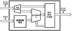
图1示意性示出了本公开实施例的用于深度学习的可重构处理单元的结构框图;FIG. 1 schematically shows a structural block diagram of a reconfigurable processing unit for deep learning according to an embodiment of the present disclosure;
图2示意性示出了本公开实施例的配置控制单元的结构框图;FIG. 2 schematically shows a structural block diagram of a configuration control unit according to an embodiment of the present disclosure;
图3示意性示出了根据本公开实施例的可重构计算在卷积模式下的硬件的微架构图;3 schematically shows a micro-architecture diagram of hardware for reconfigurable computing in convolution mode according to an embodiment of the present disclosure;
图4示意性示出了根据本公开的实施例的可重构计算在池化模式下的硬件的微架构图。FIG. 4 schematically shows a micro-architecture diagram of hardware for reconfigurable computing in a pooling mode according to an embodiment of the present disclosure.
具体实施方式Detailed ways
以下,将参照附图来描述本公开的实施例。但是应该理解,这些描述只是示例性的,而并非要限制本公开的范围。在下面的详细描述中,为便于解释,阐述了许多具体的细节以提供对本公开实施例的全面理解。然而,明显地,一个或多个实施例在没有这些具体细节的情况下也可以被实施。此外,在以下说明中,省略了对公知结构和技术的描述,以避免不必要地混淆本公开的概念。Hereinafter, embodiments of the present disclosure will be described with reference to the accompanying drawings. It should be understood, however, that these descriptions are exemplary only, and are not intended to limit the scope of the present disclosure. In the following detailed description, for convenience of explanation, numerous specific details are set forth in order to provide a thorough understanding of the embodiments of the present disclosure. It will be apparent, however, that one or more embodiments may be practiced without these specific details. Also, in the following description, descriptions of well-known structures and techniques are omitted to avoid unnecessarily obscuring the concepts of the present disclosure.
在此使用的术语仅仅是为了描述具体实施例,而并非意在限制本公开。在此使用的术语“包括”、“包含”等表明了所述特征、步骤、操作和/或部件的存在,但是并不排除存在或添加一个或多个其他特征、步骤、操作或部件。The terminology used herein is for the purpose of describing particular embodiments only and is not intended to limit the present disclosure. The terms "comprising", "comprising" and the like as used herein indicate the presence of stated features, steps, operations and/or components, but do not preclude the presence or addition of one or more other features, steps, operations or components.
在此使用的所有术语(包括技术和科学术语)具有本领域技术人员通常所理解的含义,除非另外定义。应注意,这里使用的术语应解释为具有与本说明书的上下文相一致的含义,而不应以理想化或过于刻板的方式来解释。All terms (including technical and scientific terms) used herein have the meaning as commonly understood by one of ordinary skill in the art, unless otherwise defined. It should be noted that terms used herein should be construed to have meanings consistent with the context of the present specification and should not be construed in an idealized or overly rigid manner.
在使用类似于“A、B和C等中至少一个”这样的表述的情况下,一般来说应该按照本领域技术人员通常理解该表述的含义来予以解释(例如,“具有A、B和C中至少一个的系统”应包括但不限于单独具有A、单独具有B、单独具有C、具有A和B、具有A和C、具有B和C、和/或具有A、B、C的系统等)。在使用类似于“A、B或C等中至少一个”这样的表述的情况下,一般来说应该按照本领域技术人员通常理解该表述的含义来予以解释(例如,“具有A、B或C中至少一个的系统”应包括但不限于单独具有A、单独具有B、单独具有C、具有A和B、具有A和C、具有B和C、和/或具有A、B、C的系统等)。Where expressions like "at least one of A, B, and C, etc.," are used, they should generally be interpreted in accordance with the meaning of the expression as commonly understood by those skilled in the art (eg, "has A, B, and C") At least one of the "systems" shall include, but not be limited to, systems with A alone, B alone, C alone, A and B, A and C, B and C, and/or A, B, C, etc. ). Where expressions like "at least one of A, B, or C, etc.," are used, they should generally be interpreted in accordance with the meaning of the expression as commonly understood by those skilled in the art (eg, "has A, B, or C, etc." At least one of the "systems" shall include, but not be limited to, systems with A alone, B alone, C alone, A and B, A and C, B and C, and/or A, B, C, etc. ).
在实现本公开构思的过程中,发明人发现相关技术中细粒度可重构器主要以进行比特级运算的查找表(LUT,Look-Up-Table)运算的现场可编程逻辑门阵列(FPGA,FieldProgrammable Gate Array)为代表,FPGA的细粒度属性导致算子抽象层级偏细、所需配置信息多,增加了计算过程中信号传输的延时、降低了运算速度。为了满足运算需求,需要增加处理器数量,这导致增大了芯片面积,细粒度可重构器的配置时间过长、无法满足在一些实时性应用中动态实时性配置的需求。In the process of realizing the concept of the present disclosure, the inventor found that the fine-grained reconfigurable device in the related art is mainly a field programmable logic gate array (FPGA, LUT, Look-Up-Table) operation that performs bit-level operations. FieldProgrammable Gate Array) is represented. The fine-grained properties of FPGA lead to a finer abstraction level of operators and a lot of required configuration information, which increases the delay of signal transmission in the calculation process and reduces the calculation speed. In order to meet the computing requirements, the number of processors needs to be increased, which leads to an increase in the chip area, and the configuration time of the fine-grained reconfigurable device is too long, which cannot meet the needs of dynamic real-time configuration in some real-time applications.
为了至少部分地解决相关技术中存在的技术问题,本公开的实施例提供了一种用于深度学习的可重构处理单元。In order to at least partially solve the technical problems existing in the related art, embodiments of the present disclosure provide a reconfigurable processing unit for deep learning.
图1示意性示出了根据本公开实施例的用于深度学习的可重构处理单元的结构框图。FIG. 1 schematically shows a structural block diagram of a reconfigurable processing unit for deep learning according to an embodiment of the present disclosure.
如图1所示,上述用于深度学习的可重构处理单元包括:As shown in Figure 1, the above-mentioned reconfigurable processing unit for deep learning includes:
配置控制单元,用于接收来自外部总线的配置信息和总线命令,并根据上述配置信息和总线命令生成模式指令和控制指令,以及得到配置参数。The configuration control unit is configured to receive configuration information and bus commands from the external bus, and generate mode instructions and control instructions according to the above configuration information and bus commands, and obtain configuration parameters.
先入先出存储器,用于根据上述控制指令,接收外部数据和输出计算结果数据。The first-in-first-out memory is used for receiving external data and outputting calculation result data according to the above control instructions.
多路选择器,用于根据上述模式指令和控制指令,将上述外部数据输入到算术逻辑单元或静态随机存储器。The multiplexer is used for inputting the above-mentioned external data to the arithmetic logic unit or the static random access memory according to the above-mentioned mode instruction and control instruction.
算术逻辑单元,响应于上述控制信息,利用上述配置参数,对来自多路选择器或静态随机存储器的上述外部数据进行计算,得到8比特数据精度或16比特数据精度的计算结果数据,并将计算结果数据输入到上述静态随机存储器或上述先入先出存储器。The arithmetic logic unit, in response to the above-mentioned control information, uses the above-mentioned configuration parameters to calculate the above-mentioned external data from the multiplexer or the static random access memory to obtain the calculation result data of 8-bit data precision or 16-bit data precision, and calculate The resulting data is input to the above-mentioned static random access memory or the above-mentioned first-in-first-out memory.
静态随机存储器,响应于上述模式指令和控制指令,用于存储来自上述算术逻辑单元产生的计算结果数据或上述外部数据,将上述计算结果数据或外部数据输出到上述算术逻辑单元,或将上述计算结果数据输出到上述先入先出存储器。The static random access memory, in response to the above-mentioned mode instruction and control instruction, is used to store the calculation result data or the above-mentioned external data generated from the above-mentioned arithmetic logic unit, and output the above-mentioned calculation result data or external data to the above-mentioned arithmetic logic unit, or the above-mentioned calculation The resulting data is output to the above-mentioned FIFO memory.
根据本公开实施例,配置控制单元,配置参数可以输入到算术逻辑单元中与外部数据进行计算,通过控制配置参数可以调整计算结果数据的精度,满足不同计算精度要求。According to the embodiment of the present disclosure, the control unit is configured, the configuration parameters can be input into the arithmetic logic unit to perform calculations with external data, and the accuracy of the calculation result data can be adjusted by controlling the configuration parameters to meet different calculation accuracy requirements.
图2示意性示出了根据本公开实施例的配置控制单元的结构框图。FIG. 2 schematically shows a structural block diagram of a configuration control unit according to an embodiment of the present disclosure.
如图2所示,上述配置控制单元包括:As shown in Figure 2, the above configuration control unit includes:
配置寄存器,用于接收来自外部总线的配置信息,生成上述模式指令;以及,控制器,用于接收来自外部总线的总线命令,生成上述使能信号;上述配置寄存器还用于根据来自上述控制器的使能信号,基于配置信息得到上述配置参数;以及,上述控制器还用于根据响应于上述模式指令,基于配置信息得到上述控制指令。The configuration register is used to receive the configuration information from the external bus and generate the above-mentioned mode command; and the controller is further configured to obtain the control instruction based on the configuration information in response to the mode instruction.
根据本公开实施例,配置控制单元接收外部总线的配置信息和总线命令,得到模式指令和控制指令并发送给静态随机存储器、多路选择、算术逻辑单元、先入先出存储器,通过配置控制单元指定可重构处理单元的功能、控制可重构处理单元的计算流程。According to the embodiment of the present disclosure, the configuration control unit receives the configuration information and bus commands of the external bus, obtains the mode command and the control command, and sends them to the static random access memory, multiplexing, arithmetic logic unit, and first-in-first-out memory, specified by the configuration control unit The function of the reconfigurable processing unit, and the calculation flow of the control of the reconfigurable processing unit.
根据本公开的实施例,上述配置寄存器可以包括:单元模式寄存器、行寄存器、列寄存器、池化模式寄存器、通道寄存器、量化寄存器。According to an embodiment of the present disclosure, the above-mentioned configuration registers may include: a unit mode register, a row register, a column register, a pooling mode register, a channel register, and a quantization register.
上述单元模式寄存器接收来自外部总线的配置信息,根据上述配置信息生成模式指令,上述模式指令包含卷积模式指令和池化模式指令;以及,在上述单元模式寄存器生成上述卷积模式指令的情况下,上述行寄存器、列寄存器、通道寄存器、量化寄存器响应于来自上述控制器的使能信号,基于上述配置信息生成上述配置参数;在上述单元模式寄存器生成上述池化模式指令的情况下,上述行寄存器、列寄存器、池化模式寄存器响应于来自上述控制器的使能信号,基于上述配置信息生成上述配置参数。The above-mentioned unit mode register receives configuration information from an external bus, and generates a mode command according to the above-mentioned configuration information, and the above-mentioned mode command includes a convolution mode command and a pooling mode command; And, in the case that the above-mentioned unit mode register generates the above-mentioned convolution mode command , the above-mentioned row register, column register, channel register, and quantization register generate the above-mentioned configuration parameters based on the above-mentioned configuration information in response to an enable signal from the above-mentioned controller; in the case where the above-mentioned unit mode register generates the above-mentioned pooling mode instruction, the above-mentioned row The register, the column register, and the pooling mode register generate the configuration parameter based on the configuration information in response to the enable signal from the controller.
根据本公开实施例,配置寄存器中的通道寄存器可以含有通道累加寄存器(chan_add_reg)和重复累加寄存器(chan_add_re_reg),在通道寄存器生成的配置参数中,高8比特表示重复累加寄存器生成的配置参数,低8比特表示通道累加寄存器生成的配置参数。配置寄存器中的量化寄存器可以包括量化移位寄存器和量化参数寄存器。在量化寄存器生成的配置参数中,量化寄存器响应于控制信号,可以向算术逻辑单元输出一串37比特长度的配置参数,高5比特表示量化移位寄存器生成的配置参数,低32比特表示量化参数寄存器生成的配置参数;量化寄存器生成的配置参数与不同模式指令控制下算术逻辑单元中的计算数据结合,确定计算结果数据的精度,量化移位寄存器表示计算数据需要进行左移的数据位宽。According to an embodiment of the present disclosure, the channel register in the configuration register may contain a channel accumulation register (chan_add_reg) and a repeat accumulation register (chan_add_re_reg). The 8 bits represent the configuration parameters generated by the channel accumulation register. The quantization registers in the configuration register may include a quantization shift register and a quantization parameter register. Among the configuration parameters generated by the quantization register, the quantization register can output a string of configuration parameters with a length of 37 bits to the arithmetic logic unit in response to the control signal. The upper 5 bits represent the configuration parameters generated by the quantization shift register, and the lower 32 bits represent the quantization parameters. The configuration parameters generated by the register; the configuration parameters generated by the quantization register are combined with the calculation data in the arithmetic logic unit under the control of different mode instructions to determine the precision of the calculation result data. The quantization shift register indicates the data bit width that the calculation data needs to be shifted to the left.
配置寄存器根据来自外部总线的配置信息,使其中不同寄存器产生配置参数,可以基于配置参数确定计算数据的行信息、列信息、指定不同寄存器的功能。实现只通过外部总线对可重构处理单元进行单次配置,控制可重构处理单元进行多次计算的功能。如果要改变配置寄存器的配置参数,可以通过外部总线重新输入配置信号,实现不同模式计算的实时切换。The configuration register enables different registers to generate configuration parameters according to the configuration information from the external bus, and can determine the row information and column information of the calculation data and the function of specifying different registers based on the configuration parameters. The function of configuring the reconfigurable processing unit only once through the external bus and controlling the reconfigurable processing unit to perform multiple calculations is realized. If you want to change the configuration parameters of the configuration register, you can re-input the configuration signal through the external bus to realize real-time switching between different modes of calculation.
根据本公开的实施例,上述控制器包括:译码器、累加状态机、发送状态机、加载状态机、最大值状态机、输出状态机。According to an embodiment of the present disclosure, the above-mentioned controller includes: a decoder, an accumulation state machine, a transmission state machine, a loading state machine, a maximum value state machine, and an output state machine.
其中,上述累加状态机、发送状态机用于响应于上述卷积模式指令接收来自外部总线的总线命令,生成上述使能信号,以及基于译码器译码的上述配置信息得到上述控制指令;上述加载状态机、最大值状态机、输出状态机用于响应于上述池化模式指令,接收来自外部总线的总线命令,生成上述使能信号,以及基于译码器译码的上述配置信息得到上述控制指令。Wherein, the above-mentioned accumulating state machine and transmitting state machine are used to receive the bus command from the external bus in response to the above-mentioned convolution mode instruction, generate the above-mentioned enable signal, and obtain the above-mentioned control instruction based on the above-mentioned configuration information decoded by the decoder; the above-mentioned The loading state machine, the maximum value state machine, and the output state machine are used to receive the bus command from the external bus in response to the above-mentioned pooling mode command, generate the above-mentioned enable signal, and obtain the above-mentioned control based on the above-mentioned configuration information decoded by the decoder instruction.
根据本公开实施例,控制器中的累加状态机(Cadd_state)和发送状态机(Send_state)响应于上述卷积模式,共同控制多路选择器、算术逻辑单元、静态随机存储器;累加状态机控制先入先出存储器接收外部数据,发送状态机先入先出存储器输出计算结果数据。According to the embodiment of the present disclosure, the accumulating state machine (Cadd_state) and the sending state machine (Send_state) in the controller jointly control the multiplexer, the arithmetic logic unit, and the static random access memory in response to the above-mentioned convolution mode; the accumulating state machine controls the first-in The first-in-first-out memory receives external data, and the sending state machine outputs the calculation result data in the first-in-first-out memory.
控制器中的累加状态机(Cadd_state)表示通过接收外部数据完成乘累加操作,得到部分和数据,并将部分和数据存入静态随机存储器中,如果累加状态机控制的下没有完成所有部分和数据计算,则需要通过取出静态随机存储器中的多个部分和数据重新累加,完成数据计算。The accumulating state machine (Cadd_state) in the controller indicates that the multiply-accumulate operation is completed by receiving external data, and the partial sum data is obtained, and the partial sum data is stored in the static random access memory. If all parts and data are not completed under the control of the accumulating state machine For calculation, it is necessary to complete the data calculation by taking out multiple parts in the static random access memory and accumulating the data again.
根据本公开实施例,控制器中的加载状态机、最大值状态机、输出状态机响应于上述池化模式指令共同控制多路选择器、算术逻辑单元、静态随机存储器;加载状态机控制先入先出存储器接收外部数据,输出状态机先入先出存储器输出计算结果数据。According to the embodiment of the present disclosure, the load state machine, the maximum value state machine, and the output state machine in the controller jointly control the multiplexer, the arithmetic logic unit, and the static random access memory in response to the above-mentioned pooling mode instruction; The output memory receives external data, and the output state machine first-in-first-out memory outputs the calculation result data.
根据本公开的实施例,上述配置控制单元用于:According to an embodiment of the present disclosure, the above configuration control unit is used to:
确定上述先入先出存储器的状态;在确定上述先入先出存储器处于空状态情况下,上述先入先出存储器不向上述多路选择器输出外部数据,使得上述可重构处理单元不进行计算;以及在确定上述先入先出存储器处于满状态情况下,上述先入先出存储器不获取上述可重构处理单元产生的计算结果数据,使得上述可重构处理单元不进行计算。Determine the state of the above-mentioned FIFO memory; when it is determined that the above-mentioned FIFO memory is in an empty state, the above-mentioned FIFO memory does not output external data to the above-mentioned multiplexer, so that the above-mentioned reconfigurable processing unit does not perform calculation; And When it is determined that the FIFO memory is in a full state, the FIFO memory does not acquire the calculation result data generated by the reconfigurable processing unit, so that the reconfigurable processing unit does not perform calculation.
在上述先入先出存储器不处于空状态或满状态情况下,上述先入先出存储器向上述多路选择器输出外部数据,以及向上述可重构处理单元外部输出计算结果数据,使得上述可重构处理单元开始进行计算。When the above-mentioned FIFO memory is not in an empty state or a full state, the above-mentioned FIFO memory outputs external data to the above-mentioned multiplexer, and outputs calculation result data to the above-mentioned reconfigurable processing unit outside, so that the above-mentioned reconfigurable The processing unit begins to perform calculations.
根据本公开实施例,先由配置控制单元根据来自外部总线的配置信息和总线命令对上述可重构处理单元进行配置,后由先入先出存储器根据控制指令执行对数据的接收和输出,实现数据控制,使可重构处理单元在计算开始前先配置模块内部子单元状态,配置完成之后再接收外部数据执行特定操作。可重构处理单元模块内部各个子单元的相对独立,只需要配置控制单元分别进行控制,而不需要在计算过程中对重构处理单元模块内部各个子单元联合控制,减少了外部总线的配置信息和总线命令的数据量。According to the embodiment of the present disclosure, the above-mentioned reconfigurable processing unit is first configured by the configuration control unit according to the configuration information and bus commands from the external bus, and then the FIFO memory performs data reception and output according to the control commands to realize the data Control, so that the reconfigurable processing unit configures the state of the internal subunits of the module before the calculation starts, and then receives external data to perform specific operations after the configuration is completed. Each sub-unit inside the reconfigurable processing unit module is relatively independent, only the control unit needs to be configured to control separately, and it is not necessary to jointly control each sub-unit inside the reconfigurable processing unit module during the calculation process, which reduces the configuration information of the external bus and the data volume of the bus command.
根据本公开的实施例,上述多路选择器用于:According to an embodiment of the present disclosure, the above-mentioned multiplexer is used to:
上述多路选择器响应于上述控制指令和卷积模式指令,将上述先入先出存储器接收的第一输入队列的上述外部数据输入上述算术逻辑单元或上述静态随机存储器;The above-mentioned multiplexer, in response to the above-mentioned control instruction and the convolution mode instruction, inputs the above-mentioned external data of the first input queue received by the above-mentioned FIFO memory into the above-mentioned arithmetic logic unit or the above-mentioned static random access memory;
上述多路选择器响应于上述控制指令和池化模式指令,将上述先入先出存储器接收的第二输入队列的上述外部数据输入上述算术逻辑单元或上述静态随机存储器。In response to the control instruction and the pooling mode instruction, the multiplexer inputs the external data of the second input queue received by the FIFO memory into the arithmetic logic unit or the static random access memory.
根据本公开实施例,使用一个多路选择器响应于上述控制指令和不同的模式指令,可以实现在一个可重构处理单元中只使用一个多路选择器对来自先入先出存储器接收的外部数据的来源进行选择,并将外部数据输入算术逻辑单元或静态随机存储器,减少了多路选择器的使用数量,减小可重构处理单元的体积,提高硬件资源利用率。According to the embodiment of the present disclosure, using one multiplexer in response to the above-mentioned control instructions and different mode instructions can realize that only one multiplexer is used in a reconfigurable processing unit for external data received from the FIFO memory. The source of the selection, and input the external data into the arithmetic logic unit or the static random access memory, which reduces the number of multiplexers used, reduces the size of the reconfigurable processing unit, and improves the utilization of hardware resources.
根据本公开的实施例,上述算术逻辑单元包括:加法器、乘法器、移位器、输出图计数器、通道计数器、部分和寄存器。According to an embodiment of the present disclosure, the above-mentioned arithmetic logic unit includes: an adder, a multiplier, a shifter, an output map counter, a channel counter, a section, and a register.
上述卷积模式指令包含乘法指令和加法指令。The above convolution mode instructions include multiply instructions and add instructions.
上述控制器响应于上述卷积模式指令,上述累加状态机、发送状态机基于译码器译码上述配置信息,得到上述控制指令。The controller responds to the convolution mode command, and the accumulation state machine and the sending state machine decode the configuration information based on a decoder to obtain the control command.
上述先入先出存储器响应于上述卷积模式指令和上述累加状态机、发送状态机生成的上述控制指令,接收外部数据和输出计算结果数据。The above-mentioned FIFO memory receives external data and outputs calculation result data in response to the above-mentioned convolution mode command, the above-mentioned accumulation state machine, and the above-mentioned control command generated by the sending state machine.
上述多路选择器响应于上述卷积模式指令和上述累加状态机生成的上述控制指令,将上述先入先出存储器接收的第一输入队列的上述外部数据输入上述算术逻辑单元。The multiplexer inputs the external data of the first input queue received by the FIFO memory into the arithmetic logic unit in response to the convolution mode command and the control command generated by the accumulation state machine.
上述算术逻辑单元的上述输出图计数器响应于上述累加状态机生成的上述控制指令,确定算术逻辑单元计算后的输出图的行数和列数,控制输出图的大小。The output map counter of the arithmetic logic unit determines the number of rows and columns of the output map calculated by the arithmetic logic unit in response to the control instruction generated by the accumulation state machine, and controls the size of the output map.
上述算术逻辑单元的上述通道计数器响应于上述发送状态机生成的上述控制指令,确定计算时通道累加的次数、计算时数据存取静态随机存储器的次数。The channel counter of the arithmetic logic unit, in response to the control instruction generated by the sending state machine, determines the number of times of channel accumulation and the number of times of data access to the static random access memory during calculation.
上述算术逻辑单元上述加法器、乘法器、移位器、部分和寄存器利用上述计算时通道累加的次数、计算时数据存取静态随机存储器的次数对上述外部数据进行计算,实现对上述外部数据的向量乘法、矩阵乘法、矩阵加法运算,得到计算结果数据。以及Above-mentioned arithmetic logic unit above-mentioned adder, multiplier, shifter, part and register utilize the number of times of channel accumulation during the above-mentioned calculation and the number of times of data access static random access memory during the calculation to calculate the above-mentioned external data, and realize the above-mentioned external data. Vector multiplication, matrix multiplication, and matrix addition operations to obtain calculation result data. as well as
响应于上述卷积模式指令,上述控制器将上述量化寄存器的上述上述配置参数译码,译码后的配置参数通过上述乘法器与上述计算结果数据相乘,得到8比特数据精度或16比特数据精度的计算结果数据。In response to the above-mentioned convolution mode instruction, the above-mentioned controller decodes the above-mentioned configuration parameters of the above-mentioned quantization register, and the decoded configuration parameters are multiplied by the above-mentioned calculation result data by the above-mentioned multiplier to obtain 8-bit data precision or 16-bit data. Accuracy calculation result data.
图3示意性示出了根据本公开实施例的可重构计算在卷积模式下的硬件的微架构图。FIG. 3 schematically shows a micro-architecture diagram of hardware for reconfigurable computing in a convolution mode according to an embodiment of the present disclosure.
图3中虚线表示可重构处理单元中的控制信号,实线部分表示可重构处理单元中的数据信号;先入先出存储器空状态或满状态情况下产生的的空信号满信号不需要在图中反映;模式配置、配置使能、通道配置和量化配置均为配置控制单元相应的配置信号和使能信号。The dotted line in Fig. 3 represents the control signal in the reconfigurable processing unit, and the solid line part represents the data signal in the reconfigurable processing unit; the empty signal and the full signal generated in the FIFO memory empty state or full state do not need to be It is reflected in the figure; mode configuration, configuration enable, channel configuration and quantization configuration are the corresponding configuration signals and enable signals of the configuration control unit.
如图3所示,单元模式寄存器接收来自外部总线的配置信息,被设置为具体的卷积模式指令。累加状态机、发送状态机基于具体的卷积模式指令,生成对应使能信号。行寄存器、列寄存器、通道寄存器、量化寄存器响应于对应使能信号,基于接收到来自外部总线的配置信息生成配置参数。译码器基于配置参数译码生成控制信号,并将控制信号输入算术逻辑单元。控制信号可以包括累加状态机生成的有关行寄存器、列寄存器的控制信号,发送状态机生成的控制信号,以及有关通道寄存器、量化寄存器的控制信号。As shown in Figure 3, the unit mode register receives configuration information from the external bus and is set as a specific convolution mode command. The accumulation state machine and the sending state machine generate corresponding enable signals based on specific convolution mode instructions. The row registers, column registers, channel registers, and quantization registers generate configuration parameters based on the configuration information received from the external bus in response to the corresponding enable signals. The decoder decodes and generates a control signal based on the configuration parameters, and inputs the control signal to the arithmetic logic unit. The control signals may include control signals related to row registers and column registers generated by the accumulation state machine, control signals generated by the transmit state machine, and control signals related to channel registers and quantization registers.
先入先出存储器响应于累加状态机的接收请求,接收外部数据。外部数据可以包括第一输入队列的外部数据和第二输入队列的外部数据。先入先出存储器响应于发送状态机的发送请求,输出计算结果数据。多路选择器响应于控制指令和具体的卷积模式指令,接收来自先入先出存储器的第一输入队列的外部数据,并将外部数据输入算术逻辑单元。The first-in-first-out memory receives external data in response to a receive request from the accumulation state machine. The external data may include external data of the first input queue and external data of the second input queue. The first-in-first-out memory outputs calculation result data in response to a transmission request of the transmission state machine. The multiplexer receives external data from the first input queue of the FIFO memory and inputs the external data into the arithmetic logic unit in response to the control command and the specific convolution mode command.
算术逻辑单元可以包括输出图计数器和部分和寄存器。输出图计数器输出图计数器响应于累加状态机发送的有关行寄存器、列寄存器的控制信号,控制输出图的大小。部分和寄存器响应于发送状态机发送的控制信号,进行部分和数据的暂存。算术逻辑单元响应于有关通道寄存器、量化寄存器的控制信号,对数据进行乘累加和数据位宽的处理。此外,算术逻辑单元还可以包括加法器、乘法器、激活单元和移位寄存器、通道计数器。算术逻辑单元可以主要用于实现乘法、加法、乘累加、移位、比较等操作。The arithmetic logic unit may include output graph counters and partial sum registers. Output map counter The output map counter controls the size of the output map in response to control signals sent by the accumulation state machine about the row register and the column register. The partial sum register performs temporary storage of the partial sum data in response to the control signal sent by the sending state machine. The arithmetic logic unit performs multiplication and accumulation and data bit width processing on the data in response to the control signals related to the channel register and the quantization register. In addition, the arithmetic logic unit may also include adders, multipliers, activation units and shift registers, channel counters. The arithmetic logic unit can be mainly used to implement operations such as multiplication, addition, multiply-accumulate, shift, and comparison.
根据本公开实施例,卷积模式主要实现的功能为向量乘法功能和矩阵加法功能,其中具体配置信息表示为如下表1:According to the embodiment of the present disclosure, the functions mainly implemented by the convolution mode are the vector multiplication function and the matrix addition function, and the specific configuration information is represented as the following Table 1:
表1Table 1

向量乘加功能:对于现有的卷积神经网络,通常卷积核大小为3×3,可将卷积核展开为长度为9的一维向量运算。Vector multiply-add function: For the existing convolutional neural network, the size of the convolution kernel is usually 3×3, and the convolution kernel can be expanded into a one-dimensional vector operation with a length of 9.
如上图表1中功能“1”所示,设置spe_mode=“vect_mac”模式,row_reg=“1”,col_reg=“1”,chan_add_reg=“9”,chan_add_re_reg=“1”完成9×1的向量累加运算并且将计算结果输出到可重构单元之外。单元模式(spe_mode)参数寄存器设置算术逻辑单元的功能为乘累加操作,并且将乘累加结果放置到内部的部分和(Psum)寄存器中。算术逻辑单元中乘累加单元由加法器和乘法器以二阶流水线的设计方式得到,可以减少关键路径的延迟。乘累加单元只针对8比特的输入数据进行处理,对应设置部分和寄存器的位宽为32比特,保证部分和数据的输出结果不会溢出,计算完成的结果通过乘以比例因子的方法进行截位处理,保证输出结果的精度。重复累加寄存器(chan_add_re_reg)=1,表示进行向量计算的结果直接输出到输出先入先出存储器中。As shown in the function "1" in Figure 1 above, set spe_mode="vect_mac" mode, row_reg="1", col_reg="1", chan_add_reg="9", chan_add_re_reg="1" to complete the 9×1 vector accumulation operation And output the calculation result outside the reconfigurable unit. The unit mode (spe_mode) parameter register sets the function of the arithmetic logic unit as multiply-accumulate operation, and places the multiply-accumulate result into the internal partial sum (Psum) register. The multiply-accumulate unit in the arithmetic logic unit is obtained by the adder and the multiplier in the design of the second-order pipeline, which can reduce the delay of the critical path. The multiply-accumulate unit only processes 8-bit input data, and the bit width of the corresponding setting part and register is 32 bits to ensure that the output result of the part and data will not overflow, and the calculated result is truncated by multiplying the scale factor. processing to ensure the accuracy of the output results. Repeat accumulation register (chan_add_re_reg)=1, indicating that the result of vector calculation is directly output to the output FIFO memory.
如上图表1中功能“2”所示,设置spe_mode=“vect_mac”模式,row_reg=“2”,col_reg=“2”,chan_add_reg=“9”,chan_add_re_reg=“2”,完成行数和列数分别为2×2的卷积核,且卷积核大小为9,输入通道是2的卷积运算。首先将第一个通道的计算结果存入到静态随机存储器中,然后计算第二通道的结果,并且将第二个通道的计算机结果和第一个通达的计算结果进行累加完成两个通道的乘累加计算。As shown in function "2" in Figure 1 above, set spe_mode="vect_mac" mode, row_reg="2", col_reg="2", chan_add_reg="9", chan_add_re_reg="2", complete the number of rows and columns respectively It is a 2×2 convolution kernel, and the convolution kernel size is 9, and the input channel is a convolution operation of 2. First, the calculation result of the first channel is stored in the static random access memory, then the result of the second channel is calculated, and the computer result of the second channel and the calculation result of the first channel are accumulated to complete the multiplication of the two channels. cumulative calculation.
矩阵累加功能:可重构处理单元支持流模式操作,具体的,通过先入先出存储器获取一个矩阵,可重构处理单元将矩阵存储到静态随机存储器中,然后等待下一次配置控制单元输入第二矩阵,此时从静态随机存储器中取出第一矩阵和第二矩阵累加,如果chan_add_re_reg=“1”则直接输出到先入先出存储器,如果chan_add_re_reg设置为n,则等待n个大小相同的矩阵输入完成之后,将输出结果送到输出先入先出存储器中。Matrix accumulation function: The reconfigurable processing unit supports stream mode operation. Specifically, a matrix is obtained through the first-in-first-out memory, the reconfigurable processing unit stores the matrix in the static random access memory, and then waits for the next configuration control unit to input the second Matrix, at this time, the first matrix and the second matrix are taken out from the static random access memory and accumulated. If chan_add_re_reg=“1”, it is directly output to the first-in-first-out memory. If chan_add_re_reg is set to n, wait for the input of n matrices of the same size to complete. After that, the output result is sent to the output FIFO memory.
完成所有输入通道和卷积核的乘累加操作之后,需要对输出图进行量化。为了满足不同深度学习算法需要的精度不同,通过可以加载外部输入的量化参数到量化参数寄存器,将输出数据乘以输入的量化参数并且截取指定位宽来对于输出图数据进行不同精度要求的量化。After completing the multiply-accumulate operations of all input channels and convolution kernels, the output map needs to be quantized. In order to meet the different precisions required by different deep learning algorithms, the output image data can be quantized with different precision requirements by loading the externally input quantization parameters into the quantization parameter register, multiplying the output data by the input quantization parameters and intercepting the specified bit width.
根据本公开的实施例,上述算术逻辑单元还包括最大值寄存器、最大值计数器、比较器。According to an embodiment of the present disclosure, the above-mentioned arithmetic logic unit further includes a maximum value register, a maximum value counter, and a comparator.
上述池化模式指令包含最大池化指令、平均池化指令。The above pooling mode commands include maximum pooling commands and average pooling commands.
上述控制器响应于上述池化模式指令,上述加载状态机、最大值状态机、输出状态机基于译码器译码上述配置信息,得到上述控制指令。The controller responds to the pooling mode command, and the load state machine, the maximum value state machine, and the output state machine decode the configuration information based on a decoder to obtain the control command.
上述先入先出存储器响应于上述池化模式指令和上述加载状态机、输出状态机生成的上述控制指令,接收外部数据和输出计算结果数据。The FIFO memory receives external data and outputs calculation result data in response to the pooling mode command and the control command generated by the load state machine and the output state machine.
上述多路选择器上述卷积模式指令和上述累加状态机生成的上述控制指令,将上述先入先出存储器接收的第二输入队列的上述外部数据输入上述算术逻辑单元。The convolution mode command of the multiplexer and the control command generated by the accumulation state machine input the external data of the second input queue received by the FIFO memory into the arithmetic logic unit.
上述算术逻辑单元的上述输出图计数器响应于上述加载状态机生成的上述控制指令,确定算术逻辑单元计算后的输出图的行数和列数,控制输出图的大小。The output graph counter of the arithmetic logic unit determines the number of rows and columns of the output graph calculated by the arithmetic logic unit in response to the control instruction generated by the loading state machine, and controls the size of the output graph.
上述算术逻辑单元的上述最大值寄存器响应于上述最大值状态机生成的上述控制指令,用于存储每个通道计算时最大池化核的最大值。The above-mentioned maximum value register of the above-mentioned arithmetic logic unit is used to store the maximum value of the maximum pooling kernel in the calculation of each channel in response to the above-mentioned control instruction generated by the above-mentioned maximum value state machine.
上述算术逻辑单元的上述最大值寄存器、最大值计数器、部分和寄存器、比较器、加法器、输出图计数器利用上述外部数据进行计算,实现对上述外部数据的最大池化、平均池化运算,得到计算结果数据。The above-mentioned maximum value register, maximum value counter, partial sum register, comparator, adder, and output graph counter of the above-mentioned arithmetic logic unit are calculated by using the above-mentioned external data, so as to realize the maximum pooling and average pooling operations on the above-mentioned external data, and obtain Calculate the resulting data.
图4示意性示出了根据本公开的实施例的可重构计算在池化模式下的硬件的微架构图。FIG. 4 schematically shows a micro-architecture diagram of hardware for reconfigurable computing in a pooling mode according to an embodiment of the present disclosure.
图4中虚线、实线先入先出存储器产生的的空信号满信号设置与图3相同,在此不再赘述。In FIG. 4 , the setting of the empty signal and the full signal generated by the FIFO memory with the dotted line and the solid line is the same as that in FIG. 3 , and will not be repeated here.
如图4所示,单元模式寄存器接收来自外部总线的配置信息,被设置为具体的卷积模式指令。加载状态机、最大值状态机、输出状态机基于具体的卷积模式指令生成对应使能信号。行寄存器、列寄存器、池化模式寄存器响应于对应使能信号,基于接收到来自外部总线的配置信息配置信息生成配置参数。译码器基于配置参数译码生成控制信号,并将控制信号输入算术逻辑单元。控制信号可以包括加载状态机发送的有关行寄存器、列寄存器的控制信号,以及加载状态机发送的有关池化模式寄存器的控制信号。As shown in Figure 4, the unit mode register receives configuration information from the external bus and is set as a specific convolution mode command. The load state machine, the maximum value state machine, and the output state machine generate corresponding enable signals based on specific convolution mode instructions. The row register, the column register, and the pooling mode register generate configuration parameters based on the configuration information received from the external bus in response to the corresponding enable signal. The decoder decodes and generates a control signal based on the configuration parameters, and inputs the control signal to the arithmetic logic unit. The control signals may include control signals sent by the load state machine regarding row registers, column registers, and control signals sent by the load state machine regarding pooling mode registers.
先入先出存储器响应于加载状态机的接收请求,接收外部数据。先入先出存储器响应于输出状态机的发送请求,输出计算结果数据。多路选择器响应于控制指令和卷积模式指令,接收自先入先出存储器的的第二输入队列的外部数据,并将外部数据输入算术逻辑单元。The first-in-first-out memory receives external data in response to a receive request to load the state machine. The first-in-first-out memory outputs calculation result data in response to a send request from the output state machine. The multiplexer receives external data from the second input queue of the FIFO memory and inputs the external data to the arithmetic logic unit in response to the control instruction and the convolution mode instruction.
算术逻辑单元中输出图计数器响应于加载状态机发送的有关行寄存器、列寄存器的控制信号,控制输出图的大小。最大值寄存器响应于加载状态机发送的有关池化模式寄存器的控制信号,控制算术逻辑单元进行具体的池化操作。部分和寄存器缓存最大池化、平均池化等操作中产生的数据。算术逻辑单元可以具体展开为加法器、乘法器、比较器、最大值寄存器、最大值计数器、比较器、加法器。算术逻辑单元可以主要实现最大池化、平均池化等操作。The output map counter in the arithmetic logic unit controls the size of the output map in response to the control signals related to the row register and the column register sent by the loading state machine. The maximum value register controls the arithmetic logic unit to perform a specific pooling operation in response to a control signal about the pooling mode register sent by the loading state machine. Partial and register caches of data resulting from operations such as max pooling, average pooling, etc. The arithmetic logic unit can be specifically expanded into an adder, a multiplier, a comparator, a maximum value register, a maximum value counter, a comparator, and an adder. The arithmetic logic unit can mainly implement operations such as maximum pooling and average pooling.
根据本公开实施例,通过复用静态随机存储器和对应算术逻辑单元完成不同要求的池化操作:如:池化核为2或池化核为3的步长可变的池化运算。当完成池化核为7的平均池化运算,通过量化寄存器中缓存的量化因子,完成除法单元的计算,避免使用除法器,减小可重构处理单元体积。According to the embodiments of the present disclosure, pooling operations with different requirements are accomplished by multiplexing the SRAM and the corresponding arithmetic logic unit: for example, a pooling operation with a pooling kernel of 2 or a pooling kernel of 3 with a variable step size. When the average pooling operation with a pooling core of 7 is completed, the calculation of the division unit is completed by the quantization factor cached in the quantization register, avoiding the use of a divider and reducing the volume of the reconfigurable processing unit.
更具体的,可以设置spe_mode=“max_pool”模式,设置算术逻辑单元执行比较器功能,每次开始最大池化计算前,将输入图通过多路选择器加载到静态随机存储器中,虽然相比于专用的池化电路增加了存入数据的周期,但“max_pool”模式保证输入图可以在完成卷积之后可以直接进行池化,同时可以完成不同滑动步长和不同卷积核的池化。More specifically, you can set spe_mode="max_pool" mode, set the arithmetic logic unit to perform the comparator function, and load the input map into the static random access memory through the multiplexer before each start of the maximum pooling calculation, although compared to The dedicated pooling circuit increases the period of storing data, but the "max_pool" mode ensures that the input image can be directly pooled after the convolution is completed, and the pooling of different sliding steps and different convolution kernels can be completed at the same time.
可以静态随机存储器设计大小为1024×32,如果输入图是8比特数据,则每次最多可以支持四个通道同时进行池化。每次开始时将第一个数放到最大值寄存器(max_reg)中,如果最大值池化核(kernel_size)设置为2,则每个窗口的4个数输出一个最大结果放到最大值寄存器中,如果最大值池化核设置为3,则每个窗口9个数输出一个最大结果放到最大值寄存器中。The SRAM can be designed with a size of 1024×32. If the input image is 8-bit data, it can support up to four channels for simultaneous pooling at a time. Put the first number in the maximum register (max_reg) at the beginning of each time. If the maximum pooling kernel (kernel_size) is set to 2, then 4 numbers of each window will output a maximum result and put it in the maximum register. , if the maximum pooling kernel is set to 3, each window will output a maximum result of 9 numbers and put it in the maximum value register.
可以设置spe_mode=“avg_pool”模式,则算术逻辑单元功能调用之前的乘累加单元,完成窗口的部分和的乘累加操作。算术逻辑单元将完成窗口的部分和的乘累加操作得到的数据乘以比例因子,完成平均计算。如果完成7×7的平均池化,则将完成长度为49的向量乘累加计算之后,将49缓存到量化寄存器中作为量化因子,使用时乘以49的倒数,然后通过截位操作,完成除法计算,达到平均池化的计算效果。You can set spe_mode="avg_pool" mode, then the arithmetic logic unit function calls the previous multiply-accumulate unit to complete the multiply-accumulate operation of the partial sum of the window. The arithmetic logic unit multiplies the data obtained by the multiply-accumulate operation of the partial sum of the window by the scale factor to complete the average calculation. If the average pooling of 7×7 is completed, after the multiplication and accumulation calculation of the vector of length 49 is completed, 49 is cached in the quantization register as the quantization factor, multiplied by the reciprocal of 49 when used, and then the division is completed through the truncation operation. Calculate to achieve the calculation effect of average pooling.
根据本公开实施例,可重构处理器可以以8比特数据精度或16比特数据精度的算术逻辑单元和32比特数据精度的存储单元作为最小的重构粒度进行数据计算,数据粒度变大可以减小可重构处理器所需配置信息量,可以通过重构单元之间的互联结构,增加信号传输带宽,在保证运算速度正常的情况下,减小芯片面积。According to the embodiment of the present disclosure, the reconfigurable processor can perform data calculation with an arithmetic logic unit with 8-bit data precision or 16-bit data precision and a storage unit with 32-bit data precision as the minimum reconstruction granularity, and the larger the data granularity, the smaller the data can be. The amount of configuration information required by the small reconfigurable processor can be increased by reconstructing the interconnect structure between the units to increase the signal transmission bandwidth, and reduce the chip area while ensuring the normal operation speed.
更具体的,可重构处理器的算术逻辑单元的加法器和乘法器都可以进行8比特数据精度或16比特数据精度的数据计算,加法器和乘法器通过二阶流水线设计组合得到的乘加器可以进行8比特数据精度的数据计算,静态随机存储器的内存位宽为32比特。可重构处理器计算数据粒度较大,可以降低所需配置信息量,提高可重构处理器运算速度。More specifically, the adders and multipliers of the arithmetic logic unit of the reconfigurable processor can both perform data calculations with 8-bit data precision or 16-bit data precision, and the adders and multipliers are multiplied and added by combining the second-order pipeline design. The processor can perform data calculation with 8-bit data precision, and the memory bit width of the static random access memory is 32 bits. The reconfigurable processor has a large granularity of computing data, which can reduce the amount of required configuration information and improve the computing speed of the reconfigurable processor.
根据本公开的实施例,上述静态随机存储器还用于:响应于控制信息,基于上述查找表对上述8比特数据精度的计算结果数据进行激活函数运算;响应于控制信息,将16比特数据精度的上述计算结果数据以多段多项式拟合的模式存储,基于上述查找表将每一段16比特数据精度的上述计算结果数据进行激活函数运算,得到多个一阶激活函数运算结果。以及According to an embodiment of the present disclosure, the above-mentioned static random access memory is further configured to: in response to the control information, perform an activation function operation on the above-mentioned 8-bit data precision calculation result data based on the above-mentioned look-up table; in response to the control information, to 16-bit data precision The calculation result data is stored in a multi-segment polynomial fitting mode, and each segment of the calculation result data with 16-bit data precision is subjected to activation function operation based on the lookup table to obtain multiple first-order activation function operation results. as well as
上述算术逻辑单元还用于将上述多个一阶激活函数运算结果累加,得到上述计算结果数据的16比特数据精度的激活函数运算结果。The above-mentioned arithmetic logic unit is further configured to accumulate the above-mentioned multiple first-order activation function operation results to obtain an activation function operation result with 16-bit data precision of the above-mentioned calculation result data.
根据本公开实施例,静态随机存储器还可以存储所述算术逻辑单元的计算中间数据,例如存储部分和数据,使用静态随机存储器存储所述算术逻辑单元的计算中间数据一方面可以增加算术逻辑单元对计算中间数据的访问速度,另一方面静态随机存储器存储时会对数据进行量化处理,静态随机存储器将数据输出后降低了数据所需存储空间。According to the embodiment of the present disclosure, the SRAM can also store the calculation intermediate data of the arithmetic logic unit, such as the storage part and data, and using the SRAM to store the calculation intermediate data of the arithmetic logic unit can increase the number of pairs of arithmetic logic units on the one hand. Calculate the access speed of the intermediate data. On the other hand, the SRAM will quantify the data when it is stored, and the SRAM will reduce the storage space required for the data after outputting the data.
根据本公开实施例,在完成上述输入通道的计算之后,网络层还可能进行激活函数的操作,激活函数可以包括,ReLU函数、Sigmoid函数、Tanh函数等。According to the embodiment of the present disclosure, after completing the calculation of the input channel, the network layer may also perform an activation function operation, and the activation function may include a ReLU function, a Sigmoid function, a Tanh function, and the like.
ReLU函数只要和0相比,大于0则输出正值,可以直接使用算术逻辑单元比较器进行计算。常用可重构处理单元设计中,实现Sigmoid函数、Tanh函数一般只用查找表的方式实现。利用静态随机存储器的地址作为索引,将Tanh函数和Sigmoid函数的结果提前加载到静态随机存储器中,完成查找表的配置。对于典型的8比特数据,可以在静态随机存储器中利用8比特的查找表实现结果查找。对于16比特数据,由于静态随机存储器大小限制,设置了查找表和多项式拟合的方式实现结果查询,实现16比特Sigmoid函数、Tanh函数高精度查找,可以将Sigmoid函数设置成多段多项式拟合的模式,利用polyfit函数将多段一阶拟合函数的系数存入查找表中,利用算术逻辑单元中的乘累加功能,实现利用多段线性函数的实现拟合方式。As long as the ReLU function is compared with 0, if it is greater than 0, it will output a positive value, and the arithmetic logic unit comparator can be directly used for calculation. In the design of commonly used reconfigurable processing units, the implementation of the Sigmoid function and the Tanh function is generally implemented only by means of a lookup table. Using the address of the static random access memory as an index, the results of the Tanh function and the Sigmoid function are loaded into the static random access memory in advance to complete the configuration of the lookup table. For typical 8-bit data, the result lookup can be implemented in SRAM using an 8-bit lookup table. For 16-bit data, due to the size limitation of static random access memory, a look-up table and polynomial fitting are set up to query the results, to achieve high-precision search of 16-bit Sigmoid function and Tanh function, and the Sigmoid function can be set to a multi-segment polynomial fitting mode. , using the polyfit function to store the coefficients of the multi-segment first-order fitting function in the look-up table, and using the multiply-accumulate function in the arithmetic logic unit to realize the fitting method using the multi-segment linear function.
根据本公开实施例,由于部分和寄存器可以将数据累加到静态随机存储器中,使得卷积层和池化层可以进行层融合计算,可以设置spe_mode=“conv_pool”模式,可重构单元可以在完成卷积模式之后进行池化,减少对片外存储的访问,提高计算速度。According to the embodiment of the present disclosure, since the partial sum register can accumulate data into the static random access memory, so that the convolutional layer and the pooling layer can perform layer fusion calculation, the spe_mode="conv_pool" mode can be set, and the reconfigurable unit can be completed after the Pooling is performed after the convolution mode to reduce access to off-chip storage and improve computing speed.
根据本公开实施例,设置计算两个16×16的输入图的矩阵乘法、矩阵加法、最大池化核为2×2步长为2的最大池化、计算计算结果数据16个点的Sigmoid函数值,并对设置的计算进行性能评估,其中计算结果表示为如下表2:According to the embodiment of the present disclosure, set the matrix multiplication, matrix addition, the maximum pooling kernel is 2×2, the step size is 2, and the sigmoid function that calculates the calculation result data of 16 points is set. value, and evaluate the performance of the set calculation, where the calculation results are expressed as the following Table 2:
表2Table 2

面积功耗评估(在SMIC 28nm工艺下的性能),在时钟频率为400m的条件下评估了可重构处理单元的资源消耗和功耗表现。其中面积和功耗表现表示为如下表3:Area power evaluation (performance under SMIC 28nm process), the resource consumption and power consumption performance of reconfigurable processing units are evaluated under the condition of clock frequency of 400m. The area and power consumption performance are expressed as the following Table 3:
表3table 3

可重构处理单元可以近似达到ASIC的能效。The reconfigurable processing unit can approximate the energy efficiency of an ASIC.
误差精度评估,在8比特模式和16比特模式下评估了激活函数的性能表现,性能数值表示为如下表4:Error accuracy evaluation, the performance of the activation function is evaluated in 8-bit mode and 16-bit mode, and the performance values are shown in Table 4 below:
表4Table 4

根据本公开实施例,可重构处理单元还可以设置接收来自外部总线的多种配置信息和总线命令,实现不同的计算操作,可重构处理单元功能配置表可以表示为如下表5:According to the embodiment of the present disclosure, the reconfigurable processing unit can also be configured to receive various configuration information and bus commands from an external bus to implement different computing operations. The reconfigurable processing unit function configuration table can be represented as the following Table 5:
表5table 5

附图中的流程图和框图,图示了按照本公开各种实施例的系统、方法和计算机程序产品的可能实现的体系架构、功能和操作。在这点上,流程图或框图中的每个方框可以代表一个模块、程序段、或代码的一部分,上述模块、程序段、或代码的一部分包含一个或多个用于实现规定的逻辑功能的可执行指令。也应当注意,在有些作为替换的实现中,方框中所标注的功能也可以以不同于附图中所标注的顺序发生。例如,两个接连地表示的方框实际上可以基本并行地执行,它们有时也可以按相反的顺序执行,这依所涉及的功能而定。也要注意的是,框图或流程图中的每个方框、以及框图或流程图中的方框的组合,可以用执行规定的功能或操作的专用的基于硬件的系统来实现,或者可以用专用硬件与计算机指令的组合来实现。本领域技术人员可以理解,本公开的各个实施例和/或权利要求中记载的特征可以进行多种组合和/或结合,即使这样的组合或结合没有明确记载于本公开中。特别地,在不脱离本公开精神和教导的情况下,本公开的各个实施例和/或权利要求中记载的特征可以进行多种组合和/或结合。所有这些组合和/或结合均落入本公开的范围。The flowchart and block diagrams in the Figures illustrate the architecture, functionality, and operation of possible implementations of systems, methods and computer program products according to various embodiments of the present disclosure. In this regard, each block in the flowchart or block diagrams may represent a module, segment, or portion of code that contains one or more logical functions for implementing the specified functions executable instructions. It should also be noted that, in some alternative implementations, the functions noted in the blocks may occur out of the order noted in the figures. For example, two blocks shown in succession may, in fact, be executed substantially concurrently, or the blocks may sometimes be executed in the reverse order, depending upon the functionality involved. It is also noted that each block of the block diagrams or flowchart illustrations, and combinations of blocks in the block diagrams or flowchart illustrations, can be implemented in special purpose hardware-based systems that perform the specified functions or operations, or can be implemented using A combination of dedicated hardware and computer instructions is implemented. Those skilled in the art will appreciate that various combinations and/or combinations of features recited in various embodiments and/or claims of the present disclosure are possible, even if such combinations or combinations are not expressly recited in the present disclosure. In particular, various combinations and/or combinations of the features recited in the various embodiments of the present disclosure and/or in the claims may be made without departing from the spirit and teachings of the present disclosure. All such combinations and/or combinations fall within the scope of this disclosure.
以上对本公开的实施例进行了描述。但是,这些实施例仅仅是为了说明的目的,而并非为了限制本公开的范围。尽管在以上分别描述了各实施例,但是这并不意味着各个实施例中的措施不能有利地结合使用。本公开的范围由所附权利要求及其等同物限定。不脱离本公开的范围,本领域技术人员可以做出多种替代和修改,这些替代和修改都应落在本公开的范围之内。Embodiments of the present disclosure have been described above. However, these examples are for illustrative purposes only, and are not intended to limit the scope of the present disclosure. Although the various embodiments are described above separately, this does not mean that the measures in the various embodiments cannot be used in combination to advantage. The scope of the present disclosure is defined by the appended claims and their equivalents. Without departing from the scope of the present disclosure, those skilled in the art can make various substitutions and modifications, and these substitutions and modifications should all fall within the scope of the present disclosure.
Claims (10)
Priority Applications (1)
| Application Number | Priority Date | Filing Date | Title |
|---|---|---|---|
| CN202210483441.6ACN114780481A (en) | 2022-04-29 | 2022-04-29 | Reconfigurable Processing Units for Deep Learning |
Applications Claiming Priority (1)
| Application Number | Priority Date | Filing Date | Title |
|---|---|---|---|
| CN202210483441.6ACN114780481A (en) | 2022-04-29 | 2022-04-29 | Reconfigurable Processing Units for Deep Learning |
Publications (1)
| Publication Number | Publication Date |
|---|---|
| CN114780481Atrue CN114780481A (en) | 2022-07-22 |
Family
ID=82435127
Family Applications (1)
| Application Number | Title | Priority Date | Filing Date |
|---|---|---|---|
| CN202210483441.6APendingCN114780481A (en) | 2022-04-29 | 2022-04-29 | Reconfigurable Processing Units for Deep Learning |
Country Status (1)
| Country | Link |
|---|---|
| CN (1) | CN114780481A (en) |
Cited By (3)
| Publication number | Priority date | Publication date | Assignee | Title |
|---|---|---|---|---|
| CN116090029A (en)* | 2023-01-13 | 2023-05-09 | 无锡沐创集成电路设计有限公司 | Encryption circuit |
| CN117573065A (en)* | 2024-01-17 | 2024-02-20 | 青岛本原微电子有限公司 | Multifunctional shift operation device and operation method for processor |
| CN119576275A (en)* | 2024-11-28 | 2025-03-07 | 北京智芯微电子科技有限公司 | Runtime reconfigurable artificial intelligence chip, processing unit, computing task execution method and electronic device |
Citations (9)
| Publication number | Priority date | Publication date | Assignee | Title |
|---|---|---|---|---|
| CN106775599A (en)* | 2017-01-09 | 2017-05-31 | 南京工业大学 | Multi-computing-unit coarse-grained reconfigurable system and method for recurrent neural network |
| CN106940815A (en)* | 2017-02-13 | 2017-07-11 | 西安交通大学 | A kind of programmable convolutional neural networks Crypto Coprocessor IP Core |
| CN108647780A (en)* | 2018-04-12 | 2018-10-12 | 东南大学 | Restructural pond operation module structure towards neural network and its implementation |
| CN109102065A (en)* | 2018-06-28 | 2018-12-28 | 广东工业大学 | A kind of convolutional neural networks accelerator based on PSoC |
| CN109343826A (en)* | 2018-08-14 | 2019-02-15 | 西安交通大学 | A reconfigurable processor computing unit for deep learning |
| CN110059493A (en)* | 2019-04-10 | 2019-07-26 | 无锡沐创集成电路设计有限公司 | SKINNY-128-128 Encryption Algorithm realization method and system based on coarseness Reconfigurable Computation unit |
| CN110737628A (en)* | 2019-10-17 | 2020-01-31 | 辰芯科技有限公司 | reconfigurable processor and reconfigurable processor system |
| US20200341758A1 (en)* | 2017-12-29 | 2020-10-29 | Nationz Technologies Inc. | Convolutional Neural Network Hardware Acceleration Device, Convolutional Calculation Method, and Storage Medium |
| CN112199119A (en)* | 2020-10-21 | 2021-01-08 | 上海壁仞智能科技有限公司 | Vector operation device |
- 2022
- 2022-04-29CNCN202210483441.6Apatent/CN114780481A/enactivePending
Patent Citations (9)
| Publication number | Priority date | Publication date | Assignee | Title |
|---|---|---|---|---|
| CN106775599A (en)* | 2017-01-09 | 2017-05-31 | 南京工业大学 | Multi-computing-unit coarse-grained reconfigurable system and method for recurrent neural network |
| CN106940815A (en)* | 2017-02-13 | 2017-07-11 | 西安交通大学 | A kind of programmable convolutional neural networks Crypto Coprocessor IP Core |
| US20200341758A1 (en)* | 2017-12-29 | 2020-10-29 | Nationz Technologies Inc. | Convolutional Neural Network Hardware Acceleration Device, Convolutional Calculation Method, and Storage Medium |
| CN108647780A (en)* | 2018-04-12 | 2018-10-12 | 东南大学 | Restructural pond operation module structure towards neural network and its implementation |
| CN109102065A (en)* | 2018-06-28 | 2018-12-28 | 广东工业大学 | A kind of convolutional neural networks accelerator based on PSoC |
| CN109343826A (en)* | 2018-08-14 | 2019-02-15 | 西安交通大学 | A reconfigurable processor computing unit for deep learning |
| CN110059493A (en)* | 2019-04-10 | 2019-07-26 | 无锡沐创集成电路设计有限公司 | SKINNY-128-128 Encryption Algorithm realization method and system based on coarseness Reconfigurable Computation unit |
| CN110737628A (en)* | 2019-10-17 | 2020-01-31 | 辰芯科技有限公司 | reconfigurable processor and reconfigurable processor system |
| CN112199119A (en)* | 2020-10-21 | 2021-01-08 | 上海壁仞智能科技有限公司 | Vector operation device |
Non-Patent Citations (3)
| Title |
|---|
| SONG CHEN: "integrated optimization of partitioning scheduling and floorplanning for partially dynamically reconfigurable systems", 《IEEE》, 31 December 2018 (2018-12-31)* |
| 何凯旋;袁勋;陈松: "基于FPGA动态重构的卷积神经网络硬件架构设计", 《信息技术与网络安全》, 31 December 2019 (2019-12-31)* |
| 周丹;王新安;戴鹏;叶兆华;: "适用于媒体处理的可重构处理器", 华中科技大学学报(自然科学版), no. 01, 15 January 2010 (2010-01-15)* |
Cited By (6)
| Publication number | Priority date | Publication date | Assignee | Title |
|---|---|---|---|---|
| CN116090029A (en)* | 2023-01-13 | 2023-05-09 | 无锡沐创集成电路设计有限公司 | Encryption circuit |
| CN116090029B (en)* | 2023-01-13 | 2023-06-06 | 无锡沐创集成电路设计有限公司 | Encryption circuit |
| CN117573065A (en)* | 2024-01-17 | 2024-02-20 | 青岛本原微电子有限公司 | Multifunctional shift operation device and operation method for processor |
| CN117573065B (en)* | 2024-01-17 | 2024-04-16 | 青岛本原微电子有限公司 | Multifunctional shift operation device and operation method for processor |
| CN119576275A (en)* | 2024-11-28 | 2025-03-07 | 北京智芯微电子科技有限公司 | Runtime reconfigurable artificial intelligence chip, processing unit, computing task execution method and electronic device |
| CN119576275B (en)* | 2024-11-28 | 2025-07-29 | 北京智芯微电子科技有限公司 | Reconfigurable artificial intelligent chip, processing unit, computing task execution method and electronic equipment during operation |
Similar Documents
| Publication | Publication Date | Title |
|---|---|---|
| EP4066100B1 (en) | Systolic array component combining multiple integer and floating-point data types | |
| CN114780481A (en) | Reconfigurable Processing Units for Deep Learning | |
| CN106228238B (en) | Accelerate the method and system of deep learning algorithm on field programmable gate array platform | |
| CN110210610B (en) | Convolution computing accelerator, convolution computing method, and convolution computing device | |
| CN110020716A (en) | Neural network hardware | |
| US10817260B1 (en) | Reducing dynamic power consumption in arrays | |
| CN107704916B (en) | A hardware accelerator and method for realizing RNN neural network based on FPGA | |
| CN109409511B (en) | A Data Stream Scheduling Method for Convolution Operation for Dynamic Reconfigurable Arrays | |
| CN115039067A (en) | Includes fused multiply-accumulate systolic array with efficient pre-normalization and extended dynamic range | |
| CN113743599B (en) | Computing device and server of convolutional neural network | |
| CN107451659A (en) | Neutral net accelerator and its implementation for bit wide subregion | |
| CN104899182A (en) | Matrix multiplication acceleration method for supporting variable blocks | |
| CN108133270A (en) | Convolutional neural networks accelerating method and device | |
| CN110046700A (en) | The hardware realization of the convolutional layer of deep neural network | |
| WO2018196863A1 (en) | Convolution acceleration and calculation processing methods and apparatuses, electronic device and storage medium | |
| WO2019127731A1 (en) | Convolutional neural network hardware acceleration device, convolutional calculation method and storage medium | |
| KR20190107766A (en) | Computing device and method | |
| US11842169B1 (en) | Systolic multiply delayed accumulate processor architecture | |
| CN111752879B (en) | Acceleration system, method and storage medium based on convolutional neural network | |
| CN113298245B (en) | Multi-precision neural network computing device and method based on data flow architecture | |
| US20220253668A1 (en) | Data processing method and device, storage medium and electronic device | |
| CN119513471A (en) | A coprocessor based on RISC-V architecture and its processing system | |
| Spagnolo et al. | Reconfigurable convolution architecture for heterogeneous systems-on-chip | |
| US12361269B2 (en) | LSTM circuit with selective input computation | |
| CN107329733B (en) | Apparatus and method for performing posing operations |
Legal Events
| Date | Code | Title | Description |
|---|---|---|---|
| PB01 | Publication | ||
| PB01 | Publication | ||
| SE01 | Entry into force of request for substantive examination | ||
| SE01 | Entry into force of request for substantive examination |