CN114779141A - High-frequency magnetic field generating device - Google Patents
High-frequency magnetic field generating deviceDownload PDFInfo
- Publication number
- CN114779141A CN114779141ACN202210448981.0ACN202210448981ACN114779141ACN 114779141 ACN114779141 ACN 114779141ACN 202210448981 ACN202210448981 ACN 202210448981ACN 114779141 ACN114779141 ACN 114779141A
- Authority
- CN
- China
- Prior art keywords
- coils
- magnetic field
- frequency magnetic
- coil
- frequency
- Prior art date
- Legal status (The legal status is an assumption and is not a legal conclusion. Google has not performed a legal analysis and makes no representation as to the accuracy of the status listed.)
- Granted
Links
Images


Classifications
- G—PHYSICS
- G01—MEASURING; TESTING
- G01R—MEASURING ELECTRIC VARIABLES; MEASURING MAGNETIC VARIABLES
- G01R33/00—Arrangements or instruments for measuring magnetic variables
- G01R33/20—Arrangements or instruments for measuring magnetic variables involving magnetic resonance
- G01R33/28—Details of apparatus provided for in groups G01R33/44 - G01R33/64
- G01R33/38—Systems for generation, homogenisation or stabilisation of the main or gradient magnetic field
- G—PHYSICS
- G01—MEASURING; TESTING
- G01R—MEASURING ELECTRIC VARIABLES; MEASURING MAGNETIC VARIABLES
- G01R33/00—Arrangements or instruments for measuring magnetic variables
- G01R33/20—Arrangements or instruments for measuring magnetic variables involving magnetic resonance
- G01R33/60—Arrangements or instruments for measuring magnetic variables involving magnetic resonance using electron paramagnetic resonance
- G—PHYSICS
- G01—MEASURING; TESTING
- G01N—INVESTIGATING OR ANALYSING MATERIALS BY DETERMINING THEIR CHEMICAL OR PHYSICAL PROPERTIES
- G01N24/00—Investigating or analyzing materials by the use of nuclear magnetic resonance, electron paramagnetic resonance or other spin effects
- G01N24/10—Investigating or analyzing materials by the use of nuclear magnetic resonance, electron paramagnetic resonance or other spin effects by using electron paramagnetic resonance
- G—PHYSICS
- G01—MEASURING; TESTING
- G01R—MEASURING ELECTRIC VARIABLES; MEASURING MAGNETIC VARIABLES
- G01R33/00—Arrangements or instruments for measuring magnetic variables
- G01R33/02—Measuring direction or magnitude of magnetic fields or magnetic flux
- G01R33/032—Measuring direction or magnitude of magnetic fields or magnetic flux using magneto-optic devices, e.g. Faraday or Cotton-Mouton effect
- G—PHYSICS
- G01—MEASURING; TESTING
- G01R—MEASURING ELECTRIC VARIABLES; MEASURING MAGNETIC VARIABLES
- G01R33/00—Arrangements or instruments for measuring magnetic variables
- G01R33/12—Measuring magnetic properties of articles or specimens of solids or fluids
- G01R33/1284—Spin resolved measurements; Influencing spins during measurements, e.g. in spintronics devices
- G—PHYSICS
- G01—MEASURING; TESTING
- G01R—MEASURING ELECTRIC VARIABLES; MEASURING MAGNETIC VARIABLES
- G01R33/00—Arrangements or instruments for measuring magnetic variables
- G01R33/20—Arrangements or instruments for measuring magnetic variables involving magnetic resonance
- G01R33/28—Details of apparatus provided for in groups G01R33/44 - G01R33/64
- G01R33/32—Excitation or detection systems, e.g. using radio frequency signals
- G01R33/323—Detection of MR without the use of RF or microwaves, e.g. force-detected MR, thermally detected MR, MR detection via electrical conductivity, optically detected MR
- G—PHYSICS
- G01—MEASURING; TESTING
- G01R—MEASURING ELECTRIC VARIABLES; MEASURING MAGNETIC VARIABLES
- G01R33/00—Arrangements or instruments for measuring magnetic variables
- G01R33/20—Arrangements or instruments for measuring magnetic variables involving magnetic resonance
- G01R33/28—Details of apparatus provided for in groups G01R33/44 - G01R33/64
- G01R33/32—Excitation or detection systems, e.g. using radio frequency signals
- G01R33/34—Constructional details, e.g. resonators, specially adapted to MR
- G01R33/34007—Manufacture of RF coils, e.g. using printed circuit board technology; additional hardware for providing mechanical support to the RF coil assembly or to part thereof, e.g. a support for moving the coil assembly relative to the remainder of the MR system
- G—PHYSICS
- G01—MEASURING; TESTING
- G01R—MEASURING ELECTRIC VARIABLES; MEASURING MAGNETIC VARIABLES
- G01R33/00—Arrangements or instruments for measuring magnetic variables
- G01R33/20—Arrangements or instruments for measuring magnetic variables involving magnetic resonance
- G01R33/28—Details of apparatus provided for in groups G01R33/44 - G01R33/64
- G01R33/32—Excitation or detection systems, e.g. using radio frequency signals
- G01R33/34—Constructional details, e.g. resonators, specially adapted to MR
- G01R33/34046—Volume type coils, e.g. bird-cage coils; Quadrature bird-cage coils; Circularly polarised coils
- G01R33/34061—Helmholtz coils
- G—PHYSICS
- G01—MEASURING; TESTING
- G01R—MEASURING ELECTRIC VARIABLES; MEASURING MAGNETIC VARIABLES
- G01R33/00—Arrangements or instruments for measuring magnetic variables
- G01R33/20—Arrangements or instruments for measuring magnetic variables involving magnetic resonance
- G01R33/28—Details of apparatus provided for in groups G01R33/44 - G01R33/64
- G01R33/32—Excitation or detection systems, e.g. using radio frequency signals
- G01R33/36—Electrical details, e.g. matching or coupling of the coil to the receiver
- G—PHYSICS
- G01—MEASURING; TESTING
- G01R—MEASURING ELECTRIC VARIABLES; MEASURING MAGNETIC VARIABLES
- G01R33/00—Arrangements or instruments for measuring magnetic variables
- G01R33/20—Arrangements or instruments for measuring magnetic variables involving magnetic resonance
- G01R33/28—Details of apparatus provided for in groups G01R33/44 - G01R33/64
- G01R33/38—Systems for generation, homogenisation or stabilisation of the main or gradient magnetic field
- G01R33/385—Systems for generation, homogenisation or stabilisation of the main or gradient magnetic field using gradient magnetic field coils
- H—ELECTRICITY
- H01—ELECTRIC ELEMENTS
- H01F—MAGNETS; INDUCTANCES; TRANSFORMERS; SELECTION OF MATERIALS FOR THEIR MAGNETIC PROPERTIES
- H01F5/00—Coils
- H—ELECTRICITY
- H01—ELECTRIC ELEMENTS
- H01F—MAGNETS; INDUCTANCES; TRANSFORMERS; SELECTION OF MATERIALS FOR THEIR MAGNETIC PROPERTIES
- H01F5/00—Coils
- H01F5/04—Arrangements of electric connections to coils, e.g. leads
Landscapes
- Physics & Mathematics (AREA)
- General Physics & Mathematics (AREA)
- Condensed Matter Physics & Semiconductors (AREA)
- Power Engineering (AREA)
- Engineering & Computer Science (AREA)
- Chemical & Material Sciences (AREA)
- Life Sciences & Earth Sciences (AREA)
- Analytical Chemistry (AREA)
- Biochemistry (AREA)
- General Health & Medical Sciences (AREA)
- Immunology (AREA)
- Pathology (AREA)
- Health & Medical Sciences (AREA)
- High Energy & Nuclear Physics (AREA)
- Magnetic Resonance Imaging Apparatus (AREA)
Abstract
Translated fromChinese
Description
Translated fromChinese(本申请是:申请人为胜美达集团株式会社、中国申请号为201810921098.2、申请日为2018年08月14日、题为“高频磁场产生装置”的分案申请。)(This application is: the applicant is Sumida Group Co., Ltd., the Chinese application number is 201810921098.2, the application date is August 14, 2018, and the divisional application entitled "High-frequency magnetic field generating device".)
技术领域technical field
本发明涉及一种高频磁场产生装置。The invention relates to a high-frequency magnetic field generating device.
背景技术Background technique
在光检测磁共振(ODMR:Optically Detected Magnetic Resonance)中,通过向具有次能级水平和光学跃迁水平的介质同时照射高频磁场(微波)和光,能够根据光信号高灵敏度地检测出因为次能级间的磁共振而引起的占有数的变化等。In Optical Detected Magnetic Resonance (ODMR), by simultaneously irradiating a medium with a sub-energy level and an optical transition level with a high-frequency magnetic field (microwave) and light, the secondary energy can be detected with high sensitivity from the optical signal. Changes in occupancy due to magnetic resonance between stages, etc.
通常,基态的电子在被绿光激发之后,在恢复为基态时会发出红光。另一方面,例如金刚石结构中的氮和晶格缺陷(NVC:Nitrogen Bacancy Center、氮空位中心)中的电子,通过照射2.87GHz左右的高频磁场,从基态中的三个次能级中最低的能级(ms=0)跃迁至基态中比之更高的能量轨道的能级(ms=±1)。当该状态下的电子被绿光激发时,由于是以非辐射方式恢复为基态中的三个次能级中最低的能级(ms=0),因而发光量减少,从而能够根据该光检测获知是否通过高频磁场引起磁共振。在ODMR中,使用这样的被称为NVC的光检测磁共振材料。Typically, electrons in the ground state, after being excited by green light, emit red light when they return to the ground state. On the other hand, electrons in nitrogen and lattice defects (NVC: Nitrogen Bacancy Center, nitrogen vacancy center) in the diamond structure, for example, are irradiated with a high-frequency magnetic field around 2.87 GHz from the lowest of the three sub-levels in the ground state. The energy level of (ms =0) transitions to the energy level of a higher energy orbital in the ground state (ms =±1). When the electrons in this state are excited by green light, they return to the lowest energy level (ms = 0) among the three sub-levels in the ground state in a non-radiative manner, so that the amount of luminescence decreases, so that the light can be The detection knows whether magnetic resonance is induced by the high frequency magnetic field. In ODMR, such light-detecting magnetic resonance materials, called NVCs, are used.
在一种测量系统中,在金刚石样品的下方设置开口环式的共振器、或者线圈或金属线式天线,从该共振器向样品照射2.87GHz左右的微波区域的高频磁场,扫描高频磁场和激发光,通过检测装置检测来自电子的红色光的减少点,从而获得位于上述金刚石结构附近的细胞的信息(例如参照非专利文献1)。In a measurement system, a split-ring resonator, or a coil or wire antenna is provided below a diamond sample, and the sample is irradiated with a high-frequency magnetic field in the microwave region of about 2.87 GHz from the resonator, and the high-frequency magnetic field is scanned. and excitation light, and a detection device detects the point of reduction of red light from electrons, thereby obtaining information on cells located in the vicinity of the above-mentioned diamond structure (for example, see Non-Patent Document 1).
另外,一种磁测量装置,通过利用电子自旋共振的ODMR进行磁测量(例如参照专利文献1)。在该磁测量装置中,也通过一个线圈产生微波磁场。In addition, there is a magnetic measurement device that performs magnetic measurement by ODMR using electron spin resonance (for example, refer to Patent Document 1). In this magnetic measuring device, a microwave magnetic field is also generated by a coil.
【现有技术文献】【Existing technical documents】
【专利文献】【Patent Literature】
专利文献1:日本专利特开2012-110489号公报Patent Document 1: Japanese Patent Laid-Open No. 2012-110489
【非专利文献】【Non-patent literature】
非专利文献1:Kento Sasaki,et.al.,“Broadband,large-area microwaveantenna for optically-detected magnetic resonance of nitrogen-vacancy centersin diamode”REVIEW OF SCIENTIFIC INSTRUMENTS 87,053904(2016)Non-Patent Document 1: Kento Sasaki, et.al., "Broadband, large-area microwaveantenna for optically-detected magnetic resonance of nitrogen-vacancy centers in diamode" REVIEW OF SCIENTIFIC INSTRUMENTS 87, 053904 (2016)
发明内容SUMMARY OF THE INVENTION
但是,上述线圈和天线只能在非常狭窄的范围内生成均匀的三维高频磁场,很难提高ODMR的检测灵敏度。例如在非专利文献1的情况下,如图20所示,使用半径为R(约7mm)的圆形铜板的环状天线式共振器,其中心位置处形成有狭缝,进而在该狭缝的前端形成有半径为r(约0.5mm)的贯通孔。如图21所示,当从高频电源供给约2.87GHz的电流时,在从其圆心起半径约为1mm的区域内可以产生均匀的磁场,但是,在该区域以外的其他区域、即该铜板面积的98%的区域中,磁场的强度从线圈的中心起逐渐下降,成为无法使用于ODMR检测的区域。此外,在电检测磁共振(EDMR:Electrically Detected Magnetic Resonance)等利用电子自旋共振的其他测量中也存在同样的问题。However, the above-mentioned coil and antenna can only generate a uniform three-dimensional high-frequency magnetic field in a very narrow range, and it is difficult to improve the detection sensitivity of ODMR. For example, in the case of Non-Patent
本发明是鉴于上述问题而完成的,其目的在于,得到一种能够在广泛的范围内生成大致均匀的三维高频磁场,且能够提高利用电子自旋共振的测量中的检测灵敏度的高频磁场产生装置。The present invention has been made in view of the above-mentioned problems, and an object of the present invention is to obtain a high-frequency magnetic field that can generate a substantially uniform three-dimensional high-frequency magnetic field in a wide range and that can improve the detection sensitivity in measurement using electron spin resonance generating device.
本发明涉及的高频磁场产生装置具备:两个线圈,其以夹着电子自旋共振材料的方式相隔规定间隔相互平行地配置、或者相隔规定间隔相互平行地配置于电子自旋共振材料的一侧;高频电源,其生成导通至该两个线圈的微波电流;以及传送线路部,其与该两个线圈连接,并以使该两个线圈位于驻波的波节之外的位置处的方式设定电流分布。The high-frequency magnetic field generator according to the present invention includes two coils that are arranged in parallel with each other at a predetermined interval so as to sandwich the electron spin resonance material, or are arranged parallel to each other at a predetermined interval on one of the electron spin resonance materials. side; a high-frequency power supply that generates microwave currents that are conducted to the two coils; and a transmission line portion that is connected to the two coils so that the two coils are located at positions other than the nodes of the standing wave way to set the current distribution.
另外,本发明涉及的高频磁场产生装置具备高频电源、至少两对线圈、以及包含该两对线圈各自的一方线圈之间的传送线路和该两对线圈各自的另一方线圈之间的传送线路的至少两条传送线路。高频电源生成导通至该至少两对线圈的各自成对的两个线圈的微波电流。并且,上述至少两对线圈的各对线圈以夹着电子自旋共振材料的方式相隔规定间隔相互平行地配置、或者相隔规定间隔相互平行地配置于电子自旋共振材料的一侧;另外,上述至少两条传送线路以使上述至少两对线圈中的各线圈位于驻波的波节之外的位置处的方式设定电流分布。In addition, the high-frequency magnetic field generator according to the present invention includes a high-frequency power supply, at least two pairs of coils, and a transmission line including a transmission line between one coil of each of the two pairs of coils and transmission between the other coil of each of the two pairs of coils At least two transmission lines of the line. The high-frequency power source generates microwave currents that are conducted to two coils of each pair of the at least two pairs of coils. In addition, each pair of coils of the at least two pairs of coils is arranged parallel to each other at a predetermined interval with the electron spin resonance material sandwiched therebetween, or is arranged parallel to each other at a predetermined interval on one side of the electron spin resonance material; in addition, the above-mentioned The at least two transmission lines set the current distribution such that each of the at least two pairs of coils is located at a position other than the node of the standing wave.
另外,本发明涉及的高频磁场产生装置具备:基板、基板中的贯通孔、配置于贯通孔中的板状线圈、生成导通至板状线圈的微波电流的高频电源、以及与板状线圈连接,且以使板状线圈位于驻波的波节之外的位置处的方式设定电流分布的传送线路部。板状线圈的剖面的长度方向为基板的垂直方向;板状线圈的四个边缘部分中位于上端侧的边缘部分中的一个和位于下端侧的边缘部分中的一个,作为以夹着电子自旋共振材料的方式相隔规定间隔相互平行地配置、或者相隔规定间隔相互平行地配置于电子自旋共振材料的一侧的两个线圈发挥作用。Further, the high-frequency magnetic field generator according to the present invention includes a substrate, a through hole in the substrate, a plate-shaped coil arranged in the through-hole, a high-frequency power source for generating a microwave current that is conducted to the plate-shaped coil, and a plate-shaped coil. The coils are connected, and the transmission line portion of the current distribution is set so that the plate-shaped coil is located at a position other than the node of the standing wave. The longitudinal direction of the cross-section of the plate-shaped coil is the vertical direction of the substrate; one of the edge parts located on the upper end side and one of the edge parts located on the lower end side among the four edge parts of the plate-shaped coil are used to sandwich the electron spins. In the form of the resonance material, two coils arranged parallel to each other at a predetermined interval, or arranged parallel to each other at a predetermined interval, function on one side of the electron spin resonance material.
(发明效果)(invention effect)
根据本发明,能够得到可在广泛的范围内生成大致均匀的三维高频磁场,并且能够提高利用电子自旋共振的测量的检测灵敏度的高频磁场生成装置。According to the present invention, it is possible to obtain a high-frequency magnetic field generating device that can generate a substantially uniform three-dimensional high-frequency magnetic field in a wide range and that can improve the detection sensitivity of measurement using electron spin resonance.
附图说明Description of drawings
图1是对本发明实施方式涉及的高频磁场产生装置中的线圈的配置进行说明的立体图。FIG. 1 is a perspective view illustrating an arrangement of coils in a high-frequency magnetic field generator according to an embodiment of the present invention.
图2是表示本发明的第一实施方式涉及的高频磁场产生装置的构成的电路图。2 is a circuit diagram showing the configuration of the high-frequency magnetic field generator according to the first embodiment of the present invention.
图3是表示本发明的第二实施方式涉及的高频磁场产生装置的构成的电路图。3 is a circuit diagram showing a configuration of a high-frequency magnetic field generator according to a second embodiment of the present invention.
图4是表示本发明的第三实施方式涉及的高频磁场产生装置的构成的电路图。4 is a circuit diagram showing a configuration of a high-frequency magnetic field generator according to a third embodiment of the present invention.
图5是表示本发明的第四实施方式涉及的高频磁场产生装置的构成的电路图。5 is a circuit diagram showing a configuration of a high-frequency magnetic field generating device according to a fourth embodiment of the present invention.
图6是对本发明第四实施方式涉及的高频磁场产生装置中的线圈的配置的一例进行说明的立体图。6 is a perspective view illustrating an example of the arrangement of coils in the high-frequency magnetic field generator according to the fourth embodiment of the present invention.
图7是对本发明第五实施方式涉及的高频磁场产生装置中的线圈和线路体进行说明的立体图。7 is a perspective view illustrating a coil and a circuit body in a high-frequency magnetic field generator according to a fifth embodiment of the present invention.
图8是对本发明第六实施方式涉及的高频磁场产生装置中的线圈和线路体进行说明的立体图。8 is a perspective view illustrating a coil and a circuit body in a high-frequency magnetic field generator according to a sixth embodiment of the present invention.
图9是表示本发明第六实施方式涉及的高频磁场产生装置中的线路体的另一例的立体图。9 is a perspective view showing another example of the circuit body in the high-frequency magnetic field generator according to the sixth embodiment of the present invention.
图10是对本发明第七实施方式涉及的高频磁场产生装置中的线圈和线路体进行说明的立体图。10 is a perspective view illustrating a coil and a circuit body in a high-frequency magnetic field generator according to a seventh embodiment of the present invention.
图11是表示本发明第八实施方式涉及的高频磁场产生装置的构成的电路图。11 is a circuit diagram showing a configuration of a high-frequency magnetic field generating device according to an eighth embodiment of the present invention.
图12是表示本发明第八实施方式的变形例1涉及的高频磁场产生装置的构成的电路图。12 is a circuit diagram showing a configuration of a high-frequency magnetic field generator according to
图13是表示本发明第八实施方式的变形例2涉及的高频磁场产生装置的构成的电路图。13 is a circuit diagram showing a configuration of a high-frequency magnetic field generator according to Modification 2 of the eighth embodiment of the present invention.
图14是表示本发明第九实施方式涉及的高频磁场产生装置的构成的电路图。14 is a circuit diagram showing a configuration of a high-frequency magnetic field generating device according to a ninth embodiment of the present invention.
图15是表示本发明第十实施方式涉及的高频磁场产生装置的构成的电路图。15 is a circuit diagram showing a configuration of a high-frequency magnetic field generating device according to a tenth embodiment of the present invention.
图16是表示本发明第十一实施方式涉及的高频磁场产生装置的构成的图。16 is a diagram showing a configuration of a high-frequency magnetic field generator according to an eleventh embodiment of the present invention.
图17是表示本发明第十二实施方式涉及的高频磁场产生装置的构成的图。17 is a diagram showing the configuration of a high-frequency magnetic field generating apparatus according to a twelfth embodiment of the present invention.
图18是表示本发明第十三实施方式涉及的高频磁场产生装置的构成的图。18 is a diagram showing a configuration of a high-frequency magnetic field generating device according to a thirteenth embodiment of the present invention.
图19是表示本发明第六实施方式涉及的高频磁场产生装置发出的磁场的模拟结果的图。19 is a diagram showing a simulation result of the magnetic field generated by the high-frequency magnetic field generator according to the sixth embodiment of the present invention.
图20是表示现有的线圈型高频产生装置的构成的电路图。FIG. 20 is a circuit diagram showing the configuration of a conventional coil-type high-frequency generator.
图21是表示现有的线圈型高频产生装置发出的磁场的图。FIG. 21 is a diagram showing a magnetic field generated by a conventional coil-type high-frequency generator.
具体实施方式Detailed ways
以下,根据附图对本发明的实施方式进行说明。Hereinafter, embodiments of the present invention will be described with reference to the accompanying drawings.
第一实施方式.first embodiment.
图1是对本发明的实施方式涉及的高频磁场产生装置中的线圈的配置进行说明的立体图。FIG. 1 is a perspective view illustrating an arrangement of coils in a high-frequency magnetic field generator according to an embodiment of the present invention.
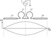
本发明的实施方式涉及的高频磁场产生装置具备至少两个线圈L1、L2。如图1所示,两个线圈L1、L2相隔规定间隔(例如各线圈L1、L2的直径左右)互相平行地配置。另外,试样101配置在作为光检测磁共振材料(以下称为ODMR材料)的具有NVC的金刚石等的板材102上,进而,板材102固定在试样板103上。而且,两个线圈L1、L2夹着作为ODMR材料的具有NVC的板材102而配置。此外,ODMR材料是电子自旋共振材料的一种。The high-frequency magnetic field generator according to the embodiment of the present invention includes at least two coils L1 and L2. As shown in FIG. 1 , the two coils L1 and L2 are arranged in parallel with each other at a predetermined interval (for example, about the diameter of each of the coils L1 and L2 ). In addition, the
两个线圈L1、L2的形状彼此相同,且被配置成具有同一中心轴。另外,此处各线圈L1、L2的匝数大致为一匝(不足一匝)。对两个线圈L1、L2接通微波电流,两个线圈L1、L2分别呈同相(即各时间点的方向相同)地生成作为微波的交变磁场。该交变磁场被施加至ODMR材料,并且施加与线圈L1、L2生成的交变磁场不同的未图示的静磁场。并且,通过未图示的光学系统向ODMR材料照射规定波长的激光等的测量光,并观测例如特定波长的辐射光,从而进行基于光检测磁共振的测量(磁测量、NVC等的方位、NVC等的温度等)。The two coils L1 and L2 have the same shape and are arranged to have the same central axis. Here, the number of turns of each of the coils L1 and L2 is approximately one turn (less than one turn). A microwave current is connected to the two coils L1 and L2, and the two coils L1 and L2 respectively generate alternating magnetic fields as microwaves in the same phase (ie, the same direction at each time point). This alternating magnetic field is applied to the ODMR material, and an unillustrated static magnetic field is applied that is different from the alternating magnetic field generated by the coils L1 and L2. In addition, by irradiating the ODMR material with measurement light such as laser light of a predetermined wavelength by an optical system not shown, and observing, for example, radiation light of a specific wavelength, measurement based on photodetection magnetic resonance (magnetic measurement, orientation such as NVC, NVC, etc.) is carried out. temperature, etc.).
图2是表示本发明第一实施方式涉及的高频磁场产生装置的构成的电路图。2 is a circuit diagram showing the configuration of the high-frequency magnetic field generator according to the first embodiment of the present invention.
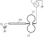
如图2所示,第一实施方式涉及的高频磁场产生装置还具备高频电源1和两个线路体S1、S2。As shown in FIG. 2 , the high-frequency magnetic field generator according to the first embodiment further includes a high-
高频电源1生成导通至两个线圈L1、L2的微波电流。具体来说,高频电源1生成光检测磁共振所需的频带(此处为2.87GHz左右)的微波电流。The high-
两个线路体S1、S2是分别与两个线圈L1、L2连接的传送线路部,并以使两个线圈L1、L2位于驻波的波节之外的位置处的方式设定电流分布。The two line bodies S1 and S2 are transmission line parts respectively connected to the two coils L1 and L2, and the current distribution is set so that the two coils L1 and L2 are located at positions other than the nodes of the standing wave.
此外,各线路体S1、S2可以作为一根导电体的线路而构成,也可以作为使用电阻元件、电容器元件等的分布参数电路而构成。In addition, each of the circuit bodies S1 and S2 may be configured as a single conductor circuit, or may be configured as a distributed parameter circuit using a resistance element, a capacitor element, or the like.
具体来说,在第一实施方式中,如图2所示,两个线路体S1、S2各自的一端开放,两个线路体S1、S2各自的另一端分别与两个线圈L1、L2各自的一端连接。另外,两个线圈L1、L2各自的另一端相互电连接,其连接点与高频电源1连接。因此,微波电流从高频电源1分别流入两个线圈L1、L2各自的另一端。此外,两个线圈L1、L2的形状彼此相同,线路体S1、S2的形状彼此也相同。通过如此构成,从高频电源1来看,线圈L1和线路体S1与线圈L2和线路体S2具有彼此相同的高频特性(即相同的电长度)。Specifically, in the first embodiment, as shown in FIG. 2 , one end of each of the two circuit bodies S1 and S2 is open, and the other end of each of the two circuit bodies S1 and S2 is connected to the two coils L1 and L2 respectively. connected at one end. In addition, the other ends of the two coils L1 and L2 are electrically connected to each other, and the connection point is connected to the high-
例如,在线圈L1和线路体S1的电长度、以及线圈L2和线路体S2的电长度为λ/4(λ:微波的波长)的情况下,成为图2所示那样的电流分布,线圈L1、L2位于驻波的波腹附近而不是驻波的波节处,线圈L1、L2中流动有足够的微波电流,从而诱发微波磁场。For example, when the electrical length of the coil L1 and the circuit body S1 and the electrical length of the coil L2 and the circuit body S2 are λ/4 (λ: wavelength of microwave), the current distribution as shown in FIG. 2 is obtained, and the coil L1 , L2 is located near the antinode of the standing wave instead of the node of the standing wave, and there are enough microwave currents flowing in the coils L1 and L2 to induce the microwave magnetic field.
例如,在高频电源1生成2.87GHz的微波的情况下,波长约为10cm,因而线圈L1和线路体S1的电长度、以及线圈L2和线路体S2的电长度约为2.5cm。另外,为了容易进行调谐,优选将线圈L1、L2的长度设定在线路体S1、S2的长度的1/2以下。For example, when the high-
接下来,对第一实施方式涉及的高频磁场产生装置的动作进行说明。Next, the operation of the high-frequency magnetic field generator according to the first embodiment will be described.
当高频电源1生成微波的交流电时,微波电流流向线圈L1和线路体S1、以及线圈L2和线路体S2。在此,由于线圈L1和线路体S1的终端、以及线圈L2和线路体S2的终端已经达成阻抗匹配,因此在本实施方式中未采取其他阻抗匹配的措施,在线圈L1和线路体S1、以及线圈L2和线路体S2中形成图2所示那样的驻波。When the high-
由此,线圈L1、L2中导通同相且相同大小的交变电流。通过导通至线圈L1、L2的电流而形成微波磁场。由于线圈L1、L2同轴且大致平行地配置,因此,在线圈L1与线圈L2之间的空间中,磁场的方向与线圈L1、L2的中心轴大致平行,而且磁场大致相同。As a result, the coils L1 and L2 conduct alternating currents of the same phase and the same magnitude. A microwave magnetic field is formed by the current conducted to the coils L1, L2. Since the coils L1 and L2 are arranged coaxially and substantially parallel, in the space between the coil L1 and the coil L2, the direction of the magnetic field is substantially parallel to the central axes of the coils L1 and L2, and the magnetic field is substantially the same.
综上所述,根据上述第一实施方式,两个线圈L1、L2以夹着ODMR材料的方式相隔规定间隔互相平行地配置。高频电源1生成导通至这两个线圈L1、L2的微波电流。两个线路体S1、S2分别与该两个线圈L1、L2连接,并以使该两个线圈L1、L2位于驻波的波节之外的位置处的方式设定电流分布。As described above, according to the above-described first embodiment, the two coils L1 and L2 are arranged parallel to each other with a predetermined interval therebetween so as to sandwich the ODMR material. The high-
由此,在线圈L1与线圈L2之间的空间中的广泛范围内生成大致均匀的三维高频磁场。由此,能够提高ODMR的检测灵敏度。Thereby, a substantially uniform three-dimensional high-frequency magnetic field is generated over a wide range in the space between the coil L1 and the coil L2. Thereby, the detection sensitivity of ODMR can be improved.
此外,在该实施方式中,线路体S1、S2各自的一端开放,但是,也可以在该开放端与接地之间连接例如在同一电源(振荡)频率下具有足够高的阻抗的电路。In this embodiment, one end of each of the line bodies S1 and S2 is open, but a circuit having a sufficiently high impedance at the same power supply (oscillation) frequency, for example, may be connected between the open end and the ground.
另外,如图1所示,两个线圈L1、L2以夹着ODMR材料的方式相隔规定间隔互相平行地配置,但是,也可以将ODMR材料配置在两个线圈L1、L2的一侧。该情况下,虽然共振的频带稍微变窄,但具有ODMR材料的设置自由度变高这一优点。In addition, as shown in FIG. 1, the two coils L1 and L2 are arranged parallel to each other with a predetermined interval therebetween so as to sandwich the ODMR material. However, the ODMR material may be arranged on one side of the two coils L1 and L2. In this case, although the frequency band of resonance is slightly narrowed, there is an advantage that the degree of freedom of installation of the ODMR material is increased.
另外,在图1中,板材102和试样板103被配置为垂直于磁场的方向(线圈L1、L2的中心轴方向),但是,也可以将板材102和试样板103配置为相对于磁场的方向(线圈L1、L2的中心轴方向)倾斜,该情况下也对板材102施加同样的磁场。In addition, in FIG. 1, the
第二实施方式.Second embodiment.
图3是表示本发明第二实施方式涉及的高频磁场产生装置的构成的电路图。第二实施方式涉及的高频磁场产生装置与第一实施方式涉及的高频磁场产生装置具有相同的构成,而且在高频电源1与两个线圈L1、L2之间还设有阻抗匹配部11。3 is a circuit diagram showing a configuration of a high-frequency magnetic field generator according to a second embodiment of the present invention. The high-frequency magnetic field generator according to the second embodiment has the same configuration as the high-frequency magnetic field generator according to the first embodiment, and an
在高频电源1与线圈L1、L2之间未实施阻抗匹配的情况下,来自高频电源1的微波会被线圈L1、L2反射,从而在线圈L1、L2中流动的微波电流不足,因此,在高频电源1与线圈L1、L2之间未实施阻抗匹配的情况下,设置阻抗匹配部11。由此,实施阻抗匹配,将来自高频电源1的微波传输至线圈L1、L2。作为阻抗匹配部11,可以使用例如电阻元件(R)、电容元件(C)、电感元件(L)或者这些元件的组合等。When impedance matching is not performed between the high-
此外,在图3中,阻抗匹配部11配置在线圈L1和线圈L2的连接点与高频电源1之间,但也可以将两个阻抗匹配部11分别配置在线圈L1与高频电源1之间、以及线圈L2与高频电源1之间。In addition, in FIG. 3, the
另外,在后述的其他实施方式涉及的高频磁场产生装置中,当然也可以设置相同的阻抗匹配部。届时,在高频电源1与两个线路体连接的情况下,也可以在高频电源1与两个线路体之间设置同样的阻抗匹配部。In addition, it goes without saying that the same impedance matching portion may be provided in the high-frequency magnetic field generators according to other embodiments described later. At this time, when the high-
综上所述,根据上述第二实施方式,即使在仅仅依靠线圈L1、L2或者线路体S1、S2未能达成阻抗匹配的情况下,也能够通过上述阻抗匹配部11来实现阻抗匹配。As described above, according to the second embodiment, even if impedance matching cannot be achieved only by the coils L1 and L2 or the circuit bodies S1 and S2 , the
第三实施方式.third embodiment.
图4是表示本发明第三实施方式涉及的高频磁场产生装置的构成的电路图。第三实施方式涉及的高频磁场产生装置具备至少两对线圈(L1-i、L2-i)(i=1、……、n;n>1)和至少两个线路体S1-j、S2-j,其中,该至少两个线路体S1-j、S2-j包含位于该至少两对线圈各自的一方线圈L1-i彼此间的线路体S1-j、和位于该至少两对线圈各自的另一方线圈L2-i彼此间的线路体S2-j。4 is a circuit diagram showing a configuration of a high-frequency magnetic field generating device according to a third embodiment of the present invention. The high-frequency magnetic field generator according to the third embodiment includes at least two pairs of coils (L1-i, L2-i) (i=1, . . . , n; n>1) and at least two circuit bodies S1-j, S2 -j, wherein the at least two circuit bodies S1-j, S2-j include a circuit body S1-j located between one coil L1-i of each of the at least two pairs of coils, and a circuit body S1-j located between each of the at least two pairs of coils The circuit body S2-j between the other coils L2-i.
在第三实施方式中,高频电源1生成导通至上述至少两对线圈(L1-i、L2-i)(i=1、……、n)中各自成对的两个线圈L1-i、L2-i的微波电流。In the third embodiment, the high-
上述至少两对线圈(L1-i、L2-i)的每一对均以夹着ODMR材料的方式相隔规定间隔互相平行地配置。例如,线圈L1-1~L1-n被配置为诱发的微波磁场同相,线圈L2-1~L2-n被配置为诱发的微波磁场同相。即,通过线圈L1-1~L1-n、L2-1~L2-n诱发的微波磁场的方向相同。Each of the at least two pairs of coils ( L1 - i , L2 - i ) is arranged parallel to each other at a predetermined interval so as to sandwich the ODMR material. For example, the coils L1-1 to L1-n are configured so that the induced microwave magnetic fields are in phase, and the coils L2-1 to L2-n are configured so that the induced microwave magnetic fields are in phase. That is, the directions of the microwave magnetic fields induced by the coils L1-1 to L1-n and L2-1 to L2-n are the same.
另外,上述至少两个线路体S1-j、S2-j是以使至少两对线圈L1-i、L2-i中的各线圈位于驻波的波节之外的位置处的方式设定电流分布的传送线路部。例如,将所有的线路体S1-j、S2-j的电长度全部设置为同一长度,且使线路体S1-j与线圈L1-j交替配置、线路体S2-j与线圈L2-j交替配置。具体来说,线路体S1-j配置在线圈L1-j与线圈L1-(j+1)之间,线路体S2-j配置在线圈L2-j与线圈L2-(j+1)之间,末端的线路体S1-n和线路体S2-n的终端分别开放。In addition, the above-mentioned at least two circuit bodies S1-j and S2-j are set such that the current distribution is set so that each of the at least two pairs of coils L1-i and L2-i is located at a position other than the node of the standing wave of the transmission line. For example, the electrical lengths of all the circuit bodies S1-j and S2-j are all set to the same length, and the circuit bodies S1-j and the coils L1-j are alternately arranged, and the circuit bodies S2-j and the coils L2-j are alternately arranged . Specifically, the circuit body S1-j is arranged between the coil L1-j and the coil L1-(j+1), the circuit body S2-j is arranged between the coil L2-j and the coil L2-(j+1), The terminals of the line body S1-n and the line body S2-n at the end are respectively opened.
例如,线圈L1-i、L2-i具有相同的形状,且被配置成具有相同的中心轴。在此,在各线圈L1-i、L2-i的匝数大致为一匝(不足一匝),且线圈L1-1~L1-n及其之间的线路体S1-j的电长度、和线圈L2-1~L2-n及其之间的线路体S2-j的电长度为(2n-1)λ/4时,成为图4所示那样的电流分布,所有的线圈L1-i、L2-i位于驻波的波节之外的位置处,线圈L1-i、L2-i中流动有足够的微波电流,从而诱发微波磁场。For example, the coils L1-i and L2-i have the same shape and are arranged to have the same central axis. Here, the number of turns in each of the coils L1-i and L2-i is approximately one turn (less than one turn), and the electrical lengths of the coils L1-1 to L1-n and the circuit body S1-j between them, and When the electrical length of the coils L2-1 to L2-n and the circuit body S2-j between them is (2n-1)λ/4, the current distribution as shown in FIG. 4 is obtained, and all the coils L1-i, L2 -i is located at a position outside the node of the standing wave, and sufficient microwave current flows in the coils L1-i, L2-i to induce a microwave magnetic field.
综上所述,根据上述第三实施方式,因为线圈L1-i、L2-i的数量较多,因而可以提高诱发的高频磁场的强度。In summary, according to the third embodiment described above, since the number of coils L1-i and L2-i is large, the intensity of the induced high-frequency magnetic field can be increased.
第四实施方式.Fourth Embodiment.
图5是表示本发明第四实施方式涉及的高频磁场产生装置的构成的电路图。如图5所示,第四实施方式涉及的高频磁场产生装置具备两对线圈(L11、L21)、(L12、L22)、和作为传送线路部的两个线路体S11、S21。5 is a circuit diagram showing a configuration of a high-frequency magnetic field generating device according to a fourth embodiment of the present invention. As shown in FIG. 5 , the high-frequency magnetic field generator according to the fourth embodiment includes two pairs of coils (L11, L21), (L12, L22), and two line bodies S11, S21 as transmission line parts.
图6是对本发明第四实施方式涉及的高频磁场产生装置中的线圈L11、L21、L12、L22的配置的一例进行说明的立体图。如图6所示,各线圈L11、L21、L12、L22的匝数大致为半匝,线圈L11和线圈L22成一对,且呈同相地诱发微波磁场,线圈L12和线圈L21成一对,且呈同相地诱发微波磁场。6 is a perspective view illustrating an example of the arrangement of coils L11 , L21 , L12 , and L22 in the high-frequency magnetic field generator according to the fourth embodiment of the present invention. As shown in FIG. 6 , the number of turns of each coil L11, L21, L12, and L22 is approximately half turns, the coil L11 and the coil L22 form a pair, and induce a microwave magnetic field in the same phase, and the coil L12 and the coil L21 form a pair and are in the same phase. ground induced microwave magnetic field.
此外,也可以使各线圈L11、L21、L12、L22的匝数与第一~第三实施方式同样大致为一匝,并使同相的线圈L11、L22互相靠近而配置(即合计约为两匝),使同相的线圈L12、L21互相靠近而配置。In addition, the number of turns of each of the coils L11, L21, L12, and L22 may be approximately one turn as in the first to third embodiments, and the coils L11 and L22 of the same phase may be arranged close to each other (that is, approximately two turns in total). ), the coils L12 and L21 of the same phase are arranged close to each other.
另外,在第四实施方式中,两个线圈L12、L22各自的一端接地,两个线圈L12、L22各自的另一端分别与两个线路体S11、S21各自的一端连接,另外,两个线路体S11、S21各自的另一端与两个线圈L11、L21各自的一端连接,两个线圈L11、L21各自的另一端相互连接,其连接点与高频电源1连接。于是,微波电流从高频电源1经由线圈L11、L21分别流入两个线路体S11、S21各自的另一端。因此,线圈L12、L22的一端(短路的端部)成为电流分布的波腹,如图5所示,各线圈L11、L12、L21、L22位于电流分布的波节之外的位置上。In the fourth embodiment, one end of each of the two coils L12 and L22 is grounded, and the other end of each of the two coils L12 and L22 is connected to one end of each of the two circuit bodies S11 and S21, respectively. The other ends of each of S11 and S21 are connected to one end of each of the two coils L11 and L21 , the other ends of each of the two coils L11 and L21 are connected to each other, and the connection point is connected to the high
第五实施方式.Fifth Embodiment.
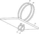
图7是对本发明第五实施方式涉及的高频磁场产生装置中的线圈及线路体进行说明的立体图。7 is a perspective view illustrating a coil and a circuit body in a high-frequency magnetic field generator according to a fifth embodiment of the present invention.
第五实施方式涉及的高频磁场产生装置具备第一实施方式或第二实施方式(图2或图3)所示的电路构成,且具备基板21。而且,两个线圈L1、L2以大致垂直的方式配置在基板21的一面上。另外,在该第五实施方式中,两个线路体S1、S2分别为切口环状的线路部材,且以大致垂直的方式配置在基板21的另一面上。The high-frequency magnetic field generator according to the fifth embodiment includes the circuit configuration shown in the first embodiment or the second embodiment ( FIG. 2 or FIG. 3 ), and includes a
而且,如图2或图3所示,线圈L1、L2、线路体S1、S2以及高频电源1电连接,该电连接通过基板21上的配线图案、基板21上的通孔等进行。Furthermore, as shown in FIG. 2 or FIG. 3 , the coils L1 , L2 , the circuit bodies S1 , S2 , and the high-
此外,第五实施方式涉及的高频磁场产生装置的动作与第一实施方式或第二实施方式相同,故省略其说明。In addition, since the operation of the high-frequency magnetic field generator according to the fifth embodiment is the same as that of the first embodiment or the second embodiment, the description thereof is omitted.
第六实施方式.Sixth Embodiment.
图8是对本发明第六实施方式涉及的高频磁场产生装置中的线圈和线路体进行说明的立体图。8 is a perspective view illustrating a coil and a circuit body in a high-frequency magnetic field generator according to a sixth embodiment of the present invention.
第六实施方式涉及的高频磁场产生装置具有第一实施方式或第二实施方式(图2或图3)所示的电路构成,且具备基板21。而且,两个线圈L1、L2以大致垂直的方式配置在基板21的一面上。另外,在该第六实施方式中,两个线路体S1、S2分别为配线图案,且形成于基板21的任意一个面上。The high-frequency magnetic field generator according to the sixth embodiment has the circuit configuration shown in the first embodiment or the second embodiment ( FIG. 2 or FIG. 3 ), and includes a
图9是表示本发明第六实施方式涉及的高频磁场产生装置中的线路体的另一例的立体图。如图9所示,也可以在线路体S1、S2上分别设置彼此相同的支路31、32。通过如此构成,可以在线圈L1、L2和线路体S1、S2中调整电流分布,而且还可以调整输入带宽。9 is a perspective view showing another example of the circuit body in the high-frequency magnetic field generator according to the sixth embodiment of the present invention. As shown in FIG. 9 , the
此外,第六实施方式涉及的高频磁场产生装置的动作与第一实施方式或第二实施方式相同,故省略其说明。In addition, the operation of the high-frequency magnetic field generating device according to the sixth embodiment is the same as that of the first embodiment or the second embodiment, so the description thereof is omitted.
第七实施方式.Seventh embodiment.
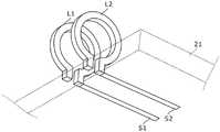
图10是对本发明第七实施方式涉及的高频磁场产生装置中的线圈和线路体进行说明的立体图。10 is a perspective view illustrating a coil and a circuit body in a high-frequency magnetic field generator according to a seventh embodiment of the present invention.
第七实施方式涉及的高频磁场产生装置具备第四实施方式(图5)所示的电路构成,且具备基板21。如图10所示,在第七实施方式中,在基板21上,以相对于基板21垂直的方式设置有线圈L11、L12、L21、L22,并且,线圈L11的一端和线圈L12的一端上连接有切口环状的线路体S11,线圈L21的一端和线圈L22的一端上连接有切口环状的线路体S21。The high-frequency magnetic field generator according to the seventh embodiment includes the circuit configuration shown in the fourth embodiment ( FIG. 5 ), and includes a
如图10所示,线路体S11、S21相对于线圈L11、L22的开口方向以及线圈L12、L21的开口方向(即,由线圈L11、L22、L12、L21形成的磁场的方向)垂直地配置,从而线圈L11、L22、L12、L21与线路体S11、S21不易磁耦合。As shown in FIG. 10, the circuit bodies S11 and S21 are arranged perpendicular to the opening directions of the coils L11 and L22 and the opening directions of the coils L12 and L21 (that is, the directions of the magnetic fields formed by the coils L11, L22, L12 and L21), Therefore, the coils L11, L22, L12, L21 and the circuit bodies S11, S21 are not easily magnetically coupled.
此外,第七实施方式涉及的高频磁场产生装置的动作与第四实施方式相同,故省略其说明。In addition, since the operation of the high-frequency magnetic field generator according to the seventh embodiment is the same as that of the fourth embodiment, the description thereof is omitted.
第八实施方式.Eighth embodiment.
图11是表示本发明第八实施方式涉及的高频磁场产生装置的构成的电路图。11 is a circuit diagram showing a configuration of a high-frequency magnetic field generating device according to an eighth embodiment of the present invention.
在第八实施方式涉及的高频磁场产生装置中,如图11所示,两个线圈L1、L2并联连接,两个线圈L1、L2的连接点上连接有作为传送线路部的一个线路体S1s。在第八实施方式中,通过一个线路体S1s以使两个线圈L1、L2位于驻波的波节之外的位置处的方式设定电流分布。In the high-frequency magnetic field generator according to the eighth embodiment, as shown in FIG. 11 , two coils L1 and L2 are connected in parallel, and one line body S1s as a transmission line portion is connected to the connection point of the two coils L1 and L2 . In the eighth embodiment, the current distribution is set by one line body S1s so that the two coils L1 and L2 are located at positions other than the nodes of the standing wave.
具体来说,在第八实施方式中,如图11所示,线路体S1s的一端开放,线路体S1s的另一端与两个线圈L1、L2的一个连接点连接。另外,两个线圈L1、L2的另一个连接点与高频电源1连接。因此,微波电流从高频电源1流入两个线圈L1、L2各自的另一端。此外,两个线圈L1、L2的形状彼此相同。通过如此构成,从高频电源1来看,线圈L1和线路体S1s与线圈L2和线路体S1s具有彼此相同的高频特性(即相同的电长度)。Specifically, in the eighth embodiment, as shown in FIG. 11 , one end of the line body S1s is open, and the other end of the line body S1s is connected to one connection point of the two coils L1 and L2. In addition, the other connection point of the two coils L1 and L2 is connected to the high-
例如,在线圈L1、L2以及线路体S1s的电长度为λ/4(λ:微波的波长)的情况下,成为图11所示那样的电流分布,线圈L1、L2位于驻波的波腹附近而不是驻波的波节处,线圈L1、L2中流动有足够的微波电流,从而诱发微波磁场。For example, when the electrical lengths of the coils L1 and L2 and the circuit body S1s are λ/4 (λ: wavelength of microwave), the current distribution as shown in FIG. 11 is obtained, and the coils L1 and L2 are located near the antinodes of the standing wave. Instead of the nodes of the standing wave, enough microwave currents flow in the coils L1 and L2 to induce a microwave magnetic field.
此外,第八实施方式涉及的高频磁场产生装置的动作与第一实施方式相同,故省略其说明。In addition, since the operation of the high-frequency magnetic field generator according to the eighth embodiment is the same as that of the first embodiment, the description thereof is omitted.
此外,图11所示的第八实施方式涉及的的高频磁场产生装置的构成,也可以采用图12或图13所示的变形例。In addition, the configuration of the high-frequency magnetic field generating device according to the eighth embodiment shown in FIG. 11 may be the modified example shown in FIG. 12 or FIG. 13 .
图12是表示本发明第八实施方式的变形例1涉及的高频磁场产生装置的构成的电路图。在图12所示的变形例1中,线路体S1s的未与线圈L1、L2连接的一端与可变电容元件41的一端连接,该可变电容元件41的另一端接地。由此,即使从中心轴发生偏离,也可以通过使该可变电容元件41的静电容量发生变动,从而调整为线圈L1、L2的共振频率的中心无限接近于所希望的频率。另外,该可变电容元件41只要具有非常小的静电容量值即可,例如,也可以是使线路体S1s的一部分的位置稍微移动这样的可动装置。或者,该可变电容元件41也可以为例如具有微小的静电容量的可变电容器等。12 is a circuit diagram showing a configuration of a high-frequency magnetic field generator according to
图13是表示本发明第八实施方式的变形例2涉及的高频磁场产生装置的构成的电路图。在图13所示的变形例2中,线圈L1、L2的未与线路体S1s连接的另一端(即电源侧)与可变电容元件51的一端连接,该可变电容元件51的另一端接地。由此,与上述变形例1同样地,即使例如线圈L1、L2的形状发生变化、或者从中心轴发生偏离,也可以通过使该可变电容元件51的静电容量发生变动,从而调整为线圈L1、L2的共振频率的中心无限接近于所希望的频率。另外,该可变电容元件51只要具有非常小的静电容量值即可,例如,也可以为具有微小的静电容量的可变电容器、或者使电源与线圈L1、L2之间的导电线的一部分移动的装置等。13 is a circuit diagram showing a configuration of a high-frequency magnetic field generator according to Modification 2 of the eighth embodiment of the present invention. In Modification 2 shown in FIG. 13 , the other ends (ie, the power supply side) of the coils L1 and L2 that are not connected to the circuit body S1s are connected to one end of the
第九实施方式.Ninth embodiment.
图14是表示本发明第九实施方式涉及的高频磁场产生装置的构成的电路图。14 is a circuit diagram showing a configuration of a high-frequency magnetic field generating device according to a ninth embodiment of the present invention.
在第九实施方式涉及的高频磁场产生装置中,如图14所示,两个线圈L1、L2并联连接,两个线圈L1、L2的连接点上连接有作为传送线路部的一个线路体S1s。在第九实施方式中,通过一个线路体S1s,以使两个线圈L1、L2位于驻波的波节之外的位置处的方式设定电流分布。In the high-frequency magnetic field generating device according to the ninth embodiment, as shown in FIG. 14 , two coils L1 and L2 are connected in parallel, and one line body S1s serving as a transmission line portion is connected to the connection point of the two coils L1 and L2 . In the ninth embodiment, the current distribution is set by one line body S1s so that the two coils L1 and L2 are located at positions other than the nodes of the standing wave.
具体来说,在第九实施方式中,如图14所示,线路体S1s的一端经由一个阻抗匹配部11与高频电源1连接,线路体S1s的另一端连接在两个线圈L1、L2的一个连接点上。另外,两个线圈L1、L2的另一个连接点与另一个阻抗匹配部11的一端部连接。进而,另一个阻抗匹配部11的另一端部开放。因此,微波电流从高频电源1通过一个阻抗匹配部11和线路体S1s流入两个线圈L1、L2各自的一端。此外,两个线圈L1、L2的形状彼此相同。通过如此构成,从高频电源1来看,线圈L1和线路体S1s与线圈L2和线路体S1s具有彼此相同的高频特性(即相同的电长度)。Specifically, in the ninth embodiment, as shown in FIG. 14 , one end of the circuit body S1s is connected to the high-
例如,在线圈L1、L2以及线路体S1s的电长度为λ/4(λ:微波的波长)的情况下,成为图14所示那样的电流分布,线圈L1、L2位于驻波的波腹附近而不是驻波的波节上,线圈L1、L2中流动有足够的微波电流,从而诱发微波磁场。For example, when the electrical lengths of the coils L1 and L2 and the circuit body S1s are λ/4 (λ: wavelength of microwave), the current distribution as shown in FIG. 14 is obtained, and the coils L1 and L2 are located near the antinodes of the standing wave. Instead of the nodes of the standing wave, enough microwave currents flow in the coils L1 and L2 to induce a microwave magnetic field.
第十实施方式.tenth embodiment.
图15是表示本发明第十实施方式涉及的高频磁场产生装置的构成的电路图。15 is a circuit diagram showing a configuration of a high-frequency magnetic field generating device according to a tenth embodiment of the present invention.
在第十实施方式涉及的高频磁场产生装置中,如图15所示,两个线圈L1、L2并联连接,两个线圈L1、L2的连接点上分别连接有作为传送线路部的线路体S1s。在第十实施方式中,通过两个线路体S1s,以使两个线圈L1、L2位于驻波的波节之外的位置处的方式设定电流分布。In the high-frequency magnetic field generator according to the tenth embodiment, as shown in FIG. 15 , two coils L1 and L2 are connected in parallel, and a line body S1s serving as a transmission line portion is connected to the connection points of the two coils L1 and L2, respectively. . In the tenth embodiment, the current distribution is set by the two circuit bodies S1s so that the two coils L1 and L2 are located at positions other than the nodes of the standing wave.
具体来说,在第十实施方式中,如图15所示,一个线路体S1s的一端经由一个阻抗匹配部11与高频电源1连接,一个线路体S1s的另一端连接在两个线圈L1、L2的一个连接点上。另外,两个线圈L1、L2的另一个连接点与另一个线路体S1s的一端连接。另外,另一个线路体的另一端连接在另一个阻抗匹配部11的一端部上。进而,第二阻抗匹配部11的另一端部开放。因此,微波电流从高频电源1通过第一阻抗匹配部11和一个线路体S1s流入两个线圈L1、L2各自的一端。此外,两个线圈L1、L2的形状彼此相同,两个线路体S1s、S1s的形状彼此也相同。通过如此构成,从高频电源1来看,线圈L1和两个线路体S1s与线圈L2和两个线路体S1s具有彼此相同的高频特性(即相同的电长度)。Specifically, in the tenth embodiment, as shown in FIG. 15 , one end of one line body S1s is connected to the high-
例如,在线圈L1、L2以及两个线路体S1s的电长度为λ/2(λ:微波的波长)的情况下,成为如图15所示那样的电流分布,线圈L1、L2位于驻波的波腹附近而不是驻波的波节上,线圈L1、L2中流动有足够的微波电流,从而诱发微波磁场。For example, when the electrical lengths of the coils L1 and L2 and the two circuit bodies S1s are λ/2 (λ: wavelength of microwave), the current distribution as shown in FIG. 15 is obtained, and the coils L1 and L2 are located in the position of the standing wave. In the vicinity of the antinode rather than the node of the standing wave, enough microwave current flows in the coils L1 and L2 to induce a microwave magnetic field.
第十一实施方式.eleventh embodiment.
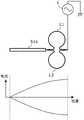
图16是表示本发明第十一实施方式涉及的高频磁场产生装置的构成的图。16 is a diagram showing a configuration of a high-frequency magnetic field generator according to an eleventh embodiment of the present invention.
在该第十一实施方式中,线圈L1、L2以相互平行的金属图案的形式形成于具有规定厚度的基板61的表面和背面上。另外,设有贯穿线圈L1、L2的中心的贯通孔62。通过该贯通孔62,不仅在一对线圈L1、L2两者相隔规定距离配置在试样的一侧的情况下,在试样配置于线圈L1、L2之间的任意位置处的情况下,也能够对试样施加高频交流磁场。In the eleventh embodiment, the coils L1 and L2 are formed in the form of metal patterns parallel to each other on the front and back surfaces of the
进而,如图16所示,也可以在基板61的壁厚内形成与线圈L1、L2的径向平行的贯通孔63、64。该情况下,从贯通孔63射入激光,该光照射在上述贯通孔62内的试样(未图示)上,其反射光经由该贯通孔62朝向上下方向被反射,从而可以通过显微镜进行检测。另一方面,激光中穿过试样的光从贯通孔64射出。因此,也可以观测其射出光。另外,考虑到光的折射问题,也可以使贯通孔64的直径大于贯通孔63的直径。Furthermore, as shown in FIG. 16 , through
另外,在该第十一实施方式中,由于基板61夹在线圈L1与线圈L2之间,因此,稳定地形成线圈L1、L2的形状、稳定地保持两者间的距离等各方面的机械特性和电气性能出色。In addition, in the eleventh embodiment, since the
第十二实施方式.Twelfth Embodiment.
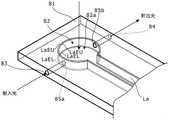
图17是表示本发明第十二实施方式涉及的高频磁场产生装置的构成的图。17 is a diagram showing the configuration of a high-frequency magnetic field generating apparatus according to a twelfth embodiment of the present invention.
在第十二实施方式中,取代第十一实施方式中的上述线圈L1、L2而具备板状线圈La。在具有规定厚度的基板81上设置有贯通孔82。板状线圈La配置于贯通孔内。在第十二实施方式中,板状线圈La以板状线圈La的剖面的长度方向为基板81的垂直方向的方式,固定在基板81的朝向贯通孔82的内壁上。板状线圈La的剖面大致呈矩形。此外,贯通孔82也可以为通孔,板状线圈La可以是通过将例如铜板等薄金属板折弯而形成的线圈,也可以是在作为贯通孔82的通孔的内周面上通过电镀等形成的金属箔。In the twelfth embodiment, a plate-shaped coil La is provided in place of the above-described coils L1 and L2 in the eleventh embodiment. Through
另外,在第十二实施方式中,贯通孔82具有剖面呈圆形的观测孔部82a。并且,板状线圈La的四个边缘部分LaEU、LaEL(尤其是观测孔部82a中的边缘部分)中位于上端侧的边缘部分LaEU的一个和位于下端侧的边缘部分LaEL的一个,作为以夹着电子自旋共振材料的方式相隔规定间隔相互平行地配置、或者相隔规定间隔相互平行地配置在电子自旋共振材料的一侧的两个线圈发挥作用。即,在因为高频(尤其是MHz级以上)引起的趋肤效应的作用下,电流集中流向板状线圈La的边缘部分LaEU、LaEL,因此,实质上上端侧的边缘部分LaEU和下端侧的边缘部分LaEL分别作为线圈发挥作用。此外,优选使板状线圈La的高度(剖面的长边长度)与板状线圈La的圆形部分的半径大致相等,以使与亥姆霍兹线圈的布局相同。另外,为了抑制板状线圈La与显微镜的镜筒之间的寄生电容的变动,优选使板状线圈La的宽度(剖面的短边长度)远小于板状线圈La的高度。In addition, in the twelfth embodiment, the through
另外,通过该贯通孔82,不仅在板状线圈La的上端侧的边缘部分LaEU和下端侧的边缘部分LaEL两者相隔规定距离配置在试样的一侧的情况下,在将试样配置于板状线圈La的上端侧的边缘部分LaEU与下端侧的边缘部分LaEL之间的任意位置处的情况下,也能够对试样施加高频交流磁场。In addition, through the through
进而,如图17所示,也可以在基板81的壁厚内形成有与板状线圈La的圆形部分的径向平行的贯通孔83、84,在贯通孔83、84的延长线上形成板状线圈La的贯通孔85a、85b。该情况下,从贯通孔83和贯通孔85a射入激光,该光照射在上述贯通孔82内的试样(未图示)上,其反射光经由该贯通孔82朝向上下方向被反射,从而可以通过显微镜进行检测。另一方面,激光中穿过试样的光从贯通孔85b和贯通孔84射出。因此,也可以观测该射出光。此外,考虑到光的折射问题,也可以使贯通孔85b、84的直径大于贯通孔83、85a的直径。Furthermore, as shown in FIG. 17 , through
此外,第十二实施方式涉及的高频磁场产生装置的其他构成和动作与第九实施方式和第十一实施方式的任意一个或者两者的组合相同,故省略其说明。In addition, the other configurations and operations of the high-frequency magnetic field generating device according to the twelfth embodiment are the same as those of the ninth embodiment and the eleventh embodiment, or a combination of both, so the description thereof is omitted.
综上所述,根据上述第十二实施方式,通过使用上述板状线圈La,线圈的直流电阻变低。另外,当线圈的周围存在观测用的显微镜的壳体等金属制物体、或者试样台等介电质物体时,因为该等物体的存在而产生的共振频率有可能发生变动,然而,通过使用上述板状线圈La,可以抑制上述共振频率的变动。As described above, according to the above-mentioned twelfth embodiment, by using the above-mentioned plate-shaped coil La, the DC resistance of the coil is reduced. In addition, when there are metal objects such as the casing of a microscope for observation, or dielectric objects such as a sample stage, the resonant frequency may fluctuate due to the presence of these objects. However, by using The above-mentioned plate-shaped coil La can suppress the fluctuation of the above-mentioned resonance frequency.
例如,在基板的厚度为1.6mm、板状线圈La的圆形部分的半径为2mm的情况下,该第十二实施方式中的共振频率在试样配置于贯通孔82内的状态下为2.96GHz,在显微镜的透镜配置于1.5mm的距离处的状态下为2.965GHz。另一方面,在比较例的情况下,在试样配置于贯通孔内的状态下为2.84GHz,在显微镜的透镜配置于1.5mm的距离处的状态下为2.89GHz。由此,共振频率的变动被抑制。For example, when the thickness of the substrate is 1.6 mm and the radius of the circular portion of the plate coil La is 2 mm, the resonance frequency in the twelfth embodiment is 2.96 when the sample is placed in the through
第十三实施方式.Thirteenth Embodiment.
图18是表示本发明第十三实施方式涉及的高频磁场产生装置的构成的图。在第十三实施方式中,贯通孔82呈大致矩形形状,板状线圈La配置在贯通孔82内。在第十三实施方式中,板状线圈La以从基板81的面向贯通孔82的内壁突出的方式被固定。18 is a diagram showing the configuration of a high-frequency magnetic field generating device according to a thirteenth embodiment of the present invention. In the thirteenth embodiment, the through
此外,第十三实施方式涉及的高频磁场产生装置的其他构成和动作与第十二实施方式相同,故省略其说明。In addition, other structures and operations of the high-frequency magnetic field generating device according to the thirteenth embodiment are the same as those of the twelfth embodiment, so the description thereof is omitted.
需要说明的是,关于上述实施方式,也可以在不脱离其主旨和范围且不减弱其所意图的优点的范围内进行各种变更和修改,由于这些变更和修改对于本领域技术人员而言是显而易见的,因而这些变更和修改也应该包含在本申请权利要求的范围内。It should be noted that various changes and modifications can be made to the above-described embodiments without departing from the spirit and scope thereof and without impairing the intended advantages, since these changes and modifications are obvious to those skilled in the art. Obviously, such changes and modifications should also be included within the scope of the claims of the present application.
例如,在上述实施方式中,也可以不使上述两个线路体的端部开放或短路,而以规定的电阻值将两个线路体的端部封闭。For example, in the above-described embodiment, the ends of the two circuit bodies may be closed at a predetermined resistance value without opening or short-circuiting the ends of the two circuit bodies.
另外,在上述第四实施方式中,也可以除去线圈L11、L21,使线路体S11、S21相互连接,并使其连接点与高频电源1连接。In addition, in the above-described fourth embodiment, the coils L11 and L21 may be removed, the circuit bodies S11 and S21 may be connected to each other, and the connection point may be connected to the high-
另外,在上述实施方式中,作为传送线路部而使用线路体,但也可以根据需要将上述线路体替换成集中参数电路。In addition, in the above-described embodiment, the line body is used as the transmission line portion, but the line body may be replaced with a lumped parameter circuit as necessary.
另外,在上述实施方式中,作为ODMR材料而列举了具有NVC的金刚石,但是,也可以取而代之使用其他具有色心(例如SiC色心、或者ZnO、GaN、Si、有机物等色心)的ODMR材料。此外,高频电源1生成与各色心对应的频率的微波电流。In addition, in the above-mentioned embodiment, diamond having NVC is exemplified as the ODMR material, however, other ODMR materials having color centers (for example, SiC color centers, or color centers such as ZnO, GaN, Si, organic substances, etc.) may be used instead. . In addition, the high-
另外,在上述实施方式中,高频磁场产生装置可以在与线圈的开口面积大致相等的区域内形成均匀的磁场。因此,尤其在100MHz以上的高频区域中,虽然适用于ODMR,但也可以适用于EDMR等利用电子自旋共振的其他测量中。图19是表示关于本发明第六实施方式涉及的高频磁场产生装置所发出的磁场的模拟结果的图。在该模拟中,以从电源向线圈L1、L2供给约3GHz的电流的条件实施,其结果是,如图19所示,在从线圈L1、L2的圆心起其开口面积的大致整个区域中产生均匀的磁场(例如从磁场强度的中心值具有10%的误差的区域)。In addition, in the above-described embodiment, the high-frequency magnetic field generating device can form a uniform magnetic field in a region substantially equal to the opening area of the coil. Therefore, although it is suitable for ODMR especially in the high frequency region of 100 MHz or more, it can also be applied to other measurements using electron spin resonance such as EDMR. 19 is a diagram showing a simulation result of the magnetic field generated by the high-frequency magnetic field generator according to the sixth embodiment of the present invention. This simulation was carried out under the condition that a current of about 3 GHz was supplied from the power source to the coils L1 and L2. As a result, as shown in FIG. 19 , the occurrence of a A uniform magnetic field (eg an area with a 10% error from the central value of the magnetic field strength).
另外,在100MHz以下的区域中,也可以与现有的线圈型振荡器同样地使用本发明的各实施方式涉及的高频磁场产生装置。In addition, in the region of 100 MHz or less, the high-frequency magnetic field generating device according to each embodiment of the present invention can be used similarly to the conventional coil-type oscillator.
(工业上的可利用性)(Industrial Availability)
本发明可以适用于例如光检测磁共振用的高频磁场产生装置。The present invention can be applied to, for example, a high-frequency magnetic field generator for photodetection magnetic resonance.
Claims (7)
Applications Claiming Priority (5)
| Application Number | Priority Date | Filing Date | Title |
|---|---|---|---|
| JP2017174895 | 2017-09-12 | ||
| JP2017-174895 | 2017-09-12 | ||
| JP2018-038182 | 2018-03-05 | ||
| JP2018038182AJP7112652B2 (en) | 2017-09-12 | 2018-03-05 | High frequency magnetic field generator |
| CN201810921098.2ACN109490804B (en) | 2017-09-12 | 2018-08-14 | High-frequency magnetic field generating device |
Related Parent Applications (1)
| Application Number | Title | Priority Date | Filing Date |
|---|---|---|---|
| CN201810921098.2ADivisionCN109490804B (en) | 2017-09-12 | 2018-08-14 | High-frequency magnetic field generating device |
Publications (2)
| Publication Number | Publication Date |
|---|---|
| CN114779141Atrue CN114779141A (en) | 2022-07-22 |
| CN114779141B CN114779141B (en) | 2025-05-23 |
Family
ID=63452477
Family Applications (4)
| Application Number | Title | Priority Date | Filing Date |
|---|---|---|---|
| CN202210448222.4AActiveCN114779139B (en) | 2017-09-12 | 2018-08-14 | High frequency magnetic field generating device |
| CN202210448981.0AActiveCN114779141B (en) | 2017-09-12 | 2018-08-14 | High-frequency magnetic field generating device |
| CN201810921098.2AActiveCN109490804B (en) | 2017-09-12 | 2018-08-14 | High-frequency magnetic field generating device |
| CN202210448664.9AActiveCN114779140B (en) | 2017-09-12 | 2018-08-14 | High frequency magnetic field generator |
Family Applications Before (1)
| Application Number | Title | Priority Date | Filing Date |
|---|---|---|---|
| CN202210448222.4AActiveCN114779139B (en) | 2017-09-12 | 2018-08-14 | High frequency magnetic field generating device |
Family Applications After (2)
| Application Number | Title | Priority Date | Filing Date |
|---|---|---|---|
| CN201810921098.2AActiveCN109490804B (en) | 2017-09-12 | 2018-08-14 | High-frequency magnetic field generating device |
| CN202210448664.9AActiveCN114779140B (en) | 2017-09-12 | 2018-08-14 | High frequency magnetic field generator |
Country Status (3)
| Country | Link |
|---|---|
| US (4) | US10921413B2 (en) |
| EP (2) | EP3454053B1 (en) |
| CN (4) | CN114779139B (en) |
Families Citing this family (4)
| Publication number | Priority date | Publication date | Assignee | Title |
|---|---|---|---|---|
| CN114779139B (en)* | 2017-09-12 | 2025-05-27 | 胜美达集团株式会社 | High frequency magnetic field generating device |
| JP7265699B2 (en) | 2019-02-22 | 2023-04-27 | スミダコーポレーション株式会社 | measuring device |
| JP7447844B2 (en)* | 2021-02-23 | 2024-03-12 | 株式会社デンソー | Magnetic field generator and magnetic sensor equipped with it |
| CN114360842B (en)* | 2021-12-28 | 2022-11-22 | 中国人民解放军海军工程大学 | Light periodic magnetic field coil applied to high-power microwave source |
Citations (7)
| Publication number | Priority date | Publication date | Assignee | Title |
|---|---|---|---|---|
| JP2002052006A (en)* | 2000-08-11 | 2002-02-19 | Toshiba Corp | High frequency coil for nuclear magnetic resonance imaging apparatus and nuclear magnetic resonance imaging apparatus |
| CN1696727A (en)* | 2004-05-14 | 2005-11-16 | 西门子公司 | Magnetic field generator and magnetic resonance apparatus having the same |
| JP2006322755A (en)* | 2005-05-17 | 2006-11-30 | Yamagata Promotional Organization For Industrial Technology | Coil device for electron spin resonance |
| CN102958432A (en)* | 2010-08-17 | 2013-03-06 | 株式会社日立医疗器械 | High-frequency coil and magnetic resonance imaging device employing same |
| US20130134979A1 (en)* | 2011-11-28 | 2013-05-30 | The Texas A&M University System | Volume Array Coil with Enforced Uniform Element Currents for Improved Excitation Homogeneity |
| CN103620433A (en)* | 2011-06-22 | 2014-03-05 | 佳能电子株式会社 | Magnetic field detection method and magnetic field detection circuit |
| US20150241529A1 (en)* | 2014-02-21 | 2015-08-27 | Children's Hospital Medical Center | Loop Coil with Integrated Balun for MR Applications |
Family Cites Families (29)
| Publication number | Priority date | Publication date | Assignee | Title |
|---|---|---|---|---|
| JPS60161552A (en)* | 1984-02-01 | 1985-08-23 | Hitachi Ltd | Measuring method of static magnetic field intensity distribution of nmr inspection apparatus |
| JPS63118648A (en)* | 1986-11-07 | 1988-05-23 | Jeol Ltd | Electron spin resonating device provided with loop gap resonator |
| JPS63231251A (en)* | 1987-03-20 | 1988-09-27 | Hitachi Ltd | electron spin resonance device |
| US5024229A (en)* | 1987-11-16 | 1991-06-18 | The University Of Rochester | Resonators for magnetic resonance imaging |
| JPH0666908A (en)* | 1992-08-13 | 1994-03-11 | Mitsubishi Electric Corp | Esr device |
| JP3310519B2 (en)* | 1995-12-28 | 2002-08-05 | 日本電子株式会社 | Resonance frequency adjustment mechanism of loop gap resonator |
| JPH10104181A (en)* | 1996-09-27 | 1998-04-24 | Yamagata Pref Gov Technopolis Zaidan | Electron spin resonance measuring method and electron spin resonance measuring apparatus |
| GB2327762A (en)* | 1997-07-29 | 1999-02-03 | Marconi Gec Ltd | MRI magnet with shuttling HTSC prepolarising block |
| JP2001108732A (en)* | 1999-10-07 | 2001-04-20 | Jeol Ltd | Electron spin resonance apparatus and sample holder for electron spin resonance apparatus |
| US6943550B2 (en)* | 2003-05-09 | 2005-09-13 | The University Of Hong Kong | High temperature superconductor tape RF coil for magnetic resonance imaging |
| WO2007129429A1 (en)* | 2006-05-09 | 2007-11-15 | Hitachi, Ltd. | Magnetic resonance imaging apparatus |
| JP2008002933A (en)* | 2006-06-22 | 2008-01-10 | Jeol Ltd | Loop gap resonator |
| DE102006045174A1 (en)* | 2006-09-25 | 2008-04-03 | Siemens Ag | Method for manufacturing contrast-improved image data set of analysis range of patient, involves loading image data set of analysis range, by which healthy tissue with lower intensity is represented as blood and deficient tissue |
| US7642779B2 (en)* | 2007-03-22 | 2010-01-05 | Kabushiki Kaisha Toshiba | MRI RF coil configured to decouple coil elements and MRI apparatus employing the same |
| DE102008007048B4 (en)* | 2008-01-31 | 2010-06-17 | Siemens Aktiengesellschaft | Dynamic distortion correction in EPI measurements in medical magnetic resonance imaging |
| JP2010249761A (en)* | 2009-04-20 | 2010-11-04 | Kobe Steel Ltd | Probe for nmr |
| CN102612657B (en)* | 2009-09-17 | 2015-11-25 | 皇家飞利浦电子股份有限公司 | For the image intensity correction of magnetic resonance imaging |
| US8674550B2 (en)* | 2010-03-25 | 2014-03-18 | General Electric Company | Contactless power transfer system and method |
| CN103026252B (en)* | 2010-07-23 | 2016-01-06 | 皇家飞利浦电子股份有限公司 | Dual Pressure Sensor Signal Chain for Removing Mutually Coupled MRI Interference |
| JP2012110489A (en) | 2010-11-24 | 2012-06-14 | Sumitomo Electric Ind Ltd | Magnetism measuring instrument, and method for manufacturing magnetism sensor element |
| US9684044B2 (en)* | 2011-11-01 | 2017-06-20 | Hitachi, Ltd. | Magnetic resonance imaging apparatus and antenna device |
| JPWO2013128518A1 (en)* | 2012-02-29 | 2015-07-30 | 日本電気株式会社 | Power transmission device, power reception device, power supply system, and electronic device |
| WO2013145143A1 (en)* | 2012-03-28 | 2013-10-03 | 富士通株式会社 | Power transmitting apparatus |
| CN103105599B (en)* | 2012-05-29 | 2014-12-31 | 辽宁开普医疗系统有限公司 | Magnetic resonance receiving coil with high-speed serial interface |
| US9689954B2 (en)* | 2012-09-28 | 2017-06-27 | William Marsh Rice University | Intergrated electron spin resonance spectrometer |
| JP2014197937A (en)* | 2013-03-29 | 2014-10-16 | 沖電気工業株式会社 | Non-contact power transmission device, non-contact power transmission system, and automatic transaction device |
| US10677953B2 (en)* | 2016-05-31 | 2020-06-09 | Lockheed Martin Corporation | Magneto-optical detecting apparatus and methods |
| CN114779139B (en)* | 2017-09-12 | 2025-05-27 | 胜美达集团株式会社 | High frequency magnetic field generating device |
| CN208422213U (en)* | 2018-01-10 | 2019-01-22 | 上海复旦天欣科教仪器有限公司 | Microwave electron spin resonance experimental provision |
- 2018
- 2018-08-14CNCN202210448222.4Apatent/CN114779139B/enactiveActive
- 2018-08-14CNCN202210448981.0Apatent/CN114779141B/enactiveActive
- 2018-08-14CNCN201810921098.2Apatent/CN109490804B/enactiveActive
- 2018-08-14CNCN202210448664.9Apatent/CN114779140B/enactiveActive
- 2018-08-14USUS16/103,356patent/US10921413B2/enactiveActive
- 2018-08-31EPEP18191872.3Apatent/EP3454053B1/enactiveActive
- 2018-08-31EPEP24185109.6Apatent/EP4414733A3/enactivePending
- 2021
- 2021-01-07USUS17/143,630patent/US11668778B2/enactiveActive
- 2023
- 2023-04-24USUS18/306,109patent/US12248049B2/enactiveActive
- 2025
- 2025-02-04USUS19/044,750patent/US20250189610A1/enactivePending
Patent Citations (7)
| Publication number | Priority date | Publication date | Assignee | Title |
|---|---|---|---|---|
| JP2002052006A (en)* | 2000-08-11 | 2002-02-19 | Toshiba Corp | High frequency coil for nuclear magnetic resonance imaging apparatus and nuclear magnetic resonance imaging apparatus |
| CN1696727A (en)* | 2004-05-14 | 2005-11-16 | 西门子公司 | Magnetic field generator and magnetic resonance apparatus having the same |
| JP2006322755A (en)* | 2005-05-17 | 2006-11-30 | Yamagata Promotional Organization For Industrial Technology | Coil device for electron spin resonance |
| CN102958432A (en)* | 2010-08-17 | 2013-03-06 | 株式会社日立医疗器械 | High-frequency coil and magnetic resonance imaging device employing same |
| CN103620433A (en)* | 2011-06-22 | 2014-03-05 | 佳能电子株式会社 | Magnetic field detection method and magnetic field detection circuit |
| US20130134979A1 (en)* | 2011-11-28 | 2013-05-30 | The Texas A&M University System | Volume Array Coil with Enforced Uniform Element Currents for Improved Excitation Homogeneity |
| US20150241529A1 (en)* | 2014-02-21 | 2015-08-27 | Children's Hospital Medical Center | Loop Coil with Integrated Balun for MR Applications |
Also Published As
| Publication number | Publication date |
|---|---|
| CN114779139B (en) | 2025-05-27 |
| CN109490804B (en) | 2022-05-31 |
| US20210199744A1 (en) | 2021-07-01 |
| CN109490804A (en) | 2019-03-19 |
| US12248049B2 (en) | 2025-03-11 |
| EP3454053B1 (en) | 2024-10-02 |
| CN114779141B (en) | 2025-05-23 |
| EP4414733A3 (en) | 2025-02-05 |
| EP4414733A2 (en) | 2024-08-14 |
| CN114779140A (en) | 2022-07-22 |
| US11668778B2 (en) | 2023-06-06 |
| CN114779140B (en) | 2025-03-18 |
| US20250189610A1 (en) | 2025-06-12 |
| US20230258755A1 (en) | 2023-08-17 |
| EP3454053A1 (en) | 2019-03-13 |
| US10921413B2 (en) | 2021-02-16 |
| CN114779139A (en) | 2022-07-22 |
| US20190079157A1 (en) | 2019-03-14 |
Similar Documents
| Publication | Publication Date | Title |
|---|---|---|
| CN109490804B (en) | High-frequency magnetic field generating device | |
| JP7112652B2 (en) | High frequency magnetic field generator | |
| JP6367236B2 (en) | Resonator for electron spin resonance | |
| US6933725B2 (en) | NMR probe circuit for generating close frequency resonances | |
| US10502797B2 (en) | Crossed-loop resonators | |
| JPH0350541B2 (en) | ||
| WO2022210696A1 (en) | Diamond magneto-optical sensor | |
| JP2018011022A (en) | Oscillation device, calculation device, and measurement method | |
| JP6456865B2 (en) | Structure of NMR transmit / receive coil | |
| Kubo et al. | Ultra-broadband NMR probe: numerical and experimental study of transmission line NMR probe | |
| US20190057318A1 (en) | Compact rf driver for paul traps used in quantum computers and methods of making and using same | |
| Hatzon et al. | Microwave-cavity-mode optimization by background antiresonance tuning | |
| JPS59208910A (en) | Mixer | |
| PL239882B1 (en) | Sample holder for the measurement of optically detected MRI | |
| WO2024180541A1 (en) | A sensor unit and resonator circuit thereof | |
| Chekhovich | Keyhole resonators for subwavelength focusing of microwave magnetic fields in optically detected electron spin resonance | |
| Eisenach | Tunable and broadband loop gap resonator for nitrogen vacancy centers in diamond | |
| Van Ta et al. | An Ultra-high Quality Factor Terahertz Photonic Crystal Cavity | |
| Karkari et al. | Design and performance of a floating hairpin resonance probe for measuring plasma density in radio-frequency discharges | |
| KR20250117685A (en) | Minimal superconducting quantum circuit for bosonic codes with galvanic coupling |
Legal Events
| Date | Code | Title | Description |
|---|---|---|---|
| PB01 | Publication | ||
| PB01 | Publication | ||
| SE01 | Entry into force of request for substantive examination | ||
| SE01 | Entry into force of request for substantive examination | ||
| GR01 | Patent grant | ||
| GR01 | Patent grant |