CN114764155A - Metastics optical device and electronic apparatus including the same - Google Patents
Metastics optical device and electronic apparatus including the sameDownload PDFInfo
- Publication number
- CN114764155A CN114764155ACN202110964676.2ACN202110964676ACN114764155ACN 114764155 ACN114764155 ACN 114764155ACN 202110964676 ACN202110964676 ACN 202110964676ACN 114764155 ACN114764155 ACN 114764155A
- Authority
- CN
- China
- Prior art keywords
- nanostructures
- layer
- index
- refraction
- meta
- Prior art date
- Legal status (The legal status is an assumption and is not a legal conclusion. Google has not performed a legal analysis and makes no representation as to the accuracy of the status listed.)
- Pending
Links
Images


Classifications
- G—PHYSICS
- G02—OPTICS
- G02B—OPTICAL ELEMENTS, SYSTEMS OR APPARATUS
- G02B5/00—Optical elements other than lenses
- G02B5/18—Diffraction gratings
- G02B5/1876—Diffractive Fresnel lenses; Zone plates; Kinoforms
- G—PHYSICS
- G02—OPTICS
- G02B—OPTICAL ELEMENTS, SYSTEMS OR APPARATUS
- G02B1/00—Optical elements characterised by the material of which they are made; Optical coatings for optical elements
- G02B1/002—Optical elements characterised by the material of which they are made; Optical coatings for optical elements made of materials engineered to provide properties not available in nature, e.g. metamaterials
- G—PHYSICS
- G02—OPTICS
- G02B—OPTICAL ELEMENTS, SYSTEMS OR APPARATUS
- G02B3/00—Simple or compound lenses
- G02B3/0087—Simple or compound lenses with index gradient
- G—PHYSICS
- G02—OPTICS
- G02F—OPTICAL DEVICES OR ARRANGEMENTS FOR THE CONTROL OF LIGHT BY MODIFICATION OF THE OPTICAL PROPERTIES OF THE MEDIA OF THE ELEMENTS INVOLVED THEREIN; NON-LINEAR OPTICS; FREQUENCY-CHANGING OF LIGHT; OPTICAL LOGIC ELEMENTS; OPTICAL ANALOGUE/DIGITAL CONVERTERS
- G02F1/00—Devices or arrangements for the control of the intensity, colour, phase, polarisation or direction of light arriving from an independent light source, e.g. switching, gating or modulating; Non-linear optics
- G02F1/01—Devices or arrangements for the control of the intensity, colour, phase, polarisation or direction of light arriving from an independent light source, e.g. switching, gating or modulating; Non-linear optics for the control of the intensity, phase, polarisation or colour
- G02F1/0121—Operation of devices; Circuit arrangements, not otherwise provided for in this subclass
- B—PERFORMING OPERATIONS; TRANSPORTING
- B82—NANOTECHNOLOGY
- B82Y—SPECIFIC USES OR APPLICATIONS OF NANOSTRUCTURES; MEASUREMENT OR ANALYSIS OF NANOSTRUCTURES; MANUFACTURE OR TREATMENT OF NANOSTRUCTURES
- B82Y20/00—Nanooptics, e.g. quantum optics or photonic crystals
- G—PHYSICS
- G02—OPTICS
- G02B—OPTICAL ELEMENTS, SYSTEMS OR APPARATUS
- G02B13/00—Optical objectives specially designed for the purposes specified below
- G02B13/001—Miniaturised objectives for electronic devices, e.g. portable telephones, webcams, PDAs, small digital cameras
- G02B13/0055—Miniaturised objectives for electronic devices, e.g. portable telephones, webcams, PDAs, small digital cameras employing a special optical element
- G—PHYSICS
- G02—OPTICS
- G02B—OPTICAL ELEMENTS, SYSTEMS OR APPARATUS
- G02B26/00—Optical devices or arrangements for the control of light using movable or deformable optical elements
- G02B26/06—Optical devices or arrangements for the control of light using movable or deformable optical elements for controlling the phase of light
- G—PHYSICS
- G02—OPTICS
- G02B—OPTICAL ELEMENTS, SYSTEMS OR APPARATUS
- G02B27/00—Optical systems or apparatus not provided for by any of the groups G02B1/00 - G02B26/00, G02B30/00
- G02B27/0025—Optical systems or apparatus not provided for by any of the groups G02B1/00 - G02B26/00, G02B30/00 for optical correction, e.g. distorsion, aberration
- G02B27/0037—Optical systems or apparatus not provided for by any of the groups G02B1/00 - G02B26/00, G02B30/00 for optical correction, e.g. distorsion, aberration with diffracting elements
- G—PHYSICS
- G02—OPTICS
- G02B—OPTICAL ELEMENTS, SYSTEMS OR APPARATUS
- G02B27/00—Optical systems or apparatus not provided for by any of the groups G02B1/00 - G02B26/00, G02B30/00
- G02B27/42—Diffraction optics, i.e. systems including a diffractive element being designed for providing a diffractive effect
- G02B27/4205—Diffraction optics, i.e. systems including a diffractive element being designed for providing a diffractive effect having a diffractive optical element [DOE] contributing to image formation, e.g. whereby modulation transfer function MTF or optical aberrations are relevant
- G—PHYSICS
- G02—OPTICS
- G02B—OPTICAL ELEMENTS, SYSTEMS OR APPARATUS
- G02B27/00—Optical systems or apparatus not provided for by any of the groups G02B1/00 - G02B26/00, G02B30/00
- G02B27/42—Diffraction optics, i.e. systems including a diffractive element being designed for providing a diffractive effect
- G02B27/4272—Diffraction optics, i.e. systems including a diffractive element being designed for providing a diffractive effect having plural diffractive elements positioned sequentially along the optical path
- G—PHYSICS
- G02—OPTICS
- G02B—OPTICAL ELEMENTS, SYSTEMS OR APPARATUS
- G02B3/00—Simple or compound lenses
- G—PHYSICS
- G02—OPTICS
- G02B—OPTICAL ELEMENTS, SYSTEMS OR APPARATUS
- G02B5/00—Optical elements other than lenses
- G—PHYSICS
- G02—OPTICS
- G02B—OPTICAL ELEMENTS, SYSTEMS OR APPARATUS
- G02B5/00—Optical elements other than lenses
- G02B5/18—Diffraction gratings
- G02B5/1814—Diffraction gratings structurally combined with one or more further optical elements, e.g. lenses, mirrors, prisms or other diffraction gratings
- G02B5/1819—Plural gratings positioned on the same surface, e.g. array of gratings
- G02B5/1823—Plural gratings positioned on the same surface, e.g. array of gratings in an overlapping or superposed manner
- G—PHYSICS
- G02—OPTICS
- G02B—OPTICAL ELEMENTS, SYSTEMS OR APPARATUS
- G02B5/00—Optical elements other than lenses
- G02B5/18—Diffraction gratings
- G02B5/1866—Transmission gratings characterised by their structure, e.g. step profile, contours of substrate or grooves, pitch variations, materials
- G02B5/1871—Transmissive phase gratings
- G—PHYSICS
- G02—OPTICS
- G02F—OPTICAL DEVICES OR ARRANGEMENTS FOR THE CONTROL OF LIGHT BY MODIFICATION OF THE OPTICAL PROPERTIES OF THE MEDIA OF THE ELEMENTS INVOLVED THEREIN; NON-LINEAR OPTICS; FREQUENCY-CHANGING OF LIGHT; OPTICAL LOGIC ELEMENTS; OPTICAL ANALOGUE/DIGITAL CONVERTERS
- G02F1/00—Devices or arrangements for the control of the intensity, colour, phase, polarisation or direction of light arriving from an independent light source, e.g. switching, gating or modulating; Non-linear optics
- G02F1/0009—Materials therefor
- G02F1/0018—Electro-optical materials
- G—PHYSICS
- G02—OPTICS
- G02B—OPTICAL ELEMENTS, SYSTEMS OR APPARATUS
- G02B2207/00—Coding scheme for general features or characteristics of optical elements and systems of subclass G02B, but not including elements and systems which would be classified in G02B6/00 and subgroups
- G02B2207/101—Nanooptics
Landscapes
- Physics & Mathematics (AREA)
- Optics & Photonics (AREA)
- General Physics & Mathematics (AREA)
- Nonlinear Science (AREA)
- Chemical & Material Sciences (AREA)
- Engineering & Computer Science (AREA)
- Nanotechnology (AREA)
- Life Sciences & Earth Sciences (AREA)
- Biophysics (AREA)
- Crystallography & Structural Chemistry (AREA)
- Optical Modulation, Optical Deflection, Nonlinear Optics, Optical Demodulation, Optical Logic Elements (AREA)
- Polarising Elements (AREA)
Abstract
Translated fromChinese
Description
Translated fromChinese相关申请的交叉引用CROSS-REFERENCE TO RELATED APPLICATIONS
本申请基于并要求于2021年1月12日在韩国知识产权局递交的韩国专利申请No.10-2021-0004239的优先权,其全部公开内容通过引用合并于此。This application is based on and claims priority to Korean Patent Application No. 10-2021-0004239 filed in the Korean Intellectual Property Office on Jan. 12, 2021, the entire disclosure of which is incorporated herein by reference.
技术领域technical field
本文阐述的实施例涉及一种超颖光学器件和包括超颖光学器件的电子设备。Embodiments set forth herein relate to a metaoptic device and an electronic device including the metaoptic device.
背景技术Background technique
使用超颖结构的平面衍射元件可以表现出通过使用现有的折射元件不能实现的各种光学效果,并且因此,可以实现薄光学系统。因此,超颖结构已经引起了广泛关注,以用于许多领域。The planar diffractive element using the metastructure can exhibit various optical effects that cannot be realized by using the existing refractive element, and thus, a thin optical system can be realized. Therefore, metastructures have attracted extensive attention for use in many fields.
超颖结构包括具有小于入射光的波长的形状、周期等的纳米结构。为了获得期望的光学性能,纳米结构被设计为满足在每个位置处相对于所期望波段的光设置的相位延迟曲线。当设计纳米结构时,难以在所期望的波段处获得恒定的衍射效率。例如,所期望的波段越宽,中央区域和周边区域之间的衍射效率的差异越大。Metastructures include nanostructures having shapes, periods, etc. smaller than the wavelength of incident light. To obtain the desired optical performance, the nanostructures are designed to satisfy the phase retardation curve set at each location relative to the desired wavelength band of light. When designing nanostructures, it is difficult to obtain constant diffraction efficiency at the desired wavelength band. For example, the wider the desired wavelength band, the greater the difference in diffraction efficiency between the central region and the peripheral region.
发明内容SUMMARY OF THE INVENTION
提供了一种能够在宽带波长下操作并表现出高效率的超颖光学器件。A meta-optical device capable of operating at broadband wavelengths and exhibiting high efficiency is provided.
提供了一种使用超颖光学器件的电子设备。An electronic device using meta-optics is provided.
附加方面部分地将在以下描述中阐述,且部分地将通过该描述而变得清楚明白,或者可以通过实践所呈现的实施例来获知。Additional aspects will be set forth in the following description, and in part will be apparent from the description, or may be learned by practice of the presented embodiments.
根据示例实施例的一方面,一种相对于预定波段的入射光表现出目标相位延迟曲线的超颖光学器件可以包括:第一层,包括多个第一纳米结构和围绕该多个第一纳米结构的第一周围材料,该第一层具有第一趋势的第一相位延迟曲线,该第一趋势与目标相位延迟曲线的趋势基本等同;第二层,被设置为与第一层相邻,并且包括多个第二纳米结构和围绕该多个第二纳米结构的第二周围材料,该第二层具有第二趋势的第二相位延迟曲线,该第二趋势与目标相位延迟曲线的趋势基本相反;以及第三层,被设置为与第二层相邻,并且包括多个第三纳米结构和围绕该多个第三纳米结构的第三周围材料,该第三层具有与第二相位延迟曲线不同的第三相位延迟曲线,其中,该第三层包括与第二层的第二材料不同的第三材料,或者包括与第二层的第二布置规则不同的第三布置规则。According to an aspect of example embodiments, a metaoptic device exhibiting a target phase retardation curve with respect to incident light of a predetermined wavelength band may include: a first layer including a plurality of first nanostructures and surrounding the plurality of first nanostructures a first surrounding material of the structure, the first layer having a first phase retardation curve of a first trend that is substantially identical to the trend of the target phase retardation curve; a second layer, disposed adjacent to the first layer, and comprising a plurality of second nanostructures and a second surrounding material surrounding the plurality of second nanostructures, the second layer has a second phase delay curve of a second trend, the second trend is substantially the same as the trend of the target phase delay curve Conversely; and a third layer disposed adjacent to the second layer and comprising a plurality of third nanostructures and a third surrounding material surrounding the plurality of third nanostructures, the third layer having a phase retardation from the second A third phase retardation curve with a different curve, wherein the third layer includes a third material different from the second material of the second layer, or includes a third arrangement rule different from the second arrangement rule of the second layer.
预定波段可以包括可见光波段或近红外波段。The predetermined wavelength band may include a visible light band or a near-infrared band.
预定波段可以具有基本上大于或等于300纳米的带宽。The predetermined wavelength band may have a bandwidth substantially greater than or equal to 300 nanometers.
预定波段中的最小衍射效率可以基本上大于或等于90%。The minimum diffraction efficiency in the predetermined wavelength band may be substantially greater than or equal to 90%.
预定波段的带宽Δλ与中心波长λ0的比率Δλ/λ0基本上大于或等于15%。The ratio Δλ/λ0 of the bandwidth Δλ of the predetermined band to the center wavelength λ0 is substantially greater than or equal to 15%.
多个第一纳米结构、多个第二纳米结构和多个第三纳米结可以均具有小于预定波段的中心波长的形状尺寸。The plurality of first nanostructures, the plurality of second nanostructures, and the plurality of third nanojunctions may each have a shape dimension smaller than a center wavelength of the predetermined wavelength band.
多个第一纳米结构相对于预定波段的中心波长λ0的高度可以基本上在2λ0至5λ0的范围内。The height of the plurality of first nanostructures relative to the center wavelength λ0 of the predetermined wavelength band may be substantially in the range of 2λ0 to 5λ0 .
多个第一纳米结构的高度与多个第一纳米结构的宽度的比率可以基本上大于2。The ratio of the height of the plurality of first nanostructures to the width of the plurality of first nanostructures may be substantially greater than two.
多个第二纳米结构和多个第三纳米结构相对于预定波段的中心波长λ0的相应高度可以基本上在0.5λ0至2λ0的范围内。The respective heights of the plurality of second nanostructures and the plurality of third nanostructures with respect to the center wavelength λ0 of the predetermined wavelength band may be substantially in the range of 0.5λ0 to 2λ0 .
第一层可以包括多个相位调制区域,在该多个相位调制区域中重复执行特定范围的相位调制,并且其中,第一层的与多个相位调制区域之间的边界相邻的部分未设置有多个第一纳米结构。The first layer may include a plurality of phase modulation regions in which phase modulation of a specific range is repeatedly performed, and wherein a portion of the first layer adjacent to a boundary between the plurality of phase modulation regions is not provided There are a plurality of first nanostructures.
该部分的宽度与对应的相位调制区域的宽度的比率可以基本上大于或等于5%。The ratio of the width of the portion to the width of the corresponding phase modulation region may be substantially greater than or equal to 5%.
第三层的第三材料可以具有比第二层的第二材料低的折射率和低的色散。The third material of the third layer may have a lower refractive index and lower dispersion than the second material of the second layer.
多个第一纳米结构可以具有比第一周围材料的折射率低的折射率,多个第二纳米结构具有比第二周围材料的折射率高的折射率,并且多个第一纳米结构和多个第二纳米结构在远离超颖光学器件的中心的方向上均具有基本相似的宽度变化趋势。The plurality of first nanostructures may have a refractive index lower than that of the first surrounding material, the plurality of second nanostructures may have a higher refractive index than the refractive index of the second surrounding material, and the plurality of first nanostructures and the plurality of Each of the second nanostructures has a substantially similar trend of width variation in the direction away from the center of the meta-optical device.
多个第三纳米结构具有比第三周围材料的折射率大并且比多个第二纳米结构的折射率小的折射率。The plurality of third nanostructures have an index of refraction greater than the index of refraction of the third surrounding material and less than the index of refraction of the second plurality of nanostructures.
超颖光学器件可以包括折射率小于或等于第三周围材料的折射率的基板,并且第三层、第二层和第一层可以被依次布置在基板上。The meta-optic device may include a substrate having an index of refraction less than or equal to that of the third surrounding material, and the third layer, the second layer, and the first layer may be sequentially arranged on the substrate.
超颖光学器件可以包括折射率小于或等于第三周围材料的折射率的基板,并且第三层、第一层和第二层被依次布置在基板上。The meta-optic device may include a substrate having a refractive index less than or equal to that of a third surrounding material, and the third layer, the first layer, and the second layer are sequentially arranged on the substrate.
多个第一纳米结构可以具有比第一周围材料的折射率小的折射率,多个第二纳米结构可以具有比第二周围材料的折射率小的折射率,并且多个第一纳米结构和多个第二纳米结构可以在远离超颖光学器件的中心的方向上具有基本相反的宽度变化趋势。The plurality of first nanostructures may have a refractive index that is less than the refractive index of the first surrounding material, the plurality of second nanostructures may have a refractive index that is less than the refractive index of the second surrounding material, and the plurality of first nanostructures and The plurality of second nanostructures may have substantially opposite width trends in directions away from the center of the meta-optic.
多个第三纳米结构可以具有比第三周围材料的折射率大并且比第二周围材料的折射率小的折射率。The plurality of third nanostructures may have an index of refraction greater than that of the third surrounding material and less than that of the second surrounding material.
超颖光学器件可以包括折射率小于或等于第三周围材料的折射率的基板,并且第三层、第二层和第一层可以被依次布置在基板上。The meta-optic device may include a substrate having an index of refraction less than or equal to that of the third surrounding material, and the third layer, the second layer, and the first layer may be sequentially arranged on the substrate.
第一纳米结构可以具有比第一周围材料的折射率大的折射率,第二纳米结构可以具有比第二周围材料的折射率大的折射率,并且多个第一纳米结构和多个第二纳米结构可以在远离超颖光学器件的中心的方向上具有基本相反的宽度变化趋势。The first nanostructure may have an index of refraction greater than the index of refraction of the first surrounding material, the second nanostructure may have an index of refraction greater than the index of refraction of the second surrounding material, and the plurality of first nanostructures and the plurality of second The nanostructures can have substantially opposite trends in width in the direction away from the center of the metaoptic device.
多个第三纳米结构可以具有比第三周围材料的折射率大并且比多个第二纳米结构的折射率小的折射率。The plurality of third nanostructures may have an index of refraction that is greater than the index of refraction of the third surrounding material and less than the index of refraction of the plurality of second nanostructures.
多个第三纳米结构可以具有比第三周围材料的折射率和第二纳米结构的折射率小的折射率。The plurality of third nanostructures may have an index of refraction less than the index of refraction of the third surrounding material and the index of refraction of the second nanostructures.
多个第一纳米结构、多个第二纳米结构和多个第三纳米结构可以各自具有圆柱形状、多棱柱形状、截锥形状或截多边形形状。The plurality of first nanostructures, the plurality of second nanostructures, and the plurality of third nanostructures may each have a cylindrical shape, a polygonal prism shape, a truncated cone shape, or a truncated polygonal shape.
与多个第一纳米结构、多个第二纳米结构和多个第三纳米结构的相应高度垂直的多个第一纳米结构、多个第二纳米结构和多个第三纳米结构各自的截面可以具有圆形形状、多边形形状、圆环形形状或多边环形形状。The respective cross-sections of the plurality of first nanostructures, the plurality of second nanostructures, and the plurality of third nanostructures that are perpendicular to respective heights of the plurality of first nanostructures, the plurality of second nanostructures, and the plurality of third nanostructures may be Have a circular shape, a polygonal shape, a torus shape, or a polygonal ring shape.
在第一层、第二层和第三层中的每一个处的折射率差可以基本上大于或等于0.2。The refractive index difference at each of the first, second, and third layers may be substantially greater than or equal to 0.2.
根据示例实施例的一方面,一种电子设备可以包括相对于预定波段的入射光表现出目标相位延迟曲线的超颖光学器件,该超颖光学器件包括:第一层,包括多个第一纳米结构和围绕该多个第一纳米结构的第一周围材料,该第一层具有第一趋势的第一相位延迟曲线,该第一趋势与目标相位延迟曲线的趋势基本等同;第二层,被设置为与第一层相邻,并且包括多个第二纳米结构和围绕该多个第二纳米结构的第二周围材料,该第二层具有第二趋势的第二相位延迟曲线,该第二趋势与目标相位延迟曲线的趋势基本相反;以及第三层,被设置为与第二层相邻,并且包括多个第三纳米结构和围绕该多个第三纳米结构的第三周围材料,该第三层具有与第二相位延迟曲线不同的第三相位延迟曲线,其中,该第三层包括与第二层的第二材料不同的第三材料,或者包括与第二层的第二布置规则不同的第三布置规则。According to an aspect of example embodiments, an electronic device may include a meta-optic that exhibits a target phase retardation curve with respect to a predetermined wavelength band of incident light, the meta-optic including: a first layer including a plurality of first nanometers a structure and a first surrounding material surrounding the plurality of first nanostructures, the first layer having a first phase retardation curve of a first trend, the first trend being substantially equal to the trend of the target phase retardation curve; the second layer, being disposed adjacent to the first layer and comprising a second plurality of nanostructures and a second surrounding material surrounding the plurality of second nanostructures, the second layer having a second phase retardation curve of a second trend, the second the trend is substantially opposite to the trend of the target phase retardation curve; and a third layer disposed adjacent to the second layer and comprising a plurality of third nanostructures and a third surrounding material surrounding the plurality of third nanostructures, the The third layer has a third phase retardation curve different from the second phase retardation curve, wherein the third layer includes a third material different from the second material of the second layer, or includes a second arrangement rule from the second layer Different third placement rules.
附图说明Description of drawings
根据结合附图的以下描述,本公开的某些实施例的上述和其他方面、特征以及优点将更加显而易见,在附图中:The above and other aspects, features and advantages of certain embodiments of the present disclosure will be more apparent from the following description taken in conjunction with the accompanying drawings, in which:
图1是示意性地示出了根据示例实施例的超颖光学器件的配置和功能的概念图;FIG. 1 is a conceptual diagram schematically illustrating the configuration and function of a meta-optics according to example embodiments;
图2是图1的超颖光学器件的平面图;Fig. 2 is a plan view of the meta-optical device of Fig. 1;
图3是示出了图1的超颖光学器件的相位延迟层的根据波长和位置的有效折射率和色散的曲线图;3 is a graph showing the effective refractive index and dispersion according to wavelength and position of the phase retardation layer of the metaoptic device of FIG. 1;
图4是示出了图1的超颖光学器件的色散控制层的根据波长和位置的有效折射率和色散的曲线图;FIG. 4 is a graph showing the effective refractive index and dispersion according to wavelength and position of the dispersion control layer of the metaoptic device of FIG. 1;
图5A至图5C是分别示出了图1的超颖光学器件的相位延迟层的相位延迟曲线、图1的超颖光学器件的色散控制层的相位延迟曲线和图1的超颖光学器件的相位延迟曲线的曲线图;5A to 5C are diagrams showing the phase retardation curve of the phase retardation layer of the metaoptic device of FIG. 1 , the phase retardation curve of the dispersion control layer of the metaoptic device of FIG. 1 , and the phase retardation curve of the metaoptic device of FIG. 1 , respectively. A graph of the phase delay curve;
图6是示出了在图1的超颖光学器件中可以采用的单位组件的形状和折射率布置的截面图;6 is a cross-sectional view illustrating the shape and refractive index arrangement of unit components that may be employed in the metaoptic device of FIG. 1;
图7是示出了根据图6的单位组件的大小变化的、关于相位的计算机模拟结果的曲线图;FIG. 7 is a graph showing computer simulation results with respect to phase as a function of size variation of the unit component of FIG. 6;
图8是示出了基于图7的计算机模拟结果的、关于超颖光学器件的透射率和效率的计算机模拟结果的曲线图;FIG. 8 is a graph showing computer simulation results regarding transmittance and efficiency of meta-optics based on the computer simulation results of FIG. 7;
图9是示出了关于比较例的超颖光学器件的透射率和效率的计算机模拟结果的曲线图;9 is a graph showing computer simulation results regarding transmittance and efficiency of meta-optics of comparative examples;
图10是示出了根据示例实施例的超颖光学器件的结构的示意性截面图;10 is a schematic cross-sectional view illustrating a structure of a meta-optic according to example embodiments;
图11A是示出了根据另一示例实施例的超颖光学器件的结构的示意性截面图;11A is a schematic cross-sectional view showing the structure of a meta-optic according to another example embodiment;
图11B是示出了图11A的超颖光学器件的单位组件的折射率布置的截面图;FIG. 11B is a cross-sectional view showing the refractive index arrangement of the unit components of the meta-optic of FIG. 11A;
图12A是示出了根据另一示例实施例的超颖光学器件的结构的示意性截面图;12A is a schematic cross-sectional view showing the structure of a meta-optic according to another example embodiment;
图12B是示出了图12A的超颖光学器件的单位组件的折射率布置的截面图;Figure 12B is a cross-sectional view showing the refractive index arrangement of the unit components of the meta-optic of Figure 12A;
图13A是示出了根据另一示例实施例的超颖光学器件的结构的示意性截面图;13A is a schematic cross-sectional view illustrating a structure of a meta-optic according to another example embodiment;
图13B是示出了图13A的超颖光学器件的单位组件的折射率布置的截面图;13B is a cross-sectional view showing the refractive index arrangement of the unit components of the meta-optic of FIG. 13A;
图14A是示出了根据另一示例实施例的超颖光学器件的结构的示意性截面图;14A is a schematic cross-sectional view showing the structure of a meta-optic according to another example embodiment;
图14B是示出了图14A的超颖光学器件的单位组件的折射率布置的截面图;14B is a cross-sectional view showing the refractive index arrangement of the unit components of the metaoptic device of FIG. 14A;
图15A至图15D示出了根据示例实施例的可以在超颖光学器件中采用的纳米结构的形状的示例;15A-15D illustrate examples of shapes of nanostructures that may be employed in meta-optics according to example embodiments;
图16是根据示例实施例的电子设备的示意性框图;16 is a schematic block diagram of an electronic device according to an example embodiment;
图17是包括在图16的电子设备中的相机模块的示意性框图;以及FIG. 17 is a schematic block diagram of a camera module included in the electronic device of FIG. 16; and
图18是设置在图16的电子设备中的三维(3D)传感器的示意性框图。FIG. 18 is a schematic block diagram of a three-dimensional (3D) sensor provided in the electronic device of FIG. 16 .
具体实施方式Detailed ways
现在详细参考实施例,在附图中示出了实施例的示例,其中,贯穿附图类似的附图标记表示类似的元件。在这点上,呈现的实施例可以具有不同形式,并且不应当被解释为受限于本文所阐明的描述。因此,下面仅通过参考附图描述实施例,以解释各个方面。如本文所使用的,术语“和/或”包括一个或多个相关联的所列项目的任何和所有组合。诸如“……中的至少一个”之类的表达在元件列表之后时,修饰整个元件列表而不修饰该列表中的单独元件。Reference will now be made in detail to the embodiments, examples of which are illustrated in the accompanying drawings, wherein like reference numerals refer to the like elements throughout. In this regard, the presented embodiments may have different forms and should not be construed as limited to the descriptions set forth herein. Accordingly, the embodiments are merely described below, by referring to the figures, to explain various aspects. As used herein, the term "and/or" includes any and all combinations of one or more of the associated listed items. An expression such as "at least one of", when following a list of elements, modifies the entire list of elements and does not modify the individual elements of the list.
在下文中,将参考附图来详细描述实施例。以下描述的实施例仅仅是示例,并且可以在其中进行各种修改。在附图中,相同的附图标记表示相同的元件,并且为了清楚起见和便于描述,每个元件的尺寸可以被放大。Hereinafter, the embodiments will be described in detail with reference to the accompanying drawings. The embodiments described below are merely examples, and various modifications can be made therein. In the drawings, the same reference numerals denote the same elements, and the size of each element may be exaggerated for clarity and ease of description.
应当理解,当一个元件被称为在另一元件“上”或“上方”时,该元件可以在该另一元件上并与该另一元件直接接触,或者在该另一元件上而不与该另一元件接触。It will be understood that when an element is referred to as being "on" or "over" another element, it can be on and in direct contact with the other element or on the other element without being in contact with the other element the other element contacts.
术语“第一”、“第二”等可以用于描述各种元件,但是在本文中仅用于将一个元件与另一元件区分开。这些术语并非旨在限制元件的材料或结构。The terms "first," "second," and the like may be used to describe various elements, but are only used herein to distinguish one element from another. These terms are not intended to limit the material or construction of the elements.
如本文中所使用的,除非上下文另有明确规定,否则术语的单数表述旨在也包括该术语的复数形式。应当理解,当元件被称为“包括”另一元件时,除非另有说明,否则该元件还可以包括其他元件。As used herein, unless the context clearly dictates otherwise, the singular expression of a term is intended to include the plural form of that term as well. It will be understood that when an element is referred to as "comprising" another element, the element can also include the other element unless stated otherwise.
当在本文中使用时,诸如“单元”、“模块”之类的术语表示用于处理至少一个功能或操作的单元,该至少一个功能或操作可以通过硬件、软件或硬件和软件的组合来实现。As used herein, terms such as "unit", "module" and the like refer to a unit for processing at least one function or operation, which may be implemented by hardware, software, or a combination of hardware and software .
术语“该”和与其类似的表述可以理解为包括单数形式和复数形式两者。The term "the" and expressions similar thereto can be understood to include both the singular and the plural.
如本文所使用的诸如“基本上”、“大约”等的术语旨在包括所叙述数值的±10%、±9%、±8%、±7%、±6%、±5%、±4%、±3%、±2%或±1%的变化。Terms such as "substantially", "approximately", etc. as used herein are intended to include ±10%, ±9%, ±8%, ±7%, ±6%, ±5%, ±4% of the recited value %, ±3%, ±2% or ±1% change.
除非明确声明了方法的操作应按以下所描述的顺序执行,否则可以按适当的顺序执行操作。另外,所有指示示例的术语(例如“等”)仅出于详细描述技术构思的目的,并且因此,除非由权利要求书限制,否则本公开的范围不受这些术语的限制。Unless explicitly stated that the operations of a method should be performed in the order described below, operations may be performed in an appropriate order. In addition, all terms indicating examples, such as 'etc.', are only for the purpose of describing the technical idea in detail, and therefore, the scope of the present disclosure is not limited by these terms unless limited by the claims.
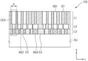
图1是示意性地示出了根据示例实施例的超颖光学器件的配置和功能的概念图。图2是图1的超颖光学器件的平面图。FIG. 1 is a conceptual diagram schematically illustrating the configuration and function of a meta-optic according to example embodiments. FIG. 2 is a plan view of the metaoptic device of FIG. 1 .
超颖光学器件100是使用具有亚波长形状尺寸的纳米结构的衍射器件,并且其具体结构被设置为相对于预定波段的入射光表示特定的目标相位延迟曲线。也就是说,目标相位延迟曲线是可以使用超颖光学器件100以预定波段的光获得(经测量或计算机模拟)的相位曲线。此处,术语“亚波长”是指小于该波段的中心波长λ0的值。The meta-
入射光L在穿过了超颖光学器件100时作为调制光Lm输出,其相位根据位置进行调制。当光入射到并穿过超颖光学器件100时,由于具有与周围材料的折射率不同的折射率的多个纳米结构NS1、NS2和NS3的布置,发生了折射率分布。由于多个纳米结构NS1、NS2和NS3的布置,在光的传播路径中相同相位的波前连接点的形式在折射率分布发生之前和之后是不同的,并且该差异被称为相位延迟。相位延迟的程度根据位置而变化,该位置是折射率分布的变量。相位延迟的程度根据与光的传播方向(Z轴方向)垂直的平面上在沿Z轴方向入射的入射光L刚好穿过超颖光学器件100后的位置处的x和y坐标而变化。如上所述,穿过超颖光学器件100的光的相位与光入射到超颖光学器件100上时的相位不同。由调制光Lm表示的目标相位延迟曲线φt表示相对于入射光L的相位的相位。目标相位延迟曲线φt表示在入射光L穿过超颖光学器件100之后的每个位置处的相位延迟,并且该相位延迟取决于入射光L的波长λ。因此,目标相位延迟曲线φt由位置和波长的函数(φt(r,λ))表示。The incident light L is output as modulated lightLm when passing through the meta-
超颖光学器件100的光学性能(例如,透镜、反射镜、光束偏转器、光束整形器等的功能)可以由目标相位延迟曲线φt确定。The optical performance of meta-optics 100 (eg, functions of lenses, mirrors, beam deflectors, beam shapers, etc.) can be determined by the target phase retardation curve φt .
超颖光学器件100包括第一层L1、第二层L2和第三层L3。第一层L1具有基于第一纳米结构NSl的结构,并用作相位延迟层,并且第二层L2和第三层L3分别具有基于第二纳米结构NS2的结构和基于第三纳米结构NS3的结构,并用作色散控制层。The meta-
第一纳米结构NS1的材料和形状分布可以被设置为使得用作相位延迟层的第一层L1表示具有与目标相位延迟曲线φt的趋势基本等同的趋势的第一相位延迟曲线,即,第一纳米结构NS1根据用于实现目标相位延迟曲线φt的位置r表现出有效折射率的变化
用作第一色散控制层的第二层L2和用作第二色散控制层的第三层L3被设置为抵消在第一层L1处发生的色散。色散与材料色散


第二纳米结构NS2的材料、形状和布置可以被设置为使得第二层L2表示具有与目标相位延迟曲线φt不同的趋势的相位延迟曲线,并且具有根据波长控制折射率色散(refractive index dispersion)的主要功能。第二层L2可以表示第二相位延迟曲线,该第二相位延迟曲线的趋势与目标相位延迟曲线φt的趋势基本相反,以抵消在第一层L1处发生的色散。即,第一层L1和第二层L2可以在根据位置的有效折射率的变化率的符号方面基本相反。例如,当第一层L1的第一纳米结构NS1的材料和形状被设置为使得有效折射率沿第一方向逐渐增加时,第二层L2的第二纳米结构NS2的材料和形状可以被设置为使得有效折射率沿第一方向逐渐减小。相反,当第一层L1的第一纳米结构NS1的材料和形状被设置为使得有效折射率沿第一方向逐渐减小时,第二层L2的第二纳米结构NS2的材料和形状可以被设置为使得有效折射率沿第一方向逐渐增加。此外,第二层L2可以采用具有高色散的材料或结构,使得根据位置的色散变化率大于第一层L1的色散变化率。The material, shape and arrangement of the second nanostructure NS2 may be set such that the second layer L2 represents a phase retardation curve having a different trend from the target phase retardation curve φt and having a wavelength-dependent refractive index dispersion main function. The second layer L2 may represent a second phase delay curve having a substantially opposite trend to that of the target phase delay curve φt to counteract the dispersion occurring at the first layer L1 . That is, the first layer L1 and the second layer L2 may be substantially opposite in sign of the change rate of the effective refractive index according to the position. For example, when the material and shape of the first nanostructure NS1 of the first layer L1 are set such that the effective refractive index gradually increases along the first direction, the material and shape of the second nanostructure NS2 of the second layer L2 may be set to The effective refractive index is gradually decreased along the first direction. Conversely, when the material and shape of the first nanostructure NS1 of the first layer L1 are set such that the effective refractive index gradually decreases along the first direction, the material and shape of the second nanostructure NS2 of the second layer L2 may be set to The effective refractive index is gradually increased along the first direction. In addition, the second layer L2 may adopt a material or structure having high dispersion, so that the dispersion change rate according to the position is greater than that of the first layer L1.
第三层L3被设置为减少高阶色散。第三层L3可以表示与第一相位延迟曲线和第二相位延迟曲线不同的相位延迟。通过修改第二层L2的材料和施加到第二层L2的布置规则中的至少一个来设置第三纳米结构NS3的材料和形状分布。第三层L3可以包括具有比第二层L2的折射率低的折射率和比第二层L2的色散低的色散的材料。即,可以采用具有比第一层L1高的色散和比第二层L2低的色散的材料作为第三层L3的材料。The third layer L3 is arranged to reduce higher order dispersion. The third layer L3 may represent a different phase delay from the first phase delay profile and the second phase delay profile. The material and shape distribution of the third nanostructures NS3 are set by modifying at least one of the material of the second layer L2 and the arrangement rule applied to the second layer L2. The third layer L3 may include a material having a refractive index lower than that of the second layer L2 and a dispersion lower than that of the second layer L2. That is, a material having higher dispersion than the first layer L1 and lower dispersion than the second layer L2 may be employed as the material of the third layer L3.
在以上描述中,第一层L1的相位延迟曲线指示相对于入射在第一纳米结构NS1上的光的相位,在光刚好穿过第一层L1的第一纳米结构NS1的位置处的相位分布。第二层L2的相位延迟曲线指示相对于入射在第二纳米结构NS2上的光的相位,在光刚好穿过第二层L2的第二纳米结构NS2后的位置处的相位分布。第三层L3的相位延迟曲线指示相对于入射在第三纳米结构NS3上的光的相位,在光刚好穿过第三层L3的第三纳米结构NS3后的位置处的相位分布。In the above description, the phase retardation curve of the first layer L1 indicates the phase distribution at the position where the light just passes through the first nanostructure NS1 of the first layer L1 with respect to the phase of the light incident on the first nanostructure NS1 . The phase retardation curve of the second layer L2 indicates the phase distribution at a position just after the light passes through the second nanostructure NS2 of the second layer L2 with respect to the phase of the light incident on the second nanostructure NS2. The phase retardation curve of the third layer L3 indicates the phase distribution at a position just after the light passes through the third nanostructure NS3 of the third layer L3 with respect to the phase of the light incident on the third nanostructure NS3.
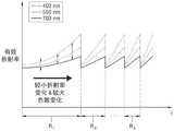
该三层结构在实现所期望的超颖光学器件100的目标相位延迟曲线φt的同时,在所期望的波段实现恒定的效率。即,该三层结构不仅在波段的中央区域处而且在周边区域处提高了所期望的光学功能的效率。波段可以包括可见光波段或近红外波段,并且其带宽可以是大约300nm或更大。在该波段处的超颖光学器件100的最小衍射效率可以是90%或更高。衍射效率是指沿所期望的方向衍射的光的能量与透射通过超颖光学器件100的光的能量的比率。该波段的带宽Δλ与中心波长λ0的比率Δλ/λ0可以是15%或更高。比率Δλ/λ0可以是40%或更高。The three-layer structure achieves constant efficiency in the desired wavelength band while achieving the desired target phase retardation curve φt of the
在实施例中,超颖光学器件100包括第一层L1、第二层L2和第三层L3,第一层L1是相位延迟层,其表现出具有与目标相位延迟曲线φt的趋势基本等同的趋势的相位延迟曲线,并且第二层L2和第三层L3是两个色散控制层,其表现出具有与目标相位延迟曲线φt不同的趋势的相位延迟曲线,并被配置为控制相位延迟层的色散,从而促进宽波段中的恒定效率。In an embodiment, the
第一层L1、第二层L2和第三层L3的位置可以彼此转换。尽管图1示出了入射光L依次穿过第一层L1、第二层L2和第三层L3,但是实施例不限于此。例如,可以设置这些层的顺序以在每一层的边界处实现尽可能小的有效折射率变化。The positions of the first layer L1, the second layer L2, and the third layer L3 may be converted from each other. Although FIG. 1 shows that the incident light L sequentially passes through the first layer L1 , the second layer L2 and the third layer L3 , the embodiment is not limited thereto. For example, the order of the layers can be arranged to achieve as little effective refractive index change as possible at the boundaries of each layer.
每层的第一纳米结构NS1、第二纳米结构NS2和第三纳米结构NS3的形状可以由第一纳米结构NS1、第二纳米结构NS2和第三纳米结构NS3的位置的函数来确定。例如,第一层L1的第一纳米结构NS1可以由第一纳米结构NS1所在的平面S1上的坐标(x,y)的函数来确定。坐标(x,y)可以由距平面S1上的与超颖光学器件100的中心轴C相交的点的距离以及对应位置的半径向量与x轴之间的角度θ的函数来确定。第二层L2的第二纳米结构NS2可以由第二纳米结构NS2所在的平面S2上的坐标(x,y)的函数来确定。坐标(x,y)可以由距平面S2上的与超颖光学器件100的中心轴C相交的点的距离以及对应位置的半径向量与x轴之间的角度θ的函数来确定。第三层L3的第三纳米结构NS3可以由第三纳米结构NS3所在的平面S3上的坐标(x,y)的函数来确定。坐标(x,y)可以由距平面S3上的与超颖光学器件100的中心轴C相交的点的距离以及对应位置的半径向量与x轴之间的角度θ的函数来确定。第一层L1的第一纳米结构NS1、第二层L2的第二纳米结构NS2和第三层L3的第三纳米结构NS3中的每一个可以由仅取决于距其中心的距离的极性对称函数来确定。The shape of the first nanostructure NS1, the second nanostructure NS2 and the third nanostructure NS3 of each layer may be determined as a function of the position of the first nanostructure NS1, the second nanostructure NS2 and the third nanostructure NS3. For example, the first nanostructure NS1 of the first layer L1 may be determined by a function of coordinates (x, y) on the plane S1 on which the first nanostructure NS1 is located. The coordinates (x, y) can be determined as a function of the distance from the point on the plane S1 that intersects the central axis C of the meta-
第一纳米结构NS1、第二纳米结构NS2和第三纳米结构NS3中的每一个可以基于矩形坐标二维地布置,以六边形点阵形式布置,或者相对于极坐标在径向或周向上二维地布置。Each of the first nanostructures NS1 , the second nanostructures NS2 and the third nanostructures NS3 may be arranged two-dimensionally based on rectangular coordinates, in a hexagonal lattice, or radially or circumferentially with respect to polar coordinates Arranged two-dimensionally.
在实施例中,第一纳米结构NS1、第二纳米结构NS2和第三纳米结构NS3的形状和布置可以被设置为在远离第一纳米结构NS1、第二纳米结构NS2和第三纳米结构NS3所在的平面S1、S2和S3上定义的中心的径向上实现相位延迟曲线和有效折射率的变化。In an embodiment, the shape and arrangement of the first nanostructure NS1 , the second nanostructure NS2 and the third nanostructure NS3 may be arranged to be remote from where the first nanostructure NS1 , the second nanostructure NS2 and the third nanostructure NS3 are located The phase retardation curve and the variation of the effective refractive index are realized radially from the center defined on the planes S1, S2 and S3.
第一纳米结构NS1、第二纳米结构NS2和第三纳米结构NS3的形状可以遵循特定规则,并且根据该规则划分第一层L1、第二层L2和第三层L3的每个区域。超颖光学器件100的区域可以被划分为中央圆形区域R1和围绕该中央圆形区域R1的多个环形区域R2、..、RN,如图2所示。每一层的相同区域中的纳米结构NS1、NS2和NS3可以根据相同的规则布置。The shapes of the first nanostructure NS1 , the second nanostructure NS2 and the third nanostructure NS3 may follow a specific rule, and each area of the first layer L1 , the second layer L2 and the third layer L3 is divided according to the rule. The area of the meta-optic 100 may be divided into a central circular area R1 and a plurality of annular areas R2 , . . . , RN surrounding the central circular area R1 , as shown in FIG. 2 . The nanostructures NS1 , NS2 and NS3 in the same area of each layer can be arranged according to the same rules.
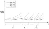
区域R1、...、Rk、...、RN是指示特定范围内的相位延迟的相位调制区域,并且第二区域R2至第N区域RN的相位调制范围可以相同。相位调制范围可以是2π弧度。第一区域R1的相位调制范围可以是2π弧度或更小,但是第一区域R1至第N区域RN通常可以被统称为2π区。TheregionsR1, . . . ,Rk , . The phase modulation range can be 2π radians. The phase modulation range of the first region R1 may be 2π radians or less, but the first region R1 to theNth region RN may generally be collectively referred to as a 2π region.
这些区域的功能和总数N或宽度WR1、...、WRk、...、WRN可以是超颖光学器件100的性能的主要变量。如上所述,超颖光学器件100的第一层L1是负责相位的层,并且表现出具有与目标相位曲线基本相似的趋势的相位曲线。根据第一层L1表现出的相位曲线来设置超颖光学器件100的光学功能,并且第二层L2和第三层L3主要有助于超颖光学器件100的光学功能的效率。The function and total number N of these regions orwidths WR1 , . . . ,WRk , . As described above, the first layer L1 of the
第一层L1可以包括与多个相位调制区域R1、...、Rk、...、RN之间的边界相邻的部分FR,该部分FR不包括第一纳米结构NS1。部分FR可以被表示为具有100%的填充因子的区域。部分FR可以设置在多个相位调制区域R1、...、Rk、...、RN的一部分中,并且可以设置多个部分FR。部分FR的宽度WFR与相应的相位调制区域的宽度WRK的比率可以为5%或更大。The first layer L1 may include a portion FR adjacent to the boundary between the plurality of phase modulation regions R1 , . . . , Rk , . . ,RN , the portion FR not including the first nanostructure NS1 . A partial FR can be represented as a region with a fill factor of 100%. The partial FR may be provided in a part of the plurality of phase modulation regions R1 , . . . , Rk , . . ,RN , and a plurality of the partial FR may be provided. The ratio of the width WFR of the partial FR to the widthWRK of the corresponding phase modulation region may be 5% or more.
部分FR的位置可以是相位调制区域的开始或结束位置。例如,部分FR的位置可以根据第一层L1的第一纳米结构NS1具有比周围材料的折射率低的折射率还是比周围材料的折射率高的折射率而变化。部分FR可以被设置为减少可能在每个相位调制区域的端部(即,每个相位调制区域的与另一相位调制区域相邻的一部分)出现的相位曲线的不连续性。The position of the partial FR may be the start or end position of the phase modulation region. For example, the position of the portion FR may vary depending on whether the first nanostructure NS1 of the first layer L1 has a lower refractive index than that of the surrounding material or a higher refractive index than that of the surrounding material. The partial FR may be set to reduce discontinuities in the phase curve that may occur at the ends of each phase modulation region (ie, a portion of each phase modulation region adjacent to another phase modulation region).
为了允许超颖光学器件100用作镜头,可以设置区域内的规则,使得每个区域的宽度不同,并且每个区域中的入射光的衍射方向略有不同。区域的数量与屈光力的程度(例如,绝对值)有关,并且可以根据区域内的规则来确定屈光力的符号。例如,可以根据用于在径向上减小每个区域中的第一纳米结构NS1的尺寸的布置规则来实现正屈光力,并且可以根据用于在径向上增大每个区域中的第一纳米结构NS1的尺寸的布置规则来实现负屈光力。To allow meta-
为了允许超颖光学器件100用作光束偏转器,区域内的规则可以被设置为使得第一层L1的区域R1、R2、...、RN的宽度WR1、...、WRk、...、WRN可以相同,并且每个区域中的入射光L可以沿特定方向衍射。In order to allow the meta-
超颖光学器件100可以用作具有根据位置的分布的光束整形器、以及透镜或光束偏转器。The meta-
第一纳米结构NS1、第二纳米结构NS2和第三纳米结构NS3均由具有与周围材料的折射率不同的折射率的材料形成。例如,该材料的折射率可以比周围材料的折射率大0.2或更多或者小0.2或更多。折射率差可以为大约0.2或更大,或者为大约0.5或更大。第一纳米结构NS1、第二纳米结构NS2和第三纳米结构NS3中的一部分可以具有比周围材料的折射率高的折射率,而其他部分可以具有比周围材料的折射率低的折射率。The first nanostructure NS1 , the second nanostructure NS2 and the third nanostructure NS3 are each formed of a material having a refractive index different from that of the surrounding material. For example, the refractive index of the material may be 0.2 or more or 0.2 or more less than the refractive index of the surrounding material. The refractive index difference may be about 0.2 or more, or about 0.5 or more. A portion of the first nanostructure NS1 , the second nanostructure NS2 and the third nanostructure NS3 may have a refractive index higher than that of the surrounding material, and other portions may have a refractive index lower than that of the surrounding material.
当第一纳米结构NS1、第二纳米结构NS2和第三纳米结构NS3由具有比周围材料的折射率高的折射率的材料形成时,第一纳米结构NS1、第二纳米结构NS2和第三纳米结构NS3可以包括c-Si、p-Si、a-Si或III-V化合物半导体(GaAs、GaP、GaN等)中的至少一种,并且具有较低折射率的周围材料可以包括聚合物材料(例如,SU-8或PMMA)、SiO2或SOG。When the first nanostructure NS1, the second nanostructure NS2 and the third nanostructure NS3 are formed of a material having a higher refractive index than that of the surrounding material, the first nanostructure NS1, the second nanostructure NS2 and the third nanostructure Structure NS3 may include at least one of c-Si, p-Si, a-Si, or III-V compound semiconductors (GaAs, GaP, GaN, etc.), and surrounding materials with lower refractive indices may include polymeric materials ( For example, SU-8 or PMMA),SiO2 or SOG.
当第一纳米结构NS1、第二纳米结构NS2和第三纳米结构NS3由具有比周围材料的折射率低的折射率的材料形成时,第一纳米结构NS1、第二纳米结构NS2和第三纳米结构NS3可以包括SiO2或空气,并且具有较高折射率的周围材料可以包括c-Si、p-Si、a-Si或III-V族化合物半导体(GaAs、GaP、GaN等)中的至少一种或其组合。When the first nanostructure NS1 , the second nanostructure NS2 and the third nanostructure NS3 are formed of a material having a refractive index lower than that of the surrounding material, the first nanostructure NS1 , the second nanostructure NS2 and the third nanostructure The structure NS3 may includeSiO2 or air, and the surrounding material having a higher refractive index may include at least one of c-Si, p-Si, a-Si or III-V compound semiconductors (GaAs, GaP, GaN, etc.) species or combinations thereof.
图3是示出了图1的超颖光学器件100的相位延迟层的根据波长和位置的有效折射率和色散的曲线图。图4是示出了图1的超颖光学器件100的第一色散控制层的根据波长和位置的有效折射率和色散的曲线图。FIG. 3 is a graph showing the effective refractive index and dispersion according to wavelength and position of the phase retardation layer of the
有效折射率是假设超颖光学器件100的单位组件可以被视为均匀介质的概念。当具有不同折射率的介质包括在单位组件中时,有效折射率的概念可以暗示不同介质的分布。The effective refractive index is a concept that assumes that the unit component of the
折射率色散是指折射率根据波长而变化的程度
一起参考图3和图4,相位延迟层和第一色散控制层在有效折射率在第一方向上的变化趋势方面是基本相反的。在曲线图中,在径向R上示出了有效折射率的变化趋势。相位延迟层可以在根据位置的有效折射率的变化方面具有与目标相位延迟曲线基本相似的趋势。Referring to FIGS. 3 and 4 together, the phase retardation layer and the first dispersion control layer are substantially opposite in changing trends of the effective refractive index in the first direction. In the graph, the variation trend of the effective refractive index in the radial direction R is shown. The phase retardation layer may have a substantially similar tendency to the target phase retardation curve in the change of the effective refractive index according to the position.
根据有效折射率的变化趋势,由相位延迟层表示的相位延迟曲线和目标相位延迟曲线在根据位置的变化率的符号方面是基本相似的,并且由第一色散控制层表示的相位延迟曲线和目标相位延迟曲线可以在根据位置的变化率的符号方面是基本相反的。换句话说,由相位延迟层表示的相位延迟曲线和由第一色散控制层表示的相位延迟曲线可以在根据位置的变化率的符号方面是基本相反的。According to the variation trend of the effective refractive index, the phase retardation curve represented by the phase retardation layer and the target phase retardation curve are substantially similar in the sign of the rate of change according to the position, and the phase retardation curve represented by the first dispersion control layer and the target The phase delay curves may be substantially opposite in sign of the rate of change as a function of position. In other words, the phase retardation curve represented by the phase retardation layer and the phase retardation curve represented by the first dispersion control layer may be substantially opposite in sign of the rate of change according to the position.
相位延迟层和第一色散控制层可以在根据位置的色散变化率的比率
在相位延迟层的情况下,如图3的曲线图所示的根据位置的有效折射率的变化率大于如图4所示的第一色散控制层中的根据位置的有效折射率的变化率。相反,相位延迟层在色散度(即,根据波长的有效折射率的变化率)方面小于第一色散控制层。因此,第一色散控制层的根据位置的色散变化率大于相位延迟层的色散变化率。为此,作为第一色散控制层的第二层L2的材料的色散可以高于作为相位延迟层的第一层L1的材料的色散。例如,Si、TiO2等可以被用作具有高色散的材料,并且SiO2、Si3N4等可以被用作具有低色散的材料。然而,以上材料仅是示例,并且实施例不限于此。根据位置的色散变化率与有效折射率变化率的比率与介质的色散、折射率、形状分布等密切相关。例如,当纳米结构的材料的折射率小于周围材料的折射率时根据位置的色散变化率小于当纳米结构的材料的折射率大于周围材料的折射率时的色散变化率。因此,可以通过组合与示例的材料和形状不同的材料和形状来调节根据位置的色散变化率。In the case of the phase retardation layer, the change rate of the effective refractive index according to the position as shown in the graph of FIG. 3 is larger than the change rate of the effective refractive index according to the position in the first dispersion control layer as shown in FIG. 4 . In contrast, the phase retardation layer is smaller than the first dispersion control layer in the degree of dispersion (ie, the rate of change of the effective refractive index according to wavelength). Therefore, the dispersion change rate according to the position of the first dispersion control layer is larger than the dispersion change rate of the phase retardation layer. For this reason, the dispersion of the material of the second layer L2 as the first dispersion control layer may be higher than that of the material of the first layer L1 as the phase retardation layer. For example, Si, TiO2 or the like can be used as a material with high dispersion, and SiO2 , Si3 N4 or the like can be used as a material with low dispersion. However, the above materials are only examples, and the embodiments are not limited thereto. The ratio of the dispersion change rate according to the position to the effective refractive index change rate is closely related to the dispersion, refractive index, shape distribution, etc. of the medium. For example, the rate of dispersion change according to position when the refractive index of the nanostructured material is smaller than that of the surrounding material is smaller than that when the refractive index of the nanostructured material is greater than that of the surrounding material. Therefore, the dispersion change rate according to the position can be adjusted by combining materials and shapes different from those exemplified.
图3和图4的曲线图示出了根据位置的有效折射率的变化趋势和根据位置的色散变化率在两个层中不同的示例,但是实施例不限于此。尽管示出了在区域R1、R2、...、Rk上的所有位置中都显示出上述趋势,但是上述趋势应被理解为意指在大多数区域中出现的普遍趋势。例如,在第一层L1和第二层L2的一些区域中可以出现有效折射率的基本相似的变化趋势。The graphs of FIGS. 3 and 4 show an example in which the variation trend of the effective refractive index according to the position and the variation rate of the dispersion according to the position are different in the two layers, but the embodiment is not limited thereto. Although it is shown that the above trend is shown in all positions on the regions R1 , R2 , . . . , Rk , the above trend should be understood to mean a general trend that occurs in most regions. For example, substantially similar variation trends in the effective refractive index may occur in some regions of the first layer L1 and the second layer L2.
图5A至图5C是分别示出了图1的超颖光学器件的相位延迟层的相位延迟曲线、图1的超颖光学器件的第一色散控制层的相位延迟曲线和图1的超颖光学器件的相位延迟曲线的曲线图。5A to 5C are diagrams showing the phase retardation curve of the phase retardation layer of the metaoptic device of FIG. 1 , the phase retardation curve of the first dispersion control layer of the metaoptic device of FIG. 1 , and the metaoptics of FIG. 1 , respectively. Graph of the phase delay curve of the device.
根据图3的第一层L1的有效折射率的曲线图,第一层L1的相位延迟曲线如图5A所示。根据图4的第二层L2的有效折射率的曲线图,第二层L2的相位延迟曲线如图5B所示。根据第一层L1、第二层L2和第三层L3,超颖光学器件的相位延迟曲线如图5C所示。According to the graph of the effective refractive index of the first layer L1 in FIG. 3 , the phase retardation curve of the first layer L1 is shown in FIG. 5A . According to the graph of the effective refractive index of the second layer L2 in FIG. 4 , the phase retardation curve of the second layer L2 is shown in FIG. 5B . According to the first layer L1, the second layer L2 and the third layer L3, the phase retardation curve of the meta optical device is shown in FIG. 5C.
超颖光学器件100包括表现出如图3和图5A的曲线图所示的特性的第一层L1、表现出如图4和图5B的曲线图所示的特性的第二层L2和用于抵消高阶色散的第三层L3的组合,该超颖光学器件100可以显示出根据位置几乎不连续并且无论波长如何都几乎相同的相位延迟曲线。The meta-
在图5C的曲线图中,相位延迟曲线以恒定值偏移,但是对于三个波长具有相同的形状。这对应于在波段中色散为0的情况。这是理论上的示例,但是可以通过控制色散控制层以及第一和第二色散控制层的具体形状和材料,将色散在所期望的波段中最小化。In the graph of Figure 5C, the phase retardation curve is shifted by a constant value, but has the same shape for the three wavelengths. This corresponds to the case where the dispersion is 0 in the band. This is a theoretical example, but dispersion can be minimized in the desired wavelength band by controlling the specific shape and material of the dispersion control layer and the first and second dispersion control layers.
下面将描述从中得出用于宽波段中所期望的相位调制的上述三层结构的理论。The theory from which the above-described three-layer structure for desired phase modulation in a broad band is derived will be described below.
在理想情况下,可以将泰勒展开应用于具有n个连续参数{Pi}={P1,P2,...,Pn}的超颖结构(亚波长纳米结构)相对于角频率ω的相位调制的程度,如下所示:In an ideal case, the Taylor expansion can be applied to metastructures (subwavelength nanostructures) with n continuous parameters {Pi }={P1 , P2 , . . . , Pn } with respect to the angular frequency ω The degree of phase modulation of , as follows:
φ(Pi;ω)=φ0+(ω-ω0)φ1+(ω-ω0)2φ2+…。φ(Pi ; ω)=φ0 +(ω-ω0 )φ1 +(ω-ω0 )2 φ2 +….
当相变范围为2π或更大并且具有不依赖于波长的特性时,宽带衍射效率可以为100%。即,When the phase transition range is 2π or more and has wavelength-independent characteristics, the broadband diffraction efficiency can be 100%. which is,
φ1(Pi)=const,φ2(Pi)=const,…,φk(Pi)=const。φ1 (Pi )=const, φ2 (Pi )=const, . . . , φk (Pi )=const.
当考虑经受k个约束的表面S时,存在连续参数的变化路径L:[0,1]→S,并且When considering a surface S subject to k constraints, there is a changing path L of continuous parameters: [0, 1] → S, and
φ(L[1])-φ(L[0])=φ0({Pi}final)-φ0({Pi}initial)≥2πφ(L[1])-φ(L[0])=φ0 ({Pi }final )-φ0 ({Pi }initial )≥2π
被满足。在这种情况下,当在变化路径L中改变参数以满足φ0(Pi)=mod(φ0,target,2π)+φ(L[0])以便实现相位调制曲线
实际上,即使实现了具有不依赖于波长的特性的表面,当优化连续参数的变化路径L以最小化色散变化率时,也可以获得高宽带衍射效率。这可以表示如下:In fact, even if a surface with wavelength-independent properties is realized, high broadband diffraction efficiency can be obtained when the variation path L of the continuous parameter is optimized to minimize the dispersion variation rate. This can be expressed as follows:
具有n个参数{Pi}={P1,P2,...,Pn}的超颖结构的相位偏差φcenter(ω)=φ0,center+(ω-ω0)φ1.center+(ω-ω0)φ2,center+…Phase deviationsofmetastructures with n parameters{ Pi }={P1 , P2 ,... ,Pn }center + (ω-ω0 )φ2, center +…
可以针对以下集中式色散进行评估:It can be evaluated for the following concentrated dispersions:

此处,可以修改评估方法。w(ω)表示根据每个频率的权重函数。存在完全连续的路径L:φ0,target→{Pi},用于根据给定的φcenter(ω)最大化评估指数FoM。即,Here, the evaluation method can be modified. w(ω) represents a weight function according to each frequency. There exists a perfectly continuous path L: φ0, target → {Pi } for maximizing the evaluation index FoM according to a given φcenter (ω). which is,

此处,φ0,target是[0,2π]的元素。然而,集中式色散也可以被优化。Here, φ0,target is an element of [0, 2π]. However, concentrated dispersion can also be optimized.

因此,当获得用于最大化所优化的集中式色散

(此处,φ0,target是[0,2π]的元素),(here, φ0, target is an element of [0, 2π]),
相位调制曲线


此处,可用的参数空间轴包括超颖结构在多层结构的每一层处的尺寸或布置规则等。Here, the available parameter space axes include the size or arrangement rules of the metastructure at each layer of the multilayer structure, and the like.
与理想情况相比,使用当前方法进行表观维度分析比较困难,然而,增加问题的自由度会扩大最佳路径的选择范围,从而导致更好的衍射效率和选择,使得高阶项的色散变得相似。Apparent dimensional analysis using current methods is more difficult compared to the ideal case, however, increasing the degree of freedom of the problem expands the choice of optimal paths, leading to better diffraction efficiency and selection, making the dispersion of higher-order terms more variable. be similar.
对于有效地抵消高阶项的多级结构,最好使各级的色散特性不同。当由于最佳路径L*:φ0,target→{Pi}的微小变化而引起的相位差不依赖于波长时,可以获得最大性能。即,相对于根据最佳路径L*的微小变化dPi,For a multi-level structure that effectively cancels the higher-order terms, it is preferable to make the dispersion characteristics of the stages different. Maximum performance can be obtained when the phase difference due to small changes in the optimal path L* : φ0, target → {Pi } does not depend on the wavelength. That is, with respect to the small change dPi according to the optimal path L* ,

被满足,并且在这种情况下,对每个参数的变化有不同的贡献。is satisfied, and in this case, has a different contribution to the variation of each parameter.
即,当That is, when

平行于微小变化的单位向量


为了将k个约束增加到(n-1)个理想条件,矩阵


可以用于确定最佳路径中微小变化的方向。即,存在最佳路径。在这种情况下,k=n-1。对于平凡(trivial)情况,即,当各级的色散特性相似或相同时的情况,逆是单数,并且因此,通常,k≤n-1。Can be used to determine the direction of small changes in the optimal path. That is, there is an optimal path. In this case, k=n-1. For the trivial case, ie, when the dispersion characteristics of the stages are similar or the same, the inverse is singular, and thus, in general, k≤n-1.
每一层的色散可以由超颖结构的材料值、形状和布置确定。因此,超颖结构的材料值、形状和布置可以是宽带高效多级结构的元素,因为每个色散特性在对其进行一个或多个修改时发生变化。The dispersion of each layer can be determined by the material value, shape and arrangement of the metastructure. Thus, the material values, shapes, and arrangements of metastructures can be elements of broadband efficient multilevel structures, as each dispersive property changes when one or more modifications are made to it.
可以将每一层的高度变化视为对矩阵的秩没有很大影响的元素,因为期望在具有高纵横比的超颖结构的情况下可以获得与高度成比例的相位差。The height variation of each layer can be regarded as an element that does not have a great influence on the rank of the matrix, since it is expected that a phase difference proportional to the height can be obtained in the case of metastructures with high aspect ratios.

为了使高度最小化,需要对多级结构的材料、形状和布置方法进行综合优化,并且该综合优化可以直观地描述如下。In order to minimize the height, a comprehensive optimization of the materials, shapes, and arrangement methods of the multilevel structure is required, and this comprehensive optimization can be intuitively described as follows.
通过选择具有低色散但是能够在很大程度上显著改变相位的结构来实现一级等效结构以满足2π的相变范围。除了一级等效结构,还配置两级等效结构来抵消色散。在两级等效结构中,相对于相变范围的色散变化范围被设置为尽可能高以使高度最小化。第二级等效结构被配置为主要补偿一次色散。在三级等效结构中,相对于相变范围的二次色散变化范围被设置为很高以主要补偿二次色散。The first-order equivalent structure is achieved to satisfy the phase transition range of 2π by choosing a structure that has low dispersion but is capable of significantly changing the phase to a large extent. In addition to the one-level equivalent structure, a two-level equivalent structure is also configured to cancel the dispersion. In the two-stage equivalent structure, the dispersion variation range with respect to the phase transition range is set as high as possible to minimize the height. The second-level equivalent structure is configured to primarily compensate for primary dispersion. In the three-level equivalent structure, the secondary dispersion variation range with respect to the phase transition range is set high to mainly compensate the secondary dispersion.
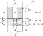
图6是示出了在图1的超颖光学器件中可以采用的单位组件的特定形状和折射率布置的截面图。FIG. 6 is a cross-sectional view illustrating a specific shape and refractive index arrangement of unit components that may be employed in the metaoptic device of FIG. 1 .
可以通过根据其位置改变详细尺寸来在超颖光学器件100中重复地设置单位组件UE1。The unit component UE1 can be repeatedly arranged in the meta-
第一层L1包括第一纳米结构NS1和围绕该第一纳米结构NS1的第一周围材料E1。第一纳米结构NS1的折射率n1可以低于第一周围材料E1的折射率n2。第一纳米结构NS1可以是空的空间(即,空气),并且可以具有如下形状,在该形状中,以特定的宽度和深度雕刻了第一周围材料E1。在下文中,当纳米结构被描述为具有比周围材料的折射率低的折射率时,应理解为包括纳米结构包含空气的情况,即,纳米结构具有雕刻的空孔形状的情况。The first layer L1 includes a first nanostructure NS1 and a first surrounding material E1 surrounding the first nanostructure NS1. The refractive index n1 of the first nanostructure NS1 may be lower than the refractive index n2 of the first surrounding material E1. The first nanostructure NS1 may be an empty space (ie, air), and may have a shape in which the first surrounding material E1 is engraved with a specific width and depth. In the following, when a nanostructure is described as having a lower refractive index than that of the surrounding material, it should be understood to include the case where the nanostructure contains air, ie the case where the nanostructure has an engraved void shape.
第二层L2包括第二纳米结构NS2和围绕该第二纳米结构NS2的第二周围材料E2。第二纳米结构NS2可以由具有比第二周围材料E2的折射率n4高的折射率n3的材料形成。第三层L3包括第三纳米结构NS3和围绕该第三纳米结构NS3的第三周围材料E3。第三纳米结构NS3可以由具有比第三周围材料E3的折射率n6高的折射率n5的材料形成。第三纳米结构NS3的折射率n5可以低于第二纳米结构NS2的折射率n3。The second layer L2 includes a second nanostructure NS2 and a second surrounding material E2 surrounding the second nanostructure NS2. The second nanostructure NS2 may be formed of a material having a higher refractive index n3 than the refractive index n4 of the second surrounding material E2. The third layer L3 includes a third nanostructure NS3 and a third surrounding material E3 surrounding the third nanostructure NS3. The third nanostructure NS3 may be formed of a material having a higher refractive index n5 than the refractive index n6 of the third surrounding material E3. The refractive index n5 of the third nanostructure NS3 may be lower than the refractive index n3 of the second nanostructure NS2.
第二周围材料E2可以延伸为覆盖第二纳米结构NS2以在第一纳米结构NS1和第二纳米结构NS2之间形成间隙s2,并且第三周围材料E3可以延伸为覆盖第三纳米结构NS3以在第二纳米结构NS2和第三纳米结构NS3之间形成间隙s1。间隙s1和s2是示例,并且可以为零。The second surrounding material E2 may extend to cover the second nanostructure NS2 to form a gap s2 between the first nanostructure NS1 and the second nanostructure NS2, and the third surrounding material E3 may extend to cover the third nanostructure NS3 to A gap s1 is formed between the second nanostructure NS2 and the third nanostructure NS3. The gaps s1 and s2 are examples and may be zero.
第一纳米结构NS1、第二纳米结构NS2和第三纳米结构NS3可以均具有亚波长尺寸。第一纳米结构NS1、第二纳米结构NS2和第三纳米结构NS3各自的宽度w1、w2和w3可以是亚波长,并且单位组件UE1的间距P也可以是亚波长。The first nanostructure NS1 , the second nanostructure NS2 and the third nanostructure NS3 may all have sub-wavelength dimensions. The respective widths w1 , w2 and w3 of the first nanostructure NS1 , the second nanostructure NS2 and the third nanostructure NS3 may be subwavelengths, and the pitch P of the unit component UE1 may also be subwavelengths.
第一纳米结构NS1可以具有大于1的纵横比,以避免其中的光学共振。即,h1/w1可以大于1,并且可以大于例如2。第一纳米结构NS1相对于波段的中心波长λ0的高度可以在2λ0至5λ0的范围内。The first nanostructure NS1 may have an aspect ratio greater than 1 to avoid optical resonance therein. That is, h1/w1 may be greater than 1, and may be greater than 2, for example. The height of the first nanostructure NS1 with respect to the center wavelength λ0 of the band may be in the range of 2λ0 to 5λ0 .
第二纳米结构NS2的高度h2和第三纳米结构NS3的高度h3可以相对于波段的中心波长λ0均在0.5λ0至2λ0的范围内。The height h2 of the second nanostructure NS2 and the height h3 of the third nanostructure NS3 may both be in the range of 0.5λ0 to 2λ0 with respect to the center wavelength λ0 of the band.
还可以设置用于支撑第一层L1、第二层L2和第三层L3的基板SU。基板SU可以相对于超颖光学器件100的工作波段的光具有透明性质,并且可以由玻璃(熔融二氧化硅、BK7等)、石英、聚合物(PMMA、BK7等)或另一种透明塑料形成。基板SU的折射率可以等于或小于第三周围材料E3的折射率n6。如图6所示,可以在基板SU上设置第三层L3,然后可以在第三层L3上设置第二层L2和第一层L1。这种布置旨在尽可能小地减小相邻层之间的有效折射率的变化,并且可以根据折射率n1和n2而改变为第一层L1、第三层L3和第二层L2的顺序。A substrate SU for supporting the first layer L1, the second layer L2 and the third layer L3 may also be provided. The substrate SU may have transparent properties with respect to light in the operating wavelength band of the meta-
图7是示出了根据图6的单位组件UE1的大小变化的、关于相位的计算机模拟结果的曲线图。图8是示出了根据图7的计算机模拟结果的、关于超颖光学器件的透射率和效率的计算机模拟结果的曲线图。FIG. 7 is a graph showing a computer simulation result with respect to the phase according to the size change of the unit component UE1 of FIG. 6 . FIG. 8 is a graph showing computer simulation results regarding transmittance and efficiency of a meta-optic according to the computer simulation results of FIG. 7 .
在图7的计算机模拟中,h1为3μm,并且h2和h3均为0.8μm。对于具有550nm的波长的光,第一纳米结构NS1的折射率n1为1.4599,第一周围材料E1的折射率n2为2.2706,第二纳米结构NS2的折射率n3为2.2706,第二周围材料E2的折射率n4为1.4599,第三纳米结构NS3的折射率n5为1.7896,并且第三周围材料E3的折射率n6为1.4599。In the computer simulation of Figure 7, h1 is 3 μm, and both h2 and h3 are 0.8 μm. For light with a wavelength of 550 nm, the refractive index n1 of the first nanostructure NS1 is 1.4599, the refractive index n2 of the first surrounding material E1 is 2.2706, the refractive index n3 of the second nanostructure NS2 is 2.2706, and the refractive index n3 of the second surrounding material E2 The refractive index n4 is 1.4599, the refractive index n5 of the third nanostructure NS3 is 1.7896, and the refractive index n6 of the third surrounding material E3 is 1.4599.
参考图7,可以根据每个位置处所需的相位延迟值适当地设置包括在单位组件UE1中的具体形状,即,第一纳米结构NS1的宽度w1、第二纳米结构NS2的宽度w2和第三纳米结构NS3的宽度w3,以实现所期望的光学性能。Referring to FIG. 7, specific shapes included in the unit component UE1, ie, the width w1 of the first nanostructure NS1, the width w2 of the second nanostructure NS2, and the The width w3 of the three-nanostructure NS3 to achieve the desired optical properties.
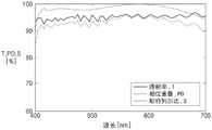
在图8的曲线图中,“相位重叠”和“斯特列尔比(Strehl ratio)”分别表示与衍射效率相对应的概念和与聚光效率相对应的概念。三个特征(即,透射率T、衍射效率PO和聚光效率S)通常是恒定的,并且在400至700nm的波段中良好。特别地,衍射效率PO为97%或更高的带宽为大约250nm。衍射效率PO为90%或更高的300nm的带宽与550nm的中心波长的比率为54%或更大。In the graph of FIG. 8 , “phase overlap” and “Strehl ratio” represent a concept corresponding to diffraction efficiency and a concept corresponding to light gathering efficiency, respectively. Three characteristics (ie, transmittance T, diffraction efficiency PO, and light-gathering efficiency S) are generally constant, and are good in the wavelength band of 400 to 700 nm. In particular, the bandwidth at which the diffraction efficiency PO is 97% or higher is about 250 nm. The ratio of the bandwidth of 300 nm to the center wavelength of 550 nm at which the diffraction efficiency PO is 90% or more is 54% or more.
图9是示出了比较例的超颖光学器件的透射率和效率的计算机模拟的曲线图。FIG. 9 is a graph showing a computer simulation of the transmittance and efficiency of the meta-optic of the comparative example.
该比较例的超颖光学器件是实施为单层结构的示例。参照该曲线图,透射率T、衍射效率PO和聚光效率S在400至700nm的波段的中央区域处较高,但是在周边区域中非常低。可以将由左边圆圈表示的减量评估为由于意外方向上的衍射而导致的减量,并且可以将由右边圆圈表示的减量评估为由于缺乏相位而导致的减量。The metaoptic device of this comparative example is an example implemented as a single-layer structure. Referring to the graph, the transmittance T, the diffraction efficiency PO, and the condensing efficiency S are high in the central region of the wavelength band of 400 to 700 nm, but very low in the peripheral region. The decrement represented by the circle on the left can be evaluated as the decrement due to diffraction in unexpected directions, and the decrement represented by the circle on the right can be evaluated as the decrement due to the lack of phase.
图10是示出了根据实施例的超颖光学器件的结构的示意性截面图。FIG. 10 is a schematic cross-sectional view showing the structure of a meta-optic according to an embodiment.
超颖光学器件101具有应用了图6的单位组件UE1的结构,其中单位组件UE1用作透镜。然而,为了便于说明省略了s1和s2,并且可以设置适当的间隙。在以下实施例中,示出了在每个不同层的纳米结构之间不存在间隙,但是这是为了便于说明的示例,并且可以形成特定间隙。The meta-
在第一层L1上,具有比第一周围材料E1的折射率低的折射率的第一纳米结构NS1沿使其宽度减小的方向布置。在第二层L2上,具有比第二周围材料E2的折射率高的折射率的第二纳米结构NS2沿使其宽度减小的方向布置。该方向可以是图2所示的径向R。第一层L1和第二层L2在远离超颖光学器件101的中心的方向上显示出基本相似的宽度变化趋势,并且因此在相位调制趋势的符号方面是相反的。第二层L2在折射率的符号方面显示出与第一层L1不同的折射率变化趋势,并且可以主要补偿在第一层L1中出现的一次色散。On the first layer L1, the first nanostructures NS1 having a lower refractive index than that of the first surrounding material E1 are arranged in a direction in which the width thereof is reduced. On the second layer L2, the second nanostructures NS2 having a higher refractive index than that of the second surrounding material E2 are arranged in a direction in which the width thereof is reduced. This direction may be the radial direction R shown in FIG. 2 . The first layer L1 and the second layer L2 show substantially similar width variation trends in the direction away from the center of the meta-
第三层L3包括具有比第三周围材料E3的折射率高的折射率的第三纳米结构NS3。第三纳米结构NS3可以由具有比第二纳米结构NS2的折射率低的折射率和比第二纳米结构NS2的色散低的色散的材料形成。第三层L3可以主要补偿高阶色散。The third layer L3 includes a third nanostructure NS3 having a higher refractive index than that of the third surrounding material E3. The third nanostructure NS3 may be formed of a material having a lower refractive index than that of the second nanostructure NS2 and a lower dispersion than that of the second nanostructure NS2. The third layer L3 can mainly compensate for higher-order dispersion.
下面将描述根据各种修改示例的超颖光学器件。现在将着重于与先前实施例的超颖光学器件的差异来描述超颖光学设备。Meta-optics according to various modified examples will be described below. The meta-optic device will now be described focusing on the differences from the meta-optic device of the previous embodiment.
图11A是示出了根据另一实施例的超颖光学器件的结构的示意性截面图。图11B是示出了图11A的超颖光学器件的单位组件的折射率布置的截面图。FIG. 11A is a schematic cross-sectional view showing the structure of a meta-optic according to another embodiment. FIG. 11B is a cross-sectional view showing the refractive index arrangement of the unit components of the meta-optic of FIG. 11A .
超颖光学器件102的单位组件UE2与图10的超颖光学器件101在第三层L3的折射率布置方面不同,并且因此,第三层L3、第一层L1和第二层L2被依次布置在基板SU上。The unit component UE2 of the meta-
在第三层L3上,第三纳米结构NS3的折射率n5小于第三周围材料E3的折射率n6。因此,可以将第一层L1设置在第三层L3上,并且可以将第二层L2设置在第一层L1上,以尽可能小地减小相邻层之间的折射率的变化率。On the third layer L3, the refractive index n5 of the third nanostructure NS3 is smaller than the refractive index n6 of the third surrounding material E3. Therefore, the first layer L1 may be provided on the third layer L3, and the second layer L2 may be provided on the first layer L1 to reduce the rate of change in refractive index between adjacent layers as small as possible.
图12A是示出了根据另一实施例的超颖光学器件的结构的示意性截面图。图12B是示出了图12A的超颖光学器件的单位组件的折射率布置的截面图。FIG. 12A is a schematic cross-sectional view showing the structure of a meta-optic according to another embodiment. 12B is a cross-sectional view showing the refractive index arrangement of the unit components of the metaoptic of FIG. 12A.
超颖光学器件103的单位组件UE3与图10的超颖光学器件101的不同之处在于,第二纳米结构NS2的折射率n3被改变为低于第二周围材料E2的折射率n4,从而改变第二纳米结构NS2的宽度w2的变化趋势。第二纳米结构NS2的根据位置的宽度w2被设置为与第一纳米结构NS1的宽度w1的变化趋势基本相反。因此,第一层L1和第二层L2在根据位置的有效折射率的变化方面是基本相反的,并且在根据位置的相位调制的变化方面是基本相反的。The unit component UE3 of the meta-
图13A是示出了根据另一实施例的超颖光学器件的结构的示意性截面图。图13B是示出了图13A的超颖光学器件的单位组件的折射率布置的截面图。FIG. 13A is a schematic cross-sectional view showing the structure of a meta-optic according to another embodiment. 13B is a cross-sectional view showing the refractive index arrangement of the unit components of the meta-optic of FIG. 13A.
超颖光学器件104的单位组件UE4与图10的超颖光学器件101的不同之处在于,具有比第一周围材料E1的折射率n2高的折射率n1的第一纳米结构NS1被设置在第一层L1上。The unit component UE4 of the meta-
在每个位置处的第一纳米结构NS1的宽度w1和第二纳米结构NS2的宽度w2被设置为使得第一纳米结构NS1的宽度w1和第二纳米结构NS2的宽度w2的根据位置的变化趋势彼此基本相反。The width w1 of the first nanostructure NS1 and the width w2 of the second nanostructure NS2 at each position are set such that the variation trend of the width w1 of the first nanostructure NS1 and the width w2 of the second nanostructure NS2 according to the position are basically opposite to each other.
图14A是示出了根据另一实施例的超颖光学器件的结构的示意性截面图。图14B是示出了图14A的超颖光学器件的单位组件的折射率布置的截面图。14A is a schematic cross-sectional view showing the structure of a meta-optic according to another embodiment. 14B is a cross-sectional view showing the refractive index arrangement of the unit components of the meta-optic of FIG. 14A.
超颖光学器件105的单位组件UE5与图13A和图13B的超颖光学器件104的不同之处在于,第三纳米结构NS3的折射率n5小于第三周围材料E3的折射率n6。第三周围材料E3的折射率n6可以低于第二纳米结构NS2的折射率n3。The unit component UE5 of the meta-
图15A至图15D示出了根据实施例的可以在超颖光学器件中采用的纳米结构的形状的示例。15A-15D illustrate examples of shapes of nanostructures that may be employed in meta-optics according to embodiments.
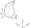
在超颖光学器件100、101、102、103、104和105中采用的第一纳米结构NS1、第二纳米结构NS2和第三纳米结构NS3可以具有如图15A所示的方柱形状或如图15B所示的圆柱形状。此处,高度H可以对应于h1、h2或h3,并且宽度D可以对应于w1、w2或w3。可以使用如图15C所示的截四角锥形状或如图15D所示的截圆锥形状。The first nanostructure NS1 , the second nanostructure NS2 and the third nanostructure NS3 employed in the meta-
另外,矩形形状、十字形、多边形形状、椭圆形状、圆环形状或多边环形形状可以用作截面的形状。当采用环形形状作为截面的形状时,可以将不同的材料应用于截面的内部和环形部分。In addition, a rectangular shape, a cross shape, a polygonal shape, an oval shape, a circular ring shape, or a polygonal ring shape can be used as the shape of the cross section. When an annular shape is employed as the shape of the cross-section, different materials can be applied to the inner and annular portions of the cross-section.
不仅上述一般形状,而且具有局部子特征的形状也可以应用于第一纳米结构NS1、第二纳米结构NS2和第三纳米结构NS3。例如,可以将特定尺寸的凹形或凸形形状的特征添加到图15A至图15D所示的形状。Not only the general shapes described above, but also shapes with local sub-features can be applied to the first nanostructure NS1 , the second nanostructure NS2 and the third nanostructure NS3 . For example, concave or convex shaped features of a specific size can be added to the shapes shown in Figures 15A-15D.
通过根据所期望的波段中的光学性能设置目标相位曲线,上述超颖光学器件可以表现出各种光学功能。另外,因为相位不连续性可以被最小化,所以可以提高指示上述光学功能的光学效率。因为可以将根据波长的相位延迟色散
上述超颖光学器件适用于各种类型的电子设备。例如,这种超颖光学器件可以安装在诸如智能电话、可穿戴设备、物联网(IoT)设备、家用电器、平板个人计算机(PC)、个人数字助理(PDA)、便携式多媒体播放器(PMP)、导航设备、无人机、机器人、无人驾驶汽车、自动驾驶车辆和高级驾驶员辅助系统(ADAS)之类的电子设备中。The above-mentioned meta-optics are suitable for use in various types of electronic devices. For example, such meta-optics can be installed in devices such as smartphones, wearables, Internet of Things (IoT) devices, home appliances, tablet personal computers (PCs), personal digital assistants (PDAs), portable multimedia players (PMPs) , navigation devices, drones, robots, driverless cars, autonomous vehicles, and electronic devices such as advanced driver assistance systems (ADAS).
图16是根据实施例的电子设备的示意性框图。16 is a schematic block diagram of an electronic device according to an embodiment.
参考图16,在网络环境2200中,电子设备2201可以通过第一网络2298(例如,短距离无线通信网络等)与另一电子设备2202通信,或者通过第二网络2299(例如,长距离无线通信网络等)与另一电子设备2204和/或服务器2208通信。电子设备2201可以通过服务器2208与电子设备2204通信。电子设备2201可以包括处理器2220、存储器2230、输入设备2250、声音输出设备2255、显示设备2260、音频模块2270、传感器模块2210、接口2277、触觉模块2279、相机模块2280、电源管理模块2288、电池2289、通信模块2290、订户识别模块2296和/或天线模块2297。在电子设备2201中,可以省略这些组件中的一些组件(例如,显示设备2260),或者可以添加其他组件。这些组件中的一些组件可以一起实现为一个集成电路。例如,传感器模块2210的指纹传感器2211、虹膜传感器、照度传感器等可以被嵌入在显示设备2260(例如,显示器等)中。16, in a
处理器2220可以执行软件(例如,程序2240)以控制与其连接的电子设备2201之一或多个其他组件(例如,硬件、软件组件等),并执行各种数据处理或操作。作为数据处理或操作的一部分,处理器2220可以将从其他组件(例如,传感器模块2210、通信模块2290等)接收到的命令和/或数据加载到易失性存储器2232,处理易失性存储器2232中存储的命令和/或数据,并且将结果数据存储在非易失性存储器2234中。处理器2220可以包括主处理器2221(例如,中央处理单元、应用处理器等)、以及可独立于主处理器2221操作或可与主处理器2221一起操作的辅助处理器2223(例如,图形处理设备、图像信号处理器、传感器集线器处理器、通信处理器等)。辅助处理器2223可以比主处理器2221使用更少的电力,并且执行专门的功能。
辅助处理器2223可以在主处理器2221处于非活动状态(例如,睡眠状态)时代替主处理器2221,或在主处理器2221处于活动状态(例如,应用执行状态)时与主处理器2221一起,控制与电子设备2201的一些组件(例如,显示设备2260、传感器模块2210、通信模块2290等)有关的功能和/或组件的状态。辅助处理器2223(例如,图像信号处理器、通信处理器等)可以被实现为在功能上与辅助处理器2223相关的另一组件(例如,相机模块2280、通信模块2290等)的一部分。The
存储器2230可以存储电子设备2201的组件(例如,处理器2220、传感器模块2210等)所必需的各种类型的数据。该数据可以包括例如软件(例如,程序2240等)以及有关与其相关联的命令的输入数据和/或输出数据。存储器2230可以包括易失性存储器2232和/或非易失性存储器2234。The
可以将程序2240作为软件存储在存储器2230中,并且程序2240包括操作系统2242、中间件2244和/或应用2246。
输入设备2250可以从电子设备2201的外部(例如,用户等)接收相对于电子设备2201的组件(例如,处理器2220等)要使用的命令和/或数据。输入设备2250可以包括麦克风、鼠标、键盘和/或数字笔(例如,触控笔等)。
声音输出设备2255可以向电子设备2201的外部输出声音信号。音频输出设备2255可以包括扬声器和/或听筒。扬声器可以用于一般目的(例如,回放多媒体或重现记录的数据),而听筒可以用于接收来电。听筒可以耦接到扬声器作为扬声器的一部分,或者可以被实现为独立于扬声器的单独设备。The
显示设备2260可以可视地向电子设备2201的外部提供信息。显示设备2260可以包括显示器、全息设备或投影仪、以及用于控制显示器、全息设备或投影仪的控制电路。显示设备2260可以包括被配置为感测触摸的触摸电路、和/或被配置为测量由触摸产生的力的强度的传感器电路(例如,压力传感器)。The
音频模块2270可以将声音转换为电信号,或者将电信号转换为声音。音频模块2270可以通过输入设备2250获得声音,或者可以通过声音输出设备2255、直接或无线地连接到电子没备2201的另一电子设备(例如,电子设备2202)的扬声器和/或耳机输出声音。The
传感器模块2210可以检测电子设备2201的操作状态(例如,功率、温度等)或外部环境状态(用户状态等),并且生成与所检测到的状态相对应的电信号和/或数据值。传感器模块2210可以包括指纹传感器2211、加速度传感器2212、位置传感器2213、3D传感器2214等,并且还可以包括虹膜传感器、陀螺仪传感器、压力传感器、磁性传感器、握持传感器、接近传感器、颜色传感器、红外(IR)传感器、生物传感器、温度传感器、湿度传感器和/或照度传感器。The
3D传感器2214可以被配置为通过向对象发射光并分析从对象反射的光来感测对象的形状或移动,并且可以包括根据上述实施例的超颖光学器件100、101、102、103、104和105之一。The
接口2277可以支持用于将电子设备2201直接或无线地连接到另一电子设备(例如,电子设备2202等)的一个或多个指定协议。接口2277可以包括高清多媒体接口(HDMI)、通用串行总线(USB)接口、安全数字(SD)卡接口和/或音频接口。
连接端子2278可以包括用于将电子设备2201物理地连接到另一电子设备(例如,电子设备2202等)的连接器。连接端子2278可以包括HDMI连接器、USB连接器、SD卡连接器和/或音频连接器(耳机连接器等)。
触觉模块2279可以将电信号转换成机械刺激(例如,振动、运动等)或电刺激,使得用户可以通过触觉或运动感觉来识别电信号。触觉模块2279可以包括电机、压电元件和/或电刺激器件。The
相机模块2280可以捕捉静态图像和运动图片。相机模块2280可以包括包含一个或多个镜头的镜头组件、图像传感器、图像信号处理器和/或闪光灯。包括在相机模块2280中的镜头组件可以收集从作为图像捕捉目标的对象发射的光,并且包括根据上述实施例的超颖光学器件100、101、102、103、104和105之一。The
电源管理模块2288可以管理向电子设备2201供应的电力。电源管理模块2288可以被实现为电源管理集成电路(PMIC)的一部分。The
电池2289可以向电子设备2201的组件供电。电池2289可以包括不可再充电的原电池、可再充电的二次电池和/或燃料电池。The
通信模块2290可以在电子设备2201和另一电子设备(例如,电子设备2202、电子设备2204、服务器2208等)之间建立直接(有线)通信信道和/或无线通信信道,并支持通过所建立的通信信道进行通信。通信模块2290可以包括一个或多个通信处理器,其独立于处理器2220(例如,应用处理器等)操作,并支持直接通信和/或无线通信。通信模块2290可以包括无线通信模块2292(例如,蜂窝通信模块、短距离无线通信模块、全球导航卫星系统(GNSS)通信模块等)和/或有线通信模块2294(例如,局域网(LAN)通信模块、电力线通信模块等)。在这些通信模块中,相应通信模块可以通过第一网络2298(例如,诸如蓝牙、Wi-Fi直连或红外数据协会(IrDA)之类的短程通信网络)或第二网络2299(例如,诸如蜂窝网络、互联网或计算机网络(例如,LAN、WAN等)的长距离通信网络)与另一电子设备进行通信。这些各种类型的通信模块可以集成到一个组件(例如,单个芯片等)中,或者实现为多个单独的组件(例如,多个芯片)。无线通信模块2292可以基于存储在订户识别模块2296中的订户信息(例如,国际移动订户标识符(IMSI)等)识别和认证通信网络(例如,第一网络2298和/或第二网络2299)中的电子设备2201。The
天线模块2297可以向外部(例如,另一电子设备等)发送信号和/或电力或从外部接收信号和/或电力。天线模块2297可以包括辐射器,该辐射器在基板(例如,印刷电路板(PCB)等)上包括导电图案。天线模块2297可以包括一个或多个天线。当天线模块2297中包括多个天线时,通信模块2290可以从多个天线中选择适合于在通信网络(例如,第一网络2298和/或第二网络2299)中采用的通信方法的天线。可以经由所选的天线在通信模块2290和另一电子设备之间发送或接收信号和/或电力。除了天线之外,其他组件(例如,射频集成电路(RFIC)等)也可以被设置为天线模块2297的一部分。The
这些组件中的一些组件可以相互连接,并通过通信方法(例如,总线、通用输入和输出(GPIO)、串行外围接口(SPI)或移动工业处理器接口(MIPI))相互交换信号(例如,命令、数据等)。Some of these components can be connected to each other and exchange signals with each other (eg, bus, general purpose input and output (GPIO), serial peripheral interface (SPI), or mobile industry processor interface (MIPI)) via communication methods (eg, commands, data, etc.).
可以通过连接到第二网络2299的服务器2208在电子设备2201和电子设备2204(其是外部设备)之间发送或接收命令或数据。其他电子设备2202和2204可以是与电子设备2201相同类型或不同类型的设备。可以由其他电子设备2202、2204或2208中的至少一个执行要由电子设备2201执行的全部或一些操作。例如,当要由电子设备2201执行功能或服务时,可以请求一个或多个其他电子设备执行该功能或服务的全部或一部分,而不是由电子设备2201执行该功能或服务。接收到请求的一个或多个其他电子设备可以执行与请求相关联的附加功能或服务,并向电子设备2201发送执行附加功能的结果。为此,可以使用云计算、分布式计算和/或客户端-服务器计算技术。Commands or data may be sent or received between the
图17是包括在图16的电子设备2201中的相机模块2280的示意性框图。FIG. 17 is a schematic block diagram of the
参考图17,相机模块2280可以包括镜头组件2310、闪光灯2320、图像传感器2330、图像稳定器2340、存储器2350(缓冲存储器等)和/或图像信号处理器2360。镜头组件2310可以收集从作为图像捕捉目标的对象发射的光,并且包括上述超颖光学器件100、101、102、103、104和105之一。镜头组件2310可以包括一个或多个折射透镜和超颖光学器件。可以将超颖光学器件设计为具有目标相位延迟曲线的透镜,该透镜相对于宽波段表现出恒定的聚光效率。包括超颖光学器件的镜头组件2310可以具有所期望的光学性能,并且可以具有短的光学长度。17 , the
相机模块2280还可以包括致动器。致动器可以驱动镜头组件2310的透镜元件移动,并调节透镜元件之间的距离,例如,以进行变焦和/或自动聚焦(AF)。The
相机模块2280可以包括多个镜头组件2310,并且在这种情况下,可以用作双相机、360度相机或球形相机。多个镜头组件2310中的一些可以具有相同的镜头属性(例如,视角、焦距、自动对焦、F数、光学变焦等)或不同的镜头属性。镜头组件2310可以包括广角镜头或远摄镜头。The
闪光灯2320可以发射光以用于增强从对象发射或反射的光。闪光灯2320可以包括一个或多个发光二极管(LED)(红绿蓝(RGB)LED)和氙气灯。图像传感器2330可以将从对象发射或反射并透射通过镜头组件2310的光转换成电信号以获得与对象相对应的图像。图像传感器2330可以包括从具有不同属性的图像传感器中选择的一个或多个传感器,例如,RGB传感器、黑白(BW)传感器、红外(IR)传感器和紫外(UV)传感器。包括在图像传感器2330中的每个传感器可以被实现为电荷耦合器件(CCD)传感器和/或互补金属氧化物半导体(CMOS)传感器。The
图像稳定器2340可以响应于相机模块2280或包括相机模块2280的电子设备2201的移动,沿特定方向移动包括在镜头组件2310中的一个或多个透镜或图像传感器2330或控制图像传感器2330的操作特性(例如,读出定时等),从而补偿由于移动产生的负面影响。图像稳定器2340可以通过使用设置在相机模块2280内部或外部的陀螺仪传感器(未示出)或加速度传感器(未示出)来检测相机模块2280或电子设备2201的移动。图像稳定器2340可以以光学方式实现。The
存储器2350可以存储通过图像传感器2330获得的一些或全部图像以用于接下来的图像处理操作。例如,当高速地获得多个图像时,所获得的源数据(例如,拜耳模式数据、高分辨率数据等)可以存储在存储器2350中,并且仅低分辨率图像可以被显示并用于向图像信号处理器2360发送所选图像(例如,由用户选择的图像等)的源数据。存储器2350可以被集成到电子设备2201的存储器2230中,或者被实现为独立操作的单独存储器。The
图像信号处理器2360可以对由图像传感器2330获得的图像或存储在存储器2350中的图像数据执行一个或多个图像处理操作。一个或多个图像处理操作可以包括:生成深度图、3D建模、生成全景图像、提取特征点、合成图像和/或图像补偿(例如,降噪、分辨率调整、亮度调整、模糊、锐化、柔化等)。图像信号处理器2360可以对相机模块2280的组件(例如,图像传感器2330等)执行控制(例如,曝光时间控制或读取定时控制等)。由图像信号处理器2360处理的图像可以被存储在存储器2350中以被附加地处理,或者可以被提供给相机模块2280的外部组件(例如,存储器2230、显示设备2260、电子设备2202、电子设备2204、服务器2208等)。图像信号处理器2360可以被集成到处理器2220中,或者可以被实现为独立于处理器2220操作的单独处理器。当图像信号处理器2360被实现为独立于处理器2220的处理器时,由图像信号处理器2360处理的图像可以附加地由处理器2220进行图像处理,并显示在显示设备2260上。
电子设备2201可以包括具有不同属性或功能的多个相机模块2280。在这种情况下,多个相机模块2280之一可以是广角相机,而另一个可以是远摄相机。类似地,多个相机模块2280之一可以是前置相机,而另一个可以是后置相机。The
图18是设置在图16的电子设备2201中的3D传感器2214的示意性框图。FIG. 18 is a schematic block diagram of the
3D传感器2214向对象发射光,并且接收并分析从对象反射的光以感测对象的形状、移动等。3D传感器2214包括光源2420、超颖光学器件2410、光电探测器2430、信号处理器2440和存储器2450。根据上述实施例的超颖光学器件100、101、102、103、104和105之一可以用作超颖光学器件2410,并且目标相位延迟曲线可以被设置为允许超颖光学器件2410作为光束偏转器或光束整形器。The
光源2420发射光以用于分析对象的形状和位置。光源2420可以包括用于产生并发射特定波长的光的光源。光源2420可以包括诸如激光二极管(LD)、LED或超发光二极管之类的光源,该光源产生并发射适合于分析对象的位置和形状的波段的光。光源2420可以是波长可变的激光二极管。光源2420可以产生并发射多个不同波段的光。光源2420可以产生并发射脉冲光或连续光。The
超颖光学器件2410对从光源2420发射的光进行调制,并向对象发射调制后的光。当超颖光学器件2410是光束偏转器时,超颖光学器件2410可以使入射光在特定方向上朝对象偏转。当超颖光学器件2410是光束整形器时,超颖光学器件2410对入射光进行调制,使得入射光具有特定图案的分布。超颖光学器件2410可以形成适合于3D形状分析的结构化光。The meta-
如上所述,超颖光学器件2410可以相对于宽带的波长表现出恒定的衍射效率。因此,可以以提高的精度或以相对于波长没有偏差的所期望的光束图案来执行光束转向。As described above, meta-
光电探测器2430接收穿过超颖光学器件2410并发射到对象的光的反射光。光电探测器2430可以包括用于感测光的多个传感器的阵列,或者可以仅包括一个传感器。The
信号处理器2440可以处理由光电探测器2430感测到的信号以分析对象的形状等。信号处理器2440可以分析包括对象的深度位置的3D形状。The
为了分析3D形状,可以执行用于测量光的飞行时间的操作。各种操作方法可以用于测量光的飞行时间。例如,在直接时间测量方法中,通过向对象发射脉冲光并测量接收从对象反射并返回的光所花费的时间来测量到对象的距离。在相关方法中,向对象发射脉冲光,并基于从对象反射并返回的光的亮度,测量到对象的距离。在相位延迟测量方法中,向对象发射诸如正弦波之类的连续波的光,并且检测该光与从对象反射并返回的反射光之间的相位差并将其转换为距离。In order to analyze the 3D shape, an operation for measuring the time of flight of light can be performed. Various manipulation methods can be used to measure the time of flight of light. For example, in a direct time measurement method, the distance to an object is measured by emitting pulsed light at the object and measuring the time it takes to receive the light reflected from the object and back. In a related method, pulsed light is emitted at an object, and the distance to the object is measured based on the brightness of the light reflected from the object and back. In the phase delay measurement method, light of a continuous wave such as a sine wave is emitted to an object, and a phase difference between the light and the reflected light reflected from and returned from the object is detected and converted into a distance.
当结构化光被发射到对象时,可以根据从对象反射的结构化光的图案的变化(即,根据将结构化光的图案与反射的结构化光的图案进行比较的结果)来计算对象的深度位置。可以通过在各种坐标下跟踪从对象反射的反射结构化光的图案的变化来提取对象的深度信息,并且可以从该深度信息中提取与对象的形状和移动有关的3D信息。When structured light is emitted to an object, the object's light can be calculated from changes in the pattern of structured light reflected from the object (ie, from the result of comparing the pattern of structured light with the pattern of reflected structured light). depth position. Depth information of an object can be extracted by tracking changes in the pattern of reflected structured light reflected from the object at various coordinates, and 3D information related to the shape and movement of the object can be extracted from the depth information.
存储器2450可以存储用于信号处理器2440的操作的程序和其他数据。The
信号处理器2440的操作结果(即,关于对象的形状和位置的信息)可以被发送到包括在电子设备2201中的另一单元或另一电子设备。例如,该信息可以由存储在存储器2230中的应用2246使用。操作结果被发送到的另一电子设备可以是输出结果的显示设备或打印机。备选地,其他电子设备可以是但不限于自动驾驶设备(例如,无人驾驶汽车、自动驾驶车辆、机器人或无人机)、智能电话、智能手表、蜂窝电话、PDA、膝上型PC、各种类型的可穿戴设备、其他移动或非移动计算设备或IoT设备。The operation result of the signal processor 2440 (ie, information on the shape and position of the object) may be transmitted to another unit included in the
上面已经参考附图中示出的实施例描述了超颖光学器件和包括超颖光学器件的电子设备,但是它们仅是示例,并且对于本领域的普通技术人员显然的是,可以进行各种修改,并且其他等效实施例是可推导出的。因此,本文阐述的实施例应当被认为仅是描述性的,而不是为了限制的目的。本公开的范围在权利要求中而不是在前面的描述中进行阐述,并且落入与其等效的范围内的所有差异应被解释为包括在本公开中。The meta-optics and the electronic device including the meta-optics have been described above with reference to the embodiments shown in the accompanying drawings, but they are only examples, and it will be apparent to those of ordinary skill in the art that various modifications can be made , and other equivalent embodiments are derivable. Accordingly, the embodiments set forth herein should be regarded as illustrative only and not for purposes of limitation. The scope of the present disclosure is set forth in the appended claims, rather than the foregoing description, and all differences that come within the equivalency thereof should be construed as being included in the present disclosure.
超颖光学器件使用布置在多层(即,三层或更多层)中的纳米结构,并且可以调节每一层的折射率的变化和色散的变化,以相对于期望波段的光实现所期望的相位延迟曲线。Metaoptics use nanostructures arranged in multiple layers (i.e., three or more layers) and can tune the changes in refractive index and dispersion of each layer to achieve the desired relative to the desired wavelength band of light phase delay curve.
超颖光学器件可以相对于宽波段的光表现出高衍射效率。Metaoptics can exhibit high diffraction efficiency with respect to broadband light.
超颖光学器件可以用作透镜、光束偏转器、光束整形器等,并且适用于使用它们的各种类型的电子设备。Metaoptics can be used as lenses, beam deflectors, beam shapers, etc., and are applicable to various types of electronic devices that use them.
应当理解的是,本文描述的实施例应当被认为仅是描述性的,而不是为了限制的目的。对每个实施例中的特征或方面的描述通常应被看作可用于其他实施例中的其他类似特征或方面。尽管已参照附图描述了一个或多个实施例,但本领域普通技术人员应当理解,在不脱离所附权利要求所限定的精神和范围的情况下,可以进行形式和细节上的多种改变。It should be understood that the embodiments described herein are to be regarded as illustrative only and not for purposes of limitation. Descriptions of features or aspects in each embodiment should generally be considered as available for other similar features or aspects in other embodiments. Although one or more embodiments have been described with reference to the accompanying drawings, workers of ordinary skill in the art will recognize that various changes in form and details may be made therein without departing from the spirit and scope as defined by the appended claims .
Claims (28)
Translated fromChineseApplications Claiming Priority (2)
| Application Number | Priority Date | Filing Date | Title |
|---|---|---|---|
| KR10-2021-0004239 | 2021-01-12 | ||
| KR1020210004239AKR102857451B1 (en) | 2021-01-12 | 2021-01-12 | Meta lens and electronic apparatus including the same |
Publications (1)
| Publication Number | Publication Date |
|---|---|
| CN114764155Atrue CN114764155A (en) | 2022-07-19 |
Family
ID=77520551
Family Applications (1)
| Application Number | Title | Priority Date | Filing Date |
|---|---|---|---|
| CN202110964676.2APendingCN114764155A (en) | 2021-01-12 | 2021-08-18 | Metastics optical device and electronic apparatus including the same |
Country Status (4)
| Country | Link |
|---|---|
| US (1) | US12066696B2 (en) |
| EP (1) | EP4027174A1 (en) |
| KR (1) | KR102857451B1 (en) |
| CN (1) | CN114764155A (en) |
Families Citing this family (6)
| Publication number | Priority date | Publication date | Assignee | Title |
|---|---|---|---|---|
| CN114217413B (en)* | 2021-12-13 | 2023-08-11 | 中国科学院光电技术研究所 | A metasurface-based ultra-wide-angle broadband polarization imaging system and detection equipment |
| JP2023150097A (en)* | 2022-03-31 | 2023-10-16 | セイコーエプソン株式会社 | Phase modulation element, projector, and head-mounted display |
| US20240322056A1 (en)* | 2023-03-21 | 2024-09-26 | Visera Technologies Company Ltd. | Optical device |
| JP2025036894A (en)* | 2023-09-05 | 2025-03-17 | ソニーセミコンダクタソリューションズ株式会社 | Photodetection device, optical element, and electronic device |
| WO2025157906A1 (en)* | 2024-01-23 | 2025-07-31 | Nil Technology Aps | Camera modules incorporating metasurfaces |
| US20250297855A1 (en)* | 2024-03-21 | 2025-09-25 | Kla Corporation | System and method for device-like overlay targets measurement |
Family Cites Families (14)
| Publication number | Priority date | Publication date | Assignee | Title |
|---|---|---|---|---|
| KR101593506B1 (en) | 2011-04-20 | 2016-02-12 | 휴렛-팩커드 디벨롭먼트 컴퍼니, 엘.피. | Sub-wavelength grating-based optical elements |
| JP5957877B2 (en) | 2011-12-26 | 2016-07-27 | 旭硝子株式会社 | Metamaterial manufacturing method and metamaterial |
| US9946051B2 (en)* | 2015-04-22 | 2018-04-17 | Samsung Electronics Co., Ltd. | Imaging apparatus and image sensor including the same |
| US20180196138A1 (en)* | 2017-01-10 | 2018-07-12 | Samsung Electronics Co., Ltd. | Optical modulating device and system including the same |
| KR102587958B1 (en)* | 2017-02-03 | 2023-10-11 | 삼성전자주식회사 | Meta optical device and method of fabricating the same |
| US10613254B2 (en) | 2017-05-24 | 2020-04-07 | Uchicago Argonne, Llc | Ultrathin, polarization-independent, achromatic metalens for focusing visible light |
| DE112018002670T5 (en) | 2017-05-24 | 2020-03-05 | The Trustees Of Columbia University In The City Of New York | Broadband achromatic flat optical components due to dispersion-technical dielectric meta-surfaces |
| KR20190033283A (en)* | 2017-09-21 | 2019-03-29 | 삼성전자주식회사 | Metasurface optical element and method of manufacturing the same |
| US10365535B2 (en) | 2017-12-18 | 2019-07-30 | Intel Corporation | Broadband flat optical elements and methods of manufacture |
| WO2020068844A1 (en) | 2018-09-25 | 2020-04-02 | President And Fellows Of Harvard College | Broadband achromatic polarization-insensitive metalens with anisotropic nanostructures |
| KR102129862B1 (en) | 2018-12-11 | 2020-07-03 | 포항공과대학교 산학협력단 | Metalens, manufacturing method thereof and optical device having the same |
| CN109683310A (en) | 2019-01-10 | 2019-04-26 | 上海理工大学 | A kind of super surface design method of cascade that THz wave ultra wide band achromatism focuses |
| CN111158070B (en) | 2020-02-25 | 2021-09-28 | 南京大学 | Double-layer achromatic lens based on all-dielectric super-surface |
| US12066592B2 (en) | 2020-02-28 | 2024-08-20 | Samsung Electronics Co., Ltd. | Meta-optical device and electronic apparatus including the same |
- 2021
- 2021-01-12KRKR1020210004239Apatent/KR102857451B1/enactiveActive
- 2021-08-12USUS17/400,840patent/US12066696B2/enactiveActive
- 2021-08-18CNCN202110964676.2Apatent/CN114764155A/enactivePending
- 2021-08-27EPEP21193459.1Apatent/EP4027174A1/enactivePending
Also Published As
| Publication number | Publication date |
|---|---|
| KR20220102040A (en) | 2022-07-19 |
| US20220221741A1 (en) | 2022-07-14 |
| US12066696B2 (en) | 2024-08-20 |
| KR102857451B1 (en) | 2025-09-08 |
| EP4027174A1 (en) | 2022-07-13 |
Similar Documents
| Publication | Publication Date | Title |
|---|---|---|
| JP7690298B2 (en) | Meta-optical element and electronic device including same | |
| CN114764155A (en) | Metastics optical device and electronic apparatus including the same | |
| US12066740B2 (en) | Meta-optical device having variable performance and electronic device including the same | |
| US12174367B2 (en) | Meta optical device and electronic apparatus including the same | |
| US20230127423A1 (en) | Lens assembly, imaging apparatus including the lens assembly, and electronic apparatus including the lens assembly | |
| KR20210110150A (en) | Meta lens and electronic apparatus including the same | |
| US12174339B2 (en) | Meta-lens, imaging optics, and electronic device including the same | |
| US12032266B2 (en) | Phase modulator and phase modulator array including the same | |
| CN115621290A (en) | Optical sensor and electronic device including the same | |
| KR20230060436A (en) | Lens assembly, imaging apparatus and electronic apparatus employing the same | |
| KR20230020336A (en) | Meta-lens, imaging optics, electronic device including the same | |
| KR20230065770A (en) | Meta-optical device and method of manufacturing the same | |
| US11822106B2 (en) | Meta optical device and electronic apparatus including the same | |
| CN115704933A (en) | Meta-optics device and electronic device including meta-optics device | |
| CN114430467A (en) | Image sensor including dichroic lens array and electronic device including the same | |
| EP4215955B1 (en) | Meta-optical device and electronic device including the same | |
| KR102843332B1 (en) | Meta optical device and electronic apparatus including the same | |
| EP4067946B1 (en) | Display device and electronic device including the same | |
| KR102871503B1 (en) | Meta optical device with variable performance and electronic apparatus including the same | |
| KR20230042979A (en) | Metaoptics and method of manufacturing metasurface | |
| KR20220086457A (en) | Meta optical device with variable performance and electronic apparatus including the same | |
| KR20220137512A (en) | Display apparatus and electronic apparatus including the same |
Legal Events
| Date | Code | Title | Description |
|---|---|---|---|
| PB01 | Publication | ||
| PB01 | Publication | ||
| SE01 | Entry into force of request for substantive examination | ||
| SE01 | Entry into force of request for substantive examination |